Embed Size (px)
Citation preview
8/13/2019 Video Amplifier Design Based on Op Amps
http://slidepdf.com/reader/full/video-amplifier-design-based-on-op-amps 1/3
LETTERS O THE’EDITOR 169
ments we have performed have shown the true practicality ofthis single parameter control of w,,. It should be mentioned thatthere are some other biquadratic structures [16], [17] whichalso have the ability of varying f0 and Q independently withresistors, but they require three or more amplifiers and theposition of the resistors is inconvenient.
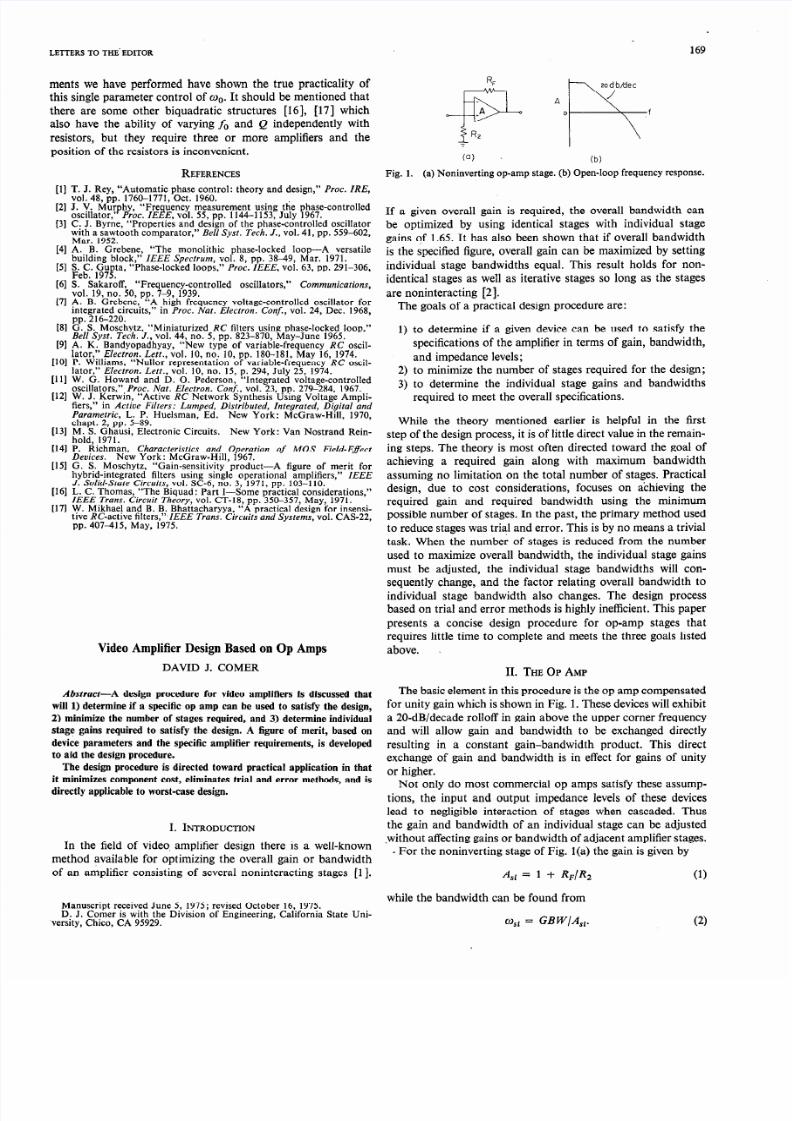
RF rodb/dec
A/
- +A
a I+
0 1
R2
(a) (b)REFERENCES Fig. 1. (a) Noninverting op-amp stage. (b) Open-loop frequen cy response.
[l] T. J. Rey, “Automatic phase control: theory and design,” Proc. IRE,vol. 48, pp. 1760-1771, Oct. 1960.[2] J. V. Murphy, “Frequency measurement using the phase-controlled
oscillator,” Proc. IEEE, vol. 55, pp. 1144-l 153, July 1967. If a given overall gain is required, the overall bandwidth can[3] C. J. Byrne, “Properties and design of the phase-controlled oscillator
with a sawtooth comparator,” Bell Syst. Tech. J., vol. 41, pp. 559-602,be optimized by using identical stages with individual stage
Mar. 1952. gains of 1.65. It has also been shown that if overall bandwidth141 A. B. Grebene, “The monolithic phase-locked loop--A versatile
building bloc&” IEEE @e&urn, vol. 8, pp. 3849, Mar. 1971.is the specified figure, overall gain can be maximized by setting
[5] Eeg. lCii ta, Phase-loc ked loops, ” Proc. IEEE, vol. 63, pp. 291-306, individual stage bandwidths equal. This result holds for non-
[6] S. Sakaroff, “Frequency-controlled oscillators,” Communications,identical stages as well as iterative stages so long as the stages
vol. 19, no. 50, pp. 7-9, 1939 .[7] A. B. Grebene,, “A high frequency voltage-controlled oscillator for
are noninteracting 121.
integrated c ircuns,” in Proc. Nar. Electron. Conf., vol. 24, Dec. 1968, The goals of a practical design procedure are:pp. 216-220.
[8] G. S. Moschytz, “Miniaturized RC filters using phase-locked loop,”Bell Syst. Tech. J., vol. 44, no. 5, pp. 823-870, May-June 1965.
[9] A. K. Bandyopadhyay, “New type of variable-frequency RC oscil-lator,” Electron. Lett., vol. 10, no. 10, pp. 180-181, May 16, 1974.
[lo] P. Williams, “Nullor representation of variable-frequency RC oscil-later,” Electron. L ett., vol. 10, no. 15, p. 294, July 25, 1974.
[ll] W. G. Howard and D. 0. Pederson, “Integrated voltage-controlled
1) to determine if a given device can be used to satisfy thespecifications of the amplifier in terms of gain, bandwidth,and impedance levels;
2) to minimize the number of stages required for the design;
oscillators ,” Proc. Nat. Electron. Conf., vol. 23, pp. 219-284, 1967. 3) to determine the individual stage gains and bandwidths[12] W. J. Kerwin, “Active RC Network Synthesis Using Voltage Ampli-
fiers,” in Active Filters: Lump ed, Distributed, Integrated, Digital andrequired to meet the overall specifications.
Parametric, L. P. Huelsman, Ed. New York: McGraw-Hill, 1970,chapt. 2, pp. 5-89. While the theory mentioned earlier is helpful in the first
[13] M. S. Ghausi, Electronic Circuits. New York: Van Nostrand Rein-hold, 1971.
step of the design process, t is of little direct value in the remain-[14] P. Richman, Characteristics and Operation of MOS Field-Effect ing steps. The theory is most often directed toward the goal of
Deoices. New York: McGraw-Hill, 1967.[15] G. S. Moschytz, “Gain-sensitivity product-A figure of merit for achieving a required gain along with maximum bandwidth
hybrid-integrated filters using single operational a mplifiers ,” IEEEJ. Solid-State Circuits, v ol. SC-6, no. 3, 1971, pp. 103-11 0.
assuming no limitation on the total number of stages. Practical
[16] L. C. Thomas, “The Biquad: Part I-Some practical considerations,” design, due to cost considerations, focuses on achieving theIEEE Trans. Circuit Theory, vol. CT-18, pp. 35O357, May, 1971.
[17] W. M ikhael and B. B. Bhattacharyya? “A practical design for insensi-required gain and required bandwidth using the minimum
tive RC-active filters,” IEEE Trans. Cvcuits and Systems, vol. CAS-22, possible number of stages. n the past, the primary method usedpp. 407415, May, 1975. to reduce stageswas trial and error. This is by no means a trivial
task. When the number of stages is reduced from the numberused to maximize overall bandwidth, the individual stage gains
must be adjusted, the individual stage bandwidths will con-sequently change, and the factor relating overall bandw idth toindividual stage bandwidth also changes. The design processbased on trial and error methods is highly inefficient. This paperpresents a concise design procedure for op-amp stages thatrequires little time to comp lete and meets the three goals listed
Video Amplifier Design Based on Op Amps above.
DAVID J. COMER
Abstract-A design procedure for video amplifiers is discussed thatwill 1) determine if a specific op amp can be used to satisfy the design,2) minimize the number of stages required, and 3) determine individualstage gains required to satisfy the design. A figure of me rit, based ondevice parameters and the specific amplifier requirements, is dev elopedto aid the design procedure.
The design procedure is directed toward practical application in thatit minimizes component cost, eliminates trial and error methods, and isdirectly applicable to worst-case design.
II. THE OP AMP
The basic element in this procedure is the op amp compensatedfor unity gain which is shown in Fig. 1. These devices will exhibita 20-dB/decade rolloff in gain above the upper corner frequencyand will allow gain and bandwidth to be exchanged directlyresulting in a constant gain-bandwidth product. This direct
exchange of gain and bandwidth is in effect for gains of unityor higher.Not only do most commercial op amps satisfy these assump-
tions, the input and output impedance levels of these deviceslead to negligible interaction of stages when cascaded. Thus
I. INTR~DLJCTI~N the gain and bandwidth of an individual stage can be adjusted
In the field of video, amplifier design there is a well-known>without affecting gains or bandwidth of adjacent amplifier stages.
_method available for optimizing the overall gain or bandwidthof an amplifier consisting of several noninteracting stages [l].
For the noninverting stage of Fig. l(a) the gain is given by
A,, = 1 + RJR, (1)
while the bandwidth can be found fromManus cript received June 5, 1975; revised October 16, 1975.D. J. Comer is with the Division of Engineering, California State Uni-
versity, Chico, CA 95929. wsi = GBWIA,,. (2)
8/13/2019 Video Amplifier Design Based on Op Amps
http://slidepdf.com/reader/full/video-amplifier-design-based-on-op-amps 2/3
170 IEEETRANSACT IONS; N CIRCUITSAND SYSTEMS,M ARCH
III. MINIMIZINGTHE NUMBER F STAGES
A design procedure has been developed to minimize thenumber of transistor stages in a video amplifier [3], [4]. Thefollowing discussion indicates the modifications necessary inapplying this theory to the op amp.
The first step in the procedure consists of determining theminimum allowable gain-bandwidth product for the device to
be used. If w,, is the Tequired overall bandwidth and A,, is therequired overall voltage gain, ii can be shown [3] that the devicegain-bandwidth must equal or exceed the minimum value
GBW,,, = 2.8q,,Jh A,,. (3)
If the device gain-bandwidth is smaller than this value, theamplifier specifications cannot be,met iegkdless of the numberof stages used. If the device gain-bandwidth happens to equalthe minimum value, the amplifier can be realized using anindividual stage gain of 1.65 and n stages, where
ln A,,n = - = 2 In A,,.
In 1.65(4)
From a practical standpoint the m&t interesting case occurswhen the device gain-bandwidth exceeds the minimum value.In this instance, the amplifier could be conskucted to equal orexceed both the overall gain and bandwidth requirements.Rather than allow excess gain or bandwidth, however, it iseconomically advantageous to reduce the number of stages tothe minimum ntimber.required to achieve the overall specifica-tions. In many cases, his results in a significant reduction in thenumber of stages and component cost of the amplifier.
To calculate this minimum numb& of stages, t is first assumedthat an individdal stage gain of 1.65 is used. Since an excessoverall bandwidth results from this situation, stages can be
removed if the proper adjustment is made in individual stagegain and bandw idths. The adjusted single stage gain must be
A,, = (1.65)“‘“’ = (A,$‘“’ (5)
where m is the minimum number of stages. The adjusted singlestage bandwidth must be
q, = 1.2&o,,. (6)
The third equation necessary to find As*, Wsi, and m is given by
GB W = A,,w,,. ( 7)
The results of simultaneous solution show that the requiredvalue of A,; must satisfy
In Asi = ZAslz (8)
where
z = 1.~or2 ln 4,
GBW’ *(9)
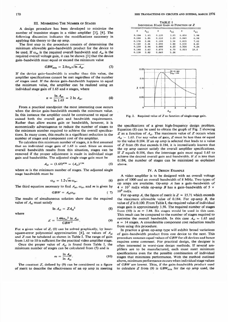
For a given value of Z, (8) can be solved graphically, by least-square-error polynomial approximation [4], or values of A,,and Z cari be tabulated as shown in Table I. The range of gainfrom 1.65 to 10 s sufficient for the practical video amplifier stage.
Once the proper value of A,, is found from Table I, theminimum number of stages can be calculated from (5) and is
In Am=L.
ln 4,
(10)
TABLE IINDIVIDUAL STAGEGAIN AS FUNCTIONOF Z
7. ‘Asi z *si 7. *si
0.184 1.65 0.120 3.05 0.050 5.98
0.180 1.85 0.110 3.29 il.040 6.98
0.170 2.06 0.100 3.56 0.035 i.62
0.160 2.26 0.090 3.88 0.030 8.42
0.150 2.44 0.080 4.25 0.b2.5 9.24
0.140 2.62 0.070 4.70 0.023 10.0
0.130 2.82 0.060 5.26
Asi
Fig. 2. Required alueof Z as unctionof single-stageain.
the specifications of a given high-frequency design probleEquation (8) can be used to obtain the graph of Fig. 2 showZ as a function of Asi. The maximum value of Z occurs whAsi = 1.65. For any value of gain, Z must be less than or eqto the value 0.184. If an op amp is selected that leads to a vaof Z frdm (9) that exceeds 0.184, it is immediately known tthe op amp cannot satisfy the overall amplifier specificatioIf Z equals 0.184, then the interstage gain must equal 1.65
achieve the desired overall gain and bandwidth. If Z is less th0.184, the number of stages can be minimized as explainabove.
IV. A DESIGN EXAMPLE
A video amplifier is to be designed with an overail voltagain of 1000 and an overall bandwidtli of 8 MHz. Two typesop amps are available. Op-amp A has a Fain-bandwidth 4 x IO’ rad/s while op-amp B has a gain-bandwidth of 510s rad/s.
For op-amp A, the figure of merit is Z = 15.71 which excethe niaximum allowable vaiue of 0.184. For op-amp B,
value of Z is 0.100. From Table I, the required value bf individu
stage gain is approximately 3.56. The required number of stafrom (10) is m = 5.44. Six stages would be used in this caThis result can be compared to the number of stages requiredoptimize’the overall bandwidth. In this case AsI = 1.65 an = 14 stages. A considerable combonent cost reduction resufrom using this procedure.
In practice a given op-ainp type will exhibit broad variatioof gain-bandwidth prdduct from one device to the next. Tprocedure assumesequal values of GB W for all devices and henrequires some comment. Fdr practical design, the designeroften interested in worst-dase design ‘methods. If several aplifiers are to be manufactured, each must meet minimuspecifications even for the possible combination of individustages that minimizes performance. With the method outlinabove, minimum performance occurs when individual stage valu
8/13/2019 Video Amplifier Design Based on Op Amps
http://slidepdf.com/reader/full/video-amplifier-design-based-on-op-amps 3/3
LETTERS O THE EDITOR 171
resulting amplifier is the worst-case design. Situations whereinworst-case design is not desired require m easurement of op-ampgain-bandwidth product to select stages of nearly identicalGB W values.
V. CONCLUSIONS“1 r
The figure of merit Z is a useful quantity in determiningwhether or not a particular op amp can be used in an amplifier
design. Rather than use trial and error techniques, the minimumnumber of stagescan be readily found from (9), (lo), and Table I.This procedure often leads to considerable reduction of com-ponent cost in the practical case.
111
PI
[31
[41
REFERENCES
M. S. Ghausi, Principles and Design of Linear Active Circuits. NewYork: McGraw-Hill, 1965.D. J. Comer and J. M. Griffith, “Optimization of bandwidth in non-iterative amplifiers,” Proc. IEEE, vol. 116, p. 384, Mar. 1969.-, “Calculating the minimu m number of iterative stages in a wide-band amplifier,” IEEE Trans. Circuit Th eory (Corresp.), vol. CT-15,pp. 280-281, Sept. 1968.-, “DesIgnable video amplifiers using base-compensated stages,”IEEE Trans. Circuit Theory, vol. (X-17, pp. 94-99, Feb. 1970.
Some New Operational-Amplifier Circuits for the
Realization of the Lossless Floating Inductance
M. A. REDDY
The usefulness of the complementary property of input andground, in linear networks containing infinite-gain differentialamplifiers, has been llustrated by Hilberman [l 1, who has shownhow, from a knowledge of this property, active-RC notch andall-pass filters can be obtained from appropriately designedbandpass filters by the very simple expedient of interchangingthe input and ground terminals. The purpose of this letter is to
give further proof of the usefulness of this complementaryproperty, by applying it to generalize existing two-operational-amplifier four-terminal gyrator circuits for lossless grounded-inductance realization, such that they can simulate also thelossless loating inductance. ’
Consider the reported two-operational-amplifier four-terminalgyrator circuits [2]-151. Attention will be restricted here to thespecial case in which all four resistors used in the circuits areequal. With the ungrounded part terminated by a capacitor, eachof these circuits can be viewed as an ideal voltage-controlledvoltage source, with a voltage gain of (1 - I/SCR) betweenthe groundei port, where the lossless grounded inductance isrealized as the driving-point impedance, and the output of oneof the operational amplifiers. A resistor is present between this
output and the driving input terminal, and by means of thisresistive feedback the desired inductance at the input is obtained.
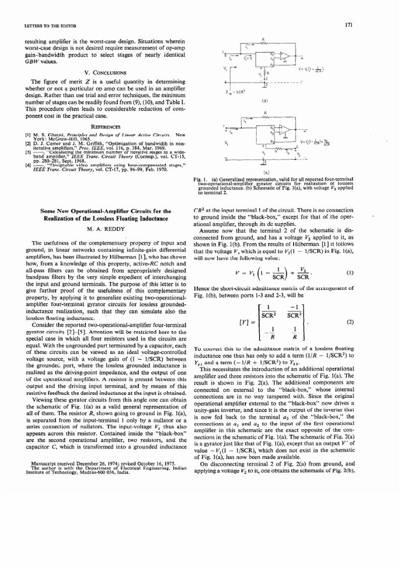
Viewing these gyrator circuits from this angle one can obtainthe schematic of Fig. l(a) as a valid general representation ofall of them. The resistor R, shown going to ground in Fig. I(a),is separated from the input-terminal 1 only by a nullator or aseries connection of nullators. The input-voltage V, thus alsoappears across this resistor. Contained inside the “black-box”are the second operational amplifier, two resistors, and thecapacitor C, which is transformed into a grounded inductance
Fig. 1. (a) Generalized representation, valid for all reported four-termina ltwo-operational-amplifier gyrator circuits for realization of losslessgrounded inductan ce. ( b) Schematic of Fig. l(a), with voltage Vz applied
to terminal 2.
CR2 at the input terminal 1 of the circuit. There is no connectionto ground inside the “black-box,” except for that of .the oper-ational amplifier, through its dc supplies.
Assume now that the terminal 2 of the schematic is dis-connected from ground, and has a voltage V, applied to it, asshown in Fig. l(b). F rom the results of Hilberman [l] it followsthat the voltage Y, which is equal to V,(l - l/SCR) in Fig. l(a),will now have the following value:
v=v,(d)+&
Hence the short-circuit admittance matrix of the arrangement ofFig. l(b), between ports l-3 and 2-3, will be
WI =
-1
SCR’
-I
1 *
i
(2)
To convert this to the admittance matrix of a lossless floatinginductance one thus has only to add a term (l/R - l/SCR’) toY,, and a term (-l/R + l/SCR’) to Y,,.
This necessitates he introduction of an additional operationalamplifier and three resistors into the schematic of Fig. l(a). Theresult is shown in Fig. 2(a). The additional components areconnected on external to the “black-box,” whose internalconnections are in no way tampered with. Since the originaloperational amplifier external to the “black-box” now drives aunity-gain inverter, and since it is the output of the inverter thatis now fed back to the terminal a3 of the “black-box,” theconnections at a1 and a2 to the input of the first operationalamplifier in this schematic are the exact opposite of the con-nections in the schematic of Fig. l(a). The schematic of Fig. 2(a)is a gyrator just like that of Fig. 1 a), except that an output V’ ofvalue - V,(l - l/SCR), which does not exist in the schematicof Fig. l(a), has now been made available.
Manuscript received December 26, 1974; revised October 16,. 1975.The author is with the Department of Electrical Engineerm g, Indian
On disconnecting terminal 2 of Fig. 2(a) from ground, and
Institute of Technology, Madras-600 036, India. applying a voltage V, to it, one obtains the schematic of Fig. 2(b),


![[PPT]Op-Amps - Georgia Institute of Technologyume.gatech.edu/mechatronics_course/OpAmp_F10.pptx · Web viewWhat is an Op-Amp? An Operational Amplifier (known as an “Op-Amp”) is](https://img.dokumen.tips/doc/110x75/5b300b187f8b9af0648e3ea2/pptop-amps-georgia-institute-of-web-viewwhat-is-an-op-amp-an-operational.jpg)