Embed Size (px)
Citation preview

Design Guide & Applications ManualFor VI-200 and VI-J00 Family DC-DC Convertersand Configurable Power Supplies
Design Guide & Applications ManualFor VI-200 and VI-J00 Family DC-DC Converters and Configurable Power Supplies
vicorpower.com 800-735-6200 Applications Engineering 1-800-927-9474 Rev. 3.0
Page 1 of 97
VI-/MI-200 and VI-/MI-J00 DC-DC Converters Section Page(s)
Zero-Current-Switching 1 2
DC-DC Converter Pinouts 2 3
Module Do’s and Don’ts 3 4 – 6
Overcurrent Protection 4 7
Output Voltage Trimming 5 8 – 10
Multiple GATE IN Connections 6 11
Application Circuits / Converter Array Design Considerations 7 12 – 13
Using Boosters and Parallel Arrays 8 14 – 17
EMC Considerations 9 18 – 28
Optional Output Filters 10 29
Battery Charger (BatMod) 11 30 – 32
Filter & Front-End Modules
AC Input Module (AIM / MI-AIM) 12 33 – 36
Harmonic Attenuator Module (HAM) 13 37 – 42
Input Attenuator Module (IAM / MI-IAM) 14 43 – 46
Ripple Attenuator Module (RAM / MI-RAM) 15 47
Offline Front End 16 48 – 51
Configurable Products
DC Input Power System (ComPAC / MI-ComPAC Family) 17 52 – 54
AC Input Power System (FlatPAC Family) 18 55 – 57
AC Input Power System (PFC FlatPAC) 19 58 – 59
General
Thermal and Module Mounting Considerations 20 60 – 67
Thermal Curves 21 68 – 77
Lead Free Pins (RoHS) 22 78 – 82
Tin Lead Pins 23 83 – 87
Module Packaging Options (SlimMod, FinMod, BusMod and MegaMod Families) 24 88
Product Weights 25 89
Glossary of Technical Terms 26 90 – 97
NOTE: This Design Guide and Applications Manual does NOT address Vicor’s Maxi, Mini and Micro DC-DCconverters. For more information on these products go to vicorpower.com .
Table of Contents

Design Guide & Applications ManualFor VI-200 and VI-J00 Family DC-DC Converters and Configurable Power Supplies
vicorpower.com 800-735-6200 Applications Engineering 1-800-927-9474 Rev. 3.0
Page 2 of 97
OVERVIEW
Vicor offers RoHS compliant modules. These modules havea “VE” prefix. The information presented herein applies toboth versions, and “VI” will be the default designation.
The heart of Vicor’s VI-/MI-200 and VI-/MI-J00 moduletechnology, zero-current-switching, allows Vicorconverters to operate at frequencies in excess of 1 MHz,with high efficiency and power density. Depending oninput voltage and load, the converters operate atfrequencies ranging from the low hundreds of kilohertz(light load, high line) to approximately one megahertz (fullload, low line). Another aspect of the Vicor topology isthat two or more power trains driven at the samefrequency will inherently load-share if their outputs aretied together. Load sharing is dynamic and is within 5%.The VI-200 and MI-200 product line offer both Driver andBooster modules:
• Drivers and Boosters must have identical power trains.
• Drivers close the voltage loop internally, Boosters do not.
• Boosters may be slaved to a Driver, allowing configurations of multi-kilowatt arrays, which exhibit dynamic current sharing between modules.
• Only a single control connection is needed between modules with all module’s power inputs and outputs, connected together — no trimming, adjustments, or external components are required to achieve load sharing.
LOSSLESS ENERGY TRANSFER
Referring to Figure and Table 1–1 below, turn-on of theMOSFET switch transfers a quantized energy packet fromthe input source to an LC “tank” circuit, composed ofinherent transformer leakage inductance of T1 and acapacitive element, C, in the secondary. Simultaneously,an approximately half-sinusoidal current flows through theswitch, resulting in switch turn-on at zero current andturn-off when current returns to zero. Resonance, orbidirectional energy flow, cannot occur because D1 willonly permit unidirectional energy transfer. A low-pass filter(Lo, Co) following the capacitor produces a low ripple DCoutput. The result is a virtually lossless energy transferfrom input to output with greatly reduced levels ofconducted and radiated noise.
Ip: Primary current
Vp: Primary voltage
Vs: Secondary voltage
OVP: Overvoltage protection (output)
OTS: Over temperature shutdown
OC1, OC2: Opto-coupler
E/A: Error amplifier
REF: Bandgap reference
C/L: Current limit amplifier
Referenced to –Vin
[a] Not in VI-J00 Series
GateOut
Vs
Vout
Vin
Ip
Vp
2.5 VREF.
Output FilterIntegrator
Vs
IpVp
MOSFET
Input Filter
OC2
OC1[a]
–S
TRIM
+S
E/A
+
+ –
+Vout
–Vout
Co
Lo
C D2
D1
ResetControl
GATEIN
-Vin
+Vin
LogicControl
Load
C/L
OTS[a]
OVP[a]
GATEOUT
–
T1
1. Zero-Current-Switching
Figure 1–1 — VI- /MI-200 and VI- /MI-J00 series zero-current-switching block diagram
Table 1–1

Design Guide & Applications ManualFor VI-200 and VI-J00 Family DC-DC Converters and Configurable Power Supplies
vicorpower.com 800-735-6200 Applications Engineering 1-800-927-9474 Rev. 3.0
Page 3 of 97
–IN, +IN. DC voltage inputs. See Tables 2–1 and 2–2 fornominal input voltages and ranges for the VI-/MI-200 andVI-/MI-J00 Family converter modules (data sheets containLow Line, 75% Max. Power and Transient ratings).
GATE OUT. The pulsed signal at the GATE OUT pin of aregulating Driver module is used to synchronously drivethe GATE IN pin of a companion Booster module to effectpower sharing between the Driver and the Booster. Daisy-chaining additional Boosters (connecting GATE OUT ofone unit to GATE IN of a succeeding unit) leads to avirtually unlimited power expansion capability.
GATE IN. The GATE IN pin on a Driver module may beused as a logic Enable / Disable input. When GATE IN ispulled low (<0.65 V @ 6 mA, referenced to –Vin), themodule is turned off; when GATE IN is floating (opencollector), the module is turned on. The open circuitvoltage of the GATE IN pin is less than 10 V.
–OUT, +OUT. DC output pins. See the Table 2–3 and 2–4below for output voltages and power levels of VI-/MI-200and VI-/MI-J00 Family converter modules.
Special output voltages from 1 – 95 V; consult factory.
T (TRIM). Provides fixed or variable adjustment of themodule output.
Trimming Down. Allows output voltage of the module tobe trimmed down, with a decrease in efficiency. Ripple asa percent of output voltage goes up and input rangewidens since input voltage dropout (loss of regulation)moves down.
Trimming Up. Reverses the above effects.
–S, +S (–SENSE, +SENSE). Provides for locating the pointof optimal voltage regulation external to the converter.Output OVP in VI- /MI-200 will trip if remote sensecompensates output voltage measured at output pinsabove 110% of nominal. Discrete wire used for sensemust be tightly twisted pair. Do not exceed 0.25 V drop innegative return; if the voltage drop exceeds 0.25 V in thenegative return path, the current limit setpoint will increase.Connect +SENSE to +OUT and –SENSE to –OUT at themodule if remote sensing is not desired. (Figure 7–4)
Figure 2–1 — VI- /MI-200, VI- /MI-J00
GATEIN
GATEOUT
+IN
–OUT
–S
T
+S
+OUT
GATEIN
GATEOUT
+IN
–OUT
–S
T
+S
–IN –IN
+OUT
Designator Low Nominal High0 10 V 12 V 20 VV 10 V 12/24 V 36 V1 21 V 24 V 32 VW 18 V 24 V 36 V2 21 V 36 V 56 V3 42 V 48 V 60 VN 36 V 48 V 76 V4 55 V 72 V 100 VT 66 V 110 V 160 V5 100 V 150 V 200 V6 200 V 300 V 400 V7 100 V 150/300 V 375 V
Designator Low Nominal High2 18 V 28 V 50 V5 100 V 155 V 210 V6 125 V 270 V 400 V7 100 V 165 V 310 V
2. DC-DC Converter Pinouts
VI-200, VI-J00 Input Voltage Ranges
Table 2–1 — VI-200, VI-J00 input voltage ranges
MI-200, MI-J00 Input Voltage Ranges
Table 2–2 — MI-200, MI-J00 input voltage ranges
Designator Output Designator OutputZ 2 V 2 15 VY 3.3 V N 18.5 V0 5 V 3 24 VX 5.2 V L 28 VW 5.5 V J 36 VV 5.8 V K 40 VT 6.5 V 4 48 VR 7.5 V H 52 VM 10 V F 72 V1 12 V D 85 VP 13.8 V B 95 V
VI-200, VI-J00 Standard Output Voltages
Table 2–3 — VI-200, VI-J00 output voltage designators
Output Power Level Power LevelVoltage VI-200 VI-J00 MI-200 MI-J00<5 Vdc 10 – 40 A 5 – 20 A 10 – 30 A 5 – 10 A≥5 Vdc 50 – 200 W 25 – 100 W 50 – 100 W 10 – 50 W
Table 2–4 — Output voltage vs. power level

Design Guide & Applications ManualFor VI-200 and VI-J00 Family DC-DC Converters and Configurable Power Supplies
vicorpower.com 800-735-6200 Applications Engineering 1-800-927-9474 Rev. 3.0
Page 4 of 97
ELECTRICAL CONSIDERATIONSGATE IN AND GATE OUT PINS
Logic Disable. When power is applied to the input pins,the GATE IN pin of a Driver can be pulled low with respectto the –IN thus turning off the output while power is stillapplied to the input. (Figure 7–1)
CAUTION: With offline applications –IN is not earth ground.
In Logic Disable mode, the GATE IN pin should be drivenfrom either an “open collector” or electromechanicalswitch that can sink 6 mA when on (GATE IN voltage lessthan 0.65 V). If driven from an electromechanical switchor relay, a 1 µF capacitor should be connected from GATE INto –IN to eliminate the effects of switch “bounce”. The 1 µFcapacitor may be required in all applications to provide a“soft start” if the unit is disabled and enabled quickly. TheGATE IN is not intended for repetitive on /off /on operationnot exceeding once per second.
High Power Arrays. The pulsed signal at the GATE OUTpin of a regulating Driver module is used to synchronouslydrive the GATE IN pin of a companion Booster module toeffect power sharing between the Driver and the Booster.(Figure 7–5) Daisy-chaining additional Boosters (i.e.,connecting GATE OUT to GATE IN of a succeeding unit)leads to a virtually unlimited power expansion capability.VI-/MI-200 series modules of the same family and powerlevel can be paralleled (i.e., Driver, VI-260-CU withBooster, VI-B60-CU).
In general:
• Don’t drive the GATE IN pin from an “analog” voltage source.
• Don’t leave GATE IN pins of Booster modules unterminated.
• Don’t overload GATE OUT; limit load to a single Vicor module GATE IN connection, or 1 kΩ, minimum, in parallel with 100 pF, maximum.
• Don’t skimp on traces that interconnect module –IN pins in high power arrays. GATE IN and GATE OUT are referenced to –IN; heavy, properly laid out traces willminimize parasitic impedances that could interfere with proper operation.
• Do use a decoupling capacitor across each module’s input (see Input Source Impedance that follows).
• Do use an EMI suppression capacitor from +/– input and output pins to the baseplate.
• Do use a fuse on each module’s + input to prevent fire in the event of module failure. See safety agency conditions of acceptability for the latest information on fusing. See link below:
http://www.vicorpower.com/technical_library/technical_documentation/quality_and_certification/safety_approvals/
Input Source Impedance. The converter should beconnected to an input source that exhibits low ACimpedance. A small electrolytic capacitor should bemounted close to the module’s input pins. (C3, Figure 3–1)This will restore low AC impedance, while avoiding thepotential resonance associated with “high-Q” filmcapacitors. The minimum value of the capacitor, inmicrofarads, should be C (µF) = 400 ÷ Vin minimum.Example: Vin, minimum, for a VI-260-CV is 200 V. Theminimum capacitance would be 400 ÷ 200 = 2 µF. Forapplications involving long input lines or high inductance,additional capacitance will be required.
The impedance of the source feeding the input of themodule directly affects both the stability and transientresponse of the module. In general, the source impedanceshould be lower than the input impedance of the moduleby a factor of ten, from DC to 50 kHz.
To calculate the required source impedance, use the following formula:
Z = 0.1(VLL)2 / Pin
where: Z is required input impedanceVLL is the low line input voltagePin is the input power of the module
Filters, which precede the module, should be well dampedto prevent ringing when the input voltage is applied orthe load on the output of the module is abruptly changed.
Input Transients. Don’t exceed the transient inputvoltage rating of the converter. Input Attenuator Modulesor surge suppressors in combination with appropriatefiltering, should be used in offline applications or inapplications where source transients may be induced byload changes, blown fuses, etc. For applications where theinput voltage may go below low line it is recommendedthat an undervoltage lockout circuit be used to pull GATEIN low to disable the converter module. The undervoltagelockout circuit should induce a delay of at least onesecond before restarting the converter module. Longerdelays will be required if external capacitance is added atthe output to insure the internal soft-start is re-initialized.
NOTE: Do not allow the rate of change of the inputvoltage to exceed 10 V/µs for any input voltage deviation.
The level of transient suppression required will depend onthe severity of the transients. A Zener diode, TRANSZORB™or MOV will provide suppression of transients under 100 µsand act as a voltage clipper for DC input transients. It maybe necessary to incorporate an LC filter for larger energytransients. This LC filter will integrate the transient energywhile the Zener clips the peak voltages. The Q of this filtershould be kept low to avoid potential resonance problems.See Section 14, Input Attenuator Module (IAM/MI-IAM)for additional information on transient suppression.
3. Module Do’s and Dont’s
Design Guide & Applications ManualFor VI-200 and VI-J00 Family DC-DC Converters and Configurable Power Supplies
vicorpower.com 800-735-6200 Applications Engineering 1-800-927-9474 Rev. 3.0
Page 5 of 97
Output OVP. The VI- /MI-200, with the exception of VI- /MI-J00s, has an internal overvoltage protection circuitthat monitors the voltage across the output power pins. Itis designed to latch the converter off at 115 – 135% ofrated output voltage. It is not a crowbar circuit, and if amodule is trimmed above 110% of rated output voltage,OVP may be activated. Do not backdrive the output ofthe converter module to test the OVP circuit.
CAUTION: When trimming up VI-/MI-J00 modules,additional care should be taken as an impropercomponent selection could result in module failure.Improper connection of the sense leads on VI-/MI-J00modules can also result in an excessive overvoltagecondition and module failure.
Input Reverse Voltage Protection. The module may beprotected against reverse input voltages by the addition ofa diode in series with the positive input, or a reverseshunt diode with a fuse in series with the positive input.See Section 14, the Input Attenuator Module (IAM /MI-IAM)provides input reverse voltage protection when used witha current limiting device (fuse).
THERMAL / MECHANICAL CONSIDERATIONS
Baseplate. Operating temperature of the baseplate, asmeasured at the center mounting slot on the –IN, –OUTside, can not exceed rated maximum. ThermMate orthermal compound should be used when mounting themodule baseplate to a chassis or heat sink. All sixmounting holes should be used. Number six (#6) machinescrews should be torqued to 5-7 in-lbs, and use of Belvillewashers is recommended.
The module pins are intended for PCB mounting either bywave soldering to a PCB or by insertion into one of therecommended PCB socket solutions.
CAUTION: Use of discrete wires soldered directly to the pins may cause intermittent or permanentdamage to the module; therefore, it is notrecommended as a reliable interconnection schemefor production as a final released product. SeeSection 21 for packaging options designed fordiscrete wire connections (BusMod, MegaMod).
In addition, modules that have been soldered into printedcircuit boards and have subsequently been removedshould not be reused.
THERMAL AND VOLTAGE HAZARDS
Vicor component power products are intended to be usedwithin protective enclosures. Vicor DC-DC converterswork effectively at baseplate temperatures, which couldbe harmful if contacted directly. Voltages and highcurrents (energy hazard) present at the pins and circuitryconnected to them may pose a safety hazard if contactedor if stray current paths develop. Systems with removablecircuit cards or covers which may expose the converter(s)or circuitry connected to the converters, should have properguarding to avoid hazardous conditions.
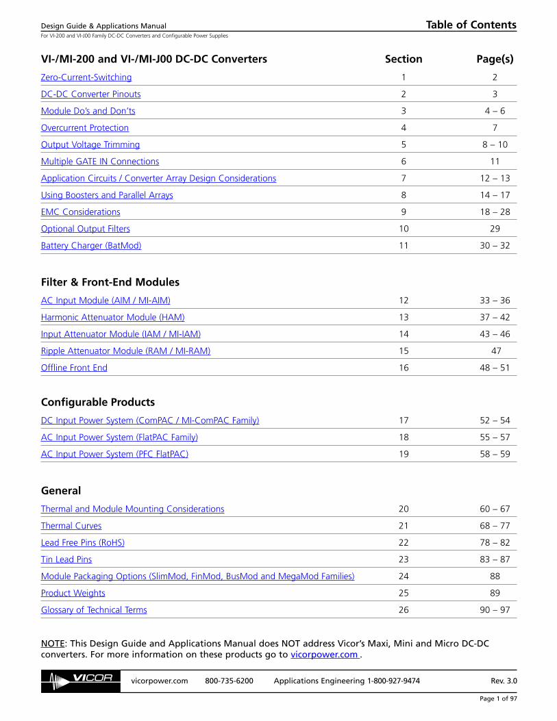
EMC CONSIDERATIONS
All applications utilizing DC-DC converters must be properlybypassed, even if no EMC standards need to be met. BypassIN and OUT pins to each module baseplate as shown inFigure 3–1. Lead length should be as short as possible.Recommended values vary depending on the front end, ifany, that is used with the modules, and are indicated on theappropriate data sheet. In most applications, C1a – C1b is a4,700 pF Y-capacitor (Vicor Part # 01000) carrying theappropriate safety agency approval; C2a – C2b is a 4,700 pFY-capacitor (Vicor Part # 01000) or a 0.01 µF ceramiccapacitor rated at 500 V. In PCB mount applications, each ofthese components is typically small enough to fit under themodule baseplate flange.
Figure 3–1 — IN and OUT pins bypassed to the module baseplateand input cap for low AC impedance
3. Module Do’s and Dont’s
+OUT+IN
–IN –OUT
Zero CurrentSwitchingConverter
C1a
C1b
C2a
C2b
C3

Design Guide & Applications ManualFor VI-200 and VI-J00 Family DC-DC Converters and Configurable Power Supplies
vicorpower.com 800-735-6200 Applications Engineering 1-800-927-9474 Rev. 3.0
Page 6 of 97
SAFETY CONSIDERATIONS
Shock Hazard. Agency compliance requires that thebaseplate be grounded.
Fusing. Internal fusing is not provided in Vicor DC-DCconverters. To meet safety agency conditions, a fuse isrequired. This fuse should be placed in the positive inputlead, not the negative input lead, as opening of thenegative input lead will cause the GATE IN and GATE OUTto rise to the potential of the +IN lead, causing possibledamage to other modules or circuits that share commonGATE IN or GATE OUT connections.
Safety agency conditions of acceptability require moduleinput fusing. The VI-x7x, VI-x6x and VI-x5x require the useof a Buss PC-Tron fuse, or other DC-rated fuse. See belowfor suggested fuse ratings.
The safety approvals section of the Vicor website shouldalways be checked for the latest fusing and conditions ofacceptability information for all DC-DC convertersincluding the MegaMod family. See link below:
http://www.vicorpower.com/technical_library/technical_documentation/quality_and_certification/safety_approvals/
Package Size Required Fuse Package Size Required Fuse
VI-27x-xx PC-Tron 2.5 A VI-J7x-xx PC-Tron 2.5 A
VI-26x-xx PC-Tron 3 A VI-J6x-xx PC-Tron 3 A
VI-25x-xx PC-Tron 5 A VI-J5x-xx PC-Tron 5 A
VI-2Tx-xx PC-Tron 5A VI-JTx-xx PC-Tron 5A
VI-24x-xx 6 A / 125 V VI-J4x-xx PC-Tron 5A
VI-2Nx-xx 8A / 125 V VI-JNx-xx PC-Tron 5A
VI-23x-xx 8 A /125 V VI-J3x-xx PC-Tron 5A
VI-22x-xx 8 A / 60 V VI-J2x-xx PC-Tron 5A
VI-2Wx-xx 12 A / 50 V VI-JWx-xx 8 A / 60 V
VI-21x-xx 12 A / 32 V VI-J1x-xx 8 A / 60 V
VI-2Vx-xx 12 A / 32 V VI-J0x-xx 8 A / 60 V
VI-20x-xx 12 A / 32 V
Acceptable Fuse Types and Current Rating for the VI-200 and VI-J00 Family of Converters
3. Module Do’s and Dont’s

Design Guide & Applications ManualFor VI-200 and VI-J00 Family DC-DC Converters and Configurable Power Supplies
vicorpower.com 800-735-6200 Applications Engineering 1-800-927-9474 Rev. 3.0
Page 7 of 97
FOLDBACK CURRENT LIMITING
The VI-/MI-200 modules with output voltages of 5 V or3.3 V incorporate foldback current limiting. (Figure 4–1) Inthis mode, the output voltage remains constant up to thecurrent knee, (Ic), which is 5 – 25% greater than full-ratedcurrent, (Imax). Beyond Ic, the output voltage falls alongthe vertical line Ic– Ifb until approximately 2 V. At ≤2 V, thevoltage and current folds back to short circuit currentpoint (20 – 80% of Imax). Typically, modules willautomatically recover when overcurrent is removed.
When bench testing modules with foldback current limiting,use a constant resistance load as opposed to a constantcurrent load. Some constant current loads have the abilityto pull full current at near zero volts. This may cause alatchup condition. Also when performing a short circuittest it is recommended to use a mercury wetted relay toinduce the output short as other methods may induceswitch bounce that could potentially damage the converter.
STRAIGHT LINE CURRENT LIMITING
The VI-/MI-200 modules with output voltages greaterthan 5 V, 2 V (VI-/MI-200 only) and all VI-/MI-J00modules incorporate a straight-line type current limit.(Figure 4–2) As output current is increased beyond Imax,the output voltage remains constant and within itsspecified limits up to a point, Ic, which is 5 – 25% greaterthan rated current, (Imax). Beyond Ic, the output voltagefalls along the vertical line to Isc. Typically, modules willautomatically recover after overcurrent is removed.
2 V
Vout
I c
I fb
Imax
IoutI short circuit
Vout
Ishort circuit
I cImax
Iout
4. Overcurrent Protection
Figure 4–1 — Foldback current limiting Figure 4–2 — Straight-line current limiting

Design Guide & Applications ManualFor VI-200 and VI-J00 Family DC-DC Converters and Configurable Power Supplies
vicorpower.com 800-735-6200 Applications Engineering 1-800-927-9474 Rev. 3.0
Page 8 of 97
OVERVIEW
Specifications such as efficiency, ripple and input voltagerange are a function of output voltage settings. As theoutput voltage is trimmed down, efficiency goes down;ripple as a percent of Vout goes up and the input voltagerange widens since input voltage dropout (loss of regulation)moves down. As the units are trimmed up, the reverse ofthe above effects occurs.
All converters have a fixed current limit. The overvoltageprotection setpoint is also fixed; trimming the outputvoltage does not alter its setting. As the output voltage istrimmed down, the current limit setpoint remains constant.Therefore, in terms of output power, if the unit is trimmeddown, available output power drops accordingly.
The output voltage of most Vicor converters can betrimmed +10%, –50%. Certain modules have restrictedtrim ranges. Consult the latest datasheet for details.
Do not attempt to trim the module output voltage morethan +10%, as overvoltage shut down may occur. Do notexceed maximum rated output power when the module istrimmed up.
CAUTION: When trimming up VI- /MI-J00 convertermodules, additional care should be taken as animproper component selection could result in modulefailure. Improper connection of the sense leads onVI- /MI-J00 converter modules can also result in anexcessive overvoltage condition and module failure.
The following procedures describe methods for outputvoltage adjustment (–10 to +10% of nominal) of the VI-/MI-200, VI-/MI-J00, ComPAC/ MI-ComPAC, FlatPACand MegaMod / MI-MegaMod Families.
Modules with nominal 3.3 V outputs and above havethe 2.5 V precision reference and 10 k internal resistor.For trim resistor calculations on modules with 2.0 Voutputs use 0.97 V in place of the 2.5 V referenceand substitute 3.88 kΩ for the internal 10 kΩ resistor.
Resistors are 0.25 W. When trimming down any module,always maintain a minimum preload of at least 1% ofrated output power and in some cases up to 10% may berequired. For more specific information on trimming downa specific module, please consult Vicor’s ApplicationsEngineering Department at (800) 927-9474.
RESISTIVE ADJUSTMENT PROCEDURE
To achieve a variable trim range, an external resistornetwork must be added. (Figure 5–1)
Example 1. For trimming –10% to +10% with a standardoff-the-shelf 10 kΩ potentiometer (R7), values for resistorsR6 and R8 need to be calculated.
Resistor R6 limits the trim down range. For a givenpercentage, its value is independent of output voltage.Refer to Table 5–1, for limiting resistor values.
TRIMMING DOWN –10%
A 10% drop of the 2.5 V reference at the TRIM pin isneeded to effect a 10% drop in the output voltage.(Figure 5–2)
V1 = 2.5 V – 10% = 2.25 V
Therefore:
IR5 = (2.5 V – 2.25 V) = 25 µA10 kΩ
Since IR5 = IR6 = 25 µA:
R6 = 2.25 V = 90 kΩ25 µA
This value will limit the trim down range to –10% ofnominal output voltage.
5. Output Voltage Trimming
Figure 5–1 — External resistive network for variable trimming
+OUT
+SENSE
–OUT
R3
–+
C1
Load
[a]For Vout <3.3 V, R5 = 3.88 kΩ and internal reference = 0.97 V.
Error Amp
R1 47 Ω Typ.
R4 27 Ω Typ.
R2
R5 10 kΩ[a]
TRIM R6
–SENSE
R8
R7
2.5 V[a]
R6TRIM
–SENSE
–OUT
R7 10 kΩ POT
R5 10 kΩ[a]
(internal)
V1
R8
IR62.5 V[a]
reference(internal)
[a] For Vout <3.3 V, R5 = 3.88 kΩ and internal reference = 0.97 V.
+OUT
+SENSE
–SENSE
Figure 5–2 — Circuit diagram “Trim Down”
Design Guide & Applications ManualFor VI-200 and VI-J00 Family DC-DC Converters and Configurable Power Supplies
vicorpower.com 800-735-6200 Applications Engineering 1-800-927-9474 Rev. 3.0
Page 9 of 97
5. Output Voltage Trimming
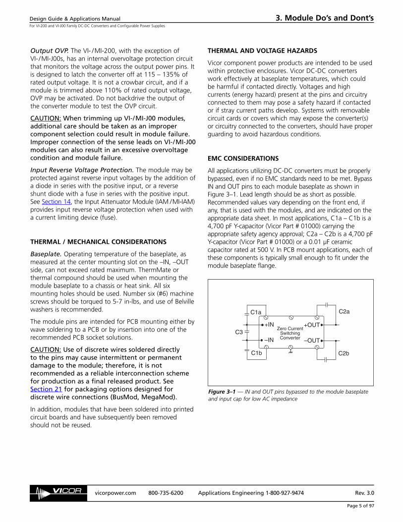
TRIMMING UP +10%
To trim 10% above the nominal output voltage, thefollowing calculations are needed to determine the valueof R8. This calculation is dependent on the output voltageof the module. A 12 V output will be used as an example.(Figure 5–3)
It is necessary for the voltage at the TRIM pin to be 10%greater than the 2.5 V reference. This offset will cause theerror amplifier to adjust the output voltage up 10% to 13.2 V.
V1 = 2.5 V + 10% = 2.75 V
IR5 = (2.75 V – 2.5 V) = 25 µA10 kΩ
Since IR5 = IR6 ,the voltage drop across R6 = (90 kΩ) (25 µA) = 2.25 V.
Therefore, V2 = 2.75 V + 2.25 V = 5 V. The currentthrough R7 (10 kΩ pot) is:
IR7 = V2 = 5 = 500 µAR7 10 k
Using Kirchoff’s current law:
IR8 = IR7 + IR6 = 525 µA
Thus, knowing the current and voltage, R8 can bedetermined:
VR8 = (Vout + 10%) – V2 = 13.2 V – 5 V = 8.2 V
R8 = (8.2 V) = 15.6 kΩ525 µA
This resistor configuration allows a 12 V output module to be trimmed up to 13.2 V and down to 10.8 V. Followthis procedure to determine resistor values for otheroutput voltages.
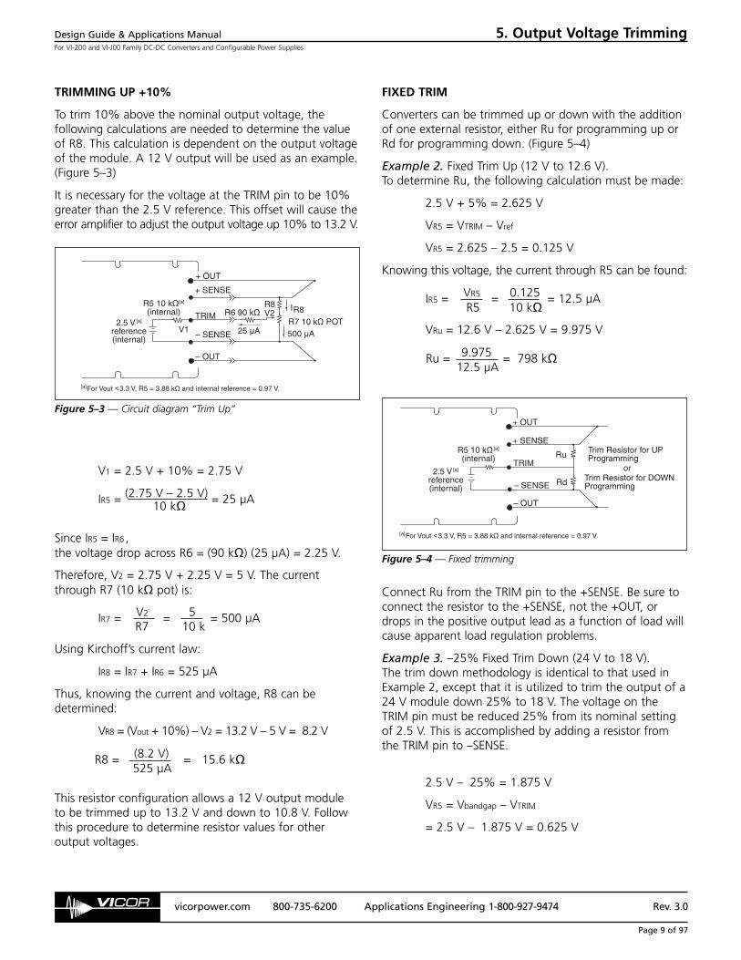
FIXED TRIM
Converters can be trimmed up or down with the additionof one external resistor, either Ru for programming up orRd for programming down. (Figure 5–4)
Example 2. Fixed Trim Up (12 V to 12.6 V). To determine Ru, the following calculation must be made:
2.5 V + 5% = 2.625 V
VR5 = VTRIM – Vref
VR5 = 2.625 – 2.5 = 0.125 V
Knowing this voltage, the current through R5 can be found:
IR5 = VR5 = 0.125 = 12.5 µAR5 10 kΩ
VRu = 12.6 V – 2.625 V = 9.975 V
Ru = 9.975 = 798 kΩ12.5 µA
Connect Ru from the TRIM pin to the +SENSE. Be sure toconnect the resistor to the +SENSE, not the +OUT, ordrops in the positive output lead as a function of load willcause apparent load regulation problems.
Example 3. –25% Fixed Trim Down (24 V to 18 V). The trim down methodology is identical to that used inExample 2, except that it is utilized to trim the output of a24 V module down 25% to 18 V. The voltage on theTRIM pin must be reduced 25% from its nominal settingof 2.5 V. This is accomplished by adding a resistor fromthe TRIM pin to –SENSE.
2.5 V – 25% = 1.875 V
VR5 = Vbandgap – VTRIM
= 2.5 V – 1.875 V = 0.625 V
IV2R6 90 kΩTRIM
+ SENSE
– SENSE
– OUT
R5 10 kΩ[a]
(internal)
V1
R8R8
R7 10 kΩ POT 500 μA 25 μA
2.5 V [a]
reference(internal)
+ OUT
[a]For Vout <3.3 V, R5 = 3.88 kΩ and internal reference = 0.97 V.
Figure 5–3 — Circuit diagram “Trim Up”
TRIM
+ OUT
+ SENSE
– SENSE
– OUT
Rd
Ru Trim Resistor for UPProgramming
Trim Resistor for DOWNProgramming
or2.5 V [a]
reference(internal)
R5 10 kΩ[a]
(internal)
[a]For Vout <3.3 V, R5 = 3.88 kΩ and internal reference = 0.97 V.
Figure 5–4 — Fixed trimming

Design Guide & Applications ManualFor VI-200 and VI-J00 Family DC-DC Converters and Configurable Power Supplies
vicorpower.com 800-735-6200 Applications Engineering 1-800-927-9474 Rev. 3.0
Page 10 of 97
Knowing this voltage, the current through R5 can be found:
IR5 = VR5 = 0.625 = 62.5 µAR5 10 kΩ
The voltage across the resistor, Rd, and the currentflowing through it are known:
Rd = (2.5 V – 0.625 V) = 30 kΩ62.5 µA
Connect Rd (Figure 5–4) from the TRIM pin to the –SENSEof the module. Be sure to connect the resistor to the–SENSE, not the –OUT, or drops in the negative outputlead as a function of load will cause apparent loadregulation problems.
DYNAMIC ADJUSTMENT PROCEDURE
Output voltage can also be dynamically programmed bydriving the TRIM pin from a voltage or current source;programmable power supplies and power amplifierapplications can be addressed in this way. For dynamicprogramming, drive the TRIM pin from a source referencedto the negative sense lead, and keep the drive voltage inthe range of 1.25 – 2.75 V. Applying 1.25 – 2.5 V on theTRIM pin corresponds to 50 – 100% of nominal outputvoltage. For example, an application requires a +10, 0%(nominal), and a –15% output voltage adjustment for a 48 Voutput converter. Referring to the table below, the voltagethat should be applied to the trim pin would be as follows:
VTRIM VOUT Change from nominal
2.125 40.8 –15%2.5 48 02.75 52.8 +10%
The actual voltage range is further restricted by theallowable trim range of the converter. Voltages in excessof 2.75 V (+10% over nominal) may cause overvoltageprotection to be activated. For applications where themodule will be programmed on a continuous basis theslew rate should be limited to 30 Hz sinusoidal.
TRIMMING ON THE WEB (VICORPOWER.COM)
Trim values are calculated automatically. DesignCalculators are available on Vicor’s website in thePowerBenchTM section at vicorpower.com/tools.
Resistor values can be easily determined for fixed trim up,fixed trim down and for variable trimming applications.
In addition to trimming information, the website alsoincludes design tips, applications circuits, EMCsuggestions, thermal design guidelines and PDF datasheets for all available Vicor products.
Percent Resistance–5 % 190 kΩ
–10 % 90 kΩ–15 % 56.7 kΩ–20 % 40 kΩ–25 % 30 kΩ–30 % 23.3 kΩ–35 % 18.6 kΩ–40 % 15 kΩ–45 % 12.2 kΩ–50 % 10 kΩ
Vnom V (Desired) Trim Resistor [a]
5 V 4.5 V 90.9 kΩ3.3 V 19.6 kΩ2.5 V 10.0 kΩ
15 V 13.8 V 115 kΩ24 V 20 V 49.9 kΩ48 V 40 V 49.9 kΩ
36 V 30.1 kΩ
Vnom V (Desired) Trim Resistor [a]
5 V 5.2 V 261 kΩ5.5 V 110 kΩ
12 V 12.5 V 953 kΩ13.2 V 422 kΩ
15 V 15.5 V 1.62 MΩ16.5 V 562 kΩ
24 V 25 V 2.24 MΩ48 V 50 V 4.74 MΩ
Table 5–1 — Values for trim down by percentage (Refer to productdata sheet for allowable trim ranges at vicorpower.com)
Values for Trim Down by Percentage
Fixed Trim Down
Table 5–2a — Values for fixed trim down by voltage
Fixed Trim Up
Table 5–2b — Values for fixed trim up by voltage
[a] Values listed in the tables are the closest standard 1% resistor values.
5. Output Voltage Trimming

Design Guide & Applications ManualFor VI-200 and VI-J00 Family DC-DC Converters and Configurable Power Supplies
vicorpower.com 800-735-6200 Applications Engineering 1-800-927-9474 Rev. 3.0
Page 11 of 97
OVERVIEW
A number of GATE IN pins may be connected for remoteshut down and logic disable. (Figure 6-1) Diodes D1 andD2 provide isolation and prevent multiple failures if theGATE IN of a module becomes shorted to the +IN. TheZener diodes Z1, Z2 and capacitors C1, C2 attenuatetransient voltage spikes caused by differential inductancein the negative lead. Capacitors C1 and C2 will also
lengthen turn-on time. SW1 is a mechanical or solid stateswitch that is used to disable both Driver modules. C3 isused to minimize the effects of “switch bounce” associatedwith mechanical devices.
NOTE: GATE IN voltage needs to be <0.65 Vreferenced to –IN to ensure modules are disabled.
+IN
–IN
GATEOUT
GATEIN
+IN
–IN
GATEOUT
GATEIN
VicorDC-DC Converter
F1
C1Z1
C3
SW1 F2
DISABLE
D2
Z2 C2
D1
VicorDC-DC Converter
6. Multiple GATE IN Connections
C1, C2, C3 = 1 µFZ1, Z2 = 15 V (1N5245B)D1, D2 = Small signal diode (1N4148)
[a]
[a]For bus voltages greater than 75 V, a 1N4006 diode should be used.
NOTE: The –IN to –IN input lead should be kept as short as possible to minimize differential inductance.
Heavy lines indicate power connections. Use suitably sized conductors.
Opto-couplers or relays should be used to isolate GATE IN connections, if the converters are on separate boards or the negative input lead’s impedance is high.
Figure 6–1 — Protection for multiple GATE IN connections

Design Guide & Applications ManualFor VI-200 and VI-J00 Family DC-DC Converters and Configurable Power Supplies
vicorpower.com 800-735-6200 Applications Engineering 1-800-927-9474 Rev. 3.0
Page 12 of 97
Logic Disable. (Figure 7–1) The GATE IN pin of themodule may be used to turn the module on or off. WhenGATE IN is pulled low (<0.65 V @ 6 mA, referenced to–Vin), the module is turned off. When GATE IN is floating(open collector), the module is turned on. The open circuitvoltage of the GATE IN pin is less than 10 V. This appliesto VI-/MI-200, VI-/MI-J00 and MegaMod / MI-MegaModFamily modules.
Output Voltage Programming. (Figure 7–2) ConsultVicor’s Applications Engineering Department beforeattempting large signal applications at high repetitionrates due to ripple current considerations with the internaloutput capacitors. This applies to VI-/MI-200, VI-/MI-J00,ComPAC/MI-ComPAC, FlatPAC and MegaMod /MI-MegaMod Family modules.
Vout = Vtrim x Vnom2.5
Negative Inputs (with positive ground). (Figure 7–3)Vicor modules have isolated inputs and outputs makingnegative input configurations easy. Fusing should alwaysbe placed in the positive lead.
Remote Sensing. (Figure 7–4) Output voltage between+OUT and –OUT must be maintained below 110% ofnominal. Do not exceed 0.25 V drop in negative return asthe current limit setpoint is moved out proportionately.The sense should be closed at the module if remotesensing is not desired. Applies to VI-/MI-200, VI-/MI-J00,ComPAC/MI-ComPAC, FlatPAC and MegaMod /MI-MegaMod Family modules. Excessively long sense leadsand / or excessive external capacitance at the load mayresult in module instability. Please consult VicorApplications Engineering for compensation methods.
–OUT
–S
+S
+OUT+IN
GATEIN
GATEOUT–IN
Zero CurrentSwitchingConverter
Driver
+–
16
TLP798GAgilent 6N139
Load25
TRIM1µF
7. Application Circuits / Converter Array Design Considerations
Figure 7–1 — Logic disable
–OUT
–STRIM
+S
+OUT+IN
GATEIN
GATEOUT–IN
Zero CurrentSwitchingConverter
Driver
+– Load
+–
Figure 7–2 — Output voltage programming
–OUT
–S
TRIM
+S
+OUT+IN
GATEIN
GATEOUT
–IN
Zero CurrentSwitchingConverter
Driver
+– Load
Figure 7–3 — Negative inputs (with positive ground)
–OUT
–S
TRIM
+S
+OUT+IN
GATE IN
GATEOUT–IN
Zero CurrentSwitchingConverter
Driver
+– Load
• • •• • •
• • •• • •
• • •• • •
• • •• • •
Figure 7–4 — Remote sensing

Design Guide & Applications ManualFor VI-200 and VI-J00 Family DC-DC Converters and Configurable Power Supplies
vicorpower.com 800-735-6200 Applications Engineering 1-800-927-9474 Rev. 3.0
Page 13 of 97
Parallel Boost. (Figure 7–5) U.S. Patent #4,648,020 —other patents pending. To retain accurate power sharingbetween a Driver and (n) number of Boosters, provideadequate input and output power bussing. This applies toVI-/MI-200 and MegaMod / MI-MegaMod Familymodules. See Module Do’s and Don’ts for recommendedexternal components. (Section 3)
Programmable Current Source. (Figure 7–6) Moduleoutput voltage should not exceed the rated voltage of theoperational amplifier. This applies to VI-/MI-200, VI-/MI-J00, ComPAC/ MI-ComPAC, FlatPAC andMegaMod / MI-MegaMod Family modules.
NOTE: When using a VI-J00 module, the TRIM pinvoltage should be clamped to 2.75 V to avoiddamage to the module. This corresponds to themaximum trim up voltage. This circuit or functionalequivalent must be used when charging batteries. Do not exceed the nominal current ratings of theconverter. Example,
Pout
Vnominal
Dual Output Voltages. (Figure 7–7) Vicor modules haveisolated outputs so they can easily be referenced to acommon node creating positive and / or negative rails.
7. Application Circuits / Converter Array Design Considerations
Figure 7–5 — Parallel boost. U.S. Patent #4,648,020 — otherpatents pending.
–OUT
–S
TRIM
+S
+OUT+IN
GATEIN
GATEOUT
–IN
Zero CurrentSwitchingConverter
#1Driver
VI-2xx-xx
+–
–OUT
–S
TRIM
+S
+OUT+IN
GATEIN
GATEOUT
–IN
Zero CurrentSwitchingConverter
#nBooster
VI-Bxx-xx
Load
Figure 7–6 — Programmable current source
–OUT
-STRIM
+S
+OUT+IN
GATEIN
GATEOUT–IN
Zero CurrentSwitchingConverter
Driver
+– Load
V Control0.1 V/A
1K OPAMP
–
+
1K 1K
0.05 Ω
1K0.01
I
10 μF
–OUT
–S
TRIM
+S
+OUT+IN
GATEIN
GATEOUT–IN
Zero CurrentSwitchingConverter
Driver
+–
Load requiringpositive output
–OUT
–STRIM
+S
+OUT+IN
GATEIN
GATEOUT
–IN
Zero CurrentSwitchingConverter
Driver
+–
Load requiringnegative output
Figure 7–7 — Dual output voltages
Design Guide & Applications ManualFor VI-200 and VI-J00 Family DC-DC Converters and Configurable Power Supplies
vicorpower.com 800-735-6200 Applications Engineering 1-800-927-9474 Rev. 3.0
Page 14 of 97
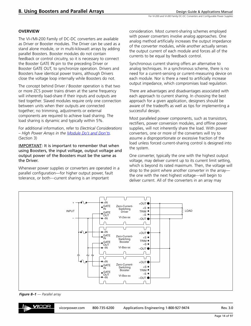
OVERVIEW
The VI-/MI-200 Family of DC-DC converters are availableas Driver or Booster modules. The Driver can be used as astand alone module, or in multi-kilowatt arrays by addingparallel Boosters. Booster modules do not containfeedback or control circuitry, so it is necessary to connectthe Booster GATE IN pin to the preceding Driver orBooster GATE OUT, to synchronize operation. Drivers andBoosters have identical power trains, although Driversclose the voltage loop internally while Boosters do not.
The concept behind Driver / Booster operation is that twoor more ZCS power trains driven at the same frequencywill inherently load-share if their inputs and outputs aretied together. Slaved modules require only one connectionbetween units when their outputs are connectedtogether; no trimming, adjustments or externalcomponents are required to achieve load sharing. Theload sharing is dynamic and typically within 5%.
For additional information, refer to Electrical Considerations– High Power Arrays in the Module Do’s and Don’ts.(Section 3)
IMPORTANT: It is important to remember that whenusing Boosters, the input voltage, output voltage andoutput power of the Boosters must be the same asthe Driver.
Whenever power supplies or converters are operated in aparallel configuration—for higher output power, faulttolerance, or both—current sharing is an important
consideration. Most current-sharing schemes employedwith power converters involve analog approaches. Oneanalog method artificially increases the output impedanceof the converter modules, while another actually sensesthe output current of each module and forces all of thecurrents to be equal by feedback control.
Synchronous current sharing offers an alternative toanalog techniques. In a synchronous scheme, there is noneed for a current-sensing or current-measuring device oneach module. Nor is there a need to artificially increaseoutput impedance, which compromises load regulation.
There are advantages and disadvantages associated witheach approach to current sharing. In choosing the bestapproach for a given application, designers should beaware of the tradeoffs as well as tips for implementing asuccessful design.
Most paralleled power components, such as transistors,rectifiers, power conversion modules, and offline powersupplies, will not inherently share the load. With powerconverters, one or more of the converters will try toassume a disproportionate or excessive fraction of theload unless forced current-sharing control is designed intothe system.
One converter, typically the one with the highest outputvoltage, may deliver current up to its current limit setting,which is beyond its rated maximum. Then, the voltage willdrop to the point where another converter in the array—the one with the next highest voltage—will begin todeliver current. All of the converters in an array may
Figure 8–1 — Parallel array
INPUT LOAD+S
TRIM–S
–OUT
+INGATEINGATEOUT–IN
+STRIM
–S
–OUT
+INGATEINGATEOUT–IN
+STRIM
–S
–OUT
+INGATEINGATEOUT–IN
+
–
Zero-Current-Switching
Driver
VI-2xx-xx
Zero-Current-SwitchingBooster
VI-Bxx-xx
Zero-Current-SwitchingBooster
VI-Bxx-xx
+OUT
+OUT
+OUT
8. Using Boosters and Parallel Arrays

Design Guide & Applications ManualFor VI-200 and VI-J00 Family DC-DC Converters and Configurable Power Supplies
vicorpower.com 800-735-6200 Applications Engineering 1-800-927-9474 Rev. 3.0
Page 15 of 97
deliver some current, but the load will be shared unequally.With built-in current limiting, one or more of the converterswill deliver current up to the current limit (generally 15 or20% above the module’s rated maximum), while otherconverters in the array supply just a fraction of load.
Consider a situation where one module in a two-modulearray is providing all of the load. If it fails, the load on thesecond module must go from no load to full load. Duringthat time, the output voltage is likely to droop temporarily.This could result in system problems, including shutdownor reset.
On the other hand, if both modules were sharing the loadand one failed, the surviving module would experience amuch less severe transient (one-half to full load). Also, theoutput voltage would be likely to experience no morethan a slight momentary droop. The dynamic responsecharacteristic of all forward converters, resonant or pulse-width modulated, is degraded when the load is steppedfrom zero (no load) where the output inductor current isdiscontinuous.
In the same two-module array example, the modulecarrying all of the load also is generating all of the heat.That results in a much lower mean time between failurefor that module. An often-quoted rule of thumb says thatfor each 10°C increase in operating temperature, averagecomponent life is cut in half.
In a current-sharing system, the converters or supplies allrun at the same temperature. This temperature is lowerthan that of the hot-running (heavily loaded) modules in a system without current sharing. Furthermore, same-temperature operation means that all of the modules in a current-sharing arrangement age equally.
Current sharing, then, is important because it improvessystem performance. It optimizes transient and dynamicresponse and minimizes thermal problems, which improvesreliability and helps extend the lifetimes of all of themodules in an array. Current sharing is an essentialingredient in most systems that use multiple power suppliesor converters to achieve higher output power or faulttolerance.
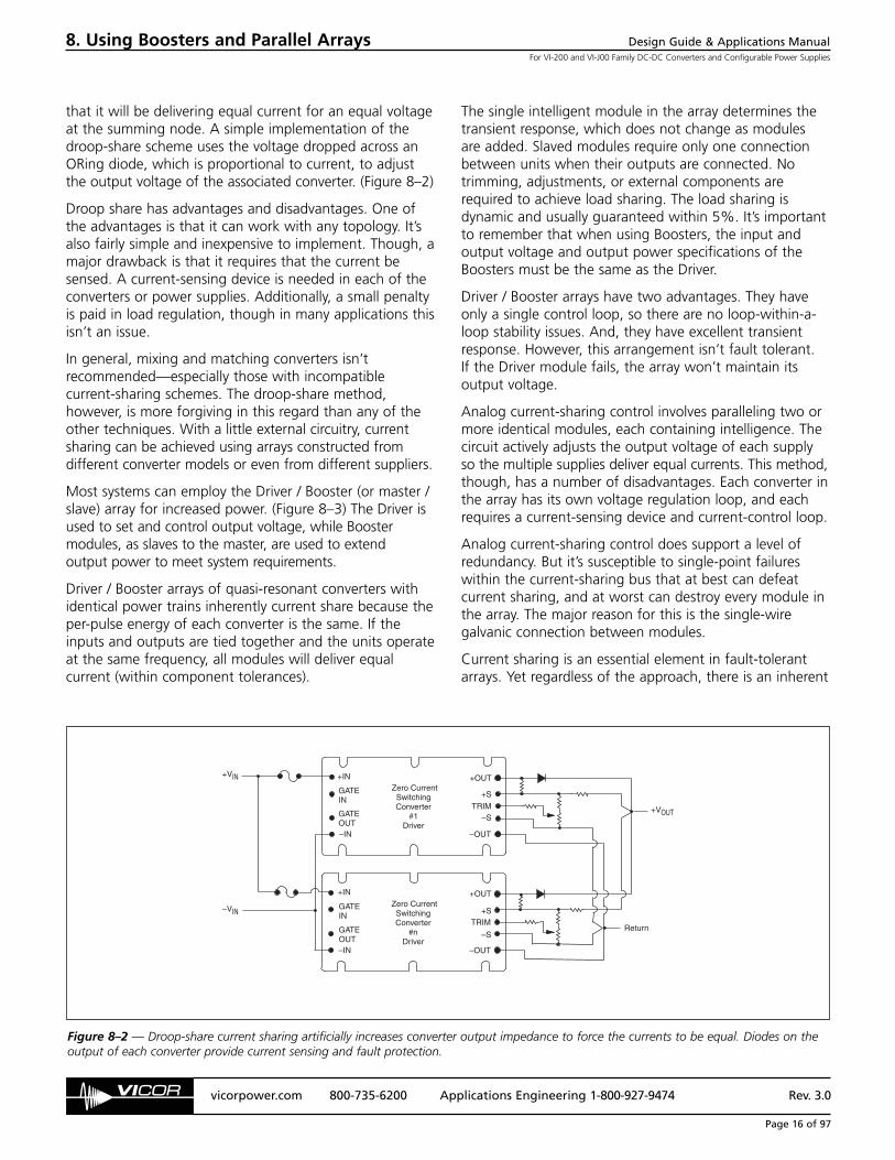
When parallel supplies or converters are used to increasepower, current sharing is achieved through a number ofapproaches. One scheme simply adds resistance in serieswith the load. A more practical variant of that is the“droop-share” method, which actively causes the outputvoltage to drop in response to increasing load.Nevertheless, the two most commonly used approaches to paralleling converters for power expansion are Driver /Booster arrays and analog current-sharing control. Theyappear to be similar, but the implementation of each isquite different.
Driver / Booster arrays usually contain one intelligentmodule or Driver, and one or more power-train-onlymodules or Boosters. Analog current-sharing controlinvolves paralleling two or more identical modules, eachcontaining intelligence.
One of the common methods of forcing load sharing inan array of parallel converters is to sense the outputcurrent of each converter and compare it to the averagecurrent. Then, the output of a given converter is adjustedso that its contribution is equal to the average. This isusually accomplished by current-sense resistors in serieswith the load, a sensing amplifier for each convertermodule, and a summing amplifier. Load sharing isaccomplished by actively trimming the output voltageusing TRIM or SENSE pins.
Occasionally, a designer is tempted to avoid the expenseof a current-sense resistor by using the IR drops in thewire as a means of sensing the current. Unfortunately,there are a number of negative issues associated with that idea. First of all, there’s the temperature coefficient of copper. As the wire heats up, its resistance increases,negating its value as a stable current-sensing device.Second, there are oxidation and corrosion issues, whichalso cause parametric changes. Consequently, a high-precision current-sensing device, such as a precisionresistor, is a must.
The resistor values typically range from a few milliohms up to about 100 mΩ, depending on the power level orcurrent range of operation. Selecting the right valuerequires a tradeoff between power dissipation andsensitivity (signal-to-noise ratio or noise immunity). Thelarger the resistor value, the better the noise immunity—and the greater the power dissipation.
Determining the size of the resistor needed to generate asignal above the noise can be a bit tricky. Anotherpotential pitfall with this (or, for that matter, any other)approach is the need for good electrical and mechanicaldesign and layout. This requires adequate trace widths,minimized trace lengths, and decoupling to reduce noise.An experienced designer should have no difficulty withthis, but it is an area rich with opportunities for error.
The droop-share method artificially increases the outputimpedance to force the currents to be equal. It’s accomplished by injecting an error signal into thecontrol loop of the converter, causing the output voltageto vary as a function of load current. As load currentincreases, output voltage decreases. All of the moduleswill deliver approximately the same current because theyare all being summed into one node.
If one supply is delivering more current than anothersupply, its output voltage will be slightly forced down so
8. Using Boosters and Parallel Arrays
Design Guide & Applications ManualFor VI-200 and VI-J00 Family DC-DC Converters and Configurable Power Supplies
vicorpower.com 800-735-6200 Applications Engineering 1-800-927-9474 Rev. 3.0
Page 16 of 97
that it will be delivering equal current for an equal voltageat the summing node. A simple implementation of thedroop-share scheme uses the voltage dropped across anORing diode, which is proportional to current, to adjustthe output voltage of the associated converter. (Figure 8–2)
Droop share has advantages and disadvantages. One ofthe advantages is that it can work with any topology. It’salso fairly simple and inexpensive to implement. Though, amajor drawback is that it requires that the current besensed. A current-sensing device is needed in each of theconverters or power supplies. Additionally, a small penaltyis paid in load regulation, though in many applications thisisn’t an issue.
In general, mixing and matching converters isn’trecommended—especially those with incompatiblecurrent-sharing schemes. The droop-share method,however, is more forgiving in this regard than any of theother techniques. With a little external circuitry, currentsharing can be achieved using arrays constructed fromdifferent converter models or even from different suppliers.
Most systems can employ the Driver / Booster (or master /slave) array for increased power. (Figure 8–3) The Driver isused to set and control output voltage, while Boostermodules, as slaves to the master, are used to extend output power to meet system requirements.
Driver / Booster arrays of quasi-resonant converters withidentical power trains inherently current share because theper-pulse energy of each converter is the same. If theinputs and outputs are tied together and the units operateat the same frequency, all modules will deliver equalcurrent (within component tolerances).
The single intelligent module in the array determines thetransient response, which does not change as modules are added. Slaved modules require only one connectionbetween units when their outputs are connected. Notrimming, adjustments, or external components arerequired to achieve load sharing. The load sharing isdynamic and usually guaranteed within 5%. It’s importantto remember that when using Boosters, the input andoutput voltage and output power specifications of theBoosters must be the same as the Driver.
Driver / Booster arrays have two advantages. They haveonly a single control loop, so there are no loop-within-a-loop stability issues. And, they have excellent transientresponse. However, this arrangement isn’t fault tolerant. If the Driver module fails, the array won’t maintain itsoutput voltage.
Analog current-sharing control involves paralleling two ormore identical modules, each containing intelligence. Thecircuit actively adjusts the output voltage of each supplyso the multiple supplies deliver equal currents. This method,though, has a number of disadvantages. Each converter inthe array has its own voltage regulation loop, and eachrequires a current-sensing device and current-control loop.
Analog current-sharing control does support a level ofredundancy. But it’s susceptible to single-point failureswithin the current-sharing bus that at best can defeatcurrent sharing, and at worst can destroy every module inthe array. The major reason for this is the single-wiregalvanic connection between modules.
Current sharing is an essential element in fault-tolerantarrays. Yet regardless of the approach, there is an inherent
–OUT
–STRIM
+S
+OUT+IN
GATEIN
GATEOUT–IN
–OUT
–S
TRIM+S
+OUT+IN
GATEIN
GATEOUT–IN
Return
Zero CurrentSwitchingConverter
#1Driver
Zero CurrentSwitchingConverter
#nDriver
+VIN
+VOUT
–VIN
Figure 8–2 — Droop-share current sharing artificially increases converter output impedance to force the currents to be equal. Diodes on theoutput of each converter provide current sensing and fault protection.
8. Using Boosters and Parallel Arrays

Design Guide & Applications ManualFor VI-200 and VI-J00 Family DC-DC Converters and Configurable Power Supplies
vicorpower.com 800-735-6200 Applications Engineering 1-800-927-9474 Rev. 3.0
Page 17 of 97
cost incurred by the addition of at least one redundantconverter or supply.
Incidentally, most applications today that require faulttolerance or redundancy also require Hot-Swap capabilityto ensure continuous system operation. Hot-swappablecards must be designed so the operator won’t come incontact with dangerous potentials and currents.
It’s also essential that when a module fails, the failure isdetected and identified by an alarm or notice to provideservice. A Hot-Swap system must ensure that duringswap-out, there is minimal disturbance of the power bus.Specifically, the affected voltage bus must not dropenough to cause errors in the system, either on the inputbus or the output bus.
A power-supply failure can cripple an entire system, so theaddition of a redundant converter or supply is oftenjustified by the need to keep the system operating.Adding an extra module (N+1) to a group of paralleledmodules will significantly increase reliability with only amodest increase in cost.
The implementation of redundant converters isdetermined in part by the available space and costrequirements. For example, two 200 W full-size modules
could be used to provide a 400 W output with anadditional 200 W module for 2+1 redundancy (a total of600 W in a volume of about 16.5 in3).
Alternatively, four 100 W half-size modules might be usedwith a fifth 100 W module to provide 4+1 redundancy (atotal of 500 W and 14 in3). Although the second solutionuses less space, it increases the accumulated failure ratebecause it employs more converters, more ORing diodes,more monitoring circuitry, and more assembly.
ORing diodes may be inserted in series with the output of each module in an N+1 array to provide output faulttolerance. (Figure 8–2) They’re important in a redundantpower system to maintain fault isolation. Without them, a short-circuit failure in the output of one converter couldbring down the entire array.
But ORing diodes add losses to the power system,reducing overall efficiency and decreasing reliability. Toameliorate the negative effect on efficiency, ORing diodesshould run hot, thereby reducing forward voltage dropand increasing efficiency. Reverse leakage current will bean issue only if the output of a converter shorts and thediode is reverse biased. This is an important considerationwith regard to operating temperature.
8. Using Boosters and Parallel Arrays
INPUT LOAD+ Sense
Trim
–Sense
GATEIN
–IN
Zero-Current-Switching Driver
+OUT
GATEOUT
+IN
–OUT
+Sense
Trim
–Sense
–IN
Zero-Current-Switching Booster
+OUT+IN
–OUT
+Sense
Trim
–Sense
–IN
Zero-Current-Switching Booster
+OUT+IN
–OUT
+VIN
-VIN
GATEIN
GATEOUT
GATEIN
GATEOUT
Figure 8–3 — Most converters can use the Driver / Booster array to increase output power. Driver / Booster arrays usually contain oneintelligent module or Driver, and one or more power-train-only modules or Boosters.
Design Guide & Applications ManualFor VI-200 and VI-J00 Family DC-DC Converters and Configurable Power Supplies
vicorpower.com 800-735-6200 Applications Engineering 1-800-927-9474 Rev. 3.0
Page 18 of 97
+IN
GATEINGATEOUT–IN
+OUT
+STRIM
–S–OUT
C2
C1
C2 C3
C3
C1 = 100 μF C2 = 4,700 pF C3 = 0.01 μF
Conditions: Light Load = 3 A Nominal Line = 48 V Nominal Load = 15 A Full Load = 30 A
Figure 9–1 — Conducted input noise, no additional filtering
3 Amp Load 15 Amp Load 30 Amp Load
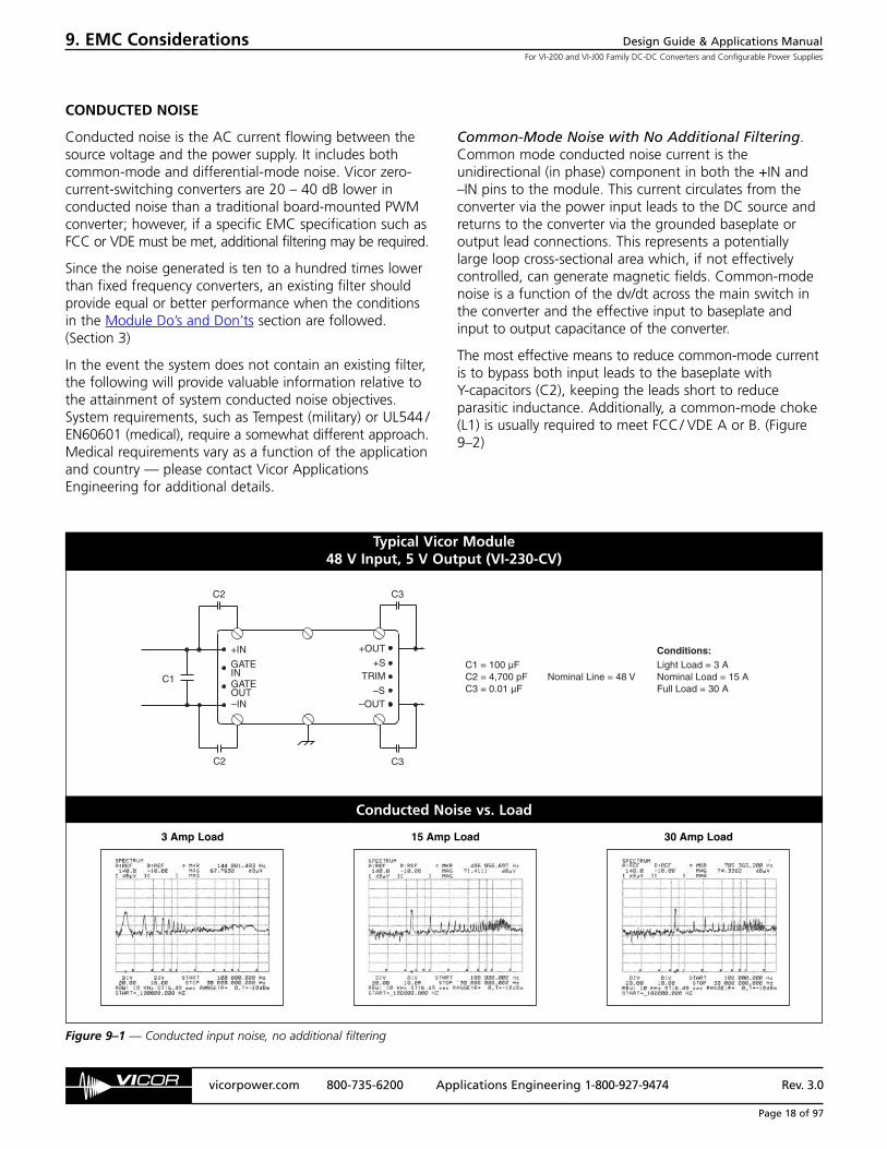
CONDUCTED NOISE
Conducted noise is the AC current flowing between thesource voltage and the power supply. It includes bothcommon-mode and differential-mode noise. Vicor zero-current-switching converters are 20 – 40 dB lower inconducted noise than a traditional board-mounted PWMconverter; however, if a specific EMC specification such asFCC or VDE must be met, additional filtering may be required.
Since the noise generated is ten to a hundred times lowerthan fixed frequency converters, an existing filter shouldprovide equal or better performance when the conditionsin the Module Do’s and Don’ts section are followed.(Section 3)
In the event the system does not contain an existing filter,the following will provide valuable information relative tothe attainment of system conducted noise objectives.System requirements, such as Tempest (military) or UL544 /EN60601 (medical), require a somewhat different approach.Medical requirements vary as a function of the applicationand country — please contact Vicor ApplicationsEngineering for additional details.
Common-Mode Noise with No Additional Filtering.Common mode conducted noise current is theunidirectional (in phase) component in both the +IN and–IN pins to the module. This current circulates from theconverter via the power input leads to the DC source andreturns to the converter via the grounded baseplate oroutput lead connections. This represents a potentiallylarge loop cross-sectional area which, if not effectivelycontrolled, can generate magnetic fields. Common-modenoise is a function of the dv/dt across the main switch inthe converter and the effective input to baseplate andinput to output capacitance of the converter.
The most effective means to reduce common-mode currentis to bypass both input leads to the baseplate with Y-capacitors (C2), keeping the leads short to reduceparasitic inductance. Additionally, a common-mode choke(L1) is usually required to meet FCC/ VDE A or B. (Figure9–2)
9. EMC Considerations
Conducted Noise vs. Load
Typical Vicor Module48 V Input, 5 V Output (VI-230-CV)

Design Guide & Applications ManualFor VI-200 and VI-J00 Family DC-DC Converters and Configurable Power Supplies
vicorpower.com 800-735-6200 Applications Engineering 1-800-927-9474 Rev. 3.0
Page 19 of 97
9. EMC Considerations
Common-Mode Noise with Common-Mode Choke.There are no special precautions that must be exercised inthe design of input filters for Vicor converters. In fact, ifthe system contains an EMC filter designed for typicalfixed frequency converters, it should be sufficient as is(although not optimal in terms of size), as zero-current-switching converters inherently generate significantly lessconducted noise.
The plots in Figure 9–2 are representative of fixedfrequency converters with input filtering.
NOTE: In most cases, a fixed frequency convertergenerates more input conducted noise with a filterthan Vicor’s zero-current-switching converter withouta filter. Also note that fixed frequency convertersusing a construction technique involving controlcircuitry on the same metal plate as power processingcomponents will generate significantly more inputnoise than shown.
+IN
–IN+OUT
–OUT
C1 = 2.2 μFC2 = 100 μFC3 = InternalC4 = InternalL1 = 3 mH
Conditions:Light Load = 3 ANominal Load = 15 AFull Load = 30 A
C1
L1
C2
C3
C3
C4
C4
Nominal Line = 48 V
Figure 9–2 — Conducted input noise, typical fixed frequency converter with filter
3 Amp Load 15 Amp Load 30 Amp Load
Typical Fixed Frequency Converter (PWM)48 V Input, 5 V Output
Conducted Noise vs. Load

Design Guide & Applications ManualFor VI-200 and VI-J00 Family DC-DC Converters and Configurable Power Supplies
vicorpower.com 800-735-6200 Applications Engineering 1-800-927-9474 Rev. 3.0
Page 20 of 97
9. EMC Considerations
L1
C4
C1 = 100 μF
C2a – C2b = 4,700 pF (Vicor Part # 01000)
C3a – C3b = 0.01 μF (Vicor Part # 04872)
C4 = 2.2 μF
L1 = 3,000 μH (Vicor Part # 31742)
Conditions
Light Load = 3 A
Nominal Load = 15 A
Full Load = 30 A
+IN
GATEINGATEOUT–IN
+OUT
+STRIM
–S–OUT
C2a
C1
C2b C3b
C3a
3 Amp Load 15 Amp Load 30 Amp Load
Conducted Noise vs. Load
Figure 9–3 — Conducted input noise, with common-mode choke
Typical Vicor Module (VI-230-CV)48 V Input, 5 V Output
Three common-mode chokes are offered as standard accessories.
NOTE: Common-mode filters may be common to one or more modules, but only one should be used with modulesinterconnected via GATE IN’s or, GATE OUT to GATE IN. As an example, Driver / Booster arrays or Drivers with GATE IN’s tied together to provide a common disable function.
Part Inductance Maximum ResistanceNumber Each Winding DC Current Each Winding31743 1,000 µH 12 Amperes 6.5 mΩ31742 3,000 µH 7 Amperes 18 mΩ31943 2,163 µH 1 Ampere 42 mΩ

Design Guide & Applications ManualFor VI-200 and VI-J00 Family DC-DC Converters and Configurable Power Supplies
vicorpower.com 800-735-6200 Applications Engineering 1-800-927-9474 Rev. 3.0
Page 21 of 97
9. EMC Considerations
Differential and Common-Mode Filter with Morethan One Module. No special precautions are neededwhen using two or more modules. The filter required willhave the same characteristics as a single module filter,
however the wire size on the magnetics will need toreflect the increased input current. Shown below is theinput conducted noise for two modules sharing acommon input source.
+IN
GATEINGATEOUT–IN
+OUT
+S
T–S
–OUT
Load 1
Load 2
L2
C4
L1
C1a
C2a
C2d
C2c
C2b
C3a
C3b
C3c
C3d
C1b
+IN
GATEINGATEOUT–IN
+OUT
+S
T–S
–OUT
C1a – C1b = 47 μF C2a – C2d = 4,700 pF (Vicor Part # 01000) C3a – C3d = 0.01 μF (Vicor Part # 04872) C4 = 2.2 μF L1 = 3,000 μH (Vicor Part # 31742) L2 = 20 μH
ConditionsLight Load = 3 ANominal Load = 15 AFull Load = 30 A
Figure 9–4 — Conducted noise, multiple zero-current-switching converters
3 Amp / 3 Amp Load 3 Amp / 6 Amp Load
15 Amp / 15 Amp Load
3 Amp / 30 Amp Load
15 Amp / 30 Amp Load 30 Amp / 30 Amp Load
Differential and Common-Mode Filter with More than One Module48 V Inputs, 5 V Outputs (Two Vicor VI-230-CV Modules)
Conducted Noise vs. Load
Three common-mode chokes are offered as standard accessories.
NOTE: Common-mode filters may be common to one or more modules, but only one should be used with modulesinterconnected via GATE IN’s or, GATE OUT to GATE IN. As an example, Driver / Booster arrays or Drivers with GATE IN’s tied together to provide a common disable function.
Part Inductance Maximum ResistanceNumber Each Winding DC Current Each Winding31743 1,000 µH 12 Amperes 6.5 mΩ31742 3,000 µH 7 Amperes 18 mΩ31943 2,163 µH 1 Ampere 42 mΩ
Design Guide & Applications ManualFor VI-200 and VI-J00 Family DC-DC Converters and Configurable Power Supplies
vicorpower.com 800-735-6200 Applications Engineering 1-800-927-9474 Rev. 3.0
Page 22 of 97
3 Amp Load 15 Amp Load 30 Amp Load
9. EMC Considerations
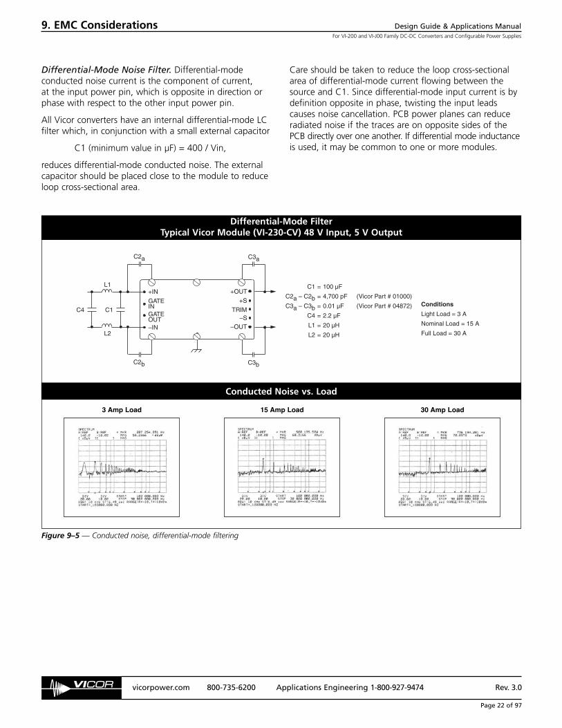
Differential-Mode Noise Filter. Differential-modeconducted noise current is the component of current, at the input power pin, which is opposite in direction orphase with respect to the other input power pin.
All Vicor converters have an internal differential-mode LCfilter which, in conjunction with a small external capacitor
C1 (minimum value in µF) = 400 / Vin,
reduces differential-mode conducted noise. The externalcapacitor should be placed close to the module to reduceloop cross-sectional area.
Care should be taken to reduce the loop cross-sectionalarea of differential-mode current flowing between thesource and C1. Since differential-mode input current is bydefinition opposite in phase, twisting the input leadscauses noise cancellation. PCB power planes can reduceradiated noise if the traces are on opposite sides of thePCB directly over one another. If differential mode inductanceis used, it may be common to one or more modules.
C2a
C1
C2b C3b
C3a
L1
C4
L2
C1 = 100 µF
C2a – C2b = 4,700 pF (Vicor Part # 01000)
C3a – C3b = 0.01 µF (Vicor Part # 04872)
C4 = 2.2 µF
L1 = 20 µH
L2 = 20 µH
+IN
GATEINGATEOUT–IN
+OUT
+S
TRIM–S
–OUT
Conditions
Light Load = 3 A
Nominal Load = 15 A
Full Load = 30 A
Figure 9–5 — Conducted noise, differential-mode filtering
Conducted Noise vs. Load
Differential-Mode FilterTypical Vicor Module (VI-230-CV) 48 V Input, 5 V Output

Design Guide & Applications ManualFor VI-200 and VI-J00 Family DC-DC Converters and Configurable Power Supplies
vicorpower.com 800-735-6200 Applications Engineering 1-800-927-9474 Rev. 3.0
Page 23 of 97
9. EMC Considerations
RADIATED NOISE
Radiated noise may be either electric field or magneticfield. Magnetic radiation is caused by high di/dt and isgenerally what is measured by FCC, VDE or MIL-STD-461.Vicor converters utilize zero-current-switching, with theadvantage over PWM non-zero-current-switching beingthat zero-current-switching topologies contain minimaldiscontinuities in the switched current waveforms,resulting in lower di/dt’s. Electric field radiation (caused bydv/dt) is “near-field,” i.e., it decays rapidly as a function ofdistance and as a result does not typically affect radiatedmeasurements.
Radiation can be minimized by proper board layout. Keepall leads with AC current short, twisted or routed asoverlapping planes to minimize loop cross-sectional area.
Also keep in mind the effects of capacitive coupling —even when not expected. Do not put an unshielded filteron the opposite side of the PCB from the module.Conducted noise can be capacitively coupled around thefilter. Do not route input and output leads in the samecable bundle. Again, no special precautions, just gooddesign practice.
NOISE CONSIDERATIONS
All switchmode power supplies generate a certain amountof “noise”, yet it remains one of the least understoodparameters in power conversion.
VI-200s and VI-J00s both use the same topology, so theiroperation is very similar. These products are zero-current-switching converters — i.e., the current is zero when themain switch is turned on or off. While the switch is on,the current through the switch or the primary of thetransformer is a half-wave rectified sine wave. Similar inoperation to a resonant converter, these products arecommonly referred to as quasi-resonant converters. TheLC resonant frequency is fixed so the on-time of theswitch is about 500 ns. When the switch turns on, energybuilds up in the leakage inductance of the transformer (L)and then “transferred” into the capacitor on thesecondary side of the module. (C, Figure 9–6) The energyprocessed in each pulse is fixed, and is ultimately theenergy stored in this capacitor, 1/2 CV2. Since the energyin every pulse is fixed, the repetition rate of the pulse trainis varied as a function of load to regulate the outputvoltage. Maximum repetition rate occurs at minimum line,full load and is approximately twice the LC time period or1 µs. If the load drops by 50%, then the repetition rate isapproximately one-half of maximum (since the energy inevery pulse is fixed). Therefore the pulse repetition ratevaries linearly with load, to a first order approximation.
Since the energy in every pulse is related to the square ofthe applied voltage (CV2), the pulse repetition rate variesas approximately the square of the line voltage. Forexample, a 300 V input unit can vary from 200 – 400 V,or a factor of two, therefore it follows that the repetitionrate must vary by approximately a factor of four to regulatethe output. As previously established, the current in theprimary is a half-wave rectified sine wave, but the voltageon the primary is a square wave. Since this voltage is asquare wave, it contains harmonics of the fundamentalswitching frequency. It also includes frequencies, that extendto 70 MHz.
These frequencies can be of interest in the followingcircumstances. Rapidly changing voltages (high dv/dt) cangenerate E-fields (primarily near-field) which do not usuallycause system noise problems since they significantlydecrease as a function of distance. For this reason, E-fieldsare not measured by agencies such as the FCC or VDE.These agencies do, however, measure the magneticradiation caused by high frequency currents in a conductor.The half-wave rectified sine wave in the transformer is anexample of this, but since there are minimal discontinuitiesin the current waveform and the loop cross-sectional areais very small, the resultant E-field is very small. E-fields canbe a problem if sensitive circuitry is located near themodule. In this case, a shield can be positioned under thelabel side of the module as a discrete element or as aground plane on the PCB. The other effect that occurs asa result of the 50 – 70 MHz component on the mainswitch is common-mode noise. (Figure 9–7)
L
C
Vs
Ip
+IN
–IN
Vp
+ OUT
–OUT
Figure 9–6 — Basic zero-current-switching converter topology (VI-200 / VI-J00)
Ceramic
ParasiticCapacitance
Baseplate
Rectifier
Ceramic
FET
ShieldShield
Figure 9–7 — The shield layer serves to reduce the capacitance

Design Guide & Applications ManualFor VI-200 and VI-J00 Family DC-DC Converters and Configurable Power Supplies
vicorpower.com 800-735-6200 Applications Engineering 1-800-927-9474 Rev. 3.0
Page 24 of 97
C FET CRectifier
ICM
CFET CRectifier
CExternal CExternal
ICM
Primary Secondary
Vp
Vp
Vp
Baseplate
I DM
Ycaps Ycaps
Figure 9–8 — Noise coupling model
9. EMC Considerations
To Scope
Ground Ring on Probe
To Scope
or
Insert probe into female receptacle(Vicor P/N 06207) for proper output differential noise measurement technique
Figure 9–9 — Output ripple measurement technique
The dv/dt of the switch (FET) is a noise generator. This FET is mounted on a two layer insulating and shieldingassembly which is attached to the baseplate. Since ceramicis a dielectric, there is capacitance from the FET to thebaseplate. (Figure 9–7) The output rectifiers are also tiedto the baseplate with ceramic insulators, adding additionalcapacitance. The dv/dt of the FET is differentiated by thesetwo series capacitors, resulting in a spike of noise currentat 50 – 70 MHz that flows from primary to secondary.(Figure 9–8) This noise current is common-mode as opposedto differential, and therefore should not affect the operationof the system. It should be noted, however, that oscilloscopeshave a finite ability to reject common-mode signals, andthese signals can be abnormally emphasized by the use oflong ground leads on the scope probe.
MEASURING OUTPUT NOISE
Long ground leads adversely impact the common-moderejection capability of oscilloscopes because the groundlead has inductance not present on the signal lead. Thesediffering impedances take common-mode signals andconvert them to differential signals that show up on thetrace. To check for common-mode noise, place theoscilloscope probe on the ground lead connection of theprobe while the ground lead is tied to output return.(Figure 9–9) If the noise is common-mode, there will stillbe “noise” observed at the same test point.
NOTE: The output return must be at the same relativepotential as the earth ground of the oscilloscope ordamaging current may flow through the oscilloscopeground lead.
Capacitors are required from the +/–IN to the baseplatethereby shunting common-mode current, thus reducingnoise current on the input power lines. The capacitor must
have very short leads since the frequency is high. It mustalso be a good capacitor (i.e., ceramic or other materialthat has a low ESR / ESL). This type of capacitor is mostimportant on high input voltage units since the “dv” is larger, but is required for all units. For off-lineapplications this capacitor must have the appropriatesafety agency approvals.
A capacitor from +/–Vout to the baseplate, is requiredsince the output rectifier has a changing voltage on it,and, like the FET, can generate common-mode noise. This capacitor is similarly recommended for high outputvoltage units (48 V).
Common-mode noise is not differential with respect tothe output. It does, however, flow in both input andoutput leads of the power supply and is a noise parameterthat is measured by the FCC or VDE. It can cause powersystems to fail radiated emission tests, so it must be dealtwith. Bypass capacitors to the baseplate with a common-mode filter on the input of the module or the main inputof the power supply is required.
The common-mode filter is typically placed on the input asopposed to the output. Theoretically, since this currentflows from primary to secondary, the choke could beplaced in either the input or the output, but is preferablyplaced in the input leads for the following reasons:
1) input currents are smaller since the input voltage isusually higher;
2) line regulation of the module can correct for voltagedrops across the choke; and
3) if the choke is on the output and the senses areconnected to the other side of it, the stability of the loop may be impacted.
Differential output noise is the AC component of theoutput voltage that is not common to both outputs. Thenoise is comprised of both low frequency, line-relatednoise (typically 120 Hz) and high frequency switching noise.

Design Guide & Applications ManualFor VI-200 and VI-J00 Family DC-DC Converters and Configurable Power Supplies
vicorpower.com 800-735-6200 Applications Engineering 1-800-927-9474 Rev. 3.0
Page 25 of 97
9. EMC Considerations
No Additional Filter 2% p-p (Typical) 1% p-p (Typical) 0.2% p-p (Typical)
Low ESR Output Cap. 1% p-p (Typical) 0.5% p-p (Typical) 0.1% p-p (Typical)
LC Output Filter 0.4% p-p (Typical) 0.2% p-p (Typical) 0.05% p-p (Typical)
RAM Filter (VI-200) <3 mV p-p (Maximum) <3 mV p-p (Maximum) <3 mV p-p (Maximum)
RAM Filter (VI-J00) <10 mV (Maximum) <10 mV (Maximum) <10 mV (Maximum)
Table 9–1 — Output filter options and output voltage and ripple
3 Amp Load 15 Amp Load 30 Amp Load
High Frequency Switching Noise. Peak-to-peak outputvoltage ripple is typically 2% or less (1% for 12 V outputsand above). Hence additional output filtering is generallynot required. Digital systems rarely need additionalfiltering. However some analog systems, such asultrasound systems, will probably require additional outputfiltering. See additional output filter choices in Table 9–1.
Line Related Output Noise. Line related output noisecan be determined from the converter specification —Input Ripple Rejection. As an example, a VI-260-CV
(300 Vin to 5 Vout) has a rejection specification at 120 Hzof 30 + 20 Log (Vin / Vout). Vin = 300 and Vout = 5,hence its rejection is 30 + 35.56 = 65.56 dB, whichprovides an attenuation factor of 1.89 k. Therefore, if theinput to the converter has 30 V p-p of ripple, the outputp-p ripple would be 15.8 mV. It is not practical toattenuate this component further with passive filteringdue to its low frequency, hence active filtering is required.The RAM contains both a passive filter for high frequencynoise and an active filter for low frequency noise.
+IN
–IN
+OUT
–OUT
C2a
C1
C3a
C2b C3b
GATEOUTGATEIN
+STRIM
–S
C1 = 100 µF C2a – C2b = 4,700 pF (Vicor Part # 01000) C3a – C3b = 0.01 µF (Vicor Part # 04872)
ConditionsLight Load = 3 ANominal Load = 15 AFull Load = 30 A
Figure 9–10 — Output noise, no additional output filtering
Output Ripple vs. Load
Differential Output FilteringTypical Vicor Module (VI-230-CV) 48 V Input, 5 V Output
5 V Outputs 12 – 15 V Outputs 24 – 48 V Outputs

Design Guide & Applications ManualFor VI-200 and VI-J00 Family DC-DC Converters and Configurable Power Supplies
vicorpower.com 800-735-6200 Applications Engineering 1-800-927-9474 Rev. 3.0
Page 26 of 97
9. EMC Considerations
NOTE: A low ESR capacitor should be used on the output, preferably tantalum.
3 Amp Load 15 Amp Load 30 Amp Load
+IN
–IN
+OUT
–OUT
C3a
GATEINGATEOUT
+STRIM
–S
C4
C2a
C1
C2b C3b
C1 = 100 µF
C2a – C2b = 4,700 pF (Vicor Part # 01000)
C3a – C3b = 0.01 µF (Vicor Part # 04872)
C4 = 270 µF (Tant.)
ConditionsLight Load = 3 ANominal Load = 15 AFull Load = 30 A
Figure 9–11 — Output noise, additional output capacitance
Output Ripple vs. Load
Addition of Output CapacitorTypical Vicor Module (VI-230-CV) 48 V Input, 5 V Output

Design Guide & Applications ManualFor VI-200 and VI-J00 Family DC-DC Converters and Configurable Power Supplies
vicorpower.com 800-735-6200 Applications Engineering 1-800-927-9474 Rev. 3.0
Page 27 of 97
9. EMC Considerations
C1 = 100 µF C2a – C2b = 4,700 pF (Vicor Part # 01000) C3a – C3b = 0.01 µF (Vicor Part # 04872) C4 = 270 µF (Tant.) L1 = 200 nH (Vicor Part # 30268)
ConditionsLight Load = 3 ANominal Load = 15 AFull Load = 30 A
+IN
–IN
+OUT
–OUT
C3a
GATEINGATEOUT
+STRIM
–S
C2a
C1
C2b C3b
C4
L1
Figure 9–12 — Output noise, additional output inductor and capacitor (L-C Filter)
Output Ripple vs. Load
LC Output FilterTypical Vicor Module (VI-230-CV) 48 V Input, 5 V Output
3 Amp Load 15 Amp Load 30 Amp Load

Design Guide & Applications ManualFor VI-200 and VI-J00 Family DC-DC Converters and Configurable Power Supplies
vicorpower.com 800-735-6200 Applications Engineering 1-800-927-9474 Rev. 3.0
Page 28 of 97
9. EMC Considerations
RAM / MI-RAM OPERATION
The RAM/MI-RAM attenuates output noise in two ways.First, an LC filter in the RAM/MI-RAM attenuates highfrequency components associated with the switchingfrequency. Secondly, the RAM/MI-RAM contains an activefilter that attenuates low frequency components associatedwith the input to the converter. These frequencies are onthe order of 60 – 120 Hz and harmonics would requirevery large output LC if a passive approach were to beused. Essentially, the active circuit looks at the outputripple from the converter, multiplies it by –1 (inverts) andadds it to the output. This effectively cancels out the lowfrequency components.
The RAM does not contain any common-mode filtering, so whatever common-mode noise is present is passedthrough. It only provides differential filtering of noise thatis present on one output pin relative to the other.
The use of the RAM/MI-RAM is very straightforward, buta couple of precautions should be noted. The LC filter is inthe positive output lead, so if that lead is shorted then thehigh frequency attenuation is compromised. The activecircuit is in the negative output lead, so if that lead isshorted the low frequency attenuation is compromised.The RAM must be used with a common-mode choke atthe input of the converter.
The RAM is intended to be used with the Vicor VI-200/VI-J00, and the MI-RAM is intended to be used with VicorMI-200/MI-J00 Family of DC-DC converter modules. It isalso available in a chassis mounted version as VI-LRAM-xx(MegaMod package) or VI-RAM-xx-B1 (BusMod package).
NOTE: Do not use if load is inductive as instabilitymay result. The addition of the RAM will increase theconverter’s current limit setpoint by ~ 14%.
3 Amp Load 15 Amp Load 30 Amp Load (Overload Condition)
C1 = 100 µF C2a – C2b = 4,700 pF (Vicor Part # 01000) C3a – C3b = 0.01 µF (Vicor Part # 33643) C4 = 220 µF (Electrolytic)
ConditionsLight Load = 3 AFull Load = 15 AOverload Condition = 30 A
+IN
–IN
+OUT
–OUT
C3a
C3b
GATEINGATEOUT
+STRIM
–S
C2a
C2b
C1
+IN
–IN –OUT
–S IN
+S IN+OUT
RAM+S
–S
+
–
L1
C4 +
Figure 9–13 — Output noise, with Ripple Attenuator Module (RAM)
Output Ripple vs. Load
RAM Output FilterTypical Vicor Module (VI-230-CV) 48 V Input, 5 V Output with VI-RAM-C2
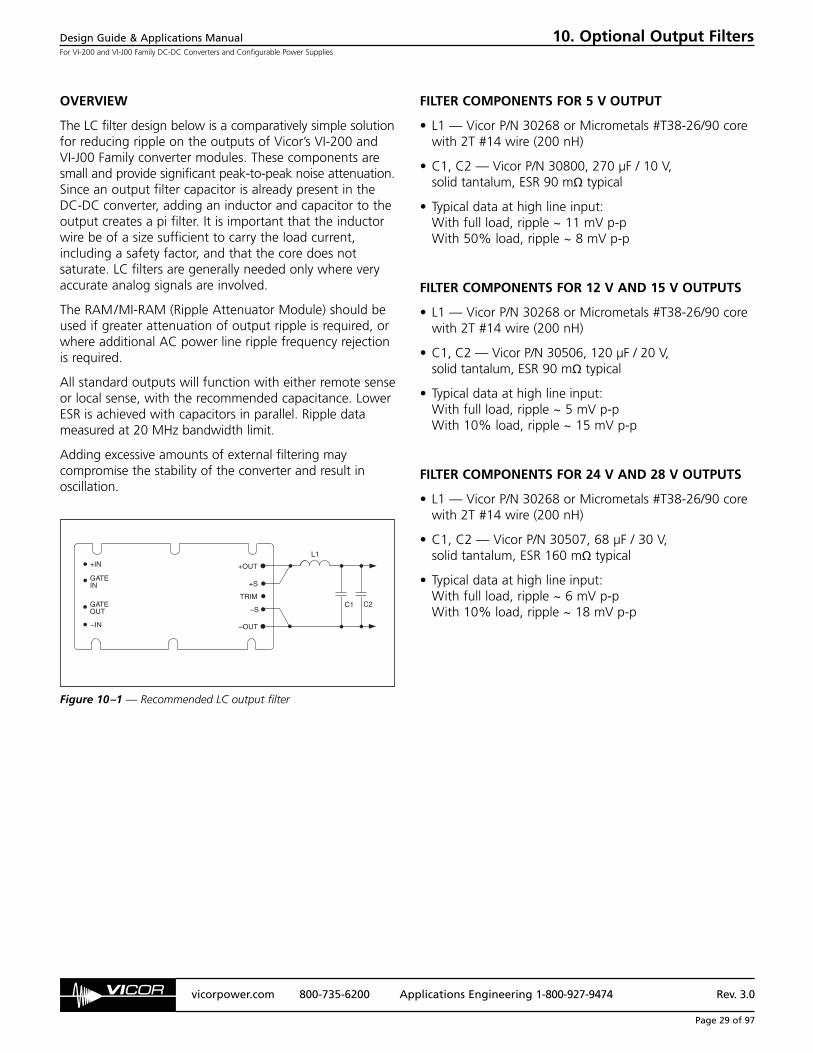
Design Guide & Applications ManualFor VI-200 and VI-J00 Family DC-DC Converters and Configurable Power Supplies
vicorpower.com 800-735-6200 Applications Engineering 1-800-927-9474 Rev. 3.0
Page 29 of 97
OVERVIEW
The LC filter design below is a comparatively simple solutionfor reducing ripple on the outputs of Vicor’s VI-200 andVI-J00 Family converter modules. These components aresmall and provide significant peak-to-peak noise attenuation.Since an output filter capacitor is already present in theDC-DC converter, adding an inductor and capacitor to theoutput creates a pi filter. It is important that the inductorwire be of a size sufficient to carry the load current,including a safety factor, and that the core does notsaturate. LC filters are generally needed only where veryaccurate analog signals are involved.
The RAM/MI-RAM (Ripple Attenuator Module) should beused if greater attenuation of output ripple is required, orwhere additional AC power line ripple frequency rejectionis required.
All standard outputs will function with either remote senseor local sense, with the recommended capacitance. LowerESR is achieved with capacitors in parallel. Ripple datameasured at 20 MHz bandwidth limit.
Adding excessive amounts of external filtering maycompromise the stability of the converter and result inoscillation.
FILTER COMPONENTS FOR 5 V OUTPUT
• L1 — Vicor P/N 30268 or Micrometals #T38-26/90 core with 2T #14 wire (200 nH)
• C1, C2 — Vicor P/N 30800, 270 µF / 10 V, solid tantalum, ESR 90 mΩ typical
• Typical data at high line input:With full load, ripple ~ 11 mV p-pWith 50% load, ripple ~ 8 mV p-p
FILTER COMPONENTS FOR 12 V AND 15 V OUTPUTS
• L1 — Vicor P/N 30268 or Micrometals #T38-26/90 core with 2T #14 wire (200 nH)
• C1, C2 — Vicor P/N 30506, 120 µF / 20 V, solid tantalum, ESR 90 mΩ typical
• Typical data at high line input:With full load, ripple ~ 5 mV p-pWith 10% load, ripple ~ 15 mV p-p
FILTER COMPONENTS FOR 24 V AND 28 V OUTPUTS
• L1 — Vicor P/N 30268 or Micrometals #T38-26/90 core with 2T #14 wire (200 nH)
• C1, C2 — Vicor P/N 30507, 68 µF / 30 V, solid tantalum, ESR 160 mΩ typical
• Typical data at high line input:With full load, ripple ~ 6 mV p-pWith 10% load, ripple ~ 18 mV p-p
–OUT
–S
+S
+OUT+IN
GATEIN
GATEOUT
–IN
TRIM
L1
C1 C2
10. Optional Output Filters
Figure 10–1 — Recommended LC output filter

Design Guide & Applications ManualFor VI-200 and VI-J00 Family DC-DC Converters and Configurable Power Supplies
vicorpower.com 800-735-6200 Applications Engineering 1-800-927-9474 Rev. 3.0
Page 30 of 97
OVERVIEW
The BatMod is a programmable current source modulethat is intended for battery charging or simular currentsource applications. It can be controlled externally to meeta wide range of charging parameters: voltage, current,charge rate and charge time.
The BatMod is comparable to the VI-200 voltage sourcemodule but with a variable current limit. It has threeoutput pins that differ from the VI-200 converters:Current Control (ITRIM), Voltage Adjust (VTRIM) and CurrentMonitor (IMON). All of these pins are referenced to the–OUT pin.
Although the BatMod is primarily intended for batterycharge applications it can be used as a programmablecurrent source for resistive loads or CW laser diodes. TheBatMod will not function properly at zero output voltageand current simultaneously. It follows therefore that thecurrent can not be adjusted to zero with a resistive load.Refer to Safe Operating Area Curves on the BatMod datasheet, which can be found at vicorpower.com.
PINOUT DESCRIPTION
Current Control (ITRIM). An input which can receive ananalog control voltage from 1 – 5 V for adjustment of thesourced current from zero to maximum rating of the BatMod.
Voltage Adjust (VTRIM). An input for controlling orsetting the output setpoint, this is similar to the trimfunction on the VI-200. (Section 5) A maximum voltagecan be set by a fixed resistor or adjusted with an externalvoltage source. A source voltage referenced to –OUTadjusted from 1.25 – 2.5 V will program a 50 – 100% ofrated voltage setting.
It is important to note the nominal output voltage foreach BatMod type untrimmed.
12 Vout Part # = 15 V actual
24 Vout Part # = 30 V actual
48 Vout Part # = 60 V actual
Current Monitor (IMON). An output that indicates theamount of current being sourced. It is a linear voltage /current relationship where one volt corresponds to 0% of sourced current and 5 V corresponds to 100% ofsourced current.
For DC input / current source applications (Figure 11–1), the BatMod has a similar wide range input rating as theVI-200 Family of voltage converters for 48 and 300 Vinputs. BatMods can be used for higher current sourceapplications with a Driver / Booster approach. (Figure 11–2)
NOTE: Inductance to the load should be limited to 20 µH to avoid possible loop instabilities.
2.5 Vdc Max. Vout
=
1.25 Vdc 50% of Vout
5 Vdc 100% of Rating
=
1 Vdc 0 Amps
5 Vdc 100% of Rating
=
1 Vdc 0 Amps
DC Input BatMod
GATEINGATEOUT
+OUT
–OUT
+IN
–IN
ExternalControl Functions
+
–
Load
TRIMVTRIMIMONI
Figure 11–1 — DC input single module
DC Input BatMod
GATEINGATEOUT
+OUT
–OUT
VIMON
+IN
–IN
ExternalControlFunctions
GATEINGATEOUT
+OUT
–OUT
+IN
–IN
BatModBooster
GATEINGATEOUT
+OUT
–OUT
+IN
–IN
Enable/Disable
+
–
LoadTRIM
TRIM
I
BatModBooster
Figure 11–2 — DC input high power array
11. Battery Charger (BatMod)

Design Guide & Applications ManualFor VI-200 and VI-J00 Family DC-DC Converters and Configurable Power Supplies
vicorpower.com 800-735-6200 Applications Engineering 1-800-927-9474 Rev. 3.0
Page 31 of 97
DESIGNING A BATTERY CHARGER
Vicor’s BatMod (current source module) enables designersto easily build a compact, lightweight battery chargingsystem with commonly available parts. The BatModprovides programmable output current and output voltagecapability. Since the BatMod allows the output voltageand the charge current to be set independently, thesystem design is greatly simplified.
Basic Battery Charger. Figure 11–3, shows a basiccharging circuit with a BatMod for the following system requirements:
Battery voltage: 12 VFloat voltage: 13.8 VCharge current: Adjustable 0 – 14.5 A
Setting the Float Voltage. Since the open circuit outputof a 12 V BatMod (VI-2x1-CU-BM) is 15 V, a trim resistor(R3) is necessary to set the float voltage of 13.8 V.
Steps to determine the value of R3:
Solve for VTRIM:
( VFLOAT ) VREF = VTRIMVNOM
(13.8 V) 2.5 V = 2.3 V15 V
Solve for VR5:
VREF – VTRIM = VR5
2.5 V – 2.3 V = 0.2 V
Solve for IR5:
IR5 = VR5 = 0.2 V = 20 µAR5 10 kΩ
Solve for R3:
VTRIM= R3
IR5
2.3 V= 115 kΩ20 µA
A 13.8 V output requires a 115 kΩ resistor.
Setting the Charge Current. The charge current can be programmed from 0 to maximum (14.5 A) by applying1 – 5 V to the ITRIM pin. To determine the voltage requiredto produce a particular charge current, 10 A for example,use the following formula:
4 ( Desired Charge Current ) + 1 = ITRIM voltageMaximum Output Current
4 ( 10 A ) + 1 = 3.76 V14.5 A
To set the input voltage at ITRIM to 3.76 V, adjust thepotentiometer (R2) appropriately.
In Figure 11–3 the configuration will charge the battery at a maximum of 10 A with a 13.8 V float voltage. Othercharge rates and float voltages may be similarly calculated.If a fixed charge current is desired, the potentiometer canbe replaced with two fixed resistors. In applications requiringtight control over the charging current, D1 can be replacedwith a precision reference.
Advanced Battery Charger. Many new battery technologiesrequire sophisticated charging and monitoring systems topreserve their high performance and to extend their life.The Bat Mod serves as an ideal building block forconstructing an advanced battery management system,which typically incorporates a microprocessor-basedcontrol circuit that is easily adapted for a variety of batterychemis tries and monitoring functions. (Figure 11–4)
To maintain the optimum charge on the battery, thecontrol circuit independently adjusts the float voltage andcharge current in response to conditions during thecharge: the battery’s voltage, current, temperature andpressure, and other pertinent parameters. It can also relaybattery status information such as capacity, charge anddischarge history, and cause of failure.
NOTE: A redundant control or monitoring circuitmust be included if failure of the BatMod or itscontrol circuit will result in uncontrolled charging ofthe battery. Many new battery types are sensitive tothese conditions and may result in fire or explosion.
With its wide range of outputs, the BatMod offersdesigners a simple, cost-effective solution to batterycharging for all major battery types.
11. Battery Charger (BatMod)

Design Guide & Applications ManualFor VI-200 and VI-J00 Family DC-DC Converters and Configurable Power Supplies
vicorpower.com 800-735-6200 Applications Engineering 1-800-927-9474 Rev. 3.0
Page 32 of 97
VTRIM
ITRIM
IMON
+OUT
–OUT
To Front End:AIM,HAM,
IAM, orOff-Line
Front End
+IN
–IN
GATEIN
GATEOUT
BatMod VI-2x1-CU-BM
ErrorAmp
R510 kΩ
REF2.5 V
RITRIM
≈ 50 kΩ
10 mA R1820 Ω
D15.1 VZener1 mA
R25 kΩR3
115 kΩ
12 V
Figure 11–3 — Basic charging circuit using a current source module (BatMod)
VTRIM
ITRIM
IMON
Control Circuitry• Voltage• Battery Temp.• Ambient Temp.• Other
+OUT
–OUTSystemStatus
Figure 11–4 — The BatMod in an advanced battery charging system
11. Battery Charger (BatMod)
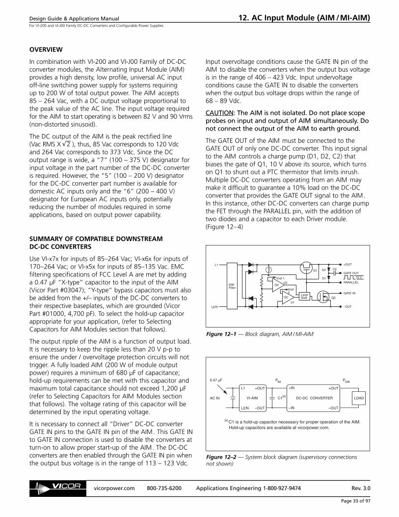
Design Guide & Applications ManualFor VI-200 and VI-J00 Family DC-DC Converters and Configurable Power Supplies
vicorpower.com 800-735-6200 Applications Engineering 1-800-927-9474 Rev. 3.0
Page 33 of 97
OVERVIEW
In combination with VI-200 and VI-J00 Family of DC-DCconverter modules, the Alternating Input Module (AIM)provides a high density, low profile, universal AC inputoff-line switching power supply for systems requiring up to 200 W of total output power. The AIM accepts 85 – 264 Vac, with a DC output voltage proportional tothe peak value of the AC line. The input voltage requiredfor the AIM to start operating is between 82 V and 90 Vrms(non-distorted sinusoid).
The DC output of the AIM is the peak rectified line (Vac RMS X 2 ), thus, 85 Vac corresponds to 120 Vdcand 264 Vac corresponds to 373 Vdc. Since the DCoutput range is wide, a “7” (100 – 375 V) designator forinput voltage in the part number of the DC-DC converteris required. However, the “5” (100 – 200 V) designatorfor the DC-DC converter part number is available fordomestic AC inputs only and the “6” (200 – 400 V)designator for European AC inputs only, potentiallyreducing the number of modules required in someapplications, based on output power capability.
SUMMARY OF COMPATIBLE DOWNSTREAM DC-DC CONVERTERS
Use VI-x7x for inputs of 85–264 Vac; VI-x6x for inputs of170–264 Vac; or VI-x5x for inputs of 85–135 Vac. EMCfiltering specifications of FCC Level A are met by adding a 0.47 µF “X-type” capacitor to the input of the AIM(Vicor Part #03047); “Y-type” bypass capacitors must alsobe added from the +/– inputs of the DC-DC converters totheir respective baseplates, which are grounded (Vicor Part #01000, 4,700 pF). To select the hold-up capacitorappropriate for your application, (refer to SelectingCapacitors for AIM Modules section that follows).
The output ripple of the AIM is a function of output load.It is necessary to keep the ripple less than 20 V p-p toensure the under / overvoltage protection circuits will nottrigger. A fully loaded AIM (200 W of module outputpower) requires a minimum of 680 µF of capacitance;hold-up requirements can be met with this capacitor andmaximum total capacitance should not exceed 1,200 µF(refer to Selecting Capacitors for AIM Modules sectionthat follows). The voltage rating of this capacitor will bedetermined by the input operating voltage.
It is necessary to connect all “Driver” DC-DC converterGATE IN pins to the GATE IN pin of the AIM. This GATE INto GATE IN connection is used to disable the converters atturn-on to allow proper start-up of the AIM. The DC-DCconverters are then enabled through the GATE IN pin whenthe output bus voltage is in the range of 113 – 123 Vdc.
Input overvoltage conditions cause the GATE IN pin of theAIM to disable the converters when the output bus voltageis in the range of 406 – 423 Vdc. Input undervoltageconditions cause the GATE IN to disable the converterswhen the output bus voltage drops within the range of 68 – 89 Vdc.
CAUTION: The AIM is not isolated. Do not place scopeprobes on input and output of AIM simultaneously. Donot connect the output of the AIM to earth ground.
The GATE OUT of the AIM must be connected to theGATE OUT of only one DC-DC converter. This input signalto the AIM controls a charge pump (D1, D2, C2) thatbiases the gate of Q1, 10 V above its source, which turnson Q1 to shunt out a PTC thermistor that limits inrush.Multiple DC-DC converters operating from an AIM maymake it difficult to guarantee a 10% load on the DC-DCconverter that provides the GATE OUT signal to the AIM.In this instance, other DC-DC converters can charge pumpthe FET through the PARALLEL pin, with the addition oftwo diodes and a capacitor to each Driver module. (Figure 12–4)
EMI Filter
10 V
U2
U1
OC
OV
Vref 2
Vref 1
+OUT
–OUT
GATE IN
GATE OUT
PARALLEL
Q1
Q2LevelShift
D2
D1
C2L1
L2/N
Figure 12–1 — Block diagram, AIM / MI-AIM
L1
L2/N
+IN
–IN
+OUT
–OUT
+OUT
–OUT
VI-AIM DC-DC CONVERTERC1[a]
AC IN LOAD
PIM POM0.47 µF
[a] C1 is a hold-up capacitor necessary for proper operation of the AIM. Hold-up capacitors are available at vicorpower.com.
Figure 12–2 — System block diagram (supervisory connections not shown)
√
12. AC Input Module (AIM /MI-AIM)

Design Guide & Applications ManualFor VI-200 and VI-J00 Family DC-DC Converters and Configurable Power Supplies
vicorpower.com 800-735-6200 Applications Engineering 1-800-927-9474 Rev. 3.0
Page 34 of 97
SELECTING CAPACITORS FOR AIM MODULES
Hold-up Time. For maximum flexibility, an externalcapacitor (Figure 12–2, C1) is used to set the system’shold-up requirements. Hold-up time, for purposes of thisapplication note, is defined as the time interval from lossof AC power to the time a DC-DC converter begins todrop out of regulation (Figure 12–3, T4 to T5). Hold-uptime is a function of line voltage, hold-up capacitance,output load, and that point on the AC waveform wherethe line drops out. For example, if the AC line fails justafter the hold-up capacitors were recharged, hold-up timewill be much greater (Figure 12–3, T3 to T5) than if theAC line fails just prior to another recharge (Figure 12–3,T4 to T5).
The basic equations involved in calculating hold-up time are:
1 X C1 X Vp2 – 1 X C1 X Vdo2 = PIM X (T5 – T3) (1)2 2
solving for C1:
C1 = 2 XPIM x (T5 – T3)
(2)Vp2 – Vdo2
Where PIM is power delivered from the AIM:
PIM = Module Output Power = POM (3)Module Efficiency Eff. % / 100
The energy (Joules) delivered from the AIM from the timepower is lost (T4), until loss of an output (Figure 12–2, T5):
Energy (Joules) = PIM x (T5 - T4) (Watt – Seconds) (4)
where: POM = Output power from all the modules
PIM = Input power to the modules(output power from the AIM)
Eff = Weighted average efficiency of all modules
The input power to the converter(s) during normal operationis supplied from the AC line during the conduction timeof the rectifiers (T2 to T3) internal to the AIM and by theenergy stored in C1 when the rectifiers in the AIM arereverse biased (T1 to T2). In the event of an AC failure(T4), C1 must continue to provide energy to the convertersuntil either AC returns or the converter drops out (T5).
The energy stored in C1 at the peak of the AC is:
1x C1 x Vp2 = Joules (5)
2
The energy stored in C1 when the converter drops out ofregulation is:
1 x C1 x Vdo2 = Joules (6)2
The energy delivered by C1 to the converters duringnormal operation is:
PIM x (T2 – T1) = Joules (7)
RECTIFIEDAC
T0 T1 T2 T3 T4
Vp
Vv
Vdo
TIME
T5
Figure 12–3 — AC waveforms
12. AC Input Module (AIM /MI-AIM)

Design Guide & Applications ManualFor VI-200 and VI-J00 Family DC-DC Converters and Configurable Power Supplies
vicorpower.com 800-735-6200 Applications Engineering 1-800-927-9474 Rev. 3.0
Page 35 of 97
CHOOSING APPROPRIATE VALUES FOR AIM MODULES
Sample calculation:
Converter output power (POM) = 100 W
Line frequency = 60 Hz
Line range = 105 – 264 Vac
Efficiency = 82%
Desired hold-up time = 5 ms (minimum)
therefore:
PIM = 100 = 122 W0.82
T5 – T3 = 5 ms + 8.3 ms = 13.3 ms(minimum hold-up time plus half cycle)
Vp = 105 X 2 = 148 V
Vdo = 100 V
and:
C1 =2 X 122 X 0.0133
1482 – 1002
C1 = 270 µF
where:
VP = The peak of the rectified AC line or 2 X Vac in. For an input range of 85 – 264 Vac, this voltage will vary from 120 – 373 V.
VV = The low point of the rectified AC line under normal operating conditions. This “valley” voltage is a function of C1, PIM and line frequency. The peak-to-peak ripple across C1 is VP – VV and determines the ripple current in C1.
NOTE: It is important to verify the rms ripple current in C1 with a current probe.
Vdo = Voltage at which the DC-DC converter(s) begin(s) to drop out of regulation. This voltage is from the data sheet of the appropriate module, which for the VI-270 Family is 100 Vdc. Under normal operating conditions, VV must exceed Vdo.
T1 = The peak of the rectified AC line or the point at which C1 is fully charged. For an input range of 85 – 264 Vac, this voltage will vary from 120 – 373 V.
T2 = The low point of the rectified AC line under normal operating conditions and the point at which C1 is about to be “recharged”. This is the point of lowest energy in C1.
T4 = The low point of the rectified AC line; the point of lowest energy in C1; the point at which if the AC line fails, hold-up time is shortest, i.e., “worst case”.
T5 = The time at which the converter(s) drop out of regulation.
T5 – T4 = Minimum hold-up time. Actual hold-up time may vary up to a maximum of T5 – T3.
(T3 – T1) X 2 = One line cycle.
The following values are calculated in a similar manner.
C1 values as a function of line voltage, frequency anddelivered power, for use with the “7” input designatorDC-DC converters (AIM input of 90–264 Vac) or “5” inputdesignator (AIM input of 90–132 Vac) DC-DC converters.
NOTE: With “7” input DC-DC converters operatedfrom the AIM input range of 90 – 264 Vac, 400 Vcapacitors must be used (Vicor Part #30240). With“5” input DC-DC converters used over the AIM inputrange of 90 – 132 Vac, 200 V capacitors may be used(Vicor Part #30769).
C1 values as a function of line voltage, frequency anddelivered power, for use with the “6” input designatorDC-DC converters (AIM input of 180 – 264 Vac).
NOTE: With “6” input DC-DC converters operatedfrom the AIM input range of 180 – 264 Vac, 400 V capacitors must be used (Vicor Part #30240).
√
√
50 W 270 µF 135 µF 300 µF 150 µF75 W 400 µF 200 µF 440 µF 230 µF100 W 525 µF 270 µF 600 µF 300 µF150 W 800 µF 400 µF 890 µF 455 µF200 W 1,000 µF 540 µF 1,180 µF 600 µF
Table 12–1 — Hold-up capacitor values for use with VI-270/VI-J70and the VI-250/VI-J50 DC-DC converters.
Module(s) 60 Hz 50 HzDelivered Power 90 Vac 105 Vac 90 Vac 105 Vac
Table 12–1 — Hold-up capacitor values for use with VI-260/VI-J60DC-DC converters.
12. AC Input Module (AIM /MI-AIM)
50 W 66 µF 34 µF 74 µF 38 µF75 W 100 µF 50 µF 110 µF 60 µF100 W 130 µF 67 µF 150 µF 75 µF150 W 200 µF 100 µF 220 µF 115 µF200 W 262 µF 135 µF 300 µF 150 µF
Module(s) 60 Hz 50 HzDelivered Power 180 Vac 210 Vac 180 Vac 210 Vac

Design Guide & Applications ManualFor VI-200 and VI-J00 Family DC-DC Converters and Configurable Power Supplies
vicorpower.com 800-735-6200 Applications Engineering 1-800-927-9474 Rev. 3.0
Page 36 of 97
D1D2
D2
C2
C2
–OUT
–STRIM
+S
+OUT+INGATEINGATEOUT–IN
–OUT
–STRIM
+S
+OUT+INGATEINGATEOUT–IN
–OUT
–STRIM
+S
+OUT+INGATEINGATEOUT–IN
AIM
GATE OUTPAR
GATE IN
+OUT
–OUTL2/N
NC
NC
L1
D1, D2: 1N4148C2: 470 pf / 500 VD3: 1N4006
D1
UniversalAC In
Bussman Fuses,PC Tron
0.47 μF
C1[a]
Driver
Driver
Driver
[a] Refer to Selecting Capacitors for AIM Modules in the begining of this Section. Refer to Typical application for Vicor converter with AIM, Figure 12–5, for recommended external components.
D3
D3
D3
Y-capacitors not shown for clarity
UniversalAC In
AIM
GATE OUTPAR
GATE IN
+OUT
–OUTL2/N
NC
NC
L1
0.47 µF
–OUT
–STRIM
+S +OUT+IN
GATEINGATEOUT–IN
VI-200/J00Driver
Load
F2
0.01 µF (Two 4,700 pF)Y-Rated Capacitors
0.01 µF (Two 4,700 pF)Y-Rated Capacitors
0.01 µF Ceramic
0.01 µF Ceramic
C1[a]
F1
[a] Consult factory or refer to Selecting Capacitors for AIM Modules at the begining of this section.
Z1: MOV Part #30076
Fuse 1: 6.3A/250V (IEC 5X20 mm) Buss GDB-6.3 or 7 A / 250 V (3AG 1/4" x 1 1/4") Littlefuse 314-007
Fuse 2: For VI-X7X-XX — Buss PC-Tron 2.5 A (250 V) For VI-X6X-XX — Buss PC-Tron 3 A (250 V) For VI-X5X-XX — Buss PC-Tron 5 A
Z1
Figure 12–4 — AIM connection diagram, multiple Driver DC-DC converters
Figure 12–5 — Typical application for Vicor converter with AIM
12. AC Input Module (AIM /MI-AIM)

Design Guide & Applications ManualFor VI-200 and VI-J00 Family DC-DC Converters and Configurable Power Supplies
vicorpower.com 800-735-6200 Applications Engineering 1-800-927-9474 Rev. 3.0
Page 37 of 97
13. AC Input Harmonic Attenuator Module (HAM)
THE HARMONIC ATTENUATOR MODULE COMPATIBLE WITH VI-26x AND VI-J6x FAMILIES
The Harmonic Attenuation Module (HAM) consists of afull-wave rectifier, a high-frequency zero-current-switching(ZCS) boost converter, active inrush current limiting, short-circuit protection, control, and housekeeping circuitry(Figure 13–1). The incoming AC line is rectified and fed tothe boost converter. The control circuitry varies theoperating frequency of the boost converter to regulateand maintain the output voltage of the HAM above thepeak of the incoming line, while forcing the input currentto follow the waveshape and phase of the line voltage. Apower factor better than 0.99 is achieved (Figure 13–2).Operating efficiency of the boost converter is optimized at any incoming line voltage by an adaptive outputvoltage control scheme.
The output voltage of the HAM varies as a function ofincoming AC line voltage (Figure 13-3). On a nominal 120Vac line the output voltage of the HAM is 260 Vdc — wellwithin the input operating voltage range of Vicor VI-26xand VI-J6x converters. As input line increases, so does theHAM output voltage; at 220 Vac the delivered voltage willbe about 350 V. For any given input line voltage, the HAMmaintains enough headroom between the output voltageand peak input voltage to ensure high quality activepower factor correction without unnecessarily sacrificingoperating efficiency.
The HAMD version does not contain an internal bridgerectifier and is intended for configuring higher power arrayswith Booster versions, referred to as the VI-BAMD(Figure 13–5).
L1 and L2/N (HAM) Pin. An appropriate line filter isrequired to limit conducted emissions and ensure reliableoperation of the HAM, see page 40. Connect single phaseAC mains to the input of the line filter via a 10 A, 250 Vfuse. Connect the output of the filter to L1 and L2/N ofthe HAM. Do not put an X-capacitor across the input ofthe HAM or use a line filter with an X-capacitor on itsoutput as power factor correction may be impacted.
+IN, –IN (HAMD, BAMD) Pin. These pins are connectedto the output of the external bridge rectifier in HAMD /BAMD configurations (Figure 13–5).
GATE IN (HAM) Pin. The user should not make anyconnection to this pin.
GATE IN (HAMD) Pin. This pin provides line voltageenvelope and phase information for power factorcorrection. This connection must be made through thesynchronization diodes between the line filter and bridgerectifier (Figure 13–5).
Note:Non-Isolated Output
Gate InGate Out
ZCSBoost
Converter
Inrush& ShortCircuit
Protection
High FrequencyControl
VoltageWaveform
CurrentSense
ACLine
Control& House-keepingCircuitry
Output VoltageModule Enable
Power OK
DCOut
Recti-fier
Aux. Supply
+
–
NOTE: No input to output isolation.
Figure 13–1 — HAM block diagram (HAMD version has the rectifier block deleted.)
Input VoltageVRMS
Rated Output Power
Output Voltage
Out
put P
ower
(W)
Out
put V
olta
ge (V
dc)
350
400
450
500
550
600
650
85190
260
330
400
365
435
295
225
95 105 115 125 135 145 155 165 175 185 195 205 215 225 235 245 255 265
110 Vac
700
derate output power 8 W/V for Vin <110 Vac
Figure 13–3 — Output voltage and power rating vs. input voltage
Figure 13–2 — Input voltage and current wave forms, without andwith power factor correction.
Design Guide & Applications ManualFor VI-200 and VI-J00 Family DC-DC Converters and Configurable Power Supplies
vicorpower.com 800-735-6200 Applications Engineering 1-800-927-9474 Rev. 3.0
Page 38 of 97
13. AC Input Harmonic Attenuator Module (HAM)
GATE IN (BAMD) Pin. The Gate In pin is an interface pinto the Gate Out pin of a HAMD or BAMD depending onconfiguration. The user should not make any otherconnection to this pin.
GATE OUT Pin. The Gate Out pin is a synchronization pinfor HAMD/BAMD arrays; the user should not make anyother connection to this pin.
+OUT and -OUT Pin. Connect the +OUT of the HAM tothe +IN of the respective Vicor DC-DC converters with therecommended fuse. Connect the -OUT of the HAM to the-IN of the converters. In addition, an external hold-upcapacitor of 1,000 µF with a minimum voltage rating of450 Vdc, is required (across the output of the HAM) for16 ms ride through time at full power (500 µF for halfpower, etc). This capacitor must be in close proximity tothe HAM. Do not exceed 3,000 µF of total outputcapacitance. Lower values of capacitance may be used forreduced hold up requirements, but not less than 500 µF.Lower capacitance values may degrade power factorspecifications.
Auxiliary Supply (A/S) Pin. The HAM provides a lowvoltage non isolated output Auxiliary Supply (A/S) thatmay be used to power primary side control andmonitoring circuitry. This output is 19 – 23 Vdc,referenced to -OUT, at 3 mA max. Do not overload orshort this output as the HAM will fail. A typical use forA/S is to power an optical coupler that isolates the PowerOK signal (Figure 13–6).
Enable Output (E/O) Pin. The Enable Output (E/O) isused to inhibit the DC-DC converters at start up until thehold up capacitors are charged, at which time Enable isasserted high (open state, Figure 13–8). If the AC linefails, E/O goes low when the DC output of the HAMdrops below 195 Vdc.
E/O must be connected to the Gate Input of all VI-26x and VI-J6x drivers (Figure 13–4); failure to do so may cause theconverters to toggle on and off. It is not necessary toconnect this pin to boosters as they are controlled by theirrespective driver. If an external load is connected directlyto the output of the HAM, do not apply the load until theoutput hold up capacitor(s) are fully charged.
The E/O pin ancillary circuitry illustrated in Figures 13–4 and13–5 provides transient immunity. The illustrated circuitry isthe minimum required, see Figures 13–4 and 13–5.
Power OK (P/OK) Pin. Power OK is a monitor signal thatindicates the status of the AC mains and the DC outputvoltage of the HAM. P/OK is asserted (active low) whenthe output bus voltage is within normal operating range20 – 25 ms after DC-DC converters are enabled by the
E/O signal of the HAM. This provides sufficient time forthe converters to turn on and their output(s) to stabilizeprior to P/OK being asserted (Figure 13–9). For momentaryinterruptions of AC power, the HAM will provide at least16 ms of ride through or hold up time (with 1,000 µFoutput capacitor). On loss of power or brownout, (whenthe HAM output voltage drops below 230 Vdc) the P/OKsignal will go to an open circuit state (see Figure 13–7),signaling an impending loss of input power to theconverter modules. P/OK will provide power fail warningat least 1 ms prior to converter shut down. When theHAM output voltage drops below 195 Vdc the convertersare disabled via Enable Output (E/O).
SAFETY NOTES
Each HAM, HAMD or BAMD module must bepreceded by a safety agency recognized fast-blow10A 3AG fuse.
The HAM is not isolated from the line – either inputor output; a line isolation transformer must be usedwhen making scope measurements. HAMs do notprovide input to output isolation. Differential probesshould be used when probing the input and outputsimultaneously to avoid destructive ground loops.
PROTECTIVE FEATURES
Over Temperature Shut Down. The HAM is designed toshut down when the temperature of the baseplateexceeds 90°C. Do not operate the HAM above itsmaximum operating temperature of 85°C.
Short Circuit Protection. The HAM contains output shortcircuit protection. Operation of this function does notclear the input fuse and the output will resume normaloperation after removal of the fault. A short period of time may be required to allow forcooling of an internal temperature sensor.
Output Over Voltage Protection. The HAM containsoutput over voltage protection. In the event the outputvoltage exceeds approximately 420 Vdc, the boost willdecrease to maintain 420 Vdc on the output. When thepeak of the AC line exceeds 420 V (approximately 293 Vac) the boost will have been reduced to zero andthe E/O line will be pulled low shutting down the converters. Beyond this the protection circuit will beenabled and the output voltage will decrease.
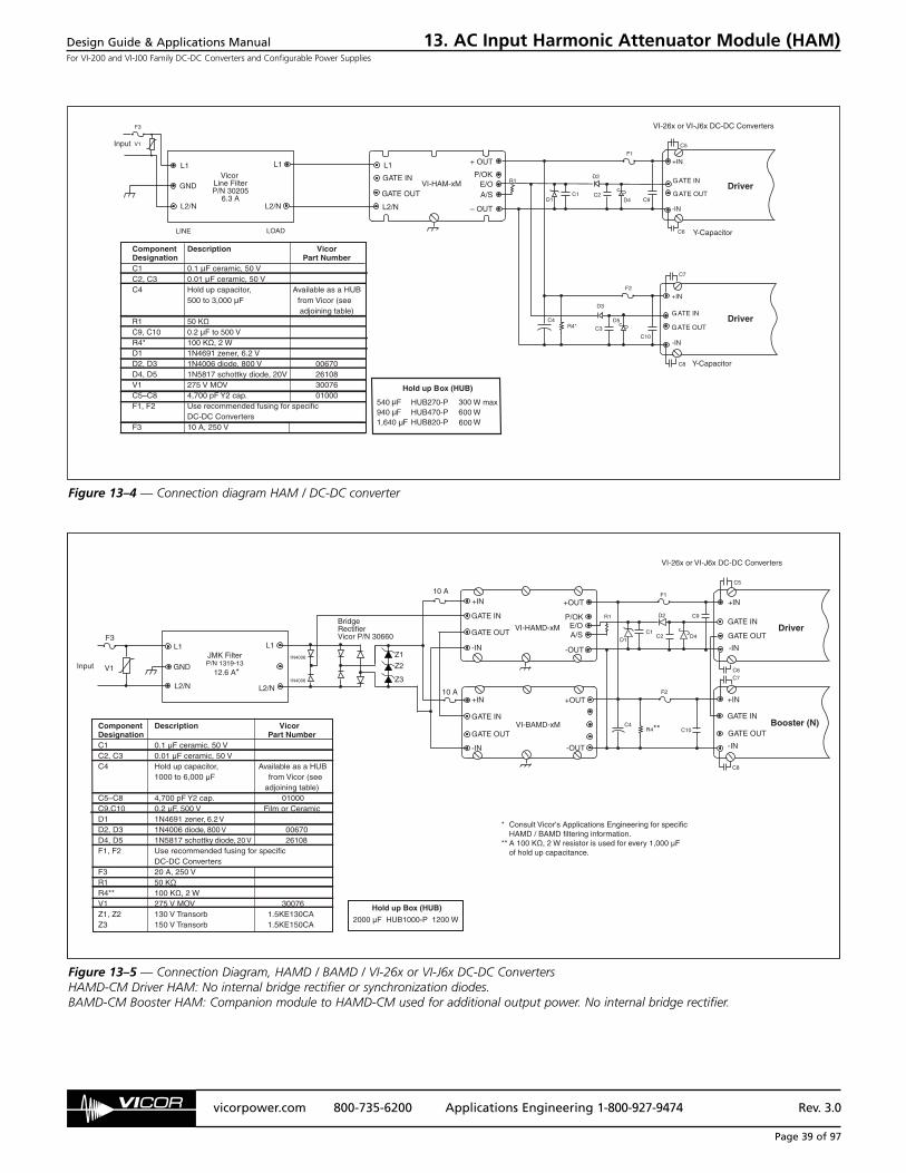
Design Guide & Applications ManualFor VI-200 and VI-J00 Family DC-DC Converters and Configurable Power Supplies
vicorpower.com 800-735-6200 Applications Engineering 1-800-927-9474 Rev. 3.0
Page 39 of 97
13. AC Input Harmonic Attenuator Module (HAM)
Figure 13–5 — Connection Diagram, HAMD / BAMD / VI-26x or VI-J6x DC-DC ConvertersHAMD-CM Driver HAM: No internal bridge rectifier or synchronization diodes.BAMD-CM Booster HAM: Companion module to HAMD-CM used for additional output power. No internal bridge rectifier.
Component Description VicorDesignation Part NumberC1 0.1 μF ceramic, 50 VC2, C3 0.01 μF ceramic, 50 VC4 Hold up capacitor, Available as a HUB 1000 to 6,000 μF from Vicor (see adjoining table)C5–C8 4,700 pF Y2 cap. 01000C9,C10 0.2 μF, 500 V Film or CeramicD1 1N4691 zener, 6.2 VD2, D3 1N4006 diode, 800 V 00670D4, D5 1N5817 schottky diode, 20 V 26108F1, F2 Use recommended fusing for specific DC-DC ConvertersF3 20 A, 250 VR1 50 KΩ
R4** 100 KΩ, 2 WV1 275 V MOV 30076Z1, Z2 130 V Transorb 1.5KE130CAZ3 150 V Transorb 1.5KE150CA
+IN
VI-26x or VI-J6x DC-DC Converters
GATE IN
GATE OUT
-IN
-IN
F2
+IN
F1
R1
D1
D2
D4C2
C4
C5
C6C7
C8
JMK FilterP/N 1319-13
12.6 A*
+IN
GATE IN
GATE OUT
-IN
+OUT
-OUT
P/OKE/OA/S
VI-HAMD-xM
GATE IN
GATE OUT
-IN
+IN +OUT
-OUT
VI-BAMD-xM
Input
BridgeRectifierVicor P/N 30660
L1
GND
L2/N
L1
L2/N
1N4006
1N4006
F3
R4**
C1
V1
C9
C10
* Consult Vicor's Applications Engineering for specific HAMD / BAMD filtering information.** A 100 KΩ, 2 W resistor is used for every 1,000 μF of hold up capacitance.
Z1
Z2
Z3
10 A
10 A
Hold up Box (HUB)
2000 μF HUB1000-P 1200 W
GATE IN
GATE OUT
Driver
Booster (N)
+IN
-INL2/N
GATE OUT
GATE IN
L1
– OUT
E/O
+ OUT
A/S
P/OKVI-HAM-xM
-IN
Y-Capacitor
Y-Capacitor
F2
+IN
L1
GND
L2/N
L1
LOAD
L2/N
Vicor Line FilterP/N 30205
6.3 A
LINE
F1
GATE IN
GATE OUT
Hold up Box (HUB)
R1
C3
D3
D5
D1 D4C2
C5
C6
C7
C8
C1
R4*C4
D2
F3
Driver
Component Description VicorDesignation Part NumberC1 0.1 µF ceramic, 50 VC2, C3 0.01 µF ceramic, 50 VC4 Hold up capacitor, Available as a HUB 500 to 3,000 µF from Vicor (see adjoining table)R1 50 KΩ
C9, C10 0.2 µF to 500 VR4* 100 KΩ, 2 WD1 1N4691 zener, 6.2 VD2, D3 1N4006 diode, 800 V 00670D4, D5 1N5817 schottky diode, 20V 26108V1 275 V MOV 30076C5–C8 4,700 pF Y2 cap. 01000F1, F2 Use recommended fusing for specific DC-DC ConvertersF3 10 A, 250 V
V1
µµ
µ
Input
C9
C10
VI-26x or VI-J6x DC-DC Converters
GATE IN
GATE OUT
Driver
Figure 13–4 — Connection diagram HAM / DC-DC converter

Design Guide & Applications ManualFor VI-200 and VI-J00 Family DC-DC Converters and Configurable Power Supplies
vicorpower.com 800-735-6200 Applications Engineering 1-800-927-9474 Rev. 3.0
Page 40 of 97
13. AC Input Harmonic Attenuator Module (HAM)
LIN
E
LOA
D
R Cx
LD LC Cy
Cy
D1
D2
D3
HAM Filter P/N 30205
R = 235 KΩ D1,2 = 1.5KE130CA D3 = 1.5KE150CA
MOV*P/N 30076
Cx = 1.5 uF(x2)SH Cy = 0.01 uF, Y2 type LC = 6.9 mH LD = 0.72 mH
*MOV required external to filter to meet normal mode transient surge requirements
Figure 13–10 — Recommended HAM filter
+OUT
P/OK
–OUT
E/O
A/S
18 kΩ, 1/4 W
"Power OK" StatusLow = OK
LOGIC
P/OK
–OUT
+OUT
E/OS
G
D
A/S
Figure 13–6 — Auxiliary Supply (A/S) Figure 13–7 — Power OK (P/OK)
LOGIC
E/O
–OUT
+OUT
P/OK
A/S
SG
D
Figure 13–8 — Enable Output (E/O)
OutputsDC-DC Converter(s)
Rectified Line
Enable Output (E/O)
DC Outputof HAM
Power OK (P/OK)
AC Mains120 Vrms
Boost Voltage
195 Vdc
240 Vdc
Off at 195 Vdc
Off at 230 Vdc
230 Vdc
25 ms
10 ms
Off below 195 Vdc
Figure 13–9 — Start-up / shut-down timing diagram
A/S
E/O
P/OK
+OUT
–OUT
IAS ≤ 3 mA
19 – 23 V+
–
DO NOT OVERLOADor directly connect a capacitorto the A/S terminal.
A line filter is required to provide attenuation ofconducted emissions generated by the HAM module andto protect it from line transients. It also presents a welldefined high frequency AC line impedance to the input ofthe HAM. To meet the listed specifications, Vicor’s P/N30205 line filter/transient suppressor or equivalent mustbe used (Figure 13–10). The addition of a MOV externalto this filter is required to meet normal mode transientsurge requirements.
For applications using HAMD + BAMD or where the userdesires to construct a custom HAM filter, the filter shouldbe designed following Figure 13–10, the schematic ofVicor’s P/N 30205 filter. The current carrying capability ofthe inductors must be scaled proportionally to the numberof HAM modules used. Inductance values must beselected according to Table 13–1. These limits are toensure proper operation of the HAM and do notguarantee a system will meet conducted emissionsspecifications.
For applications requiring magnetic field shielding, do notplace a ferrous EMI shield over the plastic cover of theHAM module. This can cause thermal problems due toinduction heating effects.
LINE FILTER FOR HIGH BOOST HAM
Parameter Min Typ Max UnitDifferential Mode 0.2 0.35 0.75 mHInductance (LD)
Common Mode 3 6 mHInductance (LC)
Table 13-1 — HAM filter inductance range

Design Guide & Applications ManualFor VI-200 and VI-J00 Family DC-DC Converters and Configurable Power Supplies
vicorpower.com 800-735-6200 Applications Engineering 1-800-927-9474 Rev. 3.0
Page 41 of 97
13. AC Input Harmonic Attenuator Module (HAM)
90
80
70
60
50
40
OP
ER
AT
ING
TE
MP
(D
EG
C)
CURRENT (AMPS)
RATED CURRENT VS AMBIENT TEMPERATURE
1.0 2.0 3.0 4.0 5.0 6.0 7.0
Figure 13–12 — HAM filter’s current rating vs. temperature
90
80
70
60
50
40
30
20
10
0
DM
CM
0.01 0.04 0.1 0.4 1 4 10 40 1000.02 0.07 0.2 0.7 2 7 20 70
FREQUENCY (MEGAHERTZ)
INS
ER
TIO
N L
OS
S (
db)
Figure 13–13 — HAM filter insertion loss vs. frequency
'0'
FACE MAY BEBOWED 0.04 MAX
4-40 INSERT0.25 DP 4 PL
ø0.080 PIN6 PLACES
LOA
D
LIN
E
0.9000.100
1.200
0.500 0.500
4.60 ±0.02
0.060
1.00 MAX
0.13 ±0.02
1.45±0.02
2.800
2.50
2.00
0.30 ±0.02
1.800
PL
PL
PL
2.40±0.02
Figure 13–11 — HAM filter mechanical diagram
Table 13-2 — HAM filter part #30205 specifications
Parameter Min Typ Max UnitOperating voltage 85 250 Vac
Operating temperature (See Fig.13-12) –20 50 °C
Leakage current at 264 Vac, 63 Hz 1.2 mA(Either line to earth)
Operating current 6.3 A
Dielectric withstand (line – case) 1500 Vac
Residual voltage after 1 sec. 34 V
Operating frequency 50 60 Hz
Agency Approvals UL, CSA, TÜV

Design Guide & Applications ManualFor VI-200 and VI-J00 Family DC-DC Converters and Configurable Power Supplies
vicorpower.com 800-735-6200 Applications Engineering 1-800-927-9474 Rev. 3.0
Page 42 of 97
13. AC Input Harmonic Attenuator Module (HAM)
HAM DO’S AND DON’TS
The following cautions should be observed before applyingpower to the HAM.
• It is important that the output of the HAM not be loaded until the input voltage has exceeded 85 Vac and the output has begun to boost to 260 Vdc. This means that if the load on the HAM is a Vicor converter, the ENABLE Output of the HAM must be connected to the GATE IN of all Driver modules. The HAM will then disablethe module output until the input exceeds 85 Vac and the output has been boosted to 260 Vdc. If an external load is connected directly to the output of the HAM, donot apply the load until the output of the HAM is stabilized in boost mode.
• Although the efficiency of the HAM is quite high, it still dissipates significantly more power than a VI-26x DC-DC converter. Care should be taken to cool it. Do not rely on the internal overtemperature shut down to take the place of adequate planning relative to the cooling of the HAM. Thermal compound should be used between the heat sink and baseplate of the HAM, HAMD and BAMD.
• Power factor is 0.997 at 120 Vac and 0.995 at 240 Vac. Harmonic content at 240 Vac is therefore somewhat higher than at 120 Vac. Remember that harmonic content measured cannot be any lower than the harmonic content of the AC mains. A precision AC source is required for accurate power factor measurements.
• The input voltage range of the HAM is 85 – 264 Vac; however it may not start boosting until the AC mains has exceeded 87 Vac. Once the HAM has started, it will operate down to 85 Vac. The HAM contains 2.5 – 6 V of input hysteresis, therefore if the AC line impedance ishigh, i.e., when using a variable autotransformer, the HAM may start, but the AC line may then fall enough to drop below undervoltage lockout. When this happens the AC line will go up, the HAM starts and thecycle repeats. Therefore avoid soft AC lines at or near low line.

Design Guide & Applications ManualFor VI-200 and VI-J00 Family DC-DC Converters and Configurable Power Supplies
vicorpower.com 800-735-6200 Applications Engineering 1-800-927-9474 Rev. 3.0
Page 43 of 97
OVERVIEW
The IAM is a component-level, DC input front-end filterthat when used in conjunction with the Vx-200 and Vx-J00 Family of DC-DC converters provides a highlyefficient, high density power system with outputs from 1 – 95 Vdc and power expansion from 25 – 800 W.
There are five input attenuator modules available for thecommercial market that comply with telecommunicationand industrial control EMC specifications: Refer to datasheets for applicable standards at vicorpower.com.
There are two input attenuator modules available for thedefense market that comply with military EMC specifications,transient specifications and spike specifications. Refer toproduct data sheet for applicable standards at vicorpower.com.
EMC
EMC performance is guaranteed when the IAM is used inconjunction with the recommended Vicor converterswithin the permissible power rating and in accordancewith the recommended installation procedure. (Figure14–3)The capacitor shown across the input of the converter andbypass capacitors shown on the –IN and +IN of the DC-DCconverters to ground are required to meet EMC specifications.The capacitors should be Y-rated (interference suppression).Y capacitors have high voltage breakdown ratings to meetthe isolation characteristics of the module’s input tobaseplate specification, self-healing properties, and safetyagency approvals.
INPUT REVERSE POLARITY PROTECTION
A Zener diode in the EMC filter provides reverse polarityprotection when used with a properly rated fuse externalto the IAM. The characteristics of the recommended inputline fuses permit normal full load operation withprotection in the event of a reverse polarity by clearing ofthe fuse. (Table 4–3).
INPUT TRANSIENT PROTECTION
A Zener diode, inductor and capacitor in the EMC filterprotect against short term transients. Transient voltagesthat persist beyond these limits are dropped across an N-channel enhancement FET, Q1. It is necessary that theFET be kept in saturation mode during normal operation.Thus it is necessary to connect the DC-DC converters’GATE OUT to the IAM’s GATE OUT to charge pump the
10VU2
U1OC
OVVref
2
Vref 1
+OUT
–OUT
LevelShift–IN
+IN
–IN
+IN
GATE IN
GATE OUT
PARALLEL
Q1
Q2
EMI Filter
D1
D2
C2
14. Input Attenuator Module (IAM/ MI-IAM)
VI-A11-xU 24 V (21 – 32 V) 200 WVI-AWW-xU 24 V “W” (18 – 36 V) 200 WVI-A33-xQ 48 V (42 – 60 V) 400 WVI-ANN-xQ 48 V “N” (36 – 76 V) 400 WVI-A66-xQ 300 V (200 – 400 V) 400 W
[a] Based on DC-DC converters with 5 V outputs or higher.
Table 14–1 — Output power capability
Table 14–2 — Output power capability
Figure 14–1 — Block diagram of Input Attenuator Module (IAM)
Input Maximum Output Power[a]Model Voltage Range of Converter Combinations
MI-A22-xU 28 V (16 – 50 V) 200 WMI-A66-xU 270 V (125 – 400 V) 200 W
Input Maximum Output PowerModel Voltage Range of Converter Combinations

Design Guide & Applications ManualFor VI-200 and VI-J00 Family DC-DC Converters and Configurable Power Supplies
vicorpower.com 800-735-6200 Applications Engineering 1-800-927-9474 Rev. 3.0
Page 44 of 97
gate of the FET to a voltage in excess of its source. In thecase where multiple DC-DC Driver modules are connectedto one IAM, an external charge pump through the PARALLELpin (connected to the gate of the FET) must be added toensure that the FET remains enhanced in the event GATEOUT enhancement is lost (Figure 14–4). The additionalcircuitry, C2, D1 and D2 are added externally to chargepump through the PARALLEL pin.
Shut down of the DC-DC converters is accomplished bysaturating Q2 during an input overvoltage to preventpossible damage to the converters. The IAM will automaticallyrestart when the input overvoltage is reduced to withinthe input voltage range.
If the long term transient withstand specifications areexceeded, the recommended external fuse will clear.
INPUT CURRENT
Inrush current is a function of the number of DC-DCconverters that are connected to the input attenuatormodule (modules are not gated off at turn-on) and theamount of external capacitance added between the InputAttenuator Module and the DC-DC converter. The inrushcurrent specification is 125% of steady state input currentfor 10 ms. To avoid excessive dissipation in the elementcontrolling the inrush (Q1), the following maximum valuesof external capacitance must be adhered to.
14. Input Attenuator Module (IAM/ MI-IAM)
0.1 1 10ms 100 1000
100V
Normal Operating Area
I.S.W.Full Load
100V
Standard Wide Range24 V Inputs
0.1 1 10ms 100 1000
800V
Normal Operating Area
I.S.W.Full Load
300 V Input
S.D.
160V
0.1 1 10ms 100 1000
Normal Operating Area
I.S.W.Full Load
48 V Input
R.E.
276V
Normal Operating Area
I.S.W.Full Load
0.1 1 10ms 100 1000
48 V Wide Range Input
R.E.
S.D.
R.E.R.E.
32V
21V
36V
18V
S.D.
76V
125V
60V
100V
42V
500V
400V
200V36VS.D.
S.D. 100V
500ms 500ms
I.S.W.: Input surge withstand (no disruption of performance)R.E.: Ratings exceededS.D.: Shut down
VO
LTS
-PE
AK
VA
LUE
OF
SP
IKE
VO
LTA
GE
TIME (SECONDS)
1s010
100ms-110
10ms-210
1ms-310-410-510-610
-600
-500
-400
-300
-200
-100
0
100
200
300
400
500
600
Ratings Exceeded
Reverse Polarity
50VOVP
VO
LTS
-PE
AK
VA
LUE
OF
SP
IKE
VO
LTA
GE
TIME (SECONDS)
1s010
100ms-110
10ms-210
1ms-310-410-510-610
600
400
200
0
200
400
600
800Ratings Exceeded
Reverse Polarity
500OVP 400
28 Vdc Input
270 Vdc Input
Safe Operating Area(1% duty cycle max., Zs = 0.5Ω, for short duration transient capability refer to specifications)
Figure 14–2 — Safe operating area based on input voltage of IAM
24 V 20 A / 32 V (AGC-20)24 V “W” 20 A / 36 V (AGC-20)48 V 20 A / 60 V (3AB-20)48 V “N” 20 A / 80 V (3AB-20)300 V 5 A / 250 V Bussman PC-Tron28 V 20 A / 250 V (3AB-20 or F03A, 125 V, 20 A)270 V 5 A / 250 V Bussman PC-Tron or F03A, 250 V, 4 A
Table 14–3 — Recommended fusing based on input voltage
Input Voltage Recommended Fuse
24 Vdc (21 – 32 V) 470 µF24 Vdc (18 – 36 V) 470 µF28 Vdc (18 – 50 V) 390 µF48 Vdc (42 – 60 V) 220 µF48 Vdc (36 – 76 V) 120 µF270 Vdc (125 – 400 V) 27 µF300 Vdc (200 – 400 V) 27 µF[a] Capacitance should be distributed across the input of each
DC-DC converter. (C1, Figure 14–3)
Table 14–4 — Recommended distributed capacitance on input ofDC-DC converter(s)
Input Voltage Maximum Capacitance[a]

Design Guide & Applications ManualFor VI-200 and VI-J00 Family DC-DC Converters and Configurable Power Supplies
vicorpower.com 800-735-6200 Applications Engineering 1-800-927-9474 Rev. 3.0
Page 45 of 97
OUTPUT OVERCURRENT / SHORT CIRCUIT PROTECTION
Output overcurrent protection is a foldback type, followedby a timed latched shut down should the overcurrentpersist beyond 2 ms. If the overcurrent condition isremoved before the timeout interval, auto restart shalloccur. Should latched shut down occur, input power mustbe recycled to restart.
EXPANSION CAPABILITIES
The Input Attenuator Module incorporates a PARALLEL pinpermitting power expansion as long as the total outputpower from the DC-DC converters does not exceed thepower rating of each Input Attenuator Module (EMCspecifications are guaranteed for up to two inputattenuators in parallel). It is necessary to include a 100 Ω,1/4 W resistor between the negative outputs of
the Input Attenuator Modules to ensure equal potential atthese points when paralleling Input Attenuator Modules,so as not to impact the effectiveness of the internalcommon-mode choke.
Driver/BoosterC1
+IN
–IN
GATEOUT
GATEIN
Connection to module baseplateor ground planeconnected to baseplate
4,700 pF
4,700 pF
+OUT
–OUT–S
+STRIMTo IAM
D1 D2
D2
C2
C2
IAM
GATE OUTPAR
GATE IN
+OUT
–OUT–IN
–IN
+IN
+IN
D1, D2, D3: 1N4148[a]
C2: 470 pF/500V
D1
–Out
–STrim
+S
+OUT+INGATEIN
GATEOUT–IN
Driver+
–
[a] For bus voltages greater than 75 V,
a 1N4006 diode should be used for the diodes (D3) connected to the GATE IN pins.
–OUT
–STRIM
+S
+OUT+INGATEIN
GATEOUT–IN
Driver
–OUT
–STRIM
+S
+OUT+INGATEINGATEOUT–IN
Driver
D3
D3
D3
Figure 14–3 — External x,y capacitors for EMC requirements
Table 14–5 — IAM overcurrent
Figure 14–4 — IAM multiple Driver interconnection
14. Input Attenuator Module (IAM/ MI-IAM)
24 Vin “W”, 28 Vin, 48 Vin “N” 20 A24 Vin, 48 Vin 15 A270 Vin, 300 Vin 4 A
Output Overcurrent Threshold
NOTE: x,y capacitors not shown for clarity

Design Guide & Applications ManualFor VI-200 and VI-J00 Family DC-DC Converters and Configurable Power Supplies
vicorpower.com 800-735-6200 Applications Engineering 1-800-927-9474 Rev. 3.0
Page 46 of 97
SAFETY CONSIDERATIONS
Shock Hazard. Agency compliance requires that thebaseplate be grounded or made inaccessible.
Fusing. Safety agency conditions of acceptability requiremodule input fusing. See Table 14–3 for recommendedfuse ratings.
IAM
+–
IAM
C2
Diodes: 1N4148[a]
C2: 470 pf / 500 V
100Ω
C2
VI-200Driver
+IN
–IN
GATEOUT
GATEIN
VI-200Booster
+IN
–IN
GATE OUT
GATE IN
VI-200Booster
+IN
–IN
GATEOUT
GATEIN
VI-200Driver
+IN
– IN
GATEOUT
GATEIN
VI-200Driver
+IN
– IN
GATEOUT
GATEIN
+OUT
–OUT
–S
+STRIM
+OUT
–OUT
–S
+STRIM
+OUT
–OUT
–S
+STRIM
+OUT
–OUT
–S
+STRIM
+OUT
–OUT
–S
+STRIM
+IN
–IN
+OUT
–OUT
GATE IN
+IN
GATE OUT–INPAR
[a] For bus voltages greater than 75 V,
a 1N4006 diode should be used for the diodes connected to the GATE IN pins.
+IN
–IN
+OUT
–OUT
GATE IN
+IN
GATE OUT–INPAR
Figure 14–5 — Paralleling connections for the IAM
14. Input Attenuator Module (IAM/ MI-IAM)
NOTE: x,y capacitors not shown for clarity

Design Guide & Applications ManualFor VI-200 and VI-J00 Family DC-DC Converters and Configurable Power Supplies
vicorpower.com 800-735-6200 Applications Engineering 1-800-927-9474 Rev. 3.0
Page 47 of 97
OVERVIEW
The RAM/MI-RAM is an accessory product for VI- /MI-200,VI- /MI-J00, MegaMod /MI-MegaMod, ComPAC/MI-ComPAC and FlatPAC. It reduces line frequency relatedripple and converter switching noise to less than 3 mV p-p(10 mV p-p on the VI-J00).
Features include:
• Reduced differential noise (<3 mV p-p at loads up to 20 A). The input of the RAM must be between 5 – 50 Vdc.
• Active and passive filtering
• Attenuation of low frequency input power source harmonics and high frequency switching components from DC-20 MHz
• Remote sense, trim, overvoltage protection and overcurrent protection features retained
Applications for the RAM include medical diagnostic andautomated test equipment, radio receivers, transmittersand communication products, and other products requiringthe noise performance of a linear supply. Refer to the RAMoperation in Section 9.
The RAM is a combination active / passive filter. A simplifiedschematic is shown in Figure 15–2. The output of theswitcher feeds directly into a high frequency passive filterwhich attenuates the switching noise. Low frequency, linerelated ripple attenuation is via a FET series regulator thatmaintains a constant average forward voltage drop ofabout 350 mV. The FET gate is modulated to maintain theAC component of the FET drain-source voltage equal tothe ripple component of the incoming DC voltage,effectively cancelling it out.
The power supply’s sense leads feed through the RAM forconnection at the RAM output, for local sense, or at theload, for remote sense (converter compensation is 0.5 V maximum). The attenuation and insertion loss areconstant up to 10 A or 20 A, depending on model. Inoverload (above 10 A or 20 A), the voltage drop willincrease as the current increases. A single RAM can beused on any output from 5 – 50 Vdc and will maintain theoriginal output setpoint of the converter within 0.5% atthe SENSE connection. Care should be taken not toconnect IN to OUT pins (i.e., through scope probe returns,grounds, etc.) as attenuation will be adversely affected.
Inserting the RAM into the output leads of a Vicor VI-200/VI-J00 converter adds phase shift to the converter’scontrol loop. This occurs because voltage is sensed at theoutput of the RAM’s internal filter. The 220µF capacitorbetween –S IN and –IN (See Figure 15-1) provides additionalhigh frequency bypassing for the sense leads to ensurestability of the converter and RAM. It may be possible toreduce its value or remove it in applications wheretransient response is important. If it is removed a networkanalyzer should be used to verify stable operation.
15. Ripple Attenuator Module (RAM/ MI-RAM)
VI- /MI-200
+OUT
–OUT
–S
+ S
+IN
–IN
TRIM+
–
+IN
– IN
+OUT
–OUT
+S OUT+ S IN
– S OUT– S IN
N/CRAM Load
L1
GATEIN
GATEOUT 0.22 µF220 μF
Figure 15–1 — RAM with optional trimming circuit andrecommended common-mode choke
60 db
55 db
25 db
30 db
35 db
40 db
45 db
50 db
10 MHz1 MHz100 KHz10 KHz1 KHz100 Hz10 Hz
Frequency
Atte
nuat
ion
Figure 15–3 — Attenuation vs. frequency (typical)
+S
+IN
–IN
–S
+S
+OUT
–OUT
–S
Figure 15–2 — Basic RAM schematic

Design Guide & Applications ManualFor VI-200 and VI-J00 Family DC-DC Converters and Configurable Power Supplies
vicorpower.com 800-735-6200 Applications Engineering 1-800-927-9474 Rev. 3.0
Page 48 of 97
16. Offline Front End
SINGLE PHASE FRONT ENDS
Vicor’s single phase non-isolated AC front ends areavailable in both PCB and chassis mount versions, anddeliver reliable DC bus voltage to VI-x6x convertermodules or Mega Modules at power levels up to 250, 500 and 750 W. These front ends are strappable toprovide operation from either 115 Vac or 230 Vac singlephase lines, and provide conducted EMC filtering to VDE /FCC Level B. They also offer transient surge
protection, active inrush limiting, AC-OK (AC failindicator), and a BUS-OK status output suitable forcontrolling Vicor modules via the GATE IN pin.
Vicor’s front ends have been designed to comply with the requirements of major safety agencies when used in conjunction with recommended mains switching and input fusing.
NOTES:
• Ambient temperature must be less than 50˚C in free air. Temperature may exceed 50˚C with moving air. (refer to derating curves in Figure 16–2)
• Do not obstruct vent holes.
• Observe module installation requirements (refer to Module Do & Don’ts, Section 3).
• Minimize length of all unshielded line cord.
• Minimum conductor size for supply is 16 AWG (250 W), 14 AWG (500 W) and 12 AWG (750 W) including the 115/230 strap.
• If the DC output bus is shorted before application of AC power, the fuse may not blow, and the unit will not turn on.
• If wire distance from front end to modules is greater than 3 feet, (0.91 m) install a TRANSZORB (Part #1.5KE400A) across the input of each module.
• If unit is strapped for 115 V operation and 230 V is applied, the input fuse will clear. Replace fuse, strap correctly and reapply power.
• To control EMC most effectively, the return path to ground from either the front end or modules should be made via a good RF ground (i.e., a braided wire) if possible.
• The BUS-OK, Vdc– and Vdc+ lines should be run in close proximity to one another or as a twisted group between the front end and modules.
• Bypass the baseplates of the modules to –IN and –OUT (refer to EMC Considerations, Section 9).
INPUT OUTPUT
Ground all baseplatesto Earth Ground
USE #4 HARDWARETORQUED @ 5 in.-lbs.(4 PLACES)
CONNECTST1 TO ST2FOR 115 VacOPEN FOR230 Vac
EARTHGROUND
A.C. MAINS
F1Earth Ground
L1 (Phase)
L2 (Neutral)
ST1
ST2
BUS-OK
VDC–
VDC+
Fn
F2
F3
F4
+VAC-OK+
AC-OK–
(500 W, 750 W front end only)
Vce sat.<0.4 V @1.5 mA
<70 V
–IN
GATE IN VI-x6xModule
+IN
–IN
GATE IN VI-x6xModule
+IN
–IN
GATE IN VI-x6xModule
+IN
–IN
GATE IN VI-x6xModule
+IN
FUSING INFORMATION
FOR SAFE OPERATION, REPLACE ONLY WITH RECOMMENDED FUSES
250 W — FUSE 1: 6.3 A / 250 V (IEC 5 x 20 mm) BUSSMANGDB-6.3 OR 7 A / 250 V (3AG 1/4" x 1 1/4") LITTLEFUSE314-007 OR BUSSMAN MTH-7 OR ABC-7FUSES 2,3,4...n: 3 A / 250 V BUSSMAN PC-TRON
500 W — FUSE 1: 12A/250V BUSSMAN ABC-12,LITTLEFUSE 314-012FUSES 2,3,4...n: 3 A / 250 V BUSSMAN PC-TRON
750 W — FUSE 1: 15 A / 250 V BUSSMAN ABC-15,LITTLEFUSE 314-015FUSES 2,3,4...n: 3 A / 250 V BUSSMAN PC-TRON
Figure 16–1 — 250 W, 500 W, 750 W front ends
NOTE: x,y capacitors not shown for clarity
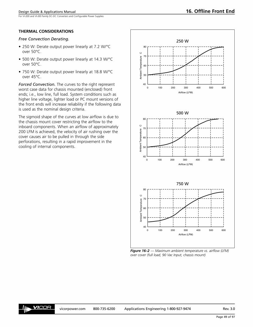
Design Guide & Applications ManualFor VI-200 and VI-J00 Family DC-DC Converters and Configurable Power Supplies
vicorpower.com 800-735-6200 Applications Engineering 1-800-927-9474 Rev. 3.0
Page 49 of 97
THERMAL CONSIDERATIONS
Free Convection Derating.
• 250 W: Derate output power linearly at 7.2 W/°C over 50°C.
• 500 W: Derate output power linearly at 14.3 W/°C over 50°C.
• 750 W: Derate output power linearly at 18.8 W/°C over 45°C.
Forced Convection. The curves to the right representworst case data for chassis mounted (enclosed) frontends; i.e., low line, full load. System conditions such ashigher line voltage, lighter load or PC mount versions ofthe front ends will increase reliability if the following datais used as the nominal design criteria.
The sigmoid shape of the curves at low airflow is due tothe chassis mount cover restricting the airflow to theinboard components. When an airflow of approximately200 LFM is achieved, the velocity of air rushing over thecover causes air to be pulled in through the sideperforations, resulting in a rapid improvement in thecooling of internal components.
250 W
500 W
750 W
40
80
70
60
50
5004003002001000
Airflow (LFM)
Am
bien
t Tem
pera
ture
C
600
40
80
70
60
50
5004003002001000
Airflow (LFM)
Am
bien
t Tem
pera
ture
C
600
40
80
70
60
50
6005004003002001000
Airflow (LFM)
Am
bien
t Tem
pera
ture
C
Figure 16–2 — Maximum ambient temperature vs. airflow (LFM)over cover (full load, 90 Vac Input, chassis mount)
16. Offline Front End

Design Guide & Applications ManualFor VI-200 and VI-J00 Family DC-DC Converters and Configurable Power Supplies
vicorpower.com 800-735-6200 Applications Engineering 1-800-927-9474 Rev. 3.0
Page 50 of 97
3-PHASE FRONT ENDS
Vicor’s 3-phase front-ends are available as chassis mountproducts that deliver reliable DC bus voltage to VI-x6xFamily (nominal 300 Vdc input) converters up to 1.5 kW, 3 kW and 5 kW.
Front ends operate from 3-phase (4-wire delta or 4 or 5-wire wye) AC mains input and provide conducted EMCfiltering to VDE/FCC Class A, transient surge protection,inrush current limiting and ENABLE output suitable forcontrolling an array of Vicor converters via the GATE IN
pin. Isolated AC-OK and BUS-OK outputs are also providedfor advance warning of DC bus dropout due to AC linefailure and indication of internal DC bus integrity in theuser system, respectively.
These front ends have been designed to comply with the requirements of major safety agencies when used inconjunction with the recommended mains switching andinput fusing.
+V<70 V
ACMAINS
Vdc–Vdc+
MOD ENBL
AC-OK –AC-OK +
BUS-OK +BUS-OK –L3
L2
L1
N
GND
+INGATE IN
–IN
VI-x6xModule
+INGATE IN
–IN
VI-x6xModule
F2
F3
F4
Fn
Vce sat.<0.4 V@ 1.5 mA
+V<70 V
EARTH GROUND
+INGATE IN
–IN
VI-x6xModule
+INGATE IN
–IN
VI-x6xModule
+V<70 V
Vdc–
Vdc+
AC-OK –AC-OK +
BUS-OK +BUS-OK –
L3L2L1N
GND
F2
F3
F4
Fn
Vce sat.<0.4V@ 1.5 mA
+V<70 V
MOD ENBL
ACMAINS
EARTHGROUND
+INGATE IN
–IN
VI-x6xModule
+INGATE IN
–IN
VI-x6xModule
+INGATE IN
–IN
VI-x6xModule
+INGATE IN
–IN
VI-x6xModule
CAUTION: External capacitors connected to +Vdc and –Vdc willsignificantly increase inrush current. Also these capacitors aresubject to AC ripple voltages of approximately 40 V at full load.
CAUTION: External capacitorsconnected to +Vdc and –Vdc will significantly increase inrushcurrent. Also these capacitors aresubject to AC ripple voltages ofapproximately 40 V at full load.
Ground all baseplates to Earth Ground [a]
16. Offline Front End
Figure 16–3 — 1.5, 3.0 kW Front-end
Figure 16–4 — 5.0 kW Front-end
Ground All Baseplates to Earth Ground [a]
[a] To control EMC most effectively, the return path toground from either the front-end or modules should be madevia a good RF ground (i.e., a braided wire) if possible.
[a] To control EMC most effectively, the return path toground from either the front-end or modules should be madevia a good RF ground (i.e., a braided wire) if possible.
NOTE: x,y capacitors not shown for clarity
NOTE: x,y capacitors not shown for clarity

Design Guide & Applications ManualFor VI-200 and VI-J00 Family DC-DC Converters and Configurable Power Supplies
vicorpower.com 800-735-6200 Applications Engineering 1-800-927-9474 Rev. 3.0
Page 51 of 97
FUSING INFORMATION
• 1.5 kW front end: 7 A / 250 V normal blow in all three phases of the AC line (Bussman ABC-7 or Littlefuse 314-007).
• 3 kW front end: 12 A / 250 V normal blow in all three phases of the AC line (Bussman ABC-12 or Littlefuse 314-012).
• 5 kW front end: 20 A / 250 V normal blow in all three phases of the AC line (Bussman ABC-20).
ENVIRONMENTAL DATA
• Operating temperature (no load to full load): –20˚C to +50˚C, free convection
• Non operating temperature: –40˚C to +80˚C
• Operating / non-operating humidity: 95% relative, non-condensing
ELECTRICAL DATA — AC LINE INPUT VOLTAGECONNECTIONS (PHASE TO PHASE)
• 3-phase delta (4 wire): 208 Vac (nominal) +20% / –10%.Connect the three phases (L1, L2, L3) and GND (earth) to the five terminal barrier block marked as such.
• 3-phase wye distribution (5-wire): 208 Vac (nominal) +20% / –10%. Connect the three phases (L1, L2, L3), N (neutral), and GND (earth) to the five terminal barrier block marked as such.
• Line frequency: 47 – 440 Hz
DC OUTPUT CONNECTIONS AND MODULE ENABLE
A three terminal barrier block labeled Vdc–, Vdc+ andMOD EN provides both the DC input enable and enablecontrol line for Vicor converters.
• Vdc–: Negative DC input terminal to all Vicor converters.
• Vdc+: Positive DC input terminal to all Vicor converters.
• MOD EN: Connect to the GATE IN terminal of all Driver modules. This connection must be made to guarantee proper enabling of the converter array on power-up and proper shut down of the converter array on power loss, loss of phase or output fault.
CAUTIONS
• This product is designed to operate with Vicor VI-x6x Family (300 Vdc input) converters, Mega Modules and the 300 Vin Maxi, Mini and Micro converters.
• This product is not intended for use with European 380 – 415 Vac three phase distribution.
• This product is an offline AC-DC power supply. It is not isolated from the AC mains.
• Proper grounding is mandatory for safe operation.
16. Offline Front End

Design Guide & Applications ManualFor VI-200 and VI-J00 Family DC-DC Converters and Configurable Power Supplies
vicorpower.com 800-735-6200 Applications Engineering 1-800-927-9474 Rev. 3.0
Page 52 of 97
17. DC Input Power System (ComPAC/MI-ComPAC Family)
OVERVIEW
The ComPAC is a low profile, highly efficient, high densityconfigurable DC-DC power solution with EMC filtering,transient protection and reverse polarity protection. It hasan isolated master disable input for remote shutdown, andprovides outputs from 1 – 95 Vdc and power-up to 600 W.
There are five input voltages available which comply withtelecommunication and industrial control EMC specifications.Refer to data sheet for applicable standards at vicorpower.com.
There are two military input voltages available which complywith military EMC specifications and the transient and spikespecifications. Refer to data sheet for applicable standards at vicorpower.com.
ComPACs can be configured in 1-up, 2-up or 3-uppackages with total output power limited to themaximum power of individual VI-200 or MI-200 seriesconverters. Output voltages may be trimmed by the user.
Output Power. The maximum total power which isdelivered from the ComPAC is:
Weight.1-Up: 1.2 lbs (540 g)2-Up: 2.4 lbs (1,080 g)3-Up: 3.6 lbs (1,630 g)
Operating Case Temperature.E-Grade: –10˚C to +85˚CC-Grade: –25˚C to +85°CI-Grade: –40˚C to +85°CM-Grade: –55˚C to +85°C
Overall Efficiency. The overall efficiency of the ComPAC isapproximately 1% less than the efficiency of the Vicor DC-DC converters (typical efficiencies: 77% for 2 V output,81% for 5 V output and 83% for 12 – 48 V output).
EMC Performance, Conducted EMC. The ComPAC willconform to the following conducted EMC specificationson the input power leads:
• Telecom (24 V, 48 V inputs): Bellcore TR-TSY-000513, Issue 2 July 1987 and Rev. 1, December 1988.British Telecom Document BTR2511, Issue 2.
• Commercial (300 V input): FCC Pt. 15 Subpt. J, Class A / VDE 0871 Class A.
• Military (28 V, 270 V): MIL-STD-461C Conducted Emissions: CE01, CE03, CE07 Conducted Susceptibility: CS01, CS02, CS06
Radiated EMC. The ComPAC will conform to thefollowing radiated specifications:
• Military: Radiated Emissions: RE02; Radiated Susceptibility: MIL-STD-461C, RS02, RS03.
Input Transient Protection. The input transientprotection will suppress short term transients appearingon the input line. Refer to data sheet for applicablestandards at vicorpower.com.
Input Surge Withstand. The 24 V, 48 V and 300 V inputComPAC shall withstand, without damage or interruptionof power, an input line surge shown below for a durationof 100 ms from a source impedance of 500 milliohms.
Extended Input OV Shut Down. Surge protection shallalso shut down the ComPAC in the presence of sustainedinput surges (100 – 1,000 ms) which would causeexcessive dissipation or damage. The ComPAC will autorestart when the input overvoltage is removed.
Input Reverse Polarity Protection. The ComPAC’s inputis protected against reverse polarity. No damage will occurprovided that external current limiting is present (i.e., fuse).
Output Short Circuit Protection. Output short circuitprotection is provided by the current limiting of the VicorDC-DC converters.
Undervoltage Lockout. The ComPAC incorporates anundervoltage lockout which will inhibit the output of allconverters until the input line exceeds the brownoutvoltage specified for the converter input range.
Following startup, the undervoltage lockout will inhibit theconverter output(s) should the input drop roughly 8 – 10 V below the UV lockout limits stated above.
28 V 2 18 – 50270 V 6 125 – 400
Nominal Input Input VoltageInput Voltage Designator Range
24 V and 24 V (wide) 150 W 300 W 450 W28 V, 270 V (military) 100 W 200 W 300 W48 V and 48 V (wide), 300 V 200 W 400 W 600 W
Nominal Total Output PowerInput Voltage 1-Up 2-Up 3-Up
24 V 1924 V (wide) 17
28 V (military) 1748 V 41
48 V (wide) 35270 V (military) 121
300 V 188
Nominal UV LockoutInput Voltage (Vdc, Typical)
24 V 1 21.7 – 3224 V (wide) W 18.7 – 36
48 V 3 42 – 6048 V (wide) N 36 – 76
300 V 6 200 – 400
Nominal Input Input VoltageInput Voltage Designator Range

Design Guide & Applications ManualFor VI-200 and VI-J00 Family DC-DC Converters and Configurable Power Supplies
vicorpower.com 800-735-6200 Applications Engineering 1-800-927-9474 Rev. 3.0
Page 53 of 97
RECOMMENDED INPUT LINE FUSING
The ComPAC must be fused externally. The table belowlists the fuse ratings for one, two and three-up units(maximum output 200, 400 and 600 W).
RECOMMENDED INPUT WIRING AND TORQUE
RECOMMENDED OUTPUT WIRING
Use the output wire gauge that corresponds to the outputcurrent of the ComPAC unit:
Long cable runs, or wires in large bundles will requireheavier cable to avoid excessive voltage drops or overheating.
GROUNDING
For safe operation, the ComPAC unit must be grounded.Connect a ground lead to the terminal marked (GND). Usethe same wire gauge as that specified for your ComPACunit’s input voltage connections.
MASTER DISABLE
The ComPAC incorporates an optically isolated MasterDisable input which will shut down the ComPAC outputwhen a current is driven through the disable terminals.
DISABLE CURRENT
• 4 mA DC minimum for 1-up ComPAC• 8 mA DC minimum for 2-up ComPAC• 12 mA DC minimum for 3-up ComPAC
TRIMMING
The nominal output voltage of the ComPAC can beadjusted from 110% to 50% of nominal voltage. Refer toOutput Voltage Trimming, Section 5, for external resistorvalues. DO NOT trim the outputs higher than 110% oftheir nominal output power (output overvoltage protectionmay trigger). When the output is trimmed up, do notexceed its maximum rated output power.
NOTE: 10 V, 12 V, and 15 V outputs, standard trimrange ±10%, 3.3 V output trim range 2.20 to 3.63 V.
REMOTE SENSING
+SENSE and –SENSE must be connected locally or remotely.
OUTPUT TERMINAL CONNECTIONS
A hardware kit with parts for output terminal connections isprovided with each ComPAC unit. The following drawingshows the assembly of those parts for the properconnection of metal power terminals. Assembly for PCBpower terminals is the same except that they do not requirean external tooth lockwasher. See Figure 17–2 for therecommended torque level for each stud size.
17. DC Input Power System (ComPAC/MI-ComPAC Family)
20 mA Max.
Disable
DIS+
DIS–
+
V
Figure 17–1 — ComPAC module disable
EXTERNAL TOOTHLOCKWASHER
#10 TERMINALRETAINING NUT
#10 NUT PLATE
USER OUTPUTTERMINALS
#10 BRASS STUD
HELICALLOCKWASHER(FITS WITHIN
OPENING PROVIDED)
TERMINAL COVERNEGATIVE
Figure 17–2 — Output terminal connections
24 V 10 A /32 V 20 A /32 V 30 A /32 V 24 V (wide) 12 A /32 V 20 A /32 V 30 A /32 V28 V (military) 10 A /250 V 20 A / 250 V 30 A /125 V48 V 8 A /60 V 15 A /60 V 25 A /60 V48 V (wide) 6 A /100 V 15 A /100 V 25 A /100 V270 V (military) 2 A /250 V 4 A /250 V 6 A /250 V300 V 2 A /250 V 4 A /250 V 6 A /250 V
Nominal Fuse RatingInput Voltage 1-Up 2-Up 3-Up
1-Up #16 AWG 10 in-lb2-Up #14 AWG 15 in-lb
105 A – 160 A: #4 26 A – 40 A: #10 7 A – 10 A: #1666 A – 104 A: #6 16 A – 25 A: #12 4 A – 6 A: #1841 A – 65 A: #8 11 A – 15 A: #14 0 A – 3 A: #20
–OUT, +OUT TerminalsLC, PC, RC Series PCB 8-32 UNC 10 in-lbs (1.1 N-m)MC and NC Series Metal 10-32 UNC 15 in-lbs (1. 7 N-m)
QC Series PCB 8-32 UNC 10 in-lbs (1.1 N-m)Metal 10-32 UNC 15 in-lbs (1.7 N-m)
+ / – SENSE, TRIM TerminalsAll Models Sized to accept Amp Faston© insulated
receptacle #2-520184-2.
Terminal and Terminal Stud RecommendedProduct Model Style Size Torque

Design Guide & Applications ManualFor VI-200 and VI-J00 Family DC-DC Converters and Configurable Power Supplies
vicorpower.com 800-735-6200 Applications Engineering 1-800-927-9474 Rev. 3.0
Page 54 of 97
THERMAL DATA
Operating Ambient Temperature. Depends on factorssuch as output power, availability of forced air, andmounting technique. DO NOT allow the ComPAC toexceed its maximum operating temperature, which isreached when the case is 85˚C. Temperature measured atcenter of heat sink. (Full power can be delivered up to thistemperature.) Refer to Section 20, Thermal Curves, todetermine the maximum ambient temperature for yourapplication.
NOTE: To ensure proper heat transfer from theinternal module(s) to the heat sink, the mountingholes through the heat sink must be properlytorqued at all times during operation. If the unit isoperated unmounted, insert a #6 or metric M3.5flathead screw through each hole from below andsecure with a nut on top, torqued to 6 lb-in (0.83 N-m).
Thermal Impedance, Free Convection.Thermal resistance baseplate to air (˚C/W):
Forced Convection. Thermal resistance baseplate to air(horizontal mount):
NOTE: A 1.37" (34,8 mm) heat sink, option H1, is also available.
17. DC Input Power System (ComPAC/MI-ComPAC Family)
Vertical 2.44 1.17 0.76Horizontal 3.60 1.70 1.35
Type ofMounting 1-Up 2-Up 3-Up
3.6 1.7 1.35 02.7 1.4 1.26 502.3 1.3 1.11 1001.6 0.97 0.82 2501.15 0.70 0.58 5000.9 0.54 0.46 7500.78 0.45 0.38 1,000
Thermal Resistance (°C/W)Airflow (LFM)1-Up 2-Up 3-Up

Design Guide & Applications ManualFor VI-200 and VI-J00 Family DC-DC Converters and Configurable Power Supplies
vicorpower.com 800-735-6200 Applications Engineering 1-800-927-9474 Rev. 3.0
Page 55 of 97
OVERVIEW
Vicor’s FlatPAC consists of an offline single phase AC frontend and one, two or three VI-26x / VI-B6x Family DC-DCconverter modules (1-up, 2-up, 3-up), combined in anintegrated mechanical assembly. This assembly provides acomplete, high efficiency, offline switching power supplydelivering power up to 600 W. The offline front endprovides rectification and filtering of the AC input,delivering a nominal unregulated 300 Vdc bus as input tothe VI-26x / VI-B6x Family converter modules. The frontend control circuit will automatically strap the bridge as avoltage doubler for 115 Vac operation or as a full bridgefor 230 Vac operation.
CIRCUIT OPERATION
AC line voltage is applied via an agency-approved terminalblock providing AC mains (L1, L2/N and GND). Current inthe L1 lead is applied to a 15 A / 250 V fuse for the 3-upFlatPAC, a 12 A / 250 V fuse for the 2-up FlatPAC and a 8 A / 250 V fuse for the 1-up FlatPAC. This current isinterrupted only in the event of a catastrophic failureof a main power component internal to the FlatPAC.
The input current beyond the fuse is passed through anEMC filter designed to meet conducted noise limits ofFCC Part 15 EN55022 Class B for the 2-up and 3-upversions. At start-up, AC inrush current is limited by a PTC thermistor prior to being passed to the main energystorage capacitors. This PTC thermistor serves as both aninrush current limiter on power-up and a current limitingshutdown device in the event of a line overvoltagecondition. The PTC is shunted out shortly after initialpower-up by a pair of inverse parallel SCRs on the 3-upFlatPAC (TRIAC for the 1-up and 2-up FlatPAC), controlledby an opto-TRIAC coupler driven by a DC bus voltagesense circuit. The main rectifiers and filter capacitors arearranged in a conventional selectable configuration andact as either a full wave bridge or voltage doubler,delivering a nominal 300 Vdc to the converter modules.
At initial power-up, the front end is configured for 230 Voperation and the PTC inrush limiter permits the mainstorage capacitors to charge up at a controlled ratetoward full operating DC bus potential. If the bus voltageis below the operating threshold for the converter, theunit will autostrap for 115 V operation. The autostrappingfunction is performed by a control circuit and TRIAC (dualSCRs on 3-up unit) which configures the front end from afull wave bridge to a voltage doubler. Once the unitautostraps for 230 V operation, it will be necessary torecycle the AC power to allow operation at 115 V. If theunit is operating in the 115 V mode and a long durationtransient is applied to the FlatPAC (>150 Vac for 50 ms),the unit will autostrap for 230 V operation.
The control circuit maintains the converter GATE IN pinslow, the PTC shunt inactive and the AC-OK and BUS-OKoutputs in FAIL status until the DC bus potential reaches aminimum threshold at which full power and hold-up canbe delivered. The GATE IN terminals of all Driver modulesinternal to the FlatPAC are FET-controlled by a logicalreplica of the BUS-OK status line, and as such will inhibitconverter operation at power-up until the DC bus potentialhas settled to full operating level. The converters are thenenabled and the PTC shunt activated.
The AC-OK and BUS-OK status lines go to their respectiveactive states almost simultaneously on initial power-up.AC-OK will de-assert prior to BUS-OK on loss of AC input,providing advance warning of impending DC failure shouldthe AC line not return prior to the expiration of the ride-through time (a function of both load and line voltage).
The front-end output is bled down automatically after lossof AC input, as the logic circuit operating power is derivedfrom a bleed path across the DC output bus. Wait twominutes before reapplying input after shutdown. Inputvoltage to the converters is made via fast-acting 3 A / 250V Buss PC-Tron fuses in each positive input lead. The fusewill clear rapidly and protect the front-end from damagein the event of a module input short.
Input overvoltage sensing and protection is performed bya voltage sensing circuit connected across the DC bus. Inthe event of an overvoltage condition, a SCR / PTCcombination will simultaneously disable the drive for theTRIAC / SCR PTC shunt, disable the converters and apply aload across the DC bus. Normal operation resumes whenthe input voltage falls within the normal operating rangewhen operated from a 230 Vac source.
A Master Disable function is incorporated in the 2-up and3-up FlatPAC (MOD DIS+, MOD DIS–). This opticallyisolated input will disable the output of all converterssimultaneously. Applying a current to this input willdisable the converters. This disable current should belimited to 30 mA maximum by an external control element.
FLATPAC AC-OK AND BUS-OK STATUS OUTPUTS,MOD-DIS INPUT (2-UP AND 3-UP ONLY)
The BUS-OK and AC-OK outputs provide the user withboth an optically isolated status indication of the internalDC bus condition and advance warning of pending DCbus drop-out due to AC line loss. These outputs, in systemapplications, can provide power supply status, switch in(standby) backup sources or initiate “power-down”sequences to save volatile memory contents in the eventof AC line loss. The MOD-DIS input is an optically coupled
18. AC Input Power System (FlatPAC Family)

Design Guide & Applications ManualFor VI-200 and VI-J00 Family DC-DC Converters and Configurable Power Supplies
vicorpower.com 800-735-6200 Applications Engineering 1-800-927-9474 Rev. 3.0
Page 56 of 97
input and allows for remote disabling of the outputs of 2-up and 3-up FlatPACs.
BUS-OK. An internal replica of BUS-OK is wired to theGATE IN input of all internal Driver modules. The moduleswill be disabled (no DC output) during initial power-up ofthe FlatPAC until the internal DC input bus voltage to theDC-DC converters is sufficient to support fully-loadedoperation. The BUS-OK status output reflects the status ofthis inhibit function. This same logic circuit will shut downthe converters when the internal DC bus voltage isinsufficient to support proper loaded operation. This shutdown will occur during normal power down, AC linedropouts of duration exceeding the hold-up time, orinternal faults causing the internal DC bus voltage at theinput of the converters to collapse.
AC-OK. This output is provided primarily as an advancewarning of a potential DC BUS-OK shut down due to lossof AC line or an internal fault. A minimum advancewarning time of 5 ms is provided at 90 Vac and full load.
MOD-DIS+, MOD-DIS–
The Module Disable function will disable the output(s) ofthe 2-up and 3-up FlatPACs. The supply is disabled byapplying current to the MOD-DIS+ / MOD-DIS– input. Theminimum input current for disabling the supplies is 1 mA.The maximum allowable current is 30 mA.
ELECTRICAL CONNECTIONS
Status output pairs AC-OK+, AC-OK– and BUS-OK+, BUS-OK– are the collectors (+) and emitters (–) of NPNoptoisolator output transistors (one optoisolator per statussignal). The collector terminals AC-OK+ and BUS-OK+ ofthe optocouplers, in a typical application, can beconnected via current limiting resistors to a source nogreater than 70 Vdc. These resistors should limit themaximum current to the optocoupler output transistors to1.5 mA. The emitter terminals AC-OK– and BUS-OK– areconnected to the return of the external source. The statusOK condition will set the optocoupler output transistors insaturation and are capable of sinking up to 1.5 mA with aVce saturation voltage of 0.4 V. Users should be cautionedthat although the output of the FlatPAC can be used asthe pull-up source, shortly after BUS-OK changes from OK(saturated) to NOT OK (high Z), the pull-up voltage will beshut down. It is thus advisable to provide a capacitivereservoir, if the pull-up source is one of the FlatPAC’soutputs, in order to maintain the pull-up potential afterloss of DC current output. Use edge sensing logic to
detect assertion of logic outputs, or a separate source ofbias supply voltage (i.e., backup batteries) to provide asafe pull-up voltage source regardless of the AC line status.
MOD-DIS Input. Apply a current of 1 – 30 mA to disableoutput. Forward voltage drop of internal opto diode is1.65 V max. at 30 mA max.
AC-OK and BUS-OK Status Outputs. Outputs low whenOK. Vce sat. = < 0.4 V @ 1.5 mA. Maximum externalpullup is 70 Vdc. AC-OK and BUS-OK signals are isolatedand can have different reference levels.
18. AC Input Power System (FlatPAC Family)
MOD-DIS –MOD-DIS +AC-OK –AC-OK +BUS-OK –BUS-OK +
InternalSupervisoryCircuits(Optocouplers)
AC Mains
Earth Ground
L1
L2/N
GND
2-Upand3-Up
1-Up
Figure 18–1 — AC mains and supervisory connections
NOTE: Product is internally fused
Figure 18–2 — External supervisory functions (2-up and 3-upmodels only)
V+
r
AC-OK
+
–
1.5 mAmax.
V
+r
BUS-OK
+
–
30 mA max.
Disable
MOD-DIS
V
+
+
–
1.5 mAmax.
FlatPAC

Design Guide & Applications ManualFor VI-200 and VI-J00 Family DC-DC Converters and Configurable Power Supplies
vicorpower.com 800-735-6200 Applications Engineering 1-800-927-9474 Rev. 3.0
Page 57 of 97
Fusing. The FlatPAC’s internal fuses are not user-replaceable.Please return the unit to vendor if servicing is necessary.
Grounding. To satisfy IEC950 Class I grounding requirements,connect a ground lead to the terminal marked (GND).For 1-up FlatPAC models (max. output 200 W), use 1.5 mm2
/ #16 AWG wire; for 2-up and 3-up models (max. output400 W and 600 W), use 2.5mm2 / #14 AWG wire.
Input Voltage Connections. Connect the line voltage to L1 (hot) and L2N (neutral). For 1-up FlatPAC models(max. output 200 W), use #16 AWG input wire; for 2-upand 3-up models (max. output 400 W and 600 W), use #14AWG input wire. Recommended connector screw torque is5 to 7 in-lbs (0.5 to 0.8 N-m). Recommended strip length is8 mm. Use your FlatPAC model only with the correspond inginput voltages and frequencies shown in the table below.
Output Wire Gauge. Use the output wire gauge thatcorre sponds to the output current of your AutorangingFlatPAC unit, below: Do not loosen bottom nut.
Long cable runs, or wires in large bundles will requireheavier cable to avoid excessive voltage drops or overheating.
Output Voltage Trimming. Do not trim the outputshigher than 110% of their nominal output voltage. Whenan output is trimmed up, do not exceed its maximumrated output power. (refer to Section 5)
Operating Temperature. Do not allow the FlatPAC toexceed its maximum operating temperature, which isreached when the heat sink is 85°C. (Full power can bedelivered up to this temperature.) Heat sink temperature isa function of the output power and voltage of the supply,ambient temperature, and airflow across the heat sink.Always use worst-case conditions when calculatingoperating temperature.
NOTE 1: To ensure proper heat transfer from theinternal module(s) to the heat sink, the mountingholes through the heat sink (two, three, and fourholes on 1-up, 2-up, and 3-up models, respectively)must contain torqued screws at all times duringoperation, whether or not the unit is mounted. If theunit is operated unmounted, insert a #6 or M3.5panhead screw through each hole from below andsecure with a nut on top, torqued to 6 in-lbs (0.7 N-m).
NOTE 2: All FlatPAC models are available with aconduction cooled flat plate instead of the top heatsink. Go to vicorpower.com for outline drawings.
Input / Output Retrofit Connections. A hardware kit,available from Vicor, allows the input and outputsupervisory terminals to be connected in the same manneras for the earlier style FlatPAC (2-up model only). Theretrofit output terminals are sized to accept AMP Faston®
insulated receptacle #2-520184-2.
18. AC Input Power System (FlatPAC Family)
T1 – T0 0 0.1 1.0 msT3 – T2 0 – – ms Ride-through time
T4 – T2 5 – – ms Hold-up time
T4 – T3 5 – – ms AC fail warning time
Time Interval Min Typ Max Units Notes
Figure 18–3 — Timing diagram – status signals (2-up and 3-upmodels only)
VLINE > 90 (180)Vac
AC LineInterrupted
ACLine
AC-OK
BUS-OK
T0 T1 T2 T3 T4
Conditions: Full Load 90 (180)Vac, AC Line
R1 (KΩ) 0.953 15.8 22.1 41.2 48.7 90.9 +10%, –10%
R2 (KΩ) 90 90 90 90 90 90 +10%, –10%
Resister Values for Trimming Standard Output VoltagesNom. Output
5 V 12 V 15 V 24 V 28 V 48 VTrim
Voltage Range
Figure 18–4 — Output SENSE and TRIM (all models with VI-200s)
R2
10K
R1
+ VOUT
VOUT RTN
+OUT
+SENSETRIM
–SENSE
–OUT
NOTE: +SENSE and –SENSE must be connected locally orremotely (shown).
Load
+
–
BatteryCharger
ExternalControlFunctions
Programmable Currentor Voltage Source
12 – 48 VBattery
+
–
+OUT
VTRIMITRIMIMON
–OUT
ExternalControlFunctions
+OUT
VTRIMITRIMIMON
–OUT
Figure 18–5 — Typical applications (models with BatMods only)
C-Grade VI-xU-Cx 47 – 63 Hz 47 – 63 HzI-Grade VI-xU-Ix 47 – 440 Hz 47 – 440 Hz
Product Grade Model 90 – 132 Vac 180 – 264 Vac
100A–160A: #2AWG 30A–50A: #8AWG 10A–15A: #14 AWG75A –100A: #4 AWG 20A–30A: #10AWG 6A–10A: #16 AWG50A –75 A: #6 AWG 15A –20 A:#12AWG 0 A – 6 A: #18 AWG
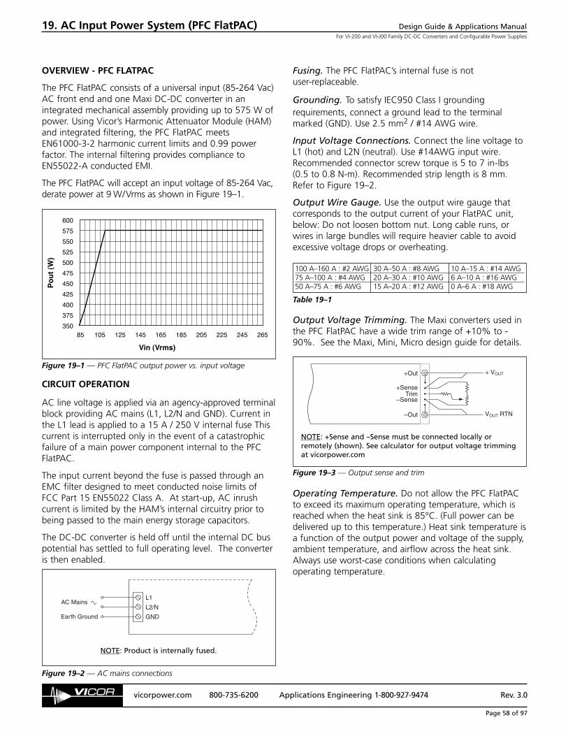
Design Guide & Applications ManualFor VI-200 and VI-J00 Family DC-DC Converters and Configurable Power Supplies
vicorpower.com 800-735-6200 Applications Engineering 1-800-927-9474 Rev. 3.0
Page 58 of 97
19. AC Input Power System (PFC FlatPAC)
OVERVIEW - PFC FLATPAC
The PFC FlatPAC consists of a universal input (85-264 Vac)AC front end and one Maxi DC-DC converter in anintegrated mechanical assembly providing up to 575 W ofpower. Using Vicor’s Harmonic Attenuator Module (HAM)and integrated filtering, the PFC FlatPAC meets EN61000-3-2 harmonic current limits and 0.99 powerfactor. The internal filtering provides compliance toEN55022-A conducted EMI.
The PFC FlatPAC will accept an input voltage of 85-264 Vac,derate power at 9 W/Vrms as shown in Figure 19–1.
CIRCUIT OPERATION
AC line voltage is applied via an agency-approved terminalblock providing AC mains (L1, L2/N and GND). Current inthe L1 lead is applied to a 15 A / 250 V internal fuse Thiscurrent is interrupted only in the event of a catastrophicfailure of a main power component internal to the PFCFlatPAC.
The input current beyond the fuse is passed through anEMC filter designed to meet conducted noise limits ofFCC Part 15 EN55022 Class A. At start-up, AC inrushcurrent is limited by the HAM’s internal circuitry prior tobeing passed to the main energy storage capacitors.
The DC-DC converter is held off until the internal DC buspotential has settled to full operating level. The converteris then enabled.
Fusing. The PFC FlatPAC’s internal fuse is not user-replaceable.
Grounding. To satisfy IEC950 Class I groundingrequirements, connect a ground lead to the terminalmarked (GND). Use 2.5 mm2 / #14 AWG wire.
Input Voltage Connections. Connect the line voltage toL1 (hot) and L2N (neutral). Use #14AWG input wire.Recommended connector screw torque is 5 to 7 in-lbs(0.5 to 0.8 N-m). Recommended strip length is 8 mm.Refer to Figure 19–2.
Output Wire Gauge. Use the output wire gauge thatcorresponds to the output current of your FlatPAC unit,below: Do not loosen bottom nut. Long cable runs, orwires in large bundles will require heavier cable to avoidexcessive voltage drops or overheating.
Output Voltage Trimming. The Maxi converters used inthe PFC FlatPAC have a wide trim range of +10% to -90%. See the Maxi, Mini, Micro design guide for details.
Operating Temperature. Do not allow the PFC FlatPACto exceed its maximum operating temperature, which isreached when the heat sink is 85°C. (Full power can bedelivered up to this temperature.) Heat sink temperature isa function of the output power and voltage of the supply,ambient temperature, and airflow across the heat sink.Always use worst-case conditions when calculatingoperating temperature.
AC Mains
Earth Ground
L1
L2/N
GND
Figure 19–2 — AC mains connections
NOTE: Product is internally fused.
+Out
+SenseTrim
–Sense
–Out
+ VOUT
VOUT RTN
NOTE: +Sense and –Sense must be connected locally or remotely (shown). See calculator for output voltage trimming at vicorpower.com
Figure 19–3 — Output sense and trim
350
375
400
425
450
475
500
525
550
575
600
85 105 125 145 165 185 205 225 245 265
Vin (Vrms)
Po
ut
(W)
Figure 19–1 — PFC FlatPAC output power vs. input voltage
100 A–160 A : #2 AWG 30 A–50 A : #8 AWG 10 A–15 A : #14 AWG75 A–100 A : #4 AWG 20 A–30 A : #10 AWG 6 A–10 A : #16 AWG50 A–75 A : #6 AWG 15 A–20 A : #12 AWG 0 A–6 A : #18 AWG
Table 19–1

Design Guide & Applications ManualFor VI-200 and VI-J00 Family DC-DC Converters and Configurable Power Supplies
vicorpower.com 800-735-6200 Applications Engineering 1-800-927-9474 Rev. 3.0
Page 59 of 97
NOTE 1: To ensure proper heat transfer from the internalmodules to the heat sink, the mounting holes through theheat sink (three holes on 2-up models) must containtorqued screws at all times during operation, whether ornot the unit is mounted. If the unit is operatedunmounted, insert a #6 or M3.5 panhead screw througheach hole from below and secure with a nut on top,torqued to 6 in-lbs (0.7 N-m).
NOTE 2: All PFC FlatPAC models are available with aconduction cooled flat plate instead of the top heat sink.Go to vicorpower.com for outline drawings. Refer toFigure 19–4 for additional deratings for the -cc variants.
19. AC Input Power System (PFC FlatPAC)
0
100
200
300
400
500
600
20 25 30 35 40 45 50 55 60 65 70 75 80 85
Ambient Temperature (°C)
Ou
tpu
t P
ow
er (
W)
80
6070
50
Cold Plate Temp (°C)
300
350
400
450
500
550
600
85 110 135 160 185 210 235 260
Input Voltage (Vac)
Ou
tpu
t P
ow
er (
Wat
ts)
Figure 19–4 — Power de-rating conduction cooled option Figure 19–5 — Output power start-up de-rating @ –30° C (I-Grade only). 5 minute warm up required before full power (seeFigure 19–1) is available.

Design Guide & Applications ManualFor VI-200 and VI-J00 Family DC-DC Converters and Configurable Power Supplies
vicorpower.com 800-735-6200 Applications Engineering 1-800-927-9474 Rev. 3.0
Page 60 of 97
OVERVIEW
Simplified thermal management is one of the benefits ofusing Vicor converters. High operating efficiency minimizesheat loss, and the low profile package features an easilyaccessible, electrically isolated thermal interface surface.
Proper thermal management pays dividends in terms ofimproved converter and system MTBFs, smaller size andlower product life-cycle costs. The following pages provideguidelines for achieving effective thermal management ofVicor converters.
EFFICIENCY AND DISSIPATED POWER
A DC-DC converter takes power from an input source andconverts it into regulated output power for delivery to aload. Not all of the input power is converted to outputpower however; some is dissipated as heat within theconverter. The ratio of delivered output power toconverter input power is defined as the converter’sefficiency. Efficiency is a basic figure of merit that can beused to relate power dissipation directly to converteroutput power, as illustrated in Figures 20–1a and 20–1b.
The first step in evaluating cooling requirements is tocalculate worst-case dissipation based on converterefficiency and worst-case anticipated load power. Clearly,higher efficiency will translate into lower power dissipationand simplify the cooling problem. Vicor converters areamong the most efficient converters available, with fullload efficiencies typically in excess of 80%.
REMOVING HEAT FROM VICOR CONVERTERS
Heat is removed from Vicor converters through the flatmetal baseplate on top of the module. The baseplate isthermally coupled to, but electrically isolated from, allinternal heat-generating components. The basic thermaldesign problem is to transfer heat from the baseplate intothe surrounding environment as a means of maintainingbaseplate temperature at or below rated maximum.
Heat energy is transferred from regions of high temperatureto regions of low temperature via three basic mechanisms;radiation, conduction and convection.
Radiation. Electromagnetic transfer of heat between masses at different temperatures.
Conduction. Transfer of heat through a solid medium.
Convection. Transfer of heat through the medium of a fluid; typically air.
All three of these heat transfer mechanisms are active tosome degree in every application. Convection will be thedominant heat transfer mechanism in most applications.Nondominant effects will provide an added contributionto cooling; in some cases, however, they may result inundesirable and unanticipated thermal interactionsbetween components and subassemblies.
All three of these mechanisms should be given considerationwhen developing a successful cooling strategy.
RADIATION
Radiant heat transfer occurs continuously between objectsat different temperatures that are exposed to each other.The net effect on the temperature of an individual part isdependent on a great many factors, including its temperaturerelative to other parts, relative part orientations, surfacefinishes and spacing. The difficulty in quantifying many ofthese factors, combined with the universal presence ofradiant energy exchange, makes calculation of radiationaltemperature effects both a complex and generallyimprecise task.
92%
88%
84%
80%
20% 50% 75% 100%
12 V, 15 V, 24 V and 48 V Models
5 V Models
Percentage of Load
Efficiency
Load
+
–
InputSource
Power Input = Power Dissipated as Heat + Power Output
Power Dissipated = Power Output X
Power Input x Efficiency (η) = Power Output
1n )) –1
20. Thermal and Module Mounting Considerations
Figure 20–1a — Module efficiency
Figure 20–1b — Dissipated power

Design Guide & Applications ManualFor VI-200 and VI-J00 Family DC-DC Converters and Configurable Power Supplies
vicorpower.com 800-735-6200 Applications Engineering 1-800-927-9474 Rev. 3.0
Page 61 of 97
Temperature differentials encountered in practicalapplications of Vicor converters are never large enough to cause radiational cooling to be the dominant heattransfer mechanism. Radiation will account for less than10% of total heat transfer in the majority of cases. Forthese reasons, the presence of radiant cooling is oftenassumed to provide safety margins over and above thedominant cooling mechanism, and detailed considerationof its effects are neglected. A valid assumption, in mostcases, is that the converter will be warmer than itssurroundings and radiant energy transfer will aid cooling.In some cases, however, nearby objects (PC boards, powerresistors, etc.) may be much hotter than the converter andnet radiant energy transfer may actually increase theconverter’s temperature.
Surveying the relative positions and estimated temperaturesof converters and surrounding parts is advisable as a meansof anticipating the potential effects of radiant transfer. Incases where hot components are in close proximity to theconverter, the use of interposing barriers can generallymoderate undesirable radiational heating effects.
CONDUCTION
In most applications, heat will be conducted from thebaseplate into an attached heat sink or heat conductingmember. Heat conducted across the interface between thebaseplate and mating member will result in a temperaturedrop which must be controlled. As shown in Figure 20–2,the interface can be modeled as a “thermal resistance” inseries with the dissipated power flow. The baseplatetemperature will be the sum of the temperature rise in theinterface and the temperature of the member to whichthe baseplate is attached.
Temperature rise across a surface interface can besignificant if not controlled. The area of the interfaceshould be as large as possible, and the surface flatness ofthe attached member should be within 5 mils. Thermalcompound or a thermal pad should be used to fill surfaceirregularities. Thermal resistance across surface interfacescan be held to under 0.1˚C/Watt with proper measures.
Many applications require that heat be conducted fromthe baseplate of the converter to a “remote” dissipativesurface via a thermally conductive member. The resultingbaseplate temperature will be the sum of the temperatureof the dissipative surface, the temperature rise in the heatconducting member, and the rises across the two surfaceinterfaces. The thermal resistance of the conductivemember is proportional to its length, and inverselyproportional to both its cross-sectional area and thermalconductivity (Figure 20–3). Minimizing total temperature
rise is dependent on controlling interface resistance, asdescribed above, and controlling the thermal resistance ofthe transfer member through appropriate materialselection and dimensioning.
20. Thermal and Module Mounting Considerations
Baseplate
Heat Flow
Mating Memberat Temperature = Ts
Surface IrregularitiesProduce Temperature Drop in the Interface
θbs = Interface Thermal Resistance (°C/Watt)
(+)
Tb
(–)
Pdiss
PowerDissipated
by Converter(Watts)
Tb = Baseplate Temperature = Ts + Pdiss x bs
Temperatureof Mating
Surface (°C)
+
Ts
–
bsθ
θ
Figure 20–2 — Baseplate thermal considerations
Figure 20–3 — Interface thermal considerations
Thermal Resistance of Conducting Member ( m)
m = KA
K = Thermal ConductivityA = Cross Sectional AreaL = Length
L
bmInterface
Resistance
msInterface
Resistance
CoolingSurface at
Temperature= Ts
L
A
θ
θ
θ θ
(+)
Tb
(–)
Pdiss
PowerDissipated
by Converter(Watts)
Tb = Baseplate Temperature = Ts + ( bm + m + ms) x Pdiss
Temperatureof Cooling
Surface (°C)
+
Ts
–
bm msmθ θ θ
θ θ θ

Design Guide & Applications ManualFor VI-200 and VI-J00 Family DC-DC Converters and Configurable Power Supplies
vicorpower.com 800-735-6200 Applications Engineering 1-800-927-9474 Rev. 3.0
Page 62 of 97
CONVECTION
Convective heat transfer into air is a common method forcooling Vicor converters. “Free” or “natural” convectionrefers to heat transfer from a dissipative surface into acooler surrounding mass of otherwise still air; forcedconvection refers to heat transfer into a moving air stream.
The convection cooling model is shown in Figure 20-4.Baseplate temperature depends on the temperature of theair, total dissipated power and the values of two thermalresistances; the thermal resistance of the surface interfacebetween the baseplate and the heat sink, and the heatsink-to-air thermal resistance. Surface interface resistancecan be minimized as discussed under Conduction. Theheat sink-to-air resistance is dependent on a variety offactors including heat sink material and geometry, airtemperature, air density and air flow rate. Fortunately,thermal resistance data is available for a very wide rangeof standard heat sinks for use in both free and forcedconvection applications. The following sections willprovide guidelines for both free and forced convectioncooling of Vicor converters and configurables.
FREE CONVECTION
The benefits of free convection include low cost ofimplementation, no need for fans, and the inherentreliability of the cooling process. Compared to forced aircooling, however, free convection will require more heatsink volume to achieve an equivalent baseplate temperature.
To select a suitable heat sink for free convection cooling,follow these steps:
1. Determine the power to be dissipated by the heat sink. This should be based upon converter efficiency and worst-case converter power output using the formula given in the section on Module Efficiency and Dissipated Power. (Figures 20–1a and 20–1b)
Power Dissipated = Power Output X ( 1 – 1)n
2. Estimate or experimentally determine the surface interface thermal resistance. Use of thermal compound or a thermal pad is recommended to minimize this resistance. An estimate of 0.2˚C /Watt should provide an adequate safety margin.
3. Referencing Figure 20–4, we can derive the following formula for heat sink-to-air thermal resistance:
θsa = (Tb – Ta) – θbsPdiss
Ta = Worst case anticipated operating ambientair temperature.
θbs = Surface interface thermal resistance, from Step 2.
Pdiss = Worst-case power dissipation, from Step 1.
Tb = Baseplate temperature.
Start with a value of Tb = 85˚C (or 100˚C, VI-J00) to determine the maximum acceptable heat sink-to-air thermal resistance.
4. Select several heat sinks that appear physicallyacceptable for the application. Using data provided, obtain values for their free convection thermal resistance, preferably at worst-case ambient temperature, Ta. If values obtained are less than the value calculated in Step 3, go on to Step 5. If the values are greater, then either a physically larger heat sink will be required or a different cooling method will need to be used (i.e., forced air, etc.).
5. Select the heat sink with the lowest available thermal resistance consistent with space and cost limits. Keep in mind that small reductions in baseplate temperature produce dramatic improvements in MTBF.
6. Baseplate temperature can be estimated by using the following formula:
Tb = Ta + Pdiss x (θbs + θsa)
7. Test to verify that performance is in line with expectations.
20. Thermal and Module Mounting Considerations
Figure 20–4 — Heat sink thermal considerations
(+)
Tb
(–)
Pdiss
PowerDissipated
by Converter(Watts)
Tb = Baseplate Temperature bs = Baseplate – Heatsink Interface Resistance
sa = Heatsink-to-Air Thermal ResistanceTb = Ta + ( bs + sa) x Pdiss
Ambient AirTemperature
+
Ta
–
bs saθ θ
θ θ
θθ
Surrounding Air Temperature (Ta)
Heat Flow
Heatsink Baseplate

Design Guide & Applications ManualFor VI-200 and VI-J00 Family DC-DC Converters and Configurable Power Supplies
vicorpower.com 800-735-6200 Applications Engineering 1-800-927-9474 Rev. 3.0
Page 63 of 97
Heat sink data is almost always given for vertical finorientation. Orienting the fins horizontally will reducecooling effectiveness. If horizontal mounting is mandatory,obtain relevant heat sink performance data or use forcedconvection cooling.
Free convection depends on air movement caused byheat-induced density changes. Thermal resistance data isdependent on the heat sink fins being completely exposedto the ambient air without any significant interference toair flow at the ends of or along the length of the fins. Ifpackaging will tend to block or baffle air movement overthe fins, a larger heat sink might be required. In the worstcase, free convection may be ineffective. Make sure thatthe fins are well exposed to ambient air.
It is not necessary to limit the size of the heat sink to thesize of the baseplate. Heat sinks with footprints largerthan the baseplate area can often be used to advantage.In the latter case, heat must be conducted along the basesurface of the heat sink to get to the outer fins, so don’tcount on achieving full cooling capability. Also, severalmodules can be mounted to a common heat sink, butcooling calculations must now take into account totalpower dissipation with consideration given to possiblelocalized overheating if worst-case converter powerdissipations are greatly imbalanced. When securing a PCboard containing two or more converters to a heat sink, it is good practice to use sockets on the converter pins to allow for mechanical alignment. If sockets are not used, be sure to mount the converters first mechanically,then solder the units in place. A fixture should be used to maintain alignment if soldering must be performed before attachment.
When mounting heat sinks to Vicor modules, use #6 orM3.5 screws torqued uniformly through the mountingslots provided. The following tightening sequence shouldbe used:
• Lightly finger-tighten all screws
• Torque screws to 6 in-lbs (0.7 N –m) per Figure 20–5.
Multiple Modules Using Common Fasteners. Thefollowing mounting scheme should be used to attachmodules to a heat sink for two or more modules. A large,heavy washer should be used on the common fasteners todistribute the mounting force equally between modules.The torquing sequence shown in Figure 20–6 can easilybe expanded from two to any number of modules. Anarray of three is shown.
FORCED CONVECTION
Forced air can make a great difference in coolingeffectiveness. Heat sink-to-air thermal resistance can beimproved by as much as an order of magnitude whencompared to free convection performance, by usingsuitable heat sinks. Consider the following data forbaseplate-to-air thermal resistance (no heat sink) of a VI-200 or VI-J00 module at various airflow rates:
Forced air implies the use of fans. Many applicationsrequire that fans be used to achieve some desiredcombination of overall system reliability and packagingdensity. Industrial environments will require filters that must
20. Thermal and Module Mounting Considerations
4 2 5
3 1 6
4
23
1
Figure 20–5 — Heat sink torquing sequence VI-200 / VI-J00
8 4 12
5 1 9
1 8
5 4
3 11
6 2 10
7 2
3 6
7
Figure 20–6 — Torquing sequence, multiple VI-200 / VI-J00 converters
Free Air 5.1˚C/W 8.1˚C/W200 LFM 2.8˚C/W 5.1˚C/W400 LFM 1.8˚C/W 2.7˚C/W600 LFM 1.4˚C/W 2.3˚C/W800 LFM 1.2˚C/W 1.7˚C/W
1,000 LFM 1.0˚C/W 1.4˚C/W
VI-200 VI-J00Airflow Baseplate to Air Baseplate to Air
Thermal Resistance Thermal Resistance
Table 20–1 — Baseplate-to-airflow thermal resistance (no heat sink)

Design Guide & Applications ManualFor VI-200 and VI-J00 Family DC-DC Converters and Configurable Power Supplies
vicorpower.com 800-735-6200 Applications Engineering 1-800-927-9474 Rev. 3.0
Page 64 of 97
be changed regularly to maintain cooling efficiency, andneglecting to change a filter or the failure of the fan couldcause the system to shut down or malfunction.
The steps involved in selecting a heat sink / fancombination for forced convection are essentially thesame as those followed for free convection, with theadditional requirement that the heat sink and fan bematched to achieve desired heat sink-to-air thermalresistance. Attention must also be paid to properchanneling of fan airflow so that maximum utilization ofits cooling capability is realized. Selection of a heat sink /fan combination involves the following three steps:
1. Determine maximum acceptable heat sink-to-airthermal resistance by following the first three steps of the heat sink selection procedure given in the Free Convection section.
2. Selection of a heat sink / fan combination requires that forced convection data for both the heat sink and fan be available. Forced convection characteristics for heat sinks define both heat sink-to-air thermal resistance and pressure drop through the heat sink as a function of airflow. Fan characteristics define airflow as a functionof pressure drop. The intersection point of the airflow versus pressure curves for the fan and heat sink will define the operating airflow through the heat sink. (Figure 20–7) The heat sink-to-air thermal resistance for this airflow may be read directly off the airflow versus resistance curve for the heat sink.
Finding and interpreting the operating point requires consideration of the following:
Units of pressure drop are generally given in inches of water. Units of fan airflow are in cubic feet per minute (CFM). Occasionally metric units are used, but conversionis straightforward.
Heat sink airflows may be given either in CFM or LFM (linear feet per minute). The conversion between LFM and CFM is dependent on the cross-sectional area through which air is flowing: CFM = LFM X Area
The cross-sectional area between the fins is the area through which the total airflow must pass. (Figure 20–8) Correct interpretation of heat sink data requires that only the airflow through this area be considered. Simply pointing a fan at a heat sink will clearly not result in all of the flow going through the cooling cross-section of the sink; some channeling of air is usually required to get the full benefit of fan output.
The fan curves give output in CFM versus pressure drop. Fan pressure drop is the total of all drops encountered by the fan airflow. The heat sink, any ducting that is used, and air entry and exit channels all contribute to pressure drop. Pressure drop represents the work done by the fan in moving air through a region, so care should be taken to minimize unproductivepressure losses. Ensure that air entry and exit locations and internal air channels are not unduly constricted, and avoid sharp turns in airflow paths.
The thermal resistance that was determined by overlapping the fan and heat sink curves will represent an optimistic estimate since it assumes that all the fan output flows through the heat sink cooling cross section, and that all the pressure drop occurs along the heat sink. If the estimated thermal resistance is close to the minimum value determined in Step 1, then it is likely that a larger fan or different heat sink is required. This will not be a problem in most cases; relatively modest heat sinks and fans usually provide ample cooling.
Careful channeling and ducting of airflow as a means of both maximizing flow through the cooling cross-section of the heat sink and minimizing extraneous flow of air around the sink is well worth the small extra design effort required. Every degree of
20. Thermal and Module Mounting Considerations
Airflow(CFM)
HeatsinkCurve
FanCurve
OperatingAirflow
Airflow(CFM)
Thermal Resistanceat Operating Airflow
Heatsink to AirThermal Resistance
(˚C/Watt)
X
Pressure(in. H O) 2
Figure 20–7 — Airflow vs. resistance
Cooling Airflow is Air WhichFlows Through the ShadedCooling Cross-Sectional AreaArea = (N - 1) x H x S
S
H
S = Fin SpacingH = Fin HeightN = No. of Fins
Figure 20–8 — Heat sink cross section

Design Guide & Applications ManualFor VI-200 and VI-J00 Family DC-DC Converters and Configurable Power Supplies
vicorpower.com 800-735-6200 Applications Engineering 1-800-927-9474 Rev. 3.0
Page 65 of 97
VI-200Part #30089 Part #30775 Part #30090 Part #30780 Part #30193 Part #30194
FinMod FinModMI-200
Baseplate 0.9"L Fins[a] 0.7"L Fins 0.9"T Fins[b] 1.45"L Fins 0.7"T Fins 0.4"T Fins SlimMod–F1 / –F3 –F2 / –F4
θbs = 0.2(22,86 mm) (17,78 mm) (22,86 mm) (36,83 mm) (17,78 mm) (10,16 mm)
θsa θsa θsa θsa θsa θsa θsa θsa θsa θsaFree Air 5.10 3.40 4.08 2.70 2.60 3.15 3.80 5.40 5.00 3.70200 LFM 2.80 1.50 1.80 1.10 1.00 1.28 1.55 3.20 2.40 1.80400 LFM 1.80 1.00 1.20 0.80 0.60 0.93 1.13 2.20 1.50 1.20600 LFM 1.40 0.80 0.96 0.60 0.50 0.70 0.84 1.60 1.10 0.90800 LFM 1.20 0.60 0.72 0.50 0.40 0.58 0.70 1.30 0.90 0.70
1,000 LFM 1.00 0.50 0.60 0.40 0.30 0.47 0.56 1.20 0.80 0.60
VI-J00Part #30191 Part #30771 Part #30140
FinMod FinModMI-J00
Baseplate 0.9" L Fins 0.9" T Fins 0.4" T Fins SlimMod–F1 / –F3 –F2 / –F4
θbs = 0.4(22,86 mm) (22,86 mm) (10,16 mm)
θsa θsa θsa θsa θsa θsa θsaFree Air (H) 8.10 4.20 4.00 5.63 8.50 8.00 7.00Free Air (V) 7.60 4.00 3.90 5.49 8.40 7.30 6.70
200 LFM 5.10 1.60 1.60 2.25 5.50 5.00 2.70400 LFM 2.70 1.30 1.30 1.83 3.60 2.50 1.50600 LFM 2.30 0.90 0.90 1.27 2.90 2.10 1.20800 LFM 1.70 0.70 0.70 0.99 2.30 1.30 0.80
1,000 LFM 1.40 0.60 0.60 0.84 2.00 1.10 0.70
ConfigurablesFlatPAC[c] ComPAC[c] MegaMod[c]
(also applies to MI-ComPAC1-Up 2-Up 3-Up 1-Up 2-Up 3-Up 1-Up 2-Up 3-Up
and MI-MegaMod)θbm θbm θbm θbm θbm θbm θbm θbm θbm0.1 0.05 0.03 0.1 0.05 0.03 0.1 0.05 0.03θsa θsa θsa θsa θsa θsa θsa θsa θsa
Free Air 2.1 1.3 1.0 3.6 1.7 1.4 4.4 2.1 1.750 LFM 1.5 1.1 0.9 2.7 1.4 1.3 3.3 1.7 1.6100 LFM 1.2 0.9 0.7 2.3 1.3 1.1 2.8 1.6 1.3250 LFM 0.7 0.5 0.4 1.6 1.0 0.8 2.0 1.2 1.0500 LFM 0.4 0.3 0.3 1.2 0.7 0.6 1.5 0.9 0.7750 LFM 0.3 0.2 0.2 0.9 0.5 0.5 1.1 0.6 0.6
1,000 LFM 0.2 0.2 0.2 0.8 0.4 0.4 1.0 0.5 0.5
[a] Longitudinal fins[b] Transverse fins[c] Assumes uniform loading of two and three output units.
Thermal Impedance Table (°C/W)
improvement in baseplate temperature results in significant improvement in MTBF. If you are paying for a fan, you may as well leverage it for all that it is worth.
3. Steps 5 through 7 in the Free Convection section will complete the heat sink selection process. Select the fan / heat sink combination with the lowest thermal resistanceconsistent with cost and space constraints, calculate the estimated baseplate temperature and test to verify.
NOTE: The values of θsa incorporating add-on orintegral heat sinks include the baseplate-to-heat sinkthermal resistance θba. When using heat sinks fromother sources, the thermal impedance baseplate-to-airwill be the sum of the thermal impedance heat sink-to-air specified by the heat sink manufacturer and thebaseplate-to-heat sink impedance from the followingThermal Impedance Charts that follow.
20. Thermal and Module Mounting Considerations
Table 20–2a — Thermal impedance for VI-200/MI-200
Table 20–2b — Thermal impedance for VI-200/MI-J00
Table 20–2c — Thermal impedance for FlatPAC, ComPAC /MI-ComPAC and MegaMod/MI-MegaMod Families
TABLE USAGE: The forced convection thermal impedance data shown in the tables below assumes airflowthrough the heat sink fins. Actual airflow through the fins should be verified. For purposes of heat sinkcalculation, assume efficiencies of 81% for 5 V outputs and 85% for 12 V and above.

Design Guide & Applications ManualFor VI-200 and VI-J00 Family DC-DC Converters and Configurable Power Supplies
vicorpower.com 800-735-6200 Applications Engineering 1-800-927-9474 Rev. 3.0
Page 66 of 97
DEFINITIONS
Tmax = maximum baseplate temperature(Available from converters data sheet, which can be found on vicorpower.com.)
Ta = ambient temperature
η = efficiency = Pout(Assume efficiencies of 81%
Pinfor 5 V outputs and 85%for 12 V out and above.)
θbs = baseplate-to-heat sink thermal resistance (From thermal impedance tables)
θsa = heatsink-to-air sink thermal resistance (From thermal impedance tables)
THERMAL EQUATIONS
Pdiss = dissipated power = Pout ( 1 – 1 )η
Airflow (LFM) = ( CFM )Area
Maximum output power =Tmax – Ta
θsa ( 1 – 1 )η
Maximum thermal impedance =Tmax – Ta
Pout ( 1 – 1 )η
Maximum ambient temperature = Tmax – θsa x Pout ( 1– 1 )η
Temperature rise = θsa x Pout ( 1 – 1 )η
Thermal drop = θbm x Pout ( 1 – 1 )η
TYPICAL EXAMPLES
Example 1. Determine the maximum output power for a100 W, VI-200 converter, no heat sink, delivering 5 V in400 LFM at a maximum ambient temperature of 45°C.
Maximum output power =Tmax – Ta
θsa ( 1 – 1 )η
Tmax = 85°C
Ta = 45°C
θsa = 1.8°C/W
η = 81% = (0.81)
Maximum output power =85 – 45
1.8 ( 1– 1)0.81
= 95 W max.
Example 2. Determine the maximum thermal impedanceof a 50 W, VI-J00 converter, no heat sink, delivering 24 Vat 45 W in free air convection at 55°C ambient.
Maximum thermal impedance =Tmax – Ta
Pout ( 1 – 1 )η
Tmax = 100°C
Ta = 55°C
Pout = 45 W
η = 85% = (0.85)
Maximum thermal impedance =100 – 55
45 ( 1– 1 )0.85
= 5.7˚C/W
20. Thermal and Module Mounting Considerations

Design Guide & Applications ManualFor VI-200 and VI-J00 Family DC-DC Converters and Configurable Power Supplies
vicorpower.com 800-735-6200 Applications Engineering 1-800-927-9474 Rev. 3.0
Page 67 of 97
Example 3. Determine the maximum ambient temperatureof a 3-up FlatPAC delivering 12 V at 600 W in 500 LFMwith no additional conduction cooling to the chassis.
Maximum ambient temp. = Tmax – θsa x Pout ( 1 – 1 )η
Tmax = 85°C
θsa = 0.3°C/W
Pout = 600 W
η = 85% = (0.85)
Maximum ambient temp. = 85 – 0.3 x 600 ( 1 – 1 )0.85
= 53°C
Example 4. Determine the temperature rise of a 150 W, VI-200 converter delivering 5 V at 132 W with a Part #30090 heat sink in 200 LFM.
Temperature rise = θsa x Pout ( 1 – 1 )η
θsa = 1.1°C/W
Pout = 132 W
η = 81% = (0.81)
Temperature rise = 1.1 x 132 ( 1 – 1 )0.81
= 34˚C Over ambient temperature
Example 5. Determine the baseplate to coldplate thermaldrop for an MI-200 converter delivering 5 V at 50 W witha thermal pad.
Thermal drop = θbs x Pout ( 1 – 1 )η
θbs = 0.2°C/W
Pout = 50 W
η = 81% = 0.81
Temperature rise = 0.2 x 50 ( 1 – 1 )0.81
= 2.34˚C
20. Thermal and Module Mounting Considerations

Design Guide & Applications ManualFor VI-200 and VI-J00 Family DC-DC Converters and Configurable Power Supplies
vicorpower.com 800-735-6200 Applications Engineering 1-800-927-9474 Rev. 3.0
Page 68 of 97
NOTE: Use as a design guide only. Verify final design by actual temperature measurement.
0
25
50
75
100
125
150
175
200
0 5 10 15 20 25 30 35 40 45 50 55 60 65 70 75 80 85
Ambient Temperature (°C)
Out
put P
ower
(W
atts
)
0
25
50
75
100
125
150
175
200
0 5 10 15 20 25 30 35 40 45 50 55 60 65 70 75 80 85
Ambient Temperature (°C)
Out
put P
ower
(W
atts
)
FREE AIR 200 LFM 400 LFM 600 LFM 800 LFM 1000 LFM
0
25
50
75
100
125
150
175
200
0 5 10 15 20 25 30 35 40 45 50 55 60 65 70 75 80 85
Ambient Temperature (°C)
Out
put P
ower
(W
atts
)
0
25
50
75
100
125
150
175
200
0 5 10 15 20 25 30 35 40 45 50 55 60 65 70 75 80 85
Ambient Temperature (°C)
Out
put P
ower
(W
atts
)
21. Thermal Curves
Figure 21–1 — VI-200 Family baseplate-to-air (no heat sink) 5 V output
Figure 21–2 — VI-200 Family baseplate-to-air (no heat sink) 12 – 48 V output
Figure 21–3 — VI-200 Family, Part #30089 heat sink5 V output
Figure 21–4 — VI-200 Family, Part #30089 heat sink12 – 48 V output
0
25
50
75
100
125
150
175
200
0 5 10 15 20 25 30 35 40 45 50 55 60 65 70 75 80 85
Ambient Temperature (°C)
Out
put P
ower
(W
atts
)
0
25
50
75
100
125
150
175
200
0 5 10 15 20 25 30 35 40 45 50 55 60 65 70 75 80 85
Ambient Temperature (°C)
Out
put P
ower
(W
atts
)
Figure 21–5 — VI-200 Family, Part #30194 heat sink 5 V output
Figure 21–6 — VI-200 Family, Part #30194 heat sink 12 – 48 V output
VI-200 Family

Design Guide & Applications ManualFor VI-200 and VI-J00 Family DC-DC Converters and Configurable Power Supplies
vicorpower.com 800-735-6200 Applications Engineering 1-800-927-9474 Rev. 3.0
Page 69 of 97
21. Thermal Curves
0
25
50
75
100
125
150
175
200
0 5 10 15 20 25 30 35 40 45 50 55 60 65 70 75 80 85
Ambient Temperature (°C)
Out
put P
ower
(W
atts
)
0
25
50
75
100
125
150
175
200
0 5 10 15 20 25 30 35 40 45 50 55 60 65 70 75 80 85
Ambient Temperature (°C)
Out
put P
ower
(W
atts
)
FREE AIR 200 LFM 400 LFM 600 LFM 800 LFM 1000 LFM
Figure 21–7 — VI-200 Family, Part #30090 heat sink5 V output
Figure 21–8 — VI-200 Family, Part #30090 heat sink12 – 48 V output
0
25
50
75
100
125
150
175
200
0 5 10 15 20 25 30 35 40 45 50 55 60 65 70 75 80 85
Ambient Temperature (°C)
Out
put P
ower
(W
atts
)
0
25
50
75
100
125
150
175
200
0 5 10 15 20 25 30 35 40 45 50 55 60 65 70 75 80 85
Ambient Temperature (°C)
Out
put P
ower
(W
atts
)
Figure 21–9 — VI-200 Family, Part #30775 heat sink 5 V output
Figure 21–10 — VI-200 Family, Part #30775 Heat sink 12 – 48 V output
VI-200 Family
NOTE: Use as a design guide only. Verify final design by actual temperature measurement.
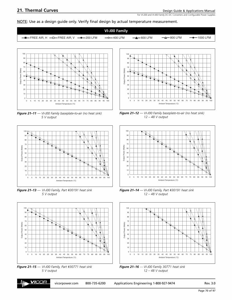
Design Guide & Applications ManualFor VI-200 and VI-J00 Family DC-DC Converters and Configurable Power Supplies
vicorpower.com 800-735-6200 Applications Engineering 1-800-927-9474 Rev. 3.0
Page 70 of 97
0
10
20
30
40
50
60
70
80
90
100
0 5 10 15 20 25 30 35 40 45 50 55 60 65 70 75 80 85 90 95 100
Ambient Temperature (°C)
Out
put P
ower
(W
atts
)
0
10
20
30
40
50
60
70
80
90
100
0 5 10 15 20 25 30 35 40 45 50 55 60 65 70 75 80 85 90 95 100
Ambient Temperature (°C)
Out
put P
ower
(W
atts
)
0
10
20
30
40
50
60
70
80
90
100
0 5 10 15 20 25 30 35 40 45 50 55 60 65 70 75 80 85 90 95 100
Ambient Temperature (°C)
Out
put P
ower
(W
atts
)
0
10
20
30
40
50
60
70
80
90
100
0 5 10 15 20 25 30 35 40 45 50 55 60 65 70 75 80 85 90 95 100
Ambient Temperature (°C)
Out
put P
ower
(W
atts
)
0
10
20
30
40
50
60
70
80
90
100
0 5 10 15 20 25 30 35 40 45 50 55 60 65 70 75 80 85 90 95 100
Ambient Temperature (°C)
Out
put P
ower
(W
atts
)
0
10
20
30
40
50
60
70
80
90
100
0 5 10 15 20 25 30 35 40 45 50 55 60 65 70 75 80 85 90 95 100
Ambient Temperature (°C)
Out
put P
ower
(W
atts
)
FREE AIR, H FREE AIR, V 200 LFM 400 LFM 600 LFM 800 LFM 1000 LFM
21. Thermal Curves
Figure 21–11 — VI-J00 Family baseplate-to-air (no heat sink) 5 V output
Figure 21–12 — VI-J00 Family baseplate-to-air (no heat sink) 12 – 48 V output
Figure 21–13 — VI-J00 Family, Part #30191 heat sink5 V output
Figure 21–14 — VI-J00 Family, Part #30191 heat sink12 – 48 V output
Figure 21–15 — VI-J00 Family, Part #30771 heat sink5 V output
Figure 21–16 — VI-J00 Family 30771 heat sink12 – 48 V output
VI-J00 Family
NOTE: Use as a design guide only. Verify final design by actual temperature measurement.

Design Guide & Applications ManualFor VI-200 and VI-J00 Family DC-DC Converters and Configurable Power Supplies
vicorpower.com 800-735-6200 Applications Engineering 1-800-927-9474 Rev. 3.0
Page 71 of 97
21. Thermal Curves
FREE AIR, H FREE AIR, V 200 LFM 400 LFM 600 LFM 800 LFM 1000 LFM
0
10
20
30
40
50
60
70
80
90
100
0 5 10 15 20 25 30 35 40 45 50 55 60 65 70 75 80 85 90 95 100
Ambient Temperature (°C)
Out
put P
ower
(W
atts
)
0
10
20
30
40
50
60
70
80
90
100
0 5 10 15 20 25 30 35 40 45 50 55 60 65 70 75 80 85 90 95 100
Ambient Temperature (°C)
Out
put P
ower
(W
atts
)
Figure 21–17 — VI-J00 Family, Part #30140 heat sink5 V output
Figure 21–18 — VI-200 Family, Part #30140 heat sink12 – 48 V output
VI-J00 Family
NOTE: Use as a design guide only. Verify final design by actual temperature measurement.
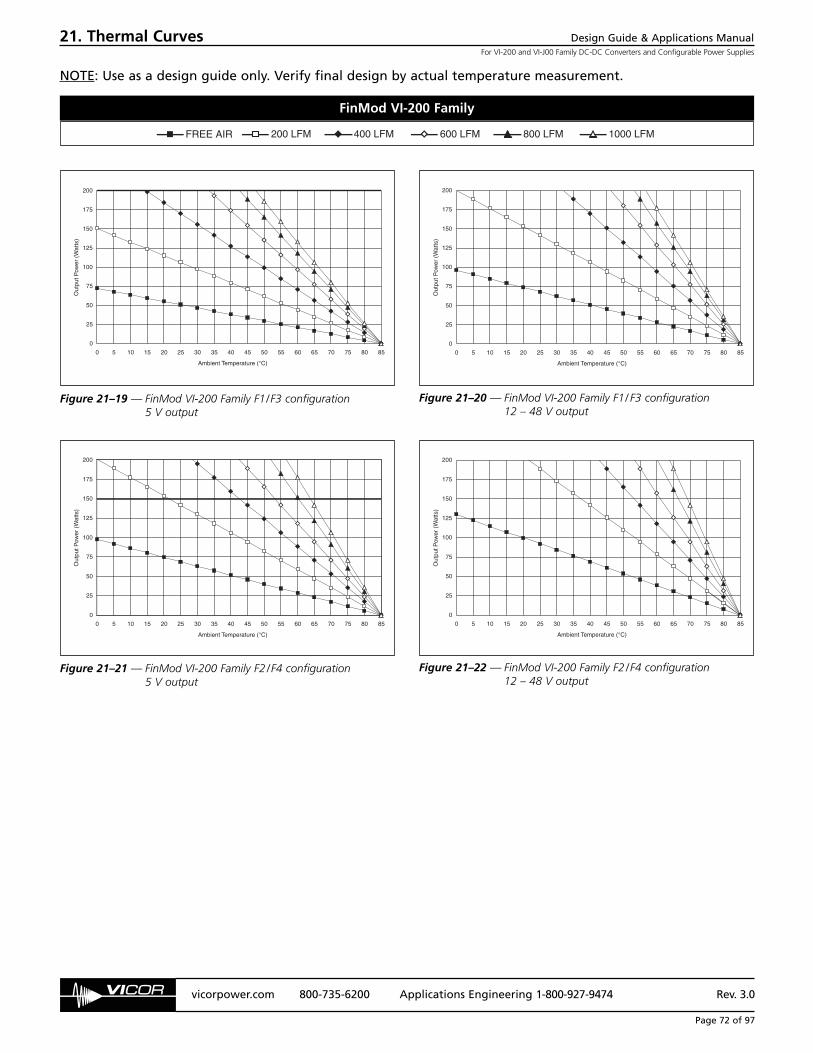
Design Guide & Applications ManualFor VI-200 and VI-J00 Family DC-DC Converters and Configurable Power Supplies
vicorpower.com 800-735-6200 Applications Engineering 1-800-927-9474 Rev. 3.0
Page 72 of 97
FREE AIR 200 LFM 400 LFM 600 LFM 800 LFM 1000 LFM
0
25
50
75
100
125
150
175
200
0 5 10 15 20 25 30 35 40 45 50 55 60 65 70 75 80 85
Ambient Temperature (°C)
Out
put P
ower
(W
atts
)
0
25
50
75
100
125
150
175
200
0 5 10 15 20 25 30 35 40 45 50 55 60 65 70 75 80 85
Ambient Temperature (°C)
Out
put P
ower
(W
atts
)
21. Thermal Curves
Figure 21–19 — FinMod VI-200 Family F1/F3 configuration 5 V output
Figure 21–20 — FinMod VI-200 Family F1/ F3 configuration12 – 48 V output
0
25
50
75
100
125
150
175
200
0 5 10 15 20 25 30 35 40 45 50 55 60 65 70 75 80 85
Ambient Temperature (°C)
Out
put P
ower
(W
atts
)
0
25
50
75
100
125
150
175
200
0 5 10 15 20 25 30 35 40 45 50 55 60 65 70 75 80 85
Ambient Temperature (°C)
Out
put P
ower
(W
atts
)
Figure 21–21 — FinMod VI-200 Family F2/F4 configuration 5 V output
Figure 21–22 — FinMod VI-200 Family F2/F4 configuration 12 – 48 V output
FinMod VI-200 Family
NOTE: Use as a design guide only. Verify final design by actual temperature measurement.

Design Guide & Applications ManualFor VI-200 and VI-J00 Family DC-DC Converters and Configurable Power Supplies
vicorpower.com 800-735-6200 Applications Engineering 1-800-927-9474 Rev. 3.0
Page 73 of 97
FREE AIR, H FREE AIR, V 200 LFM 400 LFM 600 LFM 800 LFM 1000 LFM
21. Thermal Curves
0
10
20
30
40
50
60
70
80
90
100
0 5 10 15 20 25 30 35 40 45 50 55 60 65 70 75 80 85 90 95 100
Ambient Temperature (°C)
Out
put P
ower
(W
atts
)
0
10
20
30
40
50
60
70
80
90
100
0 5 10 15 20 25 30 35 40 45 50 55 60 65 70 75 80 85 90 95 100
Ambient Temperature (°C)
Out
put P
ower
(W
atts
)
Figure 21–23 — FinMod VI-J00 Family F1/ F3 configuration 5 V output
Figure 21–24 — FinMod VI-J00 Family F1/ F3 configuration 12 – 48 V output
0
10
20
30
40
50
60
70
80
90
100
0 5 10 15 20 25 30 35 40 45 50 55 60 65 70 75 80 85 90 95 100
Ambient Temperature (°C)
Out
put P
ower
(W
atts
)
0
10
20
30
40
50
60
70
80
90
100
0 5 10 15 20 25 30 35 40 45 50 55 60 65 70 75 80 85 90 95 100
Ambient Temperature (°C)
Out
put P
ower
(W
atts
)
Figure 21–25 — FinMod VI-J00 Family F2/ F4 configuration 5 V output
Figure 21–26 — FinMod VI-J00 Family F2/F4 configuration 12 – 48 V output
FinMod VI-J00 Family
NOTE: Use as a design guide only. Verify final design by actual temperature measurement.

Design Guide & Applications ManualFor VI-200 and VI-J00 Family DC-DC Converters and Configurable Power Supplies
vicorpower.com 800-735-6200 Applications Engineering 1-800-927-9474 Rev. 3.0
Page 74 of 97
0
10
20
30
40
50
60
70
80
90
100
0 5 10 15 20 25 30 35 40 45 50 55 60 65 70 75 80 85 90 95 100
Ambient Temperature (°C)
Out
put P
ower
(W
atts
)
0
10
20
30
40
50
60
70
80
90
100
0 5 10 15 20 25 30 35 40 45 50 55 60 65 70 75 80 85 90 95 100
Ambient Temperature (°C)
Out
put P
ower
(W
atts
)
0
25
50
75
100
125
150
175
200
0 5 10 15 20 25 30 35 40 45 50 55 60 65 70 75 80 85
Ambient Temperature (°C)
Out
put P
ower
(W
atts
)
0
25
50
75
100
125
150
175
200
0 5 10 15 20 25 30 35 40 45 50 55 60 65 70 75 80 85
Ambient Temperature (°C)
Out
put P
ower
(W
atts
)
21. Thermal Curves
FREE AIR 200 LFM 400 LFM 600 LFM 800 LFM 1000 LFM
Figure 21–27 — SlimMod VI-200 Family 5 V output
Figure 21–28 — SlimMod VI-200 Family 12 – 48 V output
FREE AIR, H FREE AIR, V 200 LFM 400 LFM 600 LFM 800 LFM 1000 LFM
Figure 21–29 — SlimMod VI-J00 Family 5 V output
Figure 21–30 — SlimMod VI-J00 Family 12 – 48 V output
SlimMod VI-200 Family
SlimMod VI-J00 Family
NOTE: Use as a design guide only. Verify final design by actual temperature measurement.

Design Guide & Applications ManualFor VI-200 and VI-J00 Family DC-DC Converters and Configurable Power Supplies
vicorpower.com 800-735-6200 Applications Engineering 1-800-927-9474 Rev. 3.0
Page 75 of 97
0
25
50
75
100
125
150
175
200
0 5 10 15 20 25 30 35 40 45 50 55 60 65 70 75 80 85
Ambient Temperature (°C)
Out
put P
ower
(W
atts
)
0
25
50
75
100
125
150
175
200
0 5 10 15 20 25 30 35 40 45 50 55 60 65 70 75 80 85
Ambient Temperature (°C)
Out
put P
ower
(W
atts
)
21. Thermal Curves
Figure 21–31 — 1-Up ComPAC5 V output
Figure 21–32 — 1-Up ComPAC12 – 48 V output
FREE AIR, H FREE AIR, V 200 LFM 400 LFM 600 LFM 800 LFM 1000 LFM
0
50
100
150
200
250
300
350
400
0 5 10 15 20 25 30 35 40 45 50 55 60 65 70 75 80 85
Ambient Temperature (°C)
Out
put P
ower
(W
atts
)
0
50
100
150
200
250
300
350
400
0 5 10 15 20 25 30 35 40 45 50 55 60 65 70 75 80 85
Ambient Temperature (°C)
Out
put P
ower
(W
atts
)
Figure 21–33 — 2-Up ComPAC5 V output
Figure 21–34 — 2-Up ComPAC12 – 48 V output
0
75
150
225
300
375
450
525
600
0 5 10 15 20 25 30 35 40 45 50 55 60 65 70 75 80 85
Ambient Temperature (°C)
Out
put P
ower
(W
atts
)
0
75
150
225
300
375
450
525
600
0 5 10 15 20 25 30 35 40 45 50 55 60 65 70 75 80 85
Ambient Temperature (°C)
Out
put P
ower
(W
atts
)
Figure 21–35 — 3-Up ComPAC5 V output
Figure 21–36 — 3-Up ComPAC12 – 48 V output
ComPAC Family
NOTE: Use as a design guide only. Verify final design by actual temperature measurement.
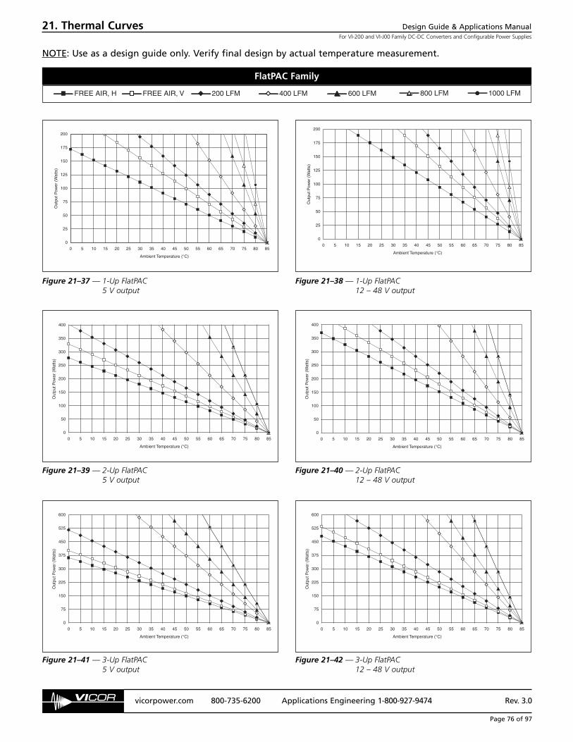
Design Guide & Applications ManualFor VI-200 and VI-J00 Family DC-DC Converters and Configurable Power Supplies
vicorpower.com 800-735-6200 Applications Engineering 1-800-927-9474 Rev. 3.0
Page 76 of 97
0
75
150
225
300
375
450
525
600
0 5 10 15 20 25 30 35 40 45 50 55 60 65 70 75 80 85
Ambient Temperature (°C)
Out
put P
ower
(W
atts
)
0
75
150
225
300
375
450
525
600
0 5 10 15 20 25 30 35 40 45 50 55 60 65 70 75 80 85
Ambient Temperature (°C)
Out
put P
ower
(W
atts
)
0
50
100
150
200
250
300
350
400
0 5 10 15 20 25 30 35 40 45 50 55 60 65 70 75 80 85
Ambient Temperature (°C)
Out
put P
ower
(W
atts
)
0
50
100
150
200
250
300
350
400
0 5 10 15 20 25 30 35 40 45 50 55 60 65 70 75 80 85
Ambient Temperature (°C)
Out
put P
ower
(W
atts
)
0
25
50
75
100
125
150
175
200
0 5 10 15 20 25 30 35 40 45 50 55 60 65 70 75 80 85
Ambient Temperature (°C)
Out
put P
ower
(W
atts
)
0
25
50
75
100
125
150
175
200
0 5 10 15 20 25 30 35 40 45 50 55 60 65 70 75 80 85
Ambient Temperature (°C)
Out
put P
ower
(W
atts
)
21. Thermal Curves
Figure 21–37 — 1-Up FlatPAC5 V output
Figure 21–38 — 1-Up FlatPAC12 – 48 V output
Figure 21–39 — 2-Up FlatPAC5 V output
Figure 21–40 — 2-Up FlatPAC12 – 48 V output
Figure 21–41 — 3-Up FlatPAC5 V output
Figure 21–42 — 3-Up FlatPAC12 – 48 V output
FREE AIR, H FREE AIR, V 200 LFM 400 LFM 600 LFM 800 LFM 1000 LFM
FlatPAC Family
NOTE: Use as a design guide only. Verify final design by actual temperature measurement.

Design Guide & Applications ManualFor VI-200 and VI-J00 Family DC-DC Converters and Configurable Power Supplies
vicorpower.com 800-735-6200 Applications Engineering 1-800-927-9474 Rev. 3.0
Page 77 of 97
21. Thermal Curves
0
24
48
72
96
120
144
168
192
216
240
264
0 5 10 15 20 25 30 35 40 45 50 55 60 65 70 75 80 85
Ambient Temperature (°C)
Out
put P
ower
(Wat
ts)
0
100
200
300
400
500
600
0 5 10 15 20 25 30 35 40 45 50 55 60 65 70 75 80 85
Ambient Temperature (°C)
Out
put P
ower
(Wat
ts)
0
50
100
150
200
250
300
350
400
0 5 10 15 20 25 30 35 40 45 50 55 60 65 70 75 80 85
Ambient Temperature (°C)
Out
put P
ower
(Wat
ts)
Figure 21–43 — Output power derating vs. temperature, Vout ≥ 12 V Figure 21–44 — Output power derating vs. temperature, Vout = 5 V
Figure 21–45 — Output power derating vs. temperature, Vout = 3.3 V
FREE AIR 200 LFM 400 LFM 600 LFM 800 LFM 1000 LFM
PFC FlatPAC Family
NOTE: Use as a design guide only. Verify final design by actual temperature measurement.

Design Guide & Applications ManualFor VI-200 and VI-J00 Family DC-DC Converters and Configurable Power Supplies
vicorpower.com 800-735-6200 Applications Engineering 1-800-927-9474 Rev. 3.0
Page 78 of 97
22. Recommended Soldering Methods, Lead Free Pins (RoHS)
The following chapters contain soldering information forthe following Vicor product families; Maxi, Mini, Micro; VE-200, VE-J00; VI BRICK, and similar package filters andfront-ends. This document is intended to provide guidancefor making high-quality solder connections of RoHS-compliant Vicor power modules to printed circuit boards.This application note applies to lead-free soldering ofVicor’s RoHS- compliant modules. The following providesan outline for appropriate soldering procedures and theevaluation of solder joints to ensure an optimalconnection to the power module. Common solderingdefects will be examined and direction will be provided fordetecting and handling them. Vicor’s manufacturingfacilities use the IPC-A-610 standards for establishingquality solder joints. It is recommended thatmanufacturing processes using Vicor modules refer tothese same standards, which can be found, along withsupporting documentation, at www.ipc.org.
ANALYSIS OF A GOOD SOLDER JOINT
The IPC-A-610 standard requires that solder fill at least75% of the barrel to ensure a solid connection. Ideally, allconnections should have a 100% fill. To accomplish this,the solder applied to both the barrel and the pin mustexhibit a process known as wetting. Wetting occurs whenliquid solder on a surface is heated to the point that itloses a significant amount of latent surface tension andevenly coats the surface via capillary action (both cohesionand adhesion).
During the soldering process wetting can be identified byan even coating of solder on the barrel and pin. Inaddition, coating the surface of barrel and pin, the solderwill gather at the intersection of the two and produce atrailing fillet along each surface. Once wetting has occurred,then upon solidification it will bond appropriately to bothcomponents, producing a quality connection.
Figure 22–1 shows a side profile of a good solder jointwith a power module. Notice that the solder forms aconcave meniscus between pin and barrel. This is anexample of a properly formed fillet and is evidence ofgood wetting during the soldering process. The jointbetween solder and pin as well as solder and pad shouldalways exhibit a feathered edge. In Figure 22–1 it can alsobe seen that the solder covers a good deal of the surfacearea of both the pin and the pad. This is also evidence ofgood wetting. (Notice also that the solder joint is dullcompared to leaded processing). This is evidence of goodimmobilization of the joint during cooling as well as goodcleaning of the board prior to soldering. All solderingconnections should exhibit similar characteristics
regardless of whether they are soldered by hand, byfountain, or by wave.
In examining a solder joint, be sure that there is no solderconnecting one pad to another. This is known as a solderbridge and will be discussed later.
SOLDERING PROCEDURES
Hand Soldering. Before soldering, make sure that thePCB is clean and free of debris, chemical residue, or liquid.It is not recommended that additional flux other thanwhat is contained in the solder be used during solderingbecause it potentially leaves a residue that cannot beremoved without potentially damaging or compromisingthe power module. Also, the presence of these residueson the modules may cause harm or improper operation.
The pins on Vicor modules are optimized to provide a low-resistance electrical connection. The final mountingscheme for any module should be designed to minimizeany potential mechanical stress on the pins and solderjoints. Modules with heat sinks or modules used insystems that are subject to shock or vibration should usestandoffs to minimize stress on the pins. It is notrecommended that discrete wires or connectors besoldered directly onto a module.
Also necessary for a good solder connection is pin protrusionfrom the PCB. It is not possible to create a good solderjoint without some protrusion of module pins from thePCB. If the PCB is too thick to allow good pin protrusion,consider using Vicor module accessories such as sockets toallow proper mounting. Before soldering, the moduleshould be mechanically affixed or immobilized with
Figure 22–1 — Side profile of Maxi or Mini module’s RoHS solder joint.
OVERVIEW

Design Guide & Applications ManualFor VI-200 and VI-J00 Family DC-DC Converters and Configurable Power Supplies
vicorpower.com 800-735-6200 Applications Engineering 1-800-927-9474 Rev. 3.0
Page 79 of 97
22. Recommended Soldering Methods, Lead Free Pins (RoHS)
respect to the PCB to ensure no movement during thesoldering process. The standoffs can be used for thisprocess. Vicor power modules contain two types of pins:power pins (which deliver the power to the load and aretypically sized according to the rated output current) andsignal pins (which typically carry very little current and areof a uniform size across a given product family). The largerthe pin, the more soldering time required to form anadequate connection. In addition to the sizing of the pin,the time required to create a robust connection will varydepending on several parameters:
1. PCB Thickness. The thicker the printed circuit board, the more heat it is able to dissipate, and will require more soldering time.
2. Copper Trace Area. Power pins require large copper traces to minimize resistive power losses in carrying thepower to the load. Since the copper tends to conductheat well, the actual sizes of these copper tracesdirectly affect the amount of time necessary to heatthe PCB socket.
3. Copper Trace Thickness. As above, the thickness of thecopper trace is a function of output current of themodule, and has a direct impact on the amount ofsoldering time. Typically, PCB copper thickness isspecified in terms of weight per square foot, typically 2 oz. or 3 oz. copper for current-carrying planes.
4. Soldering Iron Power. A higher power soldering iron can source more heat and thus take less time to heat a PCB trace. As a soldering iron is heating a point on the board, everything that is adjacent to this point is beingheated as well, including the Vicor power module. A large copper trace, because it conducts heat very well, will exhibit less of a thermal gradient, and thus a low-power soldering iron will have to heat the whole trace to a higher temperature before the area close to the iron is hot enough to flow solder. Because the trace and board are both dissipating and conducting thermal energy, some irons may not have enough power to heat a trace to the temperature that will allow proper soldering.
5. Tip Temperature. Typical SAC-type solder melts at 419 – 491°F (215 – 225°C). Pb-free soldering requires a tip temperature of about 800°F. A higher tip temperature will bring the barrel and pin above the melting point of solder faster. However, a higher tip temperature may cause damage to the pad, printed circuit board, or module pin.
6. Type of Lead-free Solder. The actual melting point ofthe solder varies depending on the type of solder used and affects the necessary temperature of the pad and pin for flow. Vicor recommends SAC305 SnAgCu solder for use on Vicor power modules.
7. Tip Size. A larger tip will be able to heat a larger surface area, thus lowering soldering time.
Since there are so many factors that influence solderingtime, listing actual times is difficult. In general, it isrecommended that the joint be examined post-process toinsure a quality soldering joint. If necessary, differentparameters can then be varied in order to ensure a solidprocess. The soldering times listed in Table 22–1 can beused as a guideline for establishing more application andprocess specific parameters. Below are some recommen-dations for general practice:
1. Do not run tip temperature above 810°F (430°C). This will greatly increase the risk of damaging the pads, traces, printed circuit board, or Vicor power module. Check with the printed circuit board manufacturer thatthe boards are RoHS capable and for any additional recommendations in regard to temperature.
2. Apply the soldering iron to one side of the pin and padand apply the solder to the other, allowing the heatfrom the pin and pad to melt the solder. Do not apply solder to the soldering iron and subsequently attempt to transfer it to the pad and pin. Melting the solder by applying it directly to the soldering iron does not guarantee adequate wetting on the joint and is not considered good technique.
3. Do not apply excessive pressure with the soldering iron to the printed circuit board, barrel, or pad. This couldresult in breaking a trace, dislodging a barrel, or damaging the PCB, which becomes noticeably softerwhen heated.
4. Do not apply the soldering iron to a connection for an extended period of time or damage to the module could result. If the soldering times exceed the upper limit listed in Table 22–1, consider using a larger tip or a higher power soldering iron.
5. Make sure PCB pads and holes are clean before to soldering.
6. Solders with no-clean flux may be used to facilitatesoldering.
7. Keep the tip of the soldering iron clean and free from resin. Apply a small amount of solder directly to the tip of the iron. This process is known as tinning.

Design Guide & Applications ManualFor VI-200 and VI-J00 Family DC-DC Converters and Configurable Power Supplies
vicorpower.com 800-735-6200 Applications Engineering 1-800-927-9474 Rev. 3.0
Page 80 of 97
22. Recommended Soldering Methods, Lead Free Pins (RoHS)
8. Be careful not to jar the module or PCB while the solder is cooling. This could result in a cold solder joint, a void in the barrel, or a cracked joint.
9. If it is necessary to re-solder a joint, remove all existingsolder from the pad and pin before reapplying solder.
10. Use of a soldering gun is not recommended for soldering Vicor modules.
11. It is not recommended that Maxi / Mini / Micro modulepins be trimmed under any circumstances.
As a procedural benchmark, given an 800°F (427ºC)temperature on a 60 W iron with a 3 mm tip, approximatetimes to solder a Vicor power module to a 0.062 (1,5 mm)thick PCB board with an appropriately sized copper tracewould be in the range of Table 22–1.
Again, please note that soldering for significantly longerperiods of time than those listed above could result indamage to the module. Table 22–1 should not be usedwithout verifying that the times will produce a qualitysoldering joint as defined in the previous sections.
Wave Soldering. Vicor modules achieve an adequatesolder connection on a wave-soldering machine withconveyor speeds from three to seven feet per minute. Aswith hand soldering, times and parameters vary with theproperties of the PCB and copper traces. As a standardbenchmark, the parameters below may be used. As withhand-soldered boards, the results should be examined toensure a quality soldering joint and a sound process.
Wave Soldering Profile.
1. Bottom-side preheaters: Zone 1: 350°F (177°C),Zone 2: 300°F (149°C), Zone 3: 675°F (357°C)
2. Top-side preheaters: 220 – 235°F (104 – 113°C)
3. Wave temperature: 510°F (266°C)
4. Wave type: 4.25 in (107,95 mm) standard laminar wave
Preheating of the PCB is generally required for wavesoldering operations to ensure adequate wetting of thesolder to the PCB. The recommended temperature for PCBtopside is 203 – 248°F (95 – 120°C) prior to the moltenwave. Thick, multilayer PCBs should be heated toward theupper limit of this range, while simple two-layer PCBsshould be heated to the lower limit. These parameters areconsistent with generally accepted requirements forcircuit-card assembly. The power module is often muchmore massive than other components mounted to thePCB. During wave solder preheating, the pins willdissipate much of their absorbed heat within the module;therefore, adjustments to preheaters alone will notimprove module soldering significantly. A more effectiveway to improve the soldering of the module is to lowerthe conveyor speed and increase the dwell time in the moltenwave. Approximately 5 seconds of exposure to the moltenwave is required to achieve an acceptable solder joint fora Maxi / Mini / Micro power module. The VE-200 / VE-J00/VE-HAM and VI BRICK modules should solder inapproximately 4 seconds of molten wave exposure.
Post Solder Cleaning. Vicor modules are not hermeticallysealed and must not be exposed to liquid, including butnot limited to cleaning solvents, aqueous washingsolutions or pressurized sprays. Cleaning the backside ofthe PCB is acceptable provided no solvent contacts thebody of the module.
When soldering, it is recommended that no-clean fluxsolder be used, as this will ensure that potentiallycorrosive mobile ions will not remain on, around, or under the module following the soldering process.
If the application requires the PCB to be subject to anaqueous wash after soldering, then it is recommendedthat Vicor module accessories such as through-hole orsurface-mount sockets be used. These sockets should bemounted to the PCB, and the modules subsequentlyinserted following the aqueous washing sequence.
De-soldering Vicor Modules. Vicor modules should notbe re-used after desoldering for the following reasons:
1. Most de-soldering procedures introduce damaging mechanical and thermal stresses to the module.
2. Devices or processes that may be capable of desoldering a Vicor module from a printed-circuit board without causing damage have not been qualified for use with Vicor modules.
For applications that require removal of a module with theintent of reuse, use Vicor socketing systems.
Table 22–1 — Recommended pin soldering times for RoHSfamily modules
Converter Family Pin Type Soldering Time (range)
VE-200 / VE-J00 Signal 3 – 5 secondsVE-200 Power 5 – 8 secondsVE-J00 Power 4 – 7 secondsMaxi / Mini / Micro Signal 3 – 5 secondsMaxi Power 5 – 8 secondsMini Power 4 – 7 secondsMicro Power 3 – 5 secondsVI BRICK Input & Signal 3 – 5 secondsVI BRICK Power 4 – 7 secondsAlso relevant for similar packaged accessory modules

Design Guide & Applications ManualFor VI-200 and VI-J00 Family DC-DC Converters and Configurable Power Supplies
vicorpower.com 800-735-6200 Applications Engineering 1-800-927-9474 Rev. 3.0
Page 81 of 97
22. Recommended Soldering Methods, Lead Free Pins (RoHS)
Index of Common Soldering defects.
1. Solder Bridge. A short circuit between two electricallyinadvertently forming a “bridge” or connection betweenthe two points.
Recommended Solution. Use a smaller soldering tip, or hold the tip at a different angle when soldering, so as to contact only one pad at a time.
2. Cold Solder. An incomplete or poor connection caused by either the barrel or the pin not being heated to the flow temperature of solder. A cold solder joint will typically exhibit a convex meniscus with possibly a dark spot around the barrel or pad. Also, a cold solder joint will not be shiny, but will typically have a “dirty” appearance.
CAUTION: A cold solder joint is not necessarily an open connection electrically, and cannot be diagnosed by a simple continuity check. A cold solder joint is frequently an electrically inter-mittent connection and is best diagnosed by way of visual inspection. A cold solder joint will likely become electrically open following a period of temperature cycling.
Recommended Solution. Increase soldering iron temperature, soldering time, or use a soldering iron with a higher output wattage if hand soldering. If wave soldering, lower conveyor speed or increase preheat temperature.
3. PC Board Damage. An intermittent or poor connectioncaused by damage to a trace, pad, or barrel. A damagedpad is best identified by a burn mark on the PCB, or a trace pad that moves when prodded with a mechanical object.
Recommended Solution. Lower the soldering iron temperature or the soldering time. If damage persists, use a lower power iron, or consult with the manufacturerof the PCB for recommended soldering guidelines.
4. De-wetting. The solder initially appears to wet but then pulls back to expose the pad surface. More common in wave-soldering.
Recommended Solution. Make sure the PCB is clean prior to soldering.
5. Dry Joint. The solder has a dull gray appearance as opposed to a bright silver surface. The solder joint mayhave a mottled look as well, with jagged ridges. It is caused by the solder joint moving before it has completely cooled.
Recommended Solution. Immobilize the module with respect to the PCB to ensure that the solder joint cools properly.
6. Icicles. Jagged or conical extensions from solder fillet. These are caused by soldering with the temperature toolow, or soldering to a highly heat absorbent surface.
Recommended Solution. Increase the soldering temperature, but not outside the recommended limits. If necessary, use a higher power soldering iron.
7. Pinholes. Small or large holes in surface of solder joint, most commonly occurring in wave solder systems.
Recommended Solution. Increase preheat or topside heater temperature, but not outside the recommended limits.
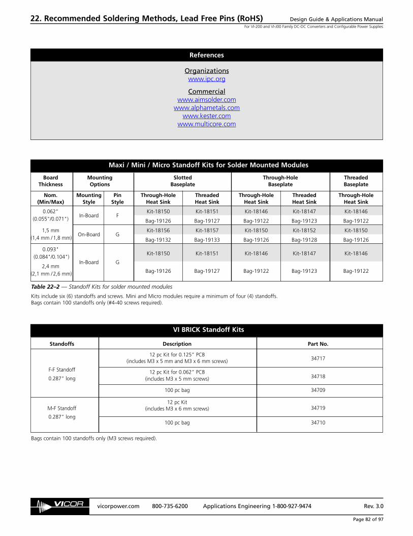
Design Guide & Applications ManualFor VI-200 and VI-J00 Family DC-DC Converters and Configurable Power Supplies
vicorpower.com 800-735-6200 Applications Engineering 1-800-927-9474 Rev. 3.0
Page 82 of 97
22. Recommended Soldering Methods, Lead Free Pins (RoHS)
Organizationswww.ipc.org
Commercialwww.aimsolder.com
www.alphametals.comwww.kester.com
www.multicore.com
References
Maxi / Mini / Micro Standoff Kits for Solder Mounted Modules
Board Mounting Slotted Through-Hole ThreadedThickness Options Baseplate Baseplate Baseplate
Nom. Mounting Pin Through-Hole Threaded Through-Hole Threaded Through-Hole(Min/Max) Style Style Heat Sink Heat Sink Heat Sink Heat Sink Heat Sink
0.062"In-Board F
Kit-18150 Kit-18151 Kit-18146 Kit-18147 Kit-18146(0.055"/0.071") Bag-19126 Bag-19127 Bag-19122 Bag-19123 Bag-19122
1,5 mmOn-Board G
Kit-18156 Kit-18157 Kit-18150 Kit-18152 Kit-18150(1,4 mm /1,8 mm) Bag-19132 Bag-19133 Bag-19126 Bag-19128 Bag-19126
0.093"(0.084"/0.104")
In-Board G
Kit-18150 Kit-18151 Kit-18146 Kit-18147 Kit-18146
2,4 mmBag-19126 Bag-19127 Bag-19122 Bag-19123 Bag-19122(2,1 mm /2,6 mm)
Table 22–2 — Standoff Kits for solder mounted modules
Kits include six (6) standoffs and screws. Mini and Micro modules require a minimum of four (4) standoffs. Bags contain 100 standoffs only (#4-40 screws required).
Standoffs Description Part No.
12 pc Kit for 0.125” PCB(includes M3 x 5 mm and M3 x 6 mm screws) 34717
F-F Standoff 12 pc Kit for 0.062” PCB0.287” long (includes M3 x 5 mm screws) 34718
100 pc bag 34709
M-F Standoff12 pc Kit
0.287” long
(includes M3 x 6 mm screws) 34719
100 pc bag 34710
VI BRICK Standoff Kits
Bags contain 100 standoffs only (M3 screws required).

Design Guide & Applications ManualFor VI-200 and VI-J00 Family DC-DC Converters and Configurable Power Supplies
vicorpower.com 800-735-6200 Applications Engineering 1-800-927-9474 Rev. 3.0
Page 83 of 97
23. Recommended Soldering Methods,Tin Lead Pins, and InMate Sockets
The following chapters contain soldering information forthe following Vicor product families; Maxi, Mini, Micro; VI-200, VI-J00; VI BRICK, and similar package filters andfront-ends. This document is intended to provide guidancein utilizing soldering practices to make high-qualityconnections of Vicor power modules to printed circuitboards. Some care will be taken to outline appropriatesoldering procedures as well as the evaluation of solderjoints in a manner that enables the customer to ensurethat the end application has an optimal connection to thepower module. Common soldering defects will beexamined and direction will be provided for detecting andhandling the common defects.
Vicor’s manufacturing facilities use the IPC-A-610Cstandards as a means of establishing quality solder joints.It is recommended that manufacturing processes usingVicor modules refer to these same standards, which canbe found, along with supporting documentation, atwww.ipc.org.
ANALYSIS OF A GOOD SOLDER JOINT
The IPC-A-610C standard requires that solder fill at least75% of the barrel in order to ensure a solid connection.Ideally, all connections should have a 100% fill. In order toaccomplish this, the solder applied to both the barrel andthe pin must exhibit a process known as wetting. Wettingoccurs when liquid solder on a surface is heated to thepoint that it loses a significant amount of latent surfacetension and evenly coats the surface via capillary action(both cohesion and adhesion).
During the soldering process wetting can be identified byan even coating of solder on the barrel and pin. Inaddition to coating the surface of barrel and pin, thesolder will gather at the intersection of the two andproduce a trailing fillet along each surface. Once wettinghas occurred, then upon solidification it will bondappropriately to both components, producing a qualityconnection. Figure 23–1 shows a side profile of a goodsolder joint with a Mini power module. Notice that forboth examples the solder forms a concave meniscusbetween pin and barrel. This is an example of a properlyformed fillet and is evidence of good wetting during thesoldering process. The joint between solder and pin aswell as solder and pad should always exhibit a featherededge. In Figure 23–1 it can also be seen that the soldercovers a good deal of the surface area of both the pinand the pad. This is also evidence of good wetting. Noticealso that the solder joint has a smooth surface with asilver color. This is evidence of good immobilization of thejoint during cooling as well as good cleaning of the boardprior to soldering. All soldering connections should exhibit
similar characteristics regardless of whether they aresoldered by hand or wave soldered.
Figure 23–2 is a top view of the signal and power pin of aMaxi or Mini module properly soldered to a printed circuitboard. Notice that both the joint and the area around thejoint are clean and free from resin and solder residue. Alsothe pad and printed circuit board adjacent to the barrelare not burnt or discolored and are solidly attached toeach other. In examining a solder joint, be sure that thereis no solder connecting one pad to another. This is knownas a solder bridge and will be discussed further along withother potential soldering defects.
Figure 23–2 — Maxi / Mini output power pin and Sense pin
Figure 23–1 — Side profile of a Mini module solder joint
OVERVIEW

Design Guide & Applications ManualFor VI-200 and VI-J00 Family DC-DC Converters and Configurable Power Supplies
vicorpower.com 800-735-6200 Applications Engineering 1-800-927-9474 Rev. 3.0
Page 84 of 97
23. Recommended Soldering Methods,Tin Lead Pins, and InMate Sockets
Hand Soldering. Before soldering, make sure that thePCB is clean and free of debris, chemical residue, or liquid.It is not recommended that additional flux other thanwhat is contained in the solder be used during solderingas it potentially leaves a residue that cannot be removedwithout potentially damaging or compromising the powermodule. Also, the presence of these residues themselveson the modules may cause harm or improper operation. The pins on Vicor modules are optimized in design forproviding a low-resistance electrical connection. The finalmounting scheme for any module should be designed soas to minimize any potential mechanical stress on the pinsand solder joints. Modules with heat sinks or modules usedin systems that are subject to shock or vibration shoulduse standoffs to minimize stress on the pins. Tin / leadpins are specifically designed for soldering applicationswhile gold pin options are specified for socketedapplications (see SurfMate or InMate mounting systems).It is not recommended that discrete wires or connectorsbe soldered directly onto a module.
Also necessary for a good solder connection is pinprotrusion from the PCB. It is not possible to create agood solder joint without some protrusion of module pinsfrom the PCB. If the PCB is too thick to allow good pinprotrusion, consider using Vicor module accessories suchas sockets to allow proper mounting.
Before soldering, the module should be mechanicallyaffixed or immobilized with respect to the PCB to ensureno movement during the soldering process. The standoffscan be used for this process.
Vicor power modules contain two types of pins: powerpins (which deliver the power to the load and are typicallysized according to the rated output current) and signalpins (which typically carry very little current and are of auniform size across a given product family). The larger thepin, the more soldering time required to form anadequate connection. In addition to the sizing of the pinthe time required to create a robust connection will varydepending on several parameters:
1. PCB Thickness. The thicker the printed circuit board is,the more heat it is able to dissipate, and thus it willrequire more soldering time.
2. Copper Trace Area. Power pins require large coppertraces to minimize resistive power losses in carrying the power to the load. Since the copper tends toconduct heat rather well, the actual size of these copper traces directly affect the amount of timenecessary to heat the PCB socket.
3. Copper Trace Thickness. As above, the thickness of the copper trace is a function of output current of themodule, and has a direct impact on the amount ofsoldering time. Typically, PCB copper thickness is specified in terms of weight per square foot, typically2 oz. or 3 oz. copper for current-carrying planes.
4. Soldering Iron Power. A higher power soldering ironcan source more heat and thus take less time to heat a PCB trace. When a soldering iron is heating a pointon the board, everything that is adjacent to this pointis being heated as well, including the Vicor powermodule. A large copper trace, because it conductsheat very well, will exhibit less of a thermal gradientand thus a low-power soldering iron will have to heatthe whole trace to a higher temperature before thearea close to the iron is hot enough to flow solder.Because the trace and board are both dissipating andconducting thermal energy, some irons may not haveenough power to heat a trace to the temperature thatwill allow proper soldering.
5. Tip Temperature. Typical 63 / 37 solder melts at 392°F(200°C). A higher tip temperature will bring the barrel and pin above the melting point of solder faster. However, a higher tip temperature may cause damage to the pad, printed circuit board, or module pin.
6. Type of Solder. The actual melting point of the soldervaries depending on the type of solder used and affects the necessary temperature of the pad and pinfor flow. Vicor recommends 63 / 37 SnPb solder for use on Vicor power modules.
7. Tip Size. A larger tip will be able to heat a largersurface area, thus lowering soldering time.
SOLDERING PROCEDURES

Design Guide & Applications ManualFor VI-200 and VI-J00 Family DC-DC Converters and Configurable Power Supplies
vicorpower.com 800-735-6200 Applications Engineering 1-800-927-9474 Rev. 3.0
Page 85 of 97
23. Recommended Soldering Methods,Tin Lead Pins, and InMate Sockets
Since there are so many factors that influence solderingtime, listing actual times is difficult. In general, it is recommended that the joint be examined post-process toensure a quality soldering joint. If necessary, differentparameters can then be varied in order to ensure a solidprocess. The soldering times listed in Table 23–1 can beused as a guideline for establishing more application andprocess-specific parameters. Below are some recommen-dations for general practice:
1. Do not run tip temperature above 750°F (400°C)because it will greatly increase the risk of damagingthe pads, traces, printed circuit board, or Vicor powermodule. Check with the printed circuit boardmanufacturer for any additional recommendationswith regards to temperature.
2. Apply the soldering iron to one side of the pin andpad and apply the solder to the other, allowing theheat from the pin and pad to melt the solder. Do notapply solder to the soldering iron and subsequentlyattempt to transfer it to the pad and pin. Melting thesolder by applying it directly to the soldering iron doesnot guarantee adequate wetting on the joint and isnot considered good technique.
3. Do not apply excessive pressure with the solderingiron to the printed circuit board, barrel, or pad. Thiscould result in breaking a trace, dislodging a barrel ordamaging the PCB, which becomes noticeably softerwhen heated.
4. Do not apply the soldering iron to a connection for an extended period of time or damage to the module could result. If the soldering times exceed the upper limit listed in Table 23–1, consider using a larger tip ora higher power soldering iron.
5. Make sure PCB pads and holes are clean prior to soldering.
6. Solders with no-clean flux may be used to facilitatesoldering.
7. Keep the tip of the soldering iron clean and free fromresin. Apply a small amount of solder directly to the tip of the iron. This process is known as tinning.
8. Be careful not to jar the module or PCB while the solder is cooling. This could result in a cold solder joint, a void in the barrel, or a cracked joint.
9. If it is necessary to re-solder a joint, remove all existing solder from the pad and pin prior to reapplying solder.
10. Use of a soldering gun is not recommended forsoldering Vicor modules.
11. It is not recommended that Maxi, Mini, Micro module pins be trimmed under any circumstances.
12. The caps of the InMate socket are designed to repelsolder. It is normal for this surface to be free of solder.
As a procedural benchmark, given a 750°F (400°C)temperature on a 60 W iron with a 0.19 in (3 mm) tip,approximate times to solder a Vicor power module to a0.062 (1,5 mm) thick PCB board with an appropriatelysized copper trace would be in the range of Table 14–1.
Again, please note that soldering for significantly longerperiods of time than the time listed above could result indamage to the module. The time listed in Table 23–1 shouldnot be used without verifying that the times will producea quality soldering joint as defined in the previous sections.
Wave Soldering. Vicor modules achieve an adequatesolder connection on a wave soldering machine withconveyor speeds from three to seven feet per minute. Aswith hand soldering, times and parameters vary with theproperties of the PCB and copper traces. As a standardbenchmark the parameters below may be used. As withhand-soldered boards, the results should be examined toensure a quality soldering joint and a sound process.
Wave Soldering Profile.
1. Bottom-side preheaters: Zone 1: 650°F (343°C),Zone 2: 750°F ( 398°C)
2. Top-side preheaters: 203 – 248°F (95 – 120°C)
3. Wave temperature: 500°F (260°C)
4. Wave type: 4.25 in (107,9 mm) standard laminar wave
Preheating of the PCB is generally required for wavesoldering operations to ensure adequate wetting of thesolder to the PCB. The recommended temperature for PCBtopside is 203 – 248°F (95 – 120°C) prior to the moltenwave. Thick, multilayer PCBs should be heated toward theupper limit of this range, while simple two-layer PCBsshould be heated to the lower limit. These parameters areconsistent with generally accepted requirements forcircuit-card assembly.
Converter Family Pin Type Soldering Time (range)
VI-200 / VI-J00 Signal 3 – 5 secondsVI-200 Power 5 – 8 secondsVI-J00 Power 4 – 7 secondsMaxi / Mini / Micro Signal 3 – 5 secondsMaxi Power 5 – 8 secondsMini Power 4 – 7 secondsMicro Power 3 – 5 seconds
Table 23–1 — Recommended pin soldering times for Vicor modules
Design Guide & Applications ManualFor VI-200 and VI-J00 Family DC-DC Converters and Configurable Power Supplies
vicorpower.com 800-735-6200 Applications Engineering 1-800-927-9474 Rev. 3.0
Page 86 of 97
23. Recommended Soldering Methods,Tin Lead Pins, and InMate Sockets
The power module is often much more massive thanother components mounted to the PCB. During wavesolder preheating, the pins will dissipate much of theirabsorbed heat within the module. Adjustments topreheaters alone, therefore, will not improve modulesoldering significantly.
A more effective way to improve the soldering of the moduleis to lower the conveyor speed and increase the dwell timein the molten wave. Approximately 5 seconds of exposureto the molten wave is required to achieve an acceptablesolder joint for a Maxi, Mini, or Micro power module.
Post Solder Cleaning. Vicor modules are not hermeticallysealed and must not be exposed to liquid, including butnot limited to cleaning solvents, aqueous washingsolutions, or pressurized sprays. Cleaning the backside ofthe PCB is acceptable provided no solvent contacts thebody of the module.
When soldering, it is recommended that no-clean fluxsolder be used, as this will ensure that potentiallycorrosive mobile ions will not remain on, around, or underthe module following the soldering process.
If the application requires the PCB to be subject to anaqueous wash after soldering, then it is recommendedthat Vicor module accessories such as through-hole orsurface-mount sockets be used. These sockets should bemounted to the PCB and the modules subsequentlyinserted following the aqueous washing sequence.
De-soldering Vicor Modules. Vicor modules should notbe re-used after desoldering for the following reasons:
1. Most de-soldering procedures introduce damagingmechanical and thermal stresses to the module.
2. Devices or processes that may be capable of de-soldering a Vicor module from a printed circuit board without causing damage have not been qualified for use with Vicor modules. For applications that require removal of a module with the intent of reuse, use Vicor socketing systems.
Index of Common Soldering defects.
1. Solder Bridge. A short circuit between two electricallyunconnected points caused by a piece of solder inadvertently forming a “bridge” or connection between the two points.
Recommended Solution. Use a smaller soldering tip, or hold the tip at a different angle when soldering, so as to only contact one pad at a time.
2. Cold Solder. An incomplete or poor connection caused by either the barrel or the pin not being heated to the flow temperature of solder. A cold solder joint will typically exhibit a convex meniscus with possibly a dark spot around the barrel or pad. Also a cold solder joint will not be shiny, but will typically have a “dirty”appearance.
CAUTION: A cold solder joint is not necessarily an open connection electrically, and cannot be diagnosed by a simple continuity check. A cold solder joint is frequently an electrically intermit-tent connection and is best diagnosed by visual inspection. A cold solder joint will likely become electrically open following a period of temp-erature cycling.
Recommended Solution. Increase soldering iron temperature, soldering time, or use a soldering iron with a higher output wattage if hand soldering. If wave soldering, lower conveyor speed or increase preheat temperature.
3. PC Board Damage. An intermittent or poor connection caused by damage to a trace, pad, or barrel. A damaged pad is best identified by a burn mark on the PCB, or a trace of pad that moves when prodded with a mechanical object.
Recommended Solution. Lower the soldering iron temperature or the soldering time. If damage persists use a lower power iron, or consult with the manufacturerof the PCB for recommended soldering guidelines.
4. De-wetting. The solder initially appears to wet but then pulls back to expose the pad surface, more common in wave soldering.
Recommended Solution. Make sure the PCB is clean prior to soldering.

Design Guide & Applications ManualFor VI-200 and VI-J00 Family DC-DC Converters and Configurable Power Supplies
vicorpower.com 800-735-6200 Applications Engineering 1-800-927-9474 Rev. 3.0
Page 87 of 97
23. Recommended Soldering Methods,Tin Lead Pins, and InMate Sockets
5. Dry Joint. The solder has a dull gray appearance as opposed to a bright silver surface. The solder joint may have a mottled look as well, with jagged ridges. It is caused by the solder joint moving before completely cooled.
Recommended Solution. Immobilize the module with respect to the PCB to ensure that the solder jointcools properly.
6. Icicles. Jagged or conical extensions from solder fillet. These are caused by soldering with the temperature too low, or soldering to a highly heat-absorbent surface.
Recommended Solution. Increase the soldering temperature, but not outside the recommended limits. If necessary, use a higher power soldering iron.
7. Pinholes. Small or large holes in surface of solder joint, most commonly occurring in wave-solder systems.
Recommended Solution. Increase preheat or topside heater temperature, but not outside the recommended limits.
Organizationswww.ipc.org
Commercialwww.aimsolder.com
www.alphametals.comwww.kester.com
www.multicore.com
References
Maxi / Mini / Micro Standoff Kits for Solder Mounted Modules*
Board Mounting Slotted Through-Hole ThreadedThickness Options Baseplate Baseplate Baseplate
Nom. Mounting Pin Through-Hole Threaded Through-Hole Threaded Through-Hole(Min/Max) Style Style Heat Sink Heat Sink Heat Sink Heat Sink Heat Sink
0.062"In-Board Short Kit-18150 Kit-18151 Kit-18146 Kit-18147 Kit-18146
(0.055"/ 0.071") Tin/Lead Bag-19126 Bag-19127 Bag-19122 Bag-19123 Bag-19122
(1,5 mm)On-Board L
Kit-18156 Kit-18157 Kit-18150 Kit-18152 Kit-18150
(1,4 mm / 1,8 mm) Bag-19132 Bag-19133 Bag-19126 Bag-19128 Bag-19126
0.093" Kit-18150 Kit-18151 Kit-18146 Kit-18147 Kit-18146
(0.084"/ 0.104")In-Board L
2,4 mm
(2,1 mm / 2,6 mm) Bag-19126 Bag-19127 Bag-19122 Bag-19123 Bag-19122
Table 23–2 — Standoff kits for solder mounted modules
* Kits include six (6) standoffs and screws. Mini and Micro modules require a minimum of four (4) standoffs. 100 piece bags contain standoffs only (#4-40 screws required).

Design Guide & Applications ManualFor VI-200 and VI-J00 Family DC-DC Converters and Configurable Power Supplies
vicorpower.com 800-735-6200 Applications Engineering 1-800-927-9474 Rev. 3.0
Page 88 of 97
SlimMod
Vicor’s PCB mount power components are available inflangeless “SlimMod” package configurations that provideusers with narrower width 1.8'' (45,7 mm) for tightprinted circuit mount applications.
To order the SlimMod configuration, add the suffix “S” tothe standard part number. Example: VI-260-CV-S.SlimMod clips are available for grounding the baseplate tothe PCB ground plane.
FinMod
Vicor’s PCB mount power components are also available inflangeless “FinMod” package configurations with integralfinned heat sinks. FinMods eliminate the need for secondaryheat sink assembly operations.
The full-size and half-size module components areavailable with heat sink heights of 0.25'' (6,35 mm) and0.5'' (12,7 mm) longitudinal or transverse fin versions. Toorder the longitudinal fin configurations add the suffix“F1” 0.25'' (6,35 mm) or “F2” 0.5'' (12,7 mm) to thestandard part number. [a] For transverse fins, add the suffix“F3” 0.25'' (6,35 mm) or “F4” 0.5'' (12,7 mm) to thestandard part number.
BusMod
The BusMod is a rugged module housing assembly thatcombines convenient chassis mounting with a screw / lugwiring interface for all electrical connections. To order theBusMod option, add “–B1” to the standard part number.
NOTE: The BusMod may be used with any of Vicor’sVI- /MI-200, VI- /MI-J00, IAM, or VI- /MI-RAM modules,with the exception of the HAM.
MegaMod/MI-MegaMod DC-DC Converter Family
MegaMod/MI-MegaMod and MegaMod/MI-MegaMod Jr.DC-DC converters incorporate one, two, or three Vicor VI- /MI-200 or VI- /MI-J00 DC-DC converters in a modularpackage to provide a chassis-mounted alternative to board-mounted power supplies. MegaMod/MI-MegaMods offer50 – 600 W of power from 1 – 3 outputs. MegaMod/MI-MegaMod Jr.’s offer a total of 25 – 300 W from 1 – 3outputs. Each output may be independently sensed,adjusted, and sequenced using the procedures outlinedfor VI- /MI-200 and VI- /MI-J00 DC-DC converters.
[a] FinMod clips are available for grounding the baseplate to the PCB ground plane.
Full Size
24. Module Packaging Options
Figure 24–1 — Full and half-size SlimMods Figure 24–3 — BusMod module housing assembly
Figure 24–4 — MegaMods housing assembly
Half Size
Figure 24–2 — Longitudinal and transverse FinMods

Design Guide & Applications ManualFor VI-200 and VI-J00 Family DC-DC Converters and Configurable Power Supplies
vicorpower.com 800-735-6200 Applications Engineering 1-800-927-9474 Rev. 3.0
Page 89 of 97
Weight
ProductStandard Heatsink Options
DC-DC
VI-/MI-200 Family 170 g / 6.0 oz.(Including SlimMod)
VI-/MI-J00 Family 85 g / 3.0 oz.
BatMod 170 g / 6.0 oz.
BusModVI-2XX-XX-B1 357 g / 12.6 oz.MI-2XX-XX-B1 357 g / 12.6 oz.VI-JXX-XX-B1 181 g / 6.4 oz.MI-JXX-XX-B1 181 g / 6.4 oz.
FinModVI-2XX-XX-F1,MI-2XX-MX-F1 198 g / 7.0 oz.VI-2XX-XX-F2, MI-2XX-MX-F2 213 g / 7.5 oz.VI-JXX-XX-F1, MI-JXX-MX-F1 99 g / 3.5 oz.VI-JXX-XX-F2, MI-JXX-MX-F2 113 g / 4.0 oz.
MegaMod/MI-MegaMod FamilyL Family (1-up) 255 g / 9.0 oz.M and P Family (2-up) 545 g / 1.2 lbs.N, Q, R Family (3-up) 772 g / 1.7 lbs
MegaMod/MI-MegaMod Jr. FamilyL Family (1-up) 127 g / 4.5 oz.P Family (2-up) 250 g / 8.8 oz.R Family (3-up) 377 g / 13.3 oz.
ComPAC/MI-ComPAC Family –CC –H1LC Family (1-up) 545 g / 1.2 lbs. 636 g / 1.4 lbs. 590 g / 1.3 lbs.MC Family (2-up 1.248 kg / 2.4 lbs. 1.27 kg / 2.8 lbs. 1.23 kg / 2.7 lbs.NC Family (3-up) 1.633 kg / 3.6 lbs. 1.91 kg / 4.2 lbs. 1.82 kg / 4.0 lbs.
AC-DC
AC Input Module (AIM/MI-AIM) 85 g / 3.0 oz.
Harmonic Attenuator Module (HAM) 170 g / 6.0 oz.
FlatPAC –CCLU Family (1-up) 652 g / 1.4 lbs. 817 g / 1.8 lbs.PU, MU Family (2-up) 1.248 kg / 2.75 lbs. 1.59 kg / 3.5 lbs.NU, QU, RU Family (3-up) 1.843 kg / 4.0 lbs. 2.32 kg / 5.1 lbs.
Offline Front Ends (Includes Industrial Grade)VI-FPE6-CUX (250 W PC Mount) 184 g / 6.5 oz.VI-FKE6-CUX (250 W Chassis Mount) 340 g / 12.0 oz.VI-FPE6-CQX (500 W PC Mount 391 g / 13.8 oz.VI-FKE6-CQX (500 W Chassis Mount) 610 g / 1.3 lbs.VI-FPE6-CMX (750 W PC Mount) 496 g / 1.1 lbs.VI-FPE6-CMX (750 W Chassis Mount) 737 g / 1.6 lbs.
3-Phase Front EndsVI-TKY6-CHX (1500 W) 862 g / 1.9 lbs.VI-TKY6-CEX (3000 W) 1.497 kg / 3.3 lbs.VI-TRY6-CCX (5000 W) 2.857 kg / 6.3 lbs.
Filters
Input Attenuator Module (IAM/MI-IAM) 91 g / 3.2 oz.
Ripple Attenuator Module (RAM/MI-RAM) 79 g / 2.8 oz.
HAM Filter Part #30205 85 g / 13.6 oz.
25. Product Weights
Typical Weights for Vicor Products

Design Guide & Applications ManualFor VI-200 and VI-J00 Family DC-DC Converters and Configurable Power Supplies
vicorpower.com 800-735-6200 Applications Engineering 1-800-927-9474 Rev. 3.0
Page 90 of 97
A
AC-OK Signal. The signal used to indicate the loss of ACinput voltage from the 115 / 230 V line.
Altitude Testing. Generally performed to determine theproper functionality of equipment in airplanes and otherflying objects. MIL-STD-810.
Ambient Temperature. The temperature of theenvironment, usually the still air in the immediateproximity of the power supply.
Apparent Power. A value of power for AC circuits that is calculated as the product of rms current times rmsvoltage, without taking power factor into account.
B
Bandwidth. A range of frequencies over which a certainphenomenon is to be considered.
Baseplate. All modular products have an aluminummounting base at which Vicor specifies operatingtemperatures and which should be affixed to a thermallyconductive surface for cooling.
Bellcore Specification. A telecommunications industrystandard developed by Bellcore.
Bipolar Transistor. A transistor that operates by theaction of minority carriers across a PN junction; and is acurrent controlled device as opposed to a voltagecontrolled device.
Bleeder Resistor. A resistor added to a circuit for thepurpose of providing a small current drain, to assuredischarge of capacitors.
Bobbin. A device upon which the windings of atransformer or inductor are wound, it provides a form forthe coil and insulates the windings from the core.
Booster Converter. A “slave” module in a Driver /Booster combination, where the Driver is the master.Several Boosters can be paralleled with a Driver modulefor higher output power.
Breakdown Voltage. A voltage level at which dielectricinsulation fails by excessive leakage current or arcing. Inreference to power supplies the breakdown voltage is themaximum AC or DC voltage that can be applied frominput to output and / or chassis.
Bridge Converter. A DC-DC converter topology(configuration) employing two or four active switchingcomponents in a bridge configuration across a powertransformer.
Bridge Rectifier. A full wave rectifier circuit employingfour rectifiers in a bridge configuration.
British Telecom Standards. A telecommunicationsindustry standard developed by the British PTT authorities.
Brownout. A reduction of the AC mains distributionvoltage, usually caused deliberately by the utility companyto reduce power consumption when demand exceedsgeneration or distribution capacity.
Burn-In. Operating a newly manufactured power supply,usually at rated load, for a period of time in order to forcecomponent infant mortality failures or other latent defects.
C
Capacitive Coupling. Coupling of a signal between twocircuits, due to discrete or parasitic capacitance betweenthe circuits.
Center Tap. An electrical connection made at the centerof a transformer or inductor winding, usually so as to resultin an equal number of turns on either side of the tap.
Centralized Power Architecture (CPA). One of theoldest power systems architectures, generates all systemvoltages at a central location and distributes them to loadlocations via distribution buses. This can be effective if thevoltages are high and the currents low or if the distancesbetween the power supply and the loads are small.
C-Grade. Industry standard where the operatingtemperature of a device does not drop below –20°C.
Chassis Mount Configuration. A configuration where themodules or AC front ends are mounted directly to the chassis.
Common-Mode Noise. Noise present equally on twoconductors with respect to some reference point; oftenused specifically to refer to noise present on both the hotand neutral AC lines with respect to ground.
ComPAC. A Vicor DC input power supply that providesEMC filtering and transient suppression for industrial,military and telecommunications markets.
Constant Current Power Supply. A power supplydesigned to regulate output current for changes in line,load, ambient temperature and drift resulting from time.
Constant Voltage Power Supply. A power supplydesigned to regulate output voltage for changes in line,load, ambient temperature and drift resulting from time.
Control Circuit. A circuit in a closed-loop system, typicallycontaining an error amplifier, that controls the operationof the system to achieve regulation.
26. Glossary of Technical Terms

Design Guide & Applications ManualFor VI-200 and VI-J00 Family DC-DC Converters and Configurable Power Supplies
vicorpower.com 800-735-6200 Applications Engineering 1-800-927-9474 Rev. 3.0
Page 91 of 97
Converter. An electrical circuit that accepts a DC inputand generates a DC output of a different voltage usuallyachieved by high frequency switching action employinginductive and capacitive filter elements.
Crest Factor. In an AC circuit, the mathematical ratio ofthe peak to rms values of a waveform. Crest factor issometimes used for describing the current stress in ACmains supply wires, since for a given amount of powertransferred, the rms value, and hence the losses, becomegreater with increasing peak values. Crest factor givesessentially the same information as power factor, and isbeing replaced by power factor in power supply technology.
Cross Regulation. The effect of a load change on oneoutput to the regulation of another output. It usually onlyapplies to non postregulated (quasi) outputs.
Crowbar. An overvoltage protection method that shortsthe power supply output to ground in order to protect theload when an overvoltage fault is detected.
CSA. Canadian Standards Association. Defines thestandards and safety requirements for power components.
Current Limiting. An overload protection circuit thatlimits the maximum output current of a power supply inorder to protect the load and / or the power supply.
Current Mode. A control method for switch-modeconverters where the converter adjusts its regulatingpulsewidth in response to measured output current andoutput voltage, using a dual loop control circuit.
Current Monitor. An analog power supply signal that islinearly proportional to output current flow.
D
DC-OK Signal. Signal used to monitor the status of theDC output.
Derating. A reduction in an operating specification toimprove reliability. For power supplies it is usually aspecified reduction in output power to facilitate operationat higher temperatures.
Design Life. The expected lifetime of a power supplyduring which it will operate to its published specifications.
Differential-Mode Noise. Noise that is measuredbetween two lines with respect to a common referencepoint excluding common-mode noise. The resultantmeasurement is the difference of the noise components ofthe two lines. The noise between the DC output and DCreturn is usually measured in power supplies.
Distributed Power Architecture (DPA). A powerdistribution architecture that replaces multiple centralpower sources with a single bulk supply that is convertedto the end-use voltages by DC-DC converters located atthe point of need. The growth of this design technique isdemonstrated by the size of the DC-DC converter market.Distributed power can reduce the system size, reduce thesystem weight, provide better operation with batterypower, and deliver more efficient sub-system isolation andredundancy.
Drift. The change in an output voltage, after a warm-upperiod, as a function of time when all other variables suchas line, load, and operating temperature are held constant.
Driver Module. The controlling module in a standaloneor Driver / Booster configuration. The Driver modulecontains all the control circuitry.
Dropout. The lower limit of the AC input voltage wherethe power supply just begins to experience insufficientinput to maintain regulation. The dropout voltage forlinears is largely line dependent, whereas for mostswitchers it is largely load dependent, and to a smallerdegree line dependent.
Dynamic Load Regulation. The delta in output voltagewhen the output load is rapidly changed.
E
Efficiency. The ratio of total output power to input powerexpressed as a percentage.
Electronic Load. An electronic device designed to providea load to the outputs of a power supply, usually capableof dynamic loading, and frequently programmable orcomputer controlled.
EMC. Electromagnetic Compatibility. Relating tocompliance with electromagnetic emissions andsusceptibility standards.
EMI. Electromagnetic Interference. The generation ofunwanted noise during the operation of a power supplyor other electrical or electronic equipment.
ESR. Equivalent Series Resistance. The value of resistancein series with an ideal capacitor that duplicates theperformance characteristics of a real capacitor.
26. Glossary of Technical Terms

Design Guide & Applications ManualFor VI-200 and VI-J00 Family DC-DC Converters and Configurable Power Supplies
vicorpower.com 800-735-6200 Applications Engineering 1-800-927-9474 Rev. 3.0
Page 92 of 97
F
Factorized Power Architecture (FPA). A powerdistribution architecture that is inherently more granularand leverages an allocation of the DC-DC converterfunctions consistent with efficient power distributionprinciples. An optimal power distribution architectureshould efficiently support demanding low voltage, highcurrent loads. FPA is a higher level power architecture thatoffers dramatic improvements in onboard power distributionsystems, in performance, reliability and economy.
Fault Tolerant Configuration. A method of paralleloperation, using output Oring diodes, in which the failureof a single supply (module) will not result in a loss ofpower. The total current of the parallel system must notexceed the load requirements to a point where the failureof a single unit will not result in a system overload.
FET. Field Effect Transistor. A majority carrier-voltagecontrolled transistor.
FinMod. A flangeless /finned packaging option availableon Vicor’s VI-/MI-Family converters and accessory modules.
FlatPAC. A Vicor AC-DC switcher available with one, twoor three outputs, with total power rating from 50 – 600 W.
Floating Output. An output of a power supply that isnot connected or referenced to any other output, usuallydenoting full galvanic isolation. Floating outputs cangenerally be used as either positive or negative outputs.Non floating outputs share a common return line and arehence DC referenced to one another.
Foldback Current Limiting. A type of protection circuitwhere the output current decreases as the overloadincreases. The output current reaches a minimum as theload approaches a short circuit condition.
Forward Converter. A switching power supply in whichthe energy is transferred from the input to the outputduring the “on” time of the primary switching device.
G
GATE IN. The GATE IN pin of the module may be used toturn the module on or off. When GATE IN is pulled low,the module is turned off. When GATE IN is floating (opencollector) the module is turned on. The open circuit voltageof the GATE IN pin is less than 10 V, referenced to –Vin. A GATE OUT / GATE IN connection is necessary to runDriver / Booster configurations.
GATE OUT. The GATE OUT pin is the clock pulse of theconverter. It is used to synchronize Booster modules to aDriver module for high power arrays.
Ground. An electrical connection to earth or some other conductor that is connected to earth. Sometimesthe term “ground” is used in place of “common,” butsuch usage is not correct unless the connection is alsoconnected to earth.
Ground Loop. An unintentionally induced feedback loop caused by two or more circuits sharing a commonelectrical ground.
H
Haversine. A waveform that is sinusoidal in nature, butconsists of a portion of a sine wave superimposed onanother waveform. The input current waveform to atypical offline power supply has the form of a haversine.
Headroom. Used in conjunction with series passregulators, headroom is the difference between the inputand output voltages.
Heat Sink. A medium of high thermal mass that canabsorb (sink) heat indefinitely with negligible change intemperature. Heat sinks are not necessarily needed withVicor modules, and their use is highly dependent on theindividual application, power and ambient temperature.
High Line Input. The maximum steady-state inputvoltage on the input pin.
Hipot. Abbreviation for high potential, and generallyrefers to the high voltages used to test dielectricwithstand capability for regulatory agency electrical safetyrequirements.
Hold-Up Capacitor. A capacitor whose energy is used toprovide output voltage for a period after the removal ofinput voltage.
Hold-Up Time. The length of time a power supply canoperate in regulation after failure of the AC input. Linearshave very short hold-up times due to the energy stored on the low-voltage secondary side output capacitors.Switchers have longer times due to higher-voltageprimary-side energy storage capacitors.
Hot Swap. Insertion and extraction of a power supplyinto a system while power is applied.
I
I-Grade. Industry standard where the operationtemperature of a device does not drop below –40°C.
26. Glossary of Technical Terms

Design Guide & Applications ManualFor VI-200 and VI-J00 Family DC-DC Converters and Configurable Power Supplies
vicorpower.com 800-735-6200 Applications Engineering 1-800-927-9474 Rev. 3.0
Page 93 of 97
Impedance. The ratio of voltage to current at a specifiedfrequency.
Induced Noise. Noise generated in a circuit by varying amagnetic field produced by another circuit.
Input Line Filter. An internally or externally mountedlowpass or band-reject filter at the power supply inputthat reduces the noise fed into the power supply.
Inrush Current. The peak current flowing into a powersupply the instant AC power is applied. This peak may bemuch higher than the steady state input current due tothe charging of the input filter capacitors.
Inrush Current Limiting. A circuit that limits the amountof inrush current when a power supply is turned on.
Isolation. Two circuits that are completely electricallyseparated with respect to DC potentials, and almostalways AC potentials. In power supplies, it is defined as the electrical separation of the input and output via the transformer.
Isolation Voltage. The maximum AC or DC test voltagethat may be applied from input to output and / or chassisof a power supply. Usually this has a time limit perpreregulatory agency such as EN60950.
Intermediate Bus Architecture (IBA). A powerdistribution architecture that relies on non-isolated point-of-load regulators (niPOLs), reducing the POL function toregulation and transformation. The niPOLs operate froman intermediate bus voltage provided by upstream isolatedconverters. However, IBA has inherent limitations thatrequire tradeoffs between distribution and conversion lossthat limit responsiveness to rapid load changes. IBA hasproven effective as an interim method of containingpower system cost while addressing the trend toward aproliferation of lower load voltages.
L
Leakage Current. A term relating to current flowingbetween the AC supply wires and earth ground. The termdoes not necessarily denote a fault condition. In powersupplies, leakage current usually refers to the 60 Hzcurrent that flows through the EMC filter capacitorsconnected between the AC lines and ground (Y caps).
Linear Regulator. A regulating technique where adissipative active device such as a transistor is placed in series with a power supply output to regulate theoutput voltage.
Line Regulation. The change in output voltage when the AC input voltage is changed from minimum tomaximum specified.
Line Voltage (Mains). The sine wave voltage provided tothe power supply, usually expressed in volts rms.
Load Regulation. The change in output voltage whenthe load on the output is changed.
Local Sensing. Using the voltage output terminals of thepower supply as sense points for voltage regulation.
Long Term Stability. Power supply output voltagechange due to time with all other factors held constant.This is expressed in percent and is a function ofcomponent aging.
Low Line. The minimum steady state voltage that can beapplied between the +IN and –IN pins of a converter andstill maintain output regulation.
M
Mains. The utility AC power distribution wires.
Margining. Adjusting a power supply output voltage up or down from its nominal setting in order to verifysystem performance margin with respect to supplyvoltage. This is usually done electrically by a system-generated control signal.
MegaMod. A chassis mount packaging option thatincorporates one, two or three VI- /MI-200 Familyconverters for single, dual or triple outputs having acombined power of up to 600 W.
M-Grade. An industry standard where the operatingtemperature of a device does not drop below –55°C.
MIL-SPECS. Military standards that a device must meet tobe used in military environments.
MiniMod. A junior size (VI- /MI-J00) version of the VI- /MI-200 Family of DC-DC converters offering up to half the power in a 2.28" x 2.4" x 0.5" (57,9 x 61,0 x12,7 mm) package.
Minimum Load. The minimum load current / power that must be drawn from the power supply in order forthe supply to meet its performance specifications. Lessfrequently, a minimum load is required to prevent thepower supply from failing.
Module Evaluation Board. A test fixture used toevaluate Vicor DC-DC converters.
MTBF (Mean Time Between Failure). MTBF is the pointat which 63% of a given population no longer meetspecification. It can either be calculated or demonstrated.The usual calculation is per MIL-STD-217 Rev. E. Demonstratedreliability is usually determined by temperature acceleratedlife testing and is usually greater than calculated MTBF.
26. Glossary of Technical Terms

Design Guide & Applications ManualFor VI-200 and VI-J00 Family DC-DC Converters and Configurable Power Supplies
vicorpower.com 800-735-6200 Applications Engineering 1-800-927-9474 Rev. 3.0
Page 94 of 97
N
Nominal Input. The center value for the input voltagerange.
Nominal Value. A usual, average, normal, or expectedoperating condition. This stated value will probably not beequal to the value actually measured.
O
Offline. A power supply that receives its input powerfrom the AC line, without using a 50 / 60 Hz powertransformer prior to rectification and filtering, hence the term “offline” power supply.
Open Frame. A power supply where there is no externalmetal chassis; the power supply is provided to the enduser essentially as a printed circuit board that providesmechanical support as well as supporting the componentsand making electrical connections.
Operating Temperature. The range of temperatures inwhich a unit can operate within specifications.
Optoisolator. An electro-optical device that transmits asignal across a DC isolation boundary.
ORing Diodes. Diodes used to isolate supplies from oneanother under a fault condition.
Output Filtering. Filter used to reduce switching powersupply noise and ripple.
Output Good. A power supply status signal that indicatesthe output voltage is within a certain tolerance. An outputthat is either too high or too low will deactivate theOutput Good signal.
Output Impedance. The ratio of change in outputvoltage to change in load current.
Output Noise. The AC component that may be presenton the DC output of a power supply. Switch-mode powersupply output noise usually has two components: a lowerfrequency component at the switching frequency of theconverter and a high frequency component due to fastedges of the converter switching transitions. Noise shouldalways be measured directly at the output terminals witha scope probe having an extremely short grounding lead.
Output Power Rating. The maximum power in wattsthat the power supply can provide and still maintain safetyagency approvals.
Output Voltage Accuracy. See Setpoint Accuracy.
Overload Protection. A power supply protection circuitthat limits the output current under overload conditions.
Overshoot. A transient output voltage change exceedingthe high limit of the voltage accuracy specification causedby turning the power supply on or off, or abruptlychanging line or load conditions.
Overtemp Warning. A TTL compatible signal that indicatesan overtemperature condition exists in the power supply.
Overvoltage Protection (OVP). A circuit that eithershuts down the power supply or crowbars the output in the event of an output overvoltage condition.
P
Parallel Boost. VI- /MI-200 Family Booster modules maybe added to a Driver to create multi-kilowatt arrays.Boosters do not contain any feedback or control circuitry.
Parallel Operation. Connecting the outputs of two ormore power supplies together for the purpose ofobtaining a higher output current. This requires powersupplies specially designed for load sharing.
PARD. Periodic And Random Deviation. Referring to thesum of all ripple and noise components on the DC outputof a power supply, regardless of nature or source.
Peak Power. The absolute maximum output power that apower supply can produce without immediate damage.Peak power capability is typically well beyond thecontinuous output power capability and the resultingaverage power should not exceed rated specifications.
Pi Filter. A commonly used filter at the input of aswitching supply or DC-DC converter to reduce reflectedripple current. The filter usually consists of two shuntcapacitors with inductance between them.
Post Regulator. A secondary regulating circuit on anauxiliary output of a power supply that provides regulationon that output.
Power Fail. A power supply interface signal that gives awarning that the input voltage will no longer sustain fullpower regulated output.
Power Factor. The ratio of true power to apparent powerin an AC circuit. In power conversion technology, powerfactor is used in conjunction with describing AC inputcurrent to the power supply.
Preload. A small amount of current drawn from a powersupply to stabilize its operation.
Primary. The input section of an isolated power supply, itis connected to the AC mains and hence has dangerousvoltage levels present.
26. Glossary of Technical Terms

Design Guide & Applications ManualFor VI-200 and VI-J00 Family DC-DC Converters and Configurable Power Supplies
vicorpower.com 800-735-6200 Applications Engineering 1-800-927-9474 Rev. 3.0
Page 95 of 97
Product Grade. The environmental and acceptance testsperformed on Vicor products.
Pulse Width Modulation (PWM). A switching powerconversion technique where the on-time (or width) of aduty cycle is modulated to control power transfer forregulating power supply outputs.
Push-Pull Converter. A switch-mode power supplytopology that utilizes a center-tapped transformer andtwo power switches. The two switches are alternatelydriven on and off.
Q
Quasi-Regulated Output. The regulation of an auxiliaryoutput that is accomplished by regulation of the mainoutput. A transformer turns ratio, commensurate with thedesired auxiliary output voltage, is used in conjunctionwith the output around which the main control loop isclosed. Quasi-regulated outputs are significantly affectedby second order effects in the converter.
R
Rated Output Current. The maximum load current thata power supply can provide at a specified ambienttemperature.
Reflected Ripple Current. The rms or peak-to-peak ACcurrent present at the input of the power supply that is aresult of the switching frequency of the converter.
Regulation. The ability of a power supply to maintain anoutput voltage within a specified tolerance as referencedto changing conditions of input voltage and / or load.
Regulation Band. The total error band allowable for anoutput voltage. This includes the effects of all of the typesof regulation: line, load, temperature and time.
Regulatory Agencies. CSA: Canadian StandardsAssociation; FCC: Federal Communications Commission;FTZ: Fernmelde Technisches Zentralamt; TÜV: TechnischerÜberwachungs Verein; U.L.: Underwriters Laboratory; VDE:Verband Deutscher Electrotechniker.
Remote Inhibit. A power supply interface signal, usuallyTTL compatible, that commands the power supply to shutdown one or all outputs.
Remote On/Off. Enables power supply to be remotelyturned on or off. Turn-on is typically performed by opencircuit or TTL logic “1”, and turn-off by switch closure orTTL logic “0”.
Remote Sense. Wires connected in parallel with powersupply output cables such that the power supply cansense the actual voltage at the load to compensate forvoltage drops in the output cables and / or isolation devices.
Return. The designation of the common terminal for the power supply outputs. It carries the return current for the outputs.
Reverse Voltage Protection. A protection circuit thatprevents the power supply from being damaged in theevent that a reverse voltage is applied at the input oroutput terminals.
RFI. Radio Frequency Interference. Undesirable noiseproduced by a power supply or other electrical orelectronic device during its operation. In power supplytechnology, RFI is usually taken to mean the same thing as EMC.
Ripple and Noise. The amplitude of the AC componenton the DC output of a power supply usually expressed in millivolts peak-to-peak or rms. For a linear power supply it is usually at the frequency of the AC mains. For a switching power supply, it is usually at the switching frequency of the converter stage.
S
Safety Ground. A conductive path to earth that isdesigned to protect persons from electrical shock byshunting away any dangerous currents that might occurdue to malfunction or accident.
Secondary. The output section of an isolated powersupply, it is isolated from the AC mains and speciallydesigned for safety of personnel who might be workingwith power on the system.
SELV. An acronym for Safety Extra Low Voltage, a termgenerally defined by the regulatory agencies as thehighest voltage that can be contacted by a person andnot cause injury. It is often specifically defined as 30 Vacor 42.4 Vdc.
Setpoint Accuracy. Ratio of actual to specified outputvoltage.
Sequencing. The technique of establishing a desiredorder of activating the outputs of a multiple output power supply.
Soft Start. A technique for gradually activating a powersupply circuit when the power supply is first turned on.This technique is generally used to provide a gradual risein output voltages and inrush current limiting.
26. Glossary of Technical Terms

Design Guide & Applications ManualFor VI-200 and VI-J00 Family DC-DC Converters and Configurable Power Supplies
vicorpower.com 800-735-6200 Applications Engineering 1-800-927-9474 Rev. 3.0
Page 96 of 97
Soft Line. A condition where there is substantial impedancepresent in the AC mains feeding input power to a powersupply. The input voltage to the power supply dropssignificantly with increasing load.
Split Bobbin Winding. A transformer winding techniquewhere the primary and secondary are wound side-by-sideon a bobbin with an insulation barrier between them.
Standby Current. The input current drawn by a powersupply when shut down by a control input (remote inhibit)or under no load.
Stiff Line. A condition where there is no significantimpedance present in the AC mains feeding input powerto a power supply. The input voltage to the power supplydoes not change appreciably with load.
Switching Frequency. The rate at which the DC voltageis switched on and off in a switching power supply.
T
Temperature Coefficient. The average output voltagechange expressed as a percent per degree Celsius ofambient temperature change. This is usually specified fora predetermined temperature range.
Temperature Derating. Reducing the output power of apower supply with increasing temperature to maintainreliable operation.
Thermal Pad. A phase change material (ThermMate) used as a thermal interface between the converter and a heat sink or chassis.
Thermal Protection. A power supply protection circuitthat shuts the power supply down in the event ofunacceptably high internal temperatures.
Topology. The design type of a converter, indicative ofthe configuration of switching transistors, utilization ofthe transformer, and type of filtering. Examples oftopologies are the Flyback, Forward, Half Bridge, FullBridge, Resonant and Zero-Current-Switching.
Tracking. A characteristic in a multiple output powersupply where any changes in the output voltage of oneoutput caused by line, load, and / or temperature areproportional to similar changes in accompanying outputs.
Transient Recovery Time. The time required for anoutput voltage to be within specified accuracy limits aftera step change in line or load conditions.
True Power. In an AC circuit, true power is the actualpower consumed. It is distinguished from apparent powerby eliminating the reactive power component that may be present.
U
Undershoot. A transient output voltage change whichdoes not meet the low limit of the voltage accuracyspecification and is caused by turning the power supplyon or off, or abruptly changing line or load conditions.
Universal Input. An AC input capable of operating frommajor AC lines worldwide, without straps or switches.
V
V•I Chip (VIC). V•I Chips are the smallest powercomponents available today — about the size of a 1/16brick and very power dense. They can be used as buildingblocks to replace existing circuits (quarter bricks and silverbox power supplies). V•I Chips offer flexible thermalmanagement: a low thermal impedance package and thedesign of the package simplifies heat sink design. Thename ‘V•I Chips’ comes from their ability to multiplycurrents and divide voltages while preserving the V•I power product (the “•”) essentially constant.
Voltage Balance. The difference in magnitudes, inpercent, of two output voltages that have equal nominal voltage magnitudes but opposite polarities.
Voltage Mode. A method of closed loop control of aswitching converter to correct for changes in the outputvoltage.
W
Warm-Up Drift. The initial change in the output voltageof a power supply in the time period between turn-onand when the power supply reaches thermal equilibriumat 25°C, full load and nominal line.
Warm-Up Time. The time required after initial turn-on fora power supply to achieve compliance to its performancespecifications.
X
X-Capacitor. A capacitor connected across the supplylines to suppress normal mode interference.
26. Glossary of Technical Terms

Design Guide & Applications ManualFor VI-200 and VI-J00 Family DC-DC Converters and Configurable Power Supplies
vicorpower.com 800-735-6200 Applications Engineering 1-800-927-9474 Rev. 3.0
Page 97 of 97
Y
Y-Capacitor. Power conversion modules generally requirebypass capacitors from line to chassis (earth ground) toshunt common-mode noise currents and keep them localto the converter. In cases where the converters areoperating from rectified AC line voltage, the failure of abypass capacitor could result in excessive leakage currentto the equipment chassis thus creating a ground fault andshock hazard. For this reason, a special classification ofcapacitor, referred to as a Y-capacitor, is recommended.These capacitors contain a dielectric with unique “self-healing” properties to help prevent against excessiveleakage.
To meet general EMC requirements (Section 9), Vicorrecommends the use of Y-capacitors with all powerconversion modules. Y-capacitors meet IEC384-14,EN132400, and UL1283 standards.
Z
Zero-Current-Switching. The turn-on and turn-off of aswitching device at zero current, resulting in essentiallylossless switching. The zero-current-switching topologyallows Vicor converters to operate at frequencies up to 1 MHz, with efficiencies higher than 80% and powerdensities greater than conventional topologies.
Zero-Voltage-Switching. This technique significantlyminimizes the switching losses and dv/dt noise due to thedischarge of the switching MOSFET junction capacitanceand reverse recovery of the diode, and enables switchmode converters to operate at higher frequencies.
26. Glossary of Technical Terms

Vicor Corporation25 Frontage Road
Andover, MA, USA 01810Tel: 800-735-6200Fax: 978-475-6715
emailCustomer Service: [email protected]
Technical Support: [email protected]
vicorpower.com
Vicor’s comprehensive line of power solutions includes high density AC-DCand DC-DC modules and accessory components, fully configurable AC-DCand DC-DC power supplies, and complete custom power systems.Information furnished by Vicor is believed to be accurate and reliable. However, no responsibility is assumed by Vicorfor its use. Vicor components are not designed to be used in applications, such as life support systems, wherein afailure or malfunction could result in injury or death. All sales are subject to Vicor’s Terms and Conditions of Sale,which are available upon request.
Specifications are subject to change without notice.
Intellectual Property NoticeVicor and its subsidiaries own Intellectual Property (including issued U.S. and Foreign Patents and pendingpatent applications) relating to the products described in this data sheet. Interested parties should contactVicor's Intellectual Property Department.
P/N 23784 Rev. 3.0 02/10