Embed Size (px)
Citation preview

- 1
Standard Products
UT69RH051 Radiation-Hardened MicroControllerData Sheet
June 2004
FEATURES
Three 16-bit timer/counters- High speed output- Compare/capture- Pulse width modulator- Watchdog timer capabilities
256 bytes of on-chip data RAM 32 programmable I/O lines 7 interrupt sources Programmable serial channel with:
- Framing error detection- Automatic address recognition
TTL and CMOS compatible logic levels 64K external data and program memory space MCS-51 fully compatible instruction set
Flexible clock operation- 1Hz to 20MHz with external clock- 2MHz to 20MHz using internal oscillator with external
crystal Radiation-hardened process and design; total dose irradia- tion testing MIL-STD-883 Method 1019- Total dose: 1.0E6 rads(Si)- Latchup immune
Packaging options:- 40-pin 100-mil center DIP (0.600 x 2.00)- 44-lead 25-mil center Flatpack (0.670 x 0.800)
Standard Microcircuit Drawing 5962-95638 available- QML Q & V compliant
RAM PORT 0LATCH
PORT 2LATCH
PORT 0DRIVERS
PORT 2DRIVERS
PROGRAMADDRESSREGISTER
BUFFER
PCINCREMENTER
PROGRAMCOUNTER
DPTR
PORT 3LATCH
PORT 3DRIVERS
PORT 1DRIVERS
OSC.
PORT 1LATCH
PSW TMP3
BREGISTER
ACC STACKPOINTER
ALU
TMP2 TMP1 SPECIAL FUNCTIONREGISTERS,
TIMERS,PCA,
SERIAL PORT
MIC
RO
-
RA
M A
DD
RES
SR
EGIS
TER
SEQ
UEN
CER
INST
RU
CTI
ON
REG
ISTE
RPSENALEEARST
P1.0 - P1.7 P3.0 - P3.7
XTAL2XTAL1
Figure 1. UT69RH051 MicroController Block Diagram
2
1.0 INTRODUCTION
The UT69RH051 is a radiation-tolerant 8-bit microcontroller that is pin equivalent to the MCS-51 industry standard microcontroller when in a 40-pin DIP. The UT69RH051’s static design allows operation from 1Hz to 20MHz. This data sheet describes hardware and software interfaces to the UT69RH051.
2.0 SIGNAL DESCRIPTION
VDD: +5V Supply voltageVSS: Circuit Ground
Port 0 (P0.0 - P0.7): Port 0 is an 8-bit port. Port 0 pins are used as the low-order multiplexed address and data bus during accesses to external program and data memory. Port 0 pins use internal pullups when emitting 1’s and are TTL compatible.
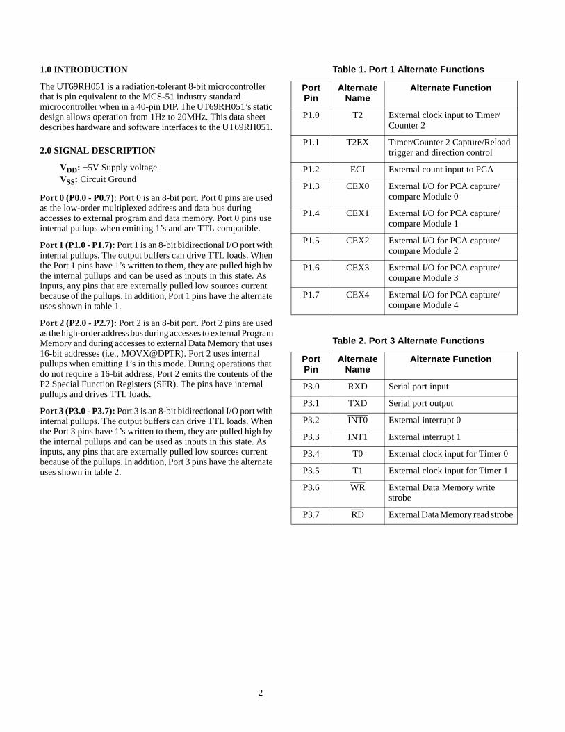
Port 1 (P1.0 - P1.7): Port 1 is an 8-bit bidirectional I/O port with internal pullups. The output buffers can drive TTL loads. When the Port 1 pins have 1’s written to them, they are pulled high by the internal pullups and can be used as inputs in this state. As inputs, any pins that are externally pulled low sources current because of the pullups. In addition, Port 1 pins have the alternate uses shown in table 1.
Port 2 (P2.0 - P2.7): Port 2 is an 8-bit port. Port 2 pins are used as the high-order address bus during accesses to external Program Memory and during accesses to external Data Memory that uses 16-bit addresses (i.e., MOVX@DPTR). Port 2 uses internal pullups when emitting 1’s in this mode. During operations that do not require a 16-bit address, Port 2 emits the contents of the P2 Special Function Registers (SFR). The pins have internal pullups and drives TTL loads.
Port 3 (P3.0 - P3.7): Port 3 is an 8-bit bidirectional I/O port with internal pullups. The output buffers can drive TTL loads. When the Port 3 pins have 1’s written to them, they are pulled high by the internal pullups and can be used as inputs in this state. As inputs, any pins that are externally pulled low sources current because of the pullups. In addition, Port 3 pins have the alternate uses shown in table 2.
Table 1. Port 1 Alternate Functions
Table 2. Port 3 Alternate Functions
Port Pin
Alternate Name
Alternate Function
P1.0 T2 External clock input to Timer/Counter 2
P1.1 T2EX Timer/Counter 2 Capture/Reload trigger and direction control
P1.2 ECI External count input to PCA
P1.3 CEX0 External I/O for PCA capture/compare Module 0
P1.4 CEX1 External I/O for PCA capture/compare Module 1
P1.5 CEX2 External I/O for PCA capture/compare Module 2
P1.6 CEX3 External I/O for PCA capture/compare Module 3
P1.7 CEX4 External I/O for PCA capture/compare Module 4
Port Pin
Alternate Name
Alternate Function
P3.0 RXD Serial port input
P3.1 TXD Serial port output
P3.2 INT0 External interrupt 0
P3.3 INT1 External interrupt 1
P3.4 T0 External clock input for Timer 0
P3.5 T1 External clock input for Timer 1
P3.6 WR External Data Memory write strobe
P3.7 RD External Data Memory read strobe

3
RST: Reset Input. A high on this input for 24 oscillator periods while the oscillator is running resets the device. All ports and SFRs reset to their default conditions. Internal data memory is undefined after reset. Program execution begins within 12 oscillator periods (one machine cycle) after the RST signal is brought low. RST contains an internal pulldown resistor to allow implementing power-up reset with only an external capacitor.
ALE: Address Latch Enable. The ALE output is a pulse for latching the low byte of the address during accesses to external memory. In normal operation, the ALE pulse is output every sixth oscillator cycle and may be used for external timing or clocking. However, during each access to external Data Memory (MOVX instruction), one ALE pulse is skipped.
PSEN: Program Store Enable. This active low signal is the read strobe to the external program memory. PSEN activates every sixth oscillator cycle except that two PSEN activations are skipped during external data memory accesses.
EA: External Access Enable. This pin should be strapped to VSS (Ground) for the UT69RH051.
XTAL1: Input to the inverting oscillator amplifier.
XTAL2: Output from the inverting oscillator amplifier.
2.1 Hardware/Software Interface
2.1.1 MemoryThe UT69RH051 has a separate address space for Program and Data Memory. Internally, the UT69RH051 contains 256 bytes of Data Memory. It addresses up to 64Kbytes of external Data Memory and 64Kbytes of external Program Memory.
2.1.1.1 Program MemoryThere is no internal program memory in the UT69RH051. All program memory is accessed as external through ports P0 and P2. The EA pin must be tied to VSS (ground) to enable access to external locations 0000H through 7FFFH. Following reset, the UT69RH051 fetches the first instruction at address 0000h.
2.1.1.2 Data MemoryThe UT69RH051 implements 256 bytes of internal data RAM. The upper 128 bytes of this RAM occupy a parallel address space to the SFRs. The CPU determines if the internal access to an address above 7FH is to the upper 128 bytes of RAM or to the SFR space by the addressing mode of the instruction. If direct addressing is used, the access is to the SFR space. If indirect addressing is used, the access is to the internal RAM. Stack operations are indirectly addressed so the upper portion of RAM can be used as stack space. Figure 3 shows the organization of the internal Data Memory.
The first 32 bytes are reserved for four register banks of eight bytes each. The processor uses one of the four banks as its working registers depending on the RS1 and RS0 bits in the PSW SFR. At reset, bank 0 is selected. If four register banks are not required, use the unused banks as general purpose scratch pad memory. The next 16 bytes (128 bits) are individually bit addressable. The remaining bytes are byte addressable and can be used as general purpose scratch pad memory. For addresses 0 - 7FH, use either direct or indirect addressing. For addresses larger than 7FH, use only indirect addressing.
In addition to the internal Data Memory, the processor can access 64Kbytes of external Data Memory. The MOVX instruction accesses external Data Memory.
2.1.2 Special Function RegistersTable 3 contains the SFR memory map. Unoccupied addresses are not implemented on the device. Read accesses to these addresses will return unknown values and write accesses will have no effect.

4
(T2) P1.0(T2EX) P1.1(ECI) P1.2(CEX0) P1.3(CEX1) P1.4(CEX2) P1.5(CEX3) P1.6(CEX4) P1.7
RST(RXD) P3.0(TXD) P3.1(INT0) P3.2(INT1) P3.3(T0) P3.4(T1) P3.5(WR) P3.6(RD) P3.7
XTAL2XTAL1
VSS
VDDP0.0 (AD0)P0.1 (AD1)P0.2 (AD2)P0.3 (AD3)P0.4 (AD4)P0.5 (AD5)P0.6 (AD6)P0.7 (AD7)EAALEPSENP2.7 (A15)P2.6 (A14)P2.5 (A13)P2.4 (A12)P2.3 (A11)P2.2 (A10)P2.1 (A9)P2.0 (A8)
12345678910111213141516
1817
1920
40393837363534333231302928272625
2324
2221
VSS(T2) P1.0(T2EX) P1.1
NC(ECI) P1.2(CEX0) P1.3(CEX1) P1.4(CEX2) P1.5(CEX3) P1.6(CEX4) P1.7 RST(RXD) P3.0(TXD) P3.1(INTO) P3.2(INT1) P3.3(TO) P3.4(T1) P3.5(WR) P3.6(RD) P3.7
XTAL2
P0.0 (AD0)P0.1 (AD1)P0.2 (AD2)P0.3 (AD3)P0.4 (AD4)P0.5 (AD5)P0.6 (AD6)P0.7 (AD7)EAALEPSENP2.7 (A15)P2.6 (A14)P2.5 (A13)P2.4 (A12)P2.3 (A11)P2.2 (A10)
12345678910111213141516
1817
1920
44434241403938373635343332313029
2728
2625
2122
2423
XTAL1VSS VDD
P2.1 (A9)P2.0 (A8)NC
VDD
Figure 2a. UT69RH051 40-Pin DIP Connections
Figure 2b. UT69RH051 44-Pin Flatpack Connections

5
Figure 3. Internal Data Memory Organization
2.1.3 ResetThe reset input is the RST pin. To reset, hold the RST pin high for a minimum of 24 oscillator periods while the oscillator is running. The CPU generates an internal reset from the external signal. The port pins are driven to the reset state as soon as a valid high is detected on the RST pin.
While RST is high, PSEN and the port pins are pulled high; ALE is pulled low. All SFRs are reset to their reset values as shown in table 3. The internal Data Memory content is indeterminate.
The processor will begin operation one machine cycle after the RST line is brought low. A memory access occurs immediately after the RST line is brought low, but the data is not brought into the processor. The memory access repeats on the next machine cycle and actual processing begins at that time.
F8
F0
88
80
78
70
•••
38
30
28
20
18
10
08
00
FF
F7
8F
87
7F
77
•••3F
37
2F
27
1F
17
0F
07
•••
•••
INDIRECTACCESS
ONLY
DIRECT OR INDIRECT ACCESS
SCRATCH PAD AREA
BITADDRESSABLE
SEGMENT
REGISTERBANKS
8 BYTES

6
Notes:1. Values shown are the reset values of the registers.2. X = undefined.
Table 3. SFR Memory Registers
F8 CH00000000
CCAP0HXXXXXXXX
CCAP1HXXXXXXXX
CCAP2HXXXXXXXX
CCAP3HXXXXXXXX
CCAP4HXXXXXXXX
FF
F0 B00000000
F7
E8 CL00000000
CCAP0LXXXXXXXX
CCAP1LXXXXXXXX
CCAP2LXXXXXXXX
CCAP3LXXXXXXXX
CCAP4LXXXXXXXX
EF
E0 ACC00000000
E7
D8 CCON00X00000
CMODOOXXX000
CCAPM0X00000000
CCAPM1X00000000
CCAPM2X00000000
CCAPM3X00000000
CCAPM4X00000000
DF
D0 PSW00000000
D7
C8 T2CON00000000
T2MODXXXXXX00
RCAP2L00000000
RCAP2H00000000
TL200000000
TH200000000
CF
C0 C7
B8 IPX0000000
SADEN00000000
BF
B0 P311111111
IPHX00000000
B7
A8 IE00000000
SADDR00000000
AF
A0 P211111111
A7
98 SCON00000000
SBUFXXXXXXXX
9F
90 P111111111
97
88 TCON00000000
TMOD00000000
TL000000000
TL100000000
TH000000000
TH100000000
8F
80 P011111111
SP00000111
DPL00000000
DPH00000000
PCON00XX00XX
87
7
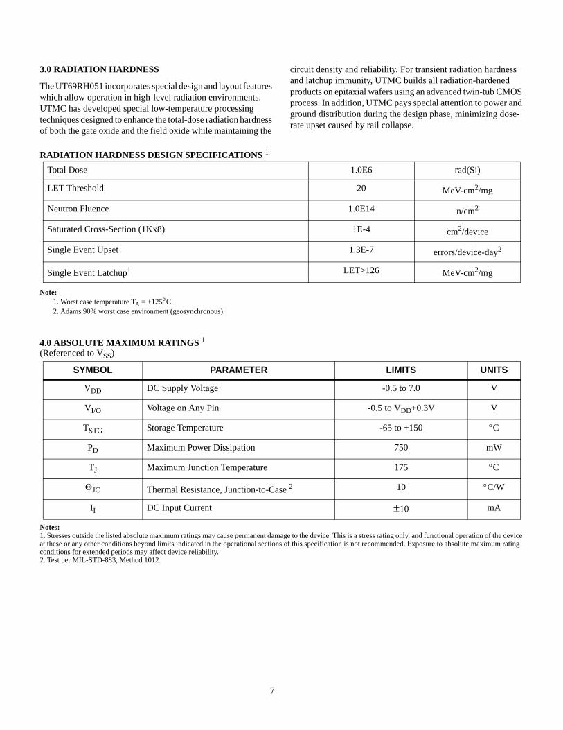
3.0 RADIATION HARDNESS
The UT69RH051 incorporates special design and layout features which allow operation in high-level radiation environments. UTMC has developed special low-temperature processing techniques designed to enhance the total-dose radiation hardness of both the gate oxide and the field oxide while maintaining the
circuit density and reliability. For transient radiation hardness and latchup immunity, UTMC builds all radiation-hardened products on epitaxial wafers using an advanced twin-tub CMOS process. In addition, UTMC pays special attention to power and ground distribution during the design phase, minimizing dose-rate upset caused by rail collapse.
RADIATION HARDNESS DESIGN SPECIFICATIONS 1
Note:1. Worst case temperature TA = +125°C. 2. Adams 90% worst case environment (geosynchronous).
4.0 ABSOLUTE MAXIMUM RATINGS 1(Referenced to VSS)
Notes:1. Stresses outside the listed absolute maximum ratings may cause permanent damage to the device. This is a stress rating only, and functional operation of the device at these or any other conditions beyond limits indicated in the operational sections of this specification is not recommended. Exposure to absolute maximum rating conditions for extended periods may affect device reliability.2. Test per MIL-STD-883, Method 1012.
Total Dose 1.0E6 rad(Si)
LET Threshold 20 MeV-cm2/mg
Neutron Fluence 1.0E14 n/cm2
Saturated Cross-Section (1Kx8) 1E-4 cm2/device
Single Event Upset 1.3E-7 errors/device-day2
Single Event Latchup1 LET>126 MeV-cm2/mg
SYMBOL PARAMETER LIMITS UNITS
VDD DC Supply Voltage -0.5 to 7.0 V
VI/O Voltage on Any Pin -0.5 to VDD+0.3V V
TSTG Storage Temperature -65 to +150 °C
PD Maximum Power Dissipation 750 mW
TJ Maximum Junction Temperature 175 °C
ΘJC Thermal Resistance, Junction-to-Case 2 10 °C/W
II DC Input Current ±10 mA

8
5.0 DC ELECTRICAL CHARACTERISTICS (Pre/Post-Radiation)*VDD = 5.0V ±10%; TA = -55°C < TC < +125°C)
Notes: * Post-radiation performance guaranteed at 25°C per MIL-STD-883.1. Under steady state (non-transient) conditions, IOL must be limited externally as follows:
Maximum IOL per port pin: 10mAMaximum IOL per 8-bit port- Port 0: 26mA
Ports 1, 2, & 3: 15mAMaximum total IOL for all output pins: 71mA
If IOL exceeds the test condition, VOL may exceed the related specification. Pins are not guaranteed to sink current greater than the listed test conditions.2. Capacitive loading on ports 0 and 2 may cause spurious noise pulses to be superimposed on the VOL of ALE and ports 1 and 3. The noise is due to external bus
capacitance discharging into the port 0 and port 2 pins when these pins make 1 to 0 transitions during bus operations. In applications where capacitance loading exceeds 100 pF, the noise pulse on the ALE may exceed 0.8V. In these cases, it may be desirable to qualify ALE with a schmitt trigger or use an address latch with a schmitt trigger strobe input.
3. Capacitive loading ports 0 and 2 cause the VOH on ALE and PSEN to drop below the VDD-0.3 specification when the address lines are stabilizing.
SYMBOL PARAMETER CONDITION MINIMUM MAXIMUM UNITVIL Low-level Input Voltage 0.8 VVIH High-level Input Voltage
(except XTAL, RST)2.0 V
VIH1 High-level Input Voltage(XTAL, RST)
3.85 V
VOL Low-level Output Voltage1
(Ports 1, 2 and 3)IOL = 100µA 0.3 V
IOL = 1.6mA 0.45 VIOL = 3.5mA 1.0 V
VOL1 Low-level Output Voltage1,2
(Port 0, ALE, PSEN, PROG)IOL = 200µA 0.3 V
IOL = 3.2mA 0.45 VIOL = 7.0mA 1.0 V
VOH High-level Output Voltage3
(Ports 1, 2, and 3ALE/PROG and PSEN)
IOH = -10µA 4.2 V
IOH = -30µA 3.8 VIOH = -60µA 3.0 V
VOH1 High-level Output Voltage(Port 0 in External Bus Mode)
IOH = -200µA 4.2 V
IOH = -3.2mA 3.8 VIOH = -7.0mA 3.0 V
IIL Logical 0 Input Current(Ports 1, 2, and 3)
VIN = 0.0VVCC = 5.5V
-50 µA
IIL Logical 0 Input Current(XTAL 1)
VIN = 0.0VVCC = 5.5V
-65 µA
ILI Input Leakage Current(Port 0)
VIN = 0.0V or VCCVCC = 5.5V
±25 µA
ILI Input Leakage Current(XTAL1)
VIN = 0.0V or VCCVCC = 5.5V
±65 µA
RRST RST pulldown resistor (except EA) 10K 225K ohms
CIO4 Pin Capacitance @ 1MHZ, 25°C 15 pF
IDD Power Supply Current: @16MHz @20 MHz
95120
mA

9
4. Capacitance measured for initial qualification or design changes which may affect the value.
Figure 4. IDD Test Condition, Active ModeAll other pins disconnected
Figure 5. Clock Signal Waveform for IDD Tests in Active and Idle ModestCLCH = tCHCL = 5ns
VDD
VDD
IDDVDD
VDD
RST P0
EA
VSS
XTAL2
XTAL1CLOCKSIGNAL
(NC)
tCLCH = tCHCL = 5nsGND
VDD -0.5
0.45V 0.2 VDD -0.1
0.7 VDD
tCLCLtCHCL
tCHCX
tCHCX
tCLCH

10
6.0 AC CHARACTERISTICS READ CYCLE (Post-Radiation)*(VDD = 5.0V ±10%; -55°C < TC < +125°C)
Note: * Post-radiation performance guaranteed at 25°C per MIL-STD-883 Method 1019 at 1.0E6 rads(Si).1. Guaranteed, but not tested.
SYMBOL PARAMETER MINIMUM MAXIMUM UNIT
tCLCL Clock Period 50 ns
1/tCLCL Oscillator Frequency 20 MHz
tLHLL ALE Pulse Width 2 tCLCL-40 ns
tAVLL Address Valid to ALE Low tCLCL-40 ns
tLLAX1 Address Hold after ALE Low tCLCL-30 ns
tLLIV ALE Low to Valid Instruction 4 tCLCL-100 ns
tLLPL ALE Low to PSEN Low tCLCL-30 ns
tPLPH PSEN Pulse Width 3 tCLCL-45 ns
tPLIV PSEN Low to Valid Instruction In 3 tCLCL-105 ns
tPXIX1 Input Instruction Hold after PSEN 0 ns
tPXIZ1 Input Instruction Float after PSEN tCLCL-25 ns
tAVIV Address to Valid Instruction In 5 tCLCL-105 ns
tPLAZ1 PSEN Low to Address Float 10 ns
tRLRH RD Pulse Width 6 tCLCL-100 ns
tWLWH WR Pulse Width 6 tCLCL-100 ns
tRLDV RD Low to Valid Data In 5 tCLCL-165 ns
tRHDX1
Data Hold After RD High 0 ns
tRHDZ1 Data Float After RD High 2 tCLCL-60 ns
tLLDV ALE Low Valid Data In 8 tCLCL-150 ns
tAVDV Address to Valid Data In 9 tCLCL-165 ns
tLLWL ALE Low to RD or WR Low 3 tCLCL-50 3 tCLCL+50 ns
tAVWL Address Valid to WR Low 4 tCLCL-130 ns
tQVWX Data Valid Before WR High tCLCL-33 ns
tWHQX Data Hold After WR High tCLCL-33 ns
tQVWH Data Valid to WR High 7 tCLCL-150 ns
tRLAZ1 RD Low to Address Float 0 ns
tWHLH RD or WR High to ALE High tCLCL-40 tCLCL+40 ns

11
Figure 6. External Program Memory Read Timing Waveforms
Figure 7. External Data Memory Read Cycle Waveforms
Figure 8. External Data Memory Write Cycle Waveforms
ALEtPLPH
PSEN
tLHLL
tAVLL
tLLPL
tLLIV
PORT 0
PORT 2
tAVIV
A8 - A15 A8 - A15
A0 - A7 A0 - A7INSTR IN
tLLAX
tPLAZtPXIZ
tPXIX
tPLIV
ALEtLHLL
PORT 0
PORT 2
tAVDV
P2.0 - P2.7 OR A8 -A15 FROM DPH A8 - A15 FROM PCH
A0 -A7 FROM RI OR DPL INSTR IN
PSEN
RD
DATA IN A0 - A7 FROM PCL
tAVWL
tLLAX
tWHLH
tLLDV
tLLWLtRLRH
tAVLL
tRLAZ
tRLDV
tRHDZtRHDX
ALEtLHLL
PORT 0
PORT 2 P2.0 - P2.7 OR A8 -A15 FROM DPH A8 - A15 FROM PCH
A0 -A7 FROM RI OR DPL INSTR IN
PSEN
WR
DATA OUT A0 - A7 FROM PCL
tAVWL
tLLAX
tWHLH
tLLWL tWLWH
tAVLL tWHQXtQVWX
tQVWH

12
7.0 SERIAL PORT TIMING CHARACTERISTICS (VDD = 5.0V ±10%; -55°C < TC < +125°C)
Note: 1. Guaranteed, but not tested.
Figure 9. Serial Port Timing Waveforms
8.0 EXTERNAL CLOCK DRIVE TIMING CHARACTERISTICS
Note: 1. Guaranteed, but not tested.
Figure 10. External Clock Drive Timing Waveforms
SYMBOL PARAMETER MINIMUM MAXIMUM UNIT
tXLXL1 Serial Port Clock Period 12 tCLCL-10 12 tCLCL+10 ns
tQVXH Output Data Setup to Clock Rising Edge 10 tCLCL-133 ns
tXHQX Output Data Hold after Clock Rising Edge 2 tCLCL-70 ns
tXHDX1 Input Data Hold after Clock Rising Edge 0 ns
tXHDV Clock Rising Edge to Input Data Valid 10 tCLCL-133 ns
SYMBOL PARAMETER MINIMUM MAXIMUM UNIT
1/tCLCL Oscillator Frequency 20 MHz
tCHCX High Time 16 ns
tCLCX Low Time 16 ns
tCLCH Rise Time 20 ns
tCHCL Fall Time 20 ns
ALE
OUTPUT DATA(WRITE TO SBUF)
CLOCK
0 1 2 3 4 5 6 7 8
TXLXL
TXHQXTQVXH
TXHDX
0 1 2 3 4 5 6 7
TXHDV SET TI
SET RI
INPUT DATA(CLEAR RI)
VALID VALIDVALIDVALIDVALID VALID VALID VALID
tCHCX
tCLCL
tCLCH
tCHCX
VDD - 0.5
0.45 V
0.7 VDD0.2 VDD - 0.1
tCHCL

13
9.0 PACKAGING
Notes:1. All package finishes are per MIL-PRF-38535.2. Letter designations are for cross-reference MIL-STD-1835.
E
0.595+0.010
END VIEW
SIDE VIEW
L0.2000.125
b
0.018 +0.002
0.100e
S20.005 MIN. typ.
D
2.000 +0.025
A0.185 MAX.
TOP VIEW
PIN 1 I.D.(Geometry OPTIONAL)
C0.010 + 0.002
- 0.001
S10.005 MIN. TYP.
0.600
Figure 11. 40-pin Side-Brazed DIP

14
C
Notes:1. All exposed metalized areas to be plated per MIL-PRF-38535.2. Dimension letters refer to MIL-STD-1835.
Figure 12. 44-Lead Flatpack

15
APPENDIX ADifference Between Industry Standard and UT69RH051
The areas in which the UT69RH051 differs from the industry standard will be covered in this section. In this discussion, industry standard will be used generically to refer to all speed grades including the 20MHz.
1.0 RESET
The UT69RH051 requires the RST input to be held high for at least 24 oscillator periods to guarantee the reset is completed in the chip. Also, the port pins are reset asynchronously as soon as the RST pin is pulled high. On the UT69RH051 all portions of the chip are reset synchronously when the RST pin is high during a rising edge of the input clock. When coming out of reset, the industry standard takes 1 to 2 machine cycles to begin driving ALE and PSEN immediately after the RST is removed, but the access during the first machine cycle after reset is ignored by the processor. The second cycle will repeat the access and processing will begin.
2.0 POWER SAVING MODES OF OPERATION
2.1 Idle Mode
Idle mode and the corresponding control bit in the PCON SFR have not been implemented in the UT69RH051. Setting the idle control bit has no effect.
2.2 Power Down Mode
Power down mode and the corresponding control bit in the PCON register have not been implemented in the UT69RH051. Setting the power down control bit has no effect. Also, the Power Off Flag in the PCON has not been implemented.
3.0 ON CIRCUIT EMULATION
The On Circuit Emulation mode of operation in the industry standard has not been implemented in the UT69RH051.
4.0 OPERATING CONDITIONS
The operating voltage range for the industry standard is 5V+20%. The operating temperature range is 0°C to 70°C. On the UT69RH051, the operating voltage range is 5V+10%. The operating temperature range is -55°C to +125°C.

16
APPENDIX BImpact of External Program ROM
The 8051 family of microcontrollers, including the industry standards, use ports 0 and 2 to access external memory. In implementations with external program memory, these two ports
are dedicated to the program ROM interface and can not be used as Input/Output ports. The UT69RH051 uses external program ROM, so ports 0 and 2 will not be available for I/O.

17
ORDERING INFORMATION
UT69RH051 Microcontroller: SMD
Lead Finish:(A) = Solder (C) = Gold(X) = Optional
Case Outline:(Q) = 40-pin DIP(Y) = 44-pin Flatpack
Class Designator:(Q) = Class Q(V) = Class V
Device Type(01) = 8-bit Microcontroller
Drawing Number: 95638
Total Dose: (H) = 1E6 rads(Si) (G) = 5E5 rads(Si) (F) = 3E5 rads(Si) (R) = 1E5 rads(Si)
Federal Stock Class Designator: No options
5962 * 95638 * * * *
Notes:1. Lead finish (A, C, or X) must be specified.2. If an “X” is specified when ordering, part marking will match the lead finish and will be either “A” (solder) or “C” (gold).3. Total dose radiation must be specified when ordering. QML Q and QML V not available without radiation hardening.

18
UT69RH051 Microcontroller
UT **** *** - * * * *
Total Dose:( ) = None
Lead Finish: (A) = Solder (C) = Gold(X) = Optional
Screening:(C) = Mil Temp
(P) = Prototype
Package Type:(P) = 40-pin DIP(W) = 44-pin Flatpack
Device Type:(UT69RH051) = 8-bit Microcontroller
Notes:1. Lead finish (A,C, or X) must be specified.2. If an “X” is specified when ordering, then the part marking will match the lead finish and will be either “A” (solder) or “C” (gold).3. Radiation characteristics are neither tested nor guaranteed and may not be specified.4. Devices have prototype assembly and are tested at 25°C only. Radiation characteristics are neither tested nor guaranteed and may not be specified.

19
Notes