Embed Size (px)
Citation preview

External Use
TM
Using the Design Checklist for
Board Bring-Up
FTF-NET-F0137
A P R . 2 0 1 4
Satoshi Iida | Application Engineering Manager

TM
External Use 1
Agenda
• Introduction and Assumptions
• Pre-prototype board arrival phase
• Initial board power on / validation
TM
External Use 2
Introduction and Assumptions
• The purpose of this presentation is to help hardware and software engineers developing systems using QorIQ T4 series products
− We will cover debug procedures to successfully validate HW design to a point where it is reasonable to begin SW development
Pre-board arrival activities
Initial board power up and validation of basic operation
Boot loader installation and initialization
• System assumptions
− Boot loader is U-Boot and is located in NOR flash at power up
− U-boot is configured to run initially from NOR flash but transfer to DDR at run time
− U-Boot run on Core 0
− CodeWarrior is the the HW debugger used
− No secure boot implementation

TM
External Use 3
Pre-Prototype Board Arrival
Phase
This section provides hardware and firmware developer steps to
prepare for new target arrival to the lab

TM
External Use 4
Collecting Technical Information
• Please ensure you are familiar with the following Freescale
collateral:
− T4240 QorIQ Advanced Multicore Processor Data Sheet (T4240EC) /
T4160 QorIQ Advanced Multicore Processor Data Sheet (T4160EC)
/T4080 QorIQ Advanced Multicore Processor Data Sheet (T4080EC)
− T4240 QorIQ Advanced Multiprocessing Processor Reference Manual
(T4240RM)
− T4240, T4160 and T4080 Chip Errata (T4240CE)
− T4240 QorIQ Integrated Processor Design Checklist (AN4559)
− Hardware and Layout Design Considerations for DDR3 SDRAM Memory
Interfaces (AN3940)
− Difference Between T4240 Rev 1 and T4240 Rev 2 (AN4713)

TM
External Use 5
Board Design Considerations
• Several collateral pieces are available to
assist with schematic and board layout
• Listed here are sections that are critical to
successful board bring-up

TM
External Use 6
Board Design Considerations (continued)
• Booting the T4240
− Select your boot method
NOR
NAND
SPI
• Socket the flash for initial board bring-up
PCI Ex / SRIO
• Booting from these requires special consideration that is outside of scope of this session
Note: Rev 1 T4240 have an erratum (A-005878) preventing PBL/RCW loading from NOR
and NAND. RCW load must select different source or use I2C boot sequencer to work
around the erratum. Rev 2 do have this fixed and no longer an issue.

TM
External Use 7
Board Design Considerations (continued)
• Booting T4240
− Connect the power on reset configuration pins appropriately
See “Power – On Reset Configuration” section of RM
• Personality pins
− Personality and test pins include SCAN_MODE_B and TEST_SEL_B
− Engineering use pins (such as ASLEEP) must not inadvertently be pulled down externally during POR
− Look at the pin-out table in the data sheet (T4240EC or T4160EC) for pins marked with a warning against
being pulled down during power-on reset
Reset request
• The T4240 has a RESET_REQ_B pin which would normally request a reset of the device via
the PORESET_B or HRESET_B pins
• In production, connecting the reset request output to PORESET or HRESET input is desirable,
indicating a significant and often unrecoverable error has occurred in the system
• During system prototyping, it is recommended to temporarily sever this connection, as
unintended reset loops can occur and tying RESET_REQ_B back to PORESET_B or
HRESET_B can make it more difficult to determine the cause

TM
External Use 8
• Connect the power on reset configuration pins appropriately
• Make the ASLEEP signal accessible to a scope probe
The state of this pin can offer important information about the reset status of the
device
• Using FPGA or CPLD to connect reset signal or drive configuration
pins?
Ensure a basic programming image is available that connects debugger and
reset signals correctly
If RESET_REQ_B is connected to the FPGA, it shouldn’t reset the T4240 during
initial debugging
Board Design Considerations (continued)

TM
External Use 9
Board Design Considerations (continued)
• Clock sources
− Ensure all required clock sources are driven, and their oscillators and
drivers meet the data sheet specifications for voltage, rise/fall time, and
jitter
SYSCLK and DDRCLK must always be driven
ECn_GTX_CLK125 must be driven if RGMII mode is used on the respective
ECn port
• Single-ended clocking requirements are provided in the “Input clocks” section of the data
sheet
SerDes reference clocks (SDn_REF_CLKn and SDn_REF_CLKn_B) must be
driven if the corresponding SerDes bank is enabled in the RCW
• SerDes reference clock requirements are provided in the data sheet
Optional input clock sources include RTC, USBCLK, and TSEC_1588_CLK_IN

TM
External Use 10
Board Design Considerations (continued)
• Voltage ID (VID) Controllable supply
− To guarantee performance and power specifications, a specific method of
selecting the optimum voltage-level must be implemented when the chip is used.
As part of the chip’s boot process, software must read the VID efuse values
stored in the Fuse Status register (FUSESR) and then configure the external
voltage regulator based on this information. This method requires a point of load
voltage regulator for each chip
− During the power-on reset process, the fuse values are read and stored in the
FUSESR. It is expected that the chip's boot code reads the FUSESR value very
early in the boot sequence and updates the regulator accordingly.
− The default voltage regulator setting that is safe for the system to boot is the
recommended operating VDD at initial start-up of 1.05V. It is highly
recommended to select a regulator with a Vout range of at least 0.9V to 1.1V,
with a resolution of 12.5mV or better, when implementing a VID solution.

TM
External Use 11
Board Design Considerations (continued)
• Reset Configuration Word (RCW)
− Study the RCW to ensure all PLL ratios and I/O connections are selected appropriately
If you plan to support multiple speed grades of device or memory
• Pre-select SYSCLK and DDRCLK frequencies and PLL multipliers to ensure desired CPU core and platform frequency options are achievable
− If some SerDes lanes are unused on your custom board, disable those lanes in the RCW
Disable all the lanes of each unused bank and do not provide a SerDes reference clock for any unused bank
− QCS should be used as a tool to help you select an appropriate RCW
It generates CRC checksums to produce your Pre Boot Loader (PBL) output file
− Consider using an RCW source that allows you additional space to include pre-boot initialization(PBI)
This allows you to implement errata workarounds and other custom internal register programming prior to boot

TM
External Use 12
Board Design Considerations (continued)
• DDR3 connections
− Compare layout with recommendations in AN3940
− Ensure Vtt and MVREF are driven by appropriate sources. The T4240
has strict voltage requirements on MVREF, which must closely track
GVDD/2. Use of DDR3 integrated device which generates Vtt and VREF
is highly recommended
Link for QorIQ Configuration Suite

TM
External Use 13
Installing and Leveraging Freescale Development Tools
• This section lists suggested steps one can
take to prepare / learn about tools available
prior to T4240 based board arrival

TM
External Use 14
Install the QCS Tool Suite: Focus on PBL and DDR/DDRv
• The QorIQ Configuration Suite (QCS) helps you configure the
T4240
− QCS is well-documented and will allow you to focus on the PBL, DDR
and DDRv modules in QCS
− Please follow the QorIQ Configuration Suite Installation Guide

TM
External Use 15
PBL Tool
• See the Freescale website to download the QCS tools
• Using the QCS Quick Start guide, install and use QCS to come up
with RCW settings and double-check the custom changes with your
local Freescale technical representative
• It’s important for proper pre-boot initialization of the device to have
a valid RCW for your selected clocking values and SerDes
configuration.
• Any custom configurations you develop should be in compliance
with both the T4240 Reference Manual RCW options and what the
RCW sub-tool under QCS allows
TM
External Use 16
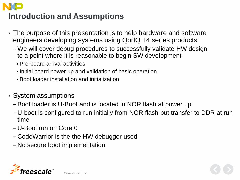
QCS
• After generation of your proposed RCW settings, it’s important to
review these with your Freescale technical representative
• Work with importing existing RCW files as a good starting point

TM
External Use 17
Use QCS to Come Up with DDR Settings
• Another key part of getting a smooth bring-up is to at least
have working DDR controller parameters
− Signal Integrity engineers should simulate DDR connection traces and
confer with FSL technical representative
− If using compatible DIMMs on future prototypes, try these in FSL target.
Before your custom target arrives, it can be useful to place your DIMMs into the
Freescale target to see what controller parameters are
− Board-specific parameters: Please note your custom target will require a
different set of parameters than those used by the Freescale
development system
Some parameters are affected by the layout of the board.
These parameters include DDRx_DDR_SDRAM_CLK_CNTL[CLK_ADJUST]
and DDRx_DDR_WRLVL_CNTL[WRLVL_START]

TM
External Use 18
Use QCS to Come Up with DDR Settings (continued)

TM
External Use 19
Practice Using DDRv on T4240QDS
• After getting a range of working values for the DDR controller settings for the
T4240, your next step is to use the DDRv tool that is part of QCS
• If your target has met the minimal requirement for the DDRv optimization tool, you
can use it on your target to show a range of values
• In this range is a “centered” value that is recommended as “best for your target”
Before discovering all
the features of this tool
on your custom target, it
is highly advised that you
run this DDRv tool
successfully on the
Freescale T4240QDS
target.
Also note availability of
application note
specifically targeting
DDR register setting
such as AN4039.

TM
External Use 20
CodeWarrior Debugger
• If you are new to the CodeWarrior debug environment, now is a
great time to install and start using the basics in debugging with
your Freescale T4240QDS target
• You can use the debugger or rather the sub-tool communications
shell CCS, to run boot utilities if your RCW does not bring your SoC
out of reset
• You can use the debugger for basic U-Boot debug and just
accessing memory
• Once installed you can see a lot of good documents found under
C:\Freescale\CW_PA_v10.x.x\PA

TM
External Use 21
Verify Installation of All Necessary Tools
• CodeWarrior
• JTAG boundary scan tools
• I2C EEPROM burner
• CPLD tools

TM
External Use 22
Verify Installation of All Necessary Tools (continued)
• Install CW PA10 and make sure you can connect to the FSL
T4240 target
• Confirm that you can do RCW over-ride on the FSL target and
confirm the different RCW results by reading the RCW registers in
the device
• If using SPI boot, confirm the method on FSL target and then
confirm the debugger connection
− COP delay needed for longer boot time due to RCW + BI + u-boot.bin load

TM
External Use 23
Verify JTAG Connection in Schematics
• For example: Independent TRESET# and PORESET#
− Look out for FPGAs passing signals between the COP/JTAG

TM
External Use 24
Try to Modify U-Boot for the Memory-Map and Try Running
on the FSL T4240QDS Target
• Install U-Boot sources and cross tool chain
− Confirm environment variables and confirm builds for the FSL T4240 and
test if the newly built image works
• Start to develop your custom U-Boot configurations
− For example: u-boot/include/configs/<custom_name>T4240.config
• Build your modified U-Boot for the FSL target and flash it using the
CW debugger
− This is important, as you’ll be practicing for the prototype flashing
• Confirm that the flash device you are using is supported in the CW
debugger

TM
External Use 25
Socket the Flash Device
• Where the RCW, PBI and U-Boot code is located
− This is helpful if the debugger does not work on the new prototype
boards
This way you can flash externally
Make sure your lab-based flash programmer is working with the prototype
board’s flash device
• Application note on how to add new flash device can be found at.
C:\Freescale\CW_PA_v10.3.3\PA\PA_Tools\FlashToolKit\Document
ation

TM
External Use 26
Initial Board Power On/Validation

TM
External Use 27
Confirm Reset Sequence
• When prototype boards are received they may or may not have the requisite personalization information programmed
• The hardware design must ensure this board-specific data, including the RCW and PBL information, is programmed into the appropriate memory parts on the board
• Programming of board-specific elements that are not directly related to T4240 operation are beyond the scope of this presentation.
− CPLD, power sequencers
• If these non-T4240 elements are required to get the T4240 into an operative state then the HW designer must either program these without the use of T4240 debug resource or ensure these mechanisms may be temporarily bypassed such that the T4240 can operate without them

TM
External Use 28
T4240 Reset Sequence
• The successful completion of the reset sequence is indicated by the ASLEEP signal being driven low as shown in the timing diagram
• If this does not occur, then there is an issue with the reset sequence – usually with some basic hardware function – and it must be debugged using low-level hardware debug tools and techniques (logic analyzer and oscilloscopes)

TM
External Use 29
T4240 Reset Sequence (continued)
• Things to check if the reset hardware reset sequence does not complete include:
− Voltage Rails: Ensure the all the required voltage levels are provided and meet the
specified levels and tolerances
Ensure that the recommended power rail sequence is followed
− SYSCLK. Ensure it is present and meets the voltage level, slew rate, frequency, duty cycle,
and jitter requirements specified
− Reset Signals: Ensure PORESET is driven for a minimum of 1 ms and that it is driven
before the core and platform voltages are powered up
If HRESET is driven externally, ensure it is released as expected; if driven just by the T4240, confirm
it is released after PORESET desertion
− Confirm the RCW device is being read after ASLEEP is driven high
If not, check that the cfg_rcw_src signals are driven as expected when the PORESET signal is released
− Confirm RCW contents are as expected. The specifics of the RCW must match the system
configuration
NOTE: If the RCW device is blank, a tool such as CodeWarrior must be used to program this. Instructions
for doing this are provided in later in this presentaion. However, it is recommended to confirm the hardware
operation as much as possible before connecting this tool. Confirming that the T4240 at least attempts to
read the RCW device is a good checkpoint.

TM
External Use 30
T4240 Reset Sequence (continued)
• Confirm that the PBL information is read. Note that this occurs
after the RCW is read, even if the PBL and RCW device are the
same. The PBL reads start but the ASLEEP never is driven low, the
likely failure is that some PBL action is attempting to configure the
part in an undefined or unexpected way
• Confirm the PBL actions are as defined for the system. If the
desired PBL action is involved, it is recommended to start with the
simplest possible PBL contents (to address erratum) and confirm
that the reset sequence completes
• Then add other PBL configurations in a staged manner

TM
External Use 31
Connect Debug Tools
• At this point, we are ready to connect to the target via a debugger. For the purposes of this presentation, we focus on Freescale’s CodeWarrior 10.x debugger. An evaluation version of the CodeWarrior development tool can be obtained from Freescale
• Debugger documentation can be found within the product install directory. This would typically be located at:
C:\Program Files\Freescale\CW PA v10.xx\PA\Help\PDF
• Follow the Targeting _PA_Processors.pdf document for more information on how to get started with CodeWarrior

TM
External Use 32
Tap Connection
• TAP is now needed to physically connect to
the hardware
• This could be a USB TAP, Ethernet TAP, or
newer CodeWarrior TAP
• The TAP should be connected to a standard
16-pin COP header on the board such that
pin 1 of the header is aligned with the red
stripe down the TAP ribbon cable.

TM
External Use 33
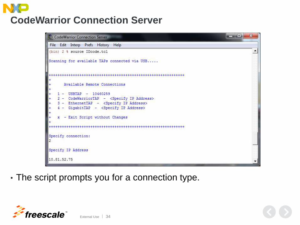
Confirm Processor with CCS
• IDE as well as CodeWarrior Connection Server (CCS)
• To verify connectivity, first launch the CodeWarrior Connection Server
• This is a command converter that converts Debugger actions into
actionable commands for the TAP
• CCS starts minimized in the PC system tray
• Double click the CCS icon in the PC system tray to launch the full screen
window
• CCS supports TCL scripting, and it comes with some TCL scripts which
may be useful in initial board bring-up
• The JTAG connection script scans the JTAG bus and reports to the
IDCODE of anything found
• To run this script, within CCS type in: source IDcode.tcl
TM
External Use 34
CodeWarrior Connection Server
• The script prompts you for a connection type.

TM
External Use 35
CodeWarrior Connection Server (continued)
• CCS presents you with three commands
• The command scanboard scans the JTAG chain
• After running the scanboard command, you are presented with the JTAG chain of the board

TM
External Use 36
CodeWarrior Connection Server (continued)
• Here shows a connection to a single T4240 device
• This verifies connectivity between a developer’s host PC, through
the TAP to the board and processor

TM
External Use 37
Connecting CodeWarrior to Target Board
• At this point, we have verified that the processor powers up and responds to JTAG commands, as well as connectivity from the host PC to the processor
• The next step is to connect to the target with the debugger interface
• Upon launching CodeWarrior, the first dialog box asks you to specify a workspace
• A workspace is a folder intended to contain all work, including configuration settings of tool, debug connections, and even data to be compiled and or downloaded--
TM
External Use 38
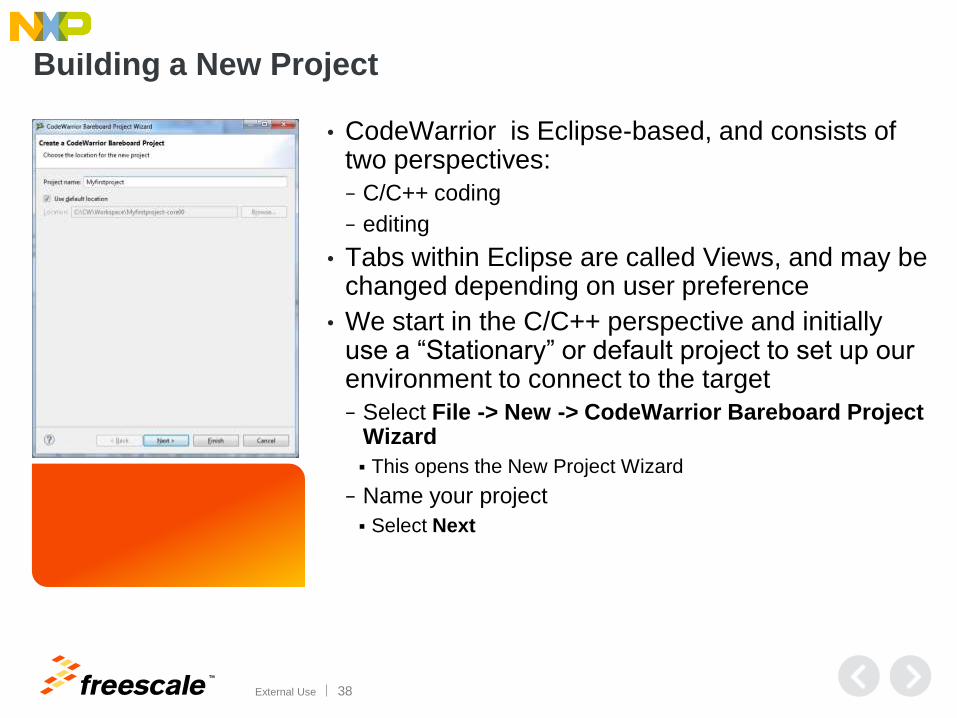
Building a New Project
• CodeWarrior is Eclipse-based, and consists of two perspectives:
− C/C++ coding
− editing
• Tabs within Eclipse are called Views, and may be changed depending on user preference
• We start in the C/C++ perspective and initially use a “Stationary” or default project to set up our environment to connect to the target
− Select File -> New -> CodeWarrior Bareboard Project Wizard
This opens the New Project Wizard
− Name your project
Select Next

TM
External Use 39
Selecting Processor

TM
External Use 40
Debug Target Setting

TM
External Use 41
Build settings

TM
External Use 42
Configuration

TM
External Use 43
Trace Configuration

TM
External Use 44

TM
External Use 45
Building project
• Build project (even though you are not building any code)
• Right click on project or hammer

TM
External Use 46
CFG File
• The project just created consists of some
example code that can be compiled via
CodeWarrior and downloaded to the target.
Additionally, it consists of configuration files,
which are essentially TCL scripts, to be
downloaded to the target prior to code
executing. The intent of the CFG files is to
enable configuration of the processor, such
as the DDR or flash controllers, prior to
programming flash or executing code
developed within CodeWarrior
• In some sense, the CFG file does the job of
a bootloader, such as U-Boot

TM
External Use 47
Accessing Debug Configuration
• Connections to the target are known as “Debug Configurations”
• To access the debug configuration for a project, right click on the
small downward pointing arrow next to the bug icon on the toolbar
and select Debug Configurations
• Note that this can also be opened through the menu under Run –>
Debug Configurations

TM
External Use 48
Connecting to Target (continued)
• For an initial connection to the target, we want to attempt to
connect without any CFG file
− To de-select the CFG file from our default project:
• Select your project from under the “CodeWarrior” section on the left
hand column

TM
External Use 49
Connecting to Target (continued)
• Edit the Connection Type

TM
External Use 50
Connecting to Target (continued)
• Edit the Target core
• Deselect any checkboxes under the “initialize target” column

TM
External Use 51
Connecting to Target (continued)
• Edit the Target memory
• Deselect any checkboxes under the “initialize target” column
• Click OK twice, to get back to Debug Configurations
• Click Debug to connect to the target with the debugger

TM
External Use 52
Using CodeWarrior to Provide the RCW
• An RCW can be loaded from various sources, including interfaces
such as I2C or flash
− If JTAG boundary scan is not able to program the RCW, it is possible to
force an RCW into the processor via the CodeWarrior debugger
• To do this, first create a file that creates information on the JTAG
scan chain and intended RCW
− There are examples of such a file in the CodeWarrior install:
C:\Program Files\Freescale\CW PA
v10.x.x\PA\PA_Support\Initialization_Files\jtag_chains

TM
External Use 53
Example JTAG Configuration File
# Example file to allow overriding the whole RCW or only parts of it
#
# Syntax:
# T4240 (2 RCW_option) (RCWn value) ...
#
# where:
# RCW_option = 0 [RCW Override disabled]
# 1 [RCW Override enabled]
# 2 [Reset previous RCW Override parts]
# 0x80000001 [RCW Override + PLL Override]
# NOTE: Enabling PLL Override could lead to hanging the chip
#
# RCWn = 21000+n (n = 1 .. 16; index of RCW value)
#
# value = 32bit value
T4240 (2 1) (210001 0x14180019) (210002 0x0c10190c) (210003 0x00000000) (210004 0x00000000) (210005 0x70023060) (210006 0x0055bc00) (210007 0x1c020000) (210008 0x09000000) (210009 0x00000000) (210011 0xee0000ee) (210012 0x00000000) (210013 0x000187fc) (210014 0x00000000) (210015 0x00000000) (210016 0x00000008)
First two words are ignored and not used to replace the RCW in the active system. As we are using 2, 1
If option of 0x80000001 is used PLL will be override

TM
External Use 54
Instructing CW to Use JTAG Configuration File
• To instruct CodeWarrior to use the JTAG configuration file, first bring up the Debug Configuration intended
• Select the debug configuration to be used, and select the “Edit” Button next to connection type
• Select Edit, for System
• Select Edit once more, for System Type

TM
External Use 55
Instructing CW to Use JTAG Configuration File (continued)
Select Import, and import the previously created JTAG file
• Upon connecting to the target, the RCW defined in the JTAG configuration file is forced into the
processor
‒ Needed for cases where flash or EEPROM is blank
‒ In such a case, a developer may force an RCW with CodeWarrior, program the flash manually, and then
revert back to the fetched RCW

TM
External Use 56
Running the CodeWarrior HW Debugger
• When the debugger launches, the Eclipse perspective changes to the debug
perspective
• Upon successfully connecting to the processor, the Debug view should change,
highlighting the thread executing
• The start / stop / pause / step icons should also be highlighted
• As we see here, the processor code is halted at the reset vector, 0xFFFFFFFC
• We now can verify some basic settings
‒ This can be done in either view: the GUI or a Debugger Command Shell
‒ To add the command shell to the debug perspective go to Window -> Show
View - > Command Shell

TM
External Use 57
Verify POR Settings
• The registers tab contains all registers within the processor
• Upon clicking on a register, the bit fields of that register should
be expanded

TM
External Use 58
Verifying RCW
• At this point, one could verify the RCW read in by the processor, as well as some
basic configuration that the RCW sets up
• Through the command shell, it’s easy to verify reads and writes to memory-
mapped registers within the processor
• For example, you could verify a read to CCSRBAR returns a pointer to the
CCSRBAR

TM
External Use 59
CodeWarrior Initialization Files
• Upon successfully connecting to a target, and verifying reads / writes to internal memory, it is now possible to start initializing interfaces such as memory
− CodeWarrior initialization files are intended for this purpose
• Sample configuration files are part of the CodeWarrior install:
C:\Program Files\Freescale\CW PA v10.x.x\PA\PA_Support\Initialization_Files
• They should also be part of the default CodeWarrior stationary project for a given processor. The initialization file is essentially a script that executes within CodeWarrior to pre-load registers on the processor prior to code execution
− Typical functions include setting up TLB’s, LAW’s, DDR, and flash interface
• Internal to the processor, a portion of CPC cache may be converted into private SRAM
− Initially, we use a CFG file to set up the cache as private SRAM and set up the flash interface so that we can program flash
• Within the Initialization Files directory of the install, you should find T4240QDS_init_sram.tcl configuration file that can be used as a starting point for such a purpose
− Make a copy of the original, and modify it for your flash configuration.

TM
External Use 60
Sample Initialization File
• Below is a sample section from such a file, where the CPC is set up
to behave as SRAM
− Please note that a LAW and TLB entry is needed for the SRAM

TM
External Use 61
Sample Initialization File (continued)
• Here is an example where NOR flash is set up starting at address
0xE8000000
• Note that a LAW and TLB entry needs to be established for this
to work

TM
External Use 62
Reloading Initialization File
• With both the SRAM and flash configured, we may instruct
CodeWarrior to once again read an initialization file
• Re-open the Debug Connection type that you are intending to use
• Edit the Connection Type

TM
External Use 63
Reloading Initialization File (continued)
Edit the Target
• Select the checkbox next to
“initialize target” and select
the initialization script
modified in the previous
steps
• This should only be needed
for Core 0, as typically when
bringing up a new board
Core 0 is exercised initially.
• Click OK twice, to get back to
Debug Configurations
• Click Debug to connect to the
target with the debugger

TM
External Use 64
Testing SRAM
• Once connected to the target, verify that you can read and write SRAM
• Within a debugger shell read from address 0x0
• Next, attempt to modify the contents of SRAM

TM
External Use 65
Reading Flash
• Let us verify we can read flash correctly
• Flash was set to address 0xE8000000 in the initialization file above
• In this example, you see the RCW stored in flash
• If flash was blank, you should see all 0xFFFFFFFF

TM
External Use 66
Programming Flash/RCW
• CodeWarrior includes a flash programmer to aid in programming an RCW
or U-Boot into flash
− Within the CodeWarrior debug perspective, locate the Target Tasks tab
− Click on the plus icon to add a new target task

TM
External Use 67
Programming Flash/RCW (continued)
• Give the task a name (such as “program flash on T4240 board”)
• “Run configuration” defines how to connect to the target
• In our case we’ll use the Active Debug Context, which assumes we are
already connected to the target via the debugger
• Task Type offers two options: Flash Programmer or Hardware diagnostics.
We select Flash Programmer
• Within the Flash Programmer Task we now need to configure our flash
and actions
• Target RAM is memory available to the processor to use for the flash
algorithm. We specify the private SRAM we configured previously, which
resides at address 0x0

TM
External Use 68
Programming Flash/RCW (continued)
• We may need to add a device
• Select your device from the list
• If using a different organization, click on the organization column and pick
the correct organization
• Base address of the flash should be set to whatever was set in the
initialization file previously
• Add action to program and verify

TM
External Use 69
Programming Flash/RCW (continued)
• You may now add a programming action
• Select Program / Verify from the list
• Select the file to be programmed
‒ Note that elf and srec files contain addresses within the files, while a binary file does
not
‒ Binaries are offset from address 0x0. So, to program a binary file to the beginning of
flash, one would need to apply an address offset, as in the above figure
• Please note, this is an offset from 0x0, or effectively the address to program to

TM
External Use 70
Programming Flash/RCW (continued)
• When done, save the flash programmer task
− If connected, you may then run the intended task, by selecting the task and then
clicking on the “play” arrow icon
− This should launch the flash programmer
− If the flash programmer is not successful, it could be possible that the flash
device is not writable, protected, or the chip select, MMU or law are set
up incorrectly.
− Fortunately, it should be possible to poke the flash directly through the
debugger shell

TM
External Use 71
Programming Flash/RCW (continued)
• Refer to the flash datasheet for the specific algorithm needed to write flash or read
a status bit
• Note that the command shell is once again scriptable, with TCL, so it’s possible to
write scripts to write flash, erase flash, or unprotect flash
• For example, using an Intel flash algorithm, I could write flash using the TCL
procedure below
• Erasing flash is as simple as the procedure below

TM
External Use 72
Programming Flash/RCW (continued)
• One could type these in directly to the command shell, or save
scripts such as these within a TCL file
• To load a TCL file into the command shell simple source
filename.tcl
• The TCL procedures then can be called individually
• If flash can not be poked manually in this manner, then one should
start looking at hardware, and examine the physical connections to
flash to ensure that the signals are being driven correctly
• If signals are not being driven, we must re-examine the initialization
file’s configuration of the flash interface

TM
External Use 73
Adding a Flash Device
• If the desired flash is not included in CodeWarrior, it is possible to
manually add a newer flash device
• For instructions, please refer to AN4349, found either on the
Freescale website, or within the CodeWarrior installation:
C:\Freescale\CW PA
v10.1.1\PA\PA_Tools\FlashToolKit\Documentation

TM
External Use 74
DDR Initialization File
• For this, we typically revert back to the standard initialization file for
the project stationary
• In this case, the T4240QDS_init_core.tcl file that is in the CFG
folder of the project
• In this file, DDR has already been set up for the QDS board.
Replace the settings in the file with settings previously derived for
the target hardware

TM
External Use 75
DDR Initialization File
(continued)
• Upon saving the file, ensure that
the debug configuration is set up to
use the new initialization file
• When connecting, DDR should
now be located at address 0x0
• A read from address 0x0 should
yield the DRAM initialization value
set up in DDR_DATA_INIT
• If it does not, verify the DDR
settings once again, using a tool
such as QCS
• If issues persist, verify that the
LAW, TLB settings and DDR
settings match

TM
External Use 76
Memory Tests
• Once DDR appears to yield the value set up in DDR_DATA_INIT and
writes appear sticky, it’s possible to use CodeWarrior’s built-in memory
tests to further test DDR
• Memory tests are set up in a similar fashion to a flash programing task
• Under the Target Tasks view, create a new task (plus icon)
• This time, select Hardware Diagnostic as the Task Type

TM
External Use 77
Memory Tests (continued)
• Within the target task, select Memory Test for Action Type
• Target address should be the start of your DDR area
• Tests can be directed from the host PC, through JTAG
• This is slow, but doesn’t require any additional memory on the system to run
• For faster operation, it’s possible to set up a 2nd memory (such as an internal
SRAM) for the algorithm to run directly on the target processor

TM
External Use 78
Memory Tests (continued)
• Save the target task. And then run it as if you were running the
flash programmer
− The memory test runs the tests selected on the target memory
− Note that running this host-based is very slow, and in order to get results
in a reasonable amount of time, only a limited size should be tested
• In order to run the tests directly on the target CPU, we can combine
the two initialization files we previously used to intialize DDR at
address 0x00000000, while also initializing internal SRAM at
address 0xC0000000

TM
External Use 79
Memory Tests (continued)
Example of setting up the internal CPC SRAM at address 0xC0000000
Note that a LAW and TLB entry are still needed for this SRAM, in addition to the
LAW and TLB entry needed for the DDR

TM
External Use 80
Memory Tests (continued)
• It is now possible to run the DDR Memory tests directly on the target CPU
• The algorithm runs out of internal SRAM, located at address 0xC0000000,
and test DDR memory at address 0x0

TM
External Use 81
Summery
• At this stage you now have a board that can:
− Connected to SW debug tool to read and write internal registers
− Boot from Flash
− Reliably Read/Write DDR
• And are ready for Software team to load boot loader and start
software development

TM
External Use 82
Introducing The
QorIQ LS2 Family
Breakthrough,
software-defined
approach to advance
the world’s new
virtualized networks
New, high-performance architecture built with ease-of-use in mind Groundbreaking, flexible architecture that abstracts hardware complexity and
enables customers to focus their resources on innovation at the application level
Optimized for software-defined networking applications Balanced integration of CPU performance with network I/O and C-programmable
datapath acceleration that is right-sized (power/performance/cost) to deliver
advanced SoC technology for the SDN era
Extending the industry’s broadest portfolio of 64-bit multicore SoCs Built on the ARM® Cortex®-A57 architecture with integrated L2 switch enabling
interconnect and peripherals to provide a complete system-on-chip solution

TM
External Use 83
QorIQ LS2 Family Key Features
Unprecedented performance and
ease of use for smarter, more
capable networks
High performance cores with leading
interconnect and memory bandwidth
• 8x ARM Cortex-A57 cores, 2.0GHz, 4MB L2
cache, w Neon SIMD
• 1MB L3 platform cache w/ECC
• 2x 64b DDR4 up to 2.4GT/s
A high performance datapath designed
with software developers in mind
• New datapath hardware and abstracted
acceleration that is called via standard Linux
objects
• 40 Gbps Packet processing performance with
20Gbps acceleration (crypto, Pattern
Match/RegEx, Data Compression)
• Management complex provides all
init/setup/teardown tasks
Leading network I/O integration
• 8x1/10GbE + 8x1G, MACSec on up to 4x 1/10GbE
• Integrated L2 switching capability for cost savings
• 4 PCIe Gen3 controllers, 1 with SR-IOV support
• 2 x SATA 3.0, 2 x USB 3.0 with PHY
SDN/NFV
Switching
Data
Center
Wireless
Access

TM
External Use 84
See the LS2 Family First in the Tech Lab!
4 new demos built on QorIQ LS2 processors:
Performance Analysis Made Easy
Leave the Packet Processing To Us
Combining Ease of Use with Performance
Tools for Every Step of Your Design

TM
© 2014 Freescale Semiconductor, Inc. | External Use
www.Freescale.com