Embed Size (px)
Citation preview
This introduction to CHARM-2 charging monitors is intended to brieflyexplain the basics of CHARM-2 wafers, and to illustrate some applicationspossible with the use of CHARM-2 charging monitors.
This presentation is not a complete survey of all possible applications. If youhave questions about applications not included here, please contact WaferCharging Monitors. It is very likely that we have experience with them, aswell.
USING CHARM-2
TO QUANTIFY WAFER CHARGING
IN ION AND PLASMA-BASED
IC PROCESSING EQUIPMENT
Wafer Charging Monitors, Inc.127 Marine Road
Woodside, California 94062
tel. 650-851-9313fax. 650-851-2252
e-mail: [email protected] site: www.charm-2.com
CHARM-2 wafers are very easy to use. Just put them in the process chamber and run theprocess (or an abbreviated process). The CHARM-2 wafers are then tested on a parametricttester to read out the stored data. Following this, they are re-programmed on a parametrictester to erase the stored data, and they are ready for the next application.
The parametric test data is processed with PC-based WCM ChargeMap data analysis softwareto obtain wafer maps of surface-to-substrate potentials, UV intensity, and J-V plots of theequipment charging characteristics.
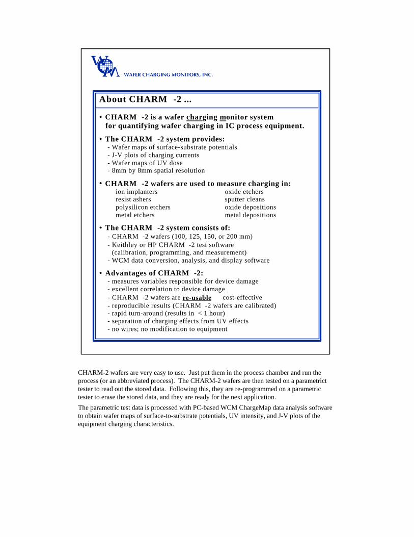
About CHARM -2 ...
•• CHARM-2 is a wafer charging monitor system for quantifying wafer charging in IC process equipment.
•• The CHARM-2 system provides:- Wafer maps of surface-substrate potentials- J-V plots of charging currents- Wafer maps of UV dose- 8mm by 8mm spatial resolution
•• CHARM-2 wafers are used to measure charging in:ion implantersresist asherspolysilicon etchersmetal etchers
oxide etcherssputter cleansoxide depositionsmetal depositions
•• The CHARM-2 system consists of:- CHARM-2 wafers (100, 125, 150, or 200 mm)- Keithley or HP CHARM-2 test software
(calibration, programming, and measurement)- WCM data conversion, analysis, and display software
•• Advantages of CHARM-2:- measures variables responsible for device damage- excellent correlation to device damage- CHARM-2 wafers are re-usable ⇒ cost-effective- reproducible results (CHARM-2 wafers are calibrated)- rapid turn-around (results in < 1 hour)- separation of charging effects from UV effects- no wires; no modification to equipment
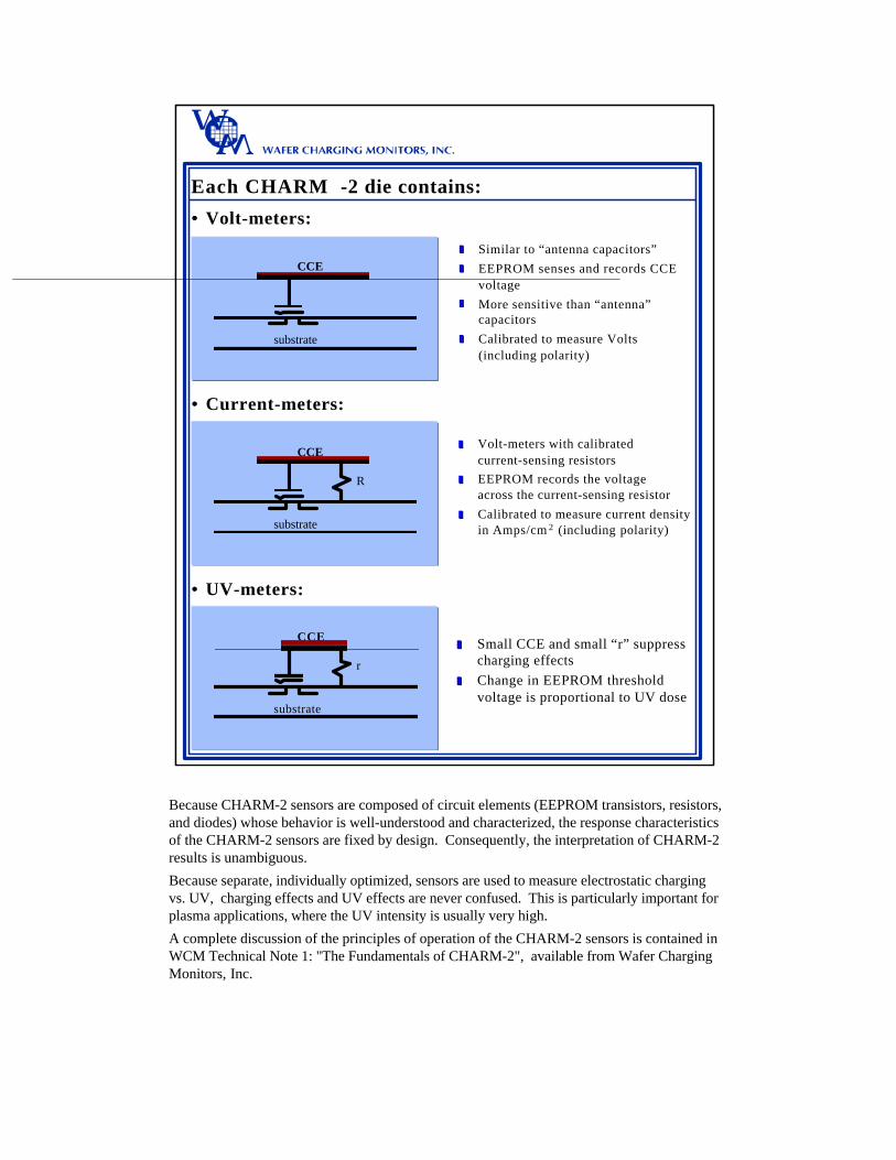
Because CHARM-2 sensors are composed of circuit elements (EEPROM transistors, resistors,and diodes) whose behavior is well-understood and characterized, the response characteristicsof the CHARM-2 sensors are fixed by design. Consequently, the interpretation of CHARM-2results is unambiguous.
Because separate, individually optimized, sensors are used to measure electrostatic chargingvs. UV, charging effects and UV effects are never confused. This is particularly important forplasma applications, where the UV intensity is usually very high.
A complete discussion of the principles of operation of the CHARM-2 sensors is contained inWCM Technical Note 1: "The Fundamentals of CHARM-2", available from Wafer ChargingMonitors, Inc.
Each CHARM-2 die contains:
•• Volt-meters:
substrate
CCEzz Analogous to “antenna capacitors”Similar to “antenna capacitors”
zz EEPROM senses and records CCEEEPROM senses and records CCEpotentialvoltage
zz More sensitive than “antenna”More sensitive than “antenna”capacitorscapacitors
zz Calibrated to measure potentialsCalibrated to measure Voltsin Volts (including polarity)(including polarity)
•• Current-meters:
substrate
R
CCEzz Potential sensors with calibratedVolt-meters with calibrated
current-sensing resistorscurrent-sensing resistors
zz EEPROM records the potentialEEPROM records the voltageacross the current-sensing resistoracross the current-sensing resistor
zz Calibrated to measure charge-fluxCalibrated to measure current densityin Amps/cmin Amps/cm 2 2 (including polarity)(including polarity)
•• UV-meters:
substrate
r
CCEzz Small CCE and small “r” suppressSmall CCE and small “r” suppress
charging effectscharging effects
zz Change in EEPROM thresholdChange in EEPROM thresholdvoltage is proportional to UV dosevoltage is proportional to UV dose
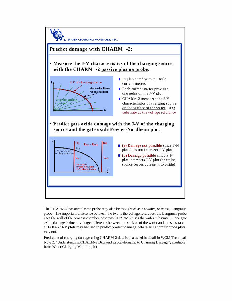
The CHARM-2 passive plasma probe may also be thought of as on-wafer, wireless, Langmuirprobe. The important difference between the two is the voltage reference: the Langmuir probeuses the wall of the process chamber, whereas CHARM-2 uses the wafer substrate. Since gateoxide damage is due to voltage difference between the surface of the wafer and the substrate,CHARM-2 J-V plots may be used to predict product damage, where as Langmuir probe plotsmay not.
Prediction of charging damage using CHARM-2 data is discussed in detail in WCM TechnicalNote 2: "Understanding CHARM-2 Data and its Relationship to Charging Damage", availablefrom Wafer Charging Monitors, Inc.
Predict damage with CHARM-2:
•• Measure the J-V characteristics of the charging source with the CHARM-2 passive plasma probe:
J
V
l
ll
l
l
l
l
J-V of charging source
piece-wise linearreconstruction
current-sensingresistor I-V
zz Implemented with multipleImplemented with multiplecharge-flux sensorscurrent-meters
zz Each sensor provides one pointEach current-meter provideson the J-V plotone point on the J-V plot
zz Measures the J-V characteristicsCHARM-2 measures the J-Vof charging source characteristics of charging source of the waferon the surface of the wafer using, , substrate as the voltage reference
•• Predict gate oxide damage with the J-V of the charging source and the gate oxide Fowler-Nordheim plot:
J
Gate oxideFowler-Nordheim(F-N) characteristic
tox1 tox2
tox1 < tox2
Jox
(a)(b)
J-V characteristicof charging source
V
zz (a) Damage not possible (a) Damage not possible since F-Nsince F-Nplot does not intersect J-V plotplot does not intersect J-V plot
zz (b) Damage possible (b) Damage possible since F-Nsince F-Nplot intersects J-V plot (chargingplot intersects J-V plot (chargingsource forces current into oxide)source forces current into oxide)
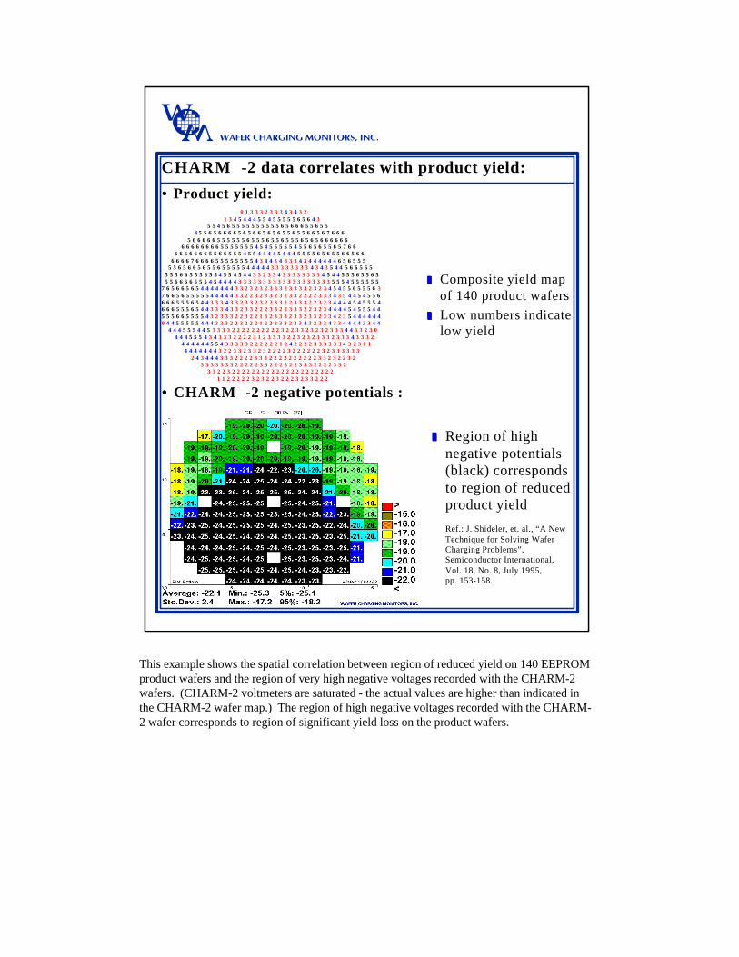
This example shows the spatial correlation between region of reduced yield on 140 EEPROMproduct wafers and the region of very high negative voltages recorded with the CHARM-2wafers. (CHARM-2 voltmeters are saturated - the actual values are higher than indicated inthe CHARM-2 wafer map.) The region of high negative voltages recorded with the CHARM-2 wafer corresponds to region of significant yield loss on the product wafers.
CHARM -2 data correlates with product yield:
•• Product yield:
zz Composite yield mapComposite yield mapof 140 product wafersof 140 product wafers
zz Low numbers indicateLow numbers indicatelow yieldlow yield
•• CHARM-2 negative potentials :
zz Region of highRegion of highnegative potentialsnegative potentials(black) corresponds(black) correspondsto region of reducedto region of reducedproduct yieldproduct yield
Ref.: J. Shideler, et. al., “A NewRef.: J. Shideler, et. al., “A NewTechnique for Solving WaferTechnique for Solving WaferCharging Problems”,Charging Problems”,Semiconductor International,Semiconductor International,Vol. 18, No. 8, July 1995,Vol. 18, No. 8, July 1995,pp. 153-158.pp. 153-158.
0 1 3 3 3 2 3 3 3 4 3 4 3 2 1 3 4 5 4 4 4 5 5 4 5 5 5 5 5 6 5 6 4 3
5 5 4 5 6 5 5 5 5 5 5 5 5 5 5 6 5 6 6 6 5 5 6 5 5 4 5 5 6 5 6 6 6 6 5 6 5 6 6 5 6 5 6 5 5 6 5 5 6 6 5 6 7 6 6 6 5 6 6 6 6 6 5 5 5 5 5 5 6 5 5 5 6 5 5 6 5 5 5 6 5 6 5 6 6 6 6 6 6 6 6 6 6 6 6 6 6 5 5 5 5 5 5 5 4 5 4 5 5 5 5 5 4 5 5 6 5 6 5 5 6 5 7 6 6 6 6 6 6 6 6 6 5 5 6 6 5 5 5 4 5 5 4 4 4 4 5 4 4 4 5 5 5 5 6 5 6 5 5 6 6 5 6 6 6 6 6 6 7 6 6 6 6 5 5 5 5 5 5 5 5 4 3 4 4 3 4 3 3 3 4 3 4 4 4 4 4 4 6 5 6 5 5 5 5 5 6 5 6 6 5 6 5 5 6 5 5 5 5 5 4 4 4 4 4 3 3 3 3 3 3 3 3 4 3 4 3 5 4 4 5 6 6 5 6 5 5 5 5 6 6 5 5 5 6 5 5 4 5 5 4 5 4 4 3 3 2 3 3 4 3 3 3 3 3 3 3 3 4 5 4 4 5 5 5 6 5 5 6 5 5 5 6 6 6 6 5 5 5 4 5 4 4 4 4 3 3 3 3 3 3 3 3 3 3 3 3 3 3 3 3 3 3 3 5 5 5 4 5 5 5 5 5 57 6 5 6 6 5 6 5 4 4 4 4 4 4 4 3 3 2 3 2 3 2 3 3 3 2 3 3 3 3 2 3 2 3 4 5 4 5 5 6 5 5 5 6 37 6 6 5 6 5 5 5 5 5 4 4 4 4 4 3 3 2 2 3 2 3 3 2 3 2 3 3 2 2 2 2 3 3 3 4 3 5 4 4 5 4 5 5 66 6 6 5 5 5 6 5 4 4 3 3 3 4 3 3 2 3 3 2 3 2 2 3 3 2 2 3 3 3 2 2 3 2 3 4 4 4 4 5 4 5 5 5 46 6 6 5 5 5 6 5 4 4 3 3 3 4 3 3 2 3 3 2 2 2 3 3 2 2 3 3 3 2 2 3 2 3 4 4 4 4 5 4 5 5 5 4 45 5 5 6 6 5 5 5 5 4 3 2 3 3 3 2 2 3 2 2 1 3 2 3 3 3 2 3 3 2 3 3 2 3 3 4 2 3 5 4 4 4 4 4 40 4 4 5 5 5 5 5 4 4 4 3 3 3 2 2 3 2 2 2 1 2 2 2 3 3 2 3 3 4 3 2 3 3 4 3 3 4 4 4 4 3 3 4 4 4 4 4 5 5 5 4 4 5 3 3 3 3 2 2 2 2 2 2 2 2 2 2 3 2 2 3 3 2 3 2 3 2 3 3 3 4 4 3 3 2 3 0 4 4 4 5 5 5 4 3 4 3 3 3 2 2 2 2 3 1 2 3 3 3 3 2 2 3 2 3 2 3 3 3 2 3 3 3 4 3 3 3 2 4 4 4 4 4 4 5 5 4 3 3 3 3 3 2 2 2 2 2 2 1 2 4 2 2 2 2 3 3 3 3 3 3 4 3 2 3 0 1 4 4 4 4 4 4 4 3 2 2 3 3 2 3 3 2 3 2 2 2 2 3 2 2 2 2 2 2 3 2 3 3 3 3 3 3 2 4 3 4 4 4 3 3 3 2 2 2 2 3 3 3 2 2 2 2 2 2 2 2 2 2 3 3 2 3 2 2 3 2 3 3 3 3 3 3 3 2 2 2 2 2 3 3 2 2 2 3 2 2 3 3 3 2 2 2 2 3 3 2 3 3 2 2 3 2 2 2 2 2 2 2 2 2 2 2 2 2 2 2 2 2 2 2 2 2 1 1 2 2 2 2 2 3 2 3 2 2 3 2 2 2 3 2 3 3 2 2 2
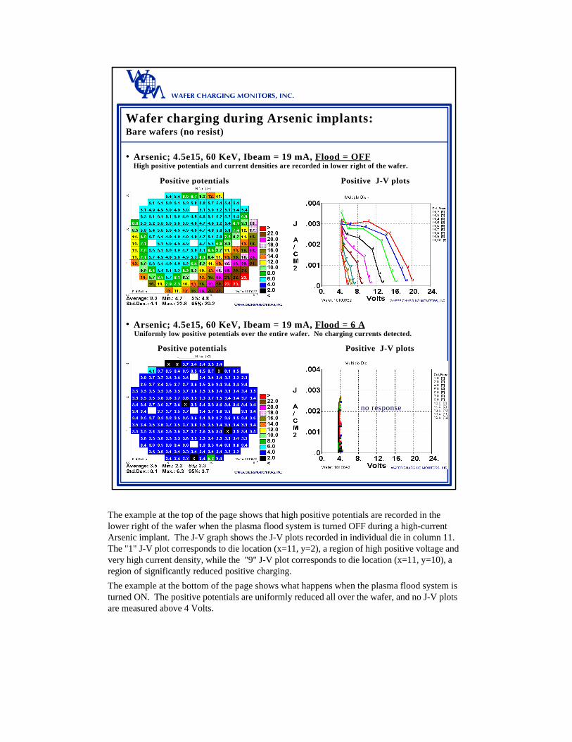
The example at the top of the page shows that high positive potentials are recorded in thelower right of the wafer when the plasma flood system is turned OFF during a high-currentArsenic implant. The J-V graph shows the J-V plots recorded in individual die in column 11.The "1" J-V plot corresponds to die location (x=11, y=2), a region of high positive voltage andvery high current density, while the "9" J-V plot corresponds to die location (x=11, y=10), aregion of significantly reduced positive charging.
The example at the bottom of the page shows what happens when the plasma flood system isturned ON. The positive potentials are uniformly reduced all over the wafer, and no J-V plotsare measured above 4 Volts.
Wafer charging during Arsenic implants:Bare wafers (no resist)
•• Arsenic; 4.5e15, 60 KeV, Ibeam = 19 mA, Flood = OFF High positive potentials and current densities are recorded in lower right of the wafer.
Positive potentials Positive J-V plots
•• Arsenic; 4.5e15, 60 KeV, Ibeam = 19 mA, Flood = 6 A Uniformly low positive potentials over the entire wafer. No charging currents detected.
Positive potentials Positive J-V plots
no response
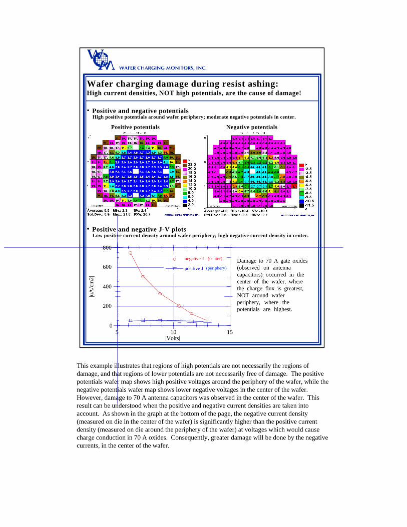
This example illustrates that regions of high potentials are not necessarily the regions ofdamage, and that regions of lower potentials are not necessarily free of damage. The positivepotentials wafer map shows high positive voltages around the periphery of the wafer, while thenegative potentials wafer map shows lower negative voltages in the center of the wafer.However, damage to 70 A antenna capacitors was observed in the center of the wafer. Thisresult can be understood when the positive and negative current densities are taken intoaccount. As shown in the graph at the bottom of the page, the negative current density(measured on die in the center of the wafer) is significantly higher than the positive currentdensity (measured on die around the periphery of the wafer) at voltages which would causecharge conduction in 70 A oxides. Consequently, greater damage will be done by the negativecurrents, in the center of the wafer.
Damage to 70 A gate oxides(observed on antennacapacitors) occurred in thecenter of the wafer, wherethe charge flux is greatest,NOT around waferperiphery, where thepotentials are highest.
0
200
400
600
800
|uA
/cm
2|
5 10 15|Volts|
negative J
positive J
(center)
(periphery)
Wafer charging damage during resist ashing:High current densities, NOT high potentials, are the cause of damage!
•• Positive and negative potentials High positive potentials around wafer periphery; moderate negative potentials in center.
Positive potentials Negative potentials
•• Positive and negative J-V plots Low positive current density around wafer periphery; high negative current density in center.
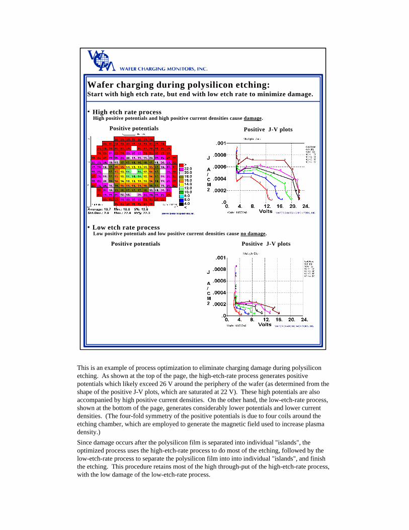
This is an example of process optimization to eliminate charging damage during polysiliconetching. As shown at the top of the page, the high-etch-rate process generates positivepotentials which likely exceed 26 V around the periphery of the wafer (as determined from theshape of the positive J-V plots, which are saturated at 22 V). These high potentials are alsoaccompanied by high positive current densities. On the other hand, the low-etch-rate process,shown at the bottom of the page, generates considerably lower potentials and lower currentdensities. (The four-fold symmetry of the positive potentials is due to four coils around theetching chamber, which are employed to generate the magnetic field used to increase plasmadensity.)
Since damage occurs after the polysilicon film is separated into individual "islands", theoptimized process uses the high-etch-rate process to do most of the etching, followed by thelow-etch-rate process to separate the polysilicon film into into individual "islands", and finishthe etching. This procedure retains most of the high through-put of the high-etch-rate process,with the low damage of the low-etch-rate process.
Wafer charging during polysilicon etching:Start with high etch rate, but end with low etch rate to minimize damage.
•• High etch rate process High positive potentials and high positive current densities cause damage.
Positive potentials Positive J-V plots
•• Low etch rate process Low positive potentials and low positive current densities cause no damage.
Positive potentials Positive J-V plots
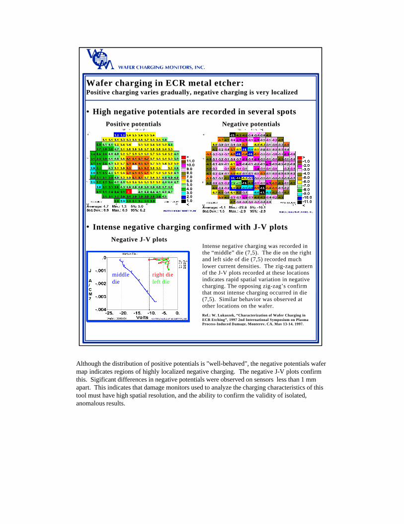
Although the distribution of positive potentials is "well-behaved", the negative potentials wafermap indicates regions of highly localized negative charging. The negative J-V plots confirmthis. Sigificant differences in negative potentials were observed on sensors less than 1 mmapart. This indicates that damage monitors used to analyze the charging characteristics of thistool must have high spatial resolution, and the ability to confirm the validity of isolated,anomalous results.
Wafer charging in ECR metal etcher:Positive charging varies gradually, negative charging is very localized
•• High negative potentials are recorded in several spots
Positive potentials Negative potentials
•• Intense negative charging confirmed with J-V plots
Negative J-V plots
middledie
right dieleft die
Intense negative charging was recorded inthe “middle” die (7,5). The die on the rightand left side of die (7,5) recorded muchlower current densities. The zig-zag patternof the J-V plots recorded at these locationsindicates rapid spatial variation in negativecharging. The opposing zig-zag’s confirmthat most intense charging occurred in die(7,5). Similar behavior was observed atother locations on the wafer.
Ref.: W. Lukaszek, “Characterization of Wafer Charging inECR Etching”, 1997 2nd International Symposium on PlasmaProcess-Induced Damage, Monterey, CA, May 13-14, 1997.
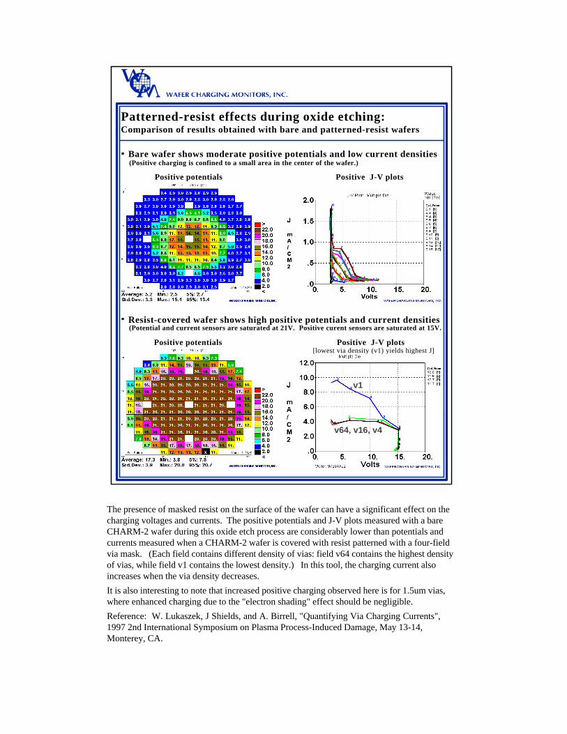
The presence of masked resist on the surface of the wafer can have a significant effect on thecharging voltages and currents. The positive potentials and J-V plots measured with a bareCHARM-2 wafer during this oxide etch process are considerably lower than potentials andcurrents measured when a CHARM-2 wafer is covered with resist patterned with a four-fieldvia mask. (Each field contains different density of vias: field v64 contains the highest densityof vias, while field v1 contains the lowest density.) In this tool, the charging current alsoincreases when the via density decreases.
It is also interesting to note that increased positive charging observed here is for 1.5um vias,where enhanced charging due to the "electron shading" effect should be negligible.
Reference: W. Lukaszek, J Shields, and A. Birrell, "Quantifying Via Charging Currents",1997 2nd International Symposium on Plasma Process-Induced Damage, May 13-14,Monterey, CA.
Patterned-resist effects during oxide etching:Comparison of results obtained with bare and patterned-resist wafers
•• Bare wafer shows moderate positive potentials and low current densities (Positive charging is confined to a small area in the center of the wafer.)
Positive potentials Positive J-V plots
•• Resist-covered wafer shows high positive potentials and current densities (Potential and current sensors are saturated at 21V. Positive curent sensors are saturated at 15V.)
Positive potentials Positive J-V plots [lowest via density (v1) yields highest J]
v1
v64, v16, v4
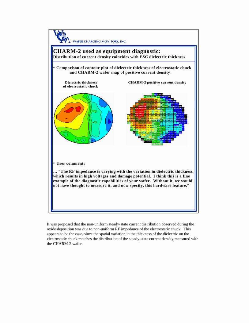
It was proposed that the non-uniform steady-state current distribution observed during theoxide deposition was due to non-uniform RF impedance of the electrostatic chuck. Thisappears to be the case, since the spatial variation in the thickness of the dielectric on theelectrostatic chuck matches the distribution of the steady-state current density measured withthe CHARM-2 wafer.
CHARM-2 used as equipment diagnostic:Distribution of current density coincides with ESC dielectric thickness
•• Comparison of contour plot of dielectric thickness of electrostatic chuck and CHARM-2 wafer map of positive current density
Dielectric thicknessof electrostatic chuck
CHARM-2 positive current density
•• User comment:
… “The RF impedance is varying with the variation in dielectric thicknesswhich results in high voltages and damage potential. I think this is a fineexample of the diagnostic capabilities of your wafer. Without it, we wouldnot have thought to measure it, and now specify, this hardware feature.”
Application of CHARM-2 monitors:
•• CHARM-2 monitors have been used for:
ü new equipment selectionü equipment acceptance testsü equipment calibrationü equipment benchmarkingü equipment problem diagnosisü new equipment developmentü identifying equipment responsible for yield lossü process optimizationü maintenance schedulingü studies of basic charging mechanismsü studies of photoresist-mediated wafer chargingü UV lamp qualification