Embed Size (px)
Citation preview

User Manual
TR 210 Tracker
071-0114-01

Copyright Tektronix, Inc. All rights reserved.
Tektronix products are covered by U.S. and foreign patents, issued and pending. Information in this publication supercedesthat in all previously published material. Specifications and price change privileges reserved.
Printed in the U.S.A.
Tektronix, Inc., PO Box 500, Beaverton, OR 97077
TEKTRONIX and TEK are registered trademarks of Tektronix, Inc.
Huntron and Tracker are registered trademarks of Huntron, Inc.

WARRANTY
Tektronix warrants that the products that it manufactures and sells will be free from defects in materials andworkmanship for a period of one (1) year from the date of purchase from an authorized Tektronix distributor. Ifany such product proves defective during this warranty period, Tektronix, at its option, either will repair thedefective product without charge for parts and labor, or will provide a replacement in exchange for the defectiveproduct. Batteries are excluded from this warranty.
In order to obtain service under this warranty, Customer must notify Tektronix of the defect before the expirationof the warranty period and make suitable arrangements for the performance of service. Customer shall beresponsible for packaging and shipping the defective product to the service center designated by Tektronix,shipping charges prepaid, and with a copy of customer proof of purchase. Tektronix shall pay for the return of theproduct to Customer if the shipment is to a location within the country in which the Tektronix service center islocated. Customer shall be responsible for paying all shipping charges, duties, taxes, and any other charges forproducts returned to any other locations.
This warranty shall not apply to any defect, failure or damage caused by improper use or improper or inadequatemaintenance and care. Tektronix shall not be obligated to furnish service under this warranty a) to repair damageresulting from attempts by personnel other than Tektronix representatives to install, repair or service the product;b) to repair damage resulting from improper use or connection to incompatible equipment; c) to repair anydamage or malfunction caused by the use of non-Tektronix supplies; or d) to service a product that has beenmodified or integrated with other products when the effect of such modification or integration increases the timeor difficulty of servicing the product.
THIS WARRANTY IS GIVEN BY TEKTRONIX WITH RESPECT TO THE LISTED PRODUCTS INLIEU OF ANY OTHER WARRANTIES, EXPRESS OR IMPLIED. TEKTRONIX AND ITS VENDORSDISCLAIM ANY IMPLIED WARRANTIES OF MERCHANTABILITY OR FITNESS FOR APARTICULAR PURPOSE. TEKTRONIX’ RESPONSIBILITY TO REPAIR OR REPLACE DEFECTIVEPRODUCTS IS THE SOLE AND EXCLUSIVE REMEDY PROVIDED TO THE CUSTOMER FORBREACH OF THIS WARRANTY. TEKTRONIX AND ITS VENDORS WILL NOT BE LIABLE FOR ANYINDIRECT, SPECIAL, INCIDENTAL, OR CONSEQUENTIAL DAMAGES IRRESPECTIVE OFWHETHER TEKTRONIX OR THE VENDOR HAS ADVANCE NOTICE OF THE POSSIBILITY OFSUCH DAMAGES.

Contacting Tektronix
ProductSupport
For application-oriented questions about a Tektronix measure-ment product, call toll free in North America:1-800-TEK-WIDE (1-800-835-9433 ext. 2400)6:00 a.m. – 5:00 p.m. Pacific time
Or contact us by e-mail:[email protected]
For product support outside of North America, contact yourlocal Tektronix distributor or sales office.
ServiceSupport
Contact your local Tektronix distributor or sales office. Or visitour web site for a listing of worldwide service locations.
http://www.tek.com
For otherinformation
In North America:1-800-TEK-WIDE (1-800-835-9433)An operator will direct your call.
To write us Tektronix, Inc.P.O. Box 500Beaverton, OR 97077

TR 210 User Manual i
Contents
General Safety Summary................................................................................ v
Introduction and Specifications .................................................................. 1-1What is Signature Analysis?........................................................................... 1-2Power Configuration ...................................................................................... 1-3Signal Fuse Replacement................................................................................ 1-450/60Hz Selector Switch ................................................................................ 1-4Unpacking Your TR 210 ................................................................................ 1-4Installation ...................................................................................................... 1-5Operating the TR 210 ..................................................................................... 1-6Specifications ................................................................................................. 1-8Accessories ..................................................................................................... 1-12
A Quick Tour ................................................................................................ 2-1Front Panel...................................................................................................... 2-2Back Panel ...................................................................................................... 2-4Oscilloscope Display ...................................................................................... 2-5Initial Setups................................................................................................... 2-6Power On ........................................................................................................ 2-6Range Selection .............................................................................................. 2-6Frequency Selection ....................................................................................... 2-7Channel Selection........................................................................................... 2-7Pulse Generator .............................................................................................. 2-8
Using Your TR 210....................................................................................... 3-1Basics of ASA - How it Works ...................................................................... 3-2Horizontal Axis .............................................................................................. 3-3Vertical Axis................................................................................................... 3-4Basic Analog Signatures - Open and Short .................................................... 3-5Four Basic Component Analog Signatures .................................................... 3-7

Contents
ii TR 210 User Manual
Testing Passive Components........................................................................ 4-1Resistors.......................................................................................................... 4-1Shorts and Opens, Resistor Faults .................................................................. 4-4Review ............................................................................................................ 4-4Troubleshooting Applications ........................................................................ 4-5Capacitors ....................................................................................................... 4-6Capacitor Analog Signatures .......................................................................... 4-7The Signatures of Different Capacitors in LOW2 Range............................... 4-8Understanding Capacitor Analog Signatures.................................................. 4-9Capacitor Failures - Leakage .......................................................................... 4-10Review ............................................................................................................ 4-11Applications.................................................................................................... 4-11Inductors ......................................................................................................... 4-11Inductor Analog Signatures ............................................................................ 4-12The Signatures of Different Inductors in LOW2 Range................................. 4-13Affect of Frequency Fs on Inductor Signatures .............................................. 4-13Understanding Inductive Signatures............................................................... 4-14Review ............................................................................................................ 4-14Applications.................................................................................................... 4-15Electromechanical Switching Components .................................................... 4-16Manually Operated Mechanical Switches ...................................................... 4-16Review ............................................................................................................ 4-18Electomechanical Relays ................................................................................ 4-18Relay Coil Test ............................................................................................... 4-18Using the Pulse Generator to Test a 5V Reed Relay...................................... 4-19Review ............................................................................................................ 4-20
Testing Discrete Semiconductors ................................................................ 5-1Diodes ............................................................................................................. 5-1Diode Analog Signatures ................................................................................ 5-1Affects of Frequency (Fs) on the Diode Signature ......................................... 5-3The Composite Diode Signature..................................................................... 5-3Diode Failures................................................................................................. 5-4Internal Resistance Flaw in a Diode ............................................................... 5-5Internal Leakage Flaw in a Diode................................................................... 5-6Zener Diodes................................................................................................... 5-6Review ............................................................................................................ 5-8Applications.................................................................................................... 5-8Transistors ...................................................................................................... 5-9Bipolar Transistor Signatures ......................................................................... 5-9Bipolar Transistor Base-Collector Signatures ................................................ 5-10Identifying Unknown Transistors ................................................................... 5-12Darlington Bipolar Transistor Signatures....................................................... 5-14Using the Pulse Generator to Test Transistor Operation................................ 5-15Analyzing the Active Characteristics of a Transistor..................................... 5-16Review ............................................................................................................ 5-17Applications.................................................................................................... 5-18Optical Switches ............................................................................................. 5-18Phototransistors .............................................................................................. 5-19

Contents
TR 210 User Manual iii
Optocoupler Dynamic Testing........................................................................ 5-20Optocoupler Signatures .................................................................................. 5-20SCRs and Triacs ............................................................................................. 5-22Silicon Controlled Rectifiers (SCRs) ............................................................. 5-22Active Testing of an SCR............................................................................... 5-24Triacs .............................................................................................................. 5-25Active Testing of Triacs ................................................................................. 5-26Review............................................................................................................ 5-27Applications.................................................................................................... 5-27
Testing Integrated Circuits.......................................................................... 6-1Digital Integrated Circuits .............................................................................. 6-1Integrated Circuit Failures.............................................................................. 6-1Digital Integrated Circuit Signatures.............................................................. 6-2Signatures of a Digital IC ............................................................................... 6-3Signatures for Different Logic Chip Families ................................................ 6-4Comparing Two TTL Families....................................................................... 6-4CMOS Logic Family ...................................................................................... 6-5CMOS Components and Test Signal Frequency Fs........................................ 6-7Troubleshooting Digital Logic ICs................................................................. 6-8Comparison Testing for Digital ICs ............................................................... 6-9Review............................................................................................................ 6-10Applications.................................................................................................... 6-10Analog Circuits............................................................................................... 6-11Op Amps......................................................................................................... 6-11Op Amp Signatures ........................................................................................ 6-12Troubleshooting Op Amp Circuits ................................................................. 6-13Linear Voltage Regulators.............................................................................. 6-14Review............................................................................................................ 6-15Applications.................................................................................................... 6-15Low Voltage ................................................................................................... 6-16Review............................................................................................................ 6-18Applications.................................................................................................... 6-18

Contents
iv TR 210 User Manual

TR 210 User Manual v
General Safety Summary
Review the following safety precautions to avoid injury and prevent damage tothis product or any products connected to it. To avoid potential hazards, use thisproduct only as specified.
Only qualified personnel should perform service procedures.
To Avoid Fire or PersonalInjury
Use Proper Power Cord. Use only the power cord specified for this product andcertified for the country of use.
Use Proper Voltage Setting. Before applying power, ensure that the line selector isin the proper position for the power source being used.
Connect and Disconnect Properly. Do not connect or disconnect probes or test leadswhile they are connected to a voltage source.
Ground the Product. This product is grounded through the grounding conductor ofthe power cord. To avoid electric shock, the grounding conductor must beconnected to earth ground. Before making connections to the input or outputterminals of the product, ensure that the product is properly grounded.
Observe All Terminal Ratings. To avoid fire or shock hazard, observe all ratings andmarkings on the product. Consult the product manual for further ratingsinformation before making connections to the product.
Do not apply a potential to any terminal, including the common terminal, thatexceeds the maximum rating of that terminal.
Do Not Operate Without Covers. Do not operate this product with covers or panelsremoved.
Use Proper Fuse. Use only the fuse type and rating specified for this product.
Avoid Exposed Circuitry. Do not touch exposed connections and components whenpower is present.
Do Not Operate With Suspected Failures. If you suspect there is damage to thisproduct, have it inspected by qualified service personnel.
Do Not Operate in Wet/Damp Conditions.
Do Not Operate in an Explosive Atmosphere.
Keep Product Surfaces Clean and Dry.

General Safety Summary
vi TR 210 User Manual
Symbols and Terms Terms in this Manual. These terms may appear in this manual:
WARNING. Warning statements identify conditions or practices that could result ininjury or loss of life.
CAUTION. Caution statements identify conditions or practices that could result indamage to this product or other property.
Terms on the Product. These terms may appear on the product:
DANGER indicates an injury hazard immediately accessible as you read themarking.
WARNING indicates an injury hazard not immediately accessible as you readthe marking.
CAUTION indicates a hazard to property including the product.
Symbols on the Product. The following symbols may appear on the product:

TR 210 User Manual 1-1
Introduction and Specifications
The Tektronix TR 210 is an accessory to an oscilloscope which allows power offtroubleshooting of electronic circuits by using the technique of Analog SignatureAnalysis.
This signature shows the V/I characteristics of an electronic device which whencompared with a known good device, can assist in locating faulty components ofa circuit without applying power to the board under test. This technique oftroubleshooting simply involves the visual comparison of circuit signatureswhich can assist in isolating circuit failures due to opens, shorts, device leakage,ESD damage, power supply over-voltage and transients.
Figure 1-1. TR 210
Introduction and Specifications
1-2 TR 210 User Manual
What is Analog Signature Analysis?
Analog Signature Analysis or ASA is a unique, power-off troubleshootingtechnique. It uses an alternating current (AC) sinewave stimulus to show thecurrent (I) vs. voltage (V) characteristic of an unpowered component on a CRT.The IV characteristic is called an analog signature and each pin of a componentcan have a unique signature. When components fail, their signatures change sotroubleshooting using ASA is simply a matter of finding the defectivecomponent by analyzing its signature. You can compare signatures of suspectcomponents to signatures of known-good components.
Test current applied across a component is limited. When used carefully, thistechnique is non-destructive and does not damage any components. ASA hasmany advantages as a proven, fast, and effective troubleshooting technique.
You can:
Troubleshoot circuitry that cannot be powered up due to a shorted condition.
Troubleshoot in a qualitative mode, allowing you to see physical problemswith a suspect component.
Compare device characteristics with known types for better matching.
Eliminate risk of accidental shorting across other points during POWER ONtesting which could further damage the component or other components onthe board.
Minimize the risk of shock hazard since the ASA troubleshooting approachrequires no power applied to the circuitry.
Perform preventative maintenance by seeing flaws in components that couldpossibly lead to untimely failures.
Look at replacement components before they are installed in circuitry toreduce the risk of installing defective ones.

Introduction and Specifications
TR 210 User Manual 1-3
The Tektronix TR 210 graphically displays the analog signature when connectedto two terminals of a component for visual interpretation. ASA may beuniversally applied to any type of passive component like a resistor, capacitor, orinductor, or a solid state semiconductor component like a diode, transistor, SCR,digital, analog, or mixed-signal IC. When troubleshooting a board, the resultantsignature is a composite of various component signatures at a particular node inthe circuitry. By understanding what different signatures mean, you candetermine which components are faulty.
Power Configuration
CAUTION. To avoid product damage, set the line selector switch to the correctposition and install the correct fuse before applying line power.
Line Selector Switch The Line Selector Switch, located on the TR 210’s back panel, selects between100/115VAC and 230VAC. Slide the switch to the line voltage that you will beusing.
Line Fuse The power entry module on the TR 210 includes the power switch (0 = OFF,1 = ON), power cord connector, and a removable tray which holds the line fuseand a spare fuse. Make sure that replacement fuses are of the type and currentrating specified. If necessary, insert the specified line fuse (see line fusespecification on page 1-9) into the fuse tray.
Figure 1-2. Back panel.
The line fuse should only open when there is a failure inside the instrument.Therefore the problem should always be located and corrected before fusereplacement. Be sure to always use a fuse with the type and rating specified onpage 1-9.

Introduction and Specifications
1-4 TR 210 User Manual
Signal Fuse Replacement
The Signal fuse is located on the back panel of the TR 210 in a panel mountedfuse holder. If the fuse opens, replace it with another 5 mm x 20 mm, F250 mA250 V (IEC127-2/II type GDB) fuse.
50/60Hz Selector Switch
The 50/60Hz Selector Switch, located on the TR 210 back panel, is forindicating to the TR 210 what your line frequency is. Slide the switch to thesetting that matches your line frequency.
Unpacking Your TR 210
Your instrument was shipped with the following items:
Table 1-2. TR 210 Shipping and Replaceable Parts List
Part Number Description Quantity
ATL25 Tracker Probes 1 pair
98-0043* Black Ground Leads 2
98-0270* Blue Clip Leads 2
161-0230-01 Power Cord (115V) † 1
071-0114-XX TR 210 User Manual † 1* Replacements available from Huntron, Inc. See page 1-12 for ordering information.† Options add international power cords and translated manuals.
Check the shipment carefully and contact the place of purchase if anything ismissing. If there is shipping damage, then contact your freight company. Ifshipment is necessary, please use the original shipping carton and packing foam.If these are not available, be sure that the instrument is packed in a box with aminimum of two inches (5 cm) of cushioning material on all sides.

Introduction and Specifications
TR 210 User Manual 1-5
Installation
The TR 210 requires a 2 channel Oscilloscope with X/Y capability fordisplaying the signature of the device under test.
1. The figure below shows a typical connection of a TR 210 to anoscilloscope.
Figure 1-3. Typical TR 210-to-Oscilloscope connection.
2. Using BNC cables, connect the first oscilloscope channel 1 or X to theHorizontal (X) channel of the TR 210. Connect the second oscilloscopechannel 2 or Y to the Vertical (Y) channel of the TR 210.
3. Connect the power cord to the TR 210 and switch the unit on.

Introduction and Specifications
1-6 TR 210 User Manual
4. Setup the oscilloscope as follows:
1 V/div vertical scale on each channel5 ms/div time base
Trigger on channel 1 X/Y mode
The TR 210 will be in the LOW2 range. Adjust the Horizontal position sothat the open circuit trace which should be a horizontal line is at thehorizontal crosshair of the graticule. Connect the test probes to the frontpanel A and COM terminals of the TR 210. Short the test terminals. Avertical Trace will be displayed. Adjust the vertical position of the trace sothat it is at the vertical crosshair of the graticule.
5. You are now ready to use the TR 210.
Operating the TR 210
1. To select a test range, press one of the five range buttons.
2. To select a test frequency, press one of the three frequency buttons. All testranges will then be using the selected frequency.
3. To compare two devices, connect the test terminal of channel A to thereference or good device. Plug the banana jack of a second test probe to thechannel B test terminal. See Figure 1-4 for instructions on adjusting theprobe tips. Connect the test probe to the suspect device. Connect thecommon lead to one of the COM terminals. Press the ALT button and set thespeed at which channel A and B will switch by turning the RATE knob. Thesignature of Channel A will alternate with the signature of channel B for aneasy visual comparison of the two signatures.

Introduction and Specifications
TR 210 User Manual 1-7
Figure 1-4. Adjusting the Probe Tips.
4. To avoid pressing each one of the test ranges, press the SCAN button. Thiswill scan through all the test ranges one at a time.
5. The pulse generator is used to test gate fired devices like SCRs and Triacs.By connecting the G1 terminal to the gate of the device and applying the testterminal across the anode and cathode of the device, it is possible to actuallyturn the device on and look at the V/I characteristics of the device. This isparticularly useful for power supplies where you are unable to turn ondevices because the power supply is faulty on power up.
6. Refer to later chapters of this manual for details on testing resistors,capacitors, inductors, diodes, multiple component circuits, integratedcircuits, SCRs and optocouplers.

Introduction and Specifications
1-8 TR 210 User Manual
Specifications
The specifications for the TR 210 are listed in Table 1-1.
Table 1-1. TR 210 Specifications
Electrical
Test Signal: Sine wave
Open Circuit Voltage (VS): 60 Vpk HIGH Range
20 Vpk MED 2 Range
15 Vpk MED 1 Range
10 Vpk LOW 2 Range
3 Vpk LOW 1 Range
Source Resistance (RS): 74 kΩ HIGH Range
27.6 kΩ MED 2 Range
1.24 kΩ MED 1 Range
54 Ω LOW 2 Range
10 kΩ LOW 1 Range
Frequency (FS): 50/60 Hz
200 Hz
2000 Hz
Channels:
Number 2
Display modes A, B, Alt
Overload Protection Fuse: 5 mm x 20 mm, F250 mA, 250 V(IEC 127-2/II, type GDB)
Overvoltage Category CAT I
Pulse Generator:
Number of Outputs: 2
Level 0 V to +/- 5 V, open circuit
DC Mode +/- DC Level
Pulse Mode +/- or Composite
Frequency Matches selected test signal frequency
Width (pulse mode) 2% to 50% duty cycle
Source resistance 100 Ω each output
Short circuit current 50 mA max. each output
Introduction and Specifications
TR 210 User Manual 1-9
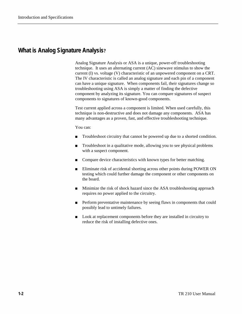
Table 1-1. TR 210 Specifications (continued)
Electrical (continued):
Power Requirements:
Line Voltage 100/115 VAC or 230 VAC
Frequency 50 Hz to 60 Hz
Power 15 W maximum
Line Fuse 100/115 V: 5 mm x 20 mm, T160 mA, 250 V(IEC127-2/III, type GDC)
230 V: 5 mm x 20 mm, T160 mA, 250 V(IEC127-2/III, type GDC)
Mechanical
Dimensions 11.5” W x 2.7” H x 10.2” D(29.1 cm W x 6.9 cm H x 25.9 cm D)
Weight 4.6 lbs (2.1 kg)
Shipping Weight approx. 7 lbs (3.0 kg)
Environmental
Indoor Use
Altitude <2000m (<6560')
Temperature
Operating 0°C to +40°C (32°F to 104°F)
Storage -50°C to +60°C (-58°F to 140°F)
Relative Humidity < 80% up to 31°C,derated linearly to 50% at 40°C

Introduction and Specifications
1-10 TR 210 User Manual
Table 1-1. TR 210 Specifications (continued)
Certifications and Compliances
EC Declaration of Conformity - EMC Directive Meets the intent of Directive 89/336/EC forElectromagnetic Compatibility. Compliancewas demonstrated to the followingspecifications as listed in the Official Journal ofthe European Communities:
EN 50081-1 Emissions:EN 55011 Class B Radiated and
Conducted EmissionsEN 50082-1 Immunity:
IEC1000-4-2 Electrostatic DischargeIEC1000-4-3 RF Electromagnetic
FieldIEC1000-4-4 Electrical Fast Transient/
BurstIEC1000-4-5 Power Line Surge
EC Declaration of Conformity - Low VoltageDirective
Compliance was demonstrated to the followingspecification as listed in the Official Journal ofthe European Communities:
Low Voltage Directive 73/23/EEC, asammended by 93/68/EEC
EN 61010-1:1993Safety requirements for electricalequipment for measurement,control, and laboratory use

Introduction and Specifications
TR 210 User Manual 1-11
Table 1-1. TR 210 Specifications (continued)
Certifications and Compliances (continued)
Approvals UL3111-1 Standard for electrical measuringand test equipment
CAN/CSA C22.2 No. 1010.1 Safetyrequirements for electrical equipment formeasurement, control, and laboratory use
Installation Category Descriptions Terminals on this product may have differentcategory designations. The installationcategories are:
CAT III - Distribution-level mains (usuallypermanently connected). Equipment at thislevel is typically in a fixed industrial location.
CAT II - Local-level mains (wall sockets).Equipment at this level includes appliances,portable tools, and similar products. Equipmentis usually cord connected.
CAT I - Secondary (signal level) or batteryoperated circuits of electronic equipment.
Pollution Degree 2
NOTE. Tektronix does not offer a Certificate of Traceable Calibration for theTR 210. The TR 210 is a troubleshooting tool and is not intended for use incalibration or conformance-testing applications.
Introduction and Specifications
1-12 TR 210 User Manual
Accessories
You can order a foot switch (part number 98-0314) and other replacement partsfrom Huntron, Inc., at the address below:
Huntron, Inc.15720 Mill Creek Blvd.Mill Creek, WA 98012 U.S.A.phone: 425-743-3171, or 1-800-426-9265 in the U.S.A.
The foot switch connects to the back panel of the TR 210. When the switch isdepressed, the next test range is automatically selected. Using the foot switch is aconvenient way of avoiding having to manually select the test range on theTR 210 front panel.

TR 210 User Manual 2-1
A Quick Tour
The Tektronix TR 210 is a versatile troubleshooting tool having the followingfeatures:
Four test ranges and an additional low voltage (3 Volt) range for Low PowerSurface Mounted devices.
Two-channel pulse generator allowing the testing of gate fired devices.
Three test frequencies to expand the range capability for testing capacitorsand inductors.
Two-channel compairson mode allowing the automatic switching betweenthe reference signature and the suspect signature.
Easy hookup to an oscilloscope with X/Y capability for displaying thesignatures.
The TR 210 tests components using a two terminal system (three terminalsystem when the built-in pulse generator is used) where two leads are placed onthe leads of the component under test. The TR 210 tests components in-circuit,even when there are several components in parallel.
All voltage sources in boards and systems must be in a power-off condition whenusing the TR 210. Electronic protection is a signal fuse connected in series withthe channel A and B test terminals. Accidental contact of the test leads to activevoltage sources, for example, line voltage, powered-up boards or systems,charged high voltage capacitors, etc., may cause the signal fuse to open. Anopen signal fuse is indicated by channel A and B showing a short-circuitsignature at all times regardless if anything is connected across the probes.When this condition occurs, follow the directions in Signal Fuse Replacement onpage 1-4 for replacing the signal fuse.
CAUTION. The device to be tested must have all power turned off, and have allhigh voltage capacitors discharged before connecting the TR 210 to the device.
A Quick Tour
2-2 TR 210 User Manual
Before you begin to use the TR 210, please take a few minutes to familiarizeyourself with the instrument. All of the externally accessible features arediscussed in the following sections.
Front Panel
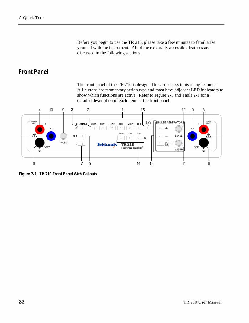
The front panel of the TR 210 is designed to ease access to its many features.All buttons are momentary action type and most have adjacent LED indicators toshow which functions are active. Refer to Figure 2-1 and Table 2-1 for adetailed description of each item on the front panel.
Figure 2-1. TR 210 Front Panel With Callouts.
A Quick Tour
TR 210 User Manual 2-3
Table 2-1. Front Panel Controls And Connections.
Name Function
1 Range Selectors Push buttons that select one of five impedanceranges: LOW1, LOW2, MED1, MED2 and HIGH
2 Scan Switch Push button that initiates automatic scanning of thefive ranges from LOW1 to HIGH. The scanningspeed is determined by the RATE control (see item#9).
3 Channel A Switch Selects channel A for display on the oscilloscope.
4 Channel A Test Terminal Safety shrouded banana jack for channel A testsignal.
5 ALT Switch Causes the TR 210 to alternate between channel Aand channel B at a speed determined by the RATEcontrol (see item #9).
6 COM Test Terminal Safety shrouded banana jack that is the instrumentcommon and the common reference point for bothchannel A and channel B.
7 Channel B Switch Selects channel B for display on the oscilloscope.
8 Channel B Test Terminal Safety shrouded banana jack for channel B testsignal.
9 RATE Control Controls the speed of channel alternation and/orrange scanning.
10 G1 & G2 Terminals Pulse Generator dual outputs.
11 WIDTH Control Controls the duty cycle of the pulse generator output.
12 LEVEL Control Controls the amplitude of the pulse generator output.
13 Pulse Generator Selectors Push buttons that select various output modes of thepulse generator: Positive(+), Negative (-) andPULSE/DC.
14 Frequency Selectors Push buttons that select one of the three signalfrequencies: 50/60 Hz, 200 Hz and 2000 Hz.
15 NO HIGH range Switch Push button that activates a mode where it is notpossible to enter the HIGH range either by manual orscan range selection.

A Quick Tour
2-4 TR 210 User Manual
Back Panel
Secondary controls and connectors are on the back panel. Refer to Figure 2-2and Table 2-2 for a detailed description of each item on the back panel
Figure 2-2. TR 210 Back Panel.
Table 2-2. Back Panel Connections.
Name Function
1 Input Voltage Selector Select between 100/115 VAC and 230 VAC inputvoltage.
2 Power cord connectorPower fuse holderPower switch
IEC standard connector that mates with any CDD-22power cord. Power fuse holder and Power switch.
3 X & Y output X & Y outputs connects to oscilloscope.
4 Input Hz selector Select between 50 or 60 Hz input frequency
5 Remote Switch Using the Foot Switch accessory, you can change tothe next range in the scan sequence.
6 Signal Fuse 250 mA fuse.
A Quick Tour
TR 210 User Manual 2-5
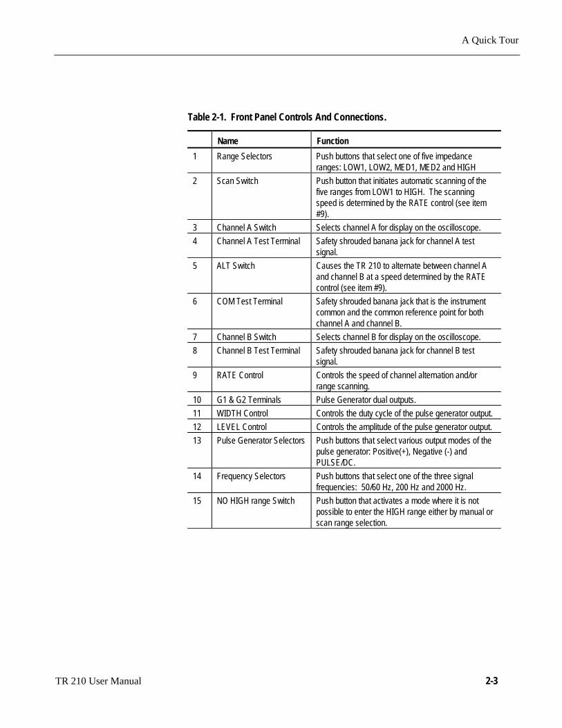
Oscilloscope Display
The TR 210 uses the display of any oscilloscope that is capable of displaying anuntriggered XY waveform. The oscilloscope display can be divided into fourquadrants. Each quadrant displays different portions of the signatures. Quadrant1 displays positive voltage (+V) and positive current (+I), quadrant 2 displaysnegative voltage (-V) and positive current (+I), quadrant 3 displays negativevoltage (-V) and negative current (-I), and quadrant 4 displays positive voltage(+V) and negative current (-I).
Figure 2-3. Oscilloscope Display.

A Quick Tour
2-6 TR 210 User Manual
Initial Setups
The following setups assume that the TR 210 has been connected to anoscilloscope and the TR 210s power cord has been plugged into an appropriatewall socket.
Power On
Turn the power on to your TR 210 using the power switch located on the rearpanel. The TR 210 should come on with the LEDs for channel A, 50/60 Hz,LOW2 range and Pulse/DC illuminated.
Range Selection
The TR 210 is designed with five impedance ranges (LOW1, LOW2, MED1,MED2 and HIGH). These ranges are selected by pressing the appropriate buttonon the front panel. It is best to start with one of the medium ranges (i.e. MED1or MED2). If the signature on the oscilloscope display is close to an open(horizontal trace), go to the next higher range for a more descriptive signature. Ifthe signature is close to a short (vertical trace), go to the next lower range.
NOTE: In HIGH range, up to 60 Vpk is present on the A and B test terminals.When using the HIGH range, be careful not to touch probe tips or any circuitsconnected to the A or B test terminals.
The NO HIGH lock feature, when activated, prevents the instrument fromentering the HIGH range in either the manual or scan mode.
The scan feature scans through the five ranges (four with the NO HIGH lockactivated) at a speed set by the RATE control This feature allows the user to seethe signature of a component in different ranges while keeping hands free to holdthe test leads.

A Quick Tour
TR 210 User Manual 2-7
Frequency Selection
Three test frequencies can be selected by pressing the appropriate button on thefront panel.
The 50/60 Hz button selects either 50 or 60 Hz depending on the position of therear-panel switch. Set this switch to match the local power line frequency in use.In most cases this selection is the best one to use for general troubleshooting.
The 200 Hz button selects 200 Hz as the test signal frequency. This frequencyalso allows you to see smaller values of capacitance. The 2000 Hz button selects2000 Hz as the test signal frequency. This frequency allows you to see evensmaller values of capacitance.
The 200 Hz or 2000 Hz frequency selections may require you to adjust theoscilloscope time base to optimize the display.
Channel Selection
There are two test signal channels in the TR 210, Channel A and Channel B.There are three buttons, Alt, A and B to select what channel will be displayed onthe oscilloscope.
Before you view an analog signature on the TR 210, make sure that the analogsignature is displayed in the correct quadrants on the display by following thisprocedure. When using a single channel, plug the red test probe into thecorresponding channel test terminal and plug the black test probe into thecommon test terminal. When testing solid state or polarity sensitivecomponents, place the red test probe to its positive terminal (i.e., anode, +V,etc.) and place the black probe to its negative terminal (i.e. cathode, -V, ground,etc.).
Push the corresponding channel button, A or B to view a single analog signature.
Push the Alt button to enable the Alternate display mode of the TR 210. Thismode provides an automatic alternating display of channel A and channel B. It'seasy to make a visual comparison of analog signatures for two of the samecomponents or the same node points on two identical circuit boards when in Altmode. Alternate display mode is one of the most useful features for comparing aknown good device with a unknown device of the same type. The alternationfrequency is varied by the RATE control. Refer to Figure 2-4 for an example onhow to connect your test leads for comparison testing.

A Quick Tour
2-8 TR 210 User Manual
Figure 2-4. Comparison Testing with Alternate Display Mode.
Pulse Generator
The pulse generator is used to drive the control input of a device under testwhich provides a dynamic test for certain types of devices. The normal twoterminal mode of using the TR 210 can be thought of as a static test sincedevices with three or more terminals are not tested in their active state.However, with the pulse generator, an in-circuit active test of a device ispossible. Figure 2-5 shows the equivalent circuit of the pulse generator and thesignal section with the display connections remove for clarity.
Figure 2-5. Pulse Generator/Signal section Equivalent Circuit.

A Quick Tour
TR 210 User Manual 2-9
In pulse mode, this circuit uses the zero crossing of the test signal to trigger thestart of a pulse. When positive (+) is enabled, a positive-going zero crossingtriggers a positive pulse. When negative (-) is enabled, a negative-going zerocrossing triggers a negative pulse. If both polarities are enabled, then bothpositive and negative pulses are produced on alternate zero crossings (compositepulses). Once triggered, the duration of a pulse is set by the width control.Figure 2-6 shows the waveforms for the three pulse polarity types at varioussettings of the width control.
Figure 2-6. Pulse Generator Waveforms.
The LEVEL control adjusts the peak of each pulse from zero to 5 Volts isabsolute magnitude with the polarity dependent on the pulse polarity typeselected. The maximum open circuit outputs are, therefore, 5 Volts peak-to-peakwith either positive or negative enabled, and 10 Volts peak-to-peak when thecomposite pulse is activated.
When DC mode is selected, a zero to 5 Volt DC level is produced at G1 and G2.The polarity is again controlled by the positive and negative buttons. Pressingthe positive button enables a positive DC output and disables the negativebutton. The negative button enables a negative DC output only when positive isoff. Using this configuration, it is easy to change polarities with only onebutton: first press the negative button (which is remembered by the controllogic) then press the positive button which switches the output polarity topositive. The next time the positive button is pressed, the positive output isturned off which re-enables the negative output. Therefore, each time thepositive button is pressed the output polarity will toggle back and forth betweenpositive and negative. The Width control has no effect in DC modes.

A Quick Tour
2-10 TR 210 User Manual
A variety of output waveforms is available using the pulse generator selectorbuttons as shown in Figure 2-7. First select the Pulse mode or the DC modeusing the PULSE/DC button. In Pulse mode, the LED flashes at a slow rate,while in DC mode, the LED is continuously on. Then select the polarity ofoutput desired using the positive (+) and negative (-) buttons. All three buttonsfunction in a “push-on/push-off” mode and only interact with each other to avoidthe NOT ALLOWED state.
Figure 2-7. Pulse Generator Selector Chart.
Once the specific output type is selected, the exact output is set using theLEVEL and WIDTH controls. The LEVEL control varies the magnitude of theoutput amplitude from zero to 5 Volts (peak or DC). During Pulse mode, theWIDTH control adjusts the duty cycle of the pulse output from a low duty cycleto 50% maximum (square wave). The start of a pulse is triggered by theappropriate zero crossing of the test signal which results in the pulse frequencybeing equal to the selected test signal frequency. The end of a pulse isdetermined by the Width control setting which selects the duty cycle. TheWIDTH control has no effect when DC mode is selected.
The pulse generator of the TR 210 has dual tracking outputs (G1 and G2) so thatyou can visually compare the analog signatures of two of these three or moreterminal components by using the Alt mode. The following figure illustrateshow to connect the TR 210 when using the pulse generator in ALT mode.

A Quick Tour
TR 210 User Manual 2-11
Figure 2-8. Comparison Testing with the Pulse Generator.

A Quick Tour
2-12 TR 210 User Manual
Notes:

TR 210 User Manual 3-1
Using Your TR 210
Electronic troubleshooting is a skilled art, based largely on logical deduction,experience and intuition. The Tektronix TR 210 uses Analog Signature Analysisor ASA to take full advantage of a technician's skills. ASA is the examination ofthe current verses voltage characteristic of a component under power-offconditions for the purpose of troubleshooting. The component's analog signatureis displayed for visual analysis and indicates its relative health and condition.For solid state components, ASA enables you to visualize component leakageand substrate damage that is difficult to find with conventional test methods.
With ASA, you can troubleshoot components without applying power, savingcircuits from possible further damage. By comparing the signatures of aquestionable component with those of a known-good component, you canquickly locate failed and marginal components in most cases. You cantroubleshoot and quickly find problems on circuit boards even if there is noschematic.
Figure 3-1. TR 210 with Test Probes.

Using Your TR 210
3-2 TR 210 User Manual
Basics of ASA - How it Works
Here's how ASA and power-off testing works:
The TR 210 outputs a precision current-limited AC sine wave signal to acomponent and displays the resulting current flow, voltage drop and any phaseshift on the oscilloscope X-Y display. The current flow causes a vertical tracedeflection on the display, while the voltage across the component causes ahorizontal trace deflection. This resultant trace on the display is called an analogsignature.
Understanding the TR 210's basic core circuit is the key to understanding howanalog signatures respond to different types of components. Since the inducedcurrent is a function of the impedance of the circuit, the analog signaturedisplayed can be thought of as a visual representation of Ohm’s Law,
V = IR
where V = voltage, I = current and R = resistance
The next figure shows a simplified diagram of the Tracker core circuit. The sinewave generator is the test signal source and is connected to a resistor voltagedivider made up of RS and RL. The load impedance, RL, is the impedance of thecomponent under test. RL is in series with the TR 210's internal or sourceimpedance RS. Because RS is constant, both the voltage across the componentunder test and the current through it is a function solely of RL.

Using Your TR 210
TR210 User Manual 3-3
Rs = Source Resistance, Vs = Source Voltage, RL = Load Resistance, Fs = Source Frequency.
Figure 3-2. TR 210 Core Circuit Block Diagram.
Each test signal or range has two parameters: source voltage Vs,and resistance Rs
and source frequency Fs. When using ASA for troubleshooting, the objective isto select the range that will display the most descriptive analog signatureinformation.
The TR 210 can readily accomplish this by changing the proper range parameter.The range of the test signal can be used to enhance or disregard semiconductorswitching and avalanche characteristics. The Fs or frequency of the test signalsource can be used to enhance or disregard the reactive factor (capacitance orinductance) of a component.
Horizontal Axis
The voltage across the component under test controls the amount of horizontaltrace deflection on the oscilloscope display. When the component under test isremoved, creating an open circuit (e.g., RL = ∞), the voltage at the outputterminals is at its maximum and thus the trace on the display is a straighthorizontal line with its maximum width.
When the test signal is positive, this means that the voltage and current arepositive so the signature's trace is on the right hand side of the oscilloscopedisplay. When the test signal is negative, the voltage and current are negative sothe trace is in the left hand side of the display.
Turn on the TR 210 and observe the oscilloscope display. With nothingconnected to its test terminals, the display trace is a horizontal line (that is,RL=∞).

Using Your TR 210
3-4 TR 210 User Manual
Figure 3-3. TR 210 CRT Display with Open Test Terminals.
Vertical Axis
The amount of vertical trace deflection on the oscilloscope display is controlledby the voltage dropped across the internal impedance Rs of the TR 210. BecauseRs is in series with the load RL, this voltage will be proportional to the currentflowing through RL. This current that flows through the component under test isthe vertical part of the analog signature.
When the RL is zero ohms (0 Ω) as when you short an output terminal to thecommon terminal, there is no voltage dropped across RL, so there is nohorizontal component in the analog signature. This short circuit signature is avertical line trace on the oscilloscope display.
1. Connect the red microprobe to the output channel A jack on the TR 210 andthe black microprobe to the Common jack.
2. Touch and hold the probes together and observe the analog signature on theoscilloscope display.
3. You will see a vertical line trace in the middle of the oscilloscope display.

Using Your TR 210
TR210 User Manual 3-5
Figure 3-4. TR 210 Oscilloscope Display with Short Circuit Signature.
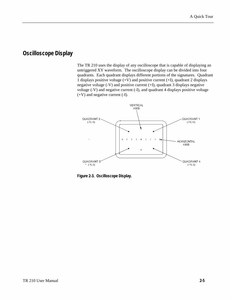
Basic Analog Signatures - Open and Short
In ASA, the two most basic analog signatures are the open and the short. Theopen signature occurs when an output terminal is not connected to anything. Theshort signature occurs when an output terminal is directed connected to thecommon terminal. In the following figures, the upper screen represents theTR 210's oscilloscope X-Y display and the lower screen is a graphical plot of thesine wave test signal at the output terminal showing its current and voltagerelationship. The current and voltage graphical plots are for illustration only andcannot be displayed on the display.
Figure 3-5. "OPEN" Analog Signature on Oscilloscope display (Horizontal Line).
Using Your TR 210
3-6 TR 210 User Manual
Figure 3-6. Test Signal (Open Circuit) with Current and Voltage Waveforms.Minimum Current and Maximum Voltage
Figure 3-7. "SHORT" Analog Signature on the Oscilloscope Display (Vertical Line).
Figure 3-8. Test Signal (Short Circuit) with Current and Voltage Waveforms.Maximum Current and Minimum Voltage

Using Your TR 210
TR210 User Manual 3-7
Four Basic Component Analog Signatures
All analog signatures are a composite of one or more of the four basiccomponent signatures which are: resistance, capacitance, inductance andsemiconductor. Each one of these basic components responds differently toTR 210's test signal, so recognizing these four basic unique signatures on theoscilloscope display are one of the keys to successful ASA troubleshooting.When components are connected together to form a circuit, the signature at eachcircuit node is a composite of the basic component signatures in that circuit. Forexample, a circuit with both resistance and capacitance will have a signature thatcombines the analog signatures of a resistor and capacitor. The signature of aresistor is always indicated by a straight line at an angle from 0 to 90 degrees.The signature of a capacitor is always in the form of a circle or ellipse shape.The signature of an inductor is also a circle or ellipsoid shape, that may alsohave internal resistance. Finally, the semiconductor diode signature is alwaysmade up of two or more linear line segments that most of the time form anapproximate right angle.
RESISTOR CAPACITOR INDUCTOR SEMICONDUCTOR
Figure 3-9. Analog Signatures of 4 Basic Components.

Using Your TR 210
3-8 TR 210 User Manual
Notes:

TR†210 User Manual 4-1
Testing Passive Components
Resistors
Exploring how the TR†210 ranges interact with different resistance values is agood introduction on how basic ASA troubleshooting is applied. This sectionwill briefly familiarize you with TR†210 basic operation and teach you howresistor signatures relate to both test range and the resistance of the circuit undertest. After completing this section, you will know how to:
Apply test probes across a resistor
Identify a pure resistive signature
Analyze and predict resistive signatures
As you go through the following section, make a mental note on the relationshipbetween the TR†210's test range parameters: voltage, resistance and frequency.
Turn power on to your TR†210. Put the red test lead in the A jack, and the blacktest lead in the Common jack.
Figure 4-1. TR 210 with Test Probe Leads.
To display the analog signature of a resistor:
1. Press the LOW2 range button.
2. The LED will be on indicating that LOW2 range is active.

Testing Passive Components
4-2 TR†210 User Manual
3. Place or clip a test lead on the opposite ends of a resistor and observe thesignature on the Oscilloscope CRT display.
Figure 4-2. TR 210 Connected to a Resistor.

Testing Passive Components
TR210 User Manual 4-3
Below are four analog signatures of different resistors, 150, 1.5 k, 15 k and 150 kohms in the upper four ranges. Note how the slope or angle of each analogsignature changes with each resistor's value.
150 Ω 1.5 kΩ 15 kΩ 150 kΩHIGH Range
150 Ω 1.5 kΩ 15 kΩ 150 kΩMED2 Range
150 Ω 1.5 kΩ 15 kΩ 150 kΩMED1 Range
150 Ω 1.5 kΩ 15 kΩ 150 kΩLOW2 Range
Figure 4-3. Signatures of Resistors in Different Ranges.

Testing Passive Components
4-4 TR†210 User Manual
Shorts and Opens, Resistor Faults
Two of the most common faults that occur in electronic components and circuitsare shorts and opens. A short circuit is typically a 0 Ω to 10 Ω low resistive pathbetween two points in a component or circuit that normally would have a higherresistance between them. An open circuit is a break between two points in acomponent or circuit that prevents current from flowing.
Short Open
Figure 4-4. Short and Open Signature.
Review
The signature of a purely resistive circuit is a straight line because therelationship between voltage and current in a purely resistive circuit is linear.
This straight line signature can vary fromñcompletely horizontal (an open)ñcompletely vertical ( a short)
As resistance increasesñcurrent decreasesñthe signature becomes more horizontal
As the range increasesñthe volts per division of the horizontal axis increasesñthe internal resistance increasesñthe signature becomes more vertical

Testing Passive Components
TR210 User Manual 4-5
Troubleshooting Applications
The TR†210 is a fast and efficient continuity tester, providing real timeinformation.
The TR†210 will quickly locate resistor defects, shorts, opens anddegradation that other testers cannot find.
A majority of component failures are resistive in nature. This is important toremember; a component fault may only appear in one range because of theresistive nature of the fault.
The TR†210ís ability to determine the approximate fault resistance valuegreatly enhances the troubleshooting capability if the correct value is known.
The Oscilloscopeís CRT is a real time display and using the TR†210 fortesting noisy or dirty potentiometer (variable resistors) is an excellentapplication. Connect TR†210's test terminals to one fixed pot lead and theother to the pot's wiper lead. Simply monitor the wiper signature whilerotating the pot back and forth. A flawed pot would have the telltaleintermittent angular signature.
Figure 4-5. Using TR 210 to Test a Potentiometer.

Testing Passive Components
4-6 TR†210 User Manual
The TR†210 can be used to adjust a potentiometer in circuit to an approximateoperational setting. This application requires a known good board. Adjust eachpotentiometer on the board under repair to match the settings on a known goodoperational board. In most cases, the board under repair can now be powered upto an operational state where it can be adjusted to true specifications.
Figure 4-6. Using TR 210 to Compare Two Potentiometers.
Capacitors
With a capacitor connected to the TR†210, the test signal across it respondsquite differently than a resistor. The typical analog signature of a capacitor is anelliptical circular pattern and this is due to the fact that relationship between thetest signal's current and voltage are non linear. The current's waveform is 90degrees out of phase with respect to the voltage. The diagram below illustratesthis basic principle for capacitors.
Figure 4-7. Capacitor Circuit with Test Signal's Current and Voltage Waveforms.

Testing Passive Components
TR210 User Manual 4-7
As the test signal's voltage crosses zero volts and becomes more positive, thecurrent flowing in the circuit is at its maximum and becoming smaller. By thetime the voltage has reached its maximum value, the current in the circuit hasceased flowing. As the voltage begins decreasing toward zero, the currentbegins increasing toward maximum. When the voltage reaches zero, the currentis at its maximum value. Similarly, this same pattern follows as the voltage goesnegative.
Because the current is at its maximum value when the voltage is at zero, thecurrent leads the voltage. This is called phase shift and in a purely capacitivecircuit, this phase shift equals 90°. This analog signature appears as a circular orelliptical waveform.
Capacitor Analog Signatures
The goal of this part is to explore some capacitive signatures and to help youunderstand how capacitor signatures are related to:
The capacitance (µf) of the circuit under test
The frequency (Fs) of the test signal
The current range of the TR†210.
Turn power on to your TR†210. Plug the red test microprobe in the A jack, andthe black test clip lead in the Common jack.
CAUTION. The device to be tested must have all power turned off, and have allhigh voltage capacitors discharged before connecting the TR†210 to the device.
Do the following to display the analog signature of a capacitor:
1. Press the LOW2 range button.
2. The buttonís LED will be on indicating that the LOW2 range is active.
3. Place or clip a test lead on the opposite ends of a resistor and observe thesignature on the Oscilloscopeís display.

Testing Passive Components
4-8 TR†210 User Manual
Figure 4-8. TR 210 with Test Probes Connected to a Capacitor.
The Signatures of Different Capacitors in LOW2 Range
The figure below shows analog signatures for four different value capacitors,1000 µf, 100 µf, 10 µf and 1µf. The TR†210 LOW2 range is selected.
1000 µF 100 µF 10 µF 1 µF
Figure 4-9. Signatures Of 4 Capacitors In the LOW2 Range.
Note that as the capacitance values decrease, each signature changes from avertical elliptical pattern to a horizontal elliptical pattern. In ASA, a large valuecapacitor has a signature that looks similar to a short circuit. And likewise, asmall value capacitor has a signature that's similar to an open circuit.

Testing Passive Components
TR210 User Manual 4-9
Understanding Capacitor Analog Signatures
Figure 4-10. TR 210 Core Circuit Block Diagram With A Capacitor.
The Oscilloscopes CRT displays as a response to the test signal, an analogsignature that represents the relationship between voltage, current and resistanceof a component. For circuits that contain capacitors, the effective resistance iscalled capacitive reactance, XC. The mathematical formula is:
Xc = 1
2π fC
XC is inversely related to both capacitance and frequency. So to review andsummarize capacitive analog signatures up to this point:
Changing capacitance: As the capacitance of a circuit increases, thecapacitive reactance XC decreases. This means that when capacitanceincreases, the amount of current in the component or circuit will increase.On the TR†210, the elliptical signature will become increasingly verticalthat implies more current flow.
Changing frequency FS: As the frequency of the test signal increases, thecapacitive reactance XC will decrease and the amount of current in the circuitwill increase. On the TR†210, the elliptical signature will becomeincreasingly vertical that implies more current flow.
Changing the range from LOW1 to HIGH the following occurs:XC of the capacitor is not affectedVS increases so current decreases proportionatelyThe elliptical signature becomes increasingly vertical

Testing Passive Components
4-10 TR†210 User Manual
Capacitor Failures - Leakage
One common physical failure in capacitors is dielectric leakage. The dielectricor insulator in a capacitor normally acts as a non conductor between thecapacitor's two plates. A flawed capacitor develops a conductive or leakage pathbetween its two plates. This can be thought of as a resistance in parallel with thecapacitance when observing its analog signature. The following examples showwhat some capacitor leakage problems may look like on the TR†210 display.
Normal Capacitor Leaky Capacitor
Figure 4-11. Signatures of a 100 µF Capacitor with Dielectric Leakage. LOW2Range, FS = 60 Hz
This example only simulates the leakage flaw by adding a 100 Ω resistor inparallel to a 100 µF capacitor. It shows the signature change from a normalcircular ellipse pattern to a sloped and depressed vertical pattern. The signatureof a real capacitive leakage would be quite similar to this example.
Another example of capacitive leakage is shown for a 10 µF capacitor.
Normal Capacitor Leaky Capacitor
Figure 4-12. Signatures of a 10 µF Capacitor with Dielectric Leakage. LOW2Range, FS = 60 Hz
Again, this example only simulates the leakage flaw by adding a 68 Ω resistor inparallel to a 10 µF capacitor. It shows the signature change from a normalcircular ellipse pattern to a sloped and depressed vertical pattern. The signatureof a real capacitive leakage would be quite similar to this example.
Testing Passive Components
TR210 User Manual 4-11
As you can see from the two previous examples, adding resistance in parallel toa capacitor distorts the normal signature with a diagonal bend to it. This is ourfirst look at a composite signature, the kind of signature the TR†210 displayswhen there are several components connected together in a circuit.
Review
Capacitors have circular or elliptical signatures due to the current andvoltage phase shift.
As the test signal's frequency increases, the capacitor's signature becomesmore vertical due to decreasing XC of the component.
Capacitors with leakage flaws have their ellipses tilted diagonally due to aninternal resistance in parallel with the capacitance.
Applications
The TR†210 can locate defective capacitors in or out of circuit. The rangescover 10 pF to 20,000 µF.
When analyzing a capacitor's signature, adjust the TR†210's ranges andfrequencies for the most pronounced ellipse.
The test signal frequency FS can be changed to enhance a compositesignature by emphasizing or de-emphasizing the capacitance.
Besides resistance, faulty capacitor signatures often exhibit otherirregularities such as non-symmetry, broken or distorted ellipse and saw-toothed shapes that can be seen in on the CRT display.
Inductors
Inductors, like capacitors, have elliptical analog signatures. Also like capacitors,an inductor's reactance (resistance to an AC test signal) is dependent on the testsignal's frequency. Because of the way they are constructed using wire whichsome amount of resistance in it, it is hard to find a pure inductance. Aninductor's analog signature will usually be an elliptical pattern with a some slopeor tilt to it due to the resistance of the coil wire.

Testing Passive Components
4-12 TR†210 User Manual
Inductor Analog Signatures
The goal of this part is to explore some inductive signatures and to help youunderstand how inductor signatures are related to:
The inductance (L in µH) of the circuit under test
The frequency (FS in Hz) of the test signal
The active range of the TR†210
Turn power on to your TR†210. Plug the red test microprobe in the A jack, andthe black test clip lead in the Common jack.
Do the following to display the analog signature of an inductor:
1. Press the LOW2 range button.
2. The LED will be on to indicate that the LOW2 range is activae.
3. Place or clip each test lead on the opposite ends of an inductor and observethe signature on the Oscilloscope CRT display.
Figure 4-13. TR 210 with Probes to an Inductor.

Testing Passive Components
TR210 User Manual 4-13
The Signatures of Different Inductors in LOW2 Range
The figure below shows analog signatures for four different value inductors,12,000 µH, 1200 µH, 120 µH and 12 µH in LOW2 range.
12000 µH 1200 µH 120 µH 12 µH
Figure 4-14. Signatures of 4 Inductors in LOW2 Range. 2000 Hz
Note that as the inductance values decrease, each signature changes from ahorizontal elliptical pattern to a vertical elliptical pattern. In ASA, a large valueinductor has a signature that looks similar to an open circuit. And likewise, asmall value inductor has a signature that's similar to a short circuit.
Affect of Frequency FS on Inductor Signatures
FS = 50/60 Hz FS = 200 Hz FS = 2000 Hz
Figure 4-15. Affect of Varying FS on Inductor Signatures in LOW2
Note that the signature changes from a vertical position to a horizontal positionas the frequency increases. This means the resistance of an inductor increases asfrequency increases.

Testing Passive Components
4-14 TR†210 User Manual
Understanding Inductive Signatures
Figure 4-16. TR 210 Core Circuit Block Diagram with an Inductor.
The TR†210's block diagram shows an inductor between the test terminals. Thecurrent is represented by the vertical axis and is derived as a series current thatflows through TR†210ís internal resistance, RS. The voltage is represented bythe horizontal axis and is derived as a voltage across the inductor.
The formula for the reactance XL of an inductor is:
XL = 2πfL
As the test signal frequency increases, the inductive reactance XL becomeslarger. As a result, the inductorís analog signature will change from a rounderelliptical to a flatter resistive type pattern. The size and shape of the ellipsedepend on the inductor value, test signal frequency, and the selected rangesinternal resistance RS.
Since inductors in reality are not pure inductors, the elliptical signatures theyform on the oscilloscopes display are sometimes distorted. Inductors constructedwith a ferrite core makes the inductive characteristics different from thoseconstructed without. The TR†210 responds with a unique analog signature foreach inductor type.
Review
Inductors display elliptical signatures similar to capacitors. Since theinductor also exhibits resistance, due to its construction, the ellipse may betilted.
As the TR†210 test signalís frequency is increased, the ellipse signaturebecomes flatter. This response is opposite to that of a capacitor.

Testing Passive Components
TR210 User Manual 4-15
As the TR†210 range increases, an inductor's signature becomes morevertical (like the capacitor signature).
When an inductor has a ferrite core, its signature distorts from a non ferriteinductorís ellipse.
Applications
The TR†210 is excellent for troubleshooting inductors. It can reveal shortedor open windings in large variety of inductive components.
Components that are inductors or have inductive characteristics can be foundin many real world applications. For example, some of these are powertransformers, relays, solenoids, flybacks, speakers, magnetic sensors,stepping motors and motor windings.
The best technique for testing inductors is the comparison of a known goodcomponent's signature to a suspect component. For example, a motorarmature has typically numerous windings so every winding should have asimilar analog signature. This fact is true whether it's from an elevator or atape deck. The armature of a DC motor can be tested by simply connectingto the motor brush leads and then adjusting the test range for the mostpronounced or descriptive signature. Slowly turn the armature. Observe theTR†210ís CRT display. This test will check continuity, the inductance, andthe condition of each brush contact without disassembling the motor.
A computer switching power supply contains inductors. For example, acomputer is reported ìdead." To make a quick diagnosis of the possibleproblem first make sure the computer is disconnected from AC power. Thenconnect the red and black test probes across the prongs on the AC line cordgoing to the computer. Turn the computer power switch to the On position.If there is a response on the ProTrack display, adjust the test range for themost pronounced inductive signature. Flick the power switch off and on andwatch for noisy switch contacts. If there is no response, start by checkingeach component up to the primary winding of the transformer. With thistechnique, we have just verified the AC cord, the AC noise filter, the fuse,the power switch and the primary winding of the transformer, withoutremoving the cover of the computer.
Another simple test for a speaker or microphone is to apply the TR†210signal in LOW2 range to the device input leads and listen for the 60 Hz toneor audible hum.
To test solenoids, connect the test probes to the coil leads and manuallymove the plunger or activator in and out while observing if its signaturechanges.

Testing Passive Components
4-16 TR†210 User Manual
Electromechanical Switching Components
Switches are electrical devices that either stop or allow current to flow in acircuit. They are either in an on or off state. Switching devices come in all typesand sizes. There are simple mechanical switches, relays, optical switches, andmany kinds of semiconductor switches. They are different because each uses adifferent kind of stimulus to turn them on or off. Because there are so manykinds of switching devices, there is no single testing procedure that will testthem all completely. With the TR†210, the test signal can be setup so that theswitch's analog signature will verify its switching function. The goal of thissection is to develop a test strategy using ASA to test the switching function.This is not a complete test, but it will be enough to determine whether or not thedevice is functioning as a switch.
Manually Operated Mechanical Switches
A mechanical switch has two states: it is either open or closed. When open, nocurrent can flow; when closed, it acts as a short and allows current to flow. TheTR†210 can test the switching function of mechanically activated switcheseasily. Unlike the DVM that samples and gives a continuity measurement, theTR†210 displays real time activity so if a switch has noisy or intermittentoperation, its analog signature on TR†210's display will reflect these conditions.
Turn power on to your TR†210. Plug the red test microprobe in the A jack, andthe black test clip lead in the Common jack.
Do the following to display the analog signature of a mechanical switch:
1. Press the LOW2 range button.
2. The LED will be on indicating that the LOW2 range is activated.
3. Place or clip each test lead to the switch leads and observe its signature onthe CRT display.
4. Turn the switch to its on or off position.

Testing Passive Components
TR210 User Manual 4-17
Figure 4-17. TR 210 with Probes to an Elastomeric Switch - SPST Type.
MED2 MED1 LOW2
Figure 4-18. Signatures of a Keyboard Pushbutton Conductive Elastomer Switch. SPST Type, "ON" position,
Note that as the ranges change from MED2 to MED1 to LOW2, the signaturetilts away from the vertical. This characteristic is similar to other componentswith internal resistance.
Testing Passive Components
4-18 TR†210 User Manual
Review
The elastomeric switch has significant internal resistance.
As the test signal's voltage decreases with each range change, the volts perdivision of the horizontal axis also decreases so that its analog signaturebecomes more pronounced. This is caused by the small voltage drop acrossthe switch's internal resistance.
Electromechanical Relays
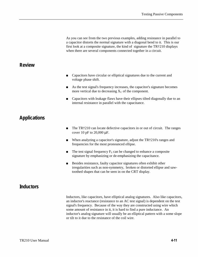
A relay is a switch that's activated by an electrical control input. The relayconsists of switch contacts, magnets and an electromagnetic coil. The TR†210can test the coil part of the relay by looking at its inductive analog signature.You can also connect the TR†210ís pulse generator to the magnetic coil of a 5Vrelay, while at the same time connecting Trackerís test signal to the relaycontacts, to test the relayís switching action directly.
Relay Coil Test
Do the following:
1. Press the LOW2 button .
2. Press the 2000 Hz button.
3. Connect the black test lead from TR†210ís COMMON terminal to one sidethe relay coil (normally, the minus lead).
4. Connect the red test lead from TR†210ís TEST terminal to the other side ofthe relay coil (normally, the plus lead).
Testing Passive Components
TR210 User Manual 4-19
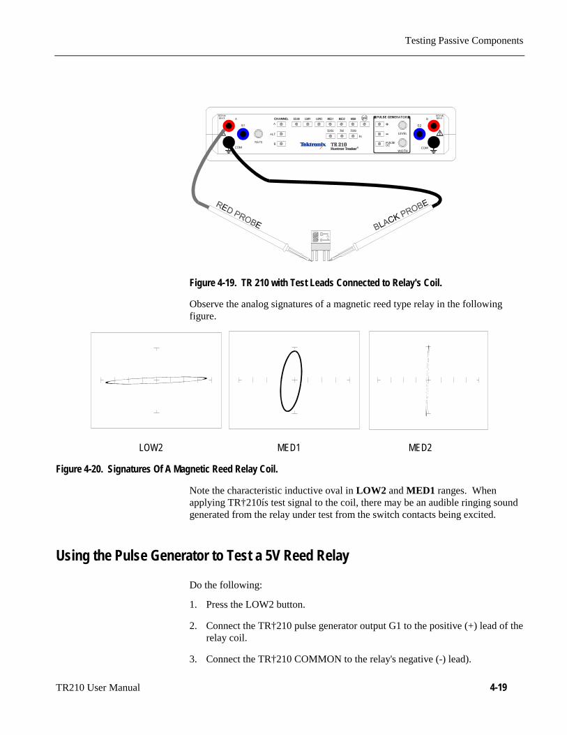
Figure 4-19. TR 210 with Test Leads Connected to Relay's Coil.
Observe the analog signatures of a magnetic reed type relay in the followingfigure.
LOW2 MED1 MED2
Figure 4-20. Signatures Of A Magnetic Reed Relay Coil.
Note the characteristic inductive oval in LOW2 and MED1 ranges. Whenapplying TR†210ís test signal to the coil, there may be an audible ringing soundgenerated from the relay under test from the switch contacts being excited.
Using the Pulse Generator to Test a 5V Reed Relay
Do the following:
1. Press the LOW2 button.
2. Connect the TR†210 pulse generator output G1 to the positive (+) lead of therelay coil.
3. Connect the TR†210 COMMON to the relay's negative (-) lead).

Testing Passive Components
4-20 TR†210 User Manual
4. Connect the black test lead from TR†210ís COMMON terminal to one sideof the relay switch contact.
5. Connect the red test lead from TR†210ís TEST terminal to the other side ofthe relay switch contact.
6. Press Pulse/DC button on the TR†210.
7. Press the + button to activate the positive DC output (+ blue LED should beon).
8. Rotate the Level knob slowly and watch the relay's signature for a shortcircuit. At this point, turn the knob back and forth and watch the relayrelayís signature change between an open and a short.
If the relay does not activate and you know that it is known good, then connectboth pulse generator outputs G1 and G2 in parallel to the relay coil terminal formore output drive current. This will effectively double the drive currentavailable to the device.
Review
The TR†210 can test switches in real time. This makes an excellent test formicroswitches, power switches, control switches, pressure and heat sensorswitches.
As the mechanical switch closes, watch for erratic or discontinous signature.Switch bounce will display as multiple closure signatures. Resistivecontacts will display a resistive signature in LOW2 range.

TR 210 User Manual 5-1
Testing Discrete Semiconductors
Diodes
The most basic type of solid state semiconductor component is the diode.Diodes are formed by creating a junction between p-type and n-typesemiconductor material. The pn junction gives diodes and semiconductorcomponents polarity characteristics that allow them to conduct current when anexternal voltage is applied. They conduct current in one direction, but not in theother. Current flows in a diode when the positive terminal (anode) is made morepositive than the negative terminal (cathode). Figure 5-1 shows how the diodesymbol indicates the polarity of the diode.
Figure 5-1. Diode and Schematic Symbol.
Diode Analog Signatures
Diode signatures demonstrate the fundamental operation of a semiconductorjunction. There is a threshold or forward voltage VF (about 0.6V for a silicondiode) at which the diode begins to conduct current. The diode acts as an opencircuit and no current flows as long as the voltage differential between the anodeand cathode is below that threshold. As the anode to cathode voltage becomesmore positive, the diode will begin to conduct current. Once current begins toflow in the diode, very small increases in anode voltage will cause very largeincreases in current. In analog signature analysis, this is called the ìkneeî effectin a which is characteristic of a good semiconductor junction.
Testing Discrete Semiconductors
5-2 TR 210 User Manual
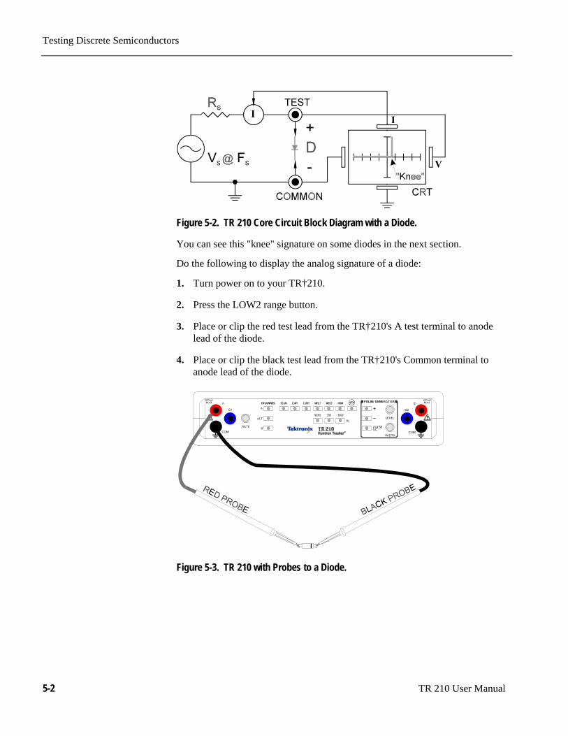
Figure 5-2. TR 210 Core Circuit Block Diagram with a Diode.
You can see this "knee" signature on some diodes in the next section.
Do the following to display the analog signature of a diode:
1. Turn power on to your TR†210.
2. Press the LOW2 range button.
3. Place or clip the red test lead from the TR†210's A test terminal to anodelead of the diode.
4. Place or clip the black test lead from the TR†210's Common terminal toanode lead of the diode.
Figure 5-3. TR 210 with Probes to a Diode.

Testing Discrete Semiconductors
TR 210 User Manual 5-3
LOW2 LOW1
Figure 5-4. Signature of a 1N914 Type Silicon Diode.
Affects of Frequency (FS) on the Diode Signature
With the LOW2 range selected and the test signal frequency of 60 Hz, thesignature of the diode is shown on the left figure below. Changing only the testsignal frequency to 2000 Hz displays the signature on the right. At FS = 2000Hz, the diode's signature has slight circular loop added to it. This loop in thesignature is due to a physical characteristic of diodes called junction capacitance.
60 Hz 2000 Hz
Figure 5-5. Signature of a 1N914 Diode at Different Frequencies.
The Composite Diode Signature
A composite analog signature is a combination of several components connectedtogether in an electronic circuit. Up to this point, we have been showing youwhat the basic component signatures look like out of circuit. In the real world ofelectronics troubleshooting, components are connected together in a circuit andwhen testing with ASA, the signatures are a composite that may appear quitecomplex. However, with knowledge of ASA fundamentals and experience youwill find that even the most complex looking signatures can be analyzed quicklyand efficiently.

Testing Discrete Semiconductors
5-4 TR 210 User Manual
This section will introduce you to some examples of composite diode signatures.
Figure 5-6. Composite Model of a Diode and Capacitor in Parallel.
LOW2 Range, Fs = 60 Hz LOW2 Range, Fs = 2000 Hz
Figure 5-7. Composite Signature - 1N914 Diode and 1 µF Capacitor in Parallel.LOW2 Range.
The signature on the left shows only the diode signature because the test signalfrequency is set below any visible contribution due the capacitive reactance. Thecomposite signature in the center consists of the distinctive loop of the capacitorand the "knee" pattern of the diode. The signature on the right shows only thecapacitor signature because the test signal voltage is below the diode's turn onlevel. When multiple components are connected together, it's important torealize that the TR†210 has the ability to selectively display the signature of asingle component.
Diode Failures
Diodes can fail in a number of ways, and each type of failure will cause thesignature to change. The defective diodes often appear as open and shortsignatures. Two other types of flaws are internal resistance and leakage.

Testing Discrete Semiconductors
TR 210 User Manual 5-5
Internal Resistance Flaw in a Diode
Figure 5-8. Defective Diode Model With A Small Series Resistor.
LOW2 range MED1 range MED2 range
Figure 5-9. Defective Diode Signature with a 50 Ω Series Resistor.
The LOW2 range shows that there is a resistive component to the signature whenthe diode is conducting. This is the result of a defect in the diode's internal PNjunction. The resistance is visible only in LOW2 range because the voltage dropacross it is small. In the other two ranges, the resistance is masked due to theinternal resistances being too large to show such a small voltage drop.

Testing Discrete Semiconductors
5-6 TR 210 User Manual
Internal Leakage Flaw in a Diode
Figure 5-10. Defective Diode Model with an Internal Leakage Resistance.
LOW2 MED1 MED2
Figure 5-11. Signature of a Diode with Internal Leakage Flaw. 1N914 Diode with a 10 kΩ Resistor in Parallel.
Notice that in LOW2 range there does not seem to be any problem, but that inboth medium ranges, you can see the diode conducting when it should be actinglike an open. This is called leakage. The diode acts like a diode when it isforward biased. When reverse biased, the diode acts like a resistor when itshould be acting as an open.
Zener Diodes
Normal switching and signal diodes conduct when forward biased only. Whenreverse biased, they act as opens unless they are operated outside design limits.If this condition occurs then so much voltage is applied that they break down andcan no longer prevent current flow.
A zener diode is a different type of diode and is designed for operation whenreverse biased (diode's cathode connected to positive and anode to negative), butunder carefully controlled conditions. When the zener diode is forward biased(diode's cathode connected to negative and anode connected to positive), they actas regular diodes and begin to conduct at approximately 0.6V.
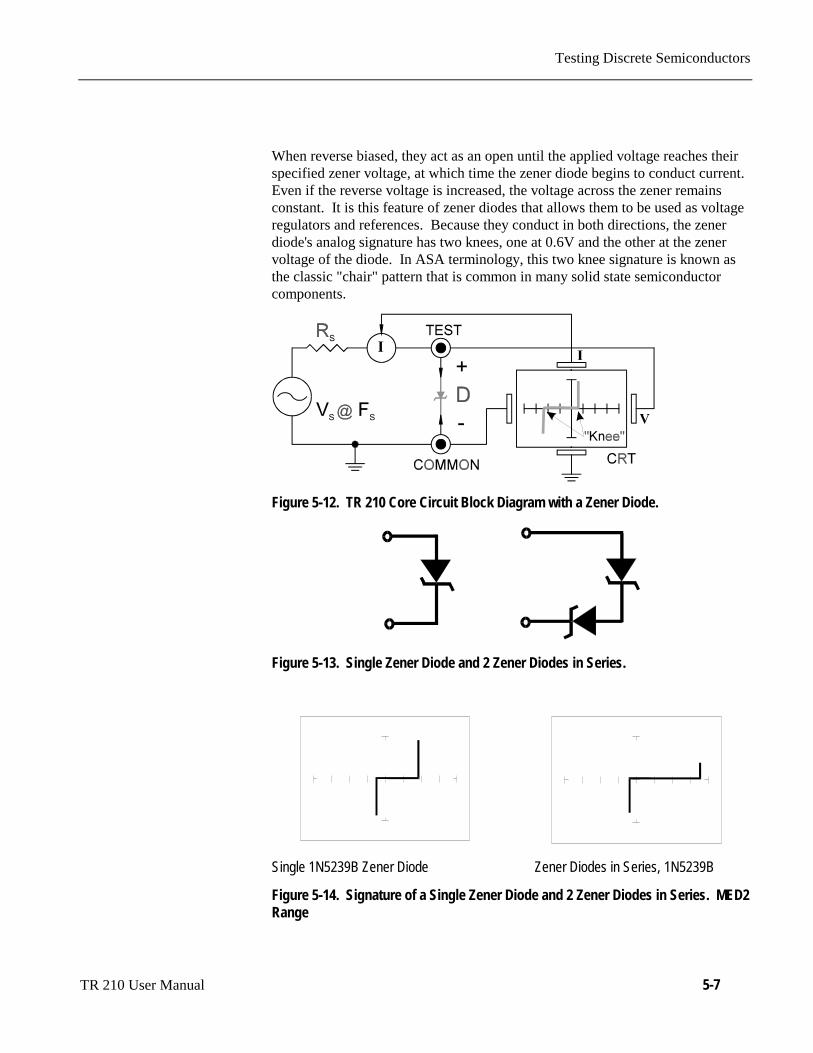
Testing Discrete Semiconductors
TR 210 User Manual 5-7
When reverse biased, they act as an open until the applied voltage reaches theirspecified zener voltage, at which time the zener diode begins to conduct current.Even if the reverse voltage is increased, the voltage across the zener remainsconstant. It is this feature of zener diodes that allows them to be used as voltageregulators and references. Because they conduct in both directions, the zenerdiode's analog signature has two knees, one at 0.6V and the other at the zenervoltage of the diode. In ASA terminology, this two knee signature is known asthe classic "chair" pattern that is common in many solid state semiconductorcomponents.
Figure 5-12. TR 210 Core Circuit Block Diagram with a Zener Diode.
Figure 5-13. Single Zener Diode and 2 Zener Diodes in Series.
Single 1N5239B Zener Diode Zener Diodes in Series, 1N5239B
Figure 5-14. Signature of a Single Zener Diode and 2 Zener Diodes in Series. MED2Range

Testing Discrete Semiconductors
5-8 TR 210 User Manual
Since each horizontal division on the CRT graticule (in MED2 range) isapproximately 5 volts, from the signature on the left you can estimate that this isabout a 9 volt zener diode. The signature at the right is the signature of twozener diodes connected in series. The Zener voltage (VZ) of this circuit is thesum VZ of each of the separate diodes. The signature shows this voltage to beapproximately 18 volts.
Review
Diodes conduct current in one direction (forward biased) and not the other.The diode's analog signature displays this characteristic as the ìkneeî effector pattern.
Diodes have polarity, an anode and a cathode.
Diode defects, other than opens and shorts, are usually resistive.
A diode in series or parallel with a resistor or capacitor will create acomposite signature displaying both characteristics. The TR†210 makes iteasier to separate these characteristics from composite signatures using thetwo parameters, range and FS.
Zener diodes are special diodes that conduct when reverse biased at aspecific voltage.
Applications
Diode damage or degradation can appear as a loss of sharpness or roundingin the ìkneeî.
While faulty diodes display resistive current and voltage legs, they areusually nonlinear or curved.
The polarity of an unmarked diode can be determined by the orientation ofthe display with a known diode.
The TR†210 can be used to identify an unknown zener diode. If the zenerdiode is damaged, locate a good one, possibly on another board or in thesame circuit and use the TR†210 to approximate the voltage.

Testing Discrete Semiconductors
TR 210 User Manual 5-9
Transistors
A bipolar transistor is a three layer device. There are two basic types. A pnptransistor has a layer of n-type silicon material sandwiched between two layersof p-type material. A npn transistor has a layer of p-type silicon materialsandwiched between two layers of n-type material. Figure 5-15 shows therelationship between type of material and circuit symbol for a pnp and a npntransistor.
Figure 5-15. Diagram Of A NPN And PNP Bipolar Transistor.
Bipolar Transistor Signatures
In order to better understand the signatures that transistors create on the TR†210,we can model these devices in terms of equivalent diode circuits. These areshown in figure 5-16. These figures show that the collector-based junctionanalog signature looks similar to a diode signature, and the emitter-base junctionsignature looks similar to a zener diode signature. Because we have already seenthe signatures of these two types of junctions when we tested diodes, they shouldbe familiar to you.

Testing Discrete Semiconductors
5-10 TR 210 User Manual
Figure 5-16. NPN and PNP Bipolar Transistors Equivalent Circuits.
Bipolar Transistor Base-Collector Signatures
CAUTION. A high-frequency bipolar transistor can be degraded by excessivereverse current in its base-emitter junction. The degradation results in a loss ofcurrent gain (hFE). To minimize the possibility of degrading a high-frequencybipolar transistor, use only the MED 2 range when probing its terminals..
Do the following to display the analog signatures of a bipolar transistor:
1. Turn power on to your TR†210.
2. Press the MED2 range button.
3. Place or clip the red test lead from the TR†210's A test terminal to collectorlead of the transistor.
4. Place or clip the black test lead from the TR†210's Common terminal to baselead of the transistor.
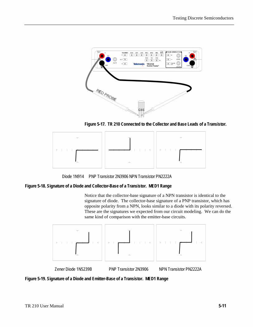
Testing Discrete Semiconductors
TR 210 User Manual 5-11
Figure 5-17. TR 210 Connected to the Collector and Base Leads of a Transistor.
Diode 1N914 PNP Transistor 2N3906 NPN Transistor PN2222A
Figure 5-18. Signature of a Diode and Collector-Base of a Transistor. MED1 Range
Notice that the collector-base signature of a NPN transistor is identical to thesignature of diode. The collector-base signature of a PNP transistor, which hasopposite polarity from a NPN, looks similar to a diode with its polarity reversed.These are the signatures we expected from our circuit modeling. We can do thesame kind of comparison with the emitter-base circuits.
Zener Diode 1N5239B PNP Transistor 2N3906 NPN Transistor PN2222A
Figure 5-19. Signature of a Diode and Emitter-Base of a Transistor. MED1 Range

Testing Discrete Semiconductors
5-12 TR 210 User Manual
We can see that the base-emitter signature of the NPN transistor is nearlyidentical to the signature of the zener diode. The emitter-base signature of a PNPtransistor is also nearly identical but opposite in polarity to the zener diode.
PNP Transistor - 2N3906 NPN Transistor - PN2222A
Figure 5-20. Signature of the Collector-Emitter of a PNP and NPN Transistor. MED1Range, Emitter to Common.
You can see that the collector-emitter signature of a PNP transistor looks like aforward biased diode with the knee at approximately +7 volts. The collector-emitter signature of a NPN transistor looks similar to a reverse biased diode withthe knee at approximately -7 volts.
All bipolar junction transistors have essentially the same looking signatures.
Identifying Unknown Transistors
Sometimes, we need to identify unknown transistors. We may need to replaceone in a circuit for which we do not have a schematic. The TR†210 makes this arelatively simple procedure because each type of junction has a characteristicsignature. This makes it possible to identify each of the terminals and thepolarity of the transistor.
CAUTION. A high-frequency bipolar transistor can be degraded by excessivereverse current in its base-emitter junction. The degradation results in a loss ofcurrent gain (hFE). To minimize the possibility of degrading a high-frequencybipolar transistor, use only the MED 2 range when probing its terminals.
The gate in many power MOSFET transistors is not internally protected and canbe damaged by excessive gate-to-source voltage. To minimize the possibility ofdamage, use only the LOW 2 or MED 1 range when probing power MOSFETtransistors.
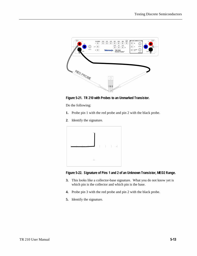
Testing Discrete Semiconductors
TR 210 User Manual 5-13
Figure 5-21. TR 210 with Probes to an Unmarked Transistor.
Do the following:
1. Probe pin 1 with the red probe and pin 2 with the black probe.
2. Identify the signature.
Figure 5-22. Signature of Pins 1 and 2 of an Unknown Transistor, MED2 Range.
3. This looks like a collector-base signature. What you do not know yet iswhich pin is the collector and which pin is the base.
4. Probe pin 3 with the red probe and pin 2 with the black probe.
5. Identify the signature.

Testing Discrete Semiconductors
5-14 TR 210 User Manual
Figure 5-23. Signature of Pins 3 and 2 of an Unknown Transistor, MED2 Range.
6. This looks like a collector-emitter signature.
7. Now that you know that pin 2 of the unknown transistor is the collector.Place the black probe to the base on pin 1 and move the red probe to theemitter on pin 3. A base to emitter signature will be displayed. Thistransistor is a NPN type since the base-emitter signature matches a NPNtransistor.
Figure 5-24. Signature of Pins 1 and 3 of an Unknown Transistor, MED2 Range.
Darlington Bipolar Transistor Signatures
The Darlington transistor is basically two transistors paired together in a specialconfiguration. The emitter of the first transistor is connected to the base of thesecond transistor. The collectors of both transistors are connected together. Thebase of the first transistor serves as the external base lead and the emitter of thesecond transistor serves as the external emitter lead. A block diagram of adarlington transistor and its analog signature are shown in the following figures.

Testing Discrete Semiconductors
TR 210 User Manual 5-15
Figure 5-25. Diagram of a Darlington Transistor.
B-E Junction* C-E Junction** C-B Junction*
Figure 5-26. Signature of a Darlington Transistor, TIP112 NPN Type. MED2 Range, Base to Common*, Emitter toCommon**
NOTE. The B-E junction has a sloped leg bend in its signature caused by internalresistors R1 and R2.
Using the Pulse Generator to Test Transistor Operation
CAUTION. The following technique can inject up to 50 ma into the base of atransistor, which is sufficient current to damage small, high-frequencytransistors. To avoid damage, do not use this technique if the Ic maximumspecification for the transistor is 50 ma or less.
Figure 5-27 shows the test circuit for a NPN transistor using the pulse generatorto drive the base. The constant current signature produced is similar to thatproduced by a transistor curve tracer except that only one curve is shown insteadof a family of curves. This technique can be useful for functionally testing andmatching transistor gain characteristics.

Testing Discrete Semiconductors
5-16 TR 210 User Manual
Figure 5-27. Pulse Generator Test Circuit for a NPN Transistor.
Figure 5-28 shows the test setup for a PNP transistor. As for the NPN transistor,this signature will be the result of the collector-base junction of the transistor.
Figure 5-28. Pulse Generator Test Circuit for a PNP Transistor.
Analyzing the Active Characteristics of a Transistor
Setup:
1. Setup the test circuit shown in figure 5-27 or 5-28 depending on what type ofbipolar transistor you wish to test.
2. Connect the blue grabber test lead from G1 on the TR†210 to the transistor'sbase lead.
3. Press the MED1 range button.
4. Set the frequency to 60 Hz.
Do the following:
1. Press the Pulse/DC button.
2. Press the + button for testing PNP type transistors, or the - button for NPNtesting.
3. Rotate the level knob until the transistor switches on (short circuitsignature).

Testing Discrete Semiconductors
TR 210 User Manual 5-17
Figure 5-29. Testing Transistors with the Pulse Generator - DC Mode, MED1 Range.
4. Press the Pulse/DC button again to select pulse. The Pulse/DC button LEDwill flash on and off.
5. Use the Width knob to adjust the pulse width of the pulse generator output.
Figure 5-30. Testing Transistors with the Pulse Generator - Pulse Mode.
6. Look at the transistor's signature change as the duty cycle changes. Thefigure above shows these signatures as dotted lines. This composite signatureshows multiple operating states as the base stimulus varies. The transistor isactually being switched on and off by the TR†210.
Review
A PNP bipolar transistor consists of a layer of N-type silicon sandwichedbetween two layers of P-type silicon.
A NPN bipolar transistor consists of a layer of P-type silicon sandwichedbetween two layers of N-type silicon.

Testing Discrete Semiconductors
5-18 TR 210 User Manual
To test a transistor, the base-emitter (B-E), collector-base (C-B) andcollector-emitter (C-E) junctions all need to be examined.
The transistor signature resembles the diode signatures previously examined.They have polarity and may exhibit the Zener effect.
Applications
Transistors will display the same type of faulty signature as diodes, with arounded ìkneeî and non-linear or resistive current and voltage legs.
The TR†210 can be used to determine the type of transistor; bipolar,Darlington, FET, etc.
The TR†210 can be used to identify the polarity of a transistor (PNP orNPN).
The TR†210 can be used to determine the base, collector and emitter on anunknown transistor.
The TR†210 can be used to match the gain (beta) of two transistors.
The above techniques of identification are invaluable when repairing foreignelectronics and systems without schematics.
Use the MED2 range when testing high frequency (RF) transistors.
Use the LOW 2 or MED1 range when testing power MOSFET transistors.
Optical Switches
There are two types of optical switches: phototransistors and optocouplers.Phototransistors can be used in two modes depending on the application. It canbe used as either a light activated transistor or as a light activated diode. Ineither mode, light is used to turn it on and allow current to flow.
The optocoupler consists of a light emitting diode and a phototransistor in thesame package. They are electrically isolated. When the diode is turned on by anexternal signal, it radiates light. This light falls on the phototransistor basejunction that results in the device turning on.

Testing Discrete Semiconductors
TR 210 User Manual 5-19
Phototransistors
Figure 5-31. Phototransistor Schematic Diagram.
Do the following to display the analog signature of a phototransistor:
1. Press the MED1 range button.
2. Place or clip the red test lead from the TR†210's A test terminal to collectorlead of the component.
3. Place or clip the black test lead from the TR†210's Common terminal toemitter lead of the component.
Figure 5-32. TR 210 with Test Probes to a Phototransistor.

Testing Discrete Semiconductors
5-20 TR 210 User Manual
No Light With Light
Figure 5-33. Signatures of a NPN Phototransistor - MRD3056 Type. MED1, C-EJunction
The phototransistor's signature is similar to a diode's signature in reversebreakdown mode when not activated by light and as a short signature whenactivated by a bright external light.
Optocoupler Dynamic Testing
The TR†210ís pulse generator can perform a dynamic test of optocouplers.Apply the pulse generator's output to the control input of a switching device andconnect TR†210's test leads across the component's switch terminals. Observethe optocoupler's signature for on and off states.
Figure 5-34. Diagram of an Optocoupler.
Optocoupler Signatures
Do the following to display the analog signature of a optocoupler:
1. Press the MED1 range button.
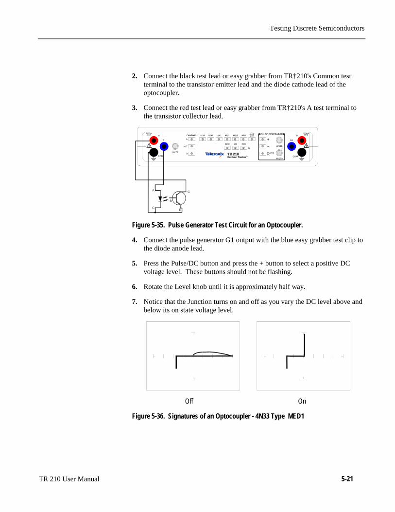
Testing Discrete Semiconductors
TR 210 User Manual 5-21
2. Connect the black test lead or easy grabber from TR†210's Common testterminal to the transistor emitter lead and the diode cathode lead of theoptocoupler.
3. Connect the red test lead or easy grabber from TR†210's A test terminal tothe transistor collector lead.
Figure 5-35. Pulse Generator Test Circuit for an Optocoupler.
4. Connect the pulse generator G1 output with the blue easy grabber test clip tothe diode anode lead.
5. Press the Pulse/DC button and press the + button to select a positive DCvoltage level. These buttons should not be flashing.
6. Rotate the Level knob until it is approximately half way.
7. Notice that the Junction turns on and off as you vary the DC level above andbelow its on state voltage level.
Off On
Figure 5-36. Signatures of an Optocoupler - 4N33 Type MED1
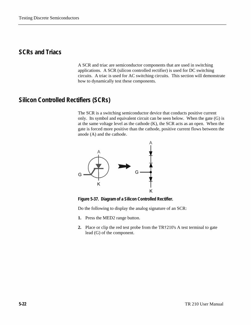
Testing Discrete Semiconductors
5-22 TR 210 User Manual
SCRs and Triacs
A SCR and triac are semiconductor components that are used in switchingapplications. A SCR (silicon controlled rectifier) is used for DC switchingcircuits. A triac is used for AC switching circuits. This section will demonstratehow to dynamically test these components.
Silicon Controlled Rectifiers (SCRs)
The SCR is a switching semiconductor device that conducts positive currentonly. Its symbol and equivalent circuit can be seen below. When the gate (G) isat the same voltage level as the cathode (K), the SCR acts as an open. When thegate is forced more positive than the cathode, positive current flows between theanode (A) and the cathode.
Figure 5-37. Diagram of a Silicon Controlled Rectifier.
Do the following to display the analog signature of an SCR:
1. Press the MED2 range button.
2. Place or clip the red test probe from the TR†210's A test terminal to gatelead (G) of the component.

Testing Discrete Semiconductors
TR 210 User Manual 5-23
Figure 5-38. TR 210 with Test Leads to an SCR.
3. Place or clip the black test probe from the TR†210's Common terminal toanode lead (A) of the component.
4. Observe the gate-anode signature of the SCR.
5. Move the black test probe from the SCR's anode lead to cathode lead (K) ofthe component.
6. Observe the gate-cathode signature of the SCR.
7. Place the red test probe to the SCR's anode lead and the black test probe tothe SCR's cathode lead.
8. Observe the SCR's anode-gate signature.
Gate-Anode Gate-Cathode Anode-Cathode
Figure 5-39. Signatures of an SCR - C106B Type. MED2 Range.

Testing Discrete Semiconductors
5-24 TR 210 User Manual
Active Testing of an SCR
Connect the SCR to the TR†210 as illustrated below:
Figure 5-40. Pulse Generator Test Circuit for a SCR.
Do the following to dynamically test a SCR using the TR†210:
1. Press the MED1 range button.
2. Set the frequency to 50/60 Hz.
3. Press Pulse/DC and press + for selecting DC positive pulse generationvoltage. The Pulse/DC LED should be on and not flashing.
4. Connect the blue easy grabber from TR†210 pulse generator G1 outputterminal to the component's gate lead.
5. Connect the red test probe from TR†210 A test terminal to the SCR's anodelead.
6. Connect the black test probe from TR†210 Common test terminal to theSCR's cathode lead.
7. Turn the Level knob clockwise to increase the voltage level from 0.0VDC.

Testing Discrete Semiconductors
TR 210 User Manual 5-25
Off On
Figure 5-41. Signature of a SCR (C106B Type ) with the Pulse Generator Test.MED1 Range
Observe that as the test voltage increases to about 0.6 volts, the SCR begins toturn on. Watch its signature change from an open signature to a short signature.
Triacs
The TRIAC is a device designed to switch an AC current with either positive ornegative gate control pulses.
Figure 5-42. Diagram and Symbol of a TRIAC.
The next section demonstrates how to dynamically test a triac with the TR†210'spulse generator.

Testing Discrete Semiconductors
5-26 TR 210 User Manual
Active Testing of Triacs
Connect the TR†210 to the TRIAC as shown in figure 5-43.
Figure 5-43. Pulse Generator Test Circuit for a TRIAC.
Do the following to dynamically test a TRIAC using the TR†210:
1. Press the MED2 range button.
2. Set the frequency to 50/60 Hz.
3. Press the Pulse/DC button twice so that the LED flashes.
4. Press the + and - buttons. This invokes both positive and negative goingpulses.
5. Connect the blue easy grabber from TR†210's pulse generator G1 outputterminal to the gate lead on the component.
6. Connect the red test probe from TR†210's A test terminal to the triac's MT2lead.
7. Connect the black test probe from TR†210's Common test terminal to thetriac's MT1 lead.
8. Turn the Level knob clockwise to increase the voltage level.
9. Observe the TRIAC begin to conduct first in a forward direction and then ina reverse direction. You will see that the TRIAC is turned on by pulses ofeither polarity.

Testing Discrete Semiconductors
TR 210 User Manual 5-27
+ Pulse - Pulse +/- Pulse
Figure 5-44. TRIAC Signatures with the Pulse Generator Test. MED2 Range.
Review
Solid state photosensitive switch components are turned on by light.
SCRs and TRIACs are solid state switches that are turned on by a controlinput pin called a gate. SCRs conduct current in one direction whileTRIACs conduct current in both directions.
Applications
The TR†210 can also dynamically test optocouplers and phototransistors.These components are commonly found in isolation and switching circuits.Their operation can slowly deteriorate making them intermittent. This typeof problem is extremely difficult to troubleshoot. With analog signatureanalysis, the TR†210 will detect small amounts of degradation in anoptocoupler's LED and the phototransistor's emitter-collector junction.
The SCR and TRIAC can also be a problem to troubleshoot. They may beused to switch large currents. Quite often these components are susceptibleto degradation and eventual failure. The TR†210 can easily show thesefailures.

Testing Discrete Semiconductors
5-28 TR 210 User Manual
Notes:
TR 210 User Manual 6-1
Testing Integrated Circuits
Digital Integrated Circuits
Digital integrated circuit (IC) chips are made from transistors on a commonsubstrate. Their analog signatures are typically variations of the discrete diodeand transistor signatures. Most logic ICs contain multiple circuits on one chip.These chips can have pins from 14 to over 200, although quite often many pinsshare quite similar signatures. This can make troubleshooting easier by giving usan easy-to-find signature to use as a comparison.
Integrated Circuit Failures
A functioning IC may stop working for a number of reasons. Some of the mostcommon causes of IC failures are:
EOS (Electrical Over Stress) occurs when the ICís maximum electricalspecifications have been exceeded. This condition may result in the ICdeveloping internal shorts and opens.
ESD (Electrostatic Discharge) may cause internal resistance to develop inthe IC junctions. This internal resistance may vary from 5 kΩ to 25 kΩwith a typical value of 20 kΩ. ESD exposure can cause internal flaws suchas resistance, opens and shorts.
Dendrites are a process flaw that results in particles growing betweenconductors on a substrate causing shorts.
Ionic Contamination is contamination introduced at the time ofmanufacturing that develops into leakage between substrate channels. Thiscauses 5 kΩ to 25 kΩ of resistance.
“Purple Plague” is a destructive interaction between gold and aluminummetal layers. Junction connections become very brittle and may causeinternal opens.
Corrosion or Electromigration is another process flaw in which aluminummetalization causes pinholes, corrosion and resistance. This will createopens and resistance.
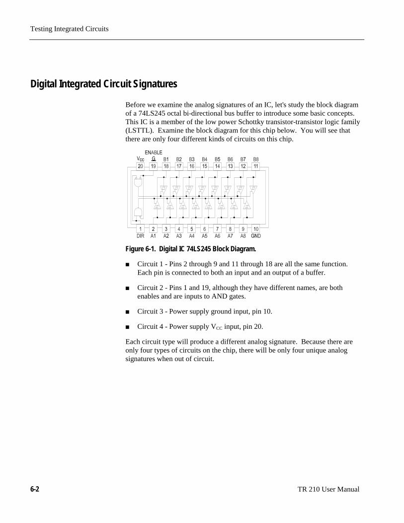
Testing Integrated Circuits
6-2 TR 210 User Manual
Digital Integrated Circuit Signatures
Before we examine the analog signatures of an IC, let's study the block diagramof a 74LS245 octal bi-directional bus buffer to introduce some basic concepts.This IC is a member of the low power Schottky transistor-transistor logic family(LSTTL). Examine the block diagram for this chip below. You will see thatthere are only four different kinds of circuits on this chip.
Figure 6-1. Digital IC 74LS245 Block Diagram.
Circuit 1 - Pins 2 through 9 and 11 through 18 are all the same function.Each pin is connected to both an input and an output of a buffer.
Circuit 2 - Pins 1 and 19, although they have different names, are bothenables and are inputs to AND gates.
Circuit 3 - Power supply ground input, pin 10.
Circuit 4 - Power supply VCC input, pin 20.
Each circuit type will produce a different analog signature. Because there areonly four types of circuits on the chip, there will be only four unique analogsignatures when out of circuit.

Testing Integrated Circuits
TR 210 User Manual 6-3
Signatures of a Digital IC
Do the following to display the analog signatures of a digital IC (out of circuit):
1. Press the MED1 range button.
2. Place or clip the black test lead from the TR†210 Common terminal to theIC's ground pin. For this example, the ground pin of the 74LS245 is pin 10.
3. Use the red test lead from the TR†210 A test terminal. Probe each pin of theIC and view its signature on Oscilloscopes CRT display. For this example,pins 2 to 9 and 11 to 18 are all buffer circuits so they will have identicalsignatures. (Note: This is only for ICs out of circuit.)
4. Use the red test lead from the TR†210 A test terminal. Probe the enableinput pins of the IC and view their signatures on the display. For thisexample, the enable pins of the 74LS245 are pin 1 and 19 and will have thesame signatures. (Note: This is only for ICs out of circuit.)
5. Probe the power supply VCC input pin and view its signature on the CRTdisplay. For this example, the VCC pin of the 74LS245 is pin 20.
Buffer pins - MED1 range Enable pins - MED1 range VCC Power pin - MED1 range
Figure 6-2. Signatures of a Digital IC, 74LS245. Ground Pin to Test Common
Compare these signatures with other signatures of discrete components such astransistors and diodes. Note that there are quite a few similarities here.

Testing Integrated Circuits
6-4 TR 210 User Manual
Signatures for Different Logic Chip Families
There are a wide variety of logic circuit families. Each has its special functions,advantages, and limitations. They range from TTL and its variations (F, LS, S,etc.), emitter-coupled logic (ECL), to the complementary metal oxidesemiconductor (CMOS) and its variations (C, HC, HCT, VC, etc.).
Comparing Two TTL Families
Although the logic function is the same, there are differences in the circuitry ofeach logic family. These differences can be readily seen in their signatures usingthe TR†210.
Figure 6-3. Diagram of 7404 & 74LS04.
We will illustrate these concepts with the following example of two hexinverters, a 7404 and a 74LS04 from different logic families. From the logicdiagram below, you can see that they have the same logic functions and pinorder. The difference is that the LS chip uses Schottky transistors in its internalconstruction for increased performance and reduced power consumption. Notethat there are only four types of circuit connections and therefore only foursignatures on this chip: inverter inputs, inverter outputs, VCC and ground.

Testing Integrated Circuits
TR 210 User Manual 6-5
Pin 1 input - MED1 range Pin 2 output - MED1 range Pin 14 power - MED1 range
Figure 6-4. Signatures of a 7404 Hex Inverter.
Pin 1 input - MED1 range Pin 2 output - MED1 range Pin 14 power - MED1 range
Figure 6-5. Signatures of 74LS04 Hex Inverter.
Note the differences between the two logic families. They have the same logicfunction but different construction, therefore different signatures. To test one ofthese chips without another reference chip available just compare each input'ssignature with the other five inputs. Similarly, compare each output's signaturewith the other five outputs.
CMOS Logic Family
CMOS circuits are constructed differently than TTL circuits. The inputsto CMOS transistors are capacitive due to the use of field-effect transistors(FET) instead of bipolar transistors used in TTL.
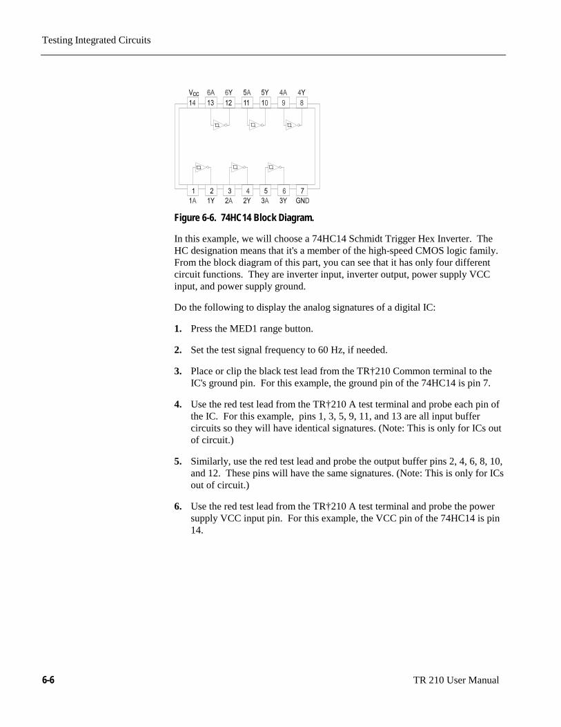
Testing Integrated Circuits
6-6 TR 210 User Manual
Figure 6-6. 74HC14 Block Diagram.
In this example, we will choose a 74HC14 Schmidt Trigger Hex Inverter. TheHC designation means that it's a member of the high-speed CMOS logic family.From the block diagram of this part, you can see that it has only four differentcircuit functions. They are inverter input, inverter output, power supply VCCinput, and power supply ground.
Do the following to display the analog signatures of a digital IC:
1. Press the MED1 range button.
2. Set the test signal frequency to 60 Hz, if needed.
3. Place or clip the black test lead from the TR†210 Common terminal to theIC's ground pin. For this example, the ground pin of the 74HC14 is pin 7.
4. Use the red test lead from the TR†210 A test terminal and probe each pin ofthe IC. For this example, pins 1, 3, 5, 9, 11, and 13 are all input buffercircuits so they will have identical signatures. (Note: This is only for ICs outof circuit.)
5. Similarly, use the red test lead and probe the output buffer pins 2, 4, 6, 8, 10,and 12. These pins will have the same signatures. (Note: This is only for ICsout of circuit.)
6. Use the red test lead from the TR†210 A test terminal and probe the powersupply VCC input pin. For this example, the VCC pin of the 74HC14 is pin14.
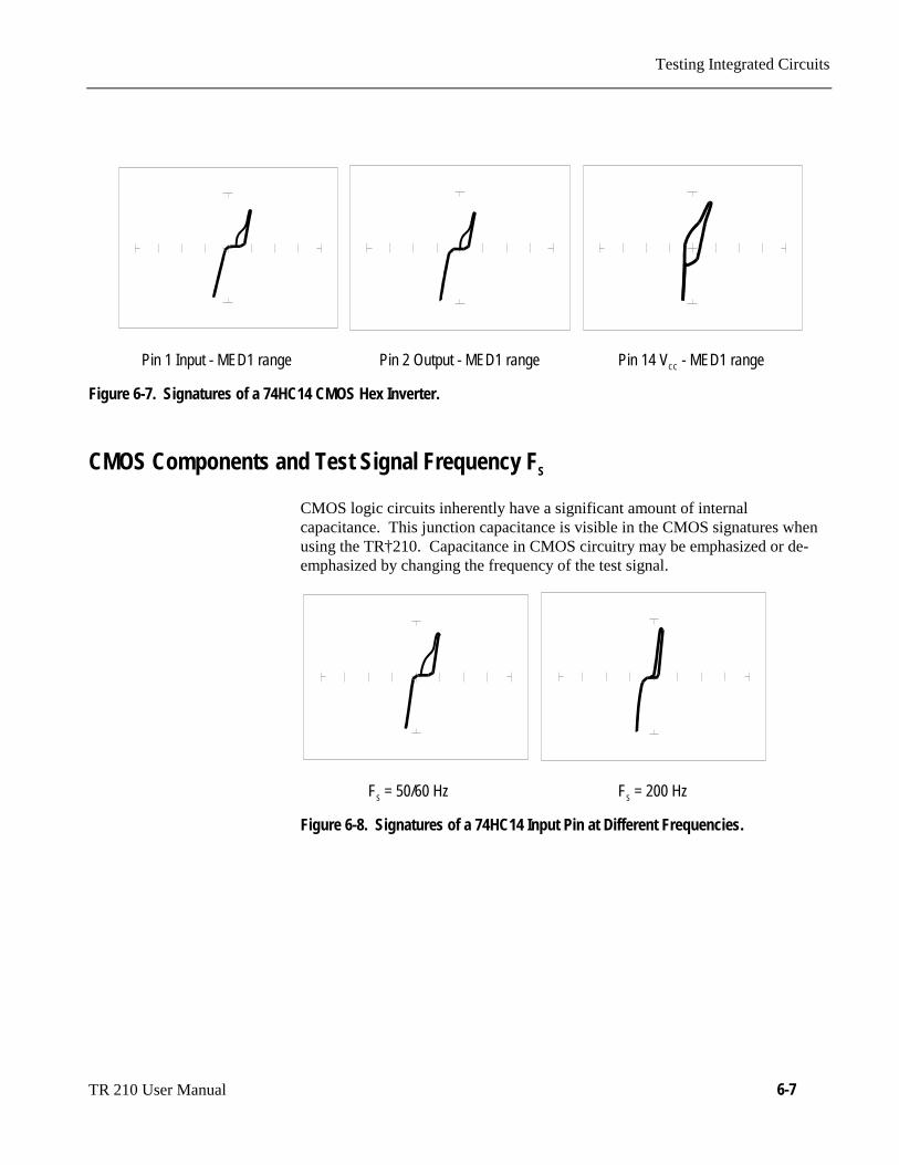
Testing Integrated Circuits
TR 210 User Manual 6-7
Pin 1 Input - MED1 range Pin 2 Output - MED1 range Pin 14 VCC - MED1 range
Figure 6-7. Signatures of a 74HC14 CMOS Hex Inverter.
CMOS Components and Test Signal Frequency FS
CMOS logic circuits inherently have a significant amount of internalcapacitance. This junction capacitance is visible in the CMOS signatures whenusing the TR†210. Capacitance in CMOS circuitry may be emphasized or de-emphasized by changing the frequency of the test signal.
FS = 50/60 Hz FS = 200 Hz
Figure 6-8. Signatures of a 74HC14 Input Pin at Different Frequencies.

Testing Integrated Circuits
6-8 TR 210 User Manual
Troubleshooting Digital Logic ICs
The TR†210 ALT mode makes comparing digital IC signatures quick andsimple. Instead of having to remember the specific signatures of a goodcomponent, all that's needed is to have a reference component or board alongside the one that's suspect. This section gave many examples of signatures fromTTL, Schottky TTL and CMOS logic families. Although from first inspection,these signatures appear to be complex, remember that each of the ICs in theexamples had really only four unique signatures (buffer input, buffer output,power supply VCC and power supply ground). We can use this characteristic todevelop an effective model for troubleshooting digital logic chips.
Figure 6-9. TR 210 with Test Leads Setup for Comparing 2 ICs.

Testing Integrated Circuits
TR 210 User Manual 6-9
Comparison Testing for Digital ICs
Do the following to setup comparison testing and display the analog signaturesof a digital IC:
1. Press the MED1 range button.
2. Set the test signal frequency to 50/60 Hz.
3. Place or connect the black or blue ground clip lead from the TR†210Common terminal to both reference and suspect IC or boards ground pin.
4. Place or clip the black test lead from the TR†210 B test terminal to thesuspect IC's pin. For this example, start with pin 1 of the suspect IC.
5. Place or clip the red test lead from the TR†210 A test terminal to thereference or known good IC's pin. For this example, start with pin 1 of theknown good IC.
6. Push the Channel A button. Observe the signature. This is the signature ofthe pin of the known good component.
7. Push the Channel B button. Observe the signature. This is the signature ofthe pin of the suspect component.
Or press the Alt button to display the A and B channels alternately. Rotatethe Rate knob to change the speed of alternating between the two channels.
8. Visually compare the reference signature (channel A) with the suspectsignature (channel B).
9. Keep the red probe on pin 1, an input pin. Probe all the other input pins ofthe suspect component with the black probe until you have identified all thepins that have signatures that are the same as pin 1.
10. Move the red probe on pin 2, an output pin. Probe all the other output pinsof the suspect component with the black probe until you have identified allthe pins that have signatures that are the same as pin 2.

Testing Integrated Circuits
6-10 TR 210 User Manual
Review
Integrated circuits are complex devices that are built using basic electroniccomponents.
The IC signatures resemble zener diodes.
There are many causes for IC failures and the TR†210 can display its"health" as resistive leakage, an open or a short.
Functionally identical pins on a single IC out-of-circuit will display the samesignature.
The most common point for reference is ground, but VCC or another pointmight give a more informative signature.
Different logic families exhibit different characteristic signatures.
To simplify the large number of signature variations, use the comparison teststrategy with the TR†210. The TR†210 features alternately switchingdisplay of the A and B channels to allow comparison of two individualsignatures
Applications
Testing for faulty ICís is one of the more common uses for the TR†210. Atechnician can compare ICís in or out of circuit.

Testing Integrated Circuits
TR 210 User Manual 6-11
Analog Circuits
Analog components and circuits represent another family of integrated circuitcomponents and include operational amplifiers (op amps), comparators,references, regulators, timers and many other specialized functions. Thesecomponents and circuits present more troubleshooting challenges that are uniqueto this particular family of ICs.
Op Amps
Frequently, each pin of an op amp creates a different signature on the TR†210.This signature is the result of the internal design of the chip and both the internaland external circuit elements connected to it. This type of analog componenttypically has many internal junctions connected to each pin and each pin mayalso be connected to numerous external components.
The following example will demonstrate ASA with a commonly used 741 typeop amp. In this case it is configured as an inverting amplifier circuit as in theschematic below.
Figure 6-10. Op Amp Symbol and Schematic Diagram of an Inverter Circuit.
We will examine the signatures of this analog IC and present sometroubleshooting concepts for this type of component.

Testing Integrated Circuits
6-12 TR 210 User Manual
Op Amp Signatures
Figure 6-11. TR 210 with Test Leads to an Op Amp.
Do the following to display the analog signatures of an op amp:
1. Press the MED1 range button.
2. Set the test signal frequency to 50/60 Hz.
3. Place or clip the black test lead from the TR†210 Common terminal to theIC's ground or a power supply pin. For this example, the negative powersupply pin of the 741 is pin 4 and the positive power supply is pin 8.
4. Use the red test lead from the TR†210 A test terminal and probe each pin ofthe IC.
5. Observe that the signature of each of the op amp's pins are unique.
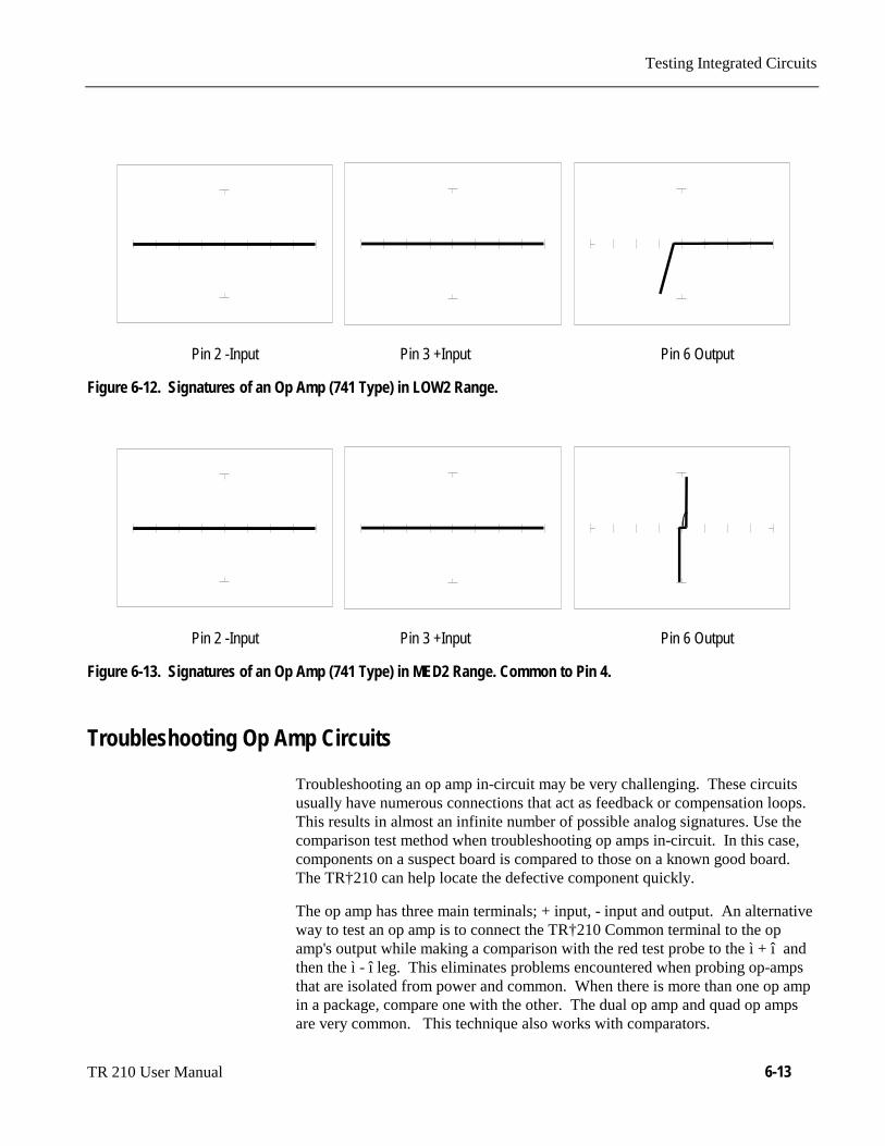
Testing Integrated Circuits
TR 210 User Manual 6-13
Pin 2 -Input Pin 3 +Input Pin 6 Output
Figure 6-12. Signatures of an Op Amp (741 Type) in LOW2 Range.
Pin 2 -Input Pin 3 +Input Pin 6 Output
Figure 6-13. Signatures of an Op Amp (741 Type) in MED2 Range. Common to Pin 4.
Troubleshooting Op Amp Circuits
Troubleshooting an op amp in-circuit may be very challenging. These circuitsusually have numerous connections that act as feedback or compensation loops.This results in almost an infinite number of possible analog signatures. Use thecomparison test method when troubleshooting op amps in-circuit. In this case,components on a suspect board is compared to those on a known good board.The TR†210 can help locate the defective component quickly.
The op amp has three main terminals; + input, - input and output. An alternativeway to test an op amp is to connect the TR†210 Common terminal to the opamp's output while making a comparison with the red test probe to the ì + î andthen the ì - î leg. This eliminates problems encountered when probing op-ampsthat are isolated from power and common. When there is more than one op ampin a package, compare one with the other. The dual op amp and quad op ampsare very common. This technique also works with comparators.
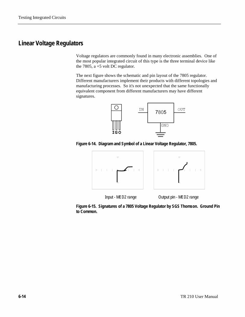
Testing Integrated Circuits
6-14 TR 210 User Manual
Linear Voltage Regulators
Voltage regulators are commonly found in many electronic assemblies. One ofthe most popular integrated circuit of this type is the three terminal device likethe 7805, a +5 volt DC regulator.
The next figure shows the schematic and pin layout of the 7805 regulator.Different manufacturers implement their products with different topologies andmanufacturing processes. So it's not unexpected that the same functionallyequivalent component from different manufacturers may have differentsignatures.
Figure 6-14. Diagram and Symbol of a Linear Voltage Regulator, 7805.
Input - MED2 range Output pin - MED2 range
Figure 6-15. Signatures of a 7805 Voltage Regulator by SGS Thomson. Ground Pinto Common.
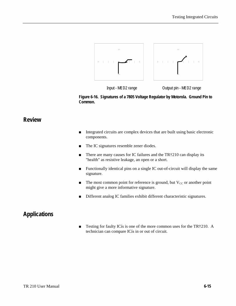
Testing Integrated Circuits
TR 210 User Manual 6-15
Input - MED2 range Output pin - MED2 range
Figure 6-16. Signatures of a 7805 Voltage Regulator by Motorola. Ground Pin toCommon.
Review
Integrated circuits are complex devices that are built using basic electroniccomponents.
The IC signatures resemble zener diodes.
There are many causes for IC failures and the TR†210 can display its"health" as resistive leakage, an open or a short.
Functionally identical pins on a single IC out-of-circuit will display the samesignature.
The most common point for reference is ground, but VCC or another pointmight give a more informative signature.
Different analog IC families exhibit different characteristic signatures.
Applications
Testing for faulty ICís is one of the more common uses for the TR†210. Atechnician can compare ICís in or out of circuit.

Testing Integrated Circuits
6-16 TR 210 User Manual
Low Voltage
There is a new family of logic that offers lower dynamic power consumption,lower operating voltages, higher output drive, faster AC speed, lower noise andbetter dynamic thresholds than HC CMOS. These features make this familyattractive for low power applications such as battery operated portableapplications (that is, laptop computers, pagers, phones, etc.).
In order to achieve this new improved level of performance, the manufacturers ofthis LV (low voltage) family of logic ICs have redesigned the internal structureof the device. Some manufacturers have changed the input structure byeliminating the input protection diode to VCC. Similarly, the design of theoutput structure also has changed by eliminating the output protection diode toVCC and replacing it with a N-Channel pull-up transistor. As a result of thesechanges, the analog signatures of the LV logic family are different from theconventional HC logic family.
The TR†210 has the built-in "SMT" test range group which has been optimizedfor this LV logic. SMT is an abbreviation for surface mount technology andrefers to the physical IC package type in which the LV logic family is commonlyavailable.
Figure 6-17. TR 210 with Test Probes to a 20 Pin Surface Mount IC.
1. Press the LOW1 range button.
2. Set the test signal frequency to 50/60 Hz.
3. Place or clip the black test lead from the TR†210 Common terminal to theIC's ground pin. For this example, the ground pin of the 74LVQ245 is pin10.

Testing Integrated Circuits
TR 210 User Manual 6-17
4. Use the red test lead from the TR†210 A test terminal and probe each pin ofthe IC. For this example, pins 2 to 9 and 11 to 18 are all buffer circuits sothey will have identical signatures. (Note: This is only for ICs out of circuit.)
5. Use the red test lead from the TR†210 A test terminal and probe the enableinput pins. For this example, the enable pins of the 74LVQ245 are pin 1 and19 and will have the same signatures. (Note: This is only for ICs out ofcircuit.)
6. Use the red test lead from the TR†210 A test terminal and probe the powersupply VCC input pin. For this example, the VCC pin of the 74LVQ245 ispin 20.
Buffer pins - LOW1 range Enable pins - LOW1 range VCC Power pin - LOW1 range
Figure 6-18. Signatures of a Low Voltage IC (74LVQ45 Type). Ground Pin to Common.
The LOW1 test range have been developed to enhance the resistive faultsignatures that are commonly found when troubleshooting this logic family. Thetest signal voltage VS is lower than theLOW2 range to ensure that mostdescriptive signature is displayed. A higher VS may result is a signature goingtoward a short with would mask out flaws. The short signature can be attributedby the LV family's lower voltage characteristics.
Compare these signatures with the CMOS logic family and other discretecomponents such as transistors and diodes. Note that these signatures have somecommon similarities with the other components' analog signature we have seenalready.

Testing Integrated Circuits
6-18 TR 210 User Manual
Review
Integrated circuits are complex devices that are built using basic electroniccomponents.
The IC signatures resemble regular and zener diode signatures.
There are many causes for IC failures and the TR†210 can display its"health" as resistive leakage, an open or a short.
Functionally identical pins on a single IC out-of-circuit will display the samesignature.
The most common point for reference is ground, but VCC or another pointmight give a more informative signature.
Applications
Testing for faulty ICís is one of the more common uses for the TR†210. Atechnician can compare ICís in or out of circuit.