Embed Size (px)
Citation preview

USB-TTL Interface Module Reference Manual
Version 1.1

ii
Copyright © 2006, 2007 Elba Corp. All rights Reserved. Publication History
May 2006 – Beta release January 2007 – First public release Disclaimer
Elba Corp. makes no warranty regarding the accuracy of or the fitness for any particular purpose of the information in this document or the techniques described herein. The reader assumes the entire responsibility for the evaluation of and use of the information presented. The Company reserves the right to change the information described herein at any time without notice and does not make any commitment to update the information contained herein. No license to use proprietary information belonging to the Company or other parties is expressed or implied.
Trademarks
ZBasic, ZX-24, ZX-24a, ZX-40, ZX-40a, ZX-44 and ZX-44a are trademarks of Elba Corp. Other brand and product names are trademarks or registered trademarks of their respective owners.
iii
Table of Contents
Introduction................................................................................................................................... 1
Connections and Jumpers ......................................................................................................... 1
J2...............................................................................................................................................2
J3, J4 ........................................................................................................................................ 2
J5...............................................................................................................................................2
J6...............................................................................................................................................2
J7...............................................................................................................................................2
LEDs ......................................................................................................................................... 3
Assembly Tips.........................................................................................................................3
Example of Use Connecting to a ZX microcontroller........................................................3
Drivers........................................................................................................................................... 4
Installing the CDM Driver for the USB-TTL Interface Module..............................................4
Configuring the USB-TTL Interface Module............................................................................ 8
Schematic...................................................................................................................................14

iv
This page is intentionally blank.

1
USB-TTL Interface Module
Introduction The USB-TTL Interface Module (for brevity, Module hereafter) can be used to add USB connectivity to any microcontroller or other device that is capable of standard serial communication. There are several configuration options on the Module that facilitate its use in a variety of situations. The Module can be powered from the USB hub or from an external supply. When powered by the USB hub, the Module can optionally provide power to external circuitry. The Module can be configured for either a 5 volt or a 3.3 volt signal interface and it can provide 3.3 volt power to external circuitry as well, subject to current limits. The pinout of the Module is designed to make it very easy to use with a ZX-24 or other microcontroller that uses the standard Basic Stamp pinout. The transmit data, receive data, DTR and ground connections are in the correct order so that the Module can be directly connected to a compatible microcontroller on a solderless breadboard. The Module is provided completely assembled except for the jumper connections and the I/O signal connections. These are left to the user to install, if desired. Alternately, the Module may be directly wired into another circuit and jumper wires may be soldered in place.
Connections and Jumpers The Module connects to a USB hub via a standard USB cable that has a Type A connector on one end (plugs into the hub) and a Type B connector on the other end (plugs into the J1 jack on the Module). The Module is connected to external circuitry via the J2, J3 and/or J4 terminals on the Module.
2
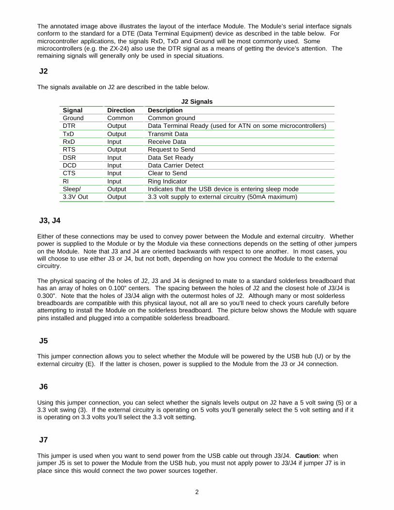
The annotated image above illustrates the layout of the interface Module. The Module’s serial interface signals conform to the standard for a DTE (Data Terminal Equipment) device as described in the table below. For microcontroller applications, the signals RxD, TxD and Ground will be most commonly used. Some microcontrollers (e.g. the ZX-24) also use the DTR signal as a means of getting the device’s attention. The remaining signals will generally only be used in special situations.
J2 The signals available on J2 are described in the table below.
J2 Signals
Signal Direction Description Ground Common Common ground DTR Output Data Terminal Ready (used for ATN on some microcontrollers)
TxD Output Transmit Data RxD Input Receive Data RTS Output Request to Send
DSR Input Data Set Ready DCD Input Data Carrier Detect CTS Input Clear to Send
RI Input Ring Indicator Sleep/ Output Indicates that the USB device is entering sleep mode 3.3V Out Output 3.3 volt supply to external circuitry (50mA maximum)
J3, J4 Either of these connections may be used to convey power between the Module and external circuitry. Whether power is supplied to the Module or by the Module via these connections depends on the setting of other jumpers on the Module. Note that J3 and J4 are oriented backwards with respect to one another. In most cases, you will choose to use either J3 or J4, but not both, depending on how you connect the Module to the external circuitry. The physical spacing of the holes of J2, J3 and J4 is designed to mate to a standard solderless breadboard that has an array of holes on 0.100” centers. The spacing between the holes of J2 and the closest hole of J3/J4 is 0.300”. Note that the holes of J3/J4 align with the outermost holes of J2. Although many or most solderless breadboards are compatible with this physical layout, not all are so you’ll need to check yours carefully before attempting to install the Module on the solderless breadboard. The picture below shows the Module with square pins installed and plugged into a compatible solderless breadboard.
J5 This jumper connection allows you to select whether the Module will be powered by the USB hub (U) or by the external circuitry (E). If the latter is chosen, power is supplied to the Module from the J3 or J4 connection.
J6 Using this jumper connection, you can select whether the signals levels output on J2 have a 5 volt swing (5) or a 3.3 volt swing (3). If the external circuitry is operating on 5 volts you’ll generally select the 5 volt setting and if it is operating on 3.3 volts you’ll select the 3.3 volt setting.
J7 This jumper is used when you want to send power from the USB cable out through J3/J4. Caution: when jumper J5 is set to power the Module from the USB hub, you must not apply power to J3/J4 if jumper J7 is in place since this would connect the two power sources together.
3
LEDs The Module has a bi-color LED that indicates activity. The red LED flashes when the Module receives data and the green LED flashes when the Module transmits data.
Assembly Tips If you plan to solder square pins to the board to connect the converter to a solderless breadboard, the simplest way to do so is to insert the square pins for J2 and J3/J4 into the solderless breadboard and then place the board over the pins and solder them. This ensures that the pins are not misaligned. For the jumper pins that are installed from the top of the board (J5, J6 and J5) the same technique can be used, placing the board down over the pins and soldering them.
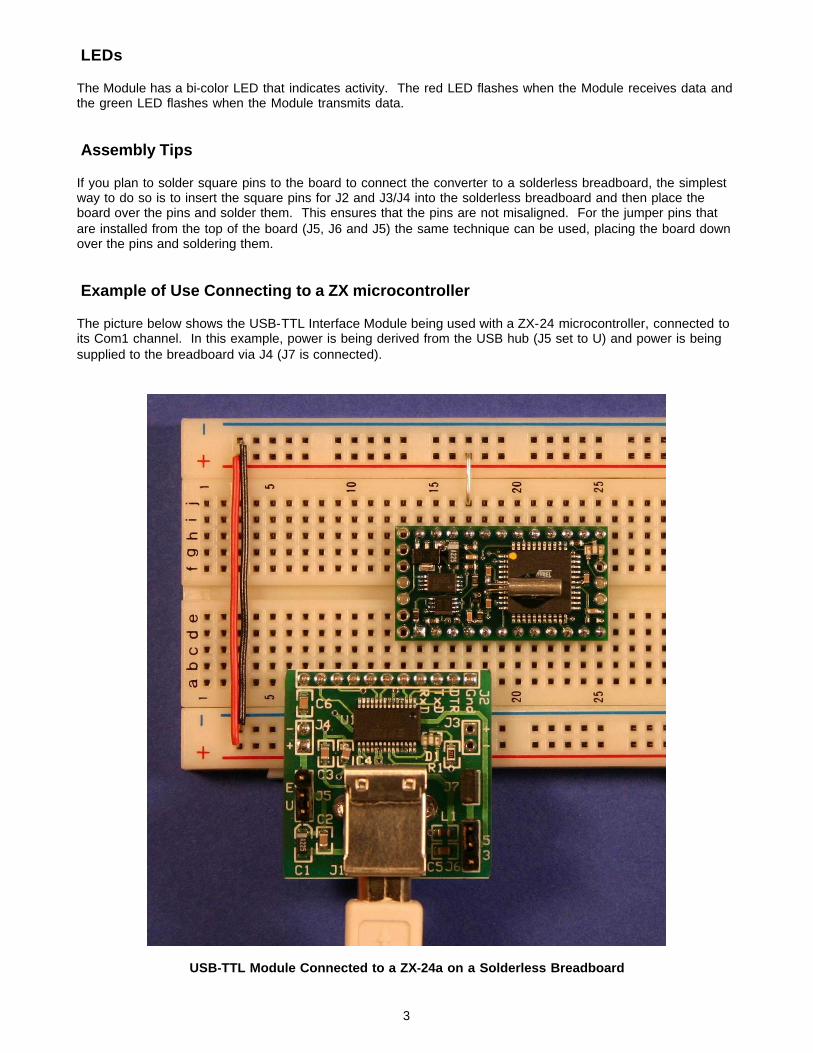
Example of Use Connecting to a ZX microcontroller The picture below shows the USB-TTL Interface Module being used with a ZX-24 microcontroller, connected to its Com1 channel. In this example, power is being derived from the USB hub (J5 set to U) and power is being supplied to the breadboard via J4 (J7 is connected).
USB-TTL Module Connected to a ZX-24a on a Solderless Breadboard

4
Drivers Installation guides for the FTDI FT232R drivers are available for several operating systems at http://www.ftdichip.com/Documents/InstallGuides.htm. Prior to version 2.0, FTDI had two separate device drivers for the FT232R chip. The Virtual Comm Port (VCP) driver provided a serial COM port that is similar to a hardware serial port while the D2XX driver provided a DLL interface. Recently, FTDI introduced a new driver that combines both of these sets of capabilities into a single driver called the Combined Driver Module (CDM). If you already have other FTDI-based USB devices on your system that support the FT232R you shouldn’t need to install new CDM. Note, however, that changing the configuration of the USB interface (which requires the D2XX DLL interface) is simpler with the CDM driver installed. Otherwise, you must first remove the VCP driver, install the D2XX driver, configure the device, remove the D2XX driver and re-install the VCP driver. For this reason, you may wish to install the CDM driver. The FT232R drivers are available directly from FTDI at http://www.ftdichip.com/Drivers/VCP.htm. Note that the CDM driver is not available for all operating systems. Be sure to download the drivers for the FT232R device that match your OS.
Installing the CDM Driver for the USB-TTL Interface Module For driver installation, the interface chip on the Module needs to be powered. The simplest method for powering the chip is to set J5 to the “U” position so that the Module will be powered from the USB hub. Alternately, you may power the chip via J3/J4 with J5 in the “E” position. If you choose to power the Module from the USB hub, no other connections to the Module are necessary at this point. The following procedure describes the steps that are required to install the CDM driver for the Module on a Windows XP computer. The steps for other operating systems are similar, consult the FTDI installation guide for your OS. It is assumed that the CDM driver archive has been downloaded and the files extracted to the directory C:\drivers\FT232R.
1) Connect a USB type A/B cable (not included) from the computer’s USB port (or USB hub) to the J1 connector on the Module. This will cause the OS to recognize the device as an “FT232R USB UART”. If you have previously installed another USB-serial adapter that uses the standard FTDI VCP or CDM driver, the OS will likely associate that driver with the Module. If it does not, proceed with the following steps.
5
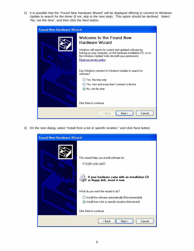
2) It is possible that the “Found New Hardware Wizard” will be displayed offering to connect to Windows Update to search for the driver (if not, skip to the next step). This option should be declined. Select “No, not this time”, and then click the Next button.
3) On the next dialog, select “Install from a list or specific location.” and click Next button.
6
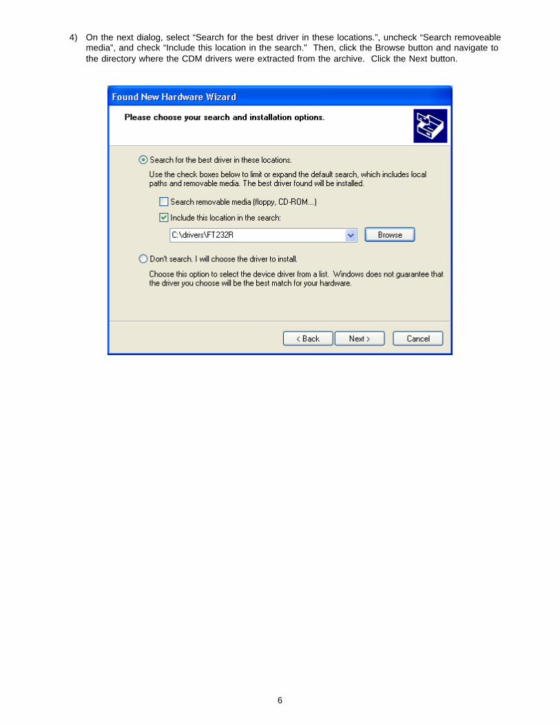
4) On the next dialog, select “Search for the best driver in these locations.”, uncheck “Search removeable media”, and check “Include this location in the search.” Then, click the Browse button and navigate to the directory where the CDM drivers were extracted from the archive. Click the Next button.

7
5) The OS should install the drivers and then present a dialog indicating that the process has completed. Click the Finish button.
6) Next, the preceding sequence may need to be repeated, this time for installing the COM port associated with the Module. When the driver has been properly installed, you should have a new COM port on your computer. You can verify that this is the case by selecting Settings | Control Panel from the Start menu and double-clicking the System tool. Next, click the Hardware tab and then the “Device Manager” button. The new COM port should show up under “Ports (COM & LPT)” as shown in the image below.
8
7) If a new COM port did not appear, check the “Other Devices” section and see if there is a USB device listed there. If so, that indicates that the driver did not get installed correctly. This can usually be rectified simply by reinstalling the driver. You can initiate this process by right-clicking on the USB device listed under “Other Devices” and selecting “Update Driver”. From there, the steps are a repeat of those given above beginning at step 2.
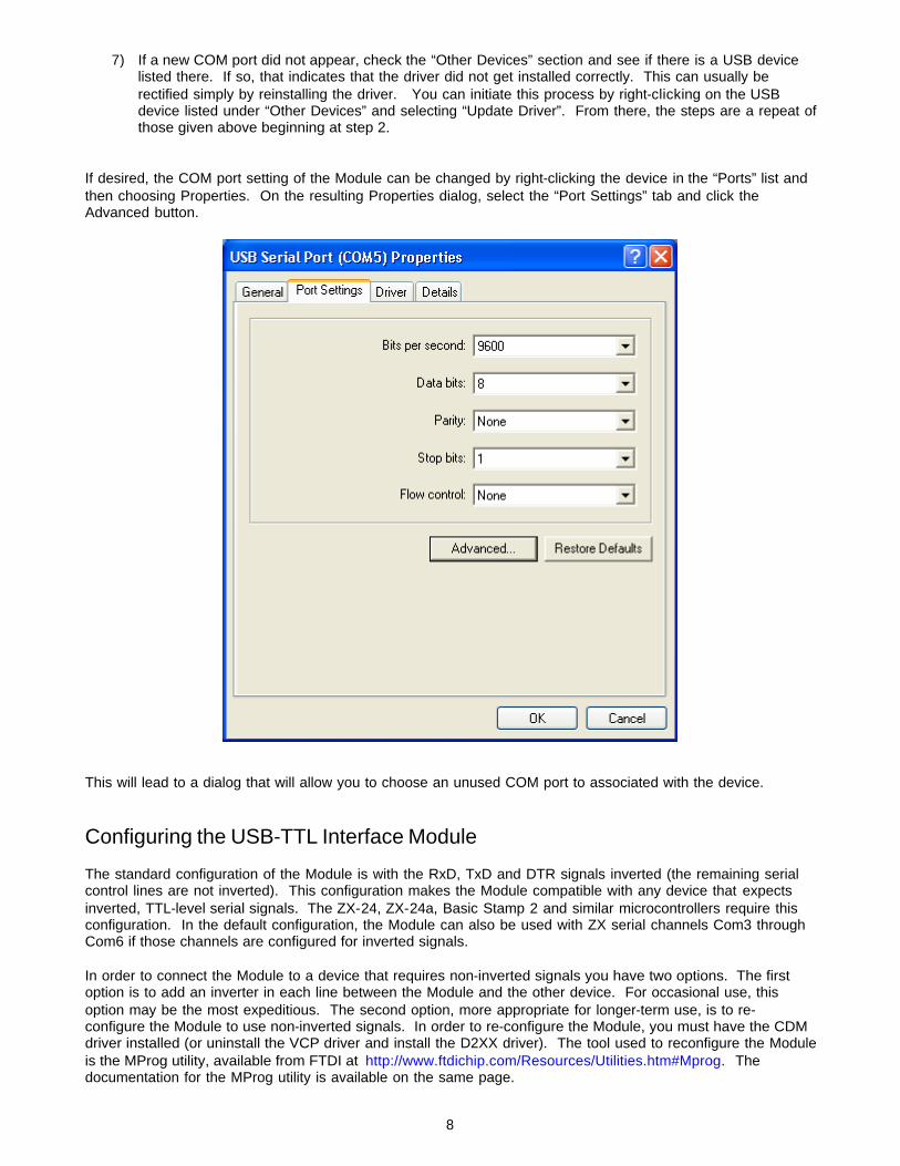
If desired, the COM port setting of the Module can be changed by right-clicking the device in the “Ports” list and then choosing Properties. On the resulting Properties dialog, select the “Port Settings” tab and click the Advanced button.
This will lead to a dialog that will allow you to choose an unused COM port to associated with the device.
Configuring the USB-TTL Interface Module The standard configuration of the Module is with the RxD, TxD and DTR signals inverted (the remaining serial control lines are not inverted). This configuration makes the Module compatible with any device that expects inverted, TTL-level serial signals. The ZX-24, ZX-24a, Basic Stamp 2 and similar microcontrollers require this configuration. In the default configuration, the Module can also be used with ZX serial channels Com3 through Com6 if those channels are configured for inverted signals. In order to connect the Module to a device that requires non-inverted signals you have two options. The first option is to add an inverter in each line between the Module and the other device. For occasional use, this option may be the most expeditious. The second option, more appropriate for longer-term use, is to re-configure the Module to use non-inverted signals. In order to re-configure the Module, you must have the CDM driver installed (or uninstall the VCP driver and install the D2XX driver). The tool used to reconfigure the Module is the MProg utility, available from FTDI at http://www.ftdichip.com/Resources/Utilities.htm#Mprog. The documentation for the MProg utility is available on the same page.
9
The following procedure describes the steps that are required to re-configure the Module on a Windows XP computer. The steps for other operating systems are similar. It is assumed that the MProg utility has already been downloaded to the target computer and installed and that either the CDM or D2XX driver has been properly installed. Note that if the CDM driver is being used, the COM port associated with the device must not be currently in use by any application. If it is in use, error will occur or the device won’t show up in the scan procedure described below.
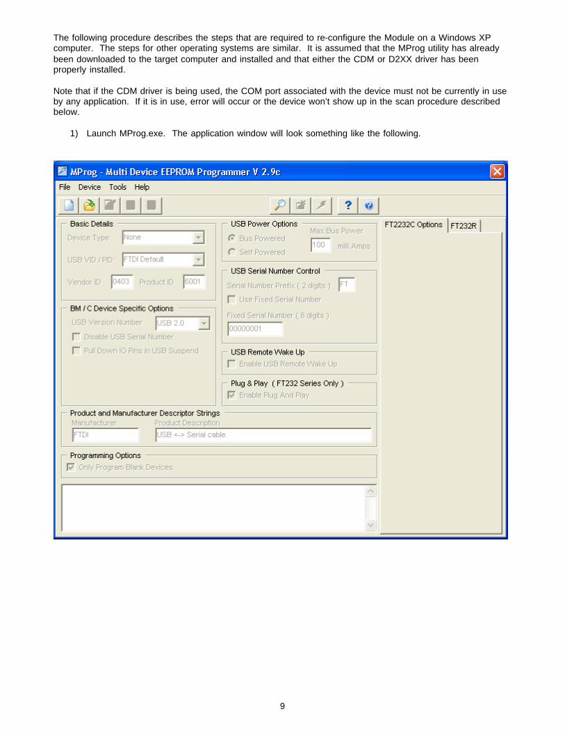
1) Launch MProg.exe. The application window will look something like the following.

10
2) Select “Scan” from the Device menu. If you have your Module powered and connected to the computer, you should see something like the following. Note particularly the text in the box near the bottom. In this instance, the scan has found only 1 device and it is is in the “programmed” state. If you have other FT232-based devices connected to the computer you will likely see evidence of additional devices. In order to avoid changing the programming of the other devices you should temporarily disconnect them from their hubs and perform the scan again.

11
3) Select “Read and Parse” from the Tools menu. The current configuration of the Module will be displayed as depicted below. In this case, the standard Module configuration is shown with inverted TxD, RxD and DTR. Note that the title bar contains the phrase “Edit Mode”. This signifies that you may change the configuration parameters that are displayed. If the title bar does not indicate edit mode, you can change to edit mode using the “Edit” entry of the “File” menu. If that entry is greyed out, you may have to save the current configuration data first using the “Save As…” entry on the “File” menu.
12
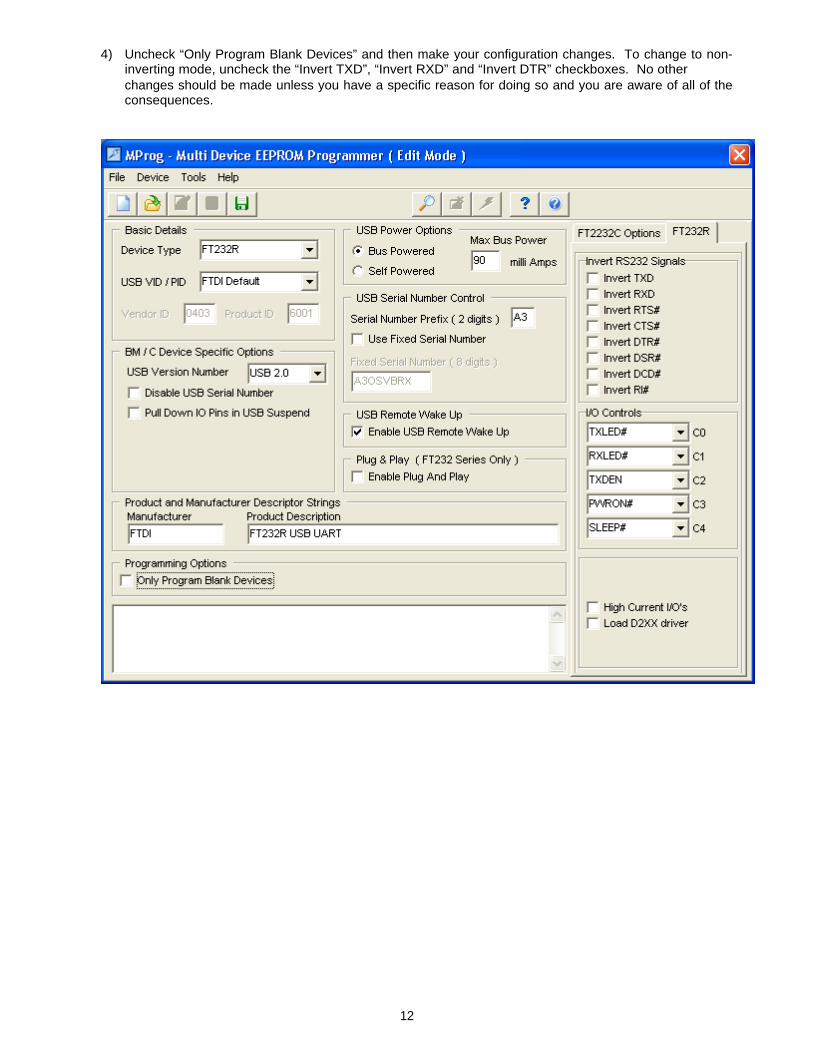
4) Uncheck “Only Program Blank Devices” and then make your configuration changes. To change to non-inverting mode, uncheck the “Invert TXD”, “Invert RXD” and “Invert DTR” checkboxes. No other changes should be made unless you have a specific reason for doing so and you are aware of all of the consequences.
13
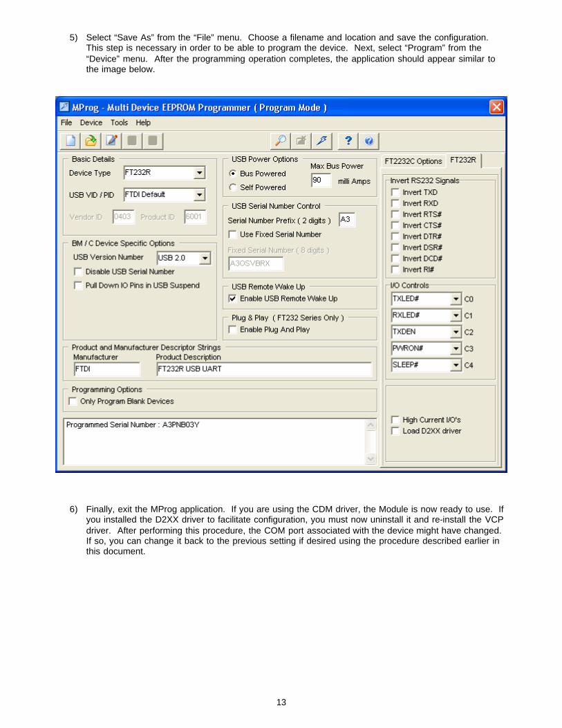
5) Select “Save As” from the “File” menu. Choose a filename and location and save the configuration. This step is necessary in order to be able to program the device. Next, select “Program” from the “Device” menu. After the programming operation completes, the application should appear similar to the image below.
6) Finally, exit the MProg application. If you are using the CDM driver, the Module is now ready to use. If you installed the D2XX driver to facilitate configuration, you must now uninstall it and re-install the VCP driver. After performing this procedure, the COM port associated with the device might have changed. If so, you can change it back to the previous setting if desired using the procedure described earlier in this document.

14
Schematic
A larger version of this schematic is available at http://www.zbasic.net/doc/USB-TTL/schematic.jpg.