Embed Size (px)
Citation preview

University of Groningen
Device physics of organic bulk heterojunction solar cellsMihailetchi, V.D
IMPORTANT NOTE: You are advised to consult the publisher's version (publisher's PDF) if you wish to cite fromit. Please check the document version below.
Document VersionPublisher's PDF, also known as Version of record
Publication date:2005
Link to publication in University of Groningen/UMCG research database
Citation for published version (APA):Mihailetchi, V. D. (2005). Device physics of organic bulk heterojunction solar cells s.n.
CopyrightOther than for strictly personal use, it is not permitted to download or to forward/distribute the text or part of it without the consent of theauthor(s) and/or copyright holder(s), unless the work is under an open content license (like Creative Commons).
Take-down policyIf you believe that this document breaches copyright please contact us providing details, and we will remove access to the work immediatelyand investigate your claim.
Downloaded from the University of Groningen/UMCG research database (Pure): http://www.rug.nl/research/portal. For technical reasons thenumber of authors shown on this cover page is limited to 10 maximum.
Download date: 05-06-2018

Device Physics of Organic BulkHeterojunction Solar Cells
Valentin Dan Mihailet, chi

MSC Ph.D.-thesis series 2005-14ISSN 1570-1530
The work described in this thesis was performed in the research group Physicsof Organic Semiconductors of the Materials Science Centre at the Universityof Groningen, The Netherlands. The project was financially supported by theDutch government through the E.E.T. program (EETK97115).
PUBLISHED BY: Valentin Dan Mihailet, chi
PRINTED BY: Drukkerij van Denderen B.V., Groningen, The Netherlands
Copyright c© 2005 by Valentin Dan Mihailet, chi

RIJKSUNIVERSITEIT GRONINGEN
Device Physics of Organic BulkHeterojunction Solar Cells
Proefschrift
ter verkrijging van het doctoraat in deWiskunde en Natuurwetenschappenaan de Rijksuniversiteit Groningen
op gezag van deRector Magnificus, dr. F. Zwarts,in het openbaar te verdedigen op
maandag 14 november 2005om 13.15 uur
door
Valentin Dan Mihailet, chi
geboren op 30 september 1974
te Timis, oara

Promotor: Prof. dr. ir. P. W. M. Blom
Beoordelingscommissie: Prof. dr. J. C. HummelenProf. dr. ir. R. A. J. JanssenProf. dr. M. D. McGehee
ISBN 90-367-2393-0

Contents
1 Introduction 11.1 Motivation . . . . . . . . . . . . . . . . . . . . . . . . . . . . . . . . 2
1.1.1 Inorganic solar cells . . . . . . . . . . . . . . . . . . . . . . 21.1.2 Organic solar cells . . . . . . . . . . . . . . . . . . . . . . . 3
1.2 Outline of the thesis . . . . . . . . . . . . . . . . . . . . . . . . . . . 91.3 Abbreviations . . . . . . . . . . . . . . . . . . . . . . . . . . . . . . 10References . . . . . . . . . . . . . . . . . . . . . . . . . . . . . . . . . . . 11
2 Charge transport in polymer:fullerene films 152.1 Photoconduction in insulators . . . . . . . . . . . . . . . . . . . . . 162.2 Electron transport in fullerene films . . . . . . . . . . . . . . . . . 18
2.2.1 Introduction . . . . . . . . . . . . . . . . . . . . . . . . . . . 182.2.2 Results and Discussion . . . . . . . . . . . . . . . . . . . . . 192.2.3 Conclusion . . . . . . . . . . . . . . . . . . . . . . . . . . . 22
2.3 Electron and hole transport in polymer:fullerene blends . . . . . . 222.3.1 Introduction . . . . . . . . . . . . . . . . . . . . . . . . . . . 222.3.2 Electron transport in polymer:fullerene films . . . . . . . . 242.3.3 Hole transport in polymer:fullerene films . . . . . . . . . . 252.3.4 Conclusion . . . . . . . . . . . . . . . . . . . . . . . . . . . 34
2.4 Experimental section . . . . . . . . . . . . . . . . . . . . . . . . . . 34References . . . . . . . . . . . . . . . . . . . . . . . . . . . . . . . . . . . 36
3 Photocurrent generation in bulk heterojunction solar cells 393.1 Photocurrent in polymer:fullerene blends . . . . . . . . . . . . . . 40
3.1.1 Introduction . . . . . . . . . . . . . . . . . . . . . . . . . . . 403.1.2 Photocurrent-voltage characteristics . . . . . . . . . . . . . 403.1.3 The origin of the field-dependent (reverse bias) photocurrent 413.1.4 A model for charge carriers dissociation at donor/acceptor
interface . . . . . . . . . . . . . . . . . . . . . . . . . . . . . 433.1.5 Comparing the model with the experimental photocurrent 443.1.6 Conclusion . . . . . . . . . . . . . . . . . . . . . . . . . . . 46
3.2 Space-charge limitation in organic solar cells . . . . . . . . . . . . 463.2.1 Introduction . . . . . . . . . . . . . . . . . . . . . . . . . . . 463.2.2 Goodman and Rose approximation . . . . . . . . . . . . . 473.2.3 Experimental evidence . . . . . . . . . . . . . . . . . . . . . 48
v

vi CONTENTS
3.2.4 Analytical prediction for the conversion efficiency . . . . . 523.2.5 Conclusion . . . . . . . . . . . . . . . . . . . . . . . . . . . 53
3.3 Experimental section . . . . . . . . . . . . . . . . . . . . . . . . . . 53References . . . . . . . . . . . . . . . . . . . . . . . . . . . . . . . . . . . 55
4 Variation of the metal top electrode in bulk heterojunction solar cells 574.1 Electrode dependence of the open-circuit voltage . . . . . . . . . . 58
4.1.1 Introduction . . . . . . . . . . . . . . . . . . . . . . . . . . . 584.1.2 Open-circuit voltage of pristine fullerene devices . . . . . 594.1.3 Open-circuit voltage of polymer:fullerene devices . . . . . 644.1.4 Conclusion . . . . . . . . . . . . . . . . . . . . . . . . . . . 67
4.2 Effect of metal electrodes on solar cell performance . . . . . . . . 684.2.1 Introduction . . . . . . . . . . . . . . . . . . . . . . . . . . . 684.2.2 Results and discussion . . . . . . . . . . . . . . . . . . . . . 694.2.3 Conclusion . . . . . . . . . . . . . . . . . . . . . . . . . . . 71
4.3 Experimental section . . . . . . . . . . . . . . . . . . . . . . . . . . 71References . . . . . . . . . . . . . . . . . . . . . . . . . . . . . . . . . . . 73
5 Compositional dependence of the performance in polymer:fullerenecells 755.1 Introduction . . . . . . . . . . . . . . . . . . . . . . . . . . . . . . . 765.2 Compositional dependence of the charge-carrier mobility . . . . . 765.3 Device characterization under illumination . . . . . . . . . . . . . 805.4 Conclusion . . . . . . . . . . . . . . . . . . . . . . . . . . . . . . . . 855.5 Experimental section . . . . . . . . . . . . . . . . . . . . . . . . . . 86References . . . . . . . . . . . . . . . . . . . . . . . . . . . . . . . . . . . 87
6 Exploring poly(3-hexylthiophene):fullerene solar cells 896.1 Introduction . . . . . . . . . . . . . . . . . . . . . . . . . . . . . . . 906.2 Charge carrier transport in composite P3HT:PCBM films . . . . . 916.3 Optical absorption spectra . . . . . . . . . . . . . . . . . . . . . . . 956.4 Device characterization under illumination . . . . . . . . . . . . . 97
6.4.1 The effect of thermal annealing on solar cell performance . 976.4.2 Light intensity dependence . . . . . . . . . . . . . . . . . . 1006.4.3 Numerical simulation results . . . . . . . . . . . . . . . . . 102
6.5 Conclusion . . . . . . . . . . . . . . . . . . . . . . . . . . . . . . . . 1056.6 Experimental section . . . . . . . . . . . . . . . . . . . . . . . . . . 105References . . . . . . . . . . . . . . . . . . . . . . . . . . . . . . . . . . . 107
Summary 109
Samenvatting 113
List of Publications 117
Acknowledgements 119
1Introduction
Abstract
As the evidence of global warming continues to build-up, it is becoming clearthat we will have to find ways to produce electricity without the release of car-bon dioxide and other greenhouse gases. Fortunately, we have renewable en-ergy sources which neither run out nor have any significant harmful effects onour environment. Harvesting energy directly from the sunlight using photo-voltaic (PV) technology is being widely recognized as an essential componentof future global energy production. In this chapter, a brief overview regard-ing the photovoltaic devices is given, with emphasis on the organic solar cells,ending with a short outline of the thesis.
1

2 Chapter 1: Introduction
1.1 Motivation
As the global energy demand continues to increase every year, the limiting sup-ply of today’s main energy sources (i.e. oil, coal, uranium) and their detrimentallong-term effects on the natural balance on our planet, underscore the urgencyof developing renewable energy sources. Today’s plants are unable to absorb thehuge amount of extra carbon dioxide that is released in the earth’s atmospheremainly by burning of fossil fuel [1, 2]. As a result, the increased concentrationof carbon dioxide in the atmosphere considerably adds to the greenhouse effectwhich will increase the global mean surface temperature [2]. The consequenceof these chances are already seen by an increase in the frequency and severity ofnatural disasters [1].
Fortunately, we have renewable energy sources which neither run out norhave any significant harmful effects on the environment. Harvesting energydirectly from the sunlight using photovoltaic (PV) technology is being widelyrecognized as an essential component of future global energy production. Pro-vided that PV devices can be made truly economically competitive with fossilfuels and other emerging renewable energy technologies, large scale manufac-turing of these devices offers a sustainable energy source which can supply asignificant fraction of our daily energy needs.
1.1.1 Inorganic solar cells
The photovoltaic cells have become extensively studied since the 1950s when thefirst crystalline silicon solar cell, which had an efficiency of 6%, was developedat Bell Laboratories [3]. Since then, the efficiency has reached 24% for crystallineSi solar cells [4], which is already close to the theoretical predicted upper limit of30% [5, 6]. Practically all conventional inorganic solar cells incorporate a semi-conductor that is doped to form a p-n junction across which the photovoltageis generated. The p side contains an excess of the positive charges (holes), andthe n side contains an excess of the negative charges (electrons). In the regionnear the junction an electric field is formed and the electrons and holes, whichare generated through light absorption in the bulk of Si, diffuse to this junction,where they are directed by the electric field towards the proper electrode. Overthe years, solar cells have been made from many other semiconductor materi-als with various device configuration such as single-crystal, polycrystalline, andamorphous thin-film structures. At present, crystalline Si solar cells are by farmost dominant PVs used and account for more than 85% of the market. A com-prehensive review on Si and other type of solar cells can be found in literature[7].
Although in the last 5 years the production of PV modules was increasedsteadily by an annual average of 40%, the semiconductor PV still accounts forless that 0.1% of the total world energy production. One of the major obstaclesfor the market implementation of PV cells is the large production costs for Si-based technology. However, despite much effort of further reducing the price,large scale production of Si-based solar cells will be limited by the availabilityof raw materials, such as solar-grade Si. Therefore, to ensure a sustainable tech-

1.1. Motivation 3
nology path for PV, the development of new materials and device structures arerequired.
1.1.2 Organic solar cells
Organic materials bear the potential to develop a long-term technology that iseconomically viable for large-scale power generation based on environmentallysafe materials with unlimited availability. Organic semiconductors are a lessexpensive alternative to inorganic semiconductors like Si; they can have ex-tremely high optical absorption coefficients which offer the possibility for theproduction of very thin solar cells. Additional attractive features of organic PVsare the possibilities for thin flexible devices which can be fabricated using high-throughput, low temperature approaches that employ well established printingtechniques in a roll-to-roll process [8, 9]. This possibility of using flexible plas-tic substrates in an easily scalable high-speed printing process can reduce thebalance of system cost for organic PVs, resulting in a shorter energetic pay-backtime.
The electronic structure of all organic semiconductors is based on conjugatedπ-electrons. A conjugated organic system is made of an alternation between sin-gle and double carbon-carbon bonds. Single bonds are known as σ-bonds andare associated with localized electrons, and double bonds contain a σ-bond anda π-bond. The π-electrons are much more mobile than the σ-electrons; they canjump from site to site between carbon atoms thanks to the mutual overlap ofπ-orbitals along the conjugation path, which causes the wave functions to delo-calize over the conjugated backbone. The π-bands are either empty (called theLowest Unoccupied Molecular Orbital - LUMO) or filled with electrons (calledthe Highest Occupied Molecular Orbital - HOMO). The band gap of these mate-rials ranges from 1 to 4 eV. This π-electron system has all the essential electronicfeatures of organic materials: light absorption and emission, charge generationand transport. Figure 1.1 shows several examples of conjugated organic moi-eties.
A typical organic PV cell consists of a photoactive layer sandwiched between
(e) PCBM
nnO
O
n
O
OMe
nS
(d) P3HT(c) MDMO-PPV(b) PPV(a) PA
Figure 1.1: Chemical structures and abbreviations of some conjugated organic molecules.
From left: poly(acetylene) PA, poly(para-phenylene-vinylene) PPV, a substituted PPV
(MDMO-PPV), poly(3-hexyl thiophene) P3HT, and a C60 derivative ([60]PCBM, called
PCBM throughout this thesis). In each compound one can identify a sequence of alter-
nating single and double bonds.
4 Chapter 1: Introduction
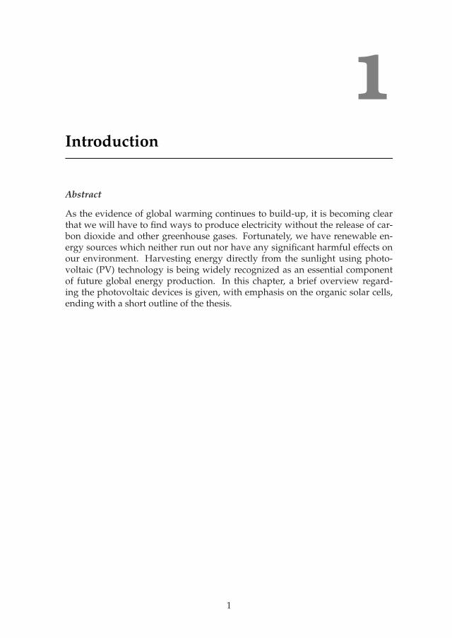
Figure 1.2: Schematic layout of an organic solar cell.
two different electrodes, one of which should be transparent in order to allowthe incoming photons to reach the photoactive layer, as seen in Figure 1.2. Thisphotoactive layer is based on a single, a bi-layer, or a mixture of two (or more)components. Upon light absorption the charge carriers are generated inside thephotoactive layer and due to the presence of an electric field, provided by theasymmetrical ionization energies/work functions of the electrodes (anode andcathode)∗, these charges are transported and collected into the external circuit.In this way an organic solar cell converts light into electricity.
The first investigation of an organic PV cell came as early as 1959, when ananthracene single crystal was studied. The cell exhibited a photovoltage of 200mV with an extremely low efficiency [10]. Since then, many years of researchhave shown that the typical power conversion efficiency of PV devices basedon single (or homojunction) organic materials will remain below 0.1%, makingthem unsuitable for any possible application. Primarily, this is due to the factthat absorption of light in organic materials almost always results in the produc-tion of a mobile excited state (referred to as exciton), rather than free electron-hole pairs as produced in inorganic solar cells. This occurs for the reason that or-ganic materials are characterized by low dielectric constant (typically 2-4), com-pared to inorganic semiconductors, which require an energy input much higherthan the thermal energy (kT ) to dissociate these excitons [11–13]. The electricfield provided by the asymmetrical work functions of the electrodes is not suf-ficient to break-up these photogenerated excitons. Instead, the excitons diffusewithin the organic layer until they reach the electrode, where they may dissoci-ate to supply separate charges, or recombine. Since the exciton diffusion lengthsare typically 1-10 nm [14–18], being much shorter than the device thicknesses,exciton diffusion limits charge carrier generation in these devices since most ofthem are lost through recombination. Photogeneration is therefore a functionof the available mechanisms for excitons dissociation. A major breakthrough inthe cell performance came in 1986 when Tang discovered that much higher effi-ciencies (about 1%) are attainable when bringing an electron donor (D) and anelectron acceptor (A) together in one cell [19]. This concept of heterojunction is
∗Herein the anode was taken as the positively biased electrode and the cathode as the negativelybiased electrode.

1.1. Motivation 5
the heart of all three currently existing types of organic PV cells: dye-sensitizedsolar cells [20–22]; planar organic semiconductor cells [19, 23–25]; and high sur-face area, or bulk heterojunction cells [8, 26–28]. In the following this conceptis briefly reviewed together with the operation processes and limitations of theorganic PV cell.
The concept of an organic (bulk) heterojunction
Most of the developments that have improved the performance of organic PVdevices are based on D/A heterojunctions. The idea behind a heterojunction isto use two materials with different electron affinities and ionization potentials.At the interface, the resulted potentials are strong and may favor exciton dis-sociation: the electron will be accepted by the material with the larger electronaffinity and the hole by the material with the lower ionization potential, pro-vided that the differences in potential energy are larger than the exciton bindingenergy. In the planar heterojunction, or ’bi-layer’ device, the organic D/A inter-face separates excitons much more efficient than an organic/metal interface inthe single layer device. The energetic diagram of such a bi-layer device is de-picted in the Figure 1.3(a). Sunlight photons which are absorbed inside the de-vice excite the donor molecule (1), leading to the creation of excitons. However,the acceptor phase can also absorb light, but for simplicity only the photons thatare absorbed by the donor phase are considered here. The created excitons startto diffuse (3) within the donor phase and if they encounter the interface withthe acceptor then a fast dissociation takes place (4) leading to charge separation[29, 30]. The resulting metastable electron-hole pairs across the D/A interfacemay still be Coulombically bound and an electric field is needed to separatethem into free charges [31, 32]. Therefore, at typical operation conditions, thephoton-to-free-electron conversion efficiency is not maximal. Subsequently, theseparated free electrons (holes) are transported (5) with the aid of the internalelectric field, caused by the use of electrodes with different work functions, to-wards the cathode (anode) where they are collected by the electrodes (6) anddriven into the external circuit. However, the excitons can decay (2), yieldinge.g. luminescence, if they are generated far from the interface. Thus, the ex-citons should be formed within the diffusion length of the interface. Since theexciton diffusion lengths in organic materials are much shorter than the absorp-tion depth of the film, this limits the width of effective light-harvesting layer.
A revolutionary development in organic PVs came in the mid 1990s with theintroduction of the dispersive (or bulk) heterojunction, where the donor and ac-ceptor material are blended together. If the length scale of the blend is similarto the exciton diffusion length, the exciton decay processes (2) is dramaticallyreduced since in the proximity of every generated exciton there is an interfacewith an acceptor where fast dissociation takes place (4). Hence, charge genera-tion takes place everywhere in the active layer, as is schematically representedin Figure 1.3(b). Provided that continuous pathways exist in each material fromthe interface to the respective electrodes, the photon-to-electron conversion ef-ficiency and, hence, the photosensitivity is dramatically increased. The obser-vation of improved device performance using bulk heterojunctions represents

6 Chapter 1: Introduction
Figure 1.3: Schematic band diagram of a bi-layer device (a) and a bulk heterojunction
(b). The numbers refer to the operation processes explained in the text. The dashed line
represents the energy levels of the acceptor, while the full lines indicate the energy level
of the donor in the PV cell.
the departure from the device physics of conventional inorganic PV cells andhas led to new device and materials designs. Nowadays, the bulk heterojunc-tion is the most promising concept for all-organic PV cells. Dye-sensitized solarcells, as developed in 1990s by Gratzel, however, function on similar principles[20–22].
One class of organic materials used as photoactive layer in bulk heterojunc-tion PV cells that have received considerable attention in the last few years aresemiconducting polymers and molecules. They combine the opto-electronicproperties of conventional semiconductors with the excellent mechanical andprocessing properties of ’plastic’ materials. Additionally, they possess an un-precedented flexibility in the synthesis, allowing for alteration of a wide rangeof properties, such as bandgap, molecular orbital energy level, wetting andstructural properties, as well as doping. This ability to design and synthesizepolymers and molecules that can be casted from solution using wet-processingtechniques such as spin-coating, ink jet printing, and screen printing, representsan enormous attractive route for cheap production of large-area PV cells thatcan be applied to systems that require flexible substrates. Since ultrafast pho-toinduced electron transfer from a conjugated polymer as donor to buckmin-sterfullerene (C60) or its derivatives as acceptor was first observed in 1992 bySariciftci et al. [29], this material combination has been extensively studied inbulk heterojunction PV cells. In 1995 Yu et al. [27] fabricated the first fully or-ganic bulk heterojunction cell based on a mixture of soluble PPV derivative witha fullerene acceptor [such as C60 derivative PCBM [33]; Figure 1.1(e)]. In 2001Shaheen et al. [34] obtained the first truly promising results for bulk heterojunc-tion solar cells when mixing a conjugated polymer [such as MDMO-PPV, Figure1.1(c)] with PCBM in a 20:80 weight percentage and optimizing the nanoscalemorphology of the film, yielding a power conversion efficiency of 2.5%. Re-cently, power conversion efficiencies of >3.5% have been achieved for poly-mer:fullerene (PCBM) bulk heterojunction solar cells based on polythiophenederivatives [such as regioregular P3HT; Figure 1.1(d)] as absorbing and electron-

1.1. Motivation 7
Jph Jmax
Vmax
VOC
Cur
rent
den
sity
/J
Voltage/ V
Pmax
JSC
Figure 1.4: Typical J-V characteristics of an organic PV cell in the dark (dashed line)
and illumination (solid line) conditions. The short-circuit current density (JSC ) and
open-circuit voltage (VOC ) are shown. The maximum output power (Pmax) is given by
the rectangle Jmax×Vmax.
donating material [35–39].
Characterization of organic bulk heterojunction PV cells
Bulk heterojunction solar cells with a photoactive layer prepared from a conju-gated polymer and fullerene molecules, are fabricated by depositing (i.e. spin-coating) the active layer from a solution on a transparent bottom electrode, nor-mally indium-tin-oxide (ITO), which forms the anode. To enhance the repro-ducibility and the performance of the devices, a thin conductive organic layeris typically applied from solution on top of ITO, before the actual active layeris deposited. The most widely used cover layer on ITO is a transparent com-posite PEDOT:PSS [40–42], consisting of oxidized polyethylenedioxythiophene(PEDOT) and impartially anionic form polystyrenesulfonate (PSS). A low workfunction metal (calcium, barium, or a thin layer of lithium fluoride; all topedwith aluminum) is evaporated under high vacuum on top of the photoactivelayer and serves as cathode, as shown schematically in Figure 1.2. Under illumi-nation (at short-circuit condition), the main processes that govern the operationof these devices are depicted in Figure 1.3(b).
In order to investigate the PV performance of a cell, as well as its electric be-havior, the current density-voltage (J-V ) characteristics in the dark and underillumination are considered. Figure 1.4 shows a typical J-V curve of a PV devicein the dark (dashed line) and under illumination (solid line). When the cell isilluminated, the J-V curve is shifted down by the amount of photocurrent (Jph)generated. The open-circuit voltage, VOC , is the maximum photovoltage thatcan be generated in the cell and corresponds to the voltage where current underillumination is zero. The maximum current that can run through the cell at zeroapplied voltage is called the short-circuit current, JSC . The maximum of the ob-tained electrical power Pmax is located in the fourth quadrant where the productof current density J and voltage V reached its maximum value (Jmax×Vmax; as

8 Chapter 1: Introduction
seen in Figure 1.4). It is observed from the Figure 1.4 that Pmax is bigger whenthe J-V curve resembles a rectangular with the area JSC×VOC . The ratio be-tween (the rectangle of) Pmax and the product of (or a rectangle defined by) JSC
and VOC measures the quality of the shape of the J-V characteristics, and isdefined as the fill factor (FF):
FF ≡ Jmax · Vmax
JSC · VOC, (1.1)
thus Pmax=JSC ·VOC ·FF. The power conversion efficiency η of a solar cell is theratio between the maximum output power Pmax and the power of the incidentlight Plight:
η ≡ Pmax
Plight=
JSC · VOC · FF
Plight. (1.2)
Because of the wavelength and intensity dependence of Pmax, the power conver-sion efficiency η should be measured under standard test conditions∗. Equation1.2 shows that in order to increase η, for the same incident light power Plight,either JSC , VOC , or FF (or all) need to be increased. For organic solar cells basedon polymer:fullerene bulk heterojunctions, the magnitude of JSC , VOC , and FFdepends on parameters such as: light intensity [43], temperature [44, 45], com-position of the components [46], thickness of the active layer [47], the choiceof electrodes used [48, 49], as well as the solid state morphology of the film[34]. Their optimization and maximization require a clear understanding of thedevice operation and photocurrent, Jph, generation and its limitations in thesedevices. The relation between the experimental Jph and material parameters(i.e., charge-carrier mobility, bandgap, molecular energy levels, or relative di-electric constant) needs to be understood and controlled in order to allow forfurther design of new materials that can improve the efficiency of this type ofsolar cells.
A first attempt to understand the physics behind the organic bulk hetero-junction solar cells was done by using numerical models and concepts that arewell established for inorganic solar cells, such as the p-n junction model. Toimprove the agreement of the classical p-n model with the experimental Jph ofan organic bulk heterojunction cell, an expanded replacement circuit has beenintroduced [38, 50, 51]. This model replaces the photoactive layer by an idealdiode and a serial and a parallel resistance, which have an ambiguous physicalmeaning for an organic cell. However, different to classical p-n junction cellswith spatially separated p- and n-type regions of doped semiconductors, bulkheterojunction cells consist of an intimate mixture of two un-doped (intrinsic)semiconductors that are nanoscopically mixed and that generate a randomlyoriented interface. Moreover, due to the different charge generation, transportand recombination processes in bulk heterojunctions, the classical p-n junction
∗To allow meaningful comparisons of solar cell performances all over the world, the PV cells arerated at a well-defined set of conditions known as Standard Test Conditions (STC). These conditionsinclude the temperature of the PV cells (25 oC), the intensity of radiation (1000 W/m2), and thespectral distribution of the light (air mass 1.5 or AM1.5, which is the spectrum of sunlight that hasbeen filtered by passing through 1.5 thicknesses of the earth’s atmosphere).

1.2. Outline of the thesis 9
model is not applicable to describe the Jph of these solar cells [52]. An alter-native approach is to use the metal-insulator-metal (MIM) concept [28], wherea homogenous blend of two unipolar semiconductors (donor/acceptor) is de-scribed as one semiconductor with properties derived from the two materials.This means that the photoactive layer is described as one ’virtual’ semiconduc-tor assuming that its conduction band is given by the LUMO of the acceptorand its valence band is determined by the HOMO of the donor-type material[see Figure 1.3(b)]. Under PV operation mode (at short-circuit condition), thepotential difference available in the MIM device, that drives the photogener-ated charge carriers towards the collection electrodes, is caused by the differencebetween the work functions of the metal electrodes. The applicability of MIMmodel to organic bulk heterojunction cells is demonstrated through the workpresented in this thesis.
1.2 Outline of the thesis
In 2001 bulk heterojunction solar cells prepared from conjugated polymers andfullerene molecules made a significant step in power conversion efficiency from1% to 2.5%. Despite this enhancement, resulting mostly from an improved solidstate morphology of the film, there was not much known about charge transportand photogeneration mechanisms that govern the efficiency of these type of PVcells. Questions that need to be answered are: what are the charge-carrier mobil-ities in the polymer, fullerene, and in their mixture? How efficient and throughwhich mechanisms do the charge carriers dissociate at the polymer/fullerene in-terface? What is the role of the electrodes, or what limits the efficiency at lowerfullerene fractions? This thesis discusses and underlines the fundamental pro-cesses behind the operation of these solar cells, which are absolutely necessaryto further improve the device performance.
To understand the photocurrent generation in bulk heterojunction solar cellsbased on conjugated polymer and fullerene molecules, in Chapter 2 the transportof charge carriers in the pristine fullerene and polymer:fullerene films is inves-tigated and interpreted, using a phenomenological model for the charge carriermobility. The experimental results for charge carrier mobilities are further dis-cussed on the basis of energetic disorder of the system and molecular packingof the components in the film.
The photocurrent generation in polymer:fullerene blends is discussed inChapter 3, with emphasis on the mechanism of charge dissociation at the poly-mer/fullerene interface and the consequences that an unbalanced transport ofelectrons and holes has on the photocurrent and device performance. A funda-mental electrostatic limit for the photocurrent in the polymer:fullerene blends isdiscussed and experimentally proved.
The metal electrode dependence of the performance of polymer:fullerene so-lar cells is treated in Chapter 4. First, the open-circuit voltage of the solar cell isinvestigated by using metal electrodes with different work functions. A relationbetween open-circuit voltage and metal work function is established. Subse-quently, the effect of metal work function on other solar cell parameters, such as

10 Chapter 1: Introduction
short-circuit current, fill factor, and maximum output power, is discussed.In Chapter 5, the dependence of the performance of polymer:fullerene cells
on their composition is addressed. The charge carrier mobilities of electronsand holes, as a function of fullerene fraction, is measured independently in theblend using the current-voltage technique. The obtained mobilities are usedto study the photocurrent in these blends, as a function of their composition,and identify the parameters that limit the device performance at lower fullerenefractions where light absorption is more effective.
Finally, Chapter 6 describes the charge transport and photocurrent gener-ation in composite films of regioregular poly(3-hexylthiophene) and PCBMmolecules. The improved performance by applying a post production heat treat-ment to the devices is discussed in terms of charge carrier mobility, optical ab-sorption spectroscopy, and photocurrent generation.
1.3 Abbreviations
For clarity, we have used abbreviations which are most common in the field. Ta-ble 1.1 summarizes the most common abbreviations used throughout this thesis.
Table 1.1: List of most common abbreviations used throughout the thesis.
AM1.5 Air mass 1.5BEHBMB-PPV Poly[(2,5-bis(2’-ethylhexyloxy))-co-(2,5-bis(2’-
methylbutyloxy))-para-phenylenevinylene]BHJ Bulk heterojunctionFF Fill factorG Generation rate of bound electron-hole pairsHOMO Highest occupied molecular orbitalITO Indium-tin-oxideJD Current density in the darkJL Current density under illuminationJph Net photocurrentJSC Short-circuit currentLUMO Lowest unoccupied molecular orbitalMDMO-PPV Poly(2-methoxy-5-(3‘,7‘-dimethyloctyloxy)-para-
phenylene vinylene)P3HT regioregular Poly(3-hexylthiophene)PCBM Phenyl-C61-butyric acid methyl esterPEDOT:PSS Polyethylenedioxythiophene:polystyrenesulfonatePPV Poly(para-phenylene vinylene)V0 Compensation voltageVBI Built-in voltageVRS Voltage drop on series resitanceVOC Open-circuit voltage

REFERENCES 11
References
[1] United Nations Environment Programme (UNEP), Global environment outlook (GEOyear book 2004/5), Web site: www.unep.org/geo/yearbook.
[2] Intergovernmental Panel on Climate Changes (IPCC), Third assessment report - cli-mate changes 2001, Web site: www.meto.gov.uk.
[3] D. M. Chapin, C. S. Fuller, G. L. Pearson, A new silicon p-n junction photocell for con-verting solar radiation into electrical power, Journal of Applied Physics 25 (1954), 676.
[4] M. A. Green, K. Emery, D. L. King, S. Igari, W. Warta, Solar cell efficiency tables (version25), Progress in Photovoltaics 13 (2005), 49.
[5] W. Shockley, H. J. Queisser, Detailed balance limit of efficiency of p-n junction solar cells,Journal of Applied Physics 32 (1961), 510.
[6] M. A. Green, Solar cells - Operating principles, technology and system applications, Uni-versity of New South Wales, Sydney, (1992).
[7] A. Goetzberger, C. Hebling, H. W. Schock, Photovoltaic materials, history, status andoutlook, Materials Science & Engineering R-Reports 40 (2003), 1.
[8] S. E. Shaheen, R. Radspinner, N. Peyghambarian, G. E. Jabbour, Fabrication of bulkheterojunction plastic solar cells by screen printing, Applied Physics Letters 79 (2001),2996.
[9] G. Gustafsson, Y. Cao, G. M. Treacy, F. Klavetter, N. Colaneri, A. J. Heeger, Flexiblelight-emitting-diodes made from soluble conducting polymers, Nature 357 (1992), 477.
[10] H. Kallmann, M. Pope, Photovoltaic effect in organic crystals, Journal of ChemicalPhysics 30 (1959), 585.
[11] S. Barth, H. Bassler, Intrinsic photoconduction in PPV-type conjugated polymers, Physi-cal Review Letters 79 (1997), 4445.
[12] P. G. Dacosta, E. M. Conwell, Excitons and the band-gap in poly(phenylene vinylene),Physical Review B 48 (1993), 1993.
[13] R. N. Marks, J. J. M. Halls, D. D. C. Bradley, R. H. Friend, A. B. Holmes, The pho-tovoltaic response in poly(p-phenylene vinylene) thin-film devices, Journal of Physics-Condensed Matter 6 (1994), 1379.
[14] V. Choong, Y. Park, Y. Gao, T. Wehrmeister, K. Mullen, B. R. Hsieh, C. W. Tang,Dramatic photoluminescence quenching of phenylene vinylene oligomer thin films uponsubmonolayer ca deposition, Applied Physics Letters 69 (1996), 1492.
[15] J. J. M. Halls, K. Pichler, R. H. Friend, S. C. Moratti, A. B. Holmes, Exciton diffu-sion and dissociation in a poly(p-phenylenevinylene)/C-60 heterojunction photovoltaic cell,Applied Physics Letters 68 (1996), 3120.
[16] J. J. M. Halls, R. H. Friend, The photovoltaic effect in a poly(p-phenylenevinylene)/peryleneheterojunction, Synthetic Metals 85 (1997), 1307.
[17] D. E. Markov, E. Amsterdam, P. W. M. Blom, A. B. Sieval, J. C. Hummelen, Accuratemeasurement of the exciton diffusion length in a conjugated polymer using a heterostruc-ture with a side-chain cross-linked fullerene layer, Journal of Physical Chemistry A 109(2005), 5266.
[18] D. E. Markov, C. Tanase, P. W. M. Blom, J. Wildeman, Simultaneous enhancement of thecharge transport and exciton diffusion in poly(p-phenylene vinylene) derivatives, Physical
12 Chapter 1: Introduction
Review B 72 (2005), 045217.
[19] C. W. Tang, Two-layer organic photovoltaic cell, Applied Physics Letters 48 (1986), 183.
[20] M. Gratzel, Photoelectrochemical cells, Nature 414 (2001), 338.
[21] B. O’Regan, M. Gratzel, A low-cost, high-efficiency solar-cell based on dye-sensitized col-loidal TiO2 films, Nature 353 (1991), 737.
[22] A. K. Jana, Solar cells based on dyes, Journal of Photochemistry and PhotobiologyA-Chemistry 132 (2000), 1.
[23] P. Peumans, V. Bulovic, S. R. Forrest, Efficient photon harvesting at high optical in-tensities in ultrathin organic double-heterostructure photovoltaic diodes, Applied PhysicsLetters 76 (2000), 2650.
[24] B. A. Gregg, Bilayer molecular solar cells on spin-coated TiO2 substrates, ChemicalPhysics Letters 258 (1996), 376.
[25] M. Granstrom, K. Petritsch, A. C. Arias, A. Lux, M. R. Andersson, R. H. Friend,Laminated fabrication of polymeric photovoltaic diodes, Nature 395 (1998), 257.
[26] J. J. M. Halls, C. A. Walsh, N. C. Greenham, E. A. Marseglia, R. H. Friend, S. C.Moratti, A. B. Holmes, Efficient photodiodes from interpenetrating polymer networks, Na-ture 376 (1995), 498.
[27] G. Yu, J. Gao, J. C. Hummelen, F. Wudl, A. J. Heeger, Polymer photovoltaic cells -enhanced efficiencies via a network of internal donor-acceptor heterojunctions, Science 270(1995), 1789.
[28] C. J. Brabec, N. S. Sariciftci, J. C. Hummelen, Plastic solar cells, Advanced FunctionalMaterials 11 (2001), 15.
[29] N. S. Sariciftci, L. Smilowitz, A. J. Heeger, F. Wudl, Photoinduced electron-transfer froma conducting polymer to buckminsterfullerene, Science 258 (1992), 1474.
[30] C. J. Brabec, G. Zerza, G. Cerullo, S. De Silvestri, S. Luzzati, J. C. Hummelen, S. Sari-ciftci, Tracing photoinduced electron transfer process in conjugated polymer/fullerene bulkheterojunctions in real time, Chemical Physics Letters 340 (2001), 232.
[31] C. L. Braun, Electric-field assisted dissociation of charge-transfer states as a mechanism ofphotocarrier production, Journal of Chemical Physics 80 (1984), 4157.
[32] T. E. Goliber, J. H. Perlstein, Analysis of photogeneration in a doped polymer system interms of a kinetic-model for electric-field-assisted dissociation of charge-transfer states, Jour-nal of Chemical Physics 80 (1984), 4162.
[33] J. C. Hummelen, B. W. Knight, F. Lepeq, F. Wudl, J. Yao, C. L. Wilkins, Prepara-tion and characterization of fulleroid and methanofullerene derivatives, Journal of OrganicChemistry 60 (1995), 532.
[34] S. E. Shaheen, C. J. Brabec, N. S. Sariciftci, F. Padinger, T. Fromherz, J. C. Hummelen,2.5% efficient organic plastic solar cells, Applied Physics Letters 78 (2001), 841.
[35] D. Chirvase, J. Parisi, J. C. Hummelen, V. Dyakonov, Influence of nanomorphology onthe photovoltaic action of polymer-fullerene composites, Nanotechnology 15 (2004), 1317.
[36] Y. Kim, S. A. Choulis, J. Nelson, D. D. C. Bradley, S. Cook, J. R. Durrant, Deviceannealing effect in organic solar cells with blends of regioregular poly(3-hexylthiophene)and soluble fullerene, Applied Physics Letters 86 (2005), 063502.
[37] F. Padinger, R. S. Rittberger, N. S. Sariciftci, Effects of postproduction treatment on plas-tic solar cells, Advanced Functional Materials 13 (2003), 85.
REFERENCES 13
[38] C. J. Brabec, Organic photovoltaics: technology and market, Solar Energy Materials andSolar Cells 83 (2004), 273.
[39] X. Yang, J. Loos, S. C. Veenstra, W. J. H. Verhees, M. M. Wienk, J. M. Kroon, M. A. J.Michels, R. A. J. Janssen, Nanoscale morphology of high-performance polymer solar cells,Nano Letters 5 (2005), 579.
[40] X. Crispin, S. Marciniak, W. Osikowicz, G. Zotti, A. W. D. van der Gon, F. Louwet,M. Fahlman, L. Groenendaal, F. De Schryver, W. R. Salaneck, Conductivity, morphol-ogy, interfacial chemistry, and stability of poly(3,4-ethylene dioxythiophene)-poly(styrenesulfonate): A photoelectron spectroscopy study, Journal of Polymer Science Part B-Polymer Physics 41 (2003), 2561.
[41] B. Y. Ouyang, C. W. Chi, F. C. Chen, Q. F. Xi, Y. Yang, High-conductivity poly (3,4-ethylenedioxythiophene):poly(styrene sulfonate) film and its application in polymer opto-electronic devices, Advanced Functional Materials 15 (2005), 203.
[42] J. S. Huang, P. F. Miller, J. S. Wilson, A. J. de Mello, J. C. de Mello, D. D. C. Bradley, In-vestigation of the effects of doping and post-deposition treatments on the conductivity, mor-phology, and work function of poly (3,4-ethylenedioxythiophene)/poly (styrene sulfonate)films, Advanced Functional Materials 15 (2005), 290.
[43] P. Schilinsky, C. Waldauf, C. J. Brabec, Recombination and loss analysis in polythiophenebased bulk heterojunction photodetectors, Applied Physics Letters 81 (2002), 3885.
[44] V. Dyakonov, Electrical aspects of operation of polymer-fullerene solar cells, Thin SolidFilms 451-52 (2004), 493.
[45] I. Riedel, J. Parisi, V. Dyakonov, L. Lutsen, D. Vanderzande, J. C. Hummelen, Effectof temperature and illumination on the electrical characteristics of polymer-fullerene bulk-heterojunction solar cells, Advanced Functional Materials 14 (2004), 38.
[46] J. K. J. van Duren, X. N. Yang, J. Loos, C. W. T. Bulle-Lieuwma, A. B. Sieval,J. C. Hummelen, R. A. J. Janssen, Relating the morphology of poly(p-phenylene viny-lene)/methanofullerene blends to solar-cell performance, Advanced Functional Materials14 (2004), 425.
[47] H. Hoppe, N. Arnold, N. S. Sariciftci, D. Meissner, Modeling the optical absorptionwithin conjugated polymer/fullerene-based bulk-heterojunction organic solar cells, SolarEnergy Materials and Solar Cells 80 (2003), 105.
[48] C. J. Brabec, A. Cravino, D. Meissner, N. S. Sariciftci, M. T. Rispens, L. Sanchez, J. C.Hummelen, T. Fromherz, The influence of materials work function on the open circuitvoltage of plastic solar cells, Thin Solid Films 403 (2002), 368.
[49] C. J. Brabec, S. E. Shaheen, C. Winder, N. S. Sariciftci, P. Denk, Effect of LiF/metalelectrodes on the performance of plastic solar cells, Applied Physics Letters 80 (2002),1288.
[50] P. Schilinsky, C. Waldauf, J. Hauch, C. J. Brabec, Simulation of light intensity dependentcurrent characteristics of polymer solar cells, Journal of Applied Physics 95 (2004), 2816.
[51] C. Waldauff, P. Schilinsky, J. Hauch, C. J. Brabec, Material and device concepts for or-ganic photovoltaics: towards competitive efficiencies, Thin Solid Films 451-52 (2004), 503.
[52] L. J. A. Koster, V. D. Mihailetchi, R. Ramaker, P. W. M. Blom, Light intensity depen-dence of open-circuit voltage of polymer:fullerene solar cells, Applied Physics Letters 86(2005), 123509.


2Charge transport in polymer:fullerene films∗
Abstract
For the understanding of the opto-electronic properties of MDMO-PPV:PCBMsolar cells, knowledge about the charge transport properties is indispensable. Inthis chapter, the electron transport through spin cast PCBM films is investigatedas a function of temperature. The occurrence of a space-charge limited cur-rent enables a direct determination of the electron mobility from current-voltagecharacteristics. The resulting electron mobility in the acceptor-type PCBM isfound to be more that three orders of magnitude larger than the hole mobilitymeasured in the pristine donor-type MDMO-PPV. The observed temperaturedependence of the electron mobility in pristine PCBM films can be describedusing correlated Gaussian disorder model, which provides information aboutthe energetic disorder in PCBM. Moreover, it is demonstrated that in order toelectrostatically allow the experimentally observed photocurrents in MDMO-PPV:PCBM blends, a hole mobility in the MDMO-PPV phase of the blend ofmore than two orders of magnitude higher is required, as compared to the holemobility of pristine MDMO-PPV. The space-charge limited conduction, admit-tance spectroscopy, and transient electroluminescence measurements reveal thathole mobility in the MDMO-PPV phase of the blend is enhanced by a factor of400 in the presence of PCBM. Consequently, the charge-carrier transport in theMDMO-PPV:PCBM solar cells is much more balanced than previously assumed,which is a necessary requirement for the reported high fill factors of typicallyabove 50%, and the high photon-to-electron conversion efficiencies.
∗The main results of this chapter have been published as: (a) V. D. Mihailetchi, J. K. J. vanDuren, P. W. M. Blom, J. C. Hummelen, R. A. J. Janssen, J. M. Kroon, M. T. Rispens, W. J. H. Verhees,M. M. Wienk, Advanced Functional Materials 13 (2003), 43; (b) C. Melzer, E. J. Koop, V. D. Mihailetchi,P. W. M. Blom, Advanced Functional Materials 14 (2004), 865.
15

16 Chapter 2: Charge transport in polymer:fullerene films
2.1 Photoconduction in insulators
In first-order approximation, a polymer:fullerene bulk heterojunction solar cellcan be regarded as an insulator sandwiched between two electrodes. The lightentering the transparent electrode is considered to be uniformly absorbed bythe active layer, which results in a uniform generation of electron-hole pairsthroughout the specimen. In reverse bias the contacts inject negligible currentcompared with the volume photogenerated current by absorption of light. Thelateral dimensions of the active layer are large compared to its thickness (L),so that the problem is one dimensional. In addition, diffusion current super-imposed on drift current is at first neglected and the charge carrier mobility isassumed to be independent of the electric field at low electric fields, where thesesolar cells operate. Following charge separation at the internal donor/acceptorinterface, free electrons are transported by hopping via percolated fullerenemolecules towards the negative electrode and holes via the polymer networkto the positive electrode. Therefore, only the LUMO level of fullerene and theHOMO level of the polymer are considered as effective conduction and valenceband in the metal-insulator-metal (MIM) treatment, as is used to investigatethese devices.
Under the above considerations, the recombination probability of the freecharge carriers in photovoltaic cells depends on the mean carrier drift lengthwe,h=µe,hτe,hE of electrons (e) and holes (h), respectively [1, 2]. Here, µ is thecharge carrier mobility, τ is the charge carrier lifetime before trapping or recom-bination, and E is the electric field. If the mean carrier drift lengths of electronsand holes are smaller than the device thickness L (we,h < L), then both chargecarriers are accumulated in the layer. At steady state, the distance which theytravel increases linearly with applied voltage (V ) and the photocurrent Jph fol-lows Ohm’s law [2]:
Jph = qG(µeτe + µhτh)V
L, (2.1)
where q is the electric charge and G is the generation rate of electron-hole pairs.
Figure 2.1: Schematic energy-band diagrams of a photovoltaic device upon illumination
with applied voltage V between the contacts. Energy-band diagram when both we,h< L
(a), under hole accumulation regime when wh< L and we≥ L (b), and in the saturation
regime when both we,h≥ L (c).
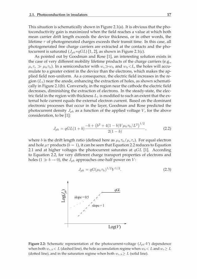
2.1. Photoconduction in insulators 17
This situation is schematically shown in Figure 2.1(a). It is obvious that the pho-toconductivity gain is maximized when the field reaches a value at which bothmean carrier drift length exceeds the device thickness, or in other words, thelifetime τ of photogenerated charges exceeds their transit time. In this case, allphotogenerated free charge carriers are extracted at the contacts and the pho-tocurrent is saturated (Jph=qGL) [1, 2], as shown in Figure 2.1(c).
As pointed out by Goodman and Rose [1], an interesting solution exists inthe case of very different mobility lifetime products of the charge carriers (e.g.,µeτe ≫ µhτh). In a semiconductor with we≫wh and wh<L, the holes will accu-mulate to a greater extent in the device than the electrons, which makes the ap-plied field non-uniform. As a consequence, the electric field increases in the re-gion (L1) near the anode, enhancing the extraction of holes, as shown schemati-cally in Figure 2.1(b). Conversely, in the region near the cathode the electric fielddecreases, diminishing the extraction of electrons. In the steady-state, the elec-tric field in the region with thickness L1 is modified to such an extent that the ex-ternal hole current equals the external electron current. Based on the dominantelectronic processes that occur in the layer, Goodman and Rose predicted thephotocurrent density Jph as a function of the applied voltage V , for the aboveconsideration, to be [1]:
Jph = qGL(1 + b)−b +
(
b2 + 4(1 − b)V µhτh/L2)1/2
2(1 − b), (2.2)
where b is the drift length ratio (defined here as µhτh/µeτe). For equal electronand hole µτ products (b = 1), it can be seen that Equation 2.2 reduces to Equation2.1 and at higher voltages the photocurrent saturates at qGL [1]. Accordingto Equation 2.2, for very different charge transport properties of electrons andholes (1 ≫ b → 0), the Jph approaches one-half power on V :
Jph = qG(µhτh)1/2V 1/2. (2.3)
Figure 2.2: Schematic representation of the photocurrent-voltage (Jph-V ) dependence
when both we,h< L (dashed line), the hole accumulation regime when wh< L and we≥ L
(dotted line), and in the saturation regime when both we,h≥ L (solid line).
18 Chapter 2: Charge transport in polymer:fullerene films
Hence, it is interesting to examine some special or limiting cases of the solutionof Equation 2.2: for equal electron and hole drift lengths (µeτe=µhτh, i.e., b=1),only the linear and saturation regime of Jph(V ) are possible. For very differentcharge transport properties of electrons and holes (e.g. µeτe≫µhτh, i.e., 1 ≫b → 0), the Jph(V ) dependence is dominated by the square-root and saturationregimes. Figure 2.2 shows the Jph(V ) dependence of these two limiting cases.
In the polymer:fullerene blends, charge transfer at the donor/acceptor inter-face produces free electrons and free holes in the two materials. Subsequently,the electrons and holes are extracted at the corresponding electrodes or recom-bine bimolecularly. This last process results in an equal electron and hole life-time, since when an electron disappears also a hole disappears from the device.Hence, in that case an eventual difference in their µτ products mainly originatesfrom a difference in charge carrier mobility. Therefore, determining the chargecarrier mobilities is a crucial step in understanding the photocurrent-voltagecharacteristics of these solar cells.
2.2 Electron transport in fullerene films
2.2.1 Introduction
A promising combination of material for a plastic solar cell is the donor-typeconjugated polymer MDMO-PPV and acceptor-type molecules such as the C60
derivative PCBM [3]. As a concept a bulk heterojunction is used, which consistsof a three dimensional interpenetrating donor-acceptor network, sandwichedbetween two electrodes with different work functions to generate an electricfield across the organic layer. For these kind of cells a power conversion ef-ficiency of 2.5% under AM 1.5 illumination has been reported [4, 5]. Fromphotophysical studies it has been demonstrated that after absorption of a pho-ton, ultra-fast electron transfer takes place from the excited state of a conduct-ing polymer to acceptor molecules such as Buckminster fullerenes (C60), witha quantum efficiency close to unity [6, 7]. Subsequently, the separated chargecarriers are transported via the interpenetrating network to the electrodes. Thephotogenerated current is directly governed by the charge carrier mobility, asis demonstrated in the previous section, alongside the number of photoexcitedcharge carriers.
For the understanding of the opto-electronic properties of MDMO-PPV:PCBMsolar cells, knowledge about the charge transport properties of the individ-ual components is indispensable. For MDMO-PPV the transport of holes hasbeen extensively studied due to its application in polymer light-emitting diodes.From dark current density-voltage (JD-V ) measurements [8], transient electro-luminescent measurements [9], and impedance spectroscopy [10], a hole mobil-ity µh = 5 × 10⁻¹¹ m2/Vs has been obtained for MDMO-PPV at room tempera-ture. The field- (E) and temperature (T ) dependence of the hole mobility in PPVwas described by a stretched exponential dependence
µ(E, T ) = µ0(T ) exp(γ(T )√
E), (2.4)

2.2. Electron transport in fullerene films 19
where µ0(T ) is the zero-field mobility and γ(T ) describes the field activation [8–10]. However, recent developments have shown that, the application of Equa-tion 2.4 to describe the electric field dependence of the charge carrier mobilityin low mobility media is not fully correct due to the fact that the density de-pendence of charge carrier mobility has been neglected [11–13]. Therefore, thevalues of γ at high electric fields are overestimated. In this section, the zero-fieldmobility of electrons in pristine PCBM films is investigated.
2.2.2 Results and Discussion
The devices under investigation consist of a single PCBM layer sandwiched be-tween a hole-conducting layer of PEDOT:PSS, typically of 100 nm thickness, andan evaporated lithium fluoride (LiF; ≈1 nm)/ aluminum (Al; ≈100 nm) top elec-trode (see Section 2.4). In the inset of Figure 2.3, an energy band diagram of thedevice is shown under flat-band condition.
From the work functions, it is expected that LiF/Al forms an Ohmic con-tact for electron injection into PCBM. The work function of PEDOT:PSS (5.2 eV)does not match the HOMO level of PCBM (6.1 eV) [3], thus hole injection fromPEDOT:PSS into PCBM can be neglected. Consequently, only electrons are ex-pected to flow through PCBM under forward bias conditions. Furthermore,from the energy band diagram at room temperature a built-in voltage VBI ofaround 1.5 V is expected. The JD-V measurements are performed in nitrogenatmosphere within a temperature range of 150-300 K. With deceasing tempera-ture VBI is expected to typically increase by 0.3 V in the range 300-150 K, dueto diffusion of thermally injected charges [14]. The active area amounts to 10−5
m2. In Figure 2.3, the experimental JD-V characteristics at room temperature(295 K) are shown for PCBM devices with layer thicknesses, L, of 90 nm and 170
Figure 2.3: Experimental (symbols) and calculated (solid lines) JD-V characteristics of
ITO/PEDOT:PSS/PCBM/LiF/Al devices with thicknesses L=90 nm and 170 nm, using
VBI=1.4 V and RS=30 Ω. The device band diagram is indicated in the inset. The electron
transport is described by SCLC (Equation 2.5) with an electron mobility µe = 2.0 × 10⁻⁷
m2/Vs and a dielectric constant ǫr=3.9.

20 Chapter 2: Charge transport in polymer:fullerene films
0.0 0.5 1.0 1.5 2.0 2.5 3.0 3.510-2
10-1
100
101
102
103
104 L=170 nm
295 K250 K210 K170 K
J D [A
/m2 ]
V-VRS-VBI [V]
Figure 2.4: Experimental JD-V characteristics of an ITO/PEDOT:PSS/PCBM/LiF/Al
device with thickness L=170 nm for various temperatures (symbols). The solid lines
represent the calculated JD-V characteristics as predicted by a SCLC model using the
field-dependent mobility defined by Equation 2.4.
nm.
Using VBI=1.4 V it is observed from the slope of the log(JD) versus log(V )plot that the current density JD depends quadratically on voltage. This behavioris characteristic for a space-charge limited current (SCLC) given by [15]
JD =9
8ǫ0ǫrµe
V 2
L3, (2.5)
where ǫ0ǫr is the permittivity of PCBM. From capacitance-voltage measure-ments we have obtained a relative dielectric constant ǫr of 3.9 for PCBM. Usingǫr=3.9, we find that the JD-V characteristics of our devices with L=90 and 170nm are well described by Equation 2.5, with µe = 2.0 × 10⁻⁷ m2/Vs. Thus,the observation of SCLC provides direct information on the electron mobility inPCBM. It should be noted that for current densities larger than 1000 A/m2, theapplied voltage should be corrected for the voltage drop across the ITO seriesresistance (VRS), which typically amounts to 25-30 Ω in our substrates. An im-portant conclusion is that, at room temperature, the electron mobility of PCBMis a factor of 4000 larger than the hole mobility of pristine MDMO-PPV [8–10].The observed electron mobility of 2.0 × 10⁻⁷ m2/Vs in PCBM is a factor of 40less than mobilities reported from field-effect measurements on thin films ofevaporated C60, which are typically 8×10⁻⁶ m2/Vs [16]. For C60 single-crystalsgrown from the vapor phase, mobilities of 5× 10⁻⁵ m2/Vs have been measuredby time-of-flight experiments [17]. The reduction of the mobility in PCBM filmsas compared to C60 single crystals indicates that disorder may play an importantrole in PCBM thin films.
Figure 2.4 shows the JD-V characteristics of a PCBM device with L=170 nmas a function of temperature. In order to describe the electron current in PCBM,the SCLC model is combined with the field-dependent mobility of Equation 2.4.
2.2. Electron transport in fullerene films 21
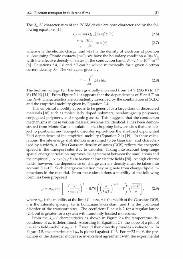
The JD-V characteristics of the PCBM device are now characterized by the fol-lowing equations [15]
JD = qn(x)µe[E(x)]E(x) (2.6)
ǫ0ǫr
q
dE(x)
dx= n(x), (2.7)
where q is the electric charge, and n(x) is the density of electrons at positionx. Assuming Ohmic contacts (x=0), we have the boundary condition n(0)=Nc,with the effective density of states in the conduction band, Nc=2.5 × 1025 m−3
[8]. Equations 2.4, 2.6 and 2.7 can be solved numerically for a given electroncurrent density JD. The voltage is given by
V =
∫ L
0
E(x)dx (2.8)
The built-in voltage VBI has been gradually increased from 1.4 V (295 K) to 1.7V (150 K) [14]. From Figure 2.4 it appears that the dependencies of E and T onthe JD-V characteristics are consistently described by the combination of SCLCand the empirical mobility given by Equation 2.4.
This empirical mobility appears to be generic for a large class of disorderedmaterials [18] such as molecularly doped polymers, pendant-group polymers,conjugated polymers, and organic glasses. This suggests that the conductionmechanisms in these various material systems are identical. It has been demon-strated from Monte-Carlo simulations that hopping between sites that are sub-ject to positional and energetic disorder reproduces the stretched exponentialfield dependence of the empirical mobility (Equation 2.4) [19]. In these calcu-lations, the site energy distribution is assumed to be Gaussian, and character-ized by a width, σ. This Gaussian density of states (DOS) reflects the energeticspread in the transport sites due to disorder. Taking into account long-rangespatial energy correlation improves the agreement between the simulations and
the empirical µ ∝ exp(γ√
E) behavior at low electric fields [20]. At high electricfields, however, the dependence on charge carriers density must be taken intoaccount [11–13]. Such energy-correlation may originate from charge-dipole in-teractions in the material. From these simulations a mobility of the followingform has been proposed
µ = µ∞ exp
[
−(
3σ
5kBT
)2
+ 0.78
(
(
σ
kBT
)3/2
− Γ
)
√
qaE
σ
]
, (2.9)
where µ∞ is the mobility at the limit T → ∞, σ is the width of the Gaussian DOS,a is the intersite spacing, kB is Boltzmann’s constant, and Γ is the positionaldisorder of the transport sites. The coefficient Γ equals 2 for a regular lattice[20], but is greater for a system with randomly located molecules.
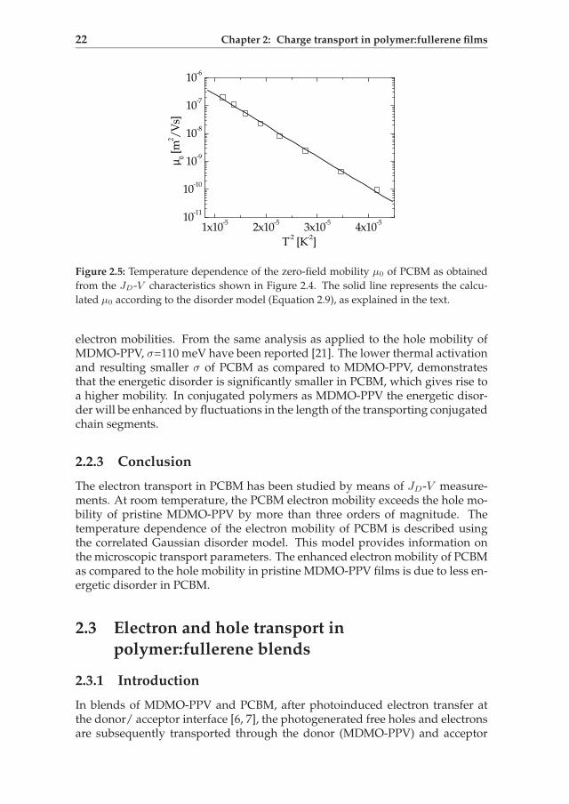
From the JD-V characteristics as shown in Figure 2.4 the temperature de-pendence of µ0 is determined. According to Equation 2.9, the slope of a plot ofthe zero field-mobility µ0 ∝ T−2 would then directly provides a value for σ. InFigure 2.5, the experimental µ0 is plotted against T−2. For σ=73 meV, the pre-diction of the disorder model are in excellent agreement with the experimental
22 Chapter 2: Charge transport in polymer:fullerene films
1x10⁻⁵
2x10⁻⁵
3x10⁻⁵
4x10⁻⁵
10-11
10-10
10-9
10-8
10-7
10-6
µ 0 [m
2 /V
s]
T-2 [K
-2]
Figure 2.5: Temperature dependence of the zero-field mobility µ0 of PCBM as obtained
from the JD-V characteristics shown in Figure 2.4. The solid line represents the calcu-
lated µ0 according to the disorder model (Equation 2.9), as explained in the text.
electron mobilities. From the same analysis as applied to the hole mobility ofMDMO-PPV, σ=110 meV have been reported [21]. The lower thermal activationand resulting smaller σ of PCBM as compared to MDMO-PPV, demonstratesthat the energetic disorder is significantly smaller in PCBM, which gives rise toa higher mobility. In conjugated polymers as MDMO-PPV the energetic disor-der will be enhanced by fluctuations in the length of the transporting conjugatedchain segments.
2.2.3 Conclusion
The electron transport in PCBM has been studied by means of JD-V measure-ments. At room temperature, the PCBM electron mobility exceeds the hole mo-bility of pristine MDMO-PPV by more than three orders of magnitude. Thetemperature dependence of the electron mobility of PCBM is described usingthe correlated Gaussian disorder model. This model provides information onthe microscopic transport parameters. The enhanced electron mobility of PCBMas compared to the hole mobility in pristine MDMO-PPV films is due to less en-ergetic disorder in PCBM.
2.3 Electron and hole transport in
polymer:fullerene blends
2.3.1 Introduction
In blends of MDMO-PPV and PCBM, after photoinduced electron transfer atthe donor/ acceptor interface [6, 7], the photogenerated free holes and electronsare subsequently transported through the donor (MDMO-PPV) and acceptor

2.3. Electron and hole transport in polymer:fullerene blends 23
(PCBM) phases to the anode and cathode, respectively, resulting in an exter-nal photocurrent density Jph. Since the photocurrent is not solely governed bythe generation rate G of free electron-hole pairs, but also by recombination pro-cesses, the charge-transport properties of the semiconductor are determinativefor an efficient photoresponse. As shown in Section 2.1, the recombination of thefree charge carriers is significant, if the mean carrier drift length w of one or bothcharge-carrier species is smaller than the device thickness L. In other words,recombination is important as long as the transit time of the photogeneratedcharge carriers is longer than their lifetime. However, if both mean carrier driftlengths exceed the thickness of the film (L), no recombination occurs and theelectrodes extract all photogenerated charge carriers. In this saturation regime,both electron and hole lifetimes equal the transit times of the charge carriers andthe photocurrent density is saturated (Jsat
ph = qGL) [1, 2, 22].Since the hole mobility of pristine MDMO-PPV has previously been reported
to be 5×10⁻¹¹ m2/Vs [8–10], whereas an electron mobility for PCBM of 2×10⁻⁷
m2/Vs has been determined in Section 2.2, the charge transport in heterojunc-tion photovoltaic cell based on these materials is expected to be strongly unbal-anced (µe≫µh). This has deep impact on the photoresponse of the respectivecell, as demonstrated in Section 2.1. Due to the unbalanced charge-transportproperties, holes accumulate to greater extent in the device than electrons do,as shown in Figure 2.1(b). Under steady-state conditions, the electric field inregion with thickness L1 is modified to such an extent that the external holecurrent equals the external electron current. However, in the region L1, elec-trons do not neutralize the accumulated holes, which results in build-up of pos-itive space-charge. The electrostatic limit of hole accumulation is reached whenthe photogenerated current density Jph1 = qGL1 is equal to the space-charge-limited current density in region L1 [1]:
Jph1 = qGL1 ≤ JSCLC1 =9
8ǫ0ǫrµh
V 21
L31
, (2.10)
where JSCLC1 is the space-charge-limited current density across the region ofstrong hole accumulation, V1 is the voltage drop over this region, and ǫ0ǫr is thedielectric permittivity. Since almost the entire voltage V drops in the region ofhole accumulation (V1 ≈ V ), the maximal electrostatically allowed photocurrentdensity Jmax
ph is given by [1]:
Jph ≤ Jmaxph = (qG)0.75
(
9
8ǫ0ǫrµh
)0.25 √V (2.11)
Note that Jmaxph scales with the square-root of the voltage and depends on the
charge carrier mobility of the slowest charge carrier species as well as the gener-ation rate of free electron-hole pairs. A more detailed analysis of this is given inSection 3.2 of this thesis. In order to be able to predict the electrostatic limit, in-formation on G is still required. The magnitude of G can be estimated from thephotocurrent density at the transition to the saturation regime [1]. For a typicalphotovoltaic cell based on MDMO-PPV and PCBM, 2 × 1027 free electron-holepairs are generated per second and cubic meter, upon illumination with 800W/m2 from a halogen lamp.
24 Chapter 2: Charge transport in polymer:fullerene films
0.01 0.1 1
1
10
J ph [
A/
m2 ]
VOC
-V [V]
T= 295 KL=95 nm
Figure 2.6: Photocurrent-voltage dependence of an ITO/PEDOT:PSS/MDMO-
PPV:PCBM/LiF/Al photovoltaic cell (circles). The dotted line indicates the satu-
ration current. The dashed line is the space-charge-limited photocurrent calculated
using the µh of pristine MDMO-PPV and generation rate of free electron-hole pairs of
2×1027 m−3s−1. The continuous line is the space-charge-limited photocurrent calculated
by assuming µh=10−8 m2/Vs.
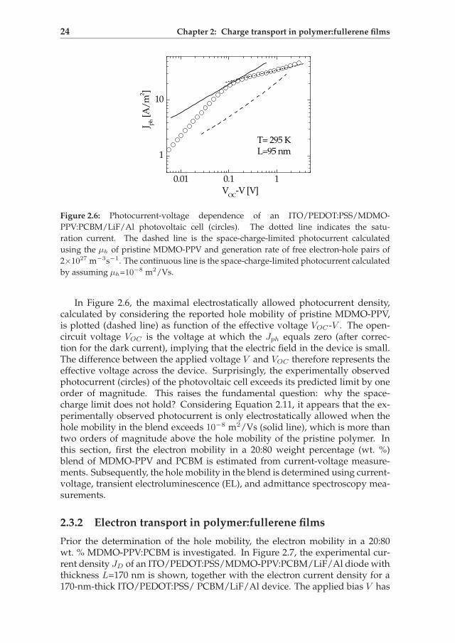
In Figure 2.6, the maximal electrostatically allowed photocurrent density,calculated by considering the reported hole mobility of pristine MDMO-PPV,is plotted (dashed line) as function of the effective voltage VOC-V . The open-circuit voltage VOC is the voltage at which the Jph equals zero (after correc-tion for the dark current), implying that the electric field in the device is small.The difference between the applied voltage V and VOC therefore represents theeffective voltage across the device. Surprisingly, the experimentally observedphotocurrent (circles) of the photovoltaic cell exceeds its predicted limit by oneorder of magnitude. This raises the fundamental question: why the space-charge limit does not hold? Considering Equation 2.11, it appears that the ex-perimentally observed photocurrent is only electrostatically allowed when thehole mobility in the blend exceeds 10−8 m2/Vs (solid line), which is more thantwo orders of magnitude above the hole mobility of the pristine polymer. Inthis section, first the electron mobility in a 20:80 weight percentage (wt. %)blend of MDMO-PPV and PCBM is estimated from current-voltage measure-ments. Subsequently, the hole mobility in the blend is determined using current-voltage, transient electroluminescence (EL), and admittance spectroscopy mea-surements.
2.3.2 Electron transport in polymer:fullerene films
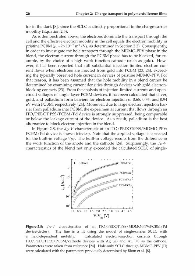
Prior the determination of the hole mobility, the electron mobility in a 20:80wt. % MDMO-PPV:PCBM is investigated. In Figure 2.7, the experimental cur-rent density JD of an ITO/PEDOT:PSS/MDMO-PPV:PCBM/LiF/Al diode withthickness L=170 nm is shown, together with the electron current density for a170-nm-thick ITO/PEDOT:PSS/ PCBM/LiF/Al device. The applied bias V has

2.3. Electron and hole transport in polymer:fullerene blends 25
0.0 0.5 1.0 1.5 2.0 2.510
-1
100
101
102
103
104
0.1 110
-1
101
103
J D [
A/
m2 ]
V-VBI
-VRS
[V]
T=290 KL=170 nm
J D [
A/
m2 ]
V-VBI
-VRS
[V]
Figure 2.7: Experimental JD-V characteristics of an ITO/PEDOT:PSS/MDMO-
PPV:PCBM (20:80 wt. %)/LiF/Al diode in the dark (squares), together with a PCBM
electron only device (triangles) with a thickness of L=170 nm, at a temperature T=290 K.
The JD-V characteristics are corrected for voltage drop across the ITO serial resistance
VRS (RS≈11 Ω) and for a built-in voltage (VBI=1.4 V) that arises from the work function
difference between the contacts. The inset shows the same data in a log-log plot to
demonstrate that the current density depends quadratically on the voltage, characteristic
for SCLC.
been corrected for the built-in voltage (VBI=1.4 V) that arises from the workfunction difference between the ITO/PEDOT:PSS and LiF/Al contacts. For largecurrent densities (larger than 1000 A/m2), the applied voltage has also beencorrected for the voltage drop across the ITO series resistance (VRS), which istypically 11 Ω in these experiments. The slope of the log(JD)-log(V ) plot (insetof Figure 2.7) demonstrates that the current density depends quadratically onthe voltage (JD ∝ V 2), consistent with SCLC. It appears from Figure 2.7 that inforward bias the dark current in MDMO-PPV:PCBM (20:80 wt. %) bulk hetero-junction diodes is equal to the electron current in pristine PCBM. The fact thatthe experimental JD-V curve of the bulk heterojunction diode lies on top of thePCBM device indicates that dark current of the blend is governed by electronsand the electron mobility of PCBM in the bulk heterojunction is not significantlyaffected by the presence of MDMO-PPV up to 20 wt. %. Furthermore, the SCLCbehavior of PCBM demonstrates that the use of LiF/Al does not represent a sig-nificant barrier for electron injection. In order to investigate the hole current in aMDMO-PPV:PCBM bulk heterojunction diode, the electron current needs to bestrongly suppressed. In the following, this type of devices are used to measurethe transport of holes in the MDMO-PPV phase of the blend.
2.3.3 Hole transport in polymer:fullerene films
Current-voltage measurements
A frequently used tool for investigating charge-carrier mobilities of low mobilitymedia is to examine the space-charge-limited current through the semiconduc-
26 Chapter 2: Charge transport in polymer:fullerene films
tor in the dark [8], since the SCLC is directly proportional to the charge-carriermobility (Equation 2.5).
As is demonstrated above, the electrons dominate the transport through thecell and the effective electron mobility in the cell equals the electron mobility inpristine PCBM (µe=2×10⁻⁷ m2/Vs; as determined in Section 2.2). Consequently,in order to investigate the hole transport through the MDMO-PPV phase in theblend, the electron current through the PCBM phase has to be blocked, for ex-ample, by the choice of a high work function cathode (such as gold). How-ever, it has been reported that still substantial injection-limited electron cur-rent flows when electrons are injected from gold into PCBM [23, 24], exceed-ing the typically observed hole current in devices of pristine MDMO-PPV. Forthat reason, it has been assumed that the hole mobility in a blend cannot bedetermined by examining current densities through devices with gold electron-blocking contacts [23]. From the analysis of injection-limited currents and open-circuit voltages of single-layer PCBM devices, it has been calculated that silver,gold, and palladium form barriers for electron injection of 0.65, 0.76, and 0.94eV with PCBM, respectively [24]. Moreover, due to large electron injection bar-rier from palladium into PCBM, the experimental current that flows through anITO/PEDOT:PSS/PCBM/Pd device is strongly suppressed, being comparableor below the leakage current of the device. As a result, palladium is the bestalternative to block electron injection in the blend.
In Figure 2.8, the JD-V characteristic of an ITO/PEDOT:PSS/MDMO-PPV:PCBM/Pd device is shown (circles). Note that the applied voltage is correctedfor the built-in voltage VBI . The built-in voltage results from the difference inthe work function of the anode and the cathode [24]. Surprisingly, the JD-Vcharacteristics of the blend not only exceeded the calculated SCLC of single-
0.0 0.5 1.0 1.5 2.0 2.5 3.0 3.5 4.0 4.5
10-2
10-1
100
101
102
L = 310 nm
MDMO/Au
PCBM/Au
PCBM/Ag
blend/Pd
J D [A
/m2 ]
V-VBI [V]
Figure 2.8: JD-V characteristics of an ITO/PEDOT:PSS/MDMO-PPV:PCBM/Pd
device(circles). The line is a fit using the model of single-carrier SCLC with
a field-dependent mobility. Calculated electron-injection currents through
ITO/PEDOT:PSS/PCBM/cathode devices with Ag () and Au () as the cathode.
Parameters were taken from reference [24]. Hole-only SCLC through MDMO-PPV ()
were calculated with the parameters previously determined by Blom et al. [8].

2.3. Electron and hole transport in polymer:fullerene blends 27
10-3 10-2 10-1 10010-8
10-7
10-6
10-5
10-4
J D×L
[A/m
]
E2 [1014 (V/m)2]
(a)
Figure 2.9: (a) JD-V characteristics of an ITO/PEDOT:PSS/MDMO-PPV:PCBM/Pd ()
and an ITO/PEDOT:PSS/MDMO-PPV:PCBM/Ag (©) device. The line is a fit using the
model of single-carrier SCLC with a field-dependent mobility. (b) The energy band dia-
grams of a solar cell with various cathode metals [24].
layer MDMO-PPV hole-only device (), but also exceeded the calculated elec-tron injection-limited currents from silver () and gold () into PCBM, whichare both better electron injectors than palladium. There are two possible expla-nations for this strongly enhanced current in the blend. First, the observed cur-rent is a hole-only current, meaning that the hole mobility is strongly enhancedcompared to that of pristine MDMO-PPV. Secondly, the observed current is anelectron current and the injection-limited electron current from palladium intoPCBM is strongly enhanced by the presence of holes, and was therefore notcomparable to the injection-limited electron current observed with single-layerPCBM devices.
Whether or not the observed current densities in the blend were influencedby electron injection from the cathode into PCBM was verified by changing thecathode metal, thereby altering the charge-injection barriers. In Figure 2.9(a), itis shown that the current through a device based on a blend remains unchanged,even when the cathode is changed from palladium to silver. A schematic banddiagram is shown in the Figure 2.9(b). Consequently, any contribution of elec-trons to the current is highly unlikely, and, in the analysis of the JD-V charac-teristics, we regard the device as a hole-only device.
The current densities obtained from an ITO/PEDOT:PSS/MDMO-PPV:PCBM/Pd device scale quadratically with the applied voltage [Figure 2.9(a)], which isindicative of space-charge limited transport. Assuming that the device is hole-dominated, the JD-V measurements thus provide information on the hole mo-bility of the MDMO-PPV phase in the blend. Similar to the findings in pristineMDMO-PPV [8] and PCBM (Section 2.2), the hole mobility was field-dependentin a stretched exponential form, as given by the Equation 2.4. By simulating theSCLC of the hole-only devices of Figure 2.9(a), a zero-field mobility for holes inMDMO-PPV phase of the blend of µh = 1.5×10⁻⁸ m2/Vs and a field activationfactor γh = 1.4 × 10⁻⁴ m1/2/V1/2 were obtained at room temperature.

28 Chapter 2: Charge transport in polymer:fullerene films
1k 100k 10M1
2
3
4
(b)
0V
2V3V4V
1V
C [n
F]
Frequency [Hz]
(a)
1k 10k 100k 1M
0.8
0.9
1.0
1.1
1.2
C/C
0V
Figure 2.10: (a) Capacitance-frequency plot of an ITO/PEDOT:PSS/MDMO-PPV:PCBM
/Pd device at different DC bias. The respective capacitance traces are offset for clarity.
The layer thickness was 310 nm. (b) Capacitance normalized to zero DC bias capacitance
versus frequency for 3 V (), 3.5 V (©), and 4 V () DC bias. The lines are fits with the
admittance model for space-charge limited conduction given by Martens et al. [10].
Admittance spectroscopy
A powerful technique for investigating charge transport in conjugated polymersis admittance spectroscopy. This technique has already been used for determin-ing transit times (τt) and, hence, charge carrier mobilities of pristine MDMO-PPV [10]. In a diode, where direct currents (DC) are space-charge limited, asmall alternating current (AC) disturbance of the DC bias changes the space-charge density in the semiconductor, if the frequency ω is below τ−1
t . The space-charge build-up is delayed with respect to the AC stimulus, resulting in an in-ductive contribution to the capacitance. For frequencies ω > τ−1
t , the additionalspace-charge build-up can not fallow the AC stimulus and the geometric ca-pacitance is measured. Consequently, τt of the charge carriers is given by thethreshold frequency, below which a reduction in capacitance is observed. Anadvantage of this technique is that for devices where both electrons and holesare present, such as in the case of MDMO-PPV-based light-emitting diodes, therespective transport properties can be individually monitored, since they areseparated in frequency space [25].
In Figure 2.10, it is shown by admittance measurements that ITO/PEDOT:PSS/MDMO-PPV:PCBM/Pd devices exhibit a capacitance decrease below a certainthreshold frequency. The fact that an inductive contribution to the capacitancewas present confirms that the DC currents through these devices were space-charge limited. For a strongly injection-limited device the amount of injectedcharge is too small to exhibit an inductive contribution to the capacitance. Theobserved threshold frequency shows a clear trend upon changes in DC bias.By increasing the DC bias, the threshold frequency was shifted to higher fre-quencies, reflecting a reduction of the transit time of the charge carriers. Fromthe frequency response of the capacitance, the transit times were determined

2.3. Electron and hole transport in polymer:fullerene blends 29
by simulating the capacitance frequency dependence with a model for space-charge limited admittance [10]. The resulting hole mobilities in the MDMO-PPVphase of the blend for different DC fields are depicted in Figure 2.12. They arein excellent agreement with the mobilities obtained by simulating the DC SCLC(Figure 2.9). Since the mobility of the electrons in the blend can be estimated[23], the threshold frequency for electron transport can be predicted, and is typ-ically one order of magnitude above the observed threshold frequencies. Theabsence of any inductive contribution at these higher frequencies is indicativeof a hole-dominated device.
Transient Electroluminescence
As a final proof that the transport in the investigated devices was dominantedby holes, and that it is conceivable that the SCLC and admittance spectroscopyunveiled the hole mobility in the MDMO-PPV phase, a modified transient elec-troluminescence (EL) technique was applied. Transient EL has frequently beenused to estimate charge-carrier mobilities in highly luminescent organic thinfilms [9, 26–28]. Upon applying a rectangular voltage pulse to a diode, holes andelectrons are injected at the corresponding electrodes and traverse the lumines-cent organic semiconductor until they meet and radiative recombination occurs.A time delay between the onset of the applied voltage and the appearance of theEL is directly related to the transit times of the charge carriers. Advantage can betaken of the fact that hole mobilities in PPV-type materials typically exceed theelectron mobilities [27, 29, 30]. The delay between voltage onset and the appear-ance of the EL is, therefore, primarily related to the τt of the faster charge-carrierspecies.
As desired in photovoltaic cells, the luminescence in a blend of MDMO-PPVand PCBM is strongly quenched, which complicates the determination of thetransit times with EL transient measurements. However, by introducing a lumi-nescent layer between the blend and the cathode, this difficulty can be circum-vented. In such double-layer diodes, holes are injected from the anode into theMDMO-PPV phase of the blend and electrons are injected from the cathode intothe luminescent layer, as shown schematically in the inset of Figure 2.11. Sinceradiative recombination exclusively occurs in the luminescent layer, holes haveto traverse the entire blend in order to participate in the recombination. Assum-ing a low electron mobility in the luminescent layer, the time delay between theEL signal and the stimulus (τ total
t ) is given by the transit times of holes passingthe blend (τ blend
t ) and the luminescent layer (τ lumt ):
τ totalt = τ blend
t + τ lumt (2.12)
The PPV-based oligomer (E,E,E,E)-1,4-bis[(4-styryl)styryl]-2-methoxy-5-(2’ -ethylhexyloxy)benzene (MEH-OPV5) was used as the luminescent layer, sinceits highest occupied molecular orbital (HOMO) matches that of MDMO-PPVand its electron mobility is known to be below its hole mobility [28, 31]. Fur-thermore, because MEH-OPV5 can be deposited by thermal vacuum deposition,intermixing of the blend and the MEH-OPV5 cover layer is prevented. A high

30 Chapter 2: Charge transport in polymer:fullerene films
Figure 2.11: Transit times of holes from EL transient measurements for
ITO/PEDOT:PSS/ MEH-OPV5/Ba devices with 100 nm (©) and 160 nm () layer
thickness and an ITO/PEDOT:PSS /MDMO-PPV:PCBM/MEH-OPV5/Ba device with
200 nm layer thickness of the blend and 60 nm layer thickness (LMEH ) of MEH-OPV5
(•). The dashed line is a fit using τt ∝ (L/E)1/α. The dotted line indicates the transit
times of double-layer diodes with transport dispersion in the MEH-OPV5 layer, but no
dispersion in the blend and a constant hole mobility. The continuous line is a fit using
Equations 2.12 and 2.13 with field-dependent mobility given by the Equation 2.4. The
inset schematically shows the operation principle of the EL transient technique in the
double-layer configuration.
EL brightness at low bias was guaranteed by using PEDOT:PSS as the anodeand barium as the cathode.
In order to investigate the transit times of charge carriers passing the blend ina double-layer arrangement, the transit times through the MEH-OPV5 film werefirst investigated. In Figure 2.11, the transit times for single-layer MEH-OPV5devices are shown for film thicknesses of 100 and 160 nm (empty symbols). Therevealed transit times are in agreement with those previously reported [28]. Thefield and thickness dependence of the transit times could be described by τt ∝(L/E)1/α with α ≈ 0.88, indicating weak dispersivity of the hole transport inMEH-OPV5 [32].
The EL spectrum obtained from a double-layer diode of the blend and MEH-OPV5 was equal to the emission spectrum of a pure MEH-OPV5 layer, con-firming that holes did indeed travel through the entire blend. For a double-layer diode with a total thickness of 260 nm, the measured transit times (Figure2.11, solid symbols) were, however, only slightly longer than those found forthe single-component MEH-OPV5 film. This suggests that the transit times ofcharge carriers passing the blend were even shorter than those of charge carriers

2.3. Electron and hole transport in polymer:fullerene blends 31
1 2 3 4 5 610-10
10-9
10-8
10-7
h (MDMO)
e (PCBM)
h (MDMO
MDMO:PCBM)
[m2 /V
s]
E1/2 [103 (V/m)1/2]
Figure 2.12: Charge carrier mobilities versus the square-root of the electric field. The
hole mobility of pristine MDMO-PPV was taken from Blom et al. [8] and the electron
mobility of pristine PCBM was determined in Section 2.2 of this thesis. The hole mo-
bilities of the MDMO-PPV phase in the blend with PCBM were obtained by examining
the SCLC of hole-only devices (), by admittance spectroscopy (⋄), and by EL transient
measurements for 200 nm () and 120 nm (©) layer thickness of the blend and 60 nm
MEH-OPV5.
passing the MEH-OPV5 layer. If we convert the observed transit times for theblend directly into a mobility using Equation 2.13,
µh =Lblend
τ blendt E
, (2.13)
it appears from Figure 2.12 ( and ©) that the obtained hole mobilities are closeto those found with both DC JD-V measurements and admittance spectroscopy.This indicates that the hole transport through the blend is not (or only slightly)dispersive. The accordance between mobilities obtained from transient EL mea-surements and mobility unveiled by JD-V and admittance measurements isconclusive proof that the charge transport in ITO/PEDOT:PSS/MDMO-PPV:PCBM/Pd devices is hole-dominated and enhanced.
Discussion
A remarkable agreement between the hole mobilities obtained from DC JD-Vmeasurements, admittance spectroscopy, and transient EL measurements hasbeen observed (Figure 2.12). Accordingly, the room temperature hole mobilityin the blend of MDMO-PPV and PCBM is 2×10⁻⁸ m2/Vs for an electric fieldof 4×10⁶ V/m, which is only one order of magnitude lower than the respectiveelectron mobility in pristine PCBM and 200-fold higher than the hole mobilityin the pristine polymer. A changed hole mobility in donor-like polymers uponblending with PCBM has already been reported [33, 34]. The charge carrier mo-bilities in the blend of MDMO-PPV and PCBM were measured, for instance,

32 Chapter 2: Charge transport in polymer:fullerene films
by Choulis et al., using time-of-flight photocurrent measurements [34]. Theyreported that the hole mobility in the MDMO-PPV phase of a blend decreasesupon adding PCBM below its percolation threshold from 2.4×10⁻¹⁰ m2/Vs to2.3×10−11 m2/Vs at 2.2×10⁷ V/m and increase again above the percolationthreshold of PCBM to approximately 2×10⁻¹⁰ m2/Vs for a blend of 20:80 wt. %of MDMO-PPV:PCBM. Nonetheless, the hole mobility was found to be far be-low the measured electron mobility in PCBM (see Section 2.2). Hence, it wasbelieved that space-charge effects restrain the photoresponse of a photovoltaiccell, which is, however, in contradiction to the observed photocurrents (Figure2.6). Since, for example, a photocurrent governed by square-root dependenceon V (Equation 2.11) does not allow fill factors larger than ≈40%, the typicallyobserved fill factors of 60% [4] are inaccessible in the space-charge limit. Yet, thehole mobility reported herein is consistent with the reported photoresponse ofa cell, exceeding the minimum hole mobility of 10−8 m2/Vs, which is requiredfor the electrostatically allowed photocurrent. Space-charge effects and the con-comitant charge carrier recombination, hence, do not limit the photoresponse,and fill factors of 60% are conceivable. The discrepancy between the hole mobil-ities reported here and those of Choulis et al. might be related to differences inthe film morphology arising from differences in the sample preparation, whichare essential for obtaining the desire device. Whereas a layer of 1 µm was re-quired for transient photocurrent measurements, the devices we investigatedexhibited a layer thickness equal to or smaller than 300 nm, coming closer to thedevice thickness that is usually used in the photovoltaic cells.
Why the hole mobility in the MDMO-PPV increases upon blending the poly-mer with an excess of PCBM remains an unsolved question. Recently, it has beendemonstrated that the charge carrier mobility in MDMO-PPV as extracted fromhole-only diodes and field-effect transistors can differ by more than three ordersof magnitude [12]. This large difference originates from the strong dependenceof the mobility on charge carrier density. However, in the space-charge limiteddevice investigated herein, the carrier densities are low and this effect can notbe responsible for the observed mobility increase upon blending with PCBM.Pacios et al. proposed that a change in film morphology upon increased PCBMconcentration results in an enhanced intermolecular interaction and, hence, in
Figure 2.13: (a) The molecular conformation of pristine MDMO-PPV according to Ke-
merink et al. [35]. (b) Upon mixing MDMO-PPV with PCBM interactions between the
two moieties might change the molecular conformation of MDMO-PPV.

2.3. Electron and hole transport in polymer:fullerene blends 33
Figure 2.14: Hole mobility (µh) of a symmetrical substituted PPV (BEH1BMB3-PPV) as
a function of weight percentage PCBM in the PPV:PCBM blend films. The inset shows
the chemical structures of symmetrical substituted PPV (upper image) and PCBM (lower
image).
an improved charge transfer between adjacent molecules [33]. Recent obser-vation on the molecular level concerning the film morphology of MDMO-PPVsuggest a similar scenario. It was found that films of MDMO-PPV exhibit inter-connected ring-like features, which were attributed to ring-like bent chains, asschematically depicted in Figure 2.13(a) [35].
The molecular conformation was understood in terms of interactions be-tween adjacent aliphatic side chains on one single chain. Due to the asymmet-ric side-chain substituents in MDMO-PPV, the interaction causes a bending ofthe otherwise rigid polymer backbone. Hence, a conformation of the polymer,where the substituents of the same species preferably point to one side of thebackbone, results in a circular bending of the chain. It has been shown that ring-like, bent polymer chains randomly stack in a pronounced two-dimensionalmanner. The relevant molecular conformation and the weakly ordered stack-ing of the molecules might be the origin of the poor transport properties of thepristine MDMO-PPV, since they are likely to result in a high disorder energyand in poor π-π interaction. However, upon blending MDMO-PPV with PCBM,the situation might change, that is, when the formation of the ring-like molec-ular conformation is hindered due to interactions between MDMO-PPV andPCBM [Figure 2.13(b)]. On the basis of this assumption, an improvement in thecharge transport properties can be expected, resulting from a reduced nearest-neighbor hopping distance and/or a lower disorder energy. From temperature-dependent measurements, a change in the disorder energy of 0.01 eV could beestimated. Whether this explanation can predict an increase in the hole mo-bility of more than two orders of magnitude, however, is not clear at present.Modifying the hole-transport properties by systematically changing the chem-ical structure of the donor-like polymers as well as the PCBM concentration inthe blend might give an answer to this question.
The morphology studies also revealed that the chains of a symmetricallysubstituted polymer show a linear orientation in the film [35]. Therefore, we

34 Chapter 2: Charge transport in polymer:fullerene films
have further investigated the hole mobility in a symmetrical substituted PPVand PCBM blends. The PPV used in this investigation is a random co-polymerpoly[2,5-bis(2‘-ethylhexyloxy)-co-2,5-bis(2‘-methylbutyloxy)-1,4-phenylene viny-lene] (BEH1BMB3-PPV), with its chemical structure shown in the inset of Figure2.14. For this symmetrically substituted PPV, when blended with PCBM at dif-ferent weight percentages, we observe that the hole mobility in the PPV phaseis hardly affected compared with that measured in pristine PPV, as shown inFigure 2.14. This indicates that the molecular conformation of the MDMO-PPVin the presence of PCBM is the reason for the enhanced hole mobility measuredin these blends.
2.3.4 Conclusion
In this section, the electron and hole mobility in 20:80 weight percentage blendsof MDMO-PPV:PCBM is determined. It is shown that the electrons dominate thetransport through the cell and that the effective charge-carrier mobility in thecell equals the electron mobility in pristine PCBM (µe=2×10⁻⁷ m2/Vs). Withrespect to hole mobility, we have presented consistent experimental evidencethat, upon blending MDMO-PPV with PCBM, the hole mobility in the MDMO-PPV phase is enhanced by more than two orders of magnitude, compared tothe pristine polymer. A hole mobility of around 2×10⁻⁸ m2/Vs was disclosed,which is only one order of magnitude lower than the electron mobility in PCBM.Consequently, the charge transport in a bulk heterojunction solar cell based onMDMO-PPV and PCBM is much more balanced than earlier believed and space-charge build-up is therefore not limiting the photoresponse. These results shinenew light on the high external quantum efficiencies observed in these photo-voltaic cells.
2.4 Experimental section
Device Preparation: Prepatterned ITO-coated glass substrates were wet-cleanedby rubbing with soap, rinsing with water, and ultrasonic cleaning in acetoneand 2-propanol. The substrates were further UV-ozone treated and a layer ofPEDOT:PSS (Bayer AG) was subsequently spin-coated on the pre-cleaned ITO,using a Convac spin-coater. The PEDOT:PSS layer was dried at an elevatedtemperature. The samples were then inserted into a glove box filled with ni-trogen. A thin layer of a blend of MDMO-PPV:PCBM in a 20:80 wt. % wasthen spin-coated from a chlorobenzene solution (with a concentration of ≈3.3to 6 mg PPV/mL) using a Karl Suss spin-coater. The pristine PCBM samplesused to investigate electron mobility in Section 2.2 were spin-coated in air, atroom temperature, from a chlorobenzene solution with a concentration of about30 mg/mL. For transient EL measurements, a thin MEH-OPV5 layer was sub-sequently vacuum-deposited at 10−6 mbar on the blend. Finally, top contactswere deposited via vacuum deposition at 10−7 mbar.Device Characterization: All measurements were performed under a nitro-gen atmosphere. J-V measurements were performed with a Keithley 2400

2.4. Experimental section 35
Sourcemeter and admittance spectroscopy with an Agilent 4284 A PrecisionLCR Meter. For transient EL measurements, an HP 8114 A Pulse Generatorwas used to apply step-like voltage pulses on the samples; the integrated lightoutput was measured with a Keithley 6514 System Electrometer. A detaileddescription of the transient EL measurements has been given by Blom and Vis-senberg [26].

36 Chapter 2: Charge transport in polymer:fullerene films
References
[1] A. M. Goodman, A. Rose, Double extraction of uniformly generated electron-hole pairsfrom insulators with noninjecting contacts, Journal of Applied Physics 42 (1971), 2823.
[2] K. C. Kao, W. Hwang, Electrical transport in solids with particular reference to organicsemiconductors, Pergamon Press vol.14 (1970).
[3] C. J. Brabec, N. S. Sariciftci, J. C. Hummelen, Plastic solar cells, Advanced FunctionalMaterials 11 (2001), 15.
[4] S. E. Shaheen, C. J. Brabec, N. S. Sariciftci, F. Padinger, T. Fromherz, J. C. Hummelen,2.5% efficient organic plastic solar cells, Applied Physics Letters 78 (2001), 841.
[5] J. M. Kroon, M. M. Wienk, W. J. H. Verhees, J. C. Hummelen, Accurate efficiencydetermination and stability studies of conjugated polymer/fullerene solar cells, Thin SolidFilms 403 (2002), 223.
[6] N. S. Sariciftci, L. Smilowitz, A. J. Heeger, F. Wudl, Photoinduced electron-transfer froma conducting polymer to buckminsterfullerene, Science 258 (1992), 1474.
[7] C. J. Brabec, G. Zerza, G. Cerullo, S. De Silvestri, S. Luzzati, J. C. Hummelen, S. Sari-ciftci, Tracing photoinduced electron transfer process in conjugated polymer/fullerene bulkheterojunctions in real time, Chemical Physics Letters 340 (2001), 232.
[8] P. W. M. Blom, M. J. M. deJong, M. G. vanMunster, Electric-field and temperature de-pendence of the hole mobility in poly(p-phenylene vinylene), Physical Review B 55 (1997),R656.
[9] M. C. J. M. Vissenberg, P. W. M. Blom, Transient hole transport in poly(-p-phenylenevinylene) LEDs, Synthetic Metals 102 (1999), 1053.
[10] H. C. F. Martens, H. B. Brom, P. W. M. Blom, Frequency-dependent electrical response ofholes in poly(p-phenylene vinylene), Physical Review B 60 (1999), R8489.
[11] M. C. J. M. Vissenberg, M. Matters, Theory of the field-effect mobility in amorphous or-ganic transistors, Physical Review B 57 (1998), 12964.
[12] C. Tanase, E. J. Meijer, P. W. M. Blom, D. M. de Leeuw, Unification of the hole transportin polymeric field-effect transistors and light-emitting diodes, Physical Review Letters 91(2003), 216601.
[13] C. Tanase, P. W. M. Blom, D. M. de Leeuw, E. J. Meijer, Charge carrier density depen-dence of the hole mobility in poly(p-phenylene vinylene), Physica Status Solidi A-AppliedResearch 201 (2004), 1236.
[14] G. G. Malliaras, J. R. Salem, P. J. Brock, J. C. Scott, Photovoltaic measurement of thebuilt-in potential in organic light emitting diodes and photodiodes, Journal of AppliedPhysics 84 (1998), 1583.
[15] M. A. Lampert, P. Mark, Current injection in solids, Academic Press, New York (1970).
[16] R. C. Haddon, A. S. Perel, R. C. Morris, T. T. M. Palstra, A. F. Hebard, R. M. Fleming,C-60 thin-film transistors, Applied Physics Letters 67 (1995), 121.
[17] E. Frankevich, Y. Maruyama, H. Ogata, Mobility of charge carriers in vapor-phase grownC60 single crystal, Chemical Physics Letters 214 (1993), 39.
[18] P. M. Borsenberger, D. S. Weiss, Organic photoreceptors for imaging systems, Dekker,New York (1993).
[19] H. Bassler, Charge transport in disordered organic photoconductors - A monte-carlo simu-
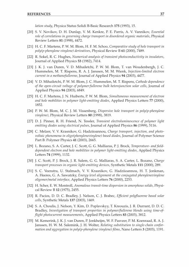
REFERENCES 37
lation study, Physica Status Solidi B-Basic Research 175 (1993), 15.
[20] S. V. Novikov, D. H. Dunlap, V. M. Kenkre, P. E. Parris, A. V. Vannikov, Essentialrole of correlations in governing charge transport in disordered organic materials, PhysicalReview Letters 81 (1998), 4472.
[21] H. C. F. Martens, P. W. M. Blom, H. F. M. Schoo, Comparative study of hole transport inpoly(p-phenylene vinylene) derivatives, Physical Review B 61 (2000), 7489.
[22] R. Sokel, R. C. Hughes, Numerical-analysis of transient photoconductivity in insulators,Journal of Applied Physics 53 (1982), 7414.
[23] J. K. J. van Duren, V. D. Mihailetchi, P. W. M. Blom, T. van Woudenbergh, J. C.Hummelen, M. T. Rispens, R. A. J. Janssen, M. M. Wienk, Injection-limited electroncurrent in a methanofullerene, Journal of Applied Physics 94 (2003), 4477.
[24] V. D. Mihailetchi, P. W. M. Blom, J. C. Hummelen, M. T. Rispens, Cathode dependenceof the open-circuit voltage of polymer:fullerene bulk heterojunction solar cells, Journal ofApplied Physics 94 (2003), 6849.
[25] H. C. F. Martens, J. N. Huiberts, P. W. M. Blom, Simultaneous measurement of electronand hole mobilities in polymer light-emitting diodes, Applied Physics Letters 77 (2000),1852.
[26] P. W. M. Blom, M. C. J. M. Vissenberg, Dispersive hole transport in poly(p-phenylenevinylene), Physical Review Letters 80 (1998), 3819.
[27] D. J. Pinner, R. H. Friend, N. Tessler, Transient electroluminescence of polymer lightemitting diodes using electrical pulses, Journal of Applied Physics 86 (1999), 5116.
[28] C. Melzer, V. V. Krasnikov, G. Hadziioannou, Charge transport, injection, and photo-voltaic phenomena in oligo(phenylenevinylene) based diodes, Journal of Polymer SciencePart B: Polymer Physics 41 (2003), 2665.
[29] L. Bozano, S. A. Carter, J. C. Scott, G. G. Malliaras, P. J. Brock, Temperature- and field-dependent electron and hole mobilities in polymer light-emitting diodes, Applied PhysicsLetters 74 (1999), 1132.
[30] J. C. Scott, P. J. Brock, J. R. Salem, G. G. Malliaras, S. A. Carter, L. Bozano, Chargetransport processes in organic light-emitting devices, Synthetic Metals 111 (2000), 289.
[31] S. C. Veenstra, U. Stalmach, V. V. Krasnikov, G. Hadziioannou, H. T. Jonkman,A. Heeres, G. A. Sawatzky, Energy level alignment at the conjugated phenylenevinyleneoligomer/metal interface, Applied Physics Letters 76 (2000), 2253.
[32] H. Scher, E. W. Montroll, Anomalous transit-time dispersion in amorphous solids, Physi-cal Review B 12 (1975), 2455.
[33] R. Pacios, D. D. C. Bradley, J. Nelson, C. J. Brabec, Efficient polyfluorene based solarcells, Synthetic Metals 137 (2003), 1469.
[34] S. A. Choulis, J. Nelson, Y. Kim, D. Poplavskyy, T. Kreouzis, J. R. Durrant, D. D. C.Bradley, Investigation of transport properties in polymer/fullerene blends using time-of-flight photocurrent measurements, Applied Physics Letters 83 (2003), 3812.
[35] M. Kemerink, J. K. J. van Duren, P. Jonkheijm, W. F. Pasveer, P. M. Koenraad, R. A. J.Janssen, H. W. M. Salemink, J. H. Wolter, Relating substitution to single-chain confor-mation and aggregation in poly(p-phenylene vinylene) films, Nano Letters 3 (2003), 1191.


3Photocurrent generation in bulk
heterojunction solar cells∗
Abstract
In this chapter, the photogeneration in organic donor/acceptor photovoltaiccells is discussed, with emphasis on the mechanism of charge dissociation andthe consequences of an unbalanced charge transport on photocurrent genera-tion. It is demonstrated that the photocurrent in conjugated polymer:fullereneblends is dominated by the dissociation efficiency of bound electron-hole pairsat the donor/acceptor interface. A model based on Onsager’s theory of gem-inate charge recombination is proposed, which explains the observed field-and temperature dependence of the photocurrent in polymer:fullerene blends.At room temperature only 60% of the generated bound electron-hole pairs inMDMO-PPV:PCBM blends are dissociated and contribute to the short-circuitcurrent, which constitutes a major loss mechanism in photovoltaic devices basedon this material system. With respect to the charge transport, it is demonstratedthat the photocurrent reaches the fundamental space-charge limit when the dif-ference in electron and hole mobility exceeds two orders of magnitude. The ex-perimental photocurrents reveal all the characteristics of a space-charge limitedphotocurrent; a one-half power dependence on voltage, a three-quarter powerdependence on light intensity, and a one-half power scaling of the voltage atwhich the photocurrent switches into full saturation with light intensity.
∗The main results of this chapter have been published as: (a) V. D. Mihailetchi, L. J. A. Koster,J. C. Hummelen, P. W. M. Blom, Physical Review Letters 93 (2004), 216601; (b) V. D. Mihailetchi, J.Wildeman, P. W. M. Blom, Physical Review Letters 94 (2005), 126602.
39
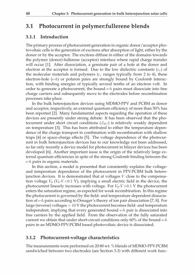
40 Chapter 3: Photocurrent generation in bulk heterojunction solar cells
3.1 Photocurrent in polymer:fullerene blends
3.1.1 Introduction
The primary process of photocurrent generation in organic donor/acceptor pho-tovoltaic cells is the generation of excitons after absorption of light, either by thedonor or by the acceptor. The excitons diffuse in either of the domains towardsthe polymer (donor)-fullerene (acceptor) interface where rapid charge transferwill occur [1]. After dissociation, a geminate pair of a hole at the donor andelectron at the acceptor is formed. Due to the low dielectric constants (ǫr) ofthe molecular materials and polymers (ǫr ranges typically from 2 to 4), theseelectron-hole (e-h) or polaron pairs are strongly bound by Coulomb interac-tion, with binding energies of typically several tenths of an electron volt. Inorder to generate a photocurrent, the bound e-h pairs must dissociate into freecharge carriers and subsequently move to the electrodes before recombinationprocesses take place.
In the bulk heterojunction devices using MDMO-PPV and PCBM as donorand acceptor, respectively, an external quantum efficiency of more than 50% hasbeen reported [2]. Many fundamental aspects regarding the operation of thesedevices are presently under strong debate: It has been observed that the pho-tocurrent under short circuit conditions (JSC) is relatively weakly dependenton temperature [3]. This has been attributed to either the temperature depen-dence of the charge transport in combination with recombination with shallowtraps [4] or space-charge effects [5]. The voltage dependence of the photocur-rent in bulk heterojunction devices has to our knowledge not been addressed,so far only recently a device model for photocurrent in bilayer devices has beendeveloped [6]. Another important issue is the origin of the relatively large ex-ternal quantum efficiencies in spite of the strong Coulomb binding between thee-h pairs in organic materials.
In this section, a model is presented that consistently explains the voltage-and temperature dependence of the photocurrent in PPV:PCBM bulk hetero-junction devices. It is demonstrated that at voltages V close to the compensa-tion voltage V0 (V0-V <0.1 V), implying a small electric field in the device, thephotocurrent linearly increases with voltage. For V0-V >0.1 V the photocurrententers the saturation regime, as expected for weak recombination. In this regimethe photocurrent is governed by the field- and temperature dependent dissocia-tion of e-h pairs according to Onsager’s theory of ion pair dissociation [7, 8]. Forlarge (reverse) voltages > 10 V the photocurrent becomes field- and temperatureindependent, implying that every generated bound e-h pair is dissociated intofree carriers by the applied field. From the observation of the fully saturatedcurrent we obtain that under short-circuit conditions only 60% of the bound e-hpairs in an MDMO-PPV:PCBM based photovoltaic device is dissociated.
3.1.2 Photocurrent-voltage characteristics
The measurements were performed on 20:80 wt. % blends of MDMO-PPV:PCBMsandwiched between two electrodes (see Section 3.3) with different work func-

3.1. Photocurrent in polymer:fullerene blends 41
0.5 0.6 0.7 0.8 0.9
-20
-10
0
10
20
VOC
V0
JD
JL
Jph=JL-JD
J [A
/m
2 ]
V [V]
Figure 3.1: Current density under illumination (JL), in the dark (JD), and calculated net
photocurrent (Jph); Jph=JL-JD . The arrows indicate the open-circuit voltage (VOC ) and
the compensation voltage (V0) determined when the Jph=0.
tion to generate an internal electric field, necessary to separate the photogener-ated charges. The devices were illuminated by a white light halogen lamp withan intensity of 800 W/m2, in inert (N2) atmosphere. A reverse voltage sweepfrom 1 V down to -15 V has been applied and the current density under illumi-nation (JL) has been recorded for a temperature range of 210 K - 295 K. In orderto determine the net photocurrent, the current density in the dark (JD) was alsorecorded. The experimental photocurrent is given by Jph=JL-JD. From the re-sulting Jph-V characteristics the compensation voltage (V0) at which Jph=0 wasdetermined, as is shown in the Figure 3.1.
3.1.3 The origin of the field-dependent (reverse bias)photocurrent
In Figure 3.2 Jph is plotted, at room temperature, on a double logarithmic scaleagainst the effective voltage across the device, given by V0-V . For a small effec-tive voltage (V0-V <0.1 V) the photocurrent increases linearly with the effectivevoltage, which has not been noticed before, and then tends to saturate. At higherreverse voltage (V0-V >1 V) the photocurrent further increases with increasingvoltage. In order to qualitatively understand this behavior, let us first considerthe situation in which recombination of free charge carriers as well as space-charge effects can be neglected. In that case the internal field in the device isgiven by E=(V0-V )/L, where V is the applied voltage. Without recombinationthe photocurrent through the external circuit is [9]:
Jph = qGL, (3.1)
where q is the electric charge, G the generation rate of e-h pairs, and L the thick-ness of the active layer. Thus in case of no recombination and a constant gener-ation rate G of e-h pairs Jph is independent of V , as shown in Figure 3.2 by thedotted line. However, Sokel and Hughes (SH) [10] pointed out that this result

42 Chapter 3: Photocurrent generation in bulk heterojunction solar cells
0.01 0.1 1 101
10
J ph [
A/
m2 ]
V0-V [V]
driftdiffusion
Figure 3.2: Room temperature Jph-V characteristics of an MDMO-PPV:PCBM 20:80 de-
vice as a function of effective applied voltage (V0-V ) (open circles), for a device with
thickness of 120 nm. The solid line represent calculated photocurrent from Equation 3.2
using G=1.56×1027 m−3s−1, whereas, the dotted line represent drift current calculated
from the Equation 3.1 using the same G.
is incorrect at low bias voltages because diffusion currents have been neglected.Using the same approximation as above, but including diffusion, SH found ananalytical solution for the photocurrent:
Jph = qGL
[
exp(qV/kBT ) + 1
exp(qV/kBT ) − 1− 2kBT
qV
]
, (3.2)
where qGL is the saturated photocurrent, kB is the Boltzmann constant and Tis the temperature, respectively. The solutions of the Equations 3.1 and 3.2 areshown schematically in Figure 3.2 together with the experimental data. Usinga G of 1.56 × 1027 m−3s−1, Equation 3.2 fits the experimental data at low effec-tive fields, indicating that diffusion plays an important role in the experimentalphotocurrent. It should be noted that the photocurrent given by Equation 3.2 isindependent of the mobility of either electrons or holes, since for none or veryweak recombination the carrier lifetime will always exceed the transit time.
It appears from Figure 3.2 that for effective voltages exceeding 1 V the ex-perimental photocurrent does not saturate at qGL but gradually increases forlarger effective voltages. An important process which has not been taken intoaccount into the Equations 3.1 and 3.2 is that not all the photogenerated bound e-h pairs (represented by Gmax) dissociate into free charge carriers. Only a certainfraction of Gmax is dissociated into free charge carriers, depending on field andtemperature, and therefore contributes to the photocurrent Jph. Consequently,the generation rate G of free charge carriers can be described by:
G(T,E) = GmaxP (T,E), (3.3)
where P (T,E) is the probability for charge separation at the donor/acceptorinterface.

3.1. Photocurrent in polymer:fullerene blends 43
3.1.4 A model for charge carriers dissociation atdonor/acceptor interface
The photogeneration of free charge carriers in low-mobility materials has firstbeen explained by the geminate recombination theory of Onsager [7, 8]. On-sager calculated the probability that a pair of oppositely charged ions in a weakelectrolyte, that undergo a Brownian random walk under the combined influ-ence of their mutual Coulomb attraction and external electric field, would es-cape recombination. An important addition to the theory has been made byBraun [11], who stressed the importance of the fact that the bound e-h pair(or charge transfer state) has a finite lifetime, as schematically depicted in Fig-ure 3.3. The bound e-h pair, formed after the dissociation of an exciton at thedonor/acceptor interface, can either decay to the ground state with a rate con-stant kF or separates into free carriers with an electric-field dependent rate con-stant kD(E). The decay rate (kF ) is dominated by phonon-assisted non radiativerecombination [12]. Once separated, the charge carriers can again form a boundpair with a rate constant kR, as shown schematically in Figure 3.3. Consequently,free carriers which are captured into bound pairs may dissociate again duringthe lifetime of the bound pair. Therefore, long lived charge transfer states act asa precursor for free charge carriers.
It has been demonstrated that after generation, bound e-h pairs in PPV:PCBMblends can still be detected after microseconds and even milliseconds, depend-ing on temperature [13, 14]. Furthermore, Onsager’s theory as discussed herewas extensively applied in the past to describe photogeneration in pure and sen-sitized conjugated polymers [15, 16]. It should be noted that Onsager’s modeldescribes charge dissociation in three dimensions. This is also applicable to bulkheterojunction cells since the length scale of morphology, typically two times theexciton diffusion length (10-15 nm), is in the order of Onsager radius of 17 nm.In Braun’s model the probability that a bound polaron pair dissociates into freecharge carries at a given electric field E and temperature T is given by:
P (T,E) =kD(E)
kD(E) + kF. (3.4)
Based on Onsager theory for field-dependent dissociation rate constants forweak electrolytes [7, 8], Braun derives kD(E) for dissociation of a bound pair
Figure 3.3: Schematic diagram of charge carrier separation at interface between polymer
(donor; D) and fullerene (acceptor; A).

44 Chapter 3: Photocurrent generation in bulk heterojunction solar cells
to be [11]:
kD(E) = kR3
4πa3e−
EB
kBT
[
1 + b +b2
3+
b3
18+
b4
180+ · · ·
]
, (3.5)
with a the initial separation of bound e-h pair at the interface, b=q3E/8πǫ0ǫrk2BT 2,
and EB the e-h pair’s binding energy. For low mobility semiconductors electron-hole recombination is given by Langevin: kR=q〈µ〉/ǫ0〈ǫr〉, where 〈ǫr〉 is spatiallyaveraged dielectric constant and 〈µ〉 the spatially averaged sum of electron andhole mobilities. Furthermore, in disordered materials as conjugated polymersand fullerenes it is unlikely that all donor/acceptor separations (a) would bethe same [17]. As a consequence, Equation 3.4 should be integrated over a dis-tribution of separation distances
P (T,E) = NF
∫ ∞
0
P (x, T,E)F (x)dx, (3.6)
where P (x, T,E) is the probability that an electron and hole generated at a dis-tance x, temperature T , and field E, will escape recombination; F (x) is a distri-bution function of donor-acceptor separations, and NF is a normalization factor
for the function F (x). The F (x) was assumed to be F (x) = x2e−x2/a2
, withNF = 4/π1/2a3 [17]. The bulk dielectric constant is εr=3.4 (which was taken asthe spatial average dielectric constant of PPV and PCBM). The final parametersrequired in the model are the mobilities of the charge carriers in the 20:80 blendsof MDMO-PPV:PCBM, which have been determined (in Chapter 2 of this thesis)to be µe=2.0 × 10⁻⁷ m2/Vs and µh=1.4 × 10⁻⁸ m2/Vs, at room temperature.
Combining Equations 3.3 and 3.6 the generation rate of producing free elec-trons and holes in blends of MDMO-PPV:PCBM for any temperature and elec-tric field can be calculated. It should be noted that Equation 3.3 involves onlytwo adjustable parameters: the initial separation of e-h pairs a, and the groundstate recombination rate kF , since all the other parameters were experimentallydetermined.
3.1.5 Comparing the model with the experimentalphotocurrent
Figure 3.4(a) (solid lines) shows the calculated photocurrent from Equation 3.1as a function of temperature, including the calculated field-dependent gener-ation rate G(T,E). Using a=1.3 nm, and a room temperature recombinationlifetime k−1
F =1 µs, the calculations consistently describe the field- and temper-ature dependence of the experimental data in the saturation regime (V0-V >0.3V). In the inset of Figure 3.4(a) the spatial distribution F (x) is shown for a=1.3nm corresponding to a mean e-h separation distance of typically 1.5 nm. InFigure 3.4(b) the (normalized) temperature dependence of the predicted- andexperimental photocurrent is plotted, for two different effective voltages of 0.01V and at short-circuit. The excellent agreement at both voltages demonstratesthat the activation energy of the photocurrent is completely dominated by therate of producing free electrons and holes (G) from the internal donor/acceptor

3.1. Photocurrent in polymer:fullerene blends 45
0.1 1 101
10
(a)
0.0 0.7 1.4 2.1 2.80.00.20.40.6
F(x)
x [nm]
295 K270 K250 K230 K210 K
J ph [A
/m2 ]
V0-V [V]3.4 3.6 3.8 4.0 4.2 4.4 4.6 4.8
0.2
0.4
0.6
0.8
1 (b)
Jph
/Jph
(295 K)
G/G(295 K)
∆=35.4 meV
∆=94.1 meV
J ph/J
ph(2
95
K),
G/G
(29
5 K
)
1000/T [K-1
]
Figure 3.4: (a) Temperature dependence of the photocurrent (symbols) versus effective
applied voltage (V0-V ) for a device of 100 nm thickness. The solid line represents the cal-
culated photocurrent from Equation 3.1 using field dependent generation rate G(T, E).
The inset shows the spatial distribution F (x) for a=1.3 nm. (b) Normalized experimen-
tally photocurrent (Jph) and normalized calculated generation rate [G(T, E)] from Figure
3.4(a), as a function of 1/T, taken in linear regime at 0.01 V (full symbols) and at short
circuit (empty symbols). The activation energies are written on the figure.
interface. It should be noted that the activation energy of G [shown in Figure3.4(b)] arises from the combined effect of the distribution of binding energies,the temperature dependence of both charge carrier mobility and decay rate k−1
F
as well as the effect of applied field, and therefore it does not reflect directly thebound e-h pair activation energy. As shown in Figure 3.4(a) at high effectivevoltages of typically 10 V the photocurrent saturates and becomes field- andtemperature independent. At these voltages all bound e-h pairs are separatedand the maximum photocurrent Jsat=qGmaxL is reached. By comparing thephotocurrent with the experimentally observed Jsat the dissociation efficiencycan be read directly from Figure 3.4(a). Under short-circuit conditions (V=0 V)only 60% of the bound e-h pairs dissociate, and at the maximum-power-point(V=0.64 V) this efficiency even further decreases to 52%. This incomplete disso-ciation of generated bound e-h pairs under operating conditions is therefore amain loss mechanism in solar cells based on PPV:PCBM blends.
As a next step, the generation rate G(T,E) is combined with Equation 3.2, asshown in Figure 3.5 by the dotted line, for 295 K. It is observed that this approachunderestimates the photocurrent in the low voltage regime. This apparent dis-crepancy arises from the fact that the analytical model has been deduced forblocking contacts [10]. However, in case of Ohmic contacts (as the devices pre-sented here), the internal electric field in the device is slightly modified due tothe band bending created by the accumulation of the charge carries at the inter-face. This effect is negligible at high reverse bias (in the saturation regime), butit has a significant effect at voltage close to V0 (in the linear regime). Therefore,the use of Equation 3.2 together with G(T,E) will not entirely fit the experimen-tal data of the devices with Ohmic contacts. Furthermore, the analytical modeldoes not include the effects of space charge and recombination. Therefore, we

46 Chapter 3: Photocurrent generation in bulk heterojunction solar cells
0.01 0.1 1 101
10
295 K
250 K
J ph [
A/m
2]
V0-V [V]
Figure 3.5: Experimental photocurrent (Jph) as a function of effective applied voltage
(V0-V ) of MDMO-PPV:PCBM 20:80 device (symbols), at 295 and 250 K. The solid line
represents the numerical calculation including diffusion, field dependent of generation
rate G(T, E) and recombination, for a device with thickness of 120 nm. The dotted line
represents calculated Jph from Equation 3.2 using G(T, E), at 295 K.
have developed an exact numerical model that calculates the steady-state chargedistributions within the active layer with Ohmic contacts by solving Poisson’sequation and the continuity equations, including diffusion and recombinationof charge carriers at donor/acceptor interface. This numerical model describesthe full current-voltage characteristics in the dark and under illumination, in-cluding the field dependent generation rate G(T,E) [18]. Figure 3.5 shows theexperimental photocurrent (symbols) together with the numerical calculation(solid lines) for two different temperatures. At both temperatures, using thesame parameters as presented above, the calculated photocurrent fits the exper-imentally data over the entire voltage range.
3.1.6 Conclusion
In this section, the photocurrent in 20:80 blends of MDMO-PPV:PCBM solarcells has been interpreted using a model based on Onsager’s theory of geminatecharge recombination. The model explains the field- and temperature depen-dence of the photocurrent in a large voltage regime. The long lifetime of 1 µsis a precursor for the high external quantum efficiencies observed in MDMO-PPV:PCBM blends. Under short-circuit conditions, at room temperature, only60% of the bound e-h pairs are separated and contribute to the photocurrent.
3.2 Space-charge limitation in organic solar cells
3.2.1 Introduction
When a semiconductor is exposed to photons with an energy larger than theband gap, charge carriers are produced. With a built-in field or an externally

3.2. Space-charge limitation in organic solar cells 47
applied bias these charge carriers can be separated, thereby producing a pho-tocurrent in an external circuit. The efficiency of photocurrent generation de-pends on the balance between charge carrier generation, recombination, andtransport. The extraction of photogenerated electrons and holes from a semi-conductor has been treated by Goodman and Rose [9]. With non-injecting con-tacts the external photocurrent becomes saturated when all photogenerated freeelectrons and holes are extracted from the semiconductor. This implies that themean electron and hole drift lengths we(h)=µe(h)τe(h)E are equal or longer thanthe specimen thickness L; with µe(h) the charge carrier mobility of electrons(holes), τe(h) the charge carrier lifetime and E the electric field, respectively.In this case no recombination occurs and the saturated photocurrent densityis given by Jsat
ph =qGL [9]. However, as is shown in Section 2.1, if either we<L orwh<L or both are smaller than L, space-charge will form and recombination offree charge carriers becomes significant. In the following, this specific case willbeen analyzed with more details.
3.2.2 Goodman and Rose approximation
Suppose that the e-h pairs are photogenerated uniformly throughout the spec-imen and that the charge transport is strongly unbalanced, meaning that we 6=wh. As is demonstrated in Section 2.1, in a semiconductor with wh≪we andwh<L, the holes will accumulate to a greater extent in the device than the elec-trons, altering the electric field. As a consequence, the electric field increases inthe region (L1) near the anode, enhancing the extraction of holes, as is shownschematically in Figure 2.1(b). In Section 2.1 it has been shown that if wh≪we,the length of the region L1 is given by the mean hole drift length (L1=
√µhτhV1).
Since almost the entire voltage V drops on the region of hole accumulation(V1≈V ) and the photocurrent generated in this region is substantially the totalcurrent, it follows directly that [9]:
Jph = qGL1 = qG(µhτh)1/2V 1/2. (3.7)
It is evident that in the region L1 the accumulated holes are not neutralizedby an equal density of electrons, which results in a build-up of positive space-charge. Goodman and Rose pointed out that there is a fundamental limit to beexpected for the build-up of space-charge in a semiconductor at high intensities;The electrostatic limit of hole accumulation is reached when the photocurrentgenerated in this region, Jph=qGL1, is equal to the space-charge limited current:
JSCL =9
8ε0εrµh
V 21
L31
, (3.8)
where ε0εr is the dielectric permittivity. By equating qGL1 with Equation 3.8 itfollows that the length of the region L1 in this space-charge limited (SCL) regimeis given by:
L1 = (9ε0εrµh/8qG)1/4V1/21 . (3.9)

48 Chapter 3: Photocurrent generation in bulk heterojunction solar cells
Since V1≈V , the maximum electrostatically allowed photocurrent that can beextracted from the device is [9]:
Jph = q(9ε0εrµh
8q
)1/4
G3/4V 1/2. (3.10)
Comparison of Equations 3.7 and 3.10 show that both in the absence and pres-ence of the space-charge limitation Jph scales with the square-root of the appliedvoltage and is governed by the slowest charge carrier mobility, although thephysical reasons of this are distinctly different. Experimentally, both regimescan be discriminated by investigating their dependence on G. To our knowl-edge, the existence of SCL photocurrents has not been demonstrated experi-mentally in semiconductors so far.
3.2.3 Experimental evidence
In order to observe SCL photocurrents a semiconductor should fulfil a numberof requirements: First, the amount of photogenerated charge carriers should belarge, meaning a large G and a long carrier lifetime τe(h) after dissociation ofthe e-h pairs. Furthermore, the charge transport should be strongly unbalanced,leading to the formation of space-charge regions. Finally, the slowest charge car-rier should have a low mobility such that the photocurrent can reach the SCLcurrent inside the space-charge region. A material system that fulfills most ofthese demands are blends of conjugated polymers (electron donor) and fullerenemolecules (electron acceptor) [19]. In these blends light absorption leads to theproduction of excitons that subsequently dissociate at the internal interface byan ultrafast electron transfer (≈45 fs) from excited polymer to fullerene [1]. Sincethe created electrons and holes are spatially separated the back-transfer processis very slow leading to long-lived charge carriers, in the microsecond to mil-lisecond range [13, 14]. In combination with the large internal donor/acceptorinterface these bulk heterojunctions enable a large generation rate of long-livedcharge carriers.
As is explained in the previous section, the important quantity which de-termines the formation of space-charge in photoconductors, is the difference inthe µτ product of electrons and holes. The most investigated system of poly-mer/fullerene solar cells are blends of MDMO-PPV and PCBM. The main re-combination process found in these devices is bimolecular recombination ofphotogenerated free electrons and holes (as discussed in Section 3.1), resultingin an equal electron and hole lifetime. Therefore, a large mobility difference be-tween electrons and holes is required for the generation of a SCL photocurrent inthis system. However, it turns out that the hole mobility of MDMO-PPV insidethe blend is enhanced by a factor of 400 as compared with the pure material (seeSection 2.3). The resulting mobility difference of only one order of magnitudeis not sufficient to induce a SCL photocurrent. As demonstrated in Section 2.3,when symmetrical substituted PPV is used (such as BEH1BMB3-PPV), the holemobility in polymer phase is hardly affected by the presence of PCBM, resultingin an increased mobility difference between electrons and holes in the blend.The measurements here were performed on 20:80 weight percentage blends of
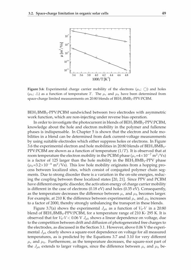
3.2. Space-charge limitation in organic solar cells 49
3.4 3.6 3.8 4.0 4.2 4.4 4.6 4.8
10-11
10-10
10-9
10-8
10-7
µ [m
2 /V
s]
1000/T [K-1]
Figure 3.6: Experimental charge carrier mobility of the electrons (µe; ©) and holes
(µh; ) as a function of temperature T . The µe and µh have been determined from
space-charge limited measurements on 20:80 blends of BEH1BMB3-PPV:PCBM.
BEH1BMB3-PPV:PCBM sandwiched between two electrodes with asymmetricwork function, which are non-injecting under reverse bias operation.
In order to investigate the photocurrent in blends of BEH1BMB3-PPV:PCBM,knowledge about the hole and electron mobility in the polymer and fullerenephases is indispensable. In Chapter 5 is shown that the electron and hole mo-bilities in a blend can be determined from dark current-voltage measurementsby using suitable electrodes which either suppress holes or electrons. In Figure3.6 the experimental electron and hole mobilities in 20:80 blends of BEH1BMB3-PPV:PCBM are shown as a function of temperature (1/T ). It is observed that atroom temperature the electron mobility in the PCBM phase (µe=4×10⁻⁷ m2/Vs)is a factor of 125 larger than the hole mobility in the BEH1BMB3-PPV phase(µh=3.2×10⁻⁹ m2/Vs). This low hole mobility originates from a hopping pro-cess between localized sites, which consist of conjugated polymer chain seg-ments. Due to strong disorder there is a variation in the on-site energies, reduc-ing the coupling between these localized states [20, 21]. Since PPV and PCBMhave different energetic disorder, the activation energy of charge carrier mobilityis different in the case of electrons (0.18 eV) and holes (0.35 eV). Consequently,as the temperature decreases the difference between µe and µh becomes larger.For example, at 210 K the difference between experimental µe and µh increasesto a factor of 2000, thereby strongly unbalancing the transport in these blends.
Figure 3.7(a) shows the experimental Jph as a function of V0-V in a 20:80blend of BEH1BMB3-PPV:PCBM, for a temperature range of 210 K- 295 K. It isobserved that for V0-V < 0.06 V Jph shows a linear dependence on voltage, dueto the competition between drift and diffusion of photogenerated free charges tothe electrodes, as discussed in the Section 3.1. However, above 0.06 V the experi-mental Jph clearly shows a square-root dependence on voltage for all measuredtemperatures, as is predicted by the Equations 3.7 and 3.10 for very differentµe and µh. Furthermore, as the temperature decreases, the square-root part ofthe Jph extends to larger voltages, since the difference between µe and µh be-

50 Chapter 3: Photocurrent generation in bulk heterojunction solar cells
0.01 0.1 1 101
10 295 K270 K250 K230 K210 K
J ph [A
/m2 ]
V0-V [V]
(a)
0.01 0.1 1 100.1
1
10
(b)
J ph [A
/m2 ]
V0-V [V]
L=275 nmT=210 K
Vsat
Figure 3.7: (a) Temperature dependence of the photocurrent (symbols) in a 20:80 blend
of BEH1BMB3-PPV:PCBM versus effective applied voltage (V0-V ) for a device of 275
nm thickness illuminated at an intensity of 800 W/m2. The solid lines represent the
square-root dependence of the photocurrent Jph on effective voltage, used here as a guide
for the eye. (b) Incident light power (ILP) dependence of the photocurrent (Jph) versus
the effective voltage (V0-V ) measured at T=210 K. The solid (thick) lines represent the
calculated Jph from Equation 3.10 using µh=1.2×10⁻¹¹ m2/Vs, εr=2.6 and G∝ILP, where
ILP was varied from 800 to 60 W/m2. The arrow indicates the voltage (Vsat) at which
Jph shows the transition to the saturation regime.
comes larger. At even larger voltages (≈0.8 V at 295 K) the Jph shows a cleartransition to the saturation regime, where it becomes limited by the field- andtemperature dependence of the generation rate G(E, T ) (Equation 3.3). Theseresults are distinctly different than in the case of MDMO-PPV:PCBM blends,where no square-root dependence of Jph is observed, as a result of the more bal-anced transport (see Section 3.1). The important question is whether Jph fromFigure 3.7(a) is limited by the space-charge (Equation 3.10) or by the mobility-lifetime product given by Equation 3.7. The unique test to distinguish betweenthe two processes is to investigate the dependence of Jph on G, since a differentdependence is predicted by Equations 3.7 and 3.10. A direct way to change theamount of photogenerated charge carriers is to vary the light intensity. We havedemonstrated in the Section 3.1 that in the absence of SCL the Jph in reversebias is described by Jph=qG(E, T )L. Furthermore, for these non-SCL devicesJph closely follows a linear dependence with light intensity [22, 23]. Combiningthese two observations it follows that G is proportional with light intensity inthese type of devices. Therefore, the SCL photocurrent is expected to scale witha 3/4 power dependence on light intensity (Equation 3.10).
Figure 3.7(b) shows the Jph-(V0-V ) characteristics, of the same device fromFigure 3.7(a), as a function of incident light power (ILP), measured at 210 K. Thistemperature was chosen because the Jph shows the largest square-root regime,but the same effect is present also at room temperature. The ILP was varied from800 W/m2 (upper curve) down to 60 W/m2 using a set of neutral density filters.It appears from Figure 3.7(b) that the Jph shows weaker light intensity depen-dence in the square-root regime as compared with the saturation regime. Figure
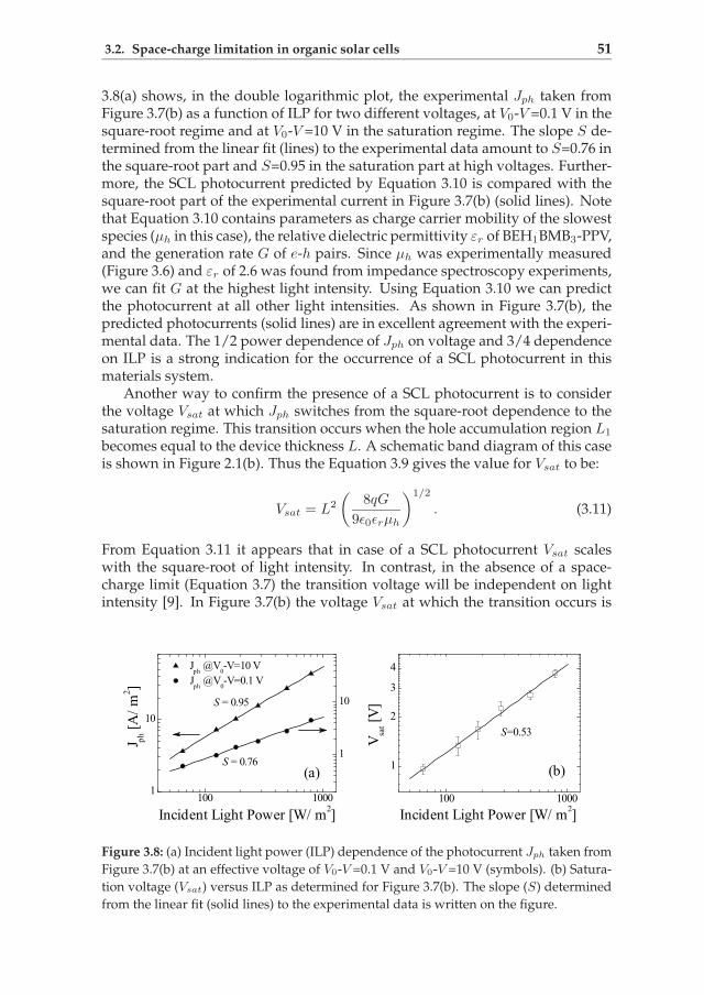
3.2. Space-charge limitation in organic solar cells 51
3.8(a) shows, in the double logarithmic plot, the experimental Jph taken fromFigure 3.7(b) as a function of ILP for two different voltages, at V0-V =0.1 V in thesquare-root regime and at V0-V =10 V in the saturation regime. The slope S de-termined from the linear fit (lines) to the experimental data amount to S=0.76 inthe square-root part and S=0.95 in the saturation part at high voltages. Further-more, the SCL photocurrent predicted by Equation 3.10 is compared with thesquare-root part of the experimental current in Figure 3.7(b) (solid lines). Notethat Equation 3.10 contains parameters as charge carrier mobility of the slowestspecies (µh in this case), the relative dielectric permittivity εr of BEH1BMB3-PPV,and the generation rate G of e-h pairs. Since µh was experimentally measured(Figure 3.6) and εr of 2.6 was found from impedance spectroscopy experiments,we can fit G at the highest light intensity. Using Equation 3.10 we can predictthe photocurrent at all other light intensities. As shown in Figure 3.7(b), thepredicted photocurrents (solid lines) are in excellent agreement with the experi-mental data. The 1/2 power dependence of Jph on voltage and 3/4 dependenceon ILP is a strong indication for the occurrence of a SCL photocurrent in thismaterials system.
Another way to confirm the presence of a SCL photocurrent is to considerthe voltage Vsat at which Jph switches from the square-root dependence to thesaturation regime. This transition occurs when the hole accumulation region L1
becomes equal to the device thickness L. A schematic band diagram of this caseis shown in Figure 2.1(b). Thus the Equation 3.9 gives the value for Vsat to be:
Vsat = L2
(
8qG
9ǫ0ǫrµh
)1/2
. (3.11)
From Equation 3.11 it appears that in case of a SCL photocurrent Vsat scaleswith the square-root of light intensity. In contrast, in the absence of a space-charge limit (Equation 3.7) the transition voltage will be independent on lightintensity [9]. In Figure 3.7(b) the voltage Vsat at which the transition occurs is
1
10
100 1000
1
10
Jph @ V0-V=10 V
S = 0.76
J ph [A
/m2 ]
S = 0.95
(a)
Jph @ V0-V=0.1 V
Incident Light Power [W/ m2]100 1000
1
2
3
4
(b)
Incident Light Power [W/ m2]
Vsa
t [V]
S=0.53
Figure 3.8: (a) Incident light power (ILP) dependence of the photocurrent Jph taken from
Figure 3.7(b) at an effective voltage of V0-V =0.1 V and V0-V =10 V (symbols). (b) Satura-
tion voltage (Vsat) versus ILP as determined for Figure 3.7(b). The slope (S) determined
from the linear fit (solid lines) to the experimental data is written on the figure.

52 Chapter 3: Photocurrent generation in bulk heterojunction solar cells
determined from the crossover point of the square-root dependence and the ex-trapolated saturation part, as indicated by the arrow. From Figure 3.7(b) it isalready demonstrated that Vsat shows a clear variation with light intensity. InFigure 3.8(b) Vsat is plotted in double logarithmic scale as a function of ILP. Aslope S=0.51 is found, being in agreement with the space-charge limited predic-tion (of 0.5) from Equation 3.11. This is a further conformation that the pho-tocurrent in 20:80 blends of BEH1BMB3-PPV:PCBM devices is truly limited byspace-charge effects.
3.2.4 Analytical prediction for the conversion efficiency
The SCL photocurrent is the maximum electrostatically allowed current that canbe generated into the external circuit of any solar cell. A Jph limited by space-charge effect also has a strong impact on the power conversion efficiency ofthis type of solar cells. For a photovoltaic device (Figure 3.7) the output powerdensity is given by P (V )=Jph(VOC-V ) ·V , where VOC is the open-circuit voltage(VOC≈V0). For a device under space-charge limitation the Jph(VOC-V ) is givenby Equation 3.10. Thus P (V ) ∝ (VOC-V )1/2 · V , which reaches its maximum(Pmax) at V =Vmax=( 2
3 )VOC . Hence, from Equation 3.10 we obtain:
Pmax = qG3/4
(
9ǫ0ǫrµh
8q
)1/42
33/2V
3/2OC . (3.12)
The fill factor (FF) of the photovoltaic cells is calculated from the ratio:
FF =JmaxVmax
JSCVOC× 100%, (3.13)
where JmaxVmax=Pmax and JSC is the short-circuit current (applied voltage V =0 V). Combining Equations 3.10 and 3.12 gives the maximum possible value ofthe FF for a solar cell limited by the space-charge to be:
FF =2
33/2× 100% = 38.49%. (3.14)
From Figure 3.7 and Equation 3.11 it is observed that Jph is limited by the build-up of space-charge for effective voltages V0-V <Vsat, and is space-charge-freefor V0-V ≥Vsat. The JSC of the solar cells is given at the effective voltage of V0-V ≈VOC (which is ≈0.8 V for the experimental data presented here). Thus, forthe Vsat>VOC , the JSC will fall into the space-charge limitation (square-root de-pendence on V ) and it will approach a 3/4 light intensity dependence (Equation3.10). Consequently, the solar cell performance is fully limited by space-chargeeffect (Equations 3.12 and 3.14). In order to reduce the effect of the space-chargeon device performance, the Vsat should be strongly reduced (Vsat−→0 V). FromEquation 3.11 it is observed that Vsat is mostly influenced by the film thicknessL and the light intensity (or G). A device could be space-charge-free under nor-mal operation condition (1 Sun illumination), but become space-charge limitedat higher light intensity or in thicker films, as long as there is a difference be-tween electron and hole mobility to build-up the space-charge accumulation.

3.3. Experimental section 53
Equations 3.12 and 3.14 qualitatively predict the maximum electrostatic al-lowed FF and power conversion efficiency (η=100%×Pmax/ILP) of any solarcell limited by space-charge. It is important to note that for a quantitative analy-sis the effect of diffusion, recombination, field-dependent generation rate G(E)and the effect of a non uniform electric field should be taken into account. Forexample, as has been shown in this chapter, a linear dependence of Jph-(V0-V )characteristics is observed at very low effective voltages (close to V0 or VOC) dueto diffusion. Such a linear dependence increases the maximum attainable FF ofthe solar cell under space-charge limitation (Figure 3.7) to a value of approxima-tively 42%. A recent numerical model developed by Koster et al. incorporatesthese processes and a quantitative fit to the experimental data can be given [18].
3.2.5 Conclusion
In this Section, we demonstrated the existence of a fundamental limit of the pho-tocurrent in semiconductors. The photocurrent in 20:80 blends of BEH1BMB3-PPV:PCBM solar cell devices reaches this electrostatic limit already under nor-mal operational conditions (0.8 sun). The experimental photocurrents obey allfeatures characteristic for the space-charge limited regime: The photocurrent isproportional with a 1/2 power dependence on voltage and a 3/4 power of lightintensity. Furthermore, the saturation voltage varies as the one-half power ofthe light intensity. These results give further insight in the mechanism of photo-conduction in semiconductors and are valuable for the design of new materialsin organic photovoltaic devices.
3.3 Experimental section
Materials: The material used were MDMO-PPV synthesized via the Gilch-route, PCBM (received from University of Groningen), a 25:75 random copoly-mer of poly[2,5-bis(2‘-ethylhexyloxy)-co-2,5-bis(2‘-methylbutyloxy)-1,4-pheny-lene vinylene] (BEH1BMB3-PPV; for molecular structure see Figure 2.14), PE-DOT:PSS from Bayer AG (Baytron P VP Al 4083), LiF and Al from Aldrich. Glassplates (3 cm × 3 cm) covered with ≈160 nm patterned ITO resulting in 4 differ-ent device areas (0.1, 0.15, 0.33, 1 cm2) were used for device preparation.Device Preparation: The ITO covered glass substrates were wet-cleaned byrubbing with soap, rinsing with water, and ultrasonic cleaning in acetone andpropanol. The substrates were further UV-ozone treated and a layer of PE-DOT:PSS was subsequently spin-coated on the pre-cleaned ITO, using a Con-vac spin-coater. The PEDOT:PSS layer was dried at an elevated temperature.The samples were then inserted into a glove box filled with nitrogen. An ac-tive layer was then spin-coated using a Karl Suss spin-coater following by theevaporation of the metal top electrode which consist of a thin LiF (1 nm) layertoped with Al (100 nm) to complete the devices. The active layer consist eitherof a 20:80 weight percentage blend of MDMO-PPV:PCBM spin-coated from achlorobenzene solution (with a concentration of ≈3.3 mg PPV/mL), or by a 20:80weight percentage blend of BEH1BMB3-PPV:PCBM spin-coated from a ortho-

54 Chapter 3: Photocurrent generation in bulk heterojunction solar cells
dichlorobenzene solution (with a concentration of ≈8.0 mg PPV/mL). In orderto determine the electron and hole mobility in blends of BEH1BMB3-PPV:PCBM(Figure 3.6), the devices were prepared and characterized similar to that de-scribed in Section 5.5.Device Characterization: All measurements were performed under a nitro-gen atmosphere. J-V measurements were performed with a Keithley 2400Sourcemeter. In forward bias ITO electrode was positively biased. The de-vices were illuminated at the transparent ITO electrode using a halogen lampwith a spectral range of 400-850 nm calibrated using a Si diode. Light intensitydependence was measured by varying the light power using a set of neutraldensity filters with a constant optical density over the spectral range of the lightsource. Subsequently, the resulting spectrum of each filter-lamp combinationwas recorded and integrated over the absorption spectrum of the active layer,which gives the intensity. Therefore, the generation rate (G) of electron-holepairs is proportional to the light intensity (G∝ILP).

REFERENCES 55
References
[1] C. J. Brabec, G. Zerza, G. Cerullo, S. De Silvestri, S. Luzzati, J. C. Hummelen, S. Sari-ciftci, Tracing photoinduced electron transfer process in conjugated polymer/fullerene bulkheterojunctions in real time, Chemical Physics Letters 340 (2001), 232.
[2] S. E. Shaheen, C. J. Brabec, N. S. Sariciftci, F. Padinger, T. Fromherz, J. C. Hummelen,2.5% efficient organic plastic solar cells, Applied Physics Letters 78 (2001), 841.
[3] D. Chirvase, Z. Chiguvare, M. Knipper, J. Parisi, V. Dyakonov, J. C. Hummelen, Tem-perature dependent characteristics of poly(3 hexylthiophene)-fullerene based heterojunctionorganic solar cells, Journal of Applied Physics 93 (2003), 3376.
[4] I. Riedel, J. Parisi, V. Dyakonov, L. Lutsen, D. Vanderzande, J. C. Hummelen, Effectof temperature and illumination on the electrical characteristics of polymer-fullerene bulk-heterojunction solar cells, Advanced Functional Materials 14 (2004), 38.
[5] J. Nelson, Diffusion-limited recombination in polymer-fullerene blends and its influence onphotocurrent collection, Physical Review B 67 (2003), 155209.
[6] J. A. Barker, C. M. Ramsdale, N. C. Greenham, Modeling the current-voltage character-istics of bilayer polymer photovoltaic devices, Physical Review B 67 (2003), 075205.
[7] L. Onsager, Deviation from ohm’s law in weak electrolytes, Journal of Chemical Physics2 (1934), 599.
[8] L. Onsager, Initial recombination of ions, Physical Review 54 (1938), 554.
[9] A. M. Goodman, A. Rose, Double extraction of uniformly generated electron-hole pairsfrom insulators with noninjecting contacts, Journal of Applied Physics 42 (1971), 2823.
[10] R. Sokel, R. C. Hughes, Numerical-analysis of transient photoconductivity in insulators,Journal of Applied Physics 53 (1982), 7414.
[11] C. L. Braun, Electric-field assisted dissociation of charge-transfer states as a mechanism ofphotocarrier production, Journal of Chemical Physics 80 (1984), 4157.
[12] N. S. Sariciftci, A. J. Heeger, Reversible, metastable, ultrafast photoinduced electron-transfer from semiconducting polymers to buckminsterfullerene and in the correspondingdonor-acceptor heterojunctions, International Journal of Modern Physics B 8 (1994),237.
[13] T. Offermans, S. C. J. Meskers, R. A. J. Janssen, Charge recombination in a poly(para-phenylene vinylene)-fullerene derivative composite film studied by transient, nonresonant,hole-burning spectroscopy, Journal of Chemical Physics 119 (2003), 10924.
[14] I. Montanari, A. F. Nogueira, J. Nelson, J. R. Durrant, C. Winder, M. A. Loi, N. S.Sariciftci, C. Brabec, Transient optical studies of charge recombination dynamics in a poly-mer/fullerene composite at room temperature, Applied Physics Letters 81 (2002), 3001.
[15] T. K. Daubler, V. Cimrova, S. Pfeiffer, H. H. Horhold, D. Neher, Electric field and wave-length dependence of charge carrier photogeneration in soluble poly(p-phenylenevinylene)derivatives, Advanced Materials 11 (1999), 1274.
[16] S. Barth, H. Bassler, Intrinsic photoconduction in PPV-type conjugated polymers, Physi-cal Review Letters 79 (1997), 4445.
[17] T. E. Goliber, J. H. Perlstein, Analysis of photogeneration in a doped polymer system interms of a kinetic-model for electric-field-assisted dissociation of charge-transfer states, Jour-nal of Chemical Physics 80 (1984), 4162.

56 Chapter 3: Photocurrent generation in bulk heterojunction solar cells
[18] L. J. A. Koster, E. C. P. Smits, V. D. Mihailetchi, P. W. M. Blom, Device model forthe operation of polymer/fullerene bulk heterojunction solar cells, Physical Review B, 72(2005), 085205.
[19] C. J. Brabec, N. S. Sariciftci, J. C. Hummelen, Plastic solar cells, Advanced FunctionalMaterials 11 (2001), 15.
[20] H. C. F. Martens, P. W. M. Blom, H. F. M. Schoo, Comparative study of hole transport inpoly(p-phenylene vinylene) derivatives, Physical Review B 61 (2000), 7489.
[21] H. Bassler, Charge transport in disordered organic photoconductors - A monte-carlo simu-lation study, Physica Status Solidi B-Basic Research 175 (1993), 15.
[22] J. K. J. van Duren, X. N. Yang, J. Loos, C. W. T. Bulle-Lieuwma, A. B. Sieval,J. C. Hummelen, R. A. J. Janssen, Relating the morphology of poly(p-phenylene viny-lene)/methanofullerene blends to solar-cell performance, Advanced Functional Materials14 (2004), 425.
[23] P. Schilinsky, C. Waldauf, C. J. Brabec, Recombination and loss analysis in polythiophenebased bulk heterojunction photodetectors, Applied Physics Letters 81 (2002), 3885.

4Variation of the metal top electrode in bulk
heterojunction solar cells∗
Abstract
The performance of bulk heterojunction solar cells based on blends of conju-gated polymers and fullerenes is known to be critically dependent on the natureof the metal top electrode. In contrast to the present understanding, it is demon-strated that the open-circuit voltage (VOC) of the solar cells with non-Ohmiccontacts is determined by the work function difference of the electrodes. ForOhmic contacts the VOC is governed by the LUMO and HOMO levels of theacceptor and donor, respectively, which pin the Fermi levels of the cathode andanode. The band bending created by accumulated charges at both interfacesdue to Ohmic contacts produce a considerable loss in VOC of ≈0.38 V at roomtemperature. Furthermore, the photocurrent obtained from the active layer of asolar cell, with a different metal work function, such as lithium fluoride toppedwith aluminum, silver, gold, or palladium, shows a universal behavior whenscaled against the effective voltage across the device. Consequently, for anygiven metal, only the device’s VOC is required in order to be able to predict theremaining solar cell parameters.
∗The main results of this chapter have been published as: (a) V. D. Mihailetchi, P. W. M. Blom,J. C. Hummelen, M. T. Rispens, Journal of Applied Physics 94 (2003), 6849; (b) V. D. Mihailetchi, L. J. A.Koster, P. W. M. Blom, Applied Physics Letters 85 (2004), 970.
57

58 Chapter 4: Variation of the metal top electrode in bulk heterojunction solar cells
4.1 Electrode dependence of the open-circuit
voltage
4.1.1 Introduction
The essential parameters which determine the power conversion efficiency ofthin film photovoltaic devices are the short-circuit current (JSC), the open-circuit voltage (VOC), and the fill factor (FF). It has been shown that the JSC issensitive to the film morphology, solvent type, or deposition method [1, 2]. For-mation of a bulk heterojunction by mixing the polymer (donor) and the fullerene(acceptor) lead to an enhancement of JSC due to an increased interface area forcharge separation. However, the JSC is still much lower than the typical valuesreported for inorganic photovoltaic devices. This lower photocurrent is mainlydue to the spectral mismatch between the sunlight and the absorption spectrumof the polymers (and fullerenes) used, as well as the limited transport of the sep-arated charge carriers to the electrodes due to the low charge carrier mobility inorganic materials.
On the other hand, organic solar cells produce quite respectable open-circuitvoltages. It has been demonstrated that for a photodiode, based on a single layerof a conjugated polymer, the VOC scales with the work function difference be-tween electrodes, and thus follows the metal-insulator-metal (MIM) model [1].In bilayer devices made by electron- and hole-accepting polymers, the VOC alsoscales linearly with the work function difference, however, with an additionalcontribution depending on the light intensity [3]. This contribution is due to theaccumulation of charge carriers at the organic/organic interface, giving rise to adiffusion current which must be compensated by a drift current at open-circuit.In bulk heterojunction (BHJ) solar cells, a linear correlation of the VOC with thevariation of the oxidation potential of the donor conjugated polymers [4] and re-duction potential of the acceptor [5, 6], has been reported. The fact that a slope
Figure 4.1: Schematic variation of VOC with acceptor strength (solid double headed ar-
row, VOC1) or/and electrode work function (dotted arrow, VOC2), in a donor/acceptor
bulk heterojunction solar cell. The electron transfer, occurring at the donor/acceptor in-
terface after light excitation, is indicated by the bent arrow.

4.1. Electrode dependence of the open-circuit voltage 59
unity was obtained indicates a strong coupling of VOC to the reduction strengthof the acceptors or oxidation potential of the donors. In case of Ohmic contacts,meaning that the negative and positive electrodes match the LUMO level of theacceptor and the HOMO level of the donor, respectively, such a correlation isexpected. The maximum VOC for this case is schematically indicated by VOC1 inFigure 4.1 and is thus governed by the bulk material properties. In case of non-Ohmic contacts, as is depicted in Figure 4.1, a reduced VOC with magnitudeVOC2 is expected, according to the MIM model. However, a very weak variationof the VOC of only 160 meV has been observed when varying the work functionof the negative electrode from 5.1 eV (Au) to 2.9 eV (Ca) [5, 6]. This deviationfrom the MIM model has been explained by pinning of the electrode Fermi levelto the reduction potential of the fullerene. For the design of future solar cells itis important to understand whether the VOC of BHJ devices can be adapted bythe choice of the electrodes and whether the VOC is a bulk property (as shownby solid arrow in Figure 4.1) or an electrode property (shown by dotted line inFigure 4.1), or a combination of both. In this study we first investigated the elec-tronic properties of various negative top electrodes on PCBM-only devices. Theinformation regarding the alignment of the Fermi level of the various electrodeson PCBM is then applied to the experimental data on MDMO-PPV:PCBM basedsolar cells. We demonstrate that the VOC of the cells can be varied over morethan 0.5 V by changing the work function of the top electrode.
4.1.2 Open-circuit voltage of pristine fullerene devices
In order to study a possible pinning of the Fermi level of the negative top elec-trode on PCBM, devices consisting of a single layer of PCBM were investigatedas a reference. The devices were produced on top of a glass substrate, cov-ered by indium-tin-oxide (ITO). As a bottom electrode, a hole transport layerof PEDOT:PSS was spin-coated under ambient condition, then the layer wasdried in the oven. Subsequently, PCBM was spin cast from a chlorobenzene so-lution. Finally, gold (Au, 50 nm), silver (Ag, 80 nm), or lithium fluoride (LiF, 1nm)/aluminum (Al, 100 nm) were thermally evaporated (pressure< 10−6 mbar)as the top electrode.
When a metal is making intimate contact with a semiconductor or insula-tor, at equilibrium, the Fermi levels in the two materials will coincide. If thework function of the metal is higher then the LUMO level of the semiconduc-tor, an interface barrier ϕb for electrons will be formed [Figure 4.2(a)]. As indi-cated in Figure 4.2(a) for two of these blocking contacts, the VOC of the device isgiven by difference between the metals work functions. For the PCBM devicesa schematic diagram is shown in Figure 4.2(a), where M2 is the bottom elec-trode (PEDOT:PSS, ϕM2=5.2 eV) and M1 is the evaporated top electrode (Ag,Au, LiF/Al). From Figure 4.2(a) it appears that
ϕb + qVOC = ϕM2 − LUMO, (4.1)
where q is the electric charge and LUMO is the position of the PCBM LUMOlevel with respect to vacuum (3.7 eV), respectively. Equation 4.1 indicates thatfor a given bottom electrode work function (in this case PEDOT:PSS), the sum

60 Chapter 4: Variation of the metal top electrode in bulk heterojunction solar cells
Figure 4.2: Schematic band diagram of a metal-insulator-metal (MIM) device with
non-Ohmic contact for electrons and holes (a), and electron Ohmic contact (b). Before
metal contact (upper image) and after contact and under short-circuit condition (lower
image). The ϕb and ∆Vb are injection barrier height for electrons at a non-Ohmic contact
and the voltage loss at an Ohmic contact, respectively. ϕM1 and ϕM2 are the metal work
functions.
of electron barrier height and VOC is constant for different top electrodes. It isimportant to note that in our PCBM devices both ϕb and VOC can be indepen-dently determined from J-V measurements. The barrier heights for electronsgoing from Ag and Au into the LUMO level of PCBM have been determinedby investigation of the injection limited electron current (ILC). It was recentlydemonstrated that the injection limited current is well described by hopping ofcharge carriers from the Fermi level of the metal into energetically disorderedlocalized states of the organic semiconductor [7, 8]. According to this hopping-based model, the ILC is determined by four parameters [7, 8]; the energy widthof the density of localized states σ, the nearest hopping distance a, the dielectricconstant ǫr, and finally the energy distance from the Fermi level of the electrodeto the center of the Gaussian DOS of the PCBM transport states (i.e., the barrierheight ϕb). From the field- and temperature dependence of the electron mobilityof PCBM σ=0.073 eV and a=3.4±0.1 nm have been extracted. Also, the dielectricconstant of ǫr=3.9 has been found from impedance measurement.
In Figure 4.3, the calculated ILC of PCBM, according to the hopping basedmodel, is plotted, together with experimental data, obtained at different tem-peratures. Using a barrier heights ϕb of 0.65 and 0.76 eV for Ag and Au, re-spectively, without any other free parameter, the calculated ILC is in a goodagreement with the experimental results. Apparently, the injection barrier ofthe Au/PCBM contact is strongly reduced as compared to the band offset, fromwhich a barrier of about 1.4 eV was expected. It has been demonstrated by ultra-violet photoemission spectroscopy (UPS) that at the Au/C60 interface a strong

4.1. Electrode dependence of the open-circuit voltage 61
0.0 0.5 1.0 1.5 2.0 2.5 3.0 3.5
10-2
10-1
100
101
102
103
104
290 K 270 K 250 K
J D [A
/m2 ]
V-VBI [V]
(a)
0.0 0.5 1.0 1.5 2.0 2.5 3.0 3.5
10-2
10-1
100
101
102
103
104
290 K 270 K 250 K
J D [A
/m2 ]
V-VBI [V]
(b)
Figure 4.3: Injection limited electron current (ILC) in the dark JD versus V as a func-
tion of temperature (symbols) for an ITO/PEDOT:PSS/PCBM/top electrode device with
thickness L=110 nm. The top electrode is Ag (a) or Au (b). The JD-V characteristics, cal-
culated according to the hopping model, are plotted as solid lines. The estimated built-in
voltage VBI has been subtracted from the applied bias.
interface dipole exists, which lowers the Au/C60 interface barrier by 0.64 eV [9].With the band offset of 1.4 eV this would give rise to an injection barrier of 0.76eV, which exactly equals the barrier as extracted from the JD-V measurements.This interface dipole is then responsible for the relatively large injection-limitedelectron current of the Au/PCBM contact, indicating that the Au work functionis pinned at about 4.46 eV, in contact with PCBM. The Ag electrode is in theposition (4.35 eV) where is expected from its work function, as was also demon-strated by UPS measurements [9].
As a further control experiment, the JL-V characteristics under illuminationfor ITO/PEDOT:PSS/PCBM/cathode devices with Ag and Au cathodes weredetermined. These data are shown in Figure 4.4(a). The relatively low pho-tocurrent exhibited by the pure PCBM device is due to the poor light absorp-tion in visible range. The obtained VOC for Ag (0.84 V) and Au (0.74 V) weremeasured in the saturation regime (by checking at different light intensities).For both electrodes the sum of the barrier height (ILC measurements) and VOC
(photocurrent) equals 1.5 V, which is equals to the energy distance between theFermi level of the PEDOT:PSS (5.2 eV) and the LUMO of PCBM (3.7 eV), as pre-dicted by Equation 4.1. Thus the position of the metal Fermi level with respectto the LUMO level of PCBM is confirmed by two independent measurements.
The next issue to address is the situation in which the metal work functionϕM1 is reduced to such an extent that it is even below the LUMO level of thesemiconductor [as shown in Figure 4.2(b)]. In this case, alignment of the Fermilevel is achieved by charge transfer of electrons from the metal into the semicon-ductor, and an Ohmic contact is formed. As a result, the electrode work functionbecomes pinned close to the LUMO level of the semiconductor, as shown in Fig-ure 4.2(b) [10]. Furthermore, the accumulated charges at the interface will createa band bending, which leads to a reduction of the electric field in the bulk of thedevice [11]. The resulting voltage loss, indicated by ∆Vb in Figure 4.2(b), can benumerically calculated as a function of the barrier height ϕb, using a model by

62 Chapter 4: Variation of the metal top electrode in bulk heterojunction solar cells
-0.4 -0.2 0.0 0.2 0.4 0.6 0.8 1.0-0.3
-0.2
-0.1
0.0
0.1
0.2
(a)
Ag Au
L=110 nmT=295 K
J L [A/m
2 ]
V [V]
0.74 V
0.84 V
0.0 0.1 0.2 0.3 0.4
0.00
0.05
0.10
0.15
0.20(b)
Vb [V
]
b [eV]
Figure 4.4: (a) JL-V of ITO/PEDOT:PSS/PCBM/cathode devices, illuminated with a
white light halogen lamp (800 W/m2). The cathodes are silver (dashed line) and gold
(dotted line). The device was illuminated through the glass/ITO substrate. (b) Calcu-
lated voltage loss (∆Vb) due to the band bending, as a function of the barrier height (ϕb),
for an Ohmic contact. The parameters used in calculation are thickness L=95 nm, tem-
perature T=295 K, effective density of states in the conduction band Nc=3×1026 m−3 and
the dielectric constant ǫr=3.9.
Simmons [12]. In Figure 4.4(b) the result is shown for a device with thicknessL=95 nm, at room temperature. It appears that for a barrier height ϕb>0.25 eVthe voltage loss is negligible, since the barrier prevents the flow of electrons fromthe metal into the semiconductor. However, for ϕb<0.25 eV the contact becomesOhmic and for zero barrier, as shown in Figure 4.2(b), a voltage loss of typically0.2 V has to be taken into account. Thus, for an Ohmic contact Equation 4.1 ismodified to:
ϕb + qVOC + q∆Vb = ϕM2 − LUMO, (4.2)
where ∆Vb is the voltage loss due to the band bending at the Ohmic contact.The electron current injected from LiF/Al contacts was shown to be space-
charge limited (SCL) (see Section 2.2), indicating that LiF/Al forms an ohmiccontact for electron injection into the LUMO level of PCBM [13]. As a result,the current is limited by the bulk properties of the PCBM layer and no infor-mation about the contact, like a barrier height, can be obtained from the JD-V measurements. Furthermore, direct measurement of the VOC by using thephotocurrent of an ITO/PEDOT:PSS/PCBM/ LiF/Al device was not possibledue to the poor light absorption of the PCBM, leading to an unsaturated VOC
for this device. Thus the experimental methods used on the Ag and Au de-vices do not apply to the PCBM devices with LiF/Al contacts. However, it ispossible to determine the built-in potential in the device directly from the JD-V measurements. It should be noted that VOC is an accurate estimate for thebuilt-in potential at low temperatures, but at room temperature it might under-estimate the built-in potential [5]. In Figure 4.5 the dark JD-V characteristics ofan ITO/PEDOT:PSS/PCBM/LiF/Al device is shown. It can be observed fromFigure 4.5 that the dark JD-V characteristic of a PCBM device has three distinctregimes: At low voltage (0-0.8 V), the measured current is dominated by localleakage currents due to weak spots in the film, giving rise to ohmic behavior,

4.1. Electrode dependence of the open-circuit voltage 63
-1.0 -0.5 0.0 0.5 1.0 1.5 2.0 2.510-5
10-3
10-1
101
103
105
VBI ~1.28 V
J exp(qV/kBT)
J V/L
J V2/L3
J D [A
/m2 ]
V [V]
Figure 4.5: Dark JD-V characteristics (open circles) of a PCBM-only device with thick-
ness L=140 nm, together with calculated exponential current (dotted line) and SCLC
(solid line), at room temperature.
which is symmetric for reverse bias. In the range 0.8-1.3 V, the current increasesexponentially with voltage. In this regime the current is diffusion dominated,since the built-in electric field opposes the direction of the current. When theflat band condition is reached, the current becomes space-charge limited (driftdominated). Consequently, the built-in voltage can be read at the cross pointbetween the exponential and SCLC regime, which amounts to VBI=1.28±0.02V. This value can be taken as an upper limit for VOC in this device, but doesnot provide accurate information about the band bending at the LiF/Al-PCBMcontact.
The results of the PCBM-only devices are summarized in Table 4.1. For non-Ohmic contacts (Ag, Au) the sum of barrier height and the VOC of the device isconstant, being the difference between work function of the bottom electrodeand the LUMO level of PCBM. In the case of an Ohmic contact the VOC isreduced due to band bending as a result of accumulated charges. These re-sults are relevant for the understanding of the open-circuit voltage of the poly-mer/fullerene BHJ solar cells, which will be addressed in the next section.
Table 4.1: PCBM characteristics for ϕb, ∆Vb, and VOC for different cathodes together with
calculation values according to Equation 4.2.
ϕb VOC ∆Vb ϕb+VOC +∆Vb
Cathode (eV) (V) (V) (eV)LiF/Al 0 1.28a
Ag 0.65 0.84 0 1.49Au 0.76 0.74 0 1.5
aValue estimated from the built-in field (Figure 4.5).

64 Chapter 4: Variation of the metal top electrode in bulk heterojunction solar cells
4.1.3 Open-circuit voltage of polymer:fullerene devices
With the position of the Fermi level of the Ag, Au, and LiF contact known, withregard to the LUMO of PCBM, the influence of the metal work function on theVOC of conjugated polymer:fullerence BHJ solar cells is investigated. The activelayer consists of a blend of MDMO-PPV:PCBM. The PPV and PCBM was usedin a ratio of 1:4 by weight and it was spin coated from a chlorobenzene solutionon glass/ITO/PEDOT:PSS substrates. For the solar cells Au, Ag, Pd, or LiF(1 nm)/Al (100 nm) were thermally evaporated as a top electrode. The workfunction of PEDOT:PSS (ϕM2=5.2 eV) matches the HOMO level of MDMO-PPV(5.3 ± 0.1 eV), resulting in an Ohmic contact for holes in the BHJ solar cell, underforward bias condition. On the other side, LiF/Al makes an Ohmic contact forelectron injection into the LUMO level of PCBM (3.7 eV). It should be notedthat for PCBM-only devices with Au and Ag contacts, there is no band bendingat either electrode, whereas for the solar cells with the same contacts there is anadditional band bending at the PEDOT/MDMO-PPV interface. Furthermore, inthe BHJ solar cell with a LiF/Al contact band bending occurs at both interfaces.For this particular device Equation 4.2 modifies to:
q(VOC + ∆Vb) = HOMOdonor − LUMOacceptor, (4.3)
where ∆Vb is the sum of the voltage losses due to the band bending at eachcontact. Equation 4.3 shows that for two Ohmic contacts the VOC is given by thedifference between the HOMO level of the donor (MDMO-PPV) and the LUMOlevel of the acceptor (PCBM), minus the voltage losses at these contacts dueto the band bending. Following the same approach as in PCBM only devices,we started with the investigation of the VOC dependence on the metal workfunction with non-Ohmic contacts.
Figure 4.6 shows the JL-V characteristics under illumination, of four typical
-0.4 -0.2 0.0 0.2 0.4 0.6 0.8 1.0-40-35-30-25-20-15-10-505
101520
LiF/ Al Ag Au Pd
L=95 nmT=295 K
J L [A/m
2 ]
V [V]
Figure 4.6: JL-V curves of ITO/PEDOT:PSS/MDMO-PPV:PCBM (1:4 w/w) cathode BHJ
photovoltaic devices under illumination, with different metal electrodes (symbols). The
devices were illuminated from a halogen lamp calibrated to an intensity of 800 W/m2.
The VOC was found to be in saturation regime in all cases.

4.1. Electrode dependence of the open-circuit voltage 65
Table 4.2: MDMO-PPV:PCBM BHJ solar cells characteristics [VOC ; total voltage loss due
to Ohmic contact (∆Vb) as a function of different top electrodes; electron barrier heights
(ϕb) are taken from PCBM-only characteristics from Table 4.1; ϕM1=LUMOPCBM +ϕb is
the estimated effective metal work function, taking the barrier height into account].
ϕb VOC ∆Vb ϕM1
Cathode (eV) (V) (V) (eV)LiF/Al 0 0.902 3.7Ag 0.65 0.674 0.158 4.35Au 0.76 0.59 0.158 4.46Pd 0.944a 0.398 0.158 4.644
aValue calculated from Equation 4.2: the measured VOC from Figure 4.6, takinginto account the average voltage losses at the Ag and Au interfaces.
ITO/ PEDOT:PSS/MDMO-PPV:PCBM/top electrode BHJ devices using eitherLiF/Al, Ag, Au, and Pd as the negative top electrode. The measured VOC val-ues are summarized in Table 4.2, together with values for the respective elec-tron barrier heights (ϕb). As stated above, in the BHJ solar cells with Au andAg contacts, there is additional band bending at the anode as compared to thePCBM-only devices. As a result, the difference in VOC between the PCBM-onlydevices and the BHJ solar cells equals the voltage loss ∆Vb due to band bend-ing at the Ohmic hole contact. For both Au and Ag this difference amounts to0.16±0.02 V, which is the voltage loss due to band bending at the anode. Thisdemonstrates that the solar cells with Ag and Au electrodes, when corrected forthe band bending at the anode, behave as expected from the results of the PCBMonly devices. Furthermore, the position of the Ag and Au electrode with respectto the LUMO of the PCBM is not modified by the presence of the polymer in theblend.
0 40 80 120 160 200 240 280 3200.8
0.9
1.0
1.1
1.2
1.3
1.4
V
OC [V
]
T [K]
L=170 nm
Figure 4.7: VOC as a function of temperature (open circles) for a device with active layer
of MDMO-PPV:PCBM (1:4 w/w). The solid line represents the linear extrapolation to
T=0 K.

66 Chapter 4: Variation of the metal top electrode in bulk heterojunction solar cells
For the LiF/Al contact the situation is more complicated: the upper limitfor the VOC in a solar cell can be determined from the temperature dependenceof VOC [14]. At T=0 K the diffusion of charges into the semiconductor and re-sulting band bending are suppressed, and VOC approaches its maximum value.In Figure 4.7 the temperature dependence of VOC is shown, and extrapolationto T=0 K gives a VOC of ≈1.3 V, in agreement with an earlier reported result[14]. However, from the HOMO-LUMO difference between MDMO-PPV (5.3eV) and PCBM (3.7 eV) an upper limit of 1.6 V for VOC would be expected. Thequestion is why this maximum VOC amounts to only 1.3 V. It should be notedthat the band diagrams as drawn in Figure 4.2 assume a well-defined bandedge. However, both MDMO-PPV and PCBM are disordered semiconductors,in which the charge transport is characterized by hopping in an energeticallybroadened Gaussian density of states (DOS). The widths of the Gaussian DOSσ for MDMO-PPV and PCBM amount to 0.11 and 0.072 eV, respectively. Thetransport levels in the Gaussian DOS are located at −5/9 × σ2/kBT from thecenter [15], implying that for MDMO-PPV and PCBM the transport levels arelocated 0.25 and 0.1 eV from the center of the DOS, respectively. Consequently,the HOMO(MDMO-PPV)-LUMO(PCBM) distance of 1.6 eV, deduced from themaxim of the Gaussian DOS, is effectively reduced to about 1.25 eV, which cor-responds closely to the maximum obtainable VOC in the solar cells. Correctingthe upper-limit of VOC=1.3 V for the band bending at ambient temperature fortwo Ohmic contacts reduces the VOC further to 0.9 V, which is in close agreementwith the experimentally observed value.
In an earlier study [5, 6] using Ca, Ag, Al, and Au as cathodes, it has beendemonstrated that the obtained variation in VOC was less than 200 mV. Pinningof the Fermi level at PCBM surface states was suggested as a possible explana-tion. Also in our study the variation between LiF/Al, Ag, and Au is rather small.However, it is important to realize that the VOC of cells with Al and Ag cathodesbehave in correspondence with the MIM model, without an additional contri-bution by pinning. As we have shown, Ag is exactly at the position where it isexpected from its work function. Furthermore, the Fermi level of LiF is pinnedclose to that of the LUMO of PCBM [shown in Figure 4.2(b)] due to the accu-mulated charge carriers. Because of this pinning, the VOC will be independentof the work function of the cathode whenever its work function is lower thanthe LUMO of PCBM. Therefore, cells with such electrodes, like Ca and LiF/Al,should not be included in the analysis of a work function dependence of VOC .The only cell of which the measured VOC strongly deviates from the MIM modelis the one with the Au cathode. There are two possible explanations for its spe-cific behavior: First, the energy level of Au at the PCBM interface is close tothose of Ag and Al because all metals are pinned at that position due to thepresence of a large number of interface states. The alternative is that Al and Agare not pinned by surface states and that the energy level of Au by coincidenceis at the same position because of a strong interface dipole [9]. In order to dis-criminate between these options we also investigated a Pd electrode, which hasa work function comparable to Au. As can be seen in Figure 4.6, the VOC of cellswith a Pd electrode is strongly reduced to 0.39 V. Although Pd is apparentlyshifted by 0.3 V with regard to its work function, a total variation of more than

4.1. Electrode dependence of the open-circuit voltage 67
3.6 3.8 4.0 4.2 4.4 4.6 4.8 5.0 5.20.0
0.2
0.4
0.6
0.8
1.0
1.2
1.4
1.6
LiF/ AlAgAuPd
Slope= -1.0
VO
C [V]
LUMO+ b [eV]
Figure 4.8: VOC as a function of effective position of the Fermi level of the negative elec-
trode (symbols) for devices with MDMO-PPV:PCBM active layer, at room temperature.
The solid line represents the calculated value according to the MIM model. The dotted
line indicates the linear dependence of VOC with the acceptor strength of the fullerene.
0.5 V of the VOC was observed by varying the negative electrodes. These resultsindicate that pinning of the metal Fermi level at a specific surface state of themethanofullerene is unlikely, but that Au is a special case because of its largeinterface dipole.
In Figure 4.8 the results obtained in this study are summarized: the mea-sured VOC is plotted versus the position of the Fermi level of the negative elec-trode, given by LUMOPCBM +ϕb as obtained from our measurements. The dot-ted line shows the behavior as expected from the MIM model [12]. According tothis model, VOC increases linearly with the energy level of the cathode and thenpins when the PCBM LUMO level at 3.7 V is reached. The solid line representsthe calculated VOC when the voltage loss due to band bending at the anode in-terface (≈0.2 V) is taken into account. For metals approaching the LUMO ofPCBM, band bending at both interfaces (≈0.4 V) is taken into account. For cellswith non-Ohmic contacts, the observed VOC is in agreement with the expectedvalues. In this case, VOC is determined by the work function differences of theelectrodes. However, for the Ohmic contact the measured value of 0.9 V is lowerthan the predicted value of around 1.1 V, possibly due to the energetic disorderof the charge transport levels.
4.1.4 Conclusion
In this section it is shown that by variation of the negative electrode the open-circuit voltage of the polymer/fullerene BHJ solar cell varies by more than 0.5 V,which excludes the presence of a large number of PCBM surface states. A cleardistinction between Ohmic and non-Ohmic contacts was elucidated: for non-Ohmic contacts the experimental VOC is in agreement with the work functiondifference of the electrodes as expected from the MIM model. In case of Ohmiccontacts, the negative and positive electrodes match the LUMO of the acceptor

68 Chapter 4: Variation of the metal top electrode in bulk heterojunction solar cells
and the HOMO of the donor, respectively, which govern the VOC . Furthermore,the band bending at the Ohmic contacts reduces the VOC by typically 0.2 V foreach contact. These voltage losses strongly reduce the maximum attainable VOC
in an MDMO-PPV:PCBM BHJ solar cell at room temperature.
4.2 Effect of metal electrodes on solar cell
performance
4.2.1 Introduction
In addition to attempt to optimize the components and composition of theMDMO-PPV:PCBM-based solar cells, modification of the electrodes has led toan improvement of the device performance [5, 6, 16]. In the previous section,the attention has mainly been focused on the effect of the metal electrodes onthe open-circuit voltage VOC of the solar cells. As such, it has been demon-strated that the VOC of a cell is governed by the work function of the negativelycharged electrode, although interface dipoles might complicate this behavior.The role of the metal electrodes on other important parameters as the short-circuit current (JSC), fill factor (FF), and maximum output power (Pmax) hasnot been addressed. However, it has been observed that when employing Al asthe top electrode, the insertion of LiF between organic layers and the metal notonly enhances the VOC , as expected from its work function, but also increasesboth the JSC and FF [13, 17]. The origin of this increase, and the resulting 20%enhancement in the efficiency, is less clear. One explanation which has beenproposed is that the insertion of a subnanometer LiF layer lowers the series re-sistance of the device by a factor of 3 or 4, which thereby increases the observedFF [13]. However, it must be stressed that in solar cells the top electrode ex-tracts electrons from the device, in contrast to light-emitting diodes (LEDs) inwhich charge injection is important [18]. In the previous section, the injectionof electrons from various metal electrodes into the LUMO level of the acceptorPCBM has been investigated. For electron injection the energy barrier ϕb be-tween the metal electrode and the LUMO level of PCBM is relevant, and hasbeen determined to be 0 eV for LiF/Al (Ohmic contact), 0.65 eV for Ag, 0.76 eVfor Au, and 0.94 eV for Pd. The respective processes for the transfer of electrons(injection in LEDs; extraction in solar cells) between PCBM and each metal areschematically represented in Figure 4.9. The main distinctions between the twoprocesses are that in the case of extraction, the electrons are not inhibited fromleaving the active layer by an energy barrier, and are therefore collected withequal efficiency whatever the electrode. Additionally, since the charge carriergeneration process in the PPV:PCBM blend is not affected by the electrodes it isalso not obvious why a change in the metal electrode would dramatically affectthe series resistance.
In this section, we have investigated the role of various metal electrodeson the performance of polymer/fullerene bulk heterojunction solar cells. Wedemonstrate that when scaled with the internal electric field, the photocurrent(Jph) of the cell shows a universal behavior, which proves to be independent

4.2. Effect of metal electrodes on solar cell performance 69
Figure 4.9: Schematic energy diagram of an interface between an organic semiconductor
and different top electrodes. The extraction current is independent of the work function
of the top electrode.
of the metal electrode used. The differences in device performance betweenthe various metals therefore originates from the change in the electric field ineach device, since for each metal a different part of the universal photocurrent-voltage curve is probed. Consequently, once the VOC has been established fora given metal, the Pmax, FF, and JSC can be directly predicted from our devicemodel.
4.2.2 Results and discussion
The experimental photocurrent-voltage characteristics of the ITO/PEDOT:PSS/MDMO-PPV:PCBM/cathode (cathode=LiF/Al, Ag, Au, Pd) devices are illus-trated in Figure 4.6. The VOC of these devices after correction for the dark cur-rent are: LiF/Al=0.90 V; Ag=0.70 V; Au=0.59 V; Pd=0.40 V, respectively. TheJSC decreases from 28 A/m2 for LiF/Al to only 17 A/m2 for Pd. Although theexperimental data in Figure 4.6 are measured at the same light intensity, a differ-ence in the reflectivity and/or interface roughness of the top electrode materialsmeans that the quantity of photons absorbed by the active layer is almost cer-tainly not equal [19], thus resulting in a slight variation in the Jph. In the caseof Au and Pd, the lower surface reflectivity means that the Jph is typically 11%less than that of Ag and LiF/Al.
In Section 3.1 of this thesis, it is shown that when subjected to a large reversebias (≥-10 V) the Jph saturates and becomes voltage and temperature indepen-dent. This implies that all photogenerated charge carriers are extracted from theactive layer before recombining, and that their rate of generation approaches themaximum possible. The existence of such a saturated Jph allows us to correct theexperimental data for the maximum generation rate, which subsequently morecorrectly reflects the number of photons absorbed by the active layer for the datapresented. The corrected Jph-V characteristics are plotted against VOC-V in Fig-ure 4.10, which reflects the internal electric field in the device, together with themodel calculations. In all cases, the individual curves coincide with one univer-sal curve, demonstrating that, as expected, the photogeneration processes in thephotoactive layer are not dependent on the nature of the top electrode. More-over, it shows that no additional contact resistance is induced when the top

70 Chapter 4: Variation of the metal top electrode in bulk heterojunction solar cells
0.0 0.2 0.4 0.6 0.8 1.0 1.2 1.4 1.6
5
10
15
20
25
30
35
PdAu
Ag
LiF/ AlAgAuPd
J ph [A
/m2 ]
VOC-V [V]
LiF/ Al
Figure 4.10: Jph versus effective applied voltage (VOC -V ) of an MDMO-PPV:PCBM de-
vice for four different top electrodes (symbols), at 295 K. The solid line represent the
numerical calculation using the model developed by Koster et al. [20], and the arrows
indicates the short-circuit current densities (V =0 V) and corresponding open-circuit volt-
ages (VOC ) of these devices.
contact is changed from Ohmic (LiF/Al) to non-Ohmic (Ag, Au, Pd) as depictedby Figure 4.9. With a change in the top electrode the VOC is affected due tomodification of the metal work function. The reason for the observed changesin JSC , FF, and Pmax is now clear from Figure 4.10: the voltage area betweenthe origin (V =VOC) and the arrow (V =0 V) reflects the active (fourth-quadrant)part of the device for each top electrode. Consequently, a different region of theJph-(VOC-V ) curve shown in Figure 4.10 is probed when VOC is modified. Thedependence of the photocurrent on the effective voltage (VOC-V ) or field in thedevice being responsible for the observed changes of JSC , FF, and Pmax. Thefact that a universal photocurrent-voltage dependence is observed when vary-ing the work function of the metal top electrode (see Figure 4.10) proof that theMIM model is applied to organic bulk heterojunction solar cells.
In Section 3.1 we have addressed the relationship, and ultimate dependence,of the photocurrent of devices with LiF/Al top electrodes on temperature-andthe applied voltage. Recently, Koster et al. developed a device model whichsolves numerically the Poisson equation, continuity equations, and currentequations including both drift and diffusion [20]. A similar model has beenpresented by Barker et al. [21] for bilayer devices. As shown in Figure 4.10 thesemodel calculations describing the Jph of PPV:PCBM BHJ solar cells are in ex-cellent agreement with the experimental photocurrents. For electrodes in whichthe Fermi level aligns as expected according to their work function, such as sil-ver, the VOC of the solar cell can be directly calculated (as shown in the previoussection). Consequently, for these electrodes only knowledge about their workfunction is required to predict the JSC , FF, and Pmax. However, this is not thecase when considering gold electrodes, in which interface dipoles are knownto play a role. Accordingly, there is not a direct linear correlation between theVOC and the metal’s work function, and therefore VOC has to be measured. The

4.3. Experimental section 71
0.0 0.2 0.4 0.6 0.8 1.0 1.2 1.4
0
5
10
15
20
25
30
35 LiF/ AlAgAuPd
Pmax [W/ m2]
JSC [A/ m2]
VOC [V]
Figure 4.11: Experimental short-circuit current JSC and the maximum output power
Pmax as a function of VOC (symbols) for four different electrodes at 295 K. The solid
and dotted lines represents the numerical calculation for JSC and Pmax, respectively.
experimentally determined JSC and maximum output power Pmax values as afunction of VOC (symbols; calculated values, lines), at 295 K, for four differentelectrodes are shown in Figure 4.11. In each instance, the device thickness to-taled 95 nm. The increase in Pmax with increasing VOC reflects the movement ofthe maximum power point along the Jph-(VOC-V ) curve of Figure 4.10. Further-more, from considering Figure 4.11 it is also possible to determine exactly howmuch the power conversion efficiency will rise when the VOC itself is increased,as would occur with a shift in the PCBM LUMO level.
4.2.3 Conclusion
We have been able to demonstrate that the photocurrent in BHJ solar cells is notaffected by varying the negatively charged metallic top electrode when scaledagainst the effective voltage over the device. In addition, the dependence of thephotocurrent on the effective voltage is responsible for the difference in perfor-mance of the various top electrodes. Moreover, model calculations demonstratethat all of the applicable device parameters can readily be elucidated once theopen-circuit voltage is known.
4.3 Experimental section
Device Preparation: All devices used during the course of this study were pre-pared using indium-tin-oxide (ITO) coated glass substrates. To supplement thisbottom electrode, a hole transport layer was prepared by first spin coating anaqueous suspension of PEDOT:PSS (Baytron P VP Al 4083) on top of the ITOsurface, under ambient conditions, before drying the substrates at 140 oC in anoven. In addition, the active layer was fabricated by spin coating a solution ofMDMO-PPV and PCBM (1:4 ratio, by weight) in chlorobenzene on top of the

72 Chapter 4: Variation of the metal top electrode in bulk heterojunction solar cells
PEDOT:PSS coated substrate. To complete the devices, the metal and LiF/metaltop electrodes were deposited by thermal evaporation (pressure < 10−6 mbar).The respective electrodes and their thicknesses were: gold (Au), 50 nm; palla-dium (Pd), 50 nm; silver (Ag), 80 nm; lithium fluoride (LiF), 1 nm/aluminum(Al), 100 nm. In order to have a better comparison, all MDMO-PPV:PCBM de-vices were prepared from the same solution, evaporated and characterized inthe same day. The stability of the devices was found to be more than sufficientto perform all the necessary measurements.Device Characterization: In order to measure a reliable photocurrent (JL), thedevices were illuminated by a white light halogen lamp with an intensity of 800W/m2, under a dry nitrogen atmosphere. J-V measurements were performedwith a Keithley 2400 Sourcemeter. In forward bias ITO electrode was positivelybiased. A determination of the net photocurrent (Jph) was made by also record-ing the current density in the dark (JD) and subtracting it from the JL, and theVOC was determinate from the resulting Jph-V curve.

REFERENCES 73
References
[1] J. Liu, Y. J. Shi, Y. Yang, Solvation-induced morphology effects on the performance ofpolymer-based photovoltaic devices, Advanced Functional Materials 11 (2001), 420.
[2] A. C. Arias, J. D. MacKenzie, R. Stevenson, J. J. M. Halls, M. Inbasekaran, E. P.Woo, D. Richards, R. H. Friend, Photovoltaic performance and morphology of polyfluo-rene blends: A combined microscopic and photovoltaic investigation, Macromolecules 34(2001), 6005.
[3] C. M. Ramsdale, J. A. Barker, A. C. Arias, J. D. MacKenzie, R. H. Friend, N. C.Greenham, The origin of the open-circuit voltage in polyfluorene-based photovoltaic de-vices, Journal of Applied Physics 92 (2002), 4266.
[4] A. Gadisa, M. Svensson, M. R. Andersson, O. Inganas, Correlation between oxida-tion potential and open-circuit voltage of composite solar cells based on blends of polythio-phenes/fullerene derivative, Applied Physics Letters 84 (2004), 1609.
[5] C. J. Brabec, A. Cravino, D. Meissner, N. S. Sariciftci, T. Fromherz, M. T. Rispens,L. Sanchez, J. C. Hummelen, Origin of the open circuit voltage of plastic solar cells, Ad-vanced Functional Materials 11 (2001), 374.
[6] C. J. Brabec, A. Cravino, D. Meissner, N. S. Sariciftci, M. T. Rispens, L. Sanchez, J. C.Hummelen, T. Fromherz, The influence of materials work function on the open circuitvoltage of plastic solar cells, Thin Solid Films 403 (2002), 368.
[7] V. I. Arkhipov, U. Wolf, H. Bassler, Current injection from a metal to a disordered hoppingsystem. II. Comparison between analytic theory and simulation, Physical Review B 59(1999), 7514.
[8] T. van Woudenbergh, P. W. M. Blom, M. C. J. M. Vissenberg, J. N. Huiberts, Temper-ature dependence of the charge injection in poly-dialkoxy-p-phenylene vinylene, AppliedPhysics Letters 79 (2001), 1697.
[9] S. C. Veenstra, A. Heeres, G. Hadziioannou, G. A. Sawatzky, H. T. Jonkman, Oninterface dipole layers between C-60 and Ag or Au, Applied Physics A-Materials Science& Processing 75 (2002), 661.
[10] R. I. Frank, J. G. Simmons, Space-charge effects on emission-limited current flow in insu-lators, Journal of Applied Physics 38 (1967), 832.
[11] G. G. Malliaras, J. R. Salem, P. J. Brock, J. C. Scott, Photovoltaic measurement of thebuilt-in potential in organic light emitting diodes and photodiodes, Journal of AppliedPhysics 84 (1998), 1583.
[12] J. G. Simmons, Theory of metallic contacts on high resistivity solids shallow traps, Journalof Physics and Chemistry of Solids 32 (1971), 1987.
[13] C. J. Brabec, S. E. Shaheen, C. Winder, N. S. Sariciftci, P. Denk, Effect of LiF/metalelectrodes on the performance of plastic solar cells, Applied Physics Letters 80 (2002),1288.
[14] E. A. Katz, D. Faiman, S. M. Tuladhar, J. M. Kroon, M. M. Wienk, T. Fromherz,F. Padinger, C. J. Brabec, N. S. Sariciftci, Temperature dependence for the photovoltaicdevice parameters of polymer-fullerene solar cells under operating conditions, Journal ofApplied Physics 90 (2001), 5343.
[15] H. Bassler, Charge transport in disordered organic photoconductors - A monte-carlo simu-lation study, Physica Status Solidi B-Basic Research 175 (1993), 15.
74 Chapter 4: Variation of the metal top electrode in bulk heterojunction solar cells
[16] H. Frohne, S. E. Shaheen, C. J. Brabec, D. C. Muller, N. S. Sariciftci, K. Meer-holz, Influence of the anodic work function on the performance of organic solar cells,Chemphyschem 3 (2002), 795.
[17] W. J. H. van Gennip, J. K. J. van Duren, P. C. Thune, R. A. J. Janssen, J. W. Nie-mantsverdriet, The interfaces of poly(p-phenylene vinylene) and fullerene derivatives withAl, LiF, and Al/LiF studied by secondary ion mass spectroscopy and x-ray photoelectronspectroscopy: Formation of AlF3 disproved, Journal of Chemical Physics 117 (2002),5031.
[18] R. N. Marks, D. D. C. Bradley, R. W. Jackson, P. L. Burn, A. B. Holmes, Charge injec-tion and transport in poly(p-phenylene vinylene) light-emitting-diodes, Synthetic Metals57 (1993), 4128.
[19] H. Hoppe, N. Arnold, N. S. Sariciftci, D. Meissner, Modeling the optical absorptionwithin conjugated polymer/fullerene-based bulk-heterojunction organic solar cells, SolarEnergy Materials and Solar Cells 80 (2003), 105.
[20] L. J. A. Koster, E. C. P. Smits, V. D. Mihailetchi, P. W. M. Blom, Device model forthe operation of polymer/fullerene bulk heterojunction solar cells, Physical Review B, 72(2005), 085205.
[21] J. A. Barker, C. M. Ramsdale, N. C. Greenham, Modeling the current-voltage character-istics of bilayer polymer photovoltaic devices, Physical Review B 67 (2003), 075205.

5Compositional dependence of the
performance in polymer:fullerene solar
cells∗
Abstract
The performance of PPV:PCBM bulk heterojunction solar cells is stronglydependent on their composition. Up to 80 weight percentage (wt. %) of a ma-terial that hardly contributes to the light absorbtion (PCBM) has to be addedinto the mixture in order to achieve the highest efficiency, which strongly re-duces the light harvesting capability of the film. In this chapter the dependenceof the performance of MDMO-PPV:PCBM cells on their composition has beeninvestigated. With regard to the charge transport, it is demonstrated that withincreasing PCBM weight ratio the electron mobility gradually increases up to80 wt. % and subsequently saturates to its bulk value. Surprisingly, the holemobility in the MDMO-PPV phase shows an identical behavior and saturatesbeyond 67 wt. % PCBM at a value which is more than two orders of magnitudehigher than the one of the pristine polymer. The experimental electron and holemobilities are used to study the photocurrent generation of MDMO-PPV:PCBMsolar cells. From numerical calculations it is shown that for PCBM concentra-tions exceeding 80 wt. % the reduced light absorption is responsible for the lossof device performance. From 80 to 67 wt. % the decrease in power conversionefficiency is mainly due to a decreased separation efficiency of bound electron-hole pairs. Below 67 wt. % the performance loss is governed by a combinationof a reduced generation rate of electron-hole pairs and a strong decrease of thehole transport.
∗The main results of this chapter have been published as: V. D. Mihailetchi, L. J. A. Koster,P. W. M. Blom, C. Melzer, B. de Boer, J. K. J. van Duren, R. A. J. Janssen, Advanced Functional Materials15 (2005), 795.
75

76 Chapter 5: Compositional dependence of the performance in polymer:fullerene cells
5.1 Introduction
Since the breakthrough discovery by Shaheen et al. [1] that solar cells based onblends of MDMO-PPV and PCBM (as donor/acceptor) with a power conversionefficiency (η) of 2.5% under AM1.5 conditions can be obtained, this combinationof materials has become subject of detailed studies. However, many fundamen-tal questions concerning the operation of these devices and processes limitingtheir performance still need to be addressed before a rational improvement oftheir performance can be established. In the MDMO-PPV:PCBM blends, light ismainly absorbed in the PPV phase; the PCBM plays the role of electron accep-tor and electron transport material. However, in order to obtain the maximumdevice efficiency, up to 80 weight percentages (wt. %) PCBM has to be added inthe PPV:PCBM mixture. Since the PCBM percolation limit is expected at only17 volume percentages (vol. %) [2–4], and the conjugated polymers even showspercolation at much lower fractions, it is not clear why it should be necessaryto add 80 wt. % of a material that hardly contributes to the absorption of light(PCBM) in order to achieve optimal performance.
In a recent paper van Duren et al. [5] gave some useful insight on the in-terplay between film morphology and the performance of experimental solarcells. Using a variety of techniques they showed that, for MDMO-PPV:PCBM, arather homogeneous polymer matrix containing tiny PCBM crystals is presentat up to 50 wt. % PCBM. For concentrations larger than 67 wt. % PCBM, theblend consists of large separate domains of pure PCBM embedded in a homo-geneous matrix of 50:50 wt. % PPV:PCBM. These large, almost pure PCBM do-mains grow on further increasing the PCBM concentration, thereby reducingthe interface area between donor and acceptor where exciton dissociation takesplace. In spite of this reduced interface area, the power conversion efficiency ηand fill factor (FF) were strongly enhanced when the PCBM ratio was increasedfrom 67 to 80 wt. %, and the phase-separated network developed. The origin ofthis enhancement has not yet been quantitatively explained.
As is shown in Section 3.1, the photocurrent in MDMO-PPV:PCBM bulk-heterojunction solar cells with 80 wt. % PCBM is dominated by the dissociationefficiency of bound electron-hole (e-h) pairs at donor/acceptor interface, whichis field- and temperature-dependent process. Taking this into account, Koster etal. [6] have developed a device model which calculates the steady-state chargedistributions within the active layer by solving Poisson’s equation and conti-nuity equations, including diffusion and recombination of charge carriers atdonor/acceptor interface. In this chapter, the model is applied to calculate thephotocurrent of a series of devices of different MDMO-PPV:PCBM compositionsand quantify the parameters that limit device performance.
5.2 Compositional dependence of the charge-carrier
mobility
After photoinduced electron transfer at the donor/acceptor interface, the elec-trons are localized in the PCBM phase whereas the holes remain in the PPV

5.2. Compositional dependence of the charge-carrier mobility 77
polymer chains. Subsequently, the free electrons and holes must be transportedvia percolated PCBM and PPV pathways towards the electrodes to produce thephotocurrent. Therefore, the electron transport in PCBM and hole transport inPPV are crucial for the understanding of the optoelectronic properties of bulkheterojunction solar cells. For pristine PCBM (see Section 2.2) the electron mo-bility (µe=2.0×10⁻⁷ m2/Vs) has found to be 4000 times higher than the holemobility in pristine MDMO-PPV [7] (µh=5.0×10⁻¹¹ m2/Vs). However, we havedemonstrated in Section 2.3 that the hole mobility in a 20:80 wt. % MDMO-PPV:PCBM blend is enhanced by more than two orders of magnitude as com-pared to the pristine polymer value. As a result, the difference between elec-tron and hole mobility is reduced, typically to only a factor of ten, resultingin a more balanced transport. Although the enhancement of the hole mobil-ity by blending with PCBM is not yet fully understood, it clearly indicates thathole and electron mobilities must be directly measured in the blend as used inthe operational device. An extensive effort has been made to measure electronand hole transport in PPV:PCBM blends using time-of-flight photocurrent mea-surements [8, 9], or field-effect transistors [10], and in both cases an enhance-ment of the hole mobility has been observed. Recently, field-effect transistorshas also been employed to measure the electron and hole mobility in fullerene-oligophenyleneethynylene conjugates [11]. However, it should be noted thatin field-effect transistors the hole mobility of MDMO-PPV is three orders ofmagnitude larger than the hole mobility in light-emitting diodes or solar cells[12]. This enhancement is a result of the dependence of the mobility on charge-carrier density, which is orders of magnitude higher in a transistor than in asolar cell [12]. Therefore, realistic values for electron and hole mobilities canonly be obtained when measuring them in the same device configuration as alight-emitting diode or solar cell.
The dark current in pristine MDMO-PPV [7] and PCBM (see Section 2.2) isspace-charge limited (SCL), allowing the direct determination of the mobilityfrom JD-V measurements. However, in blend devices, the presence of Ohmiccontacts at both interfaces will result in a SCL current, which is a combinationof both electron and hole current. Consequently, in order to measure the SCLcurrent of only one type of charge carrier, the other one must be suppressedby a large injection barrier, resulting in an electron- or hole-only device. This
Figure 5.1: Schematic band diagram of the MDMO-PPV:PCBM blends for (a) elec-
tron-only device and (b) hole-only device used in this study. Under forward bias, the
arrows indicate the contact that injects electrons (a) or holes (b).
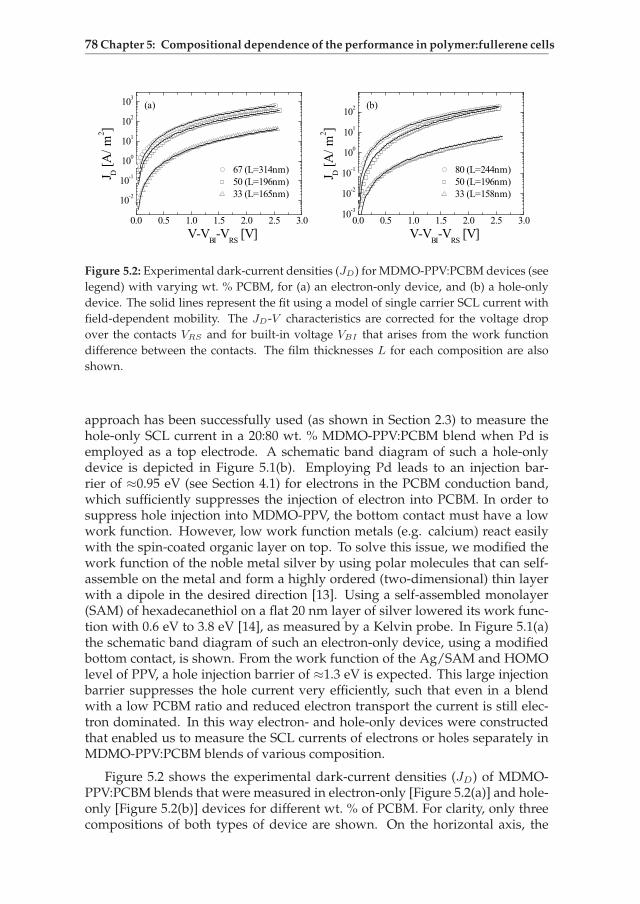
78 Chapter 5: Compositional dependence of the performance in polymer:fullerene cells
0.0 0.5 1.0 1.5 2.0 2.5 3.0
10-2
10-1
100
101
102
103
67 (L=314nm)50 (L=196nm)33 (L=165nm)
J D [A
/m2 ]
V-VBI-VRS [V]
(a)
0.0 0.5 1.0 1.5 2.0 2.5 3.010-3
10-2
10-1
100
101
102
80 (L=244nm)50 (L=196nm)33 (L=158nm)
J D [A
/m2 ]
V-VBI-VRS [V]
(b)
Figure 5.2: Experimental dark-current densities (JD) for MDMO-PPV:PCBM devices (see
legend) with varying wt. % PCBM, for (a) an electron-only device, and (b) a hole-only
device. The solid lines represent the fit using a model of single carrier SCL current with
field-dependent mobility. The JD-V characteristics are corrected for the voltage drop
over the contacts VRS and for built-in voltage VBI that arises from the work function
difference between the contacts. The film thicknesses L for each composition are also
shown.
approach has been successfully used (as shown in Section 2.3) to measure thehole-only SCL current in a 20:80 wt. % MDMO-PPV:PCBM blend when Pd isemployed as a top electrode. A schematic band diagram of such a hole-onlydevice is depicted in Figure 5.1(b). Employing Pd leads to an injection bar-rier of ≈0.95 eV (see Section 4.1) for electrons in the PCBM conduction band,which sufficiently suppresses the injection of electron into PCBM. In order tosuppress hole injection into MDMO-PPV, the bottom contact must have a lowwork function. However, low work function metals (e.g. calcium) react easilywith the spin-coated organic layer on top. To solve this issue, we modified thework function of the noble metal silver by using polar molecules that can self-assemble on the metal and form a highly ordered (two-dimensional) thin layerwith a dipole in the desired direction [13]. Using a self-assembled monolayer(SAM) of hexadecanethiol on a flat 20 nm layer of silver lowered its work func-tion with 0.6 eV to 3.8 eV [14], as measured by a Kelvin probe. In Figure 5.1(a)the schematic band diagram of such an electron-only device, using a modifiedbottom contact, is shown. From the work function of the Ag/SAM and HOMOlevel of PPV, a hole injection barrier of ≈1.3 eV is expected. This large injectionbarrier suppresses the hole current very efficiently, such that even in a blendwith a low PCBM ratio and reduced electron transport the current is still elec-tron dominated. In this way electron- and hole-only devices were constructedthat enabled us to measure the SCL currents of electrons or holes separately inMDMO-PPV:PCBM blends of various composition.
Figure 5.2 shows the experimental dark-current densities (JD) of MDMO-PPV:PCBM blends that were measured in electron-only [Figure 5.2(a)] and hole-only [Figure 5.2(b)] devices for different wt. % of PCBM. For clarity, only threecompositions of both types of device are shown. On the horizontal axis, the
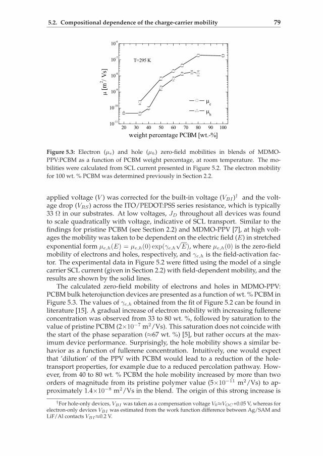
5.2. Compositional dependence of the charge-carrier mobility 79
20 30 40 50 60 70 80 90 10010-11
10-10
10-9
10-8
10-7
10-6
e
h
weight percentage PCBM [wt.-%]
[m2 /V
s]
T=295 K
Figure 5.3: Electron (µe) and hole (µh) zero-field mobilities in blends of MDMO-
PPV:PCBM as a function of PCBM weight percentage, at room temperature. The mo-
bilities were calculated from SCL current presented in Figure 5.2. The electron mobility
for 100 wt. % PCBM was determined previously in Section 2.2.
applied voltage (V ) was corrected for the built-in voltage (VBI )† and the volt-age drop (VRS) across the ITO/PEDOT:PSS series resistance, which is typically33 Ω in our substrates. At low voltages, JD throughout all devices was foundto scale quadratically with voltage, indicative of SCL transport. Similar to thefindings for pristine PCBM (see Section 2.2) and MDMO-PPV [7], at high volt-ages the mobility was taken to be dependent on the electric field (E) in stretched
exponential form µe,h(E) = µe,h(0) exp(γe,h
√E), where µe,h(0) is the zero-field
mobility of electrons and holes, respectively, and γe,h is the field-activation fac-tor. The experimental data in Figure 5.2 were fitted using the model of a singlecarrier SCL current (given in Section 2.2) with field-dependent mobility, and theresults are shown by the solid lines.
The calculated zero-field mobility of electrons and holes in MDMO-PPV:PCBM bulk heterojunction devices are presented as a function of wt. % PCBM inFigure 5.3. The values of γe,h obtained from the fit of Figure 5.2 can be found inliterature [15]. A gradual increase of electron mobility with increasing fullereneconcentration was observed from 33 to 80 wt. %, followed by saturation to thevalue of pristine PCBM (2×10⁻⁷ m2/Vs). This saturation does not coincide withthe start of the phase separation (≈67 wt. %) [5], but rather occurs at the max-imum device performance. Surprisingly, the hole mobility shows a similar be-havior as a function of fullerene concentration. Intuitively, one would expectthat ’dilution’ of the PPV with PCBM would lead to a reduction of the hole-transport properties, for example due to a reduced percolation pathway. How-ever, from 40 to 80 wt. % PCBM the hole mobility increased by more than twoorders of magnitude from its pristine polymer value (5×10⁻¹¹ m2/Vs) to ap-proximately 1.4×10⁻⁸ m2/Vs in the blend. The origin of this strong increase is
†For hole-only devices, VBI was taken as a compensation voltage V0≈VOC+0.05 V, whereas forelectron-only devices VBI was estimated from the work function difference between Ag/SAM andLiF/Al contacts VBI≈0.2 V.

80 Chapter 5: Compositional dependence of the performance in polymer:fullerene cells
not yet clear. It has been shown that films of MDMO-PPV exhibit interconnectedring-like features, due to asymmetric side chains [16]. This seems to be consis-tent with the proposition made by Pacios et al. [17] who propose that the changein film morphology upon adding PCBM molecules results in an enhanced inter-molecular interaction and, therefore, in an improved charge transfer betweenadjacent polymer chains. Based on this consideration, an enhancement in holetransport may be possible. For fullerene concentrations above 67 wt. %, the holemobility saturates. It has been pointed out by van Duren et al. that phase sepa-ration, resulting in pure PCBM domains surrounded by a homogeneous matrixof 50:50 wt. % MDMO-PPV:PCBM, sets in for concentrations above 67 wt. %PCBM [5]. As a result, the hole mobility in this homogeneous matrix of 50:50PPV:PCBM is indeed expected to saturate, as is observed experimentally in Fig-ure 5.3. Thus, a clear connection between film morphology and charge trans-port has been established. In the next section, the experimental charge-carriermobilities in MDMO-PPV:PCBM blends are applied to analyze the photocurrentgeneration and performance of solar cells based on these blends.
5.3 Device characterization under illumination
The photocurrent generation in the PPV:PCBM bulk heterojunction devices isgoverned by a number of sequential processes: the generation of excitons af-ter absorption of light by PPV, followed by exciton diffusion towards the poly-mer/fullerene (donor/acceptor) interface, and dissociation via ultrafast electrontransfer. After dissociation, a geminate pair of a hole at the donor and an elec-tron at the acceptor is formed. Due to the low dielectric constants ǫr of the or-ganic materials (ǫr typically ranges from 2-4), these e-h pairs are strongly boundby Coulomb interactions, with typical binding energies of several tenths of anelectron volt. In order to generate a photocurrent, the bound e-h pairs must dis-sociate into free charge carriers and subsequently move to the electrodes beforerecombination processes can take place.
Figure 5.4(a) shows the experimental photocurrent Jph as a function of effec-tive applied voltage (V0-V ) for three different MDMO-PPV:PCBM compositions.The photocurrent (Jph; Jph=JL-JD) is the measured current under illumination(JL) corrected for the dark current (JD), whereas the compensation voltage V0
is defined as the voltage at which the photocurrent Jph is zero. As was pre-viously demonstrated in the Section 3.1, for 20:80 wt. % MDMO-PPV:PCBMcomposition at a voltage close to the compensation voltage V0 (V0-V <0.1 V),the photocurrent increases linearly with voltage. For V0-V >0.1 V, the photocur-rent enters a regime where it is dominated by the dissociation efficiency of thebound e-h pairs, which is a field- and temperature-dependent process. Thephotocurrent of the 20:80 blend could be consistently described using a modelbased on Onsager’s theory of ion pair dissociation, in which the dissociationprobability P (E, T ) for a given electric field E and temperature T is calculated.It should be noted that the calculation of P (E, T ) requires, as input parame-ters, the lifetime of bound e-h pairs (k−1
F ), the spatial distribution of e-h pairsat the donor/acceptor interface, the dielectric constant, and the recombination
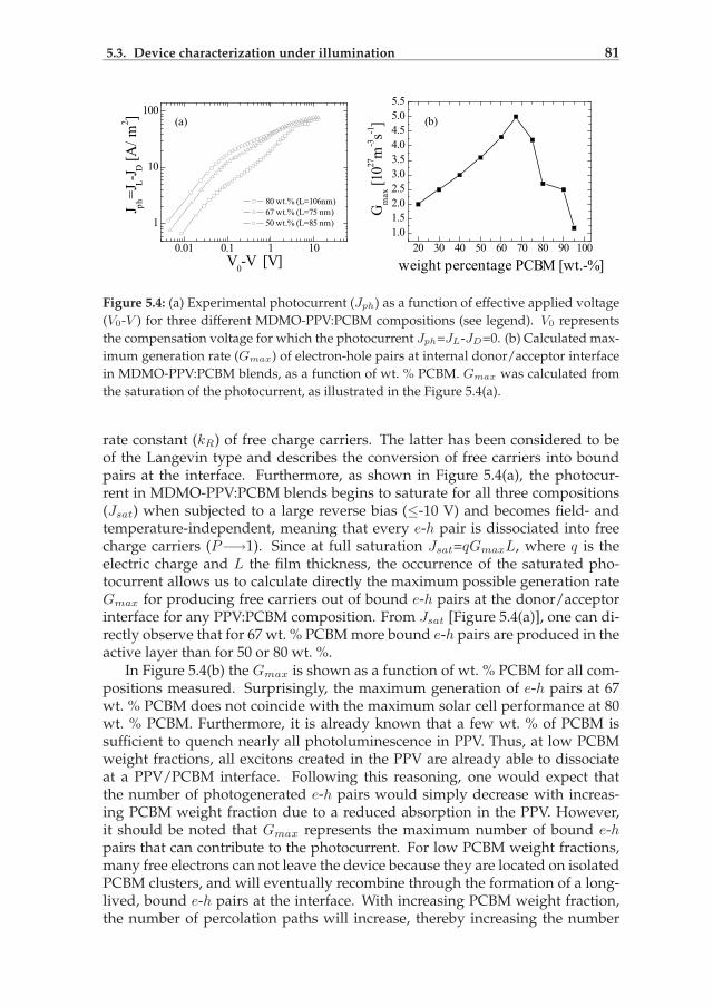
5.3. Device characterization under illumination 81
0.01 0.1 1 10
1
10
100
80 wt.% (L=106nm) 67 wt.% (L=75 nm) 50 wt.% (L=85 nm)
J ph=J
L-J D [A
/m2 ]
V0-V [V]
(a)
20 30 40 50 60 70 80 90 1001.01.52.02.53.03.54.04.55.05.5
(b)
weight percentage PCBM [wt.-%]
Gm
ax [1
027m
-3s-1
]
Figure 5.4: (a) Experimental photocurrent (Jph) as a function of effective applied voltage
(V0-V ) for three different MDMO-PPV:PCBM compositions (see legend). V0 represents
the compensation voltage for which the photocurrent Jph=JL-JD=0. (b) Calculated max-
imum generation rate (Gmax) of electron-hole pairs at internal donor/acceptor interface
in MDMO-PPV:PCBM blends, as a function of wt. % PCBM. Gmax was calculated from
the saturation of the photocurrent, as illustrated in the Figure 5.4(a).
rate constant (kR) of free charge carriers. The latter has been considered to beof the Langevin type and describes the conversion of free carriers into boundpairs at the interface. Furthermore, as shown in Figure 5.4(a), the photocur-rent in MDMO-PPV:PCBM blends begins to saturate for all three compositions(Jsat) when subjected to a large reverse bias (≤-10 V) and becomes field- andtemperature-independent, meaning that every e-h pair is dissociated into freecharge carriers (P−→1). Since at full saturation Jsat=qGmaxL, where q is theelectric charge and L the film thickness, the occurrence of the saturated pho-tocurrent allows us to calculate directly the maximum possible generation rateGmax for producing free carriers out of bound e-h pairs at the donor/acceptorinterface for any PPV:PCBM composition. From Jsat [Figure 5.4(a)], one can di-rectly observe that for 67 wt. % PCBM more bound e-h pairs are produced in theactive layer than for 50 or 80 wt. %.
In Figure 5.4(b) the Gmax is shown as a function of wt. % PCBM for all com-positions measured. Surprisingly, the maximum generation of e-h pairs at 67wt. % PCBM does not coincide with the maximum solar cell performance at 80wt. % PCBM. Furthermore, it is already known that a few wt. % of PCBM issufficient to quench nearly all photoluminescence in PPV. Thus, at low PCBMweight fractions, all excitons created in the PPV are already able to dissociateat a PPV/PCBM interface. Following this reasoning, one would expect thatthe number of photogenerated e-h pairs would simply decrease with increas-ing PCBM weight fraction due to a reduced absorption in the PPV. However,it should be noted that Gmax represents the maximum number of bound e-hpairs that can contribute to the photocurrent. For low PCBM weight fractions,many free electrons can not leave the device because they are located on isolatedPCBM clusters, and will eventually recombine through the formation of a long-lived, bound e-h pairs at the interface. With increasing PCBM weight fraction,the number of percolation paths will increase, thereby increasing the number

82 Chapter 5: Compositional dependence of the performance in polymer:fullerene cells
0.01 0.1 1 10
0.1
1
J ph/q
GmaxL
V0-V [V]
80 wt.% 50 wt.% Calculation:
80 wt.% (reference) 50 wt.% ( varied) 50 wt.% ( +< r> varied)
Figure 5.5: Experimental photocurrent (Jph) normalized to its saturation value (qGmaxL)
as a function of effective applied voltage (V0-V ) for two different MDMO-PPV:PCBM
compositions (see legend). The lines represent the calculated dissociation probability
of bound e-h pairs (P ) at the donor/acceptor interface as follows: The solid line repre-
sents the calculated P that best fits the experimental data, with 80 wt. % PCBM used as
reference. The dotted line denotes the calculated P for 50 wt. % PCBM when only the
charge-carrier mobilities 〈µ〉 have been modified; the dashed line represents the same
calculation for the case when both 〈µ〉 and the bulk dielectric constant 〈ǫr〉 are modified.
of electrons that can contribute to the photocurrent after being dissociated fromthe hole at the interface. At PCBM fractions larger than 67 wt. %, the reducedabsorption in the PPV will lead to a decrease in Gmax.
An important question remains: why do these types of devices have theiroptimum performance at 80 wt. % PCBM, despite the decrease in the numberof photogenerated bound e-h pairs? In the saturation regime V0-V >0.1 V, thephotocurrent is basically given by Jph=qGmaxP (E, T )L, in which the dissoci-ation efficiency P (E, T ) represents the field- and temperature-dependence ofthe generation rate. In order to compare P (E, T ) with experimental data, themeasured photocurrents from Figure 5.4(a) were normalized to their saturationvalue (qGmaxL), as shown in Figure 5.5 for the 50 and 80 wt. % PCBM devices.This normalized photocurrent then reflects the dissociation efficiency in the sat-uration regime for effective voltages V0-V >0.1 V. It appears that a decrease ofthe PCBM weight fraction from 80 to 50 wt. % leads to a strong reduction ofthe dissociation efficiency in the relevant voltage regime (V0-V <0.9 V). The ori-gin of this decrease in the dissociation efficiency of bound e-h pairs with de-creasing PCBM concentration will now be further addressed: For low-mobilitysemiconductors, recombination of free charge carriers is given by Langevin askR=q〈µ〉/ǫ0〈ǫr〉, where 〈ǫr〉 are the spatially averaged dielectric constants, 2.1and 3.9 for MDMO-PPV and PCBM, respectively (depending on their volumeratio), and 〈µ〉 is the effective charge-carrier mobility of electrons and holes. Theparameters in the model that vary with the PCBM fraction are kF , ǫr and kR.Since the average dielectric constant and the charge carrier mobilities are knownat each composition (Figure 5.3), kF remains the only adjustable parameter in

5.3. Device characterization under illumination 83
our calculation on changing the composition. The dissociation efficiency of thedevice with 80 wt. % PCBM (Figure 5.5, solid line) has been calculated before(see Section 3.1), and will be used as a reference. From this calculation a life-time (k−1
F ) of typically 2.5 µs was obtained, in agreement with absorption spec-troscopy measurements where bound e-h pairs in PPV:PCBM blends can stillbe detected after microseconds and even milliseconds, depending on the tem-perature [18–21]. However, these photophysical studies and quantitative mod-elling suggest a multiphasic recombination dynamics of bound e-h pairs acrossthe interface, which ranges from tens of nanoseconds to milliseconds [18–21].It is difficult to reconcile these results with the calculated k−1
F (≈2.5 µs) fromour model. We note that the experimental conditions in transient absorptionmeasurements differ strongly from the device studies. The photophysical ex-periments were performed at higher light intensity, charge density, and, mostimportantly, in the absence of an electric field. Whether these differences in ex-perimental conditions explain the apparent discrepancy is a subject of furtherinvestigation.
Next, we systematically calculated P (E, T ) for a device with 50 wt. % PCBM,changing the input parameters of the 80 wt. % device one-by-one. First, weadapted the charge-carrier mobilities and kept all other parameters constant.Figure 5.5 (dotted line) shows that the decrease in the electron and hole mobility,despite being a drop of typically an order of magnitude for an 80 to 50 wt. % de-crease in PCBM (Figure 5.3), is not solely responsible for the observed decreasein dissociation efficiency. Subsequently, besides the mobility, the change in thespatially averaged dielectric constant 〈ǫr〉, in accordance with the change in PPVand PCBM volume ratio, was also taken into account (dashed line). The calcu-lated P (E, T ) exactly fits the experimental data (Figure 5.5), without having tochange any of the other parameters. Thus, the lower separation efficiency at50 wt. % PCBM results from the combination of a decreased charge-carrier mo-bility and lower dielectric constant, resulting in a stronger e-h binding energy.This result was then used to numerically model the experimental photocurrentof a series of MDMO-PPV:PCBM blend devices with varying the PCBM com-position from 20 to 95 wt. %. Further detail on the numerical model, whichincludes P (E, T ), is given by Koster et al. [6]. The only input parameters thatchange with PCBM weight fraction are the mobilities (Figure 5.3), Gmax [Fig-ure 5.4(b)], as obtained from the fully saturated part of the photocurrent, andthe spatially averaged 〈ǫr〉. The other parameters used were identical to the fitof the 20:80 wt. % device (given in Section 3.1). Figure 5.6(a) shows the JL-Vcharacteristics under illumination of a number of composite devices with vary-ing wt. % of PCBM in MDMO-PPV, the solid lines represent the numerical fits.The excellent agreement between simulations and experiments for all compo-sitions demonstrate that the mobilities, maximum generation rate and spatiallyaveraged dielectric constant are the key parameters which govern the composi-tion dependence of the performance of MDMO-PPV:PCBM-based solar cells. Itshould be noted that, in the composition range 50 to 95 wt. %, all calculationswere done with a constant lifetime k−1
F of 2.5 µs, whereas, for 40 wt. %, a lifetimeof 40 µs had to be used to fit the experimental data. At even lower fractions, thelifetime further increases. The exact origin of this increase in the lifetime for low

84 Chapter 5: Compositional dependence of the performance in polymer:fullerene cells
-0.4 -0.2 0.0 0.2 0.4 0.6 0.8 1.0
-30
-20
-10
0
10
20 95 wt.%80 wt.%67 wt.%40 wt.%
J L [A/m
2 ]
V [V]
(a)2025303540455055606570
20 30 40 50 60 70 80 90 100
0.0
0.2
0.4
0.6
0.8
1.0
FF [%
]
FF
(b)
weight percentage PCBM [wt.-%]
/m
ax
Figure 5.6: (a) JL-V curves under illumination of the ITO/PEDOT:PSS/
MDMO-PPV:PCBM/LiF/Al devices with varying wt. % PCBM in MDMO-PPV.
The devices were illuminated using a tungsten-halogen lamp with a power intensity
of 180 mW/cm2. The solid lines represent the numerical calculation using a model
by Koster et al. [6]. (b) Experimental power conversion efficiency η normalized to the
maximum value and fill factor (FF) (see legend) with varying PCBM composition, at
room temperature. The solid lines represent the numerical calculations.
PCBM fractions is not yet clear, but its onset corresponds to the measured dropin the hole transport. Whether the low mobility, which might hinder the holesto reach the donor/acceptor interface, is responsible for this lifetime increase isa subject of further study.
From the excellent agreement between simulated and experimental pho-tocurrent [Figure 5.6(a)], it directly follows that the model also accurately de-scribes the experimental power conversion efficiency η (normalized to its maxi-mum value ηmax) and the fill factor (FF) as a function of wt. % PCBM, as shownin Figure 5.6(b). Since the open-circuit voltage (VOC) of these blends is merelyrelated to the electronic levels of the donor and acceptor and the type of contactsused (as discussed in Section 4.1), the variation in η is mainly due to a change inthe short-circuit current (JSC) and/or FF. For PCBM concentrations exceeding80 wt. %, the decrease in optical density of the film due to the poorer absorptionof the PCBM compared to the MDMO-PPV, combined with a reduced interfacearea between donor and acceptor, results in a drop of the maximum generationrate Gmax of e-h pairs. This will give rise to a decrease in JSC and consequentlyη, despite the efficient charge separation and high FF. For example, the decreaseby a factor of 2.3 in η [Figure 5.6(b)] between 80 and 95 wt. % is entirely due tothe decrease in Gmax [Figure 5.4(b)].
The most interesting range for the device performance is from 80 to 67 wt. %,where phase separation starts to develop. In this range, a drop in device effi-ciency by 40% was measured, despite an increased Gmax. Recently, we demon-strated that at short-circuit (SC) conditions in 20:80 wt. % MDMO-PPV:PCBMblends, only 60% of the total e-h pairs that are generated at donor/acceptorinterface, after photoinduced electron transfer, are separated into free chargecarriers and subsequently collected at the electrodes (see Section 3.1), which isone of the important loss mechanisms in this material system. Figure 5.7 shows

5.4. Conclusion 85
20 30 40 50 60 70 80 90 1000
10
20
30
40
50
60
70
weight percentage PCBM [wt.-%]
sc [%
]
Figure 5.7: Calculated charge separation efficiency at short-circuit condition (ηsc) as a
function of weight percentage PCBM.
the calculated separation efficiency of e-h pairs at SC (ηsc) for all fitted MDMO-PPV:PCBM compositions. ηsc strongly decreases for fullerene concentrationsbelow 80 wt. %, resulting from the lower charge-carrier mobilities and lowerdielectric constant (see Figure 5.5). As a result, the benefit of a higher Gmax
at 67 wt. % is completely compensated by a poorer ηsc: it is only 36.8% at 67wt. % PCBM (Figure 5.7). Below 67 wt. %, the Gmax gradually decreases and,strengthened by a strong decrease in hole transport, the separation efficiency ofbound e-h pairs is further reduced, which is detrimental for the device perfor-mance. As a consequence, the loss in the device performance below 67 wt. %is due to a combined effect of a reduced Gmax, weaker separation efficiency ofbound e-h pairs from the donor/acceptor interface, and a strong decrease in thehole transport.
Consequently, the most important factor for obtaining power efficiencies of2.5% presently reported for the MDMO-PPV:PCBM blends is the enhancementof µh in the blend by more than two orders of magnitude, as compared to thepristine MDMO-PPV. Without such an enhancement, these efficiencies wouldnot be possible in this material system, and the performance would be stronglylimited by space-charge effects (see Section 3.2). The optimum performance at80 wt. % PCBM is governed by the best compromise between absorption (Gmax),dissociation (〈ǫr〉), and charge transport (µh).
5.4 Conclusion
The electron and hole mobilities have been independently measured in MDMO-PPV: PCBM blend films with varying PCBM concentration. The electron mobil-ity in the PCBM phase gradually increases with increasing fullerene concen-tration, up to 80 wt. %, due to an increasing number of continuous percolatedpathways from the bottom to the top electrode. Surprisingly, the hole mobilityin MDMO-PPV shows similar behavior as a function of fullerene concentration:from 40 wt. %, it starts to increase from that of the pristine MDMO-PPV hole mo-

86 Chapter 5: Compositional dependence of the performance in polymer:fullerene cells
bility and saturates beyond 67 wt. %, at a value which is more than two ordersof magnitude higher. This enhancement and its saturation are strongly relatedto recent findings on the morphology of these devices.
The resulting electron and hole mobilities were used to study the photocur-rent generation of MDMO-PPV:PCBM bulk heterojunction solar cells. Using afull numerical model to fit the experimental data, it is shown that, for PCBMconcentrations of more than 80 wt. %, the reduced light absorption and inter-face area between donor and acceptor is responsible for the poor device perfor-mance. From 80 to 67 wt. %, the decrease in power conversion efficiency, despitean increase in the maximum generation rate of e-h pairs at donor/acceptor in-terface, is due to the decrease in separation efficiency of bound e-h pairs fromthe donor/acceptor interface. Finally, below 67 wt. %, the reduced generationrate and strong decrease in the hole transport further diminish the performanceof this kind of solar cells.
5.5 Experimental section
Device Preparation: All solar cell devices used to investigate the photocur-rent in this study were prepared using indium-tin-oxide (ITO) coated glasssubstrates. To supplement this bottom electrode, a hole-transport layer of PE-DOT:PSS (Baytron P VP Al 4083) was spin-coated from an aqueous dispersionsolution, under ambient conditions, before drying the substrates at 140 oC. Next,composite layers of MDMO-PPV and PCBM were spin-coated from chloroben-zene solution on top of the PEDOT:PSS layer, with film thicknesses ranging from75 to 130 nm. To complete the solar cell devices, 1 nm lithium fluoride (LiF)topped with aluminum (Al, 110 nm) electrodes was deposited by thermal evap-oration under vacuum (1×10⁻⁷ mbar; 1 mbar=100 Pa).Device Characterization: The current density versus voltage curves were mea-sured in N2 atmosphere (<1 ppm O2 and <1 ppm H2O) at room temperaturewith a computer-controlled Keithley 2400 Source Meter. To measure the pho-tocurrent (JL), the devices were illuminated at the transparent ITO electrode bywhite light tungsten-halogen lamp with an intensity of 180 mW/cm2. The lamplight output was filtered by a Schott KG1 and GG385 filter resulting in a spectralrange of 400-900 nm with its maximum at 650 nm. Light power was measuredwith an Ophir Laser Power Meter set at 610 nm. Energetically, the devices areapproximated by the metal-insulator-metal picture, with the LUMO of the ac-ceptor (PCBM) and the HOMO of the donor (MDMO-PPV) as conduction andvalence band, respectively.

REFERENCES 87
References
[1] S. E. Shaheen, C. J. Brabec, N. S. Sariciftci, F. Padinger, T. Fromherz, J. C. Hummelen,2.5% efficient organic plastic solar cells, Applied Physics Letters 78 (2001), 841.
[2] A. Aharony, D. Stauffer, Introduction to percolation theory, 2nd ed., Taylor and Francis,London (1993).
[3] M. Sahimi, Applications of percolation theory, Taylor and Francis, London (1994).
[4] S. Hotta, S. D. D. V. Rughooputh, A. J. Heeger, Conducting polymer composites of solu-ble polythiophenes in polystyrene, Synthetic Metals 22 (1987), 79.
[5] J. K. J. van Duren, X. N. Yang, J. Loos, C. W. T. Bulle-Lieuwma, A. B. Sieval,J. C. Hummelen, R. A. J. Janssen, Relating the morphology of poly(p-phenylene viny-lene)/methanofullerene blends to solar-cell performance, Advanced Functional Materials14 (2004), 425.
[6] L. J. A. Koster, E. C. P. Smits, V. D. Mihailetchi, P. W. M. Blom, Device model forthe operation of polymer/fullerene bulk heterojunction solar cells, Physical Review B, 72(2005), 085205.
[7] P. W. M. Blom, M. J. M. deJong, M. G. vanMunster, Electric-field and temperature de-pendence of the hole mobility in poly(p-phenylene vinylene), Physical Review B 55 (1997),R656.
[8] S. A. Choulis, J. Nelson, Y. Kim, D. Poplavskyy, T. Kreouzis, J. R. Durrant, D. D. C.Bradley, Investigation of transport properties in polymer/fullerene blends using time-of-flight photocurrent measurements, Applied Physics Letters 83 (2003), 3812.
[9] R. Pacios, J. Nelson, D. D. C. Bradley, C. J. Brabec, Composition dependence of electronand hole transport in polyfluorene: [6,6]-phenyl c-61-butyric acid methyl ester blend films,Applied Physics Letters 83 (2003), 4764.
[10] W. Geens, S. E. Shaheen, C. J. Brabec, J. Poortmans, N. S. Sariciftci, Electronic proper-ties of novel materials - Molecular nanostructures, Euroconf.(Eds: H. Kuzmany, J. Fink,M. Mehring, S. Roth), American Institute of Physics, Melville, NY (2000), p. 516.
[11] J. F. Nierengarten, T. Gu, T. Aernouts, W. Geens, J. Poortmans, G. Hadziioan-nou, D. Tsamouras, Fullerene-oligophenyleneethynylene conjugates: relationships be-tween charge-carrier mobility, photovoltaic characteristics and chemical structure, AppliedPhysics A-Materials Science & Processing 79 (2004), 47.
[12] C. Tanase, E. J. Meijer, P. W. M. Blom, D. M. de Leeuw, Unification of the hole transportin polymeric field-effect transistors and light-emitting diodes, Physical Review Letters 91(2003), 216601.
[13] I. H. Campbell, S. Rubin, T. A. Zawodzinski, J. D. Kress, R. L. Martin, D. L. Smith,N. N. Barashkov, J. P. Ferraris, Controlling schottky energy barriers in organic electronicdevices using self-assembled monolayers, Physical Review B 54 (1996), 14321.
[14] B. de Boer, A. Hadipour, M. M. Mandoc, T. van Woudenbergh, P. W. M. Blom, Tuningof metal work functions with self-assembled monolayers, Advanced Materials 17 (2005),621.
[15] V. D. Mihailetchi, B. de Boer, C. Melzer, L. J. A. Koster, P. W. M. Blom, Electron andhole transport in poly(para-phenylene vinylene):methanofullerene bulk heterojunction solarcells, Proccedings of SPIE 5520 (2004), 20.
[16] M. Kemerink, J. K. J. van Duren, P. Jonkheijm, W. F. Pasveer, P. M. Koenraad, R. A. J.

88 Chapter 5: Compositional dependence of the performance in polymer:fullerene cells
Janssen, H. W. M. Salemink, J. H. Wolter, Relating substitution to single-chain confor-mation and aggregation in poly(p-phenylene vinylene) films, Nano Letters 3 (2003), 1191.
[17] R. Pacios, D. D. C. Bradley, J. Nelson, C. J. Brabec, Efficient polyfluorene based solarcells, Synthetic Metals 137 (2003), 1469.
[18] T. Offermans, S. C. J. Meskers, R. A. J. Janssen, Charge recombination in a poly(para-phenylene vinylene)-fullerene derivative composite film studied by transient, nonresonant,hole-burning spectroscopy, Journal of Chemical Physics 119 (2003), 10924.
[19] I. Montanari, A. F. Nogueira, J. Nelson, J. R. Durrant, C. Winder, M. A. Loi, N. S.Sariciftci, C. Brabec, Transient optical studies of charge recombination dynamics in a poly-mer/fullerene composite at room temperature, Applied Physics Letters 81 (2002), 3001.
[20] J. Nelson, Diffusion-limited recombination in polymer-fullerene blends and its influence onphotocurrent collection, Physical Review B 67 (2003), 155209.
[21] T. J. Savenije, J. E. Kroeze, M. M. Wienk, J. M. Kroon, J. M. Warman, Mobility anddecay kinetics of charge carriers in photoexcited pcbm/ppv blends, Physical Review B 69(2004), 155205.
6Exploring poly(3-hexylthiophene):fullerene
solar cells∗
Abstract
In the search for new materials that can overcome the problem of poor charge-carrier transport, absorption, and environmental stability, a new class of con-jugated polymers, such as polythiophenes, are currently being used in or-ganic bulk heterojunction solar cells. Composites of regioregular poly(3-hexyl-thiophene) (P3HT) and a fullerene derivative (PCBM) have demonstrated anincrease of the photovoltaic efficiency upon thermal annealing of the devices, asfollows from measurements of the external quantum efficiency and the current-voltage characteristics. In this chapter, the effect of controlled thermal anneal-ing on charge transport and photogeneration in P3HT:PCBM bulk heterojunc-tion solar cells have been investigated. With respect to the charge transport, itis demonstrated that the electron mobility dominates the transport of the cell,varying from 10−8 m2/Vs in as-cast devices to ≈3×10⁻⁷ m2/Vs after thermalannealing. The hole mobility in the P3HT phase of the blend is dramatically af-fected by thermal annealing. It increases more than three orders of magnitude,to reach a value up to ≈2×10⁻⁸ m2/Vs after the annealing process, as a resultof an improved crystallinity of the film. Moreover, upon annealing the absorp-tion spectrum of P3HT:PCBM blends undergoes a strong red-shift, improvingthe spectral overlap with the solar emission, which result in an increase of morethan 60% in the generation rate of charge carriers. Subsequently, the experimen-tal electron and hole mobilities were used to study the photocurrent generationin P3HT:PCBM devices as a function of thermal annealing temperature. The re-sults indicates that the most important factor leading to a strong enhancementof the efficiency, compared with non-annealed devices, is the increase of the holemobility in the P3HT phase of the blend.
∗The main results of this chapter are in press as: V. D. Mihailetchi, H. X. Xie, B. de Boer, L. J. A.Koster, P. W. M. Blom, Advanced Functional Materials.
89

90 Chapter 6: Exploring poly(3-hexylthiophene):fullerene solar cells
6.1 Introduction
Most of the previous work on the physics of bulk heterojunction (BHJ) solarcells was performed on blends of MDMO-PPV and soluble fullerene derivativesas PCBM. The power conversion efficiencies (η) reported for this type of de-vices, measured under AM1.5 standard test conditions [1], range from 2.5-3%[2, 3]. However, to achieve these efficiencies, up to 80 wt.% PCBM, a materialwhich hardly contributes to the absorption, has to be added into the MDMO-PPV:PCBM mixture [2–5]. In Chapter 5, it is demonstrated that one of the mainreasons for this relatively large amount of PCBM is the enhancement of thehole transport in MDMO-PPV, which is the slowest carrier, when blended withPCBM [5]. Furthermore, a too low hole mobility will also lead to the build-up ofspace-charge in the solar cell, as previously shown in Section 3.2, which is detri-mental for the fill factor and efficiency [6]. Therefore, an intrinsically higherhole mobility in the blend permits to reduce the amount of PCBM and inhibitsthe occurrence of space-charge, which will further increase the magnitude of thephotogenerated current (Jph) and enhance the η.
Among the materials investigated so far, regioregular poly(3-hexylthiophene)(P3HT) has demonstrated promising physical properties such as environmentalstability, reasonably high hole mobility and an improved absorption as com-pared with PPV based devices. Thermal annealing of the P3HT:PCBM blenddevices dramatically improves the external quantum efficiency and η of thesecells [7–10]. It is well known that an enhanced degree of crystallinity can be in-duced in polythiophene films by thermal annealing. This controlled crystalliza-tion and orientation of polythiophene polymer chains can significantly improvethe hole mobility. After annealing, energy conversion efficiency as high as 3.5%has been reported [9, 10]. Besides this, a red shift of the optical absorption ofP3HT inside the blend is observed [7], providing an improved overlap with thesolar emission.
Figure 6.1 shows the experimental Jph of such P3HT:PCBM blends (50:50wt. %) in a double logarithm plot as a function of effective applied voltage (V0-V )§. The curves correspond to the different postproduction treatment as fol-low: as-cast, thermally annealed at a temperature where the enhancement in ηis maximized (120 oC), and annealed at a lower temperature (70 oC). Thermalannealing was performed on complete devices, i.e., with the photoactive layerbetween the electrodes, on the hot plate for a period of 4 minutes. It appearsfrom Figure 6.1 that the photocurrent shows a strong enhancement after ther-mal annealing. For the completely annealed device (at 120 oC), the short-circuitcurrent (JSC) increases by a factor of 5, the fill factor (FF) by a factor of 2 and theoverall enhancement of η is about one order of magnitude when compared withthe device as-cast. This dramatic boost in the efficiency as a result of thermaltreatment of the photoactive layer has been suggested to be caused by burningof shunts [9], increase in hole mobility due to crystallization of the polymer, a
§The photocurrent (Jph; Jph=JL-JD) is the measured current under illumination (JL) correctedfor the dark current (JD), whereas V0 is the compensation voltage. V0 is defined as the voltageat which Jph is zero: VOC<V0≤VOC+0.048 V for all the experiments presented throughout thischapter.
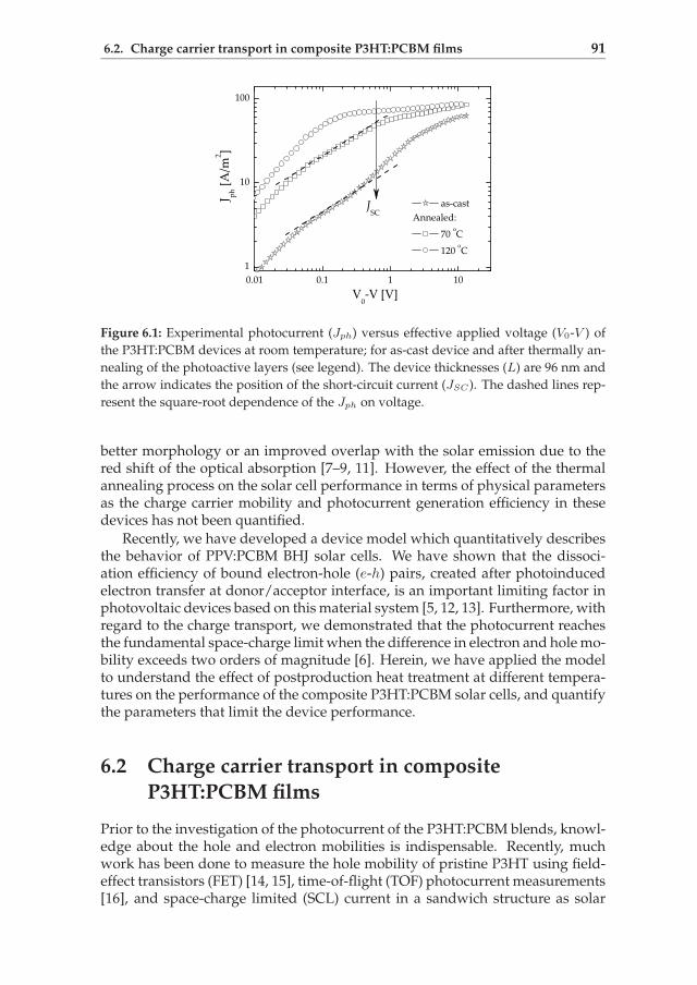
6.2. Charge carrier transport in composite P3HT:PCBM films 91
0.01 0.1 1 101
10
100
as-castAnnealed:
70 oC
120 oC
J ph [A
/m2 ]
V0-V [V]
JSC
Figure 6.1: Experimental photocurrent (Jph) versus effective applied voltage (V0-V ) of
the P3HT:PCBM devices at room temperature; for as-cast device and after thermally an-
nealing of the photoactive layers (see legend). The device thicknesses (L) are 96 nm and
the arrow indicates the position of the short-circuit current (JSC ). The dashed lines rep-
resent the square-root dependence of the Jph on voltage.
better morphology or an improved overlap with the solar emission due to thered shift of the optical absorption [7–9, 11]. However, the effect of the thermalannealing process on the solar cell performance in terms of physical parametersas the charge carrier mobility and photocurrent generation efficiency in thesedevices has not been quantified.
Recently, we have developed a device model which quantitatively describesthe behavior of PPV:PCBM BHJ solar cells. We have shown that the dissoci-ation efficiency of bound electron-hole (e-h) pairs, created after photoinducedelectron transfer at donor/acceptor interface, is an important limiting factor inphotovoltaic devices based on this material system [5, 12, 13]. Furthermore, withregard to the charge transport, we demonstrated that the photocurrent reachesthe fundamental space-charge limit when the difference in electron and hole mo-bility exceeds two orders of magnitude [6]. Herein, we have applied the modelto understand the effect of postproduction heat treatment at different tempera-tures on the performance of the composite P3HT:PCBM solar cells, and quantifythe parameters that limit the device performance.
6.2 Charge carrier transport in composite
P3HT:PCBM films
Prior to the investigation of the photocurrent of the P3HT:PCBM blends, knowl-edge about the hole and electron mobilities is indispensable. Recently, muchwork has been done to measure the hole mobility of pristine P3HT using field-effect transistors (FET) [14, 15], time-of-flight (TOF) photocurrent measurements[16], and space-charge limited (SCL) current in a sandwich structure as solar

92 Chapter 6: Exploring poly(3-hexylthiophene):fullerene solar cells
cells or light-emitting diode configuration [17, 18]. The measured hole mobil-ity ranges from 10−8 m2/Vs in TOF and SCL current, up to 10−5 m2/Vs in aFET. It should be noted that regioregular P3HT self-organizes into crystallinestructure and due to the π-π stacking direction the charge (hole) transport is ex-tremely efficient. Since in FET measurements the current travels in the plane ofthe film (parallel to the substrate), the anisotropy in the polymer chain orienta-tion strongly contributes to the difference in the measured mobility. Moreover,a different molecular-weight of P3HT, the presence of PCBM and/or applyingof a thermal treatment will also affect the measured electron and hole mobili-ties [15, 17]. Therefore, the relevant values for charge carrier mobilities can onlybe obtained when measured in the same configuration and experimental condi-tions as used in an operational solar cell device.
In Chapter 5, it is shown that electron and hole mobilities in the blend canbe determined from current-voltage measurements by using suitable electrodeswhich either suppress the injection of electrons or holes, resulting in a hole- orelectron-only device, respectively [5]. In this section, we have applied this tech-nique to measure either the hole or electron current in blends of P3HT:PCBMas a function of the thermal annealing temperature of the spin-coated films. Tofabricate the hole-only devices palladium was evaporated as a top electrode onan indium tin oxide (ITO)/PEDOT:PSS/P3HT:PCBM structure. The work func-tion of PEDOT:PSS matches the HOMO of P3HT at 4.9 eV, forming an Ohmiccontact for hole injection [8, 17], whereas palladium strongly suppresses elec-tron injection into PCBM due to the large mismatch between its work functionand LUMO level of PCBM [19]. A schematic diagram of a hole-only device isshown in Chapter 5 [Figure 5.1(b)]. In order to suppress the hole injection into
0.0 0.5 1.0 1.5 2.0 2.5 3.010
-4
10-3
10-2
10-1
100
101
102
103
J D [
A/
m2 ]
V-VBI
-VRS
[V]
(a)
0.0 0.5 1.0 1.5 2.0 2.5 3.0
10-1
100
101
102
103
104
J D [
A/
m2 ]
V-VBI
-VRS
[V]
(b)
Figure 6.2: Experimental dark current densities (JD) of the 50:50 wt. % P3HT:PCBM
blend devices, measured at room temperature in the hole-only (a) and electron-only (b)
devices configuration. The symbols correspond to different thermal annealing tempera-
ture of the photoactive layer as follow: as-cast (), 90 oC (), and 120 oC (©), respec-
tively. Here, the thickness of the annealed hole-only devices (,©) is 120 nm, whereas
for the other devices is 220 nm. The solid lines represent the fit using a model of single
carrier SCL current with field-dependent mobility. The JD-V characteristics are corrected
for the voltage drop over the contacts VRS and the built-in voltage VBI that arises from
the work function difference between the contacts.
6.2. Charge carrier transport in composite P3HT:PCBM films 93
P3HT, the bottom contact must have a low work function. Recently, we havedemonstrated that the work function of a noble metal (as silver) can be modifiedusing a self-assembled monolayer (SAM) [20]. This technique works very welland successful electron-only devices were constructed using blends of MDMO-PPV:PCBM (see Chapter 5). Therefore, similar electron-only devices were alsoconstructed for the P3HT:PCBM blends, the schematic band diagram of such anelectron-only device is presented as inset in Figure 5.1(a).
Figure 6.2 shows the experimental dark current densities (JD) of P3HT:PCBMblends that were measured in hole-only [Figure 6.2(a)] and electron-only [Fig-ure 6.2(b)] devices for different thermal annealing temperature performed onthe completed device. For clarity, only the devices that were measured as-cast,after thermal annealing at 90 oC and 120 oC, are shown. The applied voltagewas corrected for the built-in voltage (VBI ) and the voltage drop (VRS) due tothe substrate’s series resistance∗. When the applied voltage is greater that VBI ,JD throughout all devices scales quadratically with voltage, indicative of space-charge limited transport. This observation is common for low mobility disor-dered semiconductors and it allows for a direct determination of the mobility[5, 17]. The experimental data in Figure 6.2 were fitted using the model of asingle-carrier SCL current (see Section 2.2) with field-dependent mobility given
by µe,h(E) = µe,h(0) exp(γe,h
√E), where µe,h(0) is the zero-field mobility of
electrons and holes, respectively, and γe,h is the field-activation factor. The re-sults of the calculations are shown by the solid lines in Figure 6.2.
Figure 6.3 shows the calculated zero-field mobility of electrons and holes in50:50 wt. % blends of P3HT:PCBM devices as a function of the annealing tem-perature. For comparison, the hole mobility of pristine P3HT, measured underthe same experimental conditions, is also shown. It appears from Figure 6.3 thatthe hole mobility in pristine P3HT is hardly affected by thermal annealing, witha typical value of (1.4-3.0)×10−8 m2/Vs. This mobility was found to be com-pletely field independent (γh=0) and fully consistent with previously reportedvalues for high molecular-weight P3HT (as the one used here) [17]. In contrast,the hole mobility of P3HT in the blend is strongly affected by the presence ofPCBM and it drops almost 4 orders of magnitude for an as-cast device. Uponannealing, however, the mobility starts to increase sharply with an onset at 50-60oC, followed by saturation to approximately the value of the pristine polymerwhen the devices are annealed above 120 oC. Also, the field activation factorgradually decreases from γh=4.0×10⁻⁴ (V/m)−1/2 for the as-cast film to γh=0for the devices annealed above 90 oC. Moreover, the electron mobility of PCBMin the blend is also affected by thermal annealing: For as-cast films the electronmobility is (1-2)×10−8 m2/Vs, being typically a factor of 5000 higher than thehole mobility. As a result, the charge transport in as-cast films is strongly unbal-anced and the current is fully dominated by the electrons. Interestingly, for thesame volume fraction the electron mobility in as-cast P3HT:PCBM films resem-
∗For hole-only devices VBI (VBI ≈0.2 V) was estimated from the difference between the workfunction of Pd and HOMO level of P3HT, whereas for electron-only devices VBI was estimatedfrom the work function difference between Ag/SAM and LiF/Al contacts VBI≈0.2 V. The seriesresistance was determined from the reference devices fabricated without the photoactive layer andwas found to be 4-5 Ω for electron-only devices, and 25-35 Ω for hole-only devices.

94 Chapter 6: Exploring poly(3-hexylthiophene):fullerene solar cells
20 40 60 80 100 120 140 16010
-12
10-11
10-10
10-9
10-8
10-7
10-6
pristine P3HT
holesP3HT:PCBM
electrons holes
as cast
µ [m
2 /V
s]
Annealing Temperature [oC]
Figure 6.3: Room temperature electron (•) and hole () zero-field mobilities in 50:50 wt. %
blends of P3HT:PCBM as a function of postproduction annealing temperature of the com-
pleted devices. For comparison, the hole mobility measured in pristine P3HT devices ()
is also shown. The mobilities were calculated from the SCL current measured using the
electron- and hole-only device configuration (Figure 6.2).
bles the value measured previously in MDMO-PPV:PCBM blends (see Chapter5). However, thermal annealing of P3HT:PCBM films results in an enhancedelectron mobility by typically a factor of 30, with an onset corresponding to thesame temperature observed for the hole mobility, as inferred from Figure 6.3.
Furthermore, modulated Differential Scanning Calorimetry (DSC) has beenused to assess the degree of crystallinity of the particular batch of regioregu-lar P3HT used in these experiments. The DSC thermogram, measured with ascan rate of 2 K/minute, reveals two weak changes in the gradient at ≈50 oCwhich correspond to the onset of the side-chain melting temperature (Tsc), andat ≈125 oC corresponding to the onset of the glass transition temperature (Tg);Furthermore, a strong melting peak appears at ≈215 oC. These results are valu-able for understanding the film forming mechanism and the charge transportin these blends. It has been shown that regioregular P3HT self-organizes intomicrocrystalline lamellae structure, forming well-defined whiskerlike entities[21–23]. This predominantly crystalline film may already have been formed inthe pristine P3HT directly after the spin-coating process and thermal annealingdoes not further improve the crystallinity. As a consequence, the hole mobilityin the pristine P3HT is not expected to change after the annealing treatment ofthe film. However, in the blend devices, the presence of PCBM molecules mightprevent immediate crystallization of P3HT after the spin coating process, re-sulting in a more amorphous film. This is strengthened by a recent prepositionmade by Yang et al. who argue that a rather homogeneous nanoscale distribu-tion of PCBM in the P3HT matrix is present in the film as cast [11]. Consequently,the conformation of the P3HT chains and the way they pack together result in aweak interchain interaction which strongly suppresses the hole mobility. Uponthermal annealing, slow crystallization of P3HT takes place and demixing be-tween P3HT and PCBM is observed [11], which leads to an enhanced charge
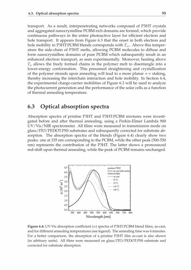
6.3. Optical absorption spectra 95
transport. As a result, interpenetrating networks composed of P3HT crystalsand aggregated nanocrystalline PCBM-rich domains are formed, which providecontinuous pathways in the entire photoactive layer for efficient electron andhole transport. It appears from Figure 6.3 that the onset in both electron andhole mobility in P3HT:PCBM blends corresponds with Tsc. Above this temper-ature the side-chain of P3HT melts, allowing PCBM molecules to diffuse andform nanocrystalline domains of pure PCBM which subsequently result in anenhanced electron transport, as seen experimentally. Moreover, heating aboveTg allows the freely formed chains in the polymer melt to disentangle into alower-energy conformation. This presumed straightening and crystallizationof the polymer strands upon annealing will lead to a more planar π-π staking,thereby increasing the interchain interaction and hole mobility. In Section 6.4,the experimental charge-carrier mobilities of Figure 6.3 will be used to analyzethe photocurrent generation and the performance of the solar cells as a functionof thermal annealing temperature.
6.3 Optical absorption spectra
Absorption spectra of pristine P3HT and P3HT:PCBM mixtures were investi-gated before and after thermal annealing, using a Perkin-Elmer Lambda 900UV/Vis/NIR spectrometer. All films were measured in transmission mode onglass/ITO/PEDOT:PSS substrates and subsequently corrected for substrate ab-sorption. The absorption spectra of the blends (Figure 6.4) clearly show twopeaks: one at 335 nm corresponding to the PCBM, while the other peak (500-550nm) represents the contribution of the P3HT. The latter shows a pronouncedred-shift upon thermal annealing, while the peak of PCBM remains unchanged.
350 400 450 500 550 600 650 700 750 8000.0
0.5
1.0
1.5
2.0
2.5
3.0
3.5
4.0
4.5 pristine P3HT as-cast [arb.units]
P3HT:PCBM as cast
53 oC
70 oC
110 oC
150 oC
α [1
06 m-1]
Wavelength [nm]
Figure 6.4: UV-Vis absorption coefficient (α) spectra of P3HT:PCBM blend films, as-cast,
and for different annealing temperatures (see legend). The annealing time was 4 minutes.
For a better comparison, the absorption of a pristine P3HT film as-cast is also shown
(in arbitrary units). All films were measured on glass/ITO/PEDOT:PSS substrate and
corrected for substrate absorption.

96 Chapter 6: Exploring poly(3-hexylthiophene):fullerene solar cells
Similar results have been reported by other authors [7, 24]. Furthermore, themobility measurements presented in Figure 6.3, correlated with the morphol-ogy investigations [11, 21–23] pointed out that there is a change in the physicalconformation of the P3HT chains. As a result, the packing of P3HT together inthe presence of PCBM relative to pristine P3HT films changes, thereby adaptingthe relevant optical and electronic properties that are critical for the operationof these devices. This change in the conformation is also reflected in the ab-sorption spectra of the blend films. As shown in Figure 6.4, the UV-Vis absorp-tion coefficient spectra of the blend film as-cast is strongly blue shifted with re-spect to the spectrum of pristine P3HT. This shift might originate from a tighterchain coil, produced by twisting the polymer backbone or broken conjugation inthe presence of PCBM, resulting in segments with a shorter conjugation lengthand weaker interchain interaction. This is in agreement with absorption spec-tra of pristine P3HT, which show no change after annealing, but rather a smallincrease in the absorption intensity (not shown). Upon annealing, the PCBMdemixes from the P3HT, as inferred by Yang et al. [11], thereby increasing thedegree of crystallinity of the polymer and consequently undergoes a noticeableshift to the red, approaching the spectrum of the pristine polymer. It appearsfrom Figure 6.4 that the shift of the optical absorption is maximized when thedevices are annealed above 100 oC, which closely corresponds with the temper-ature at which the hole mobility in the blend begins to approach that of pristinepolymer.
Nevertheless, the net effect of the red-shift of the optical absorption uponannealing, with respect to the non-treated film, is that it will improve the spec-tral overlap with solar emission, resulting in an increased absorption in the de-vice. The absorption coefficients (α), shown in Figure 6.4, can be used to esti-mate the amount of additionally absorbed photons upon thermally annealingthe P3HT:PCBM BHJ solar cell. The calculation was done using the following
400 500 600 700 8000.0
0.2
0.4
0.6
0.8
1.0
Wavelength [nm]
Light SourceP3HT:PCBM
as-castAnnealed:
120 oC
Cou
nts
[ar
b. u
nit
s]
Figure 6.5: Fraction of absorbed photons (Iabs) from the excitation source (I0) by a
P3HT:PCBM solar cell with a thickness L=96 nm. The calculation is done for the film
as-cast and annealed at 120 oC (see legend) using the absorption coefficients (α) given in
the Figure 6.4.

6.4. Device characterization under illumination 97
equation:
Iabs(λ) = I0(λ)[(
1 − 10−α(λ)L)
+ R(λ)10−2α(λ)L(
10α(λ)L − 1)]
, (6.1)
where Iabs is the fraction of absorbed photons, I0 the light source spectrum andR is the reflectivity of the top electrode material (Al; R≈92% on the involvedspectral range) [25]. The results of the calculations are shown in the Figure 6.5together with the light source spectrum used in our measurements (I0), for adevice with thickness (L) of 96 nm. After integrating the area under the curvesit appears that the annealed device improves light harvesting by approximately60% relative to the non-treated device. In the next section this information willbe used to explain the enhanced photocurrent generation in the annealed de-vices.
6.4 Device characterization under illumination
6.4.1 The effect of thermal annealing on solar cell performance
After the investigation of the charge transport and optical absorption spec-troscopy we proceed with the analysis of the solar cell performance upon ther-mal annealing of the photoactive P3HT:PCBM layer. The devices consist of 50:50wt. % P3HT:PCBM blends which were spin-coated from a single chloroform so-lution on an ITO/PEDOT:PSS substrate, followed by the evaporation of a thinsamarium (8 nm)/aluminum (100 nm) top electrode. The annealing was per-formed after completing the devices in N2 atmosphere on a hot plate for du-ration of 4 minutes. The active layer thickness ranges from 94 to 97 nm for allfabricated devices.
Figure 6.6 shows the variation of the principal photovoltaic parameters (i.e.their mean values together with the standard deviations) as a function of anneal-ing temperature. The devices were illuminated from a halogen lamp with thespectral range and shape shown in Figure 6.5, calibrated using a silicon diodeat an intensity of approximately 1.15 Sun (115 mW/cm2). The VOC is relativelyconstant and varies less than 40 mV, showing a slight increase above 150 oC an-nealing temperature. Conversely, all remaining device parameters show a veryfast increase with annealing temperature between 50 and 110 oC, followed bysaturation. The onset of this enhancement strongly corresponds with the onsetin the hole mobility of P3HT in the blend (Figure 6.3), and occurs above Tsc.Furthermore, the saturation appearing in JSC , FF and η when annealing above110 oC seems also to be related to the P3HT hole mobility. Above this anneal-ing temperature the enhancement of the hole mobility of P3HT in the blend ismaximized, and consequently the difference in the electron and hole mobilityis reduced to a typical a factor of 20, leading to a much more balanced trans-port. In particular, the thermal treatment produced a five-fold enhancement ofJSC , a two-fold increase of FF and consequently a ten-fold gain of η (as inferredfrom Figure 6.6). It is worth mentioning that η does not show a clear optimumat a particular annealing temperature, but is rather unchanged above 110 oC, incontrast with previously reported results [7–9, 11]. We have identified that the

98 Chapter 6: Exploring poly(3-hexylthiophene):fullerene solar cells
1020304050607080
J SC [
A/
m2 ]
0.57
0.60
0.63
0.66
VO
C [
V]
0.3
0.4
0.5
0.6
0.7
FF
[-]
20 40 60 80 100 120 140 160 180
0.40.81.21.62.02.42.8
as cast
Annealing Temperature [oC]
η [
%]
Figure 6.6: Device performance of the 50:50 wt. % P3HT:PCBM blends, under illumina-
tion from a halogen lamp, as a function of annealing temperature. The annealing was
done on a hot plate in N2 atmosphere for 4 min. The thickness of all devices ranges from
94 to 97 nm.
source of the decreasing performance in these studies, when annealing above130 oC, is the degradation of the LiF/Al top electrode. With a samarium cath-ode, as used in our study, this problem does not occur. As a further test weapplied a LiF/Al cathode after the thermal annealing step, and also in that caseno significant decrease in performance was observed at higher annealing tem-peratures.
To identify the main origin of the performance enhancement as a functionof annealing treatment, the effects of enhanced absorption due to the absorp-tion red-shift and the increased charge transport must be disentangled. Withregard to the absorption the shaded area in Figure 6.5 represents the additionalfraction of photons absorbed by the film upon annealing. This shaded area isnow plotted in Figure 6.7 in the form of the relative enhancement with respectto the untreated film for all annealing temperatures. Thus, Figure 6.7 showsthat, compared to the untreated film the total absorption increases with a fac-tor of 1.6 for films annealed above 100 oC. In the Section 3.1, it is shown thatat high reverse voltages the photocurrent is fully saturated, being independentof voltage and temperature [5, 13]. In this regime, the saturated photocurrentis given by Jsat=qGmaxL, with q the electric charge and Gmax the maximum

6.4. Device characterization under illumination 99
20 40 60 80 100 120 140 160 180
0
10
20
30
40
50
60
70
absorbed photons G
max
Rel
ativ
e en
han
cem
ent
[%]
Annealing Temperature [oC]
as cast
Figure 6.7: Relative enhancement [%] of the absorbed photons and maximum genera-
tion rate (Gmax), compared to an as-cast device, as a function of annealing temperature.
The absorption was calculated from the shaded area in the Figure 6.5, whereas Gmax
was determined from the saturation of the photocurrent (Jsat=qGmaxL) at high effective
voltages (V0-V ) shown in the Figure 6.1.
generation rate of electron-hole pairs by the solar cell device. In this saturatedregime all bound electron-hole pairs are separated into free carriers and conse-quently Gmax is only governed by the number of absorbed photons. In Figure6.7, the relative increase of Gmax, determined from the saturated photocurrentat high effective voltages (V0-V >10 V) as shown in Figure 6.1, is plotted. Gmax
ranges from 3.56×1027 m−3s−1 for as-cast devices to 5.7×1027 m−3s−1 for theannealed (120 oC) devices. Figure 6.7 convincingly demonstrates that the in-crease in Gmax is completely due to the enhanced absorption, which impliesthat all additionally generated excitons in the P3HT phase of the blend are ableto dissociate at the donor/acceptor interface and form electron-hole pairs. Thisis further supported by a recent preposition made by Yang et al. who showedthat the fibrillar-like P3HT crystals that form upon annealing at 120 oC do notsignificantly reduce the interface area with the electron acceptor PCBM [11]. Theorigin of the decrease of Gmax above 130 oC is presently not known. Thus, asa first step we have demonstrated that the increase of the photocurrent with afactor of 1.6 at high reverse voltages is solely due to an increase of the opticalabsorption. However, for comparison the current at short-circuit JSC increaseswith a factor of 5 upon thermal annealing, as shown in Figure 6.6. Therefore, thisstrong increase, together with the enhancement of the FF, cannot be attributed tothe absorption increase of the film upon annealing. An important question thatremains is what mechanism dominates such a strong enhancement in JSC andFF of the cell and what limits the performance of an as-cast device or a devicethermally annealed at lower temperature.
Recently, we have demonstrated that the photocurrent in polymer/fullereneblends can be limited by the build-up of space-charge, even under normal op-eration conditions (1 Sun illumination). This space-charge limited photocurrent

100 Chapter 6: Exploring poly(3-hexylthiophene):fullerene solar cells
occurs when the difference between electron and hole mobility is too large [6].The fingerprints of a SCL photocurrent are its square-root dependence on volt-age and a three-quarter dependence on light intensity [6]. The mobility mea-surements presented in Figure 6.3 show that there is more than two orders ofmagnitude difference between the electron and hole mobility in as-cast and de-vices annealed up to 90 oC. As expected, the photocurrents shown in Figure 6.1indeed exhibit a square-root dependence on voltage for both the as-cast film anddevice annealed at 70 oC. In the following section, the dependence of the pho-tocurrent on light intensity of devices annealed at low temperatures is furtherinvestigated.
6.4.2 Light intensity dependence
To gain further insight in the operation of P3HT:PCBM devices and to quantifythe limiting parameters, the light intensity (Plight) dependence of the photocur-rent has been studied for the device annealed at 70 oC. The Plight was variedfrom 1000 W/m2 (upper curve) down to 76 W/m2 using a set of neutral den-sity filters with a constant optical density over the spectral range of the lightsource (shown in the Figure 6.5). Subsequently, the resulting spectrum of eachfilter-lamp combination was recorded and integrated over the absorption spec-trum of the blend P3HT:PCBM film, which gives the intensity. Therefore, thegeneration rate (G) of electron-hole pairs is proportional to the light intensity(G∝Plight). Qualitatively, Jph follows the power law dependence:
Jph ∝ PSlight, (6.2)
where the exponent S ranges from 0.75 in the case of space-charge limited pho-tocurrent to 1.0 for the space-charge-free limit [6].
Figure 6.8(a) shows the Jph-(V0-V ) characteristics of the P3HT:PCBM device,after thermal annealing at 70 oC, as shown in the Figure 6.1, as a function ofPlight. It is observed that for V0-V <0.03 V, the Jph shows linear dependence onvoltage at all light intensities, which is caused by the opposite effect of drift anddiffusion of charge carriers [6, 12, 13]. Above 0.03 V, however, a square-rootdependence on voltage of the experimental Jph is observed, as is predicted forblends with a large difference in electron and hole mobilities [6]. At even largervoltages, the Jph shows a clear transition to the saturation regime where it be-comes limited by the field- and temperature dependence of the dissociation ofbound electron-hole pairs; Jph=qG(E, T )L (see Section 3.1). These results aredistinctly different when the devices are annealed at higher temperature, wherethe electron and hole transport is more balanced. In that case, no square-rootdependence of Jph is observed, as seen in the Figure 6.1 by the curve at 120 oC.Moreover, it appears from Figure 6.8(a) that Jph shows weaker light intensitydependence in the square-root regime compared to the saturation regime. Fig-ure 6.8(b) displays, on the double-logarithmic scale, the experimental Jph takenform Figure 6.8(a) as a function of light intensity for two different voltages; atV0-V =0.1 V in the square-root regime and at V0-V =3 V in the saturation regime.The slope S, which is determined from the linear fit (lines) to the experimental

6.4. Device characterization under illumination 101
0.01 0.1 1 10
1
10
100
J ph [
A/
m2 ]
V0-V [V]
JSC
T=295 KL=96 nm
(a)
100 1000
10
100
(b)S = 0.95 ± 0.005
Jph
@ V0-V=0.1 V
Jph
@ V0-V=3.0 V
J ph [
A/
m2 ]
Light Intensity [W/m2]
S = 0.768 ± 0.019
Figure 6.8: (a) Light intensity dependence of the photocurrent (Jph) versus effective ap-
plied voltage (V0-V ) of the device thermally annealed at 70 oC. The intensity was varied
from 1000 (upper curve) down to 76 W/m2, whereas the arrow indicated the position of
the short-circuit current (JSC ). (b) Light intensity dependence of the photocurrent (Jph)
taken from Figure 6.8(a) at an effective voltage of V0-V =0.1 V and V0-V =3.0 V (symbols).
The slopes (S) determined from the linear fit (solid lines) to the experimental data are
written on the figure.
data [as shown in Figure 6.8(b)], clearly proves that Jph is limited by the build-up of space-charge in the square-root regime and becomes space-charge-free inthe saturation regime [6]. Because the JSC [indicated by the arrow in Figure6.8(a)] at high light intensity falls in the square-root part of the Jph-(V0-V ) char-acteristics, the device is fully limited by the build-up of space-charge betweenthe open- and short-circuit point. In this case, the FF of the device reduces toless than 0.42 and the JSC approaches the three-quarters light intensity depen-dence (S ≈ 0.75). By decreasing the light intensity, the transition voltage fromsquare-root to saturation moves to lower values and the device is only partiallylimited by the space-charge [6]. As a consequence, the FF of the device increasesand the JSC approaches linear dependence on light intensity (S ≈ 1).
From Figure 6.8(a) it is clear that the build-up of space-charge dramaticallyreduces the device performance, since it causes a fundamental limitation on FFand JSC . This space charge is a direct result of the unbalanced transport ofelectrons and holes in the device. Due to the strongly increased in hole mobility,leading to a better balanced transport, this limitation is prevented under normaloperation condition in the device annealed above 110 oC. The absence of space-charge effects is further evidenced by a completely linear (S=1.0) dependenceof Jph on Plight (data not shown). Thus, the enhancement in the device effi-ciency by a factor of 10 upon thermal annealing is mainly due to the improvedhole mobility of P3HT inside the blend by more than three orders of magni-tude, rather than by improving light harvesting (with ≈60%). With increasinghole transport, the devices recover from the space-charge limitation to becomespace-charge-free, as a result of a more balanced transport. As shown in Figure6.1, the absence of the square-root voltage dependence in the device annealedat 110 oC leads to a strong enhancement of both FF and JSC . In order to fullyquantify the device performance, we have analyzed the photocurrent genera-

102 Chapter 6: Exploring poly(3-hexylthiophene):fullerene solar cells
tion in P3HT:PCBM solar cells further, with the help of numerical simulations[12].
6.4.3 Numerical simulation results
As is demonstrated in Section 3.1, the photocurrent in conjugated polymer/fullerene blends is dominated by the dissociation probability [P (E, T )] of e-hpairs at D/A interface, which is a field- (E) and temperature (T ) dependentprocess. In the saturation regime, the photocurrent is given by Jph=qG(E, T )L;where G(E, T )=P (E, T )Gmax. The probability P depends on the initial electron-hole separation distance (a) and the decay rate of bound pair (kF ). Once sepa-rated, the free electron and hole can again bi-molecularly recombine at the in-terface to form a bound pair with a rate constant (kR [26], which may disso-ciate again during its lifetime. To fit the experimental data, the G(E, T ) hasbeen taken into account in a numerical model which solves the steady-statecontinuity equations for electrons and holes including diffusion, recombinationand space-charge effects via the Poisson equation [12]. For MDMO-PPV:PCBMblend devices, this model quantitatively explained the behavior of the photocur-rent as a function of temperature and PCBM composition [5, 12, 13]. The mostlimiting factor in these blends is the dissociation efficiency of bound electron-hole pairs across donor/acceptor interface, which is only 60% at room tem-perature under short-circuit condition. To calculate the photocurrent for theP3HT:PCBM devices, the input parameters required in the model are: chargecarrier mobility of electrons and holes, spatially averaged dielectric constant〈ǫr〉 of P3HT and PCBM, initial (electron-hole) separation distance a, boundpair lifetime (k−1
F ), maximum generation rate Gmax, and the semiconductorband gap (Eg). Since ǫr for P3HT and PCBM are known, the Eg is estimatedfrom the HOMO(P3HT)-LUMO(PCBM) difference, Gmax is determined fromthe saturation of the photocurrent (Figure 6.7), and the charge carrier mobili-ties are known, as presented in the Figure 6.3, the only adjustable parameters ofthe model that remain are a and k−1
F . Similar to MDMO-PPV:PCBM blends, aand kF can be independently determined from the field-dependent dissociationprobability P (E, T ) by fitting the temperature dependence of the photocurrent(see Section 3.1). Under sufficient applied reverse bias (≤-3 V), all electron-holepairs are dissociated and the Jph approaches full saturation, being field- andtemperature independent. This saturation allows determination of a. Subse-quently, kF is determined by fitting the field dependence of the Jph.
Figure 6.9 shows the temperature dependence of the Jph versus V0-V of aP3HT:PCBM device after thermal annealing at 120 oC. It appears from the figurethat the experimental Jph shows an extremely weak field- and temperature de-pendence in the saturation regime for V0-V >0.3 V, where Jph=qP (E, T )GmaxL.For effective voltages V0-V >3 V, the experimental Jph clearly approaches fullsaturation meaning that all electron-hole pairs are dissociated (P−→1) andJsat=qGmaxL. By comparing the Jph with the experimentally observed Jsat,the dissociation probability at any effective voltage can be read directly fromthe experimental data. For example, under short-circuit condition (V =0 V), thedissociation probability of electron-hole pairs (PSC) is close to 0.9 (at room tem-

6.4. Device characterization under illumination 103
0.1 1 10
20
40
60
80
295 K 250 K 220 K
JSC
J ph [
A/
m2 ]
V0-V [V]
Figure 6.9: Temperature dependence of the photocurrent (symbols) versus effective ap-
plied voltage (V0-V ) for a 50:50 wt. % P3HT:PCBM device with thickness 120 nm, an-
nealed at 120 oC for 4 min. The solid lines represent the numerical calculation using the
model form Reference [12].
perature), being considerably larger compared to previously reported value forMDMO-PPV:PCBM devices (PSC=0.6) (as shown in Section 3.1). The solid linesin Figure 6.9 represent the numerical calculation of Jph including the field- andtemperature dependent generation rate G(E, T ). From the best fit to the experi-mental data an electron-hole separation distance of a=1.8 nm and room temper-ature bound pair decay lifetime of k−1
F ≈50 µs were obtained. Compared to theMDMO-PPV:PCBM system, it is observed that both a and k−1
F are larger [5, 13],leading to an enhanced dissociation probability. Because of this efficient disso-ciation, the field-dependence of Jph is extremely weak, and if we think in terms
-0.4 -0.2 0.0 0.2 0.4 0.6 0.8
-80
-60
-40
-20
0
20
40
60
80
as-cast
70 oC
120 oC
170 oC
J L [A/m
2 ]
V [V]
Figure 6.10: Room temperature JL-V characteristics under illumination of the
P3HT:PCBM devices at different thermal annealing temperature (see legend). The solid
lines represent the numerical calculations using a model by Koster et al. [12].

104 Chapter 6: Exploring poly(3-hexylthiophene):fullerene solar cells
of photocurrent-voltage characteristic, it is now possible to obtain FF as high as0.7, as observed experimentally (Figure 6.6).
Next, we have used the numerical model to calculate the Jph of P3HT:PCBMdevices as a function of thermal annealing temperature. The only input parame-ters that change with annealing temperature are the mobilities (Figure 6.3), andthe Gmax (Figure 6.7), as obtained from the fully saturated part of the Jph. Figure6.10 shows the experimental JL-V characteristics under illumination of the de-vices presented in Figure 6.6 as a function of thermal annealing treatment. Forclarity, not all curves are shown (symbols). Assuming the same electron-holeseparation distance a and lifetime k−1
F , the model exactly predicts the photocur-rent at any annealing temperature, as seen by the solid lines in Figure 6.10. Fromthe excellent agreement between simulated and experimental Jph, it follows thatthe model accurately predicts the FF and η of all these solar cells. Moreover,Figure 6.11 shows the calculated PSC at all annealing temperatures. Weak dis-sociation of bound electron-hole pairs is observed for as-cast or at low annealingtemperature as a result of the low hole mobility of P3HT in the blend. The max-imum dissociation efficiency of ≈88% is reached when annealed above 110 oC,which corresponds to the maximum enhancement in hole transport. Further-more, the good agreement of the numerical simulation with the experimentaldata presented above enables us to predict the behavior of the P3HT:PCBM de-vices at any other conditions. For example, with the measured electron andhole mobility of the device annealed at 120 oC, the numerical calculations in-dicate that space-charge will fully limit the Jph only at intensities over 30 Sunillumination in a 100 nm film.
Finally, these results allow a true comparison between P3HT:PCBM (50:50wt. %) and MDMO-PPV:PCBM (20:80 wt. %) blend devices. With respect to thecharge transport, the P3HT-based devices (Figure 6.3) have similar mobilities tothose measured recently in MDMO-PPV:PCBM devices (see Chapter 5). How-ever, a larger volume fraction of absorbing material (P3HT) combined with morered-shifted absorption enlarges the maximum generation rate of charge carriers
30 60 90 120 150 180
0.3
0.4
0.5
0.6
0.7
0.8
0.9
P S
C [-
]
Annealing Temperature [oC]as-cast
Figure 6.11: Calculated dissociation probability (PSC ) under short-circuit condition at all
annealed temperatures.

6.5. Conclusion 105
(Gmax) in 50:50 wt. % P3HT:PCBM devices by more than a factor 2 as comparedto the 20:80 wt. % MDMO-PPV:PCBM devices (given in Chapter 5). Combiningthis with a higher separation efficiency of photogenerated bound electron-holepairs under short-circuit conditions, increases the JSC with more than a factortwo for the P3HT-based devices. Also, the FF of the P3HT:PCBM solar cellsis larger with respect to the values measured in MDMO devices, as a resultof weaker field-dependence of the photocurrent. The most limiting factor ofall P3HT-based devices remains, however, the VOC , which is by approximately40% lower as compared to the VOC of the MDMO based devices. However, theincrease in current and FF make up for the loss in VOC and therefore the powerefficiencies of P3HT:PCBM cells are significantly higher.
6.5 Conclusion
Charge transport and photogeneration in regioregular poly(3-hexylthiophene):fullerene (P3HT:PCBM) solar cells have been investigated. A ten-fold increasein power conversion efficiency was obtained by simply annealing the devicesat a temperature above 110 oC for 4 minutes. The most important factor in ob-taining these efficiencies was found to be the enhancement in hole mobility inthe P3HT phase of the blend by more than three orders of magnitude, relativeto the untreated device. For the devices as-cast, or annealed at a temperaturelower than optimum (<110 oC), the difference in electron and hole transport inthe blend is too large and the photocurrent is strongly limited by the build-up ofspace-charge. Consequently, the devices are hindered by the fundamental elec-trostatic limit and the fill factor of the cells can not exceed ≈42%. At optimumannealing temperature (above 110 oC), the difference in electron and hole mo-bility is reduced to typically a factor of 20 and, consequently, the space-chargeno longer limits the performance under normal operation conditions, leading tofill factors as high as ≈70%. Furthermore, numerical simulations indicate that,at short-circuit, the dissociation efficiency of bound electron-hole pairs at thedonor/acceptor interface is close to 90%, which explains the large quantum ef-ficiencies measured in P3HT:PCBM blends. These results are valuable for thedesign of new materials and further improve the performance of organic photo-voltaic devices.
6.6 Experimental section
Materials: The regioregular poly(3-hexylthiophene) (P3HT, electronic grade; re-gioregularity greater than 98.5%; received from Rieke Metals Inc.) was subse-quently dissolved in distilled toluene, dedoped with hydrazine at 60 oC andprecipitated in methanol. The fraction collected was Soxhlet extracted for atleast 64 hours with methanol, n-hexane, CH2Cl2 and finally with CHCl3. Thechloroform fraction was precipitated in methanol, dried under vacuum andstored in the glove box under N2 atmosphere. The typical averaged molecularweight is Mw≈50,000 g/mol. The thermal transition behavior of P3HT powders

106 Chapter 6: Exploring poly(3-hexylthiophene):fullerene solar cells
was measured using modulated Differential Scanning Calorimetry (DSC) witha scan rate of 2 K/min. The [6,6]-phenyl C61-butyric acid methyl ester (PCBM)synthesized at University of Groningen (The Netherlands) was used as received.To study the device performance, blend solutions of 50:50 wt. % P3HT:PCBMwere prepared using chloroform as solvent at a solids content varying from 8to 12 mg/mL. The solutions were prepared in N2 atmosphere and rigorouslystirred for more than 14 hours on a hot plate at 50 oC.Device Preparation: All solar cell devices used to investigate the photocurrentin this study were prepared using indium tin oxide (ITO; ≈15 Ω/square) coatedglass substrates. To supplement this bottom electrode, a hole transport layer ofPEDOT:PSS (Baytron P VP Al 4083 grade) was spin coated from an aqueous dis-persion solution, under ambient conditions, before drying the substrates at 140oC for 10 minutes. Next, composite layers of 50:50 wt. % P3HT:PCBM were spin-coated on top of the PEDOT:PSS layer. To complete the solar cell devices, 8 nmsamarium (Sm) topped with aluminum (Al, 100 nm) electrodes were depositedby thermal evaporation under vacuum (1×10⁻⁷ mbar). The hole-only devices,used to investigate hole transport in P3HT:PCBM blends, were fabricated fol-lowing the same procedure presented above except for the top electrode whichwas replaced with palladium (Pd; 40-50 nm). Electron-only devices were fab-ricated by spin-coating the active layer on top of glass/Ag(50 nm)/SAM sub-strates, followed by the evaporation of lithium fluoride (LiF; 1nm)/Al(100 nm)top electrode. The preparation of self-assembled monolayer (SAM) is describedin the literature [20].Device Characterization: The current density versus voltage curves were mea-sured in N2 atmosphere (<1 ppm O2 and <1 ppm H2O) with a computer-controlled Keithley 2400 Source Meter. To measure the current density underillumination (JL), the devices were illuminated at the transparent ITO elec-trode by a white light halogen lamp calibrated to approximately 1.15 Sun (115mW/cm2), with a Si diode. The thermal annealing of the devices was performedin the N2 atmosphere on a hot plate for 4 minutes. The device temperature dur-ing annealing process was measured using a point-contact thermocouple on topof a glass substrate, in order to exactly reproduce the sample condition. Thestandard deviation in the annealing temperature is less than 2 oC. The opticalabsorption of the blend films and pristine P3HT was measured in transmis-sion mode using a PerkinElmer Lambda 900 UV/Vis/NIR spectrometer. Allfilms were measured on glass/ITO/PEDOT:PSS substrates and subsequentlycorrected for substrate absorption.

REFERENCES 107
References
[1] J. M. Kroon, M. M. Wienk, W. J. H. Verhees, J. C. Hummelen, Accurate efficiencydetermination and stability studies of conjugated polymer/fullerene solar cells, Thin SolidFilms 403 (2002), 223.
[2] S. E. Shaheen, C. J. Brabec, N. S. Sariciftci, F. Padinger, T. Fromherz, J. C. Hummelen,2.5% efficient organic plastic solar cells, Applied Physics Letters 78 (2001), 841.
[3] M. M. Wienk, J. M. Kroon, W. J. H. Verhees, J. Knol, J. C. Hummelen, P. A. vanHal, R. A. J. Janssen, Efficient methano[70]fullerene/MDMO-PPV bulk heterojunctionphotovoltaic cells, Angewandte Chemie-International Edition 42 (2003), 3371.
[4] J. K. J. van Duren, X. N. Yang, J. Loos, C. W. T. Bulle-Lieuwma, A. B. Sieval,J. C. Hummelen, R. A. J. Janssen, Relating the morphology of poly(p-phenylene viny-lene)/methanofullerene blends to solar-cell performance, Advanced Functional Materials14 (2004), 425.
[5] V. D. Mihailetchi, L. J. A. Koster, P. W. M. Blom, C. Melzer, B. de Boer, J. K. J. vanDuren, R. A. J. Janssen, Compositional dependence of the performance of poly(p-phenylenevinylene):methanofullerene bulk-heterojunction solar cells, Advanced Functional Mate-rials 15 (2005), 795.
[6] V. D. Mihailetchi, J. Wildeman, P. W. M. Blom, Space-charge limited photocurrent, Phys-ical Review Letters 94 (2005), 126602.
[7] D. Chirvase, J. Parisi, J. C. Hummelen, V. Dyakonov, Influence of nanomorphology onthe photovoltaic action of polymer-fullerene composites, Nanotechnology 15 (2004), 1317.
[8] Y. Kim, S. A. Choulis, J. Nelson, D. D. C. Bradley, S. Cook, J. R. Durrant, Deviceannealing effect in organic solar cells with blends of regioregular poly(3-hexylthiophene)and soluble fullerene, Applied Physics Letters 86 (2005), 063502.
[9] F. Padinger, R. S. Rittberger, N. S. Sariciftci, Effects of postproduction treatment on plas-tic solar cells, Advanced Functional Materials 13 (2003), 85.
[10] C. J. Brabec, Organic photovoltaics: technology and market, Solar Energy Materials andSolar Cells 83 (2004), 273.
[11] X. Yang, J. Loos, S. C. Veenstra, W. J. H. Verhees, M. M. Wienk, J. M. Kroon, M. A. J.Michels, R. A. J. Janssen, Nanoscale morphology of high-performance polymer solar cells,Nano Letters 5 (2005), 579.
[12] L. J. A. Koster, E. C. P. Smits, V. D. Mihailetchi, P. W. M. Blom, Device model forthe operation of polymer/fullerene bulk heterojunction solar cells, Physical Review B, 72(2005), 085205.
[13] V. D. Mihailetchi, L. J. A. Koster, J. C. Hummelen, P. W. M. Blom, Photocurrent gen-eration in polymer-fullerene bulk heterojunctions, Physical Review Letters 93 (2004),216601.
[14] H. Sirringhaus, P. J. Brown, R. H. Friend, M. M. Nielsen, K. Bechgaard, B. M. W.Langeveld-Voss, A. J. H. Spiering, R. A. J. Janssen, E. W. Meijer, P. Herwig, D. M.de Leeuw, Two-dimensional charge transport in self-organized, high-mobility conjugatedpolymers, Nature 401 (1999), 685.
[15] R. J. Kline, M. D. McGehee, E. N. Kadnikova, J. S. Liu, J. M. J. Frechet, Controllingthe field-effect mobility of regioregular polythiophene by changing the molecular weight,Advanced Materials 15 (2003), 1519.

108 Chapter 6: Exploring poly(3-hexylthiophene):fullerene solar cells
[16] Y. Kim, S. Cook, S. A. Choulis, J. Nelson, J. R. Durrant, D. D. C. Bradley, Organicphotovoltaic devices based on blends of regioregular poly(3-hexylthiophene) and poly(9.9-dioctylfluorene-co-benzothiadiazole), Chemistry of Materials 16 (2004), 4812.
[17] C. Goh, R. J. Kline, M. D. McGehee, E. N. Kadnikova, F. J. M. J. Frechet,Molecular-weight-dependent mobilities in regioregular poly(3-hexyl-thiophene) diodes, Ap-plied Physics Letters 86 (2005), 122110.
[18] D. Chirvase, Z. Chiguvare, M. Knipper, J. Parisi, V. Dyakonov, J. C. Hummelen, Tem-perature dependent characteristics of poly(3 hexylthiophene)-fullerene based heterojunctionorganic solar cells, Journal of Applied Physics 93 (2003), 3376.
[19] V. D. Mihailetchi, P. W. M. Blom, J. C. Hummelen, M. T. Rispens, Cathode dependenceof the open-circuit voltage of polymer:fullerene bulk heterojunction solar cells, Journal ofApplied Physics 94 (2003), 6849.
[20] B. de Boer, A. Hadipour, M. M. Mandoc, T. van Woudenbergh, P. W. M. Blom, Tuningof metal work functions with self-assembled monolayers, Advanced Materials 17 (2005),621.
[21] K. J. Ihn, J. Moulton, P. Smith, Whiskers of poly(3-alkylthiophene)s, Journal of PolymerScience Part B-Polymer Physics 31 (1993), 735.
[22] S. Malik, A. K. Nandi, Crystallization mechanism of regioregular poly(3-alkyl thiophene)s,Journal of Polymer Science Part B-Polymer Physics 40 (2002), 2073.
[23] E. Mena-Osteritz, A. Meyer, B. M. W. Langeveld-Voss, R. A. J. Janssen, E. W. Meijer,P. Bauerle, Two-dimensional crystals of poly(3-alkylthiophene)s: Direct visualization ofpolymer folds in submolecular resolution, Angewandte Chemie-International Edition39 (2000), 2680.
[24] N. Camaioni, G. Ridolfi, G. Casalbore-Miceli, G. Possamai, M. Maggini, The effect ofa mild thermal treatment on the performance of poly(3-allkylthiophene)/fullerene solar cells,Advanced Materials 14 (2002), 1735.
[25] G. Hass, J. E. Waylonis, Optical constants and reflectance and transmittance of evaporatedaluminum in visible and ultraviolet, Journal of the Optical Society of America 51 (1961),719.
[26] L. J. A. Koster, V. D. Mihailetchi, P. W. M. Blom, Bimolecular recombination in poly-mer/fullerene bulk heterojunction solar cells, (unpublished).

Summary
In the pursuit of developing new technologies that can provide environmentalsafe energy with unlimited material availability, the photovoltaic (PV) technol-ogy has attracted considerable attention in the past few years, owing to its po-tential of harvesting energy directly from sunlight without having a harmful ef-fect on the natural balance of our planet. Plastic solar cells bear the potential forlarge-scale power generation based on materials that provide the possibility offlexible, lightweight, inexpensive, and efficient solar cells. Since the discoveryof the photoinduced electron transfer from a conjugated polymer to fullerenemolecules, followed by the introduction of the bulk heterojunction concept in1990s (Figure 1), this material combination has been extensively studied in or-ganic solar cells leading to several breakthroughs in efficiency, with a currentpower conversion efficiency approaching 5%. The efficient photoresponse ofthese devices depends on the balance of charge generation, transport and re-combination [Figure 1(b)].
Figure 1: (a) Device configuration of an bulk heterojunction solar cell with an photoac-
tive layer consisting of a blend of a conjugated polymer (MDMO-PPV) and fullerene
molecules (PCBM). (b) The corresponding (schematic) band diagram of the device under
illumination at short-circuit condition. The dotted lines represents the energy levels of
the PCBM (acceptor), while the full lines indicate the energy levels of the MDMO-PPV
(donor). The numbers refer to the operation processes as follow: (1) exciton creation,
(1’) exciton decay, (2) exciton diffusion, (3) charge transfer at donor/acceptor interface ⇒
metastable electron-hole (e-h) pairs across the interface, (3’) ground state recombination
of e-h pairs, (4) dissociation of e-h pairs to free charge-carriers, (4’) bimolecular recombi-
nation of free e and h, (5) transport of free charge-carriers, and (6) collection.
This thesis discusses the processes and limitations that govern the deviceoperation of polymer:fullerene bulk heterojunction solar cells, with respect tothe charge-carrier transport and photogeneration mechanism. The preparationand electrical characterization of the devices were mainly done for the most
109

110 Summary
effective material combination used in polymer:fullerene bulk heterojunctions atpresent [Figure 1(a)]. The results of these studies provide a better understandingof the operation principle, and offer a way to design new materials that canfurther improve the power conversion efficiency of these solar cells.
For the understanding of the opto-electronic properties of bulk heterojunc-tion devices made from polymer (MDMO-PPV) and fullerene molecules (PCBM),first the transport of electrons in PCBM and holes in MDMO-PPV:PCBM blendsis investigated in Chapter 2. The occurrence of space-charge-limited current en-ables a direct determination of the electron mobility from current-voltage char-acteristics. The resulted electron mobility in pristine PCBM is found to be morethat three orders of magnitude larger than the hole mobility measured in thepristine MDMO-PPV. The observed field- and temperature dependence of theelectron mobility in pristine PCBM films can be described by the correlatedGaussian disorder model, which is based on hopping of charge carriers be-tween localized state that are subjected to energetic and spatial disorder. Thismodel provides information about the energetic disorder of the transport-sitesin PCBM. On the relative comparison with films of pristine MDMO-PPV, thehigher electron mobility in PCBM-based devices is due to less energetic disor-der of the transport sites in PCBM. Furthermore, on the bases of this result, thecharge transport in MDMO-PPV:PCBM solar cells is strongly unbalanced andthe experimental photocurrent is expected to be strongly limited by the build-up of space-charge. However, the space-charge limited conduction, admit-tance spectroscopy, and transient electroluminescence measurements, revealsthat hole mobility for the MDMO-PPV phase of the blend is enhanced by a fac-tor of 400 in the presence of PCBM. Consequently, the charge-carrier transportin the MDMO-PPV:PCBM solar cells is much more balanced than previouslyassumed, which is a necessary requirement for the experimental observed highphoton-to-electron conversion efficiencies in these blends.
In Chapter 3, the photocurrent generation in polymer:fullerene solar cellsis discussed. When the transport is balanced, the photocurrent is dominatedby the dissociation efficiency of electron-hole pairs formed after photoinducedcharge transfer across the donor/acceptor interface. A model based on On-sager’s theory of geminate charge recombination explains the field and tem-perature dependence of the photocurrent in the large voltage regime. Undershort-circuit condition, at room temperature, only 60% of the bound electron-hole pairs are separated from the interface and contribute to the generated pho-tocurrent in 20:80 weight percentage MDMO-PPV:PCBM blends. For an unbal-anced transport of electrons and holes in the blend, caused by a large differencein their mobilities, the charge-carriers of the slowest species accumulate strongerin the device and result in the build-up of space-charge. Here, it is demonstratedthat the experimental photocurrent reaches the fundamental space-charge limitwhen the difference between electron and hole mobility in the blend exceedstwo orders of magnitude. For such a limitation, the photocurrent scales with thesquare-root on voltage and three-quarter dependence on light intensity. Conse-quently, the maximum electrostatically allowed fill factor of the solar cells doesnot exceed 42%.
Chapter 4 discusses the variation of the device performance as a function of

111
the nature of the metal top electrode in polymer:fullerene bulk heterojunctions.In contrast to the present understanding, it is demonstrated that the open-circuitvoltage of the solar cells with non-Ohmic contacts is determined by the workfunction difference of the electrodes. For Ohmic contacts, the open-circuit volt-age is governed by the LUMO (aceptor) and HOMO (donor) difference, whichpin the Fermi levels of the cathode and anode. Furthermore, we have shownthat the photocurrent obtained from the active layer of a solar cell with differ-ent metal work function shows a universal behavior when scaled against theeffective voltage across the device. Consequently, for any given metal, only thedevice’s open-circuit voltage is required in order to be able to predict the remain-ing solar cell parameters, such as fill factor, short-circuit current, and maximumoutput power of the device.
The dependence of the performance of MDMO-PPV:PCBM bulk heterojunc-tion solar cells on their composition has been investigated in Chapter 5. Withregard to the charge transport, it is demonstrated that with increasing PCBMweight ratio the electron mobility gradually increases up to 80 weight per-centage and subsequently saturates to its bulk value. The hole mobility inthe MDMO-PPV phase shows an identical behavior and saturates beyond 67weight percentage PCBM, at a value which is more than two orders of magni-tude higher than the one of the pristine polymer. Subsequently, the experimen-tal electron and hole mobilities are used to study the photocurrent generation ofMDMO-PPV:PCBM solar cells as a function of composition. From the numeri-cal calculations it is shown that the optimum performance obtained at 80 weightpercentage PCBM is due to the best compromise between light absorbtion, spa-tial averaged dielectric constant, and charge transport (especially hole mobilityin the blend).
In Chapter 6, the photogeneration and transport of charge carriers in blendsof regioregular poly(3-hexylthiophene) (P3HT) and a fullerene derivative (PCBM)have been investigated. This material combination has shown an increase of thephotovoltaic efficiency upon thermal annealing of the devices, as follows frommeasurements of external quantum efficiency and current-voltage characteris-tics. It is demonstrated that the electron mobility dominates the transport of thecell, varying from 10−8 m2/Vs in as-cast devices to ≈3×10⁻⁷ m2/Vs after ther-mal annealing. The hole mobility in the P3HT phase of the blend increases morethan three orders of magnitude, to reach a value up to ≈2×10⁻⁸ m2/Vs after theannealing process, as a result of an improved crystallinity of the film. Moreover,upon annealing the absorption spectrum of P3HT:PCBM blends undergoes astrong red-shift, improving the spectral overlap with the solar emission, whichresult in an increase of more than 60% in the generation rate of charge carri-ers. Subsequently, the experimental electron and hole mobilities were used tostudy the photocurrent generation in P3HT:PCBM devices as a function of ther-mal annealing temperature. The results indicates that the most important factorleading to a strong enhancement of the efficiency, compared with non-annealeddevices, is the increase of the hole mobility in the P3HT phase of the blend.
In conclusion, the transport of electrons and holes in the blend is a crucialparameter and needs to be controlled (e.g., by controlling the nanoscale mor-phology) and enhanced in order to allow for fabrication of thicker films to max-

112 Summary
imize the absorption, without significant recombination losses. Concomitantly,a balanced transport of electrons and holes in the blend is needed to suppressthe build-up of the space-charge which, subsequently, will significantly reducethe power conversion efficiency. Understanding of charge transport leads to agood description of the observed photocurrent generation in polymer:fullerenebulk heterojunctions. Dissociation of electron-hole pairs at donor/acceptor in-terface is an important process that limits the charge generation efficiency un-der normal operation condition. Both electrodes should form Ohmic contactsin order to maximize the open-circuit voltage of the cell. Based on the find-ings of this theses, there will be a compromise between charge generation (lightabsorbtion) and open-circuit voltage, when attempting to reduce the band gapof the polymer (or fullerene). Therefore, an increase in open-circuit voltage ofpolymer:fullerene cells, for example by rising the LUMO level of the fullerene,will bring much more benefit to the cell performance since both fill factor andshort-circuit current simultaneously increase, and the resulting power conver-sion efficiency will therefore vary super linearly with open-circuit voltage.

Samenvatting
In het streven om nieuwe technologieen te ontwikkelen die milieuvriendelijkeenergie combineren met ongelimiteerde beschikbaarheid van materialen, heeftfotovoltaısche (FV) technologie veel aandacht getrokken. Een groot voordeel isde mogelijkheid om direct uit zonlicht energie te oogsten, zonder dat dit eenschadelijk effect heeft op het natuurlijke evenwicht van onze planeet. Plas-tic zonnecellen hebben de potentie om op grote schaal energie op te wekken,gebaseerd op materialen die flexibele, lichtgewicht, goedkope en efficiente zon-necellen mogelijk maken. Sinds de ontdekking van de fotogeınduceerde elek-tron overdracht van een geconjugeerd polymeer naar fullereen molekulen, ge-volgd door de introductie van het bulk heterojunctie concept in de jaren ne-gentig (Figuur 1), is deze combinatie van materialen uitgebreid onderzocht.In polymeer:fullereen zonnecellen heeft dit tot verscheidene doorbraken in ef-ficientie geleid, met een huidige energieomzettingsefficientie die de 5% nadert.De efficiente fotorespons van deze zonnecellen hangt af van de balans tussenladingsgeneratie, -transport en recombinatie [Figuur 1(b)].
Figure 1: (a) Configuratie van een bulk heterojunctie zonnecel met een fotoactieve laag
bestaande uit een mengsel van een geconjugeerd polymeer (MDMO-PPV) en fullereen
moleculen (PCBM). (b) Het bijbehorende (schematische) banddiagram van de kort-
gesloten zonnecel onder belichting. De gestippelde lijnen duiden de energieniveau’s
van PCBM (acceptor) aan en de ononderbroken lijnen stellen de energieniveau’s van
MDMO-PPV (donor) voor. De getallen refereren als volgt aan de optredende pro-
cessen: (1) exciton creatie, (1’) exciton verval, (2) exciton diffusie, (3) ladingsoverdracht
bij het donor/acceptor grensvlak ⇒ metastabiele elektron-gat paren op het grensvlak,
(3’) grondtoestand recombinatie van elektron-gat paren, (4) dissociatie van elektron-gat
paren naar vrije ladingsdragers, (4’) bimoleculaire recombinatie van vrije elektronen en
gaten, (5) transport van vrije ladingsdragers en (6) ladingsextractie.
Dit proefschrift bespreekt de processen en beperkingen die de werking vanpolymeer:fullereen bulk heterojunctie zonnecellen beheersen, met betrekking
113
114 Samenvatting
tot het transport van ladingsdragers en het fotogeneratie mechanisme. De fab-ricage en elektrische karakterisatie van de zonnecellen werden voornamelijk uit-gevoerd voor de meest effectieve combinatie van materialen die momenteel ge-bruikt worden in polymeer:fullereen bulk heterojuncties [Figuur 1(a)]. De resul-taten van deze studies verschaffen een beter inzicht in het werkingsmechanismeen bieden een manier om nieuwe materialen te ont-werpen die de efficientie vandeze zonnecellen verder kunnen verbeteren.
Voor het begrip van de opto-elektrische eigenschappen van bulk heterojunc-tie diodes, gemaakt van een polymeer (MDMO-PPV) en fullereen molekulen(PCBM), wordt eerst het transport van elektronen in PCBM en van gaten inMDMO-PPV:PCBM mengsels bestudeerd in Hoofdstuk 2. Het optreden vanruimteladingsbegrensde stroom verschaft de mogelijkheid om de elektronen-mobiliteit direct uit de stroom-spanningskarakteristiek te bepalen. De resul-terende elektronenmobiliteit in puur PCBM blijkt drie ordes van grootte hoger tezijn dan de gatenmobiliteit zoals gemeten in puur MDMO-PPV. De waargenomenveld- en temperatuursafhankelijkheid van de elektronenmobiliteit in pure PCBMfilms kan beschreven worden met het gecorreleerde Gaussische wanorde model.Dit model is gebaseerd op het springen van ladingsdragers tussen gelokaliseerdetoestanden die onderhevig zijn aan energetische en ruimtelijke wanorde. Op ba-sis van dit resultaat kan verwacht worden dat het ladingstransport in MDMO-PPV:PCBM zonnecellen zeer sterk in onbalans is en dat de experimenteel waar-genomen fotostroom sterk gelimiteerd wordt door de opbouw van ruimtelad-ing. Echter, de ruimteladingsbegrensde geleiding, admittantie spectroscopieen tijdsopgeloste elektroluminescentie metingen laten zien dat de gatenmo-biliteit voor de MDMO-PPV fase van het mengsel een factor 400 toeneemt inde aanwezigheid van PCBM. Dientengevolge is het ladingstransport in MDMO-PPV:PCBM zonnecellen veel meer in evenwicht dan voorheen werd aangenomen,hetgeen een noodzakelijke voorwaarde is voor de experimenteel waargenomenhoge foton-naar-elektron conversie efficientie in deze mengsels.
In Hoofdstuk 3 wordt de fotogeneratie in polymeer:fullereen zonnecellen be-sproken. Indien het transport in balans is wordt de fotostroom bepaald doorde dissociatie efficientie van elektron-gat paren, die gevormd worden na fo-togeınduceerde ladingsoverdracht over het donor/acceptor grensvlak. Eenmodel gebaseerd op Onsagers theorie van monomoleculair ladingsrecombinatieverklaart de veld- en temperatuursafhankelijkheid van de fotostroom in hethoge-voltage regime. Onder normale werkomstandigheden (kortsluiting) bijkamertemperatuur worden slechts 60% van de gebonden elektron-gat parengescheiden van het grensvlak en dragen bij aan de gegenereerde fotostroom in20:80 massa percentage MDMO-PPV:PCBM mengsels. Voor een onevenwichtigtransport van elektronen en gaten in het mengsel, veroorzaakt door een grootverschil in mobiliteit, accumuleren de ladingsdragers van de langzaamste soortmeer in de zonnecel, hetgeen resulteert in de opbouw van ruimtelading. Hierwordt aangetoond dat de experimentele fotostroom de fundamentele ruimte-ladingsbegrensde limiet bereikt als het verschil tussen elektronen- en gatenmo-biliteit meer dan twee ordes van grootte bedraagt. Een dergelijke beperkingwordt gekenmerkt door een fotostroom die varieert met de wortel van de aan-gelegde spanning, en met de lichtintensiteit tot de macht 3/4. Dientengevolge

115
overschrijdt de maximale elektrostatisch toegestane vulfactor niet de 42%.
Hoofdstuk 4 bespreekt de variatie van de prestaties van de zonnecel als func-tie van de aard van het metalen bovencontact in polymeer:fullereen bulk het-erojuncties. In tegenstelling tot de huidige inzichten, wordt aangetoond datde openklemspanning van de zonnecellen met niet-Ohmse contacten bepaaldwordt door het verschil in werkfunctie van de elektroden. In het geval vanOhmse contacten wordt de openklemspanning bepaald door het LUMO (accep-tor) en HOMO (donor) verschil, dat de Fermi niveaus van de kathode en anodevastpint. Daarnaast hebben we laten zien dat de fotostroom verkregen uit deactieve laag van een zonnecel met verschillende werkfunctie van het metaal eenuniverseel gedrag laat zien indien geschaald tegen de effectieve spanning overde zonnecel. Als gevolg hoeft voor elk metaal alleen de openklemspanning vande zonnecel bekend te zijn om de overige parameters, zoals vulfactor, kortsluit-stroom en maximaal vermogen van de zonnecel te voorspellen.
De afhankelijkheid van de prestaties van MDMO-PPV:PCBM bulk hetero-junctie zonnecellen op hun samenstelling wordt onderzocht in Hoofdstuk 5. Metbetrekking tot het ladingstransport wordt aangetoond dat met toenemendePCBM massaverhouding de elektronenmobiliteit geleidelijk toeneemt tot 80massa procent en vervolgens verzadigt naar de bulk waarde. De gatenmo-biliteit in de MDMO-PPV fase vertoont een identiek gedrag en verzadigt vanaf67 massa procent PCBM op een waarde die meer dan twee ordes van groottehoger is dan de mobiliteit van het pure polymeer. Vervolgens worden de ex-perimentele elektronen- en gatenmobiliteit gebruikt om de generatie van foto-stroom van MDMO-PPV:PCBM zonnecellen te bestuderen als functie van desamenstelling. Uit de numerieke berekeningen blijkt dat de optimale prestatiesverkregen bij 80 massa procent PCBM het gevolg is van een compromis tussenlicht absorptie, ruimtelijk gemiddelde dielektrische constante en ladingstrans-port (met name de gatenmobiliteit in het mengsel).
In Hoofdstuk 6 worden de fotogeneratie en transport van ladingsdragersin mengsels van regioregulier poly(3-hexylthiophene) (P3HT) en een fullereenderivaat (PCBM) bestudeerd. Deze combinatie van materialen laat een toenamevan de fotovoltaısche efficientie zien na thermische behandeling van de zon-necellen, zoals blijkt uit metingen van de externe quantum efficientie en stroom-spanning karakteristieken. Er wordt aangetoond dat de elektronenmobiliteithet transport in de cel domineert, varierend van 10−8 m2/Vs in onbehandeldezonnecellen tot ≈3×10⁻⁷ m2/Vs na een thermische behandeling. De gatenmo-biliteit in de P3HT fase van het mengsel neemt met meer dan drie ordes vangrootte toe, tot uiteindelijk ≈2×10⁻⁸ m2/Vs na het thermische behandeling, alsresultaat van verbeterde kristallijniteit van de film. Bovendien ondergaat het ab-sorptie spectrum van de P3HT:PCBM mengsels een sterke roodverschuiving alsgevolg van het thermische behandeling, hetgeen resulteert in een toename vanmeer dan 60% in de generatie snelheid van ladingsdragers. Vervolgens werdende experimentele elektronen- en gatenmobiliteiten gebruikt om de generatie vanfotostroom in P3HT:PCBM zonnecellen als functie van de temperatuur van hetthermische behandeling te bestuderen. De resultaten laten zien dat de belangri-jkste factor die leidt tot een sterke toename van de efficientie, vergeleken metniet thermisch behandelde zonnecellen, de verhoging van de gatenmobiliteit in

116 Samenvatting
de P3HT fase van het mengsel is.Tot besluit is het transport van elektronen en gaten in het mengsel een cru-
ciale parameter die beheerst (bijv. door de nanoschaal morfologie te modifi-ceren) en verbeterd moet worden. Een geoptimaliseerd transport maakt hetgebruik van dikkere films mogelijk, die meer licht absorberen zonder signif-icante recombinatie verliezen. Daarbij is evenwichtig transport van elektro-nen en gaten in het mengsel nodig om de opbouw van ruimtelading, die deefficientie sterk vermindert, tegen te gaan. Begrip van het ladingstransportleidt tot een goede beschrijving van de waargenomen fotostroom generatie inpolymeer:fullereen bulk heterojuncties. Dissociatie van elektron-gat paren bijhet donor/acceptor grensvlak is een belangrijk proces dat de ladingsgener-atie efficientie onder normale omstandigheden limiteert. Beide elektroden be-horen Ohmse contacten te vormen zodat de openklemspanning van de cel max-imaal is. Volgens de nieuwe inzichten in dit proefschrift zal er sprake zijn vaneen compromis tussen ladingsgeneratie (lichtabsorptie) en openklemspanning,wanneer geprobeerd wordt de energie-kloof van het polymeer (of het fullereen)te verminderen. Daarom zal een toename van de openklemspanning van poly-meer:fullereen zonnecellen, bijvoorbeeld door het verhogen van het LUMOniveau van het fullereen, veel meer voordeel met zich mee brengen in termenvan prestaties aangezien zowel de vulfactor en de kortsluitstroom tegelijkertijdtoenemen, en de resulterende efficientie zal daarom superlineair toenemen metde openklemspanning.

List of Publications
• V. D. Mihailetchi, J. K. J. van Duren, P. W. M. Blom, J. C. Hummelen, R. A. J.Janssen, J. M. Kroon, M. T. Rispens, W. J. H. Verhees, M. M. Wienk, Electrontransport in a methanofullerene, Advanced Functional Materials 13 (2003),43.
• V. D. Mihailetchi, P. W. M. Blom, J. C. Hummelen, M. T. Rispens, Cathodedependence of the open-circuit voltage of polymer : fullerene bulk heterojunctionsolar cells, Journal of Applied Physics 94 (2003), 6849.
• J. K. J. van Duren, V. D. Mihailetchi, P. W. M. Blom, T. van Woudenbergh,J. C. Hummelen, M. T. Rispens, R. A. J. Janssen, M. M. Wienk, Injection-limited electron current in a methanofullerene, Journal of Applied Physics 94(2003), 4477.
• P. W. M. Blom, T. van Woudenbergh, C. Tanase, V. D. Mihailetchi, B. deBoer, Charge transport in polymeric opto-electronic devices, Polymer Preprint44 (2003), 342.
• V. D. Mihailetchi, L. J. A. Koster, J. C. Hummelen, P. W. M. Blom, Photocur-rent generation in polymer-fullerene bulk heterojunctions, Physical Review Let-ters 93 (2004), 216601.
• V. D. Mihailetchi, L. J. A. Koster, P. W. M. Blom, Effect of metal electrodeson the performance of polymer:fullerene bulk heterojunction solar cells, AppliedPhysics Letters 85 (2004), 970.
• L. J. A. Koster, V. D. Mihailetchi, P. W. M. Blom, Extraction of photo-generatedcharge carriers from polymer-fullerene bulk heterojunction solar cells, Procced-ings of SPIE 5464 (2004), 239.
• C. Melzer, E. J. Koop, V. D. Mihailetchi, P. W. M. Blom, Hole transport inpoly(phenylene vinylene)/methanofullerene bulk-heterojunction solar cells, Ad-vanced Functional Materials 14 (2004), 865.
• V. D. Mihailetchi, B. de Boer, C. Melzer, L. J. A. Koster, P. W. M. Blom,Electron and hole transport in poly(para-phenylene vinylene):methanofullerenebulk heterojunction solar cells, Proccedings of SPIE 5520 (2004), 20.
• L. J. A. Koster, V. D. Mihailetchi, P. W. M. Blom, Modeling the photocurrent ofpoly-phenylene vinylene/fullerene-based solar cells, Proccedings of SPIE 5520(2004), 200.
• B. de Boer, A. Hadipour, R. Foekema, T. van Woudenbergh, M. M. Mandoc,V. D. Mihailetchi, P. W. M. Blom, Tuning of metal work functions with self-assembled monolayers, Proccedings of SPIE 5464 (2004), 18.
117

118 List of Publications
• L. J. A. Koster, V. D. Mihailetchi, R. Ramaker, P. W. M. Blom, Light inten-sity dependence of open-circuit voltage of polymer:fullerene solar cells, AppliedPhysics Letters 86 (2005), 123509.
• V. D. Mihailetchi, L. J. A. Koster, P. W. M. Blom, C. Melzer, B. de Boer,J. K. J. van Duren, R. A. J. Janssen, Compositional dependence of the perfor-mance of poly(p-phenylene vinylene):methanofullerene bulk-heterojunction solarcells, Advanced Functional Materials 15 (2005), 795.
• V. D. Mihailetchi, J. Wildeman, P. W. M. Blom, Space-charge limited photocur-rent, Physical Review Letters 94 (2005), 126602.
• V. D. Mihailetchi, H. X. Xie, B. de Boer, L. J. A. Koster, P. W. M. Blom, Chargetransport and photocurrent generation in poly(3-hexylthiophene):methanofullerenebulk-heterojunction solar cells, Advanced Functional Materials, (to be pub-lished).
• L. J. A. Koster, E. C. P. Smits, V. D. Mihailetchi, P. W. M. Blom, Device modelfor the operation of polymer/fullerene bulk heterojunction solar cells, PhysicalReview B 72 (2005), 085205.
• L. J. A. Koster, V. D. Mihailetchi, H. X. Xie, P. W. M. Blom, Origin of the lightintensity dependence of the short-circuit current of polymer/fullerene solar cells,Applied Physics Letters, (submitted).
• L. J. A. Koster, V. D. Mihailetchi, P. W. M. Blom, Bimolecular recombinationin polymer/fullerene bulk heterojunction solar cells, Applied Physics Letters,(submitted).
• F. B. Kooistra, V. D. Mihailetchi, D. Kronholm, P. W. M. Blom, J. C. Hum-melen, Synthesis and application of a new C84 derivative, ChemPhysChem,(submitted).

Acknowledgements
I owe my gratitude to all the people whom have made this thesis possible andwhom have made my graduate experience one that I will cherish forever.
First and foremost, I would like to thank my promoter, Paul Blom, for pro-viding me with an invaluable opportunity, to work on such a challenging andextremely interesting project over the past four years. Paul has always madehimself available for help and advice, whenever I had needed it. Without hisguidance, this thesis would have been a distant dream. For me, it was a plea-sure to work alongside him and learn from such an extraordinary person.
Minte Mulder has made a paramount contribution to this thesis. Withouthis technical skills, knowledge and advice, many of the results presented in thisthesis would not have been possible. Apart from his technical assistance, his un-conditional personal support, care and advice, helped me more easily integrateinto the group and feel comfortable in, what is for me, an entirely new envi-ronment. I thank him also for teaching me about vacuum, nature, and Dutchculture.
I have always been proud to be a member of Physics of Organic Semicon-ductors group at University of Groningen. I thank all of the group membersfor their friendship and collaboration. I’m grateful to Bert de Boer for his sug-gestions and knowledge of chemistry that has always helped me to improvemy experiments. I am also thankful to Bert for proof reading the manuscriptof this thesis. I would like to thank Jan Anton for the fascinating collaborationwe had on device physics, modelling and experimental work, as well as for theenjoyable time we spent at conferences. I’m grateful to Denis for help and forlong scientific discussions we had. I’m thankful to Ronald, Teunis, Cristina andlately Francesco for maintaining an extremely positive working atmosphere inthe office. Hylke and Afshin have been close and always willing to help. I’mindebted to all of the undergraduate students that I have had the opportunity tosupervise during these four years (Ronny, Magda, Robert, Date, and Hangxing)and whom have been responsible for some of the results presented in this thesis.A special thank you goes to Renate, who has made my life so much easier everytime I have had to deal with administrative paperwork.
Thanks are due to Professors Rene Janssen, Jan (Kees) Hummelen, andMichael McGehee for agreeing to serve on my thesis committee and for spar-ing their invaluable time reviewing the manuscript.
The regular EET meetings were always an opportunity for me to meet anddiscuss science with everyone working on the field of organic semiconductorsin the whole country. Thanks there go to Professor Rene Janssen, Martijn Wink,Jeroen van Duren, Sjoerd Veenstra and Jan Kroon. I would also like to thankProfessor Kees Hummelen and the ”bucky boys and girls” for the collaboration,letting me share their lab facility, as well as for the supply of PCBM.
I’m indebted to Anthony England for well explained, and most valuable,chemistry lessons and ideas. He was always there to help and I have appreci-
119

120 Acknowledgements
ated his advice concerning my professional career. I thank Anthony also for thenumerous times when he had to correct my English, and for letting me win asnooker frame once in a while.
For the time spent outside of the lab or office, and for many social activi-ties, I’m thankful to all my Romanian friends in Netherlands, especially DanCozma, Oana, Catalin, and Mihaela in Groningen, and Odi, Giga, and Micut, uin Delft. My thanks go also to Dan Cozma and Denis Markov for agreeing to bemy paranymphs.
Le mult, umesc celor care m-au crescut (parint, ilor s, i bunicilor mei), m-au aju-tat financiar atunci cand am avut nevoie (fratelui meu Marius) s, i tuturor celorcare ıntr-un fel sau altul au fost alaturi de mine s, i m-au sust, inut.
Words cannot express the gratitude I owe to Lacra for everything she meansto me. Ii mult, umesc din suflet pentru ca exista!
It is impossible to remember all who, in one way or another, helped me toreach this stage in my life, and I apologize to anyone that I have inadvertentlyoverlooked. Lastly, I thank them all.
Valentin Dan Mihailet, chiSeptember 2005


![Polymer–Fullerene Bulk-Heterojunction Solar Cellsfotonica/teaching... · 2011. 5. 19. · solar cells includes the (i) all polymer cells, [20 , 21 ] (ii) the small molecular organic](https://img.dokumen.tips/doc/110x75/609ea9846bedb7484815f863/polymerafullerene-bulk-heterojunction-solar-cells-fotonicateaching-2011.jpg)