Embed Size (px)
Citation preview

Univ Toronto, Nov 4, 2009
Topological Insulators
J. G. Checkelsky, Y.S. Hor, D. Qu, Q. Zhang, R. J. Cava, N.P.O.Princeton University
1. Introduction 2. Angle resolved photoemission (Hasan)3. Tentative transport signatures 4. Giant fingerprint signal5. Insulator and Superconductor

cond. band
valence band
cond. band
Top Bottom
Conventional insulator Topological insulator
ks
s
Surface states are helical (spin locked to k)Large spin-orbit interactn
Surface state hasDirac dispersion
kxky
Fu, Kane ’06Zhang et al. ’06Moore Balents ‘06Xi, Hughes, Zhang ‘09
crystal
s
Surface statesmay cross gap
A new class of insulators
cond. band
valence band
cond. band
valence band

1. Time-reversal invariance prevents gap formation at crossing
cond. band
?
Violates TRI
cond. band
2. Suppression of 2kF scattering
Spinor product kills matrix elementLarge surface conductance?
2D Fermisurface
Under time reversal(k↑) (-k↓)
sk
Protection of helical states
Kane, Mele, PRL ‘05valence band valence band

Helicity and large spin-orbit coupling
• Spin-orbit interaction and surface E field effectv B = v E in rest frame
• spin locked to B
• Rashba-like Hamiltonian
Like LH and RH neutrinos indifferent universes
vE
B
vE
B
spin aligned with B inrest frame of moving electron
s
s
k
k
Helical, massless Dirac states with opposite chirality on opp.surfaces of crystal
skn̂ FvH

A twist of the mass (gap)
Doped polyacetylene (Su, Schrieffer, Heeger ‘79)
xe /2Domain wall (soliton)traps ½ charge
Mobius strip
1. Gap-twist produces domain wall2. Domain wall traps fractional charge3. Topological (immune to disorder)
Mobius strip like
H
H H
pvx
xpvH
)(
)(*

m(x)
Jackiw Rebbi, PRD ‘76Goldstone Wilczek, PRL ‘81Callan Harvey, Nuc Phys B ‘85Fradkin, Nuc Phys B ‘87D. Kaplan, Phys Lett B ’92
)(
)(
xmp
pxmH
Dirac modes on domain walls of mass field
Chiral zero-energy modeDomain-wall fermion
vacuumTopologicalinsulator
Chiral surface states?
Dirac fermions as domain wall excitation
z
k
QFT with background mass-twist field
x
Callan-Harvey: Domain walls exchange chiral current to solve anomaly problm

Bi SbBi1-xSbx
Fu Kane prediction of topological insulator
z
kMass twist
Mass twist traps surfaceWeyl fermions
Fu, Kane, PRB ‘06
ARPES confirmationHsieh, Hasan, Cava et al.Nature ‘08
Confirm 5 surf states in BiSb

20 eV photons
+-
Angle-resolved photoemission spectroscopy (ARPES)
velocity selector
E
k||
Inte
nsity
E
quasiparticlepeak

Hsieh, Hasan, Cava et al. Nature 2008
ARPES of surface states in Bi1-x Sbx

ARPES results on Bi2Se3 (Hasan group)
Se defect chemistry difficult to control for small DOS
Xia, Hasan et al. Nature Phys ‘09
Large gap ~ 300meV
As grown, Fermi level in conduction band

Photoemission evidence for Topological Insulators
Why spin polarized?
Rashba term on surface
What prevents a gap?
Time Reversal Symmetry
What is expected from transport?
•No 2 kF scattering
•SdH
•Surface QHE (like graphene except ¼)
•Weak anti-localization
Hsieh, Hasan et al., Nature ‘09

Bi2Se3: Typical Transport
Roughly spherical Fermi surface (period changes by ~ 30%)
Metallic electron pocket with mobility ~ 500-5000 cm2/Vs
Carrier density ~ 1019 e-/cm3

Quantum oscillations of Nernst in metallic Bi2Se3
Major problem confrontg transport investigationAs-grown xtals are always excellent conductors,lies in conduction band (Se vacancies).
(1 K) ~ 0.1-0.5 mcm, n ~ 1 x 1018 cm-3
m* ~ 0.2, kF ~ 0.1 Å-1

Fall into the gap
Decreaseelectron density
Solution:Tune by Ca doping
cond. band
valence band
electrondoped
holedoped
targetHor et al., PRB ‘09Checkelsky et al., arXiv/09

Resistivity vs. Temperature : In and out of the gap
Onset of non-metallic behavior ~ 130 K
SdH oscillations seen in both n-type and p-type samples
Non-metallic samples show no discernable SdH
Checkelsky et al., arXiv:0909.1840


Magnetoresistance of gapped Bi2Se3
Logarithmicanomaly
Conductancefluctuations
Giant, quasi-periodic, retraceable conductance fluctuations
Checkelsky et al., arXiv:0909.1840

Magneto-fingerprints
Giant amplitude(200-500 X too large)
Retraceable(fingerprints)
Spin degreesInvolved in fluctuations
Fluctuations retraceableCheckelsky et al., arXiv:0909.1840
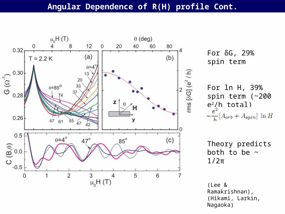
Angular Dependence of R(H) profile Cont.
For δG, 29% spin term
For ln H, 39% spin term (~200 e2/h total)
Theory predicts both to be ~ 1/2π
(Lee & Ramakrishnan), (Hikami, Larkin, Nagaoka)

Conductance -- sum over Feynman paths
ji
i
jii
iji
jijieAAAAAG
,
)(
,
* ||||2
Universal conductance fluctuations (UCF)
G = e2/h
Universal Conductance Fluctuations
in a coherent volume defined by thermal length LT = hD/kT
At 1 K, LT ~ 1 m
For large samples size L, 212 /
L
L
h
eG T
H
LT
Stone, Lee, Fukuyama (PRB 1987)
LT
L = 2 mm“Central-limit theorem”
UCF should be unobservable in a 2-mm crystal!
Quantum diffusion
our xtal

Taking typical 2D LT = 1 µm at 1 K,
For systems size L > LT, consider (L/LT)d systems of size LT, UCF suppressed as
For AB oscillation, assuming 60 nm rings, N-1/2
~ 10-8
Size Scales
2/2)/( dT LL
TkDL
DL
BT
in
/
heGmeasured /~ 2
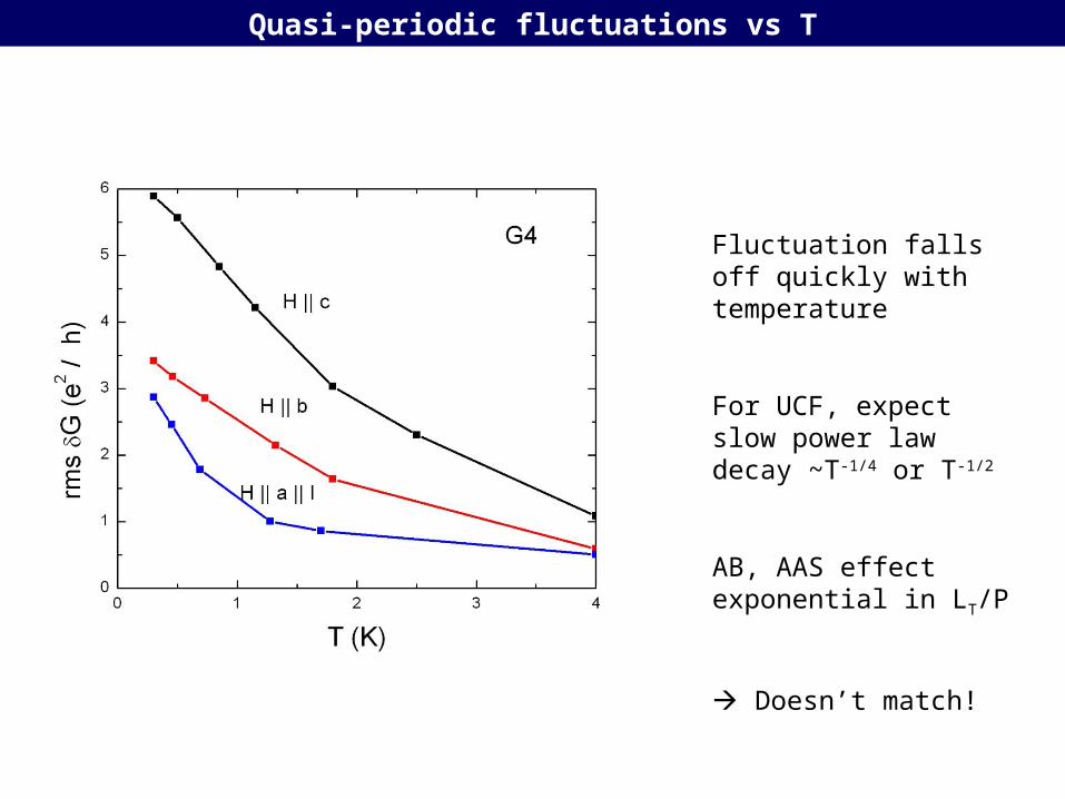
Quasi-periodic fluctuations vs T
Fluctuation falls off quickly with temperature
For UCF, expect slow power law decay ~T-1/4 or T-1/2
AB, AAS effect exponential in LT/P
Doesn’t match!

Non-Metallic Samples in High Field
Fluctuation does not change character significantly in enhanced field

Next Approach: Micro Samples

Micro Samples Cont.
Sample is gate-able
SdH signal not seen in 10 nm thick metallic sample
Exploring Callan-Harvey effect in a cleaved crystal
x

(b)
(c)
(a)

Desperately seeking Majorana bound state
SC1 SC2
(x)Majorana bound state
= 0 =
Open at byProximity effect
Surface topological states Fu and Kane, PRL 08
bound state wfelectron creation oper.
Neutral fermion that is its own anti-particle
Majorana oper.
Gap “twist” trapsMajorana)]()()()([ 2,1
2/*2,1
2/2,1 xcxexcxedx ii

Cu Doping: Intercalation between Layers
Hor et al., arXiv 0909.2890
Intercalation of Cu between layers
Confirmed by c-axis lattice parameter increase and STM data
Crystal quality checked by X-ray diffraction and electron diffraction
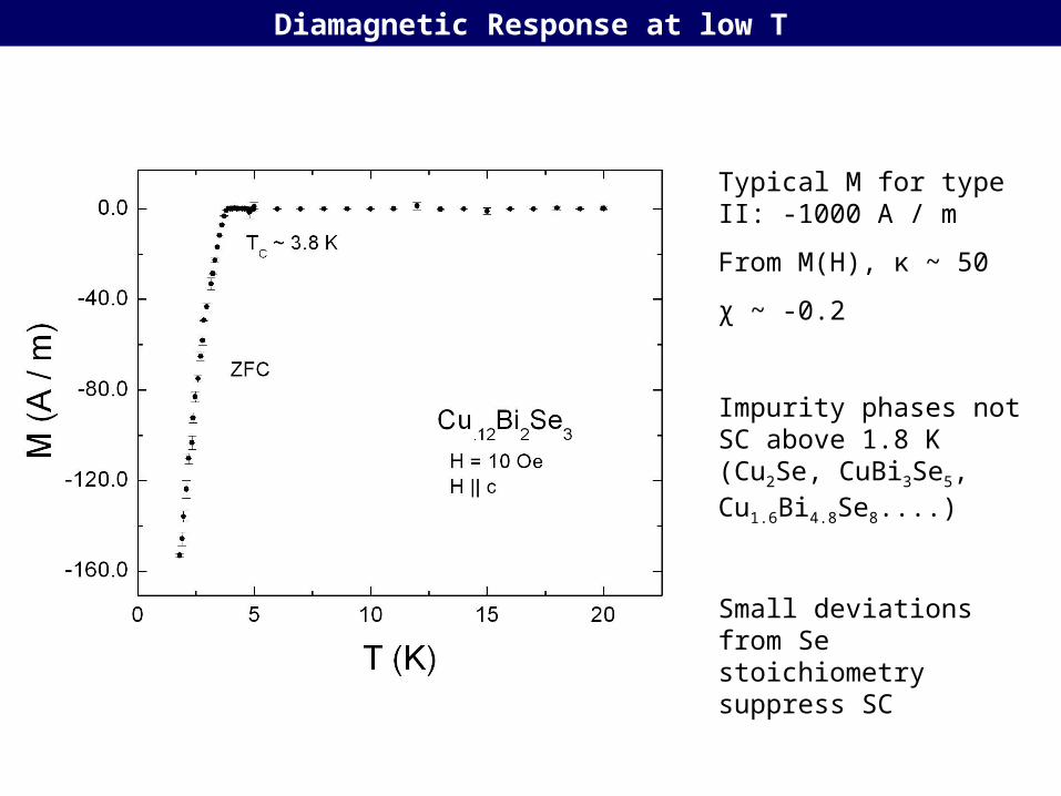
Diamagnetic Response at low T
Typical M for type II: -1000 A / m
From M(H), κ ~ 50
χ ~ -0.2
Impurity phases not SC above 1.8 K (Cu2Se, CuBi3Se5, Cu1.6Bi4.8Se8....)
Small deviations from Se stoichiometry suppress SC

Cu Doping: Transport Properties
Not complete resistive transition
Up to 80% transition has been seen
Carrier density relatively high

Upper Critical Field HC2
HC2 anisotropy moderate
ξc = 52 Å , ξab = 140 Å
HC2 estimate by extrapolation
Similar shape for H||ab

Ca Doping: Conclusions
Ca doping can bring samples from n-type to p-type
Non-metallic samples at threshold between the two reveal new transport properties
G ~ ln(H) at low H
δG ~ e2/h, quasiperiodic
Hard to fit with mesoscopic interpretation
No LL quantization seen up to 32 T
Metallic nanoscale samples show no LL
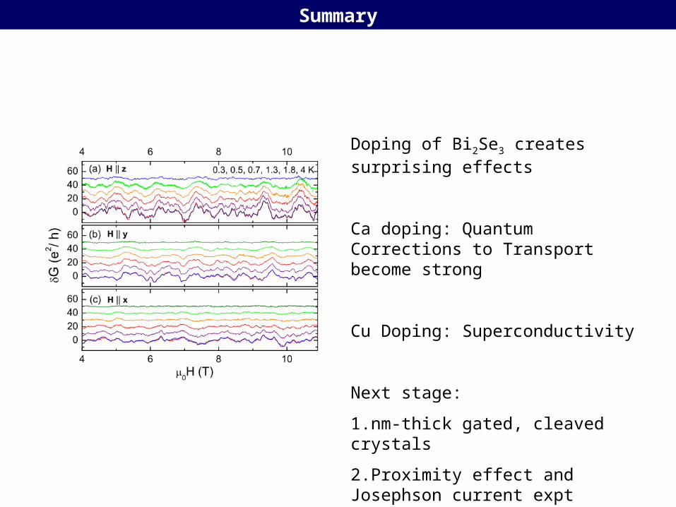
Summary
Doping of Bi2Se3 creates surprising effects
Ca doping: Quantum Corrections to Transport become strong
Cu Doping: Superconductivity
Next stage:
1.nm-thick gated, cleaved crystals
2.Proximity effect and Josephson current expt

END