Embed Size (px)
Citation preview

UNIT IV
MEMORY DEVICES
1

Integrated Circuits
• A collection of one or more gates fabricated on a single silicon chip is called an integrated circuit (IC).
• ICs were classified by size:– SSI - small scale integration - 1~20 gates– MSI - medium scale integration - 20~200 gates– LSI - large scale integration - 200~200,000 gates– VLSI - very large scale integration - over 1M
transistors
• Pentium-III - 40 million transistors2

UNIT V
MEMORY AND PROGRAMMABLE LOGIC
Integration level Number of transistors
Zero scale integration (ZSI) 1
Small scale integration (SSI) 2–30
Medium scale integration (MSI) 30 - 103
Large scale integration (LSI) 103 - 105
Very large scale integration (VLSI) 105 – 107
Ultra large scale integration (ULSI) 107 – 109
Giga-scale integration (GSI) 109 – 1011
Tera-scale integration (TSI) 1011 – 1013
3

• n data lines (input/output)• k address lines• 2k words (data unit)• Read/Write Control• Memory size = 2k X n
Memory
A Memory is a device in which binary information can be stored (write) and later retrieved (read)
4

Density - Amount of data that the memory can store
(Non-) Volatility - Data storage capability if power is disconnected
Read/write capability - Capability to update memory
Memory
Three Important Characteristics of Semiconductor Memory:
5

Memory
Memory is required to store:
1. data
2. application programs
3. operating system

Memory
Can be broadly classified as:
Random Access Memory (RAM)
or
Read Only Memory (ROM)

8
Random Access Memory (RAM) Can be written to or read from.
Read/Write memory Reading from RAM is non-destructive. Access time to read from any memory location
is the same. As compared to serial access memory.
Volatile Information is lost when power is removed.

9
Random Access Memory (RAM)
Random Access Memory (RAM) Static Random Access Memory (SRAM)
Based on the Flip-Flop Requires a large number of transistors Fast
Dynamic Random Access Memory (DRAM) Uses a single transistor to store charge Requires very few transistors Must be periodically refreshed Slow(er)

11
Read Only Memory (ROM) Can only be read from. Memory is written (or “programmed”) once Reading from ROM is non-destructive. Access time to read from any memory
location is the same. As compared to serial access memory.
Non-Volatile Information is retained even after power is
removed.

12
Read Only Memory (ROM) Programmable Read Only Memory (PROM)
Can be “programmed” Erasable PROM (EPROM)
Can be “programmed” and erased Electrically Erasable PROM (EEPROM)
Can be erased using an electrical signal UV Erasable PROM (UVEPROM)
Can be erased using Ultraviolet light

Mask ROM• The mask ROM is usually referred to simply as a ROM.
• A regular ROM is constructed from hard-wired logic, encoded in the silicon itself to perform a specific function that cannot be changed.
• They consume very little power and reliable but cannot reprogram or rewrite.
• Several types of user programmable ROMs have been developed to overcome this disadvantage.

Programmable ROM (PROM)
• A mask ROM chip is very expensive and time-consuming to create in small quantities from scratch.
• Mainly, developers created a type of ROM known as programmable read-only memory (PROM).
• This is basically a blank ROM chip that can be written only once using special equipment called a PROM programmer.
• PROM chips have a grid of columns and rows just as ordinary ROMs do.

• The difference is that every intersection of a column and row in a PROM chip has a fuse connecting them.
• Since all the cells have a fuse, the initial (blank) state of a PROM chip is all 1s.
• The user cans selectively burn/blow any of these fuse links to produce the desired stored memory data.
• A charge sent through a column will pass through the fuse in a cell to a grounded row indicating a value of 1.
Programmable ROM (PROM)

• To change the value of a cell to 0, you use a PROM programmer to send a specific amount of current to the cell to break the connection between the column and row by burning out the fuse.
• This process is known as burning the PROM.
• Very few bipolar PROMs are still available today.
• TMS27PC256 is a very popular CMOS PROM with a capacity of 32K 8.
Programmable ROM (PROM)

Erasable Programmable ROM (EPROM)
• An EPROM is a ROM that can be erased and reprogrammed as often as desired. Once programmed.
• The EPROM is a non-volatile memory that will hold its stored data indefinitely.
• A little glass window is provided in the top of the ROM package.
• Ultraviolet light of a specific frequency can be shined through this window for a specified period of time, which will erase all cells at the same time so that an erased EPROM stores all 1s and allow it to be reprogrammed again.

Erasable Programmable ROM (EPROM)
• EPROMs are configured using an EPROM programmer that provides voltage at specified levels depending on the type of EPROM used.
• Obviously this is much more useful than a regular PROM, but it does require the erasing light.
• EPROMs are available in a wide range of capacities and access times. The 27C64 is an example of 8K x 8 CMOS EPROM

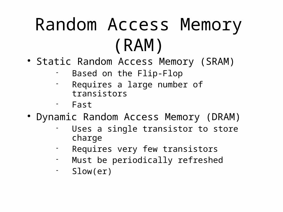
Electrically Erasable Programmable ROM (EEPROM)
• They require dedicated equipment and a labor-intensive process to remove and reinstall them each time a change is necessary.
• The next type of ROM is the EEPROM, which can be erased under software control.
• This is the most flexible type of ROM, and is now commonly used for holding BIOS programs
Electrically Erasable Programmable ROM (EEPROM)
• In EEPROMs the chip does not have to be removed to be rewritten, the entire chip need not be fully erased to change a specific portion of it, and changing the contents does not require additional dedicated equipment.
• Instead of using UV light, you can return the electrons in the cells of an EEPROM to normal with the localized application of an electric field to each cell.

Electrically Erasable Programmable ROM (EEPROM)
• This erases the targeted cells of the EEPROM, which can then be rewritten.
• EEPROMs are changed 1 byte at a time, which makes them versatile but slow.
• The Intel 2864 is an example of EEPROM with 8K 8 array with 13 address inputs and eight data I/O pins

Flash Memory
• Flash memories are so called because of their rapid erase and write times.
• EEPROM chips speed is too slow to use in many products that required quick changes to the data stored on the chip.
• So a new type of EEPROM called Flash memory that uses in-circuit wiring to erase by applying an electrical field to the entire chip or to predetermined sections of the chip called blocks.

Flash Memory
• Flash memory works much faster than traditional EEPROMs because it writes data in chunks, usually 512 bytes in size, instead of 1 byte at a time.
• The 28F256A CMOS IC is an example of flash memory chip, which has a capacity of 32K 8.

Types of RAM
RAM
SRAM DRAM
RAM is volatile. It will lose information when the power is turned off.
24

Memory (cont.)• Random Access Memory (RAM):
• Write/Read operations• Volatile: Data is lost when power is turned
off
• Read Only Memory (ROM): • Read operation (no write)• Non-Volatile: Data is permanent.• PROM is programmable (allow special
write)
25

Random Access Memory (RAM)
Can be written to or read from. Read/Write memory
Reading from RAM is non-destructive. Access time to read from any memory
location is the same. As compared to serial access memory.
Volatile Information is lost when power is removed.
26

27
Random Access Memory
27

28
Random Access Memory Rather than use the Read and Write
signals, most commercially available RAM chips use Enable and Read/Write'
Enable Used to enable the selected RAM chip “chip select”
Read/Write' RAM is read when Read/Write' = 1 RAM is written when Read/Write' = 0
28

29
Random Access Memory
29

30
Random Access Memory
Write Cycle
30
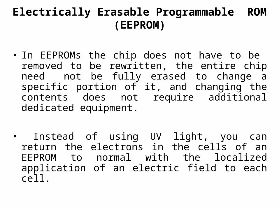
31
Random Access Memory
Read Cycle
31

32
Random Access Memory
32

33
Random Access Memory (RAM)
Static Random Access Memory (SRAM) Based on the Flip-Flop Requires a large number of transistors Fast
Dynamic Random Access Memory (DRAM) Uses a single transistor to store charge Requires very few transistors Must be periodically refreshed Slow(er)
33

34
RAM: Address Decoding k-bit address
Decoder requires 2k AND gates Each AND gate has k inputs
For large k this becomes prohibitive. Use 2-dimensional decoding
Two decoders Each decoder requires 2(k/2) AND
gates Each AND gate has k/2 inputs
Far less combinational logic
34

3535
RAM: Address Decoding

3636
RAM: Address Decoding The size of a chip package is often dictated
by the number of input and output signals. For large memories, the number of address
lines often becomes prohibitive. Use address multiplexing
The same address lines are used both for the row address and the column address
Use time multiplexing to first latch the row address and then latch the column address

3737
Exercise: 32K x 32 RAM
Addr Addr Addr Addr15
A14
- A0
D31
- D24
8 8 8 8
D23
- D16
D15
- D8
D7 - D
0
Data Data Data Data

3838
RAM Systems
Exercise:
Design a 128K x 8 memory using
RAM chips that are 32K x 8.
How many address bits are required?How many address bits are connected to the RAM chips?
What are the remaining address bits connected to?

3939
Example: 128K x 8 RAM

4040
RAM Systems
Exercise:
Design a 32K x 32 memory using
RAM chips that are 32K x 8.
How many address bits are required?How many data bits are required?

SRAM

SRAM operation• Individual bits are D latches, not
edge-triggered D flip-flops.– Fewer transistors per cell.
• Implications for write operations:– Address must be stable before writing cell.– Data must be stable before ending a write.

SRAM array

SRAM control lines
• Chip select• Output enable• Write enable

SRAM read timing
• Similar to ROM read timing

SRAM write timing
• Address must be stable before and after write-enable is asserted.
• Data is latched on trailing edge of (WE & CS).

DRAM (Dynamic RAMs)• SRAMs typically use six transistors per
bit of storage.
• DRAMs use only onetransistor per bit:
• 1/0 = capacitorcharged/discharged

DRAM read operations
– Precharge bit line to VDD/2.
– Take the word line HIGH.– Detect whether current flows into or out of the cell.– Note: cell contents are destroyed by the read!– Must write the bit value back after reading.

DRAM write operations
– Take the word line HIGH.– Set the bit line LOW or HIGH to store 0 or 1.– Take the word line LOW.
– Note: The stored charge for a 1 will eventually leak off.

DRAM charge leakage
• Typical devices require each cell to be refreshed once every 4 to 64 mS.
• During “suspended” operation, notebook computers use power mainly for DRAM refresh.

DRAM-chip internal organization
64K x 1DRAM

RAS/CAS operation
• Row Address Strobe, Column Address Strobe– n address bits are provided in two steps using n/2
pins, referenced to the falling edges of RAS_L and CAS_L
– Traditional method of DRAM operation for 20 years.
– Now being supplanted by synchronous, clocked interfaces in SDRAM (synchronous DRAM).

DRAM read timing

DRAM refresh timing
DRAM refresh timing
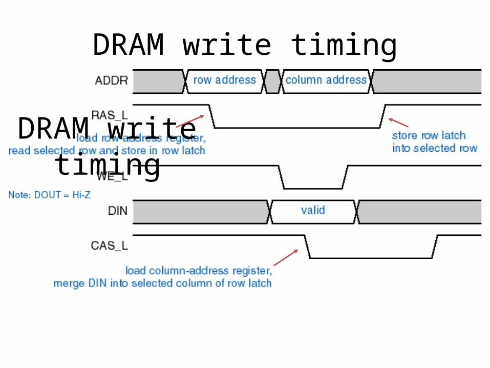
DRAM write timing
DRAM write timing

• PLDs
– Programmable Logic Devices (PLD)• General purpose chip for implementing circuits• Can be customized using programmable switches
– Main types of PLDs• PLA• PAL• ROM• CPLD• FPGA
– Custom chips: standard cells, sea of gates

• Programmable Logic Array (PLA)
– Use to implement circuits in SOP form
– The connections inthe AND plane areprogrammable
– The connections inthe OR plane areprogrammable
f 1
AND plane OR plane
Input buffers
inverters and
P 1
P k
f m
x 1 x 2 x n
x 1 x 1 x n x n

• Gate Level Version of PLA
f1
P1
P2
f2
x1 x2 x3
OR plane
Programmable
AND plane
connections
P3
P4
f1 = x1x2+x1x3'+x1'x2'x3
f2 = x1x2+x1'x2'x3+x1x3

• Customary Schematic of a PLA
f1 = x1x2+x1x3'+x1'x2'x3
f2 = x1x2+x1'x2'x3+x1x3
f 1
P 1
P 2
f 2
x 1 x 2 x 3
OR plane
AND plane
P 3
P 4
x marks the connections left in place after programming

• Limitations of PLAs
– PLAs come in various sizes• Typical size is 16 inputs, 32 product terms, 8 outputs
– Each AND gate has large fan-in this limits the number of inputs that can be provided in a PLA
– 16 inputs 316 = possible input combinations; only 32 permitted (since 32 AND gates) in a typical PLA
– 32 AND terms permitted large fan-in for OR gates as well
» This makes PLAs slower and slightly more expensive than some alternatives to be discussed shortly
– 8 outputs could have shared minterms, but not required

• Programmable Array Logic (PAL)
– Also used to implement circuits in SOP form
– The connections inthe AND plane areprogrammable
– The connections inthe OR plane areNOT programmable
f 1
AND plane OR plane
Input buffers
inverters and
P 1
P k
f m
x 1 x 2 x n
x 1 x 1 x n x n
fixed connections

• Example Schematic of a PAL
f 1
P 1
P 2
f 2
x 1 x 2 x 3
AND plane
P 3
P 4
f1 = x1x2x3'+x1'x2x3
f2 = x1'x2'+x1x2x3

• Comparing PALs and PLAs
– PALs have the same limitations as PLAs (small number of allowed AND terms) plus they have a fixed OR plane less flexibility than PLAs
– PALs are simpler to manufacture, cheaper, and faster (better performance)
– PALs also often have extra circuitry connected to the output of each OR gate
• The OR gate plus this circuitry is called a macrocell

• Multi-Level Design with PALs
– f = A'BC + A'B'C' + ABC' + AB'C = A'g + Ag'• where g = BC + B'C' and C = h below
D Q
Clock
Sel = 0En = 0
0
1
D Q
Clock
Select
0
1
D Q
Clock
Sel = 0En = 1
0
1
A B
h
g
f

• FPGA
– SPLDs and CPLDs are relatively small and useful for simple logic devices
• Up to about 20000 gates
– Field Programmable Gate Arrays (FPGA) can handle larger circuits
• No AND/OR planes• Provide logic blocks, I/O blocks, and interconnection wires
and switches
• Logic blocks provide functionality• Interconnection switches allow logic blocks to be connected
to each other and to the I/O pins

• Structure of an FPGA
I/O block
I/O block I/O
blo
ck I/O
blo
ck
logic block
interconnectionswitch

• Programming an FPGA
– ISP method is used
– LUTs contain volatile storage cells• None of the other PLD technologies are volatile• FPGA storage cells are loaded via a PROM when power is
first applied
– The UP2 Education Board by Altera contains a JTAG port, a MAX 7000 CPLD, and a FLEX 10K FPGA
• The MAX 7000 CPLD chip is EPM7128SLC84-7• EPM7 MAX 7000 family; 128 macrocells; LC84 84 pin
PLCC package; 7 speed grade

• Example FPGA
– Use an FPGA with 2 input LUTS to implement the function f = x1x2 + x2'x3
• f1 = x1x2
• f2 = x2'x3
• f = f1 + f20 1 0 0
0 1 1 1
0 0 0 1
x 1
x 2
x 2
x 3
f 1
f 2
f 1 f 2
f
x 1
x 2
x 3 f

• Another Example FPGA
– Use an FPGA with 2 input LUTS to implement the function f = x1x3x6' + x1x4x5x6' + x2x3x7 + x2x4x5x7
• Fan-in of expression is too large for FPGA (this was simple to do in a CPLD)
• Factor f to get sub-expressions with max fan-in = 2– f = x1x6'(x3 + x4x5) + x2x7(x3 + x4x5)
= (x1x6' + x2x7)(x3 + x4x5)
• Could use Shannon's expansion instead– Goal is to build expressions out of 2-input LUTs

0 0 0 1
0 1 1 1
x 4
x 5
A
B
C
D
x 1
x 6
x 4 f
0 1 1 1
0 0 0 1
x 3
C
D
E
E
f
x 2
x 7
x 5 x 3
0 0 0 1
x 2
x 7
B
0 0 1 0
x 1
x 6
A
• FPGA Implementation
– f = (x1x6' + x2x7)(x3 + x4x5)

• Digital Logic Technology Tradeoffs
Engineering cost / Time to develop
Speed / Density / Complexity / LikelyMarket Volume
PLDs
CPLDsFPGAs
ASICs
Full customVLSI design