Embed Size (px)
Citation preview

UNIT III
DATA-LEVEL PARALLELISM IN VECTOR, SIMD, AND GPU
ARCHITECTURES
Flynn’s Taxonomy
Single instruction stream, single data stream (SISD)
Single instruction stream, multiple data streams (SIMD)
o Vector architectures
o Multimedia extensions
o Graphics processor units
Multiple instruction streams, single data stream (MISD)
o No commercial implementation
Multiple instruction streams, multiple data streams (MIMD)
o Tightly-coupled MIMD
Loosely-coupled MIMD
Introduction
SIMD architectures can exploit significant data-level parallelism for:
matrix-oriented scientific computing
media-oriented image and sound processors
SIMD is more energy efficient than MIMD
Only needs to fetch one instruction per data operation
Makes SIMD attractive for personal mobile devices
SIMD allows programmer to continue to think sequentially
SIMD Parallelism
Vector architectures
SIMD extensions
Graphics Processor Units (GPUs)
For x86 processors:
Expect two additional cores per chip per year
SIMD width to double every four years
Potential speedup from SIMD to be twice that from MIMD!
Figure 3.1 Potential speedup via parallelism from MIMD, SIMD, and both MIMD and
SIMD over time for x86 computers.
This figure assumes that two cores per chip for MIMD will be added every two years and the
number of operations for SIMD wills double every four years.
Vector Architectures
Basic idea:
Read sets of data elements into “vector registers”
Operate on those registers
Disperse the results back into memory

Registers are controlled by compiler
Used to hide memory latency
Leverage memory bandwidth
VMIPS
Example architecture: VMIPS
Loosely based on Cray-1
Vector registers
Each register holds a 64-element, 64 bits/element vector
Register file has 16 read ports and 8 write ports
Vector functional units
Fully pipelined
Data and control hazards are detected
Vector load-store unit
Fully pipelined
One word per clock cycle after initial latency
Scalar registers
32 general-purpose registers
32 floating-point registers
Figure 3.2 the basic structure of vector architecture, VMIPS.
This processor has a scalar architecture just like MIPS. There are also eight 64-element vector
registers, and all the functional units are vector functional units. This chapter defines special
vector instructions for both arithmetic and memory accesses. The figure shows vector units for
logical and integer operations so that VMIPS looks like a standard vector processor that usually
include these units; however, we will not be discussing these units. The vector and scalar
registers have a significant number of read and write ports to allow multiple simultaneous vector
operations. A set of crossbar switches (thick gray lines) connects these ports to the inputs and
outputs of the vector functional units.
VMIPS Instructions
ADDVV.D: add two vectors
ADDVS.D: add vector to a scalar
LV/SV: vector load and vector store from address
Example: DAXPY (double precision a*X+Y)
L.D F0,a ; load scalar a
LV V1,Rx ; load vector X
MULVS.D V2,V1,F0 ; vector-scalar multiply
LV V3,Ry ; load vector Y
ADDVV V4,V2,V3 ; add
SV Ry,V4 ; store the result
Requires 6 instructions
DAXPY in MIPS Instructions
Example: DAXPY (double precision a*X+Y)
L.D F0,a ; load scalar a
DADDIU R4,Rx,#512 ; last address to load
Loop: L.D F2,0(Rx) ; load X[i]
MUL.D F2,F2,F0 ; a x X[i]
L.D F4,0(Ry) ; load Y[i]
ADD.D F4,F2,F2 ; a x X[i] + Y[i]
S.D F4,9(Ry) ; store into Y[i]
DADDIU Rx,Rx,#8 ; increment index to X
DADDIU Ry,Ry,#8 ; increment index to Y
SUBBU R20,R4,Rx ; compute bound
BNEZ R20,Loop ; check if done
Requires almost 600 MIPS ops
Vector Execution Time
Execution time depends on three factors:
Length of operand vectors
Structural hazards

Data dependencies
VMIPS functional units consume one element per clock cycle
Execution time is approximately the vector length
Convoy
Set of vector instructions that could potentially execute together
Sequences with read-after-write dependency hazards can be in the same convey via
chaining
Chaining
Allows a vector operation to start as soon as the individual elements of its vector
source operand become available
Chime
Unit of time to execute one convey
m conveys executes in m chimes
For vector length of n, requires m x n clock cycles
Example
LV V1, Rx ; load vector X
MULVS.D V2, V1, F0 ; vector-scalar multiply
LV V3, Ry ; load vector Y
ADDVV.D V4, V2, V3 ; add two vectors
SV Ry, V4 ; store the sum
Convoys:
1 LV MULVS.D
2 LV ADDVV.D
3 SV
3 chimes, 2 FP ops per result, cycles per FLOP = 1.5
For 64 element vectors, requires 64 x 3 = 192 clock cycles
Challenges
Start up time
Latency of vector functional unit
Assume the same as Cray-1
Floating-point add => 6 clock cycles
Floating-point multiply => 7 clock cycles
Floating-point divide => 20 clock cycles
Vector load => 12 clock cycles
Optimizations:
Multiple Lanes: > 1 element per clock cycle
Vector Length Registers: Non-64 wide vectors
Vector Mask Registers: IF statements in vector code
Memory Banks: Memory system optimizations to support vector processors
Stride: Multiple dimensional matrices
Scatter-Gather: Sparse matrices
Programming Vector Architectures: Program structures affecting performance
Multiple Lanes
Element n of vector register A is “hardwired” to element n of vector register B
Allows for multiple hardware lanes

Figure 3.3 Diagrams of Multiple Lanes

Vector Length Registers
Vector length not known at compile time?
Use Vector Length Register (VLR)
Use strip mining for vectors over the maximum length:
low = 0;
VL = (n % MVL); /*find odd-size piece using modulo op % */
for (j = 0; j <= (n/MVL); j=j+1) { /*outer loop*/
for (i = low; i < (low+VL); i=i+1) /*runs for length VL*/
Y[i] = a * X[i] + Y[i] ; /*main operation*/
low = low + VL; /*start of next vector*/
VL = MVL; /*reset the length to maximum vector length*/
}
Vector Mask Registers
Consider:
for (i = 0; i < 64; i=i+1)
if (X[i] != 0)
X[i] = X[i] – Y[i];
Use vector mask register to “disable” elements (if conversion):
LV V1,Rx ;load vector X into V1
LV V2,Ry ;load vector Y
L.D F0,#0 ;load FP zero into F0

SNEVS.D V1,F0 ;sets VM(i) to 1 if V1(i)!=F0
SUBVV.D V1,V1,V2 ;subtract under vector mask
SV Rx,V1 ;store the result in X
GFLOPS rate decreases!
Memory Banks
Memory system must be designed to support high bandwidth for vector loads and stores
Spread accesses across multiple banks
Control bank addresses independently
Load or store non sequential words
Support multiple vector processors sharing the same memory
Example:
32 processors, each generating 4 loads and 2 stores/cycle
Processor cycle time is 2.167 ns, SRAM cycle time is 15 ns
How many memory banks needed?
32x6=192 accesses,
15/2.167≈7 processor cycles
1344!
Stride
Consider:
for (i = 0; i < 100; i=i+1)
for (j = 0; j < 100; j=j+1) {
A[i][j] = 0.0;
for (k = 0; k < 100; k=k+1)
A[i][j] = A[i][j] + B[i][k] * D[k][j];
}
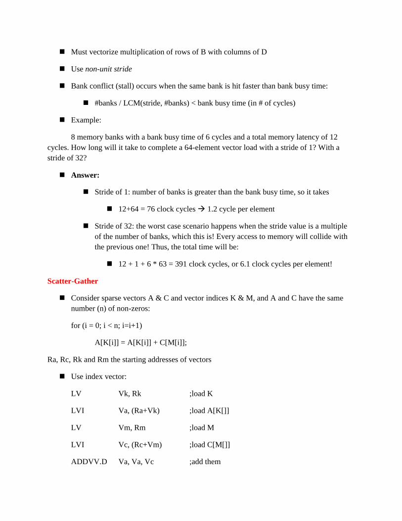
Must vectorize multiplication of rows of B with columns of D
Use non-unit stride
Bank conflict (stall) occurs when the same bank is hit faster than bank busy time:
#banks / LCM(stride, #banks) < bank busy time (in # of cycles)
Example:
8 memory banks with a bank busy time of 6 cycles and a total memory latency of 12
cycles. How long will it take to complete a 64-element vector load with a stride of 1? With a
stride of 32?
Answer:
Stride of 1: number of banks is greater than the bank busy time, so it takes
12+64 = 76 clock cycles 1.2 cycle per element
Stride of 32: the worst case scenario happens when the stride value is a multiple
of the number of banks, which this is! Every access to memory will collide with
the previous one! Thus, the total time will be:
12 + 1 + 6 * 63 = 391 clock cycles, or 6.1 clock cycles per element!
Scatter-Gather
Consider sparse vectors A & C and vector indices K & M, and A and C have the same
number (n) of non-zeros:
for (i = 0; i < n; i=i+1)
A[K[i]] = A[K[i]] + C[M[i]];
Ra, Rc, Rk and Rm the starting addresses of vectors
Use index vector:
LV Vk, Rk ;load K
LVI Va, (Ra+Vk) ;load A[K[]]
LV Vm, Rm ;load M
LVI Vc, (Rc+Vm) ;load C[M[]]
ADDVV.D Va, Va, Vc ;add them

SVI (Ra+Vk), Va ;store A[K[]]
SIMD Extensions
Media applications operate on data types narrower than the native word size
Example: disconnect carry chains to “partition” adder
Limitations, compared to vector instructions:
Number of data operands encoded into op code
No sophisticated addressing modes (strided, scatter-gather)
No mask registers
SIMD Implementations
Implementations:
Intel MMX (1996)
Eight 8-bit integer ops or four 16-bit integer ops
Streaming SIMD Extensions (SSE) (1999)
Eight 16-bit integer ops
Four 32-bit integer/fp ops or two 64-bit integer/fp ops
Advanced Vector Extensions (2010)
Four 64-bit integer/fp ops
Operands must be consecutive and aligned memory locations
Generally designed to accelerate carefully written libraries rather than for
compilers
Advantages over vector architecture:
Cost little to add to the standard ALU and easy to implement
Require little extra state easy for context-switch
Require little extra memory bandwidth
No virtual memory problem of cross-page access and page-fault

Example SIMD Code
Example DXPY:
L.D F0,a ;load scalar a
MOV F1, F0 ;copy a into F1 for SIMD MUL
MOV F2, F0 ;copy a into F2 for SIMD MUL
MOV F3, F0 ;copy a into F3 for SIMD MUL
DADDIU R4,Rx,#512 ;last address to load
Loop: L.4D F4,0[Rx] ;load X[i], X[i+1], X[i+2], X[i+3]
MUL.4D F4,F4,F0 ;a×X[i],a×X[i+1],a×X[i+2],a×X[i+3]
L.4D F8,0[Ry] ;load Y[i], Y[i+1], Y[i+2], Y[i+3]
ADD.4D F8,F8,F4 ;a×X[i]+Y[i], ..., a×X[i+3]+Y[i+3]
S.4D F8,0[Ry] ;store into Y[i], Y[i+1], Y[i+2], Y[i+3]
DADDIU Rx,Rx,#32 ;increment index to X
DADDIU Ry,Ry,#32 ;increment index to Y
DSUBU R20,R4,Rx ;compute bound
BNEZ R20,Loop ;check if done
Roofline Performance Model
Basic idea:
Plot peak floating-point throughput as a function of arithmetic intensity
Ties together floating-point performance and memory performance for a target
machine
Arithmetic intensity
Floating-point operations per byte read
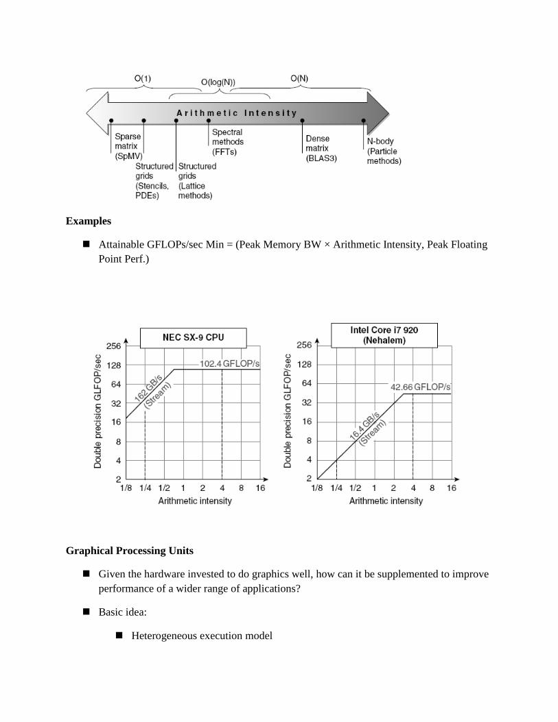
Examples
Attainable GFLOPs/sec Min = (Peak Memory BW × Arithmetic Intensity, Peak Floating
Point Perf.)
Graphical Processing Units
Given the hardware invested to do graphics well, how can it be supplemented to improve
performance of a wider range of applications?
Basic idea:
Heterogeneous execution model

CPU is the host, GPU is the device
Develop a C-like programming language for GPU
Compute Unified Device Architecture (CUDA)
OpenCL for vendor-independent language
Unify all forms of GPU parallelism as CUDA thread
Programming model is “Single Instruction Multiple Thread” (SIMT)
Threads and Blocks
A thread is associated with each data element
CUDA threads, with thousands of which being utilized to various styles of
parallelism: multithreading, SIMD, MIMD, ILP
Threads are organized into blocks
Thread Blocks: groups of up to 512 elements
Multithreaded SIMD Processor: hardware that executes a whole thread block (32
elements executed per thread at a time)
Blocks are organized into a grid
Blocks are executed independently and in any order
Different blocks cannot communicate directly but can coordinate using atomic
memory operations in Global Memory
GPU hardware handles thread management, not applications or OS
A multiprocessor composed of multithreaded SIMD processors

Figure 3.4 A Thread Block Scheduler consist of Grid, Threads, and Blocks
NVIDIA GPU Architecture
Similarities to vector machines:
Works well with data-level parallel problems
Scatter-gather transfers
Mask registers
Large register files
Differences:
No scalar processor
Uses multithreading to hide memory latency
Has many functional units, as opposed to a few deeply pipelined units like a vector processor
Example
Multiply two vectors of length 8192
Code that works over all elements is the grid
Thread blocks break this down into manageable sizes
512 elements/block, 16 SIMD threads/block 32 ele/thread
SIMD instruction executes 32 elements at a time
Thus grid size = 16 blocks
Block is analogous to a strip-mined vector loop with vector length of 32
Block is assigned to a multithreaded SIMD processor by the thread block
scheduler
Current-generation GPUs (Fermi) have 7-15 multithreaded SIMD processors

Figure 3.5 .Floor plan of the Fermi GTX 480 GPU.
This diagram shows 16 multithreaded SIMD Processors. The Thread Block Scheduler is
highlighted on the left. The GTX 480 has 6 GDDR5 ports, each 64 bits wide, supporting up to 6
GB of capacity. The Host Interface is PCI Express 2.0 x 16. Giga Thread is the name of the
scheduler that distributes thread blocks to Multiprocessors, each of which has its own SIMD
Thread Scheduler.
Terminology
Threads of SIMD instructions
Each has its own PC
Thread scheduler uses scoreboard to dispatch
No data dependencies between threads!
Keeps track of up to 48 threads of SIMD instructions
Hides memory latency
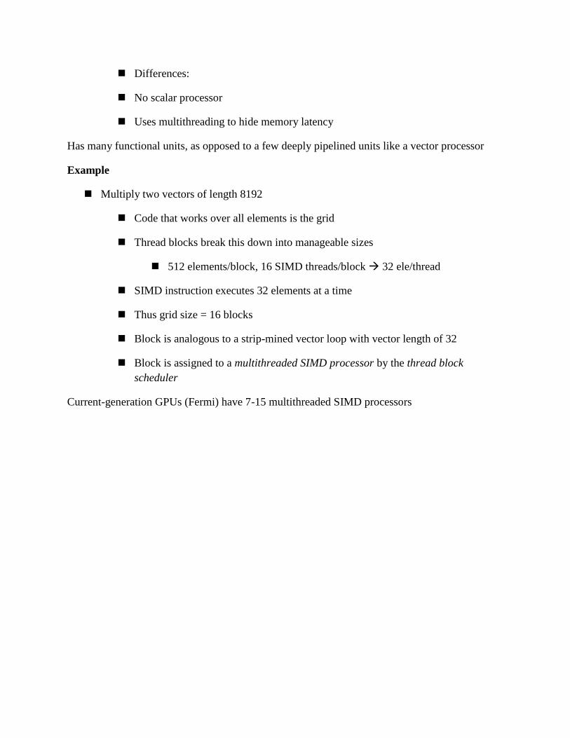
Thread block scheduler schedules blocks to SIMD processors
Within each SIMD processor:
32 SIMD lanes
Wide and shallow compared to vector processors
Figure 3.6 Scheduling of threads of SIMD instructions.
The scheduler selects a ready thread of SIMD instructions and issues an instruction
synchronously to all the SIMD Lanes executing the SIMD thread. Because threads of SIMD
instructions are independent, the scheduler may select a different SIMD thread each time.
Example
NVIDIA GPU has 32,768 registers
Divided into lanes
Each SIMD thread is limited to 64 registers
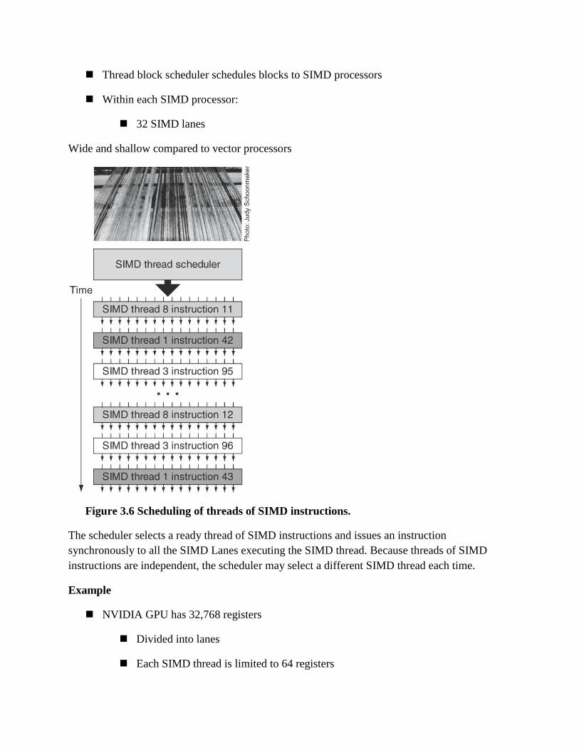
SIMD thread has up to:
64 vector registers of 32 32-bit elements
32 vector registers of 32 64-bit elements
Fermi has 16 physical SIMD lanes, each containing 2048 registers
Figure 3.7 Simplified block diagram of a Multithreaded SIMD Processor.
It has 16 SIMD lanes. The SIMD Thread Scheduler has, say, 48 independentthreads of SIMD
instructions that it schedules with a table of 48 PCs.
NVIDIA Instruction Set Arch.
ISA is an abstraction of the hardware instruction set
“Parallel Thread Execution (PTX)”
Uses virtual registers

Translation to machine code is performed in software
Example: one CUDA thread, 8192 of these created!
shl.s32 R8, blockIdx, 9 ; Thread Block ID * Block size (512 or 29)
add.s32 R8, R8, threadIdx ; R8 = i = my CUDA thread ID
ld.global.f64 RD0, [X+R8] ; RD0 = X[i]
ld.global.f64 RD2, [Y+R8] ; RD2 = Y[i]
mul.f64 R0D, RD0, RD4 ; Product in RD0 = RD0 * RD4 (scalar a)
add.f64 R0D, RD0, RD2 ; Sum in RD0 = RD0 + RD2 (Y[i])
st.global.f64 [Y+R8], RD0 ; Y[i] = sum (X[i]*a + Y[i])
Conditional Branching
Like vector architectures, GPU branch hardware uses internal masks
Also uses
Branch synchronization stack
Entries consist of masks for each SIMD lane
I.e. which threads commit their results (all threads execute)
Instruction markers to manage when a branch diverges into multiple execution
paths
Push on divergent branch
…and when paths converge
Act as barriers
Pops stack
Per-thread-lane 1-bit predicate register, specified by programmer
Example
if (X[i] != 0)
X[i] = X[i] – Y[i];

else X[i] = Z[i];
ld.global.f64 RD0, [X+R8] ; RD0 = X[i]
setp.neq.s32 P1, RD0, #0 ; P1 is predicate register 1
@!P1, bra ELSE1, *Push ; Push old mask, set new mask bits
; if P1 false, go to ELSE1
ld.global.f64 RD2, [Y+R8] ; RD2 = Y[i]
sub.f64 RD0, RD0, RD2 ; Difference in RD0
st.global.f64 [X+R8], RD0 ; X[i] = RD0
@P1, bra ENDIF1, *Comp ; complement mask bits
; if P1 true, go to ENDIF1
ELSE1: ld.global.f64 RD0, [Z+R8] ; RD0 = Z[i]
st.global.f64 [X+R8], RD0 ; X[i] = RD0
ENDIF1: <next instruction>, *Pop ; pop to restore old mask
NVIDIA GPU Memory Structures
Each SIMD Lane has private section of off-chip DRAM
“Private memory”, not shared by any other lanes
Contains stack frame, spilling registers, and private variables
Recent GPUs cache this in L1 and L2 caches
Each multithreaded SIMD processor also has local memory that is on-chip
Shared by SIMD lanes / threads within a block only
The off-chip memory shared by SIMD processors is GPU Memory
Host can read and write GPU memory

Figure 3.8 GPU Memory structures.
GPU Memory is shared by all Grids (vectorized loops), Local Memory is shared by all threads
of SIMD instructions within a thread block (body of a vectorized loop), and Private Memory is
private to a single CUDA Thread.
Fermi Architecture Innovations
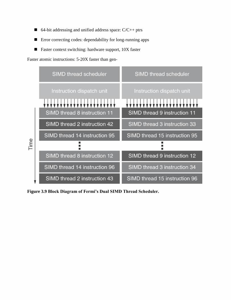
Each SIMD processor has
Two SIMD thread schedulers, two instruction dispatch units
16 SIMD lanes (SIMD width=32, chime=2 cycles), 16 load-store units, 4 special
function units
Thus, two threads of SIMD instructions are scheduled every two clock cycles
Fast double precision: gen- 78 515 GFLOPs for DAXPY
Caches for GPU memory: I/D L1/SIMD proc and shared L2
64-bit addressing and unified address space: C/C++ ptrs
Error correcting codes: dependability for long-running apps
Faster context switching: hardware support, 10X faster
Faster atomic instructions: 5-20X faster than gen-
Figure 3.9 Block Diagram of Fermi’s Dual SIMD Thread Scheduler.

Fermi Multithreaded SIMD Processor
Figure 3.10 Fermi Multithreaded SIMD Proc
Loop-Level Parallelism
Focuses on determining whether data accesses in later iterations are dependent on data
values produced in earlier iterations
Loop-carried dependence
Example 1:
for (i=999; i>=0; i=i-1)

x[i] = x[i] + s;
No loop-carried dependence
Example 2:
for (i=0; i<100; i=i+1) {
A[i+1] = A[i] + C[i]; /* S1 */
B[i+1] = B[i] + A[i+1]; /* S2 */
}
S1 and S2 use values computed by S1 in previous iteration
S2 uses value computed by S1 in same iteration
Example 3:
for (i=0; i<100; i=i+1) {
A[i] = A[i] + B[i]; /* S1 */
B[i+1] = C[i] + D[i]; /* S2 */
}
S1 uses value computed by S2 in previous iteration but dependence is not circular so loop
is parallel
Transform to:
A[0] = A[0] + B[0];
for (i=0; i<99; i=i+1) {
B[i+1] = C[i] + D[i];
A[i+1] = A[i+1] + B[i+1];
}
B[100] = C[99] + D[99];