Embed Size (px)
Citation preview

UNIT - I
Difference between Microprocessor and microcontroller
Microprocessor Micro Controller
Microprocessor is heart of Computer system. Micro Controller is a heart of embedded system.
It is just a processor. Memory and I/O components have to be connected externally
Micro controller has processor along with internal memory and i/O components
Since memory and I/O has to be connected externally, the circuit becomes large.
Since memory and I/O are present internally, the circuit is small.
Cannot be used in compact systems and hence inefficient
Can be used in compact systems and hence it is an efficient technique
Cost of the entire system increases Cost of the entire system is low
Due to external components, the entire power consumption is high. Hence it is not suitable to used with devices running on stored power like batteries.
Since external components are low, total power consumption is less and can be used with devices running on stored power like batteries.
Most of the microprocessors do not have power saving features.
Most of the micro controllers have power saving modes like idle mode and power saving mode. This helps to reduce power consumption even further.
Since memory and I/O components are all external, each instruction will need external operation, hence it is relatively slower.
Since components are internal, most of the operations are internal instruction, hence speed is fast.
Microprocessor have less number of registers, hence more operations are memory based.
Micro controller have more number of registers, hence the programs are easier to write.
Microprocessors are based on von Neumann model/architecture where program and data are stored in same memory module
Micro controllers are based on Harvard architecture where program memory and Data memory are separate
Mainly used in personal computers Used mainly in washing machine, MP3 players

8051 Microcontroller
The INTEL 8051 is an 8 bit microcontroller with 128 byte internal RAM and 4K bytes internal ROM. The 8051 is a 40 pin IC available in Dual in line package (DIP) and it requires a single power supply of +5V.
Pin Diagram

Pin-40 : Named as Vcc is the main power source. Usually its +5V DC.Pins 32-39: Known as Port 0 (P0.0 to P0.7) – In addition to serving as I/O port, lower order address and data bus signals are multiplexed with this port (to serve the purpose of external memory interfacing). This is a bi directional I/O port (the only one in 8051) and external pull up resistors are required to function this port as I/O.
Pin-31:- ALE aka Address Latch Enable is used to demultiplex the address-data signal of port 0 (for external memory interfacing.) 2 ALE pulses are available for each machine cycle.
Pin-30:- EA/ External Access input is used to enable or disallow external memory interfacing. If there is no external memory requirement, this pin is pulled high by connecting it to Vcc.
Pin- 29:- PSEN or Program Store Enable is used to read signal from external program memory.
Pins- 21-28:- Known as Port 2 (P 2.0 to P 2.7) – in addition to serving as I/O port, higher order address bus signals are multiplexed with this quasi bi directional port.
Pin 20:- Named as Vss – it represents ground (0 V) connection.
Pins 18 and 19:- Used for interfacing an external crystal to provide system clock.
Pins 10 – 17:- Known as Port 3. This port also serves some other functions like interrupts, timer input, control signals for external memory interfacing RD and WR , serial communication signals RxD and TxD etc. This is a quasi bi directional port with internal pull up.
Pin 9:- As explained before RESET pin is used to set the 8051 microcontroller to its initial values, while the microcontroller is working or at the initial start of application. The RESET pin must be set high for 2 machine cycles.
Pins 1 – 8:- Known as Port 1. Unlike other ports, this port does not serve any other functions. Port 1 is an internally pulled up, quasi bi directional I/O port.
8051 Block Diagram (Architecture)
The 8051 architecture consists of the following special features.
8 bit CPU with registers A and B
16 bit Program Counter(PC) and Data Pointer(DPTR)
8 bit Program Status Word(PSW)
8 bit Stack Pointer(SP)
Internal ROM or EPROM of 4K bytes

Internal RAM of 128 bytes.
o 4 Register banks , each containing 8 registerso 16 bytes ,which may be addressed at the bit level o 80 bytes of general purpose memory
32 input / output pins are arranged as four 8 bit ports : P0-P3
Two 16 bit timer / counters : T0 and T1
Full duplex serial data receiver / transmitter : SBUF Control registers TCON,TMOD,SCON,PCON,IP and IE
2 external and 3 internal interrupt sources
Oscillator and Clock circuits.

8051 System Clock
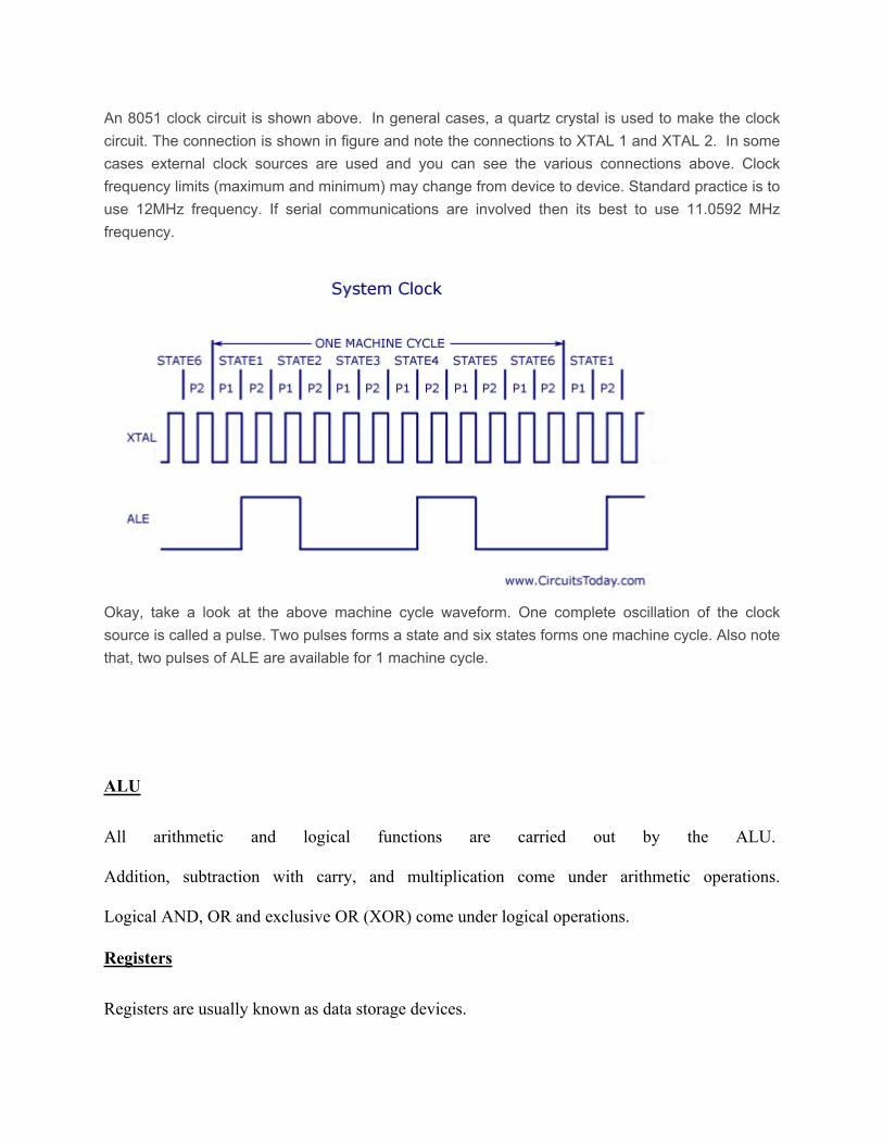
An 8051 clock circuit is shown above. In general cases, a quartz crystal is used to make the clock circuit. The connection is shown in figure and note the connections to XTAL 1 and XTAL 2. In some cases external clock sources are used and you can see the various connections above. Clock frequency limits (maximum and minimum) may change from device to device. Standard practice is to use 12MHz frequency. If serial communications are involved then its best to use 11.0592 MHz frequency.
Okay, take a look at the above machine cycle waveform. One complete oscillation of the clock source is called a pulse. Two pulses forms a state and six states forms one machine cycle. Also note that, two pulses of ALE are available for 1 machine cycle.
ALU
All arithmetic and logical functions are carried out by the ALU.
Addition, subtraction with carry, and multiplication come under arithmetic operations.
Logical AND, OR and exclusive OR (XOR) come under logical operations.
Registers
Registers are usually known as data storage devices.

A & B Registers
8051 microcontroller has 2 registers, namely Register A and Register B. Register A serves as an accumulator while Register B functions as a general purpose register. These registers are used to store the output of mathematical and logical instructions.
The operations of addition, subtraction, multiplication and division are carried out by Register A. Register B is usually unused and comes into picture only when multiplication and division functions are carried out by Register A. Register A also involved in data transfers between the microcontroller and external memory.
Program Counter (PC)
A program counter is a 16-bit register and it has no internal address. The basic function of program counter is to fetch from memory the address of the next instruction to be executed. The PC holds the address of the next instruction residing in memory and when a command is encountered, it produces that instruction. This way the PC increments automatically, holding the address of the next instruction.
Data Pointer (DPTR)
The data pointer or DPTR is a 16-bit register. It is made up of two 8-bit registers called DPH and DPL. Separate addresses are assigned to each of DPH and DPL. These 8-bit registers are used for the storing the memory addresses that can be used to access internal and external data/code.
Stack Pointer (SP)
The stack pointer (SP) in 8051 is an 8-bit register. The main purpose of SP is to access the stack. As it has 8-bits it can take values in the range 00 H to FF H. Stack is a special area of data in memory. The SP acts as a pointer for an address that points to the top of the stack.
PSW (Program Status Word)
Program Status Word or PSW is a hardware register which is a memory location which holds a program's information and also monitors the status of the program this is currently being executed. PSW also has a pointer which points towards the address of the next instruction to be executed. PSW register has 3 fields namely are instruction address field, condition code field and error status field. We can say that PSW is an internal register that keeps track of the computer at every instant.
Generally, the instruction of the result of a program is stored in a single bit register called a 'flag'. The are7 flags in the PSW of 8051. Among these 7 flags, 4 are math flags and 3 are general purpose or user flags.

The 4 Math flags are: Carry flag(C), Auxiliary Carry (AC) ,Overflow (OV) and Parity (P)
The 3 General purpose flags or User flags are: FO, GFO and GF 1
CY PSW.7 Carry flag (Carry out from the D7 bit)
AC PSW.6 Auxiliary carry flag (A carry from D3 to D4)
— PSW.5 Available to the user for general purpose
RS1 PSW.4 Register Bank selector bit 1.
RS0 PSW.3 Register Bank selector bit 0.
OV PSW.2 Overflow flag.
— PSW.1 User definable bit.
P PSW.0 Parity flag. Set/cleared by hardware each instruction cycle to indicate an
odd/even number of 1 bits in the accumulator.
\
Special function registers
The table shows the list of special function registers for various operations in 8051.

Internal RAM and ROM
ROM
A code of 4K memory is incorporated as on-chip ROM in 8051. The 8051 ROM is a non-volatile memory meaning that its contents cannot be altered and hence has a similar range of data and program memory, i.e, they can address program memory as well as a 64K separate block of data memory.

RAM
The 8051 microcontroller is composed of 128 bytes of internal RAM. This is a volatile memory since its contents will be lost if power is switched off. These 128 bytes of internal RAM are divided into 32 working registers which in turn constitute 4 register banks (Bank 0-Bank 3) with each bank consisting of 8 registers (R0 - R7). There are 128 addressable bits in the internal RAM.
Data and Address Bus
A bus is group of wires using which data transfer takes place from one location to another within a system. Buses reduce the number of paths or cables needed to set up connection between components.
There are mainly two kinds of buses - Data Bus and Address Bus
Data Bus: The purpose of data bus is to transfer data. It acts as an electronic channel using which data travels. Wider the width of the bus, greater will be the transmission of data.
Address Bus: The purpose of address bus is to transfer information but not data. The information tells from where within the components, the data should be sent to or received from. The

capacity or memory of the address bus depends on the number of wires that transmit a single address bit.
Four General Purpose Parallel Input/Output Ports
The 8051 microcontroller has four 8-bit input/output ports. These are:
PORT P0: When there is no external memory present, this port acts as a general purpose input/output port. In the presence of external memory, it functions as a multiplexed address and data bus. It performs a dual role.
PORT P1: This port is used for various interfacing activities. This 8-bit port is a normal I/O port i.e. it does not perform dual functions.
PORT P2: Similar to PORT P0, this port can be used as a general purpose port when there is no external memory but when external memory is present it works in conjunction with PORT PO as an address bus. This is an 8-bit port and performs dual functions.
PORT P3: PORT P3 behaves as a dedicated I/O port
PORT 0 :
The structure of a Port-0 pin is shown in fig 6.It has 8 pins (P0.0-P0.7).

Add caption
Port-0 can be used as a normal bidirectional I/O port or it can be used for address/data interfacing for accessing external memory. When control is '1', the port is used for address/data interfacing. When the control is '0', the port can be used as a bidirectional I/O port.
PORT 0 as an Input Port
Let us assume that control is '0'. When the port is used as an input port, '1' is written to the latch. In this situation both the output MOSFETs are 'off'. Hence the output pin have floats hence whatever data written on pin is directly read by read pin.
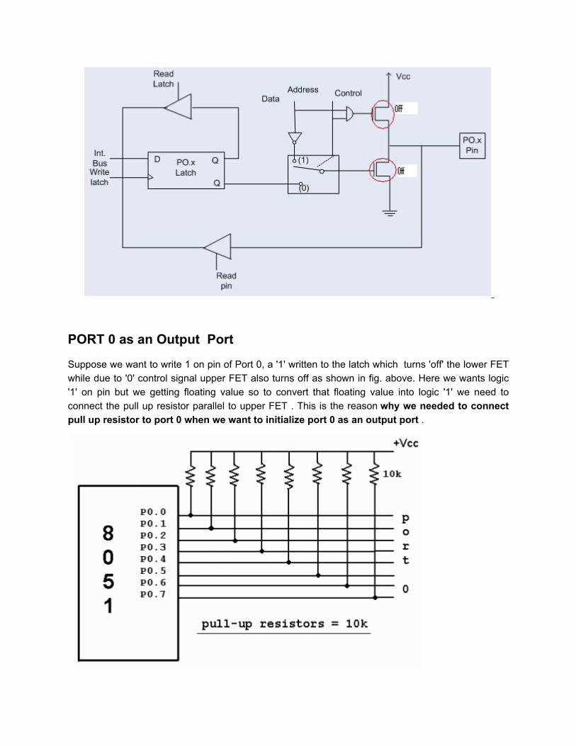
PORT 0 as an Output Port
Suppose we want to write 1 on pin of Port 0, a '1' written to the latch which turns 'off' the lower FET while due to '0' control signal upper FET also turns off as shown in fig. above. Here we wants logic '1' on pin but we getting floating value so to convert that floating value into logic '1' we need to connect the pull up resistor parallel to upper FET . This is the reason why we needed to connect pull up resistor to port 0 when we want to initialize port 0 as an output port .

If we want to write '0' on pin of port 0 , when '0' is written to the latch, the pin is pulled down by the lower FET. Hence the output becomes zero.
When the control is '1', address/data bus controls the output driver FETs. If the address/data bus (internal) is '0', the upper FET is 'off' and the lower FET is 'on'. The output becomes '0'. If the address/data bus is '1', the upper FET is 'on' and the lower FET is 'off'. Hence the output is '1'. Hence for normal address/data interfacing (for external memory access) no pull-up resistors are required.Port-0 latch is written to with 1's when used for external memory access.
PORT 1:
The structure of a port-1 pin is shown in fig below.It has 8 pins (P1.1-P1.7) .

Port-1 dedicated only for I/O interfacing. When used as output port, not needed to connect additional pull-up resistor like port 0. It have provided internally pull-up resistor as shown in fig. below. The pin is pulled up or down through internal pull-up when we want to initialize as an output port. To use port-1 as input port, '1' has to be written to the latch. In this input mode when '1' is written to the pin by the external device then it read fine. But when '0' is written to the pin by the external device then the external source must sink current due to internal pull-up. If the external device is not able to sink the current the pin voltage may rise, leading to a possible wrong reading.
PORT 2:
The structure of a port-2 pin is shown in fig. below. It has 8-pins (P2.0-P2.7) .

Port-2 we use for higher external address byte or a normal input/output port. The I/O operation is similar to Port-1. Port-2 latch remains stable when Port-2 pin are used for external memory access. Here again due to internal pull-up there is limited current driving capability.
PORT 3:Port-3 (P3.0-P3.7) having alternate functions to each pin,The internal structure of a port-3 pin is shown in fig below.

Following are the alternate functions of port 3:
It work as an IO port same like Port 2. only alternate function of port 3 makes its architecture different than other ports.
Timers and Counters
The 8051 has two timers: timer0 and timer1. They can be used either as timers or as counters. Both timers are 16 bits wide. Since the 8051 has an 8-bit architecture, each 16-bit is accessed as two separate registers of low byte and high byte. First we shall discuss about Timer0 registers.
Timer0 registers is a 16 bits register and accessed as low byte and high byte. The low byte is referred as a TL0 and the high byte is referred as TH0. These registers can be accessed like any other registers.
Timer1 registers is also a 16 bits register and is split into two bytes, referred to as TL1 and TH1.

TMOD (timer mode) Register: This is an 8-bit register which is used by both timers 0 and 1 to set the various timer modes. In this TMOD register, lower 4 bits are set aside for timer0 and the upper 4 bits are set aside for timer1. In each case, the lower 2 bits are used to set the timer mode and upper 2 bits to specify the operation.
TMOD
In upper or lower 4 bits, first bit is a GATE bit. Every timer has a means of starting and stopping. Some timers do this by software, some by hardware, and some have both software and hardware controls. The hardware way of starting and stopping the timer by an external source is achieved by making GATE=1 in the TMOD register. And if we change to GATE=0 then we do no need external hardware to start and stop the timers.
The second bit is C/T bit and is used to decide whether a timer is used as a time delay generator or an event counter. If this bit is 0 then it is used as a timer and if it is 1 then it is used as a counter.
In upper or lower 4 bits, the last bits third and fourth are known as M1 and M0 respectively. These are used to select the timer mode.
M0 M1 Mode Operating Mode 0 0 0 13-bit timer mode, 8-bit timer/counter THx and TLx as 5-bit prescalar.
0 1 1 16-bit timer mode, 16-bit timer/counters THx and TLx are cascaded; There are no prescalar.
1 0 2 8-bit auto reload mode, 8-bit auto reload timer/counter; THx holds a value which is to be reloaded into TLx each time it overflows.
1 1 3 Spilt timer mode.
Mode 1- It is a 16-bit timer; therefore it allows values from 0000 to FFFFH to be loaded into the timer’s registers TL and TH. After TH and TL are loaded with a 16-bit initial value, the timer must be started. We can do it by “SETB TR0” for timer 0 and “SETB TR1” for timer 1. After the timer is started. It starts count up until it reaches its limit of FFFFH. When it rolls over from FFFF to 0000H, it sets high a flag bit called TF (timer flag). This timer flag can be monitored. When this timer flag is raised, one option would be stop the timer with the instructions “CLR TR0“ or CLR TR1 for timer 0 and timer 1 respectively. Again, it must be noted that each timer flag TF0 for timer 0 and TF1 for timer1. After the timer reaches its limit and rolls over, in order to repeat the process the registers TH and TL must be reloaded with the original value and TF must be reset to 0.
Mode 1 programmingThe following are the characteristics and operations of mode 1:
1. It is a 16-bit timer; therefore, it allows values of 0000 to FFFFH to be loadedinto the timer’s registers TL and TH.
2. After TH and TL are loaded with a 16-bit initial value, the timer must be started. This is done by “SETB TRO” for Timer 0 and “SETB TR1″ for Timer 1.
3. After the timer is started, it starts to count up. It counts up until it reaches its limit of FFFFH. When it rolls over from FFFFH to 0000, it sets high a flag bit called TF (timer flag). This timer flag can be monitored. When this timer flag is raised, one option would be to stop the timer with the instructions “CLR TRO” or “CLR TR1″, for Timer 0 and Timer 1, respectively. Again, it must be noted that each timer has its own timer flag: TFO for Timer 0, and TF1 for Timer 1.
4. After the timer reaches its limit and rolls over, in order to repeat the process the registers TH and TL must be reloaded with the original value, and TF must be reset to 0.

Steps to program in mode 1To generate a time delay, using the timer’s mode 1, the following steps are taken. To clarify these steps, see Example 9-4.1. Load the TMOD value register indicating which timer (Timer 0 or Timer 1) is
to be used and which timer mode (0 or 1) is selected.1. Load registers TL and TH with initial count values.2. Start the timer.
1. Keep monitoring the timer flag (TF) with the “JNB TFx, target” instruction to see if it is raised. Get out of the loop when TF becomes high.
3. Stop the timer.4. Clear the TF flag for the next round.5. Go back to Step 2 to load TH and TL again.
Mode0- Mode 0 is exactly same like mode 1 except that it is a 13-bit timer instead of 16-bit. The 13-bit counter can hold values between 0000 to 1FFFH in TH-TL. Therefore, when the timer reaches its maximum of 1FFH, it rolls over to 0000, and TF is raised.
Mode 2- It is an 8 bit timer that allows only values of 00 to FFH to be loaded into the timer’s register TH. After TH is loaded with 8 bit value, the 8051 gives a copy of it to TL. Then the timer must be started. It is done by the instruction “SETB TR0” for timer 0 and “SETB TR1” for timer1. This is like mode 1. After timer is started, it starts to count up by incrementing the TL register. It counts up until it reaches its limit of FFH. When it rolls over from FFH to 00. It sets high the TF (timer flag). If we are using timer 0, TF0 goes high; if using TF1 then TF1 is raised. When Tl register rolls from FFH to 00 and TF is set to 1, TL is reloaded automatically with the original value kept by the TH register. To repeat the process, we must simply clear TF and let it go without any need by the programmer to reload the original value. This makes mode 2 auto reload, in contrast in mode 1 in which programmer has to reload TH and TL.
1. Mode 2 programmingThe following are the characteristics and operations of mode 2.

1. It is an 8-bit timer; therefore, it allows only values of 00 to FFH to be loadedinto the timer’s register TH.
2. After TH is loaded with the 8-bit value, the 8051 gives a copy of it to TL. Thenthe timer must be started. This is done by the instruction “SETB TRO” forTimer 0 and “SETB TR11‘ for Timer 1. This is just like mode 1.
3. After the timer is started, it starts to count up by incrementing the TL register.It counts up until it reaches its limit of FFH. When it rolls over from FFH to00, it sets high the TF (timer flag). If we are using Timer 0, TFO goes high; ifwe are using Timer 1, TF1 is raised.
4. When the TL register rolls from FFH to 0 and TF is set to 1, TL is reloaded automatically with the original value kept by the TH register. To repeat the process, we must simply clear TF and let it go without any need by the programmer to reload the original value. This makes mode 2 an auto-reload, in contrast with mode 1 in which the programmer has to reload TH and TL.
It must be emphasized that mode 2 is an 8-bit timer. However, it has an auto-reloading capability. In auto-reload, TH is loaded with the initial count and a copy of it is given to TL. This reloading leaves TH unchanged, still holding a copy of the original value. This mode has many applications, including setting the baud rate in serial communication, as we will see in Chapter 10.Steps to program in mode 2
To generate a time delay using the timer’s mode 2, take the following steps.

1Load the TMOD value register indicating which timer (Timer 0 or Timer 1) isto be used, and select the timer mode (mode 2).
2. Load the TH registers with the initial count value.3. Start the timer.
3.Keep monitoring the timer flag (TF) with the “JNB TFx, target” instruction to see whether it is raised. Get out of the loop when TF goes high.
4. Clear the TF flag.5. Go back to Step 3, since mode 2 is auto-reload.
Mode3- Mode 3 is also known as a split timer mode. Timer 0 and 1 may be programmed to be in mode 0, 1 and 2 independently of similar mode for other timer. This is not true for mode 3; timers do not operate independently if mode 3 is chosen for timer 0. Placing timer 1 in mode 3 causes it to stop counting; the control bit TR1 and the timer 1 flag TF1 are then used by timer0.
TCON register- Bits and symbol and functions of every bits of TCON are as follows:
BIT Symbol Functions 7 TF1 Timer1 over flow flag. Set when timer rolls from all 1s to 0. Cleared
When the processor vectors to execute interrupt service routine
Located at program address 001Bh.
6 TR1 Timer 1 run control bit. Set to 1 by programmer to enable timer to
count; Cleared to 0 by program to halt timer.
5 TF0 Timer 0 over flow flag. Same as TF1.
4 TR0 Timer 0 run control bit. Same as TR1.
3 IE1 External interrupt 1 Edge flag. Not related to timer operations.
2 IT1 External interrupt1 signal type control bit. Set to 1 by program to
Enable external interrupt 1 to be triggered by a falling edge signal. Set
To 0 by program to enable a low level signal on external interrupt1 to
generate an interrupt.
1 IE0 External interrupt 0 Edge flag. Not related to timer operations.
0 IT0 External interrupt 0 signal type control bit. Same as IT0.
Interrupt Control
An event which is used to suspend or halt the normal program execution for a temporary period of time in order to serve the request of another program or hardware device is called an interrupt. An interrupt can either be an internal or external event which suspends the microcontroller for a while and thereby obstructs the sequential flow of a program.
There are two ways of giving interrupts to a microcontroller – one is by sending software instructions and the other is by sending hardware signals. The interrupt mechanism keeps the normal program execution in a "put on hold" mode and executes a subroutine program and after the subroutine is executed, it gets back to its normal program execution. This subroutine program is also called an interrupt handler. A subroutine is executed when a certain event occurs.
These five sources of interrupts in 8051are: ( 1,2 and 5 are internal interrupts . 3 and 4 are external interrupts).
1. Timer 0 overflow interrupt- TF02. Timer 1 overflow interrupt- TF13. External hardware interrupt- INT04. External hardware interrupt- INT15. Serial communication interrupt- RI/TI

The Timer and Serial interrupts are internally generated by the microcontroller, whereas the external interrupts are generated by additional interfacing devices or switches that are externally connected to the microcontroller. These external interrupts can be edge triggered or level triggered. When an interrupt occurs, the microcontroller executes the interrupt service routine so that memory location corresponds to the interrupt that enables it. The Interrupt corresponding to the memory location is given in the interrupt vector table below.
Interrupt Source Vector address Interrupt priority
External Interrupt 0 –INT0
0003H 1
Timer 0 Interrupt
000BH 2
External Interrupt 1 –INT1
0013H 3
Timer 1 Interrupt
001BH 4
Serial Interrupt
0023H 5
Interrupt Enable register
This register is responsible for enabling and disabling the interrupt. It is a bit addressable register in which EA must be set to one for enabling interrupts. The corresponding bit in this register enables particular interrupt like timer, external and serial inputs. In the below IE register, bit corresponding to 1 activates the interrupt and 0 disables the interrupt.

Interrupt priority Register
It is also possible to change the priority levels of the interrupts by setting or clearing the corresponding bit in the Interrupt priority (IP) register as shown in the figure. This allows the low priority interrupt to interrupt the high-priority interrupt, but prohibits the interruption by another low-priority interrupt. Similarly, the high-priority interrupt cannot be interrupted. If these interrupt priorities are not programmed, the microcontroller executes in predefined manner and its order is INT0, TF0, INT1, TF1, and SI.

Serial Data Communication
A method of establishing communication among computers is by transmitting and receiving data bits is a serial connection network. In 8051, the SBUF (Serial Port Data Buffer) register holds the data; the SCON (Serial Control) register manages the data communication and the PCON (Power Control) register manages the data transfer rates. Further, two pins - RXD and TXD, establish the serial network.
The SBUF register has 2 parts – one for storing the data to be transmitted and another for receiving data from outer sources. The first function is done using TXD pin and the second function is done using RXD pin.
SCON Register
There are 4 programmable modes in serial data communication. They are:
1. Serial Data mode 0 (shift register mode) 2. Serial Data mode 1 (standard UART)3. Serial Data mode 2 (multiprocessor mode) 4. Serial Data mode 3
SM0 SM1 Mode/Description/Baud rate
0 0 0,shift register,(Fosc./12)
0 1 1,8 bit UART,Variable
1 0 2,9 bit UART,(Fosc./64) OR (Fosc./32)
1 1 3,9 bit UART, Variable
SMO, SM1SMO and SMI are D7 and D6 of the SCON register, respectively. These two bits determine the framing of data by specifying the number of bits per character, and the start and stop bits. They take the following combinations.

Of the 4 serial modes, only mode I is of interest to us. Further explanation for the other three modes is in Appendix A.2. They are rarely used today. In the SCON register, when serial mode 1 is chosen, the data framing is 8 bits, 1 stop bit, and 1 start bit, which makes it compatible with the COM port of IBM/compatible PCs. More importantly, serial mode 1 allows the baud rate to be variable and is set by Timer 1 of the 8051. In serial mode 1, for each character a total of 10 bits are transferred, where the first bit is the start bit, followed by 8 bits of data, and finally 1 stop bit.SM2SM2 is the D5 bit of the SCON register. This bit enables the multiprocessing capability of the 8051 and is beyond the discussion of this chapter. For our applications, we will make SM2 = 0 since we are not using the 8051 in a multiprocessor environment.RENThe REN (receive enable), bit is D4 of the SCON register. The REN bit is also referred to as SCON.4 since SCON is a bit-addressable register. When the REN bit is high, it allows the 8051 to receive data on the RxD pin of the 8051. As a result if we want the 8051 to both transfer and receive data, REN must be set to 1. By making REN = 0, the receiver is disabled. Making REN — 1 or REN = 0 can
be achieved by the instructions “SETB SCON. 4″ and “CLR SCON. 4″, respectively. Notice that these instructions use the bit-addressable features of register SCON. This bit can be used to block any serial data reception and is an extremely important bit in the SCON register.TBSTBS (transfer bit 8) is bit D3 of SCON. It is used for serial modes 2 and 3. We make TBS = 0 since it is not used in our applications.RB8RB8 (receive bit 8) is bit D2 of the SCON register. In serial mode 1, this bit gets a copy of the stop bit when an 8-bit data is received. This bit (as is the case for TBS) is rarely used anymore. In all our applications we will make RB8 = 0. Like TB8, the RB8 bit is also used in serial modes 2 and 3.Tl

TI (transmit interrupt) is bit Dl of the SCON register. This is an extremely important flag bit in the SCON register. When the 8051 finishes the transfer of the 8-bit character, it raises the TI flag to indicate that it is ready to transfer another byte. The TI bit is raised at the beginning of the stop bit. We will discuss its role further when programming examples of data transmission are given.RlRI (receive interrupt) is the DO bit of the SCON register. This is another extremely important flag bit in the SCON register. When the 8051 receives data serially via RxD, it gets rid of the start and stop bits and places the byte in the SBUF register. Then it raises the RI flag bit to indicate that a byte has been received and should be picked up before it is lost. RI is raised halfway through the stop bit, and we will soon see how this bit is used in programs for receiving data serially.Programming the 8051 to transfer data seriallyIn programming the 8051 to transfer character bytes serially, the following steps must be taken.1. The TMOD register is loaded with the value 20H, indicating the use of Timer
1 in mode 2 (8-bit auto-reload) to set the baud rate.2. The TH1 is loaded with one of the values in Table 10-4 to set the baud rate for
serial data transfer (assuming XTAL = 11.0592 MHz).3. The SCON register is loaded with the value 50H, indicating serial mode 1,
where an 8-bit data is framed with start and stop bits.1. TR1 is set to 1 to start Timer 1.2. TI is cleared by the “CLR TI” instruction.3. The character byte to be transferred serially is written into the SBUF register.
1. The TI flag bit is monitored with the use of the instruction ” JNB TI, xx” tosee if the character has been transferred completely.
4. To transfer the next character, go to Step 5.5. Programming the 8051 to receive data seriallyIn the programming of the 8051 to receive character bytes serially, the following steps must be taken.
1. The TMOD register is loaded with the value 20H, indicating the use of Timer1 in mode 2 (8-bit auto-reload) to set the baud rate.
2. TH1 is loaded with one of the values in Table 10-4 to set the baud rate (assuming XTAL = 11.0592MHz).

3. The SCON register is loaded with the value 50H, indicating serial mode 1,where 8-bit data is framed with start and stop bits and receive enable is turnedon.
6. TR1 is set to 1 to start Timer 1.7. RI is cleared with the “CLR RI” instruction.
1. The RI flag bit is monitored with the use of the instruction “JNB RI, xx” tosee if an entire character has been received yet.
8. When RI is raised, SBUF has the byte. Its contents are moved into a safe place.9. To receive the next character, go to Step 5.
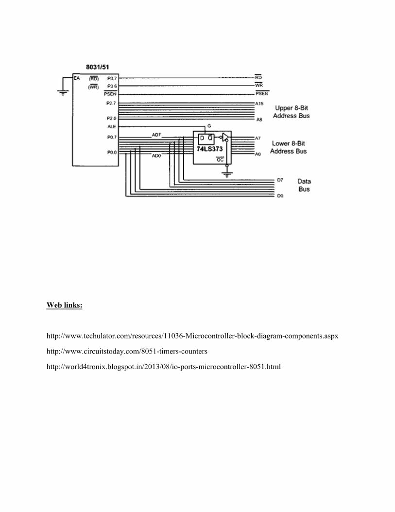
External memory interface with 8051
Address/Data MultiplexingFrom Figure, it is important to note that normally ALE = 0, and PO is used as a data bus, sending data out or bringing data in. Whenever the 8031/51 wants to use PO as an address bus, it puts the addresses AO – A7 on the PO pins and activates ALE = 1 to indicate that PO has the addresses.
PSEN
Another important signal for the 8031/51 is the PSEN (program store enable) signal. PSEN is an output signal for the 8031/51 microcontroller and must be connected to the OE pin of a ROM containing the program code. In other words, to access external ROM containing program code, the 8031/51 uses the PSEN signal. It is important to emphasize the role of EA and PSEN when connecting the 8031/51 to external ROM. When the EA pin is connected to GND, the 8031/51 fetches opcode from external ROM by using PSEN. The connection of the PSEN pin to the OE pin of ROM. In systems based on the 8751/89C51/DS5000 where EA is connected to VCC, these chips do not activate the PSEN pin. This indicates that the on-chip ROM contains program code.In systems where the external ROM contains the program code, burning the program into ROM leaves the microcontroller chip untouched. This is preferable in some applications due to flexibility. In such applications the software is updated via the serial or parallel ports of the IBM PC. This is especially the case during software development and this method is widely used in many 8051-based trainers and emulators.
Web links:
http://www.techulator.com/resources/11036-Microcontroller-block-diagram-components.aspx
http://www.circuitstoday.com/8051-timers-counters
http://world4tronix.blogspot.in/2013/08/io-ports-microcontroller-8051.html