Embed Size (px)
Citation preview
www.unicourse.org Unit Workbook 2 – Level 4 EEE – U71 Combinational & Sequential Logic LO2 Sequential Logic author: Michael Lopez BEng(Hons) MSc PGCert CertEd MIFL MIET FHEA ©UniCourse Ltd 2015
Page 1 of 20
online learning
Pearson BTEC Higher Nationals in Electrical and Electronic Engineering (QCF)
Unit 71: Combinational & Sequential Logic
Unit Workbook 2 in a series of 3 for this unit
Learning Outcome:
Sequential Logic

www.unicourse.org Unit Workbook 2 – Level 4 EEE – U71 Combinational & Sequential Logic LO2 Sequential Logic author: Michael Lopez BEng(Hons) MSc PGCert CertEd MIFL MIET FHEA ©UniCourse Ltd 2015
Page 2 of 20
Contents INTRODUCTION .................................................................................................................................................. 3
GUIDANCE .......................................................................................................................................................... 3
2 Sequential Logic ........................................................................................................................................ 4
2.1 Sequential Logic Devices .................................................................................................................... 4
2.1.1 J-K Flip-Flop ................................................................................................................................. 4
2.1.2 D-type Flip Flop ........................................................................................................................... 5
2.1.3 Monostable ................................................................................................................................. 5
2.1.4 Counter ........................................................................................................................................ 6
2.1.5 Parallel Latch ............................................................................................................................... 8
2.2.6 Shift Register ............................................................................................................................... 9
2.2 Design of Sequential Circuits .............................................................................................................. 9
2.2.1 Minimisation ............................................................................................................................... 9
2.2.2 Race Hazards ............................................................................................................................. 16
2.2.3 Clock Speed ............................................................................................................................... 16
2.2.4 Power Supply Decoupling ......................................................................................................... 17
2.2.5 CMOS Trade-Offs ....................................................................................................................... 17
2.3 Sequential Logic Circuits ................................................................................................................... 17
2.3.1 Clock Generator ........................................................................................................................ 17
2.3.2 BCD Counter .............................................................................................................................. 18
2.3.3 Parallel to Serial Converter ....................................................................................................... 18
2.3.4 Pseudo-Random Number Generator ........................................................................................ 20
2.4 Computer Simulation........................................................................................................................ 20
www.unicourse.org Unit Workbook 2 – Level 4 EEE – U71 Combinational & Sequential Logic LO2 Sequential Logic author: Michael Lopez BEng(Hons) MSc PGCert CertEd MIFL MIET FHEA ©UniCourse Ltd 2015
Page 3 of 20
Purpose
Theory
Question
Challenge
ee
Example
Video
INTRODUCTION This Workbook guides you through the learning outcomes related to:
Sequential logic devices: J-K flip-flop; D-type flip-flop; monostable; counter; parallel latch; shift register
Design sequential circuits: minimisation; race hazards; clock speeds; power supply decoupling; clock
speed/power trade-off for CMOS
Sequential logic circuits: clock generator; BCD counter; parallel to serial converter; pseudo random
number generator
Computer simulation: using a commercial digital electronic circuit analysis package
GUIDANCE This document is prepared to break the unit material down into bite size chunks. You will see the learning
outcomes above treated in their own sections. Therein you will encounter the following structures;
Explains why you need to study the current section of material. Quite often learners
are put off by material which does not initially seem to be relevant to a topic or
profession. Once you understand the importance of new learning or theory you will
embrace the concepts more readily.
Conveys new material to you in a straightforward fashion. To support the treatments
in this section you are strongly advised to follow the given hyperlinks, which may be
useful documents or applications on the web.
The examples/worked examples are presented in a knowledge-building order. Make
sure you follow them all through. If you are feeling confident then you might like to
treat an example as a question, in which case cover it up and have a go yourself.
Many of the examples given resemble assignment questions which will come your
way, so follow them through diligently.
Questions should not be avoided if you are determined to learn. Please do take the
time to tackle each of the given questions, in the order in which they are presented.
The order is important, as further knowledge and confidence is built upon previous
knowledge and confidence. As an Online Learner it is important that the answers to
questions are immediately available to you. You will find the answers, upside down,
below each set of questions. Contact your Unit Tutor if you need help.
You can really cement your new knowledge by undertaking the challenges. A
challenge could be to download software and perform an exercise. An alternative
challenge might involve a practical activity or other form of research.
Videos on the web can be very useful supplements to your distance learning efforts.
Wherever an online video(s) will help you then it will be hyperlinked at the
appropriate point.
www.unicourse.org Unit Workbook 2 – Level 4 EEE – U71 Combinational & Sequential Logic LO2 Sequential Logic author: Michael Lopez BEng(Hons) MSc PGCert CertEd MIFL MIET FHEA ©UniCourse Ltd 2015
Page 4 of 20
2 Sequential Logic
2.1 Sequential Logic Devices
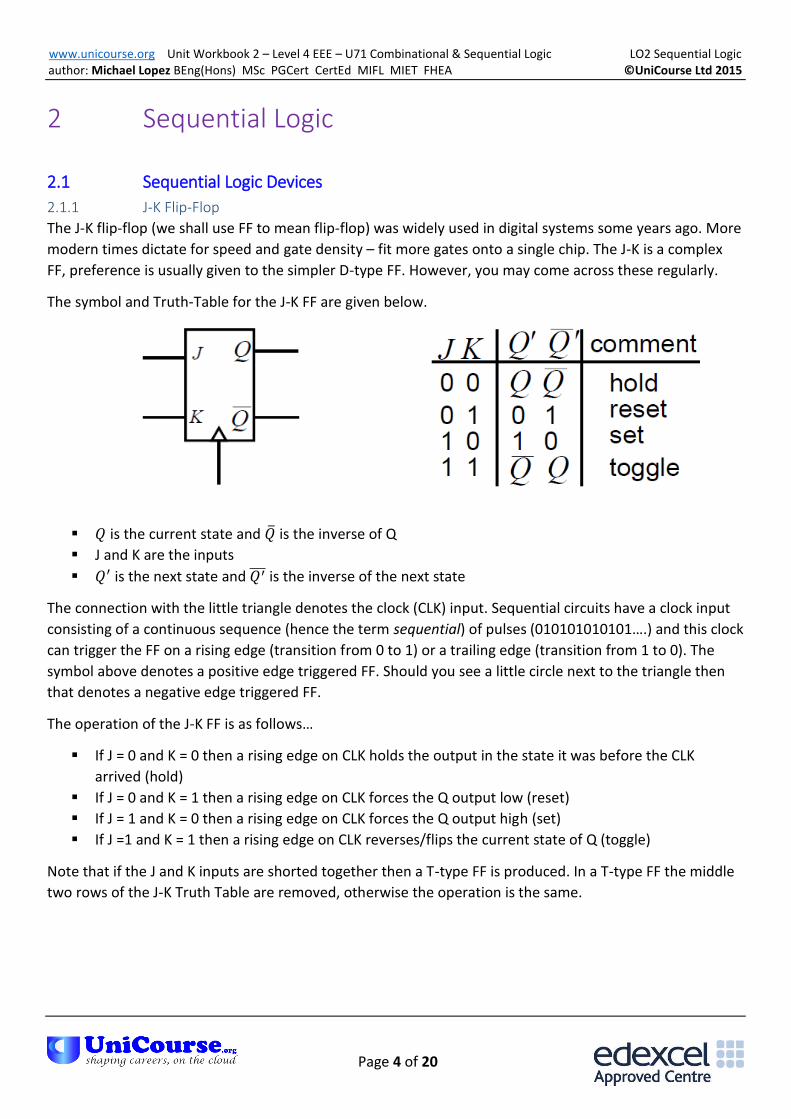
2.1.1 J-K Flip-Flop
The J-K flip-flop (we shall use FF to mean flip-flop) was widely used in digital systems some years ago. More
modern times dictate for speed and gate density – fit more gates onto a single chip. The J-K is a complex
FF, preference is usually given to the simpler D-type FF. However, you may come across these regularly.
The symbol and Truth-Table for the J-K FF are given below.
𝑄 is the current state and �̅� is the inverse of Q
J and K are the inputs
𝑄′ is the next state and 𝑄′̅̅ ̅ is the inverse of the next state
The connection with the little triangle denotes the clock (CLK) input. Sequential circuits have a clock input
consisting of a continuous sequence (hence the term sequential) of pulses (010101010101….) and this clock
can trigger the FF on a rising edge (transition from 0 to 1) or a trailing edge (transition from 1 to 0). The
symbol above denotes a positive edge triggered FF. Should you see a little circle next to the triangle then
that denotes a negative edge triggered FF.
The operation of the J-K FF is as follows…
If J = 0 and K = 0 then a rising edge on CLK holds the output in the state it was before the CLK
arrived (hold)
If J = 0 and K = 1 then a rising edge on CLK forces the Q output low (reset)
If J = 1 and K = 0 then a rising edge on CLK forces the Q output high (set)
If J =1 and K = 1 then a rising edge on CLK reverses/flips the current state of Q (toggle)
Note that if the J and K inputs are shorted together then a T-type FF is produced. In a T-type FF the middle
two rows of the J-K Truth Table are removed, otherwise the operation is the same.
www.unicourse.org Unit Workbook 2 – Level 4 EEE – U71 Combinational & Sequential Logic LO2 Sequential Logic author: Michael Lopez BEng(Hons) MSc PGCert CertEd MIFL MIET FHEA ©UniCourse Ltd 2015
Page 5 of 20
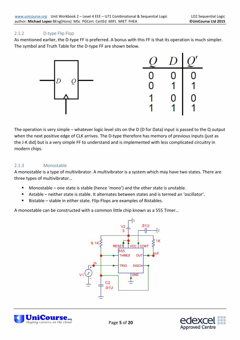
2.1.2 D-type Flip Flop
As mentioned earlier, the D-type FF is preferred. A bonus with this FF is that its operation is much simpler.
The symbol and Truth Table for the D-type FF are shown below.
The operation is very simple – whatever logic level sits on the D (D for Data) input is passed to the Q output
when the next positive edge of CLK arrives. The D-type therefore has memory of previous inputs (just as
the J-K did) but is a very simple FF to understand and is implemented with less complicated circuitry in
modern chips.
2.1.3 Monostable
A monostable is a type of multivibrator. A multivibrator is a system which may have two states. There are
three types of multivibrator…
Monostable – one state is stable (hence ‘mono’) and the other state is unstable.
Astable – neither state is stable. It alternates between states and is termed an ‘oscillator’.
Bistable – stable in either state. Flip-Flops are examples of Bistables.
A monostable can be constructed with a common little chip known as a 555 Timer…
www.unicourse.org Unit Workbook 2 – Level 4 EEE – U71 Combinational & Sequential Logic LO2 Sequential Logic author: Michael Lopez BEng(Hons) MSc PGCert CertEd MIFL MIET FHEA ©UniCourse Ltd 2015
Page 6 of 20
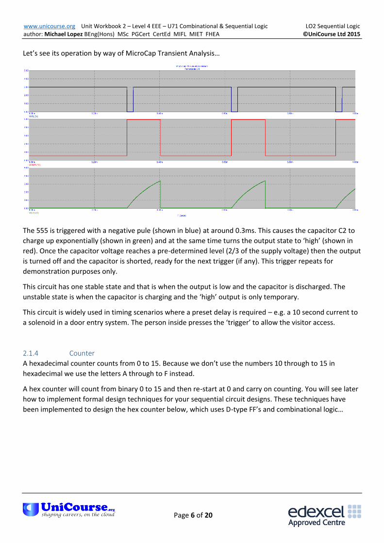
Let’s see its operation by way of MicroCap Transient Analysis…
The 555 is triggered with a negative pule (shown in blue) at around 0.3ms. This causes the capacitor C2 to
charge up exponentially (shown in green) and at the same time turns the output state to ‘high’ (shown in
red). Once the capacitor voltage reaches a pre-determined level (2/3 of the supply voltage) then the output
is turned off and the capacitor is shorted, ready for the next trigger (if any). This trigger repeats for
demonstration purposes only.
This circuit has one stable state and that is when the output is low and the capacitor is discharged. The
unstable state is when the capacitor is charging and the ‘high’ output is only temporary.
This circuit is widely used in timing scenarios where a preset delay is required – e.g. a 10 second current to
a solenoid in a door entry system. The person inside presses the ‘trigger’ to allow the visitor access.
2.1.4 Counter
A hexadecimal counter counts from 0 to 15. Because we don’t use the numbers 10 through to 15 in
hexadecimal we use the letters A through to F instead.
A hex counter will count from binary 0 to 15 and then re-start at 0 and carry on counting. You will see later
how to implement formal design techniques for your sequential circuit designs. These techniques have
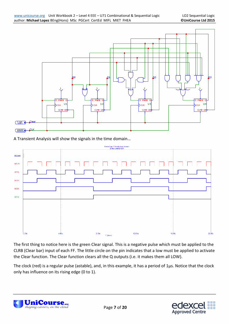
been implemented to design the hex counter below, which uses D-type FF’s and combinational logic…
www.unicourse.org Unit Workbook 2 – Level 4 EEE – U71 Combinational & Sequential Logic LO2 Sequential Logic author: Michael Lopez BEng(Hons) MSc PGCert CertEd MIFL MIET FHEA ©UniCourse Ltd 2015
Page 7 of 20
A Transient Analysis will show the signals in the time domain…
The first thing to notice here is the green Clear signal. This is a negative pulse which must be applied to the
CLRB (Clear bar) input of each FF. The little circle on the pin indicates that a low must be applied to activate
the Clear function. The Clear function clears all the Q outputs (i.e. it makes them all LOW).
The clock (red) is a regular pulse (astable), and, in this example, it has a period of 1µs. Notice that the clock
only has influence on its rising edge (0 to 1).
www.unicourse.org Unit Workbook 2 – Level 4 EEE – U71 Combinational & Sequential Logic LO2 Sequential Logic author: Michael Lopez BEng(Hons) MSc PGCert CertEd MIFL MIET FHEA ©UniCourse Ltd 2015
Page 8 of 20
The signals in blue are the states of the Q0, Q1, Q2 and Q3 FF outputs. To confirm whether this circuit is
counting as we require, take a look at the point where CLK goes high for the first time – the Q0 output has
gone high and the other Q’s remain low. This is a binary representation of the decimal number 1.
Further on in time, take a look at what happens just after the 15th CLK pulse – all the Q’s are high, giving
1111, which is the binary representation of the decimal number 15. Notice also that the 16th pulse sets all
the Q’s back to zero – the circuit starts counting all over again, and will do so until it is turned off.
Don’t worry too much about all that crazy looking combinational logic for the moment. When you
understand the design technique introduced later you will view this combinational logic in a more
favourable light.
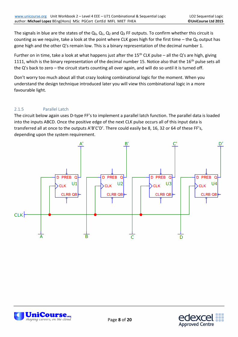
2.1.5 Parallel Latch
The circuit below again uses D-type FF’s to implement a parallel latch function. The parallel data is loaded
into the inputs ABCD. Once the positive edge of the next CLK pulse occurs all of this input data is
transferred all at once to the outputs A’B’C’D’. There could easily be 8, 16, 32 or 64 of these FF’s,
depending upon the system requirement.
www.unicourse.org Unit Workbook 2 – Level 4 EEE – U71 Combinational & Sequential Logic LO2 Sequential Logic author: Michael Lopez BEng(Hons) MSc PGCert CertEd MIFL MIET FHEA ©UniCourse Ltd 2015
Page 9 of 20
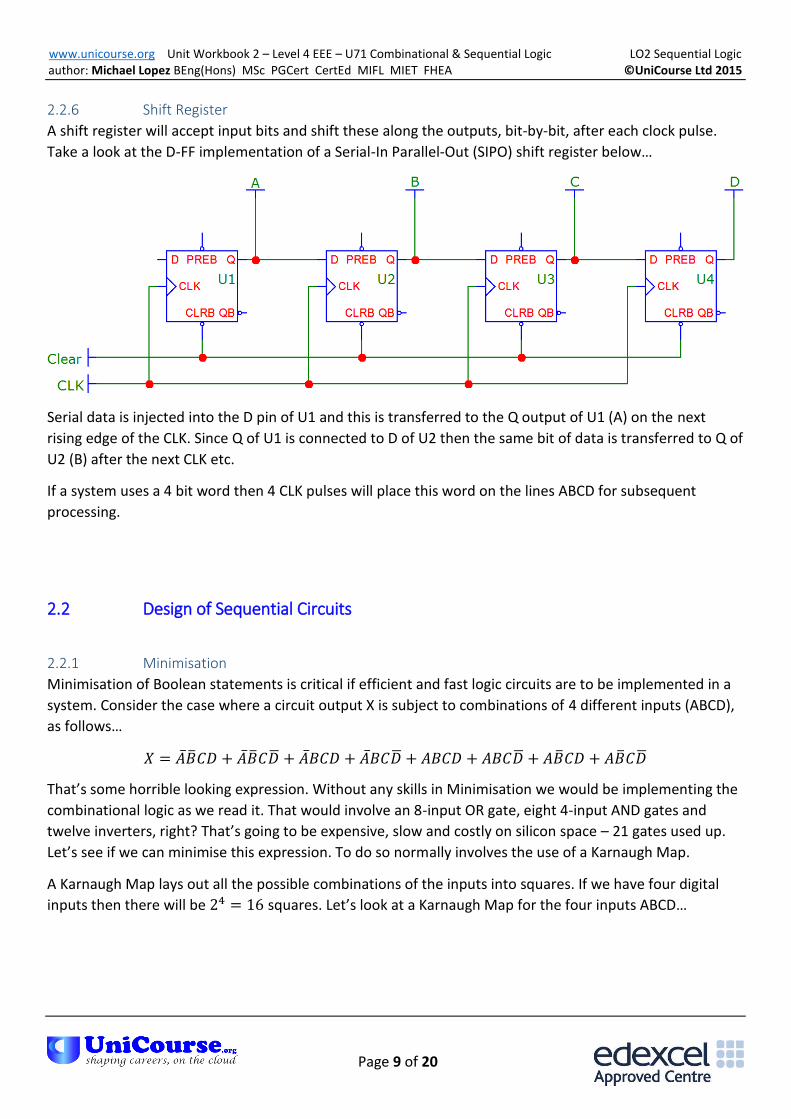
2.2.6 Shift Register
A shift register will accept input bits and shift these along the outputs, bit-by-bit, after each clock pulse.
Take a look at the D-FF implementation of a Serial-In Parallel-Out (SIPO) shift register below…
Serial data is injected into the D pin of U1 and this is transferred to the Q output of U1 (A) on the next
rising edge of the CLK. Since Q of U1 is connected to D of U2 then the same bit of data is transferred to Q of
U2 (B) after the next CLK etc.
If a system uses a 4 bit word then 4 CLK pulses will place this word on the lines ABCD for subsequent
processing.
2.2 Design of Sequential Circuits
2.2.1 Minimisation
Minimisation of Boolean statements is critical if efficient and fast logic circuits are to be implemented in a
system. Consider the case where a circuit output X is subject to combinations of 4 different inputs (ABCD),
as follows…
𝑋 = �̅��̅�𝐶𝐷 + �̅��̅�𝐶�̅� + �̅�𝐵𝐶𝐷 + �̅�𝐵𝐶�̅� + 𝐴𝐵𝐶𝐷 + 𝐴𝐵𝐶�̅� + 𝐴�̅�𝐶𝐷 + 𝐴�̅�𝐶�̅�
That’s some horrible looking expression. Without any skills in Minimisation we would be implementing the
combinational logic as we read it. That would involve an 8-input OR gate, eight 4-input AND gates and
twelve inverters, right? That’s going to be expensive, slow and costly on silicon space – 21 gates used up.
Let’s see if we can minimise this expression. To do so normally involves the use of a Karnaugh Map.
A Karnaugh Map lays out all the possible combinations of the inputs into squares. If we have four digital
inputs then there will be 24 = 16 squares. Let’s look at a Karnaugh Map for the four inputs ABCD…

www.unicourse.org Unit Workbook 2 – Level 4 EEE – U71 Combinational & Sequential Logic LO2 Sequential Logic author: Michael Lopez BEng(Hons) MSc PGCert CertEd MIFL MIET FHEA ©UniCourse Ltd 2015
Page 10 of 20
Worked Example 1
The Karnaugh Map marks the possible logic levels for each pair of signals in the form of a Gray Code. A
Gray Code only allows one input to change at any one time, so we mark as 00, 01, 11, 10 rather than 00,
01, 10, 11 because going from 01 to 10 involves two changes at the same time, which is illegal if we wish to
minimise efficiently.
The eight terms in our expression for X are marked with 1’s on the Karnaugh Map, as shown. Minimisation
involves grouping terms in 2’s, 4’s or 8’s. The terms in this example all form a nice group of eight, as
indicated in red. Looking above the red highlighted area we see that what’s in common with all of those
terms is when C is 1. The startling fact which hits us here is that…
We don’t need 21 gates, we just need to connect X to C
You will see more examples of minimisation using Karnaugh Maps by using formal design techniques, as
demonstrated in the following worked example.
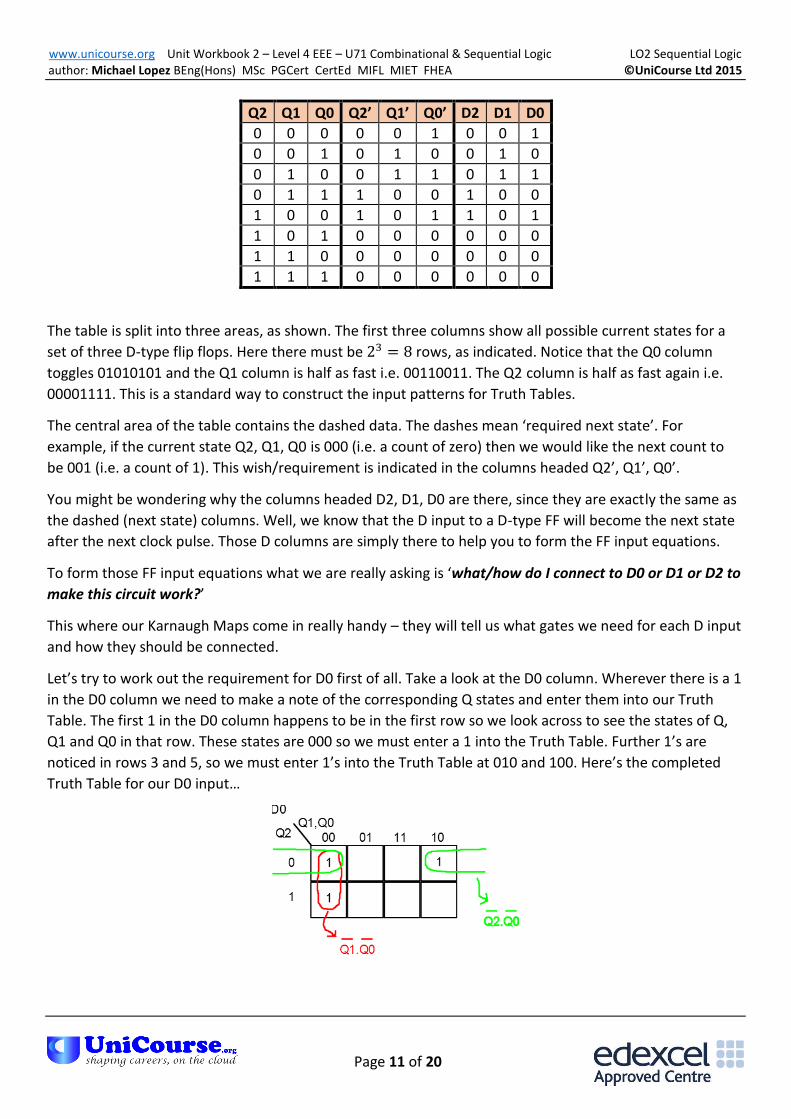
Use formal design techniques to produce the D-Type flip-flop equations for a 0 to 5 Up-Counter.
Our formal design technique firstly requires writing the specification for the system in the form of a
Modified State Transition Table. This table lists all possible present states and the desirable next states to
achieve our specification. Here’s the Modified State Transition Table for our example…
www.unicourse.org Unit Workbook 2 – Level 4 EEE – U71 Combinational & Sequential Logic LO2 Sequential Logic author: Michael Lopez BEng(Hons) MSc PGCert CertEd MIFL MIET FHEA ©UniCourse Ltd 2015
Page 11 of 20
Q2 Q1 Q0 Q2’ Q1’ Q0’ D2 D1 D0
0 0 0 0 0 1 0 0 1
0 0 1 0 1 0 0 1 0
0 1 0 0 1 1 0 1 1
0 1 1 1 0 0 1 0 0
1 0 0 1 0 1 1 0 1
1 0 1 0 0 0 0 0 0
1 1 0 0 0 0 0 0 0
1 1 1 0 0 0 0 0 0
The table is split into three areas, as shown. The first three columns show all possible current states for a
set of three D-type flip flops. Here there must be 23 = 8 rows, as indicated. Notice that the Q0 column
toggles 01010101 and the Q1 column is half as fast i.e. 00110011. The Q2 column is half as fast again i.e.
00001111. This is a standard way to construct the input patterns for Truth Tables.
The central area of the table contains the dashed data. The dashes mean ‘required next state’. For
example, if the current state Q2, Q1, Q0 is 000 (i.e. a count of zero) then we would like the next count to
be 001 (i.e. a count of 1). This wish/requirement is indicated in the columns headed Q2’, Q1’, Q0’.
You might be wondering why the columns headed D2, D1, D0 are there, since they are exactly the same as
the dashed (next state) columns. Well, we know that the D input to a D-type FF will become the next state
after the next clock pulse. Those D columns are simply there to help you to form the FF input equations.
To form those FF input equations what we are really asking is ‘what/how do I connect to D0 or D1 or D2 to
make this circuit work?’
This where our Karnaugh Maps come in really handy – they will tell us what gates we need for each D input
and how they should be connected.
Let’s try to work out the requirement for D0 first of all. Take a look at the D0 column. Wherever there is a 1
in the D0 column we need to make a note of the corresponding Q states and enter them into our Truth
Table. The first 1 in the D0 column happens to be in the first row so we look across to see the states of Q,
Q1 and Q0 in that row. These states are 000 so we must enter a 1 into the Truth Table. Further 1’s are
noticed in rows 3 and 5, so we must enter 1’s into the Truth Table at 010 and 100. Here’s the completed
Truth Table for our D0 input…

www.unicourse.org Unit Workbook 2 – Level 4 EEE – U71 Combinational & Sequential Logic LO2 Sequential Logic author: Michael Lopez BEng(Hons) MSc PGCert CertEd MIFL MIET FHEA ©UniCourse Ltd 2015
Page 12 of 20
Those three 1’s have been entered. We now try to group the data in 2’s, 4’s or 8’s, where possible. The two
1’s highlighted in red both lie in the column where Q1 and Q0 are both 0. We also notice for the red group
that Q2 can be either 0 or 1. We always try to look for common states in Truth Tables, so we ignore Q2
altogether and record this red group as Q1 being 0 and Q0 being 0 i.e. 𝑄1̅̅ ̅̅ . 𝑄0̅̅ ̅̅ is the term in red.
We now need to turn our attention to the solitary 1 over on the right hand side of the Truth Table. It would
be very bad practice to call this 𝑄2̅̅ ̅̅ . 𝑄1. 𝑄0̅̅ ̅̅ . It would still be valid and produce a working circuit, but that
circuit would be wasteful of gates and slower than it need to be. We need to remember that we’re in the
business of grouping when we analyse our Karnaugh Maps. If we were to get some scissors and cut out the
Karnaugh Map we could then fold the left edge of the paper and the right edge of the paper to form a
tube. Having made the tube we see that the 1 we are looking at is not solitary after all – it’s next to the 1 in
the top left hand corner. This fact is highlighted by the green grouping in the diagram. For this green
grouping we see that what’s common is Q2 being 0 and Q0 being 0 i.e. 𝑄2̅̅ ̅̅ . 𝑄0̅̅ ̅̅ is the term in green.
We have now minimised the equation for D0 and this can finally be expressed as…
𝑫𝟎 = 𝑸𝟏̅̅ ̅̅ . 𝑸𝟎̅̅ ̅̅ + 𝑸𝟐̅̅ ̅̅ . 𝑸𝟎̅̅ ̅̅
To connect the groups to form the full expression for D0 we must use an OR gate, indicated by the ‘+’ sign
above.
That’s all there is really for minimisation with Karnaugh Maps. The only other thing to remember is that
when you cut out the Karnaugh map you could just as easily have connected to top and bottom edges to
form groups also – that task is not needed in this example though.
One final thought: If you are analysing a Karnaugh Map and you cannot see any groupings then no
minimisation is possible and you must represent each 1 in its full form. This is something you come across
when trying to find the input equations for D1 and D2, which are…
𝑫𝟏 = 𝑸𝟐̅̅ ̅̅ . 𝑸𝟏̅̅ ̅̅ . 𝑸𝟎 + 𝑸𝟐̅̅ ̅̅ . 𝑸𝟏.𝑸𝟎̅̅ ̅̅
𝑫𝟐 = 𝑸𝟐.𝑸𝟏̅̅ ̅̅ . 𝑸𝟎̅̅ ̅̅ + 𝑸𝟐̅̅ ̅̅ . 𝑸𝟏.𝑸𝟎
These equations for the D inputs may be turned into combinational logic gates and the whole circuit may
be constructed in MicroCap as follows…
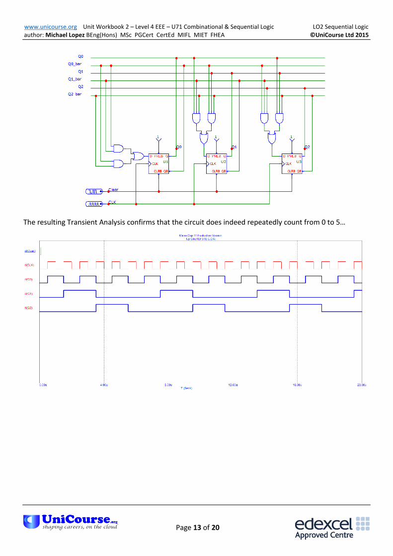
www.unicourse.org Unit Workbook 2 – Level 4 EEE – U71 Combinational & Sequential Logic LO2 Sequential Logic author: Michael Lopez BEng(Hons) MSc PGCert CertEd MIFL MIET FHEA ©UniCourse Ltd 2015
Page 13 of 20
The resulting Transient Analysis confirms that the circuit does indeed repeatedly count from 0 to 5…
www.unicourse.org Unit Workbook 2 – Level 4 EEE – U71 Combinational & Sequential Logic LO2 Sequential Logic author: Michael Lopez BEng(Hons) MSc PGCert CertEd MIFL MIET FHEA ©UniCourse Ltd 2015
Page 14 of 20
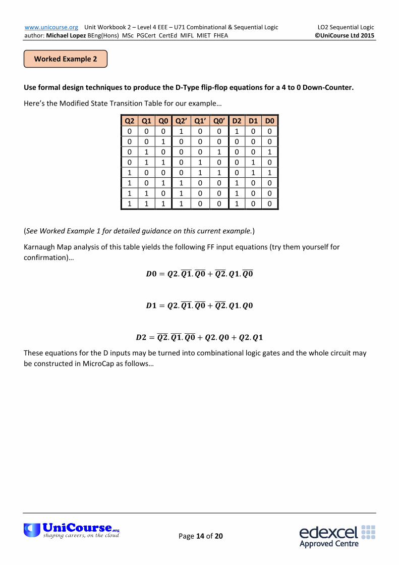
Worked Example 2
Use formal design techniques to produce the D-Type flip-flop equations for a 4 to 0 Down-Counter.
Here’s the Modified State Transition Table for our example…
Q2 Q1 Q0 Q2’ Q1’ Q0’ D2 D1 D0
0 0 0 1 0 0 1 0 0
0 0 1 0 0 0 0 0 0
0 1 0 0 0 1 0 0 1
0 1 1 0 1 0 0 1 0
1 0 0 0 1 1 0 1 1
1 0 1 1 0 0 1 0 0
1 1 0 1 0 0 1 0 0
1 1 1 1 0 0 1 0 0
(See Worked Example 1 for detailed guidance on this current example.)
Karnaugh Map analysis of this table yields the following FF input equations (try them yourself for
confirmation)…
𝑫𝟎 = 𝑸𝟐.𝑸𝟏̅̅ ̅̅ . 𝑸𝟎̅̅ ̅̅ + 𝑸𝟐̅̅ ̅̅ . 𝑸𝟏.𝑸𝟎̅̅ ̅̅
𝑫𝟏 = 𝑸𝟐.𝑸𝟏̅̅ ̅̅ . 𝑸𝟎̅̅ ̅̅ + 𝑸𝟐̅̅ ̅̅ . 𝑸𝟏.𝑸𝟎
𝑫𝟐 = 𝑸𝟐̅̅ ̅̅ . 𝑸𝟏̅̅ ̅̅ . 𝑸𝟎̅̅ ̅̅ + 𝑸𝟐.𝑸𝟎 + 𝑸𝟐.𝑸𝟏
These equations for the D inputs may be turned into combinational logic gates and the whole circuit may
be constructed in MicroCap as follows…
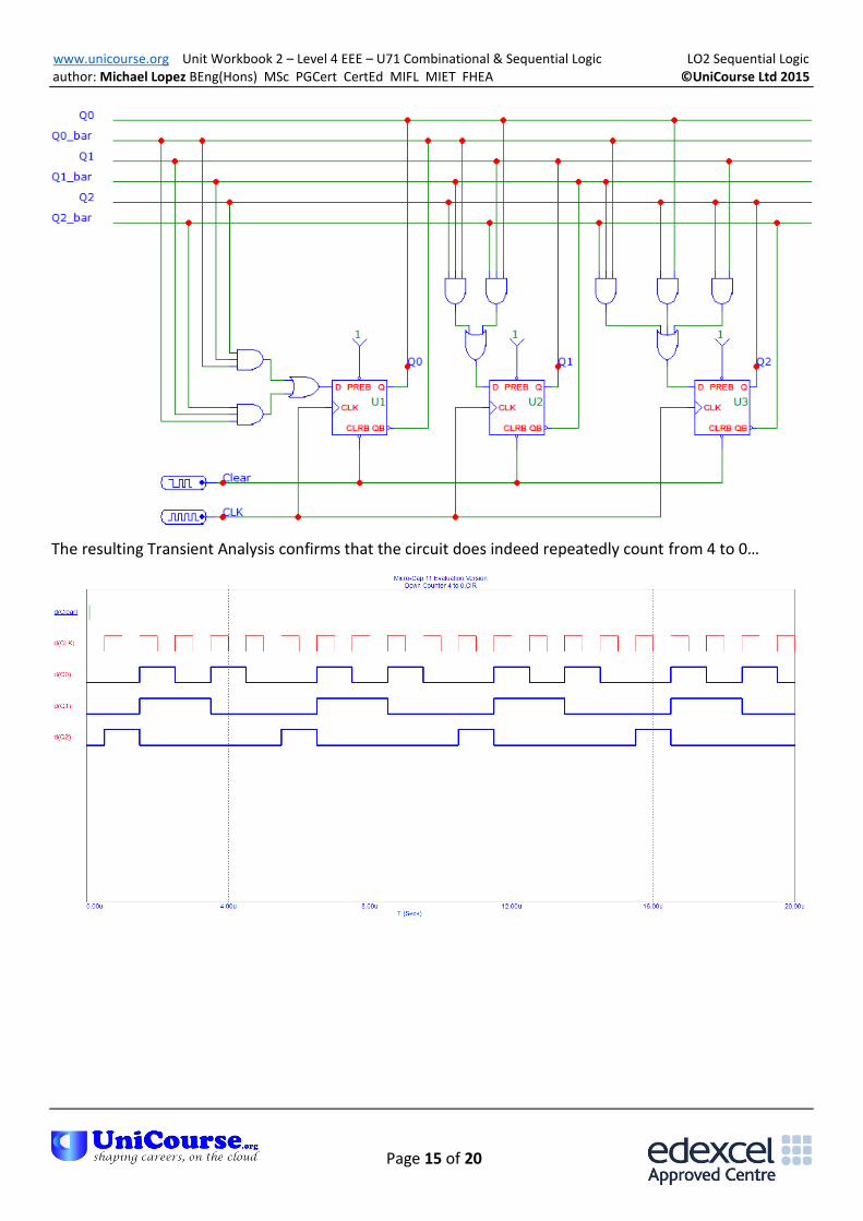
www.unicourse.org Unit Workbook 2 – Level 4 EEE – U71 Combinational & Sequential Logic LO2 Sequential Logic author: Michael Lopez BEng(Hons) MSc PGCert CertEd MIFL MIET FHEA ©UniCourse Ltd 2015
Page 15 of 20
The resulting Transient Analysis confirms that the circuit does indeed repeatedly count from 4 to 0…
www.unicourse.org Unit Workbook 2 – Level 4 EEE – U71 Combinational & Sequential Logic LO2 Sequential Logic author: Michael Lopez BEng(Hons) MSc PGCert CertEd MIFL MIET FHEA ©UniCourse Ltd 2015
Page 16 of 20
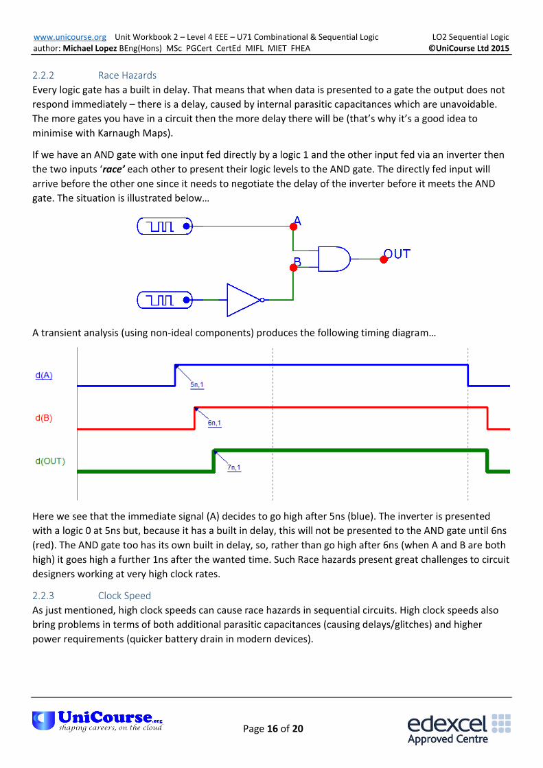
2.2.2 Race Hazards
Every logic gate has a built in delay. That means that when data is presented to a gate the output does not
respond immediately – there is a delay, caused by internal parasitic capacitances which are unavoidable.
The more gates you have in a circuit then the more delay there will be (that’s why it’s a good idea to
minimise with Karnaugh Maps).
If we have an AND gate with one input fed directly by a logic 1 and the other input fed via an inverter then
the two inputs ‘race’ each other to present their logic levels to the AND gate. The directly fed input will
arrive before the other one since it needs to negotiate the delay of the inverter before it meets the AND
gate. The situation is illustrated below…
A transient analysis (using non-ideal components) produces the following timing diagram…
Here we see that the immediate signal (A) decides to go high after 5ns (blue). The inverter is presented
with a logic 0 at 5ns but, because it has a built in delay, this will not be presented to the AND gate until 6ns
(red). The AND gate too has its own built in delay, so, rather than go high after 6ns (when A and B are both
high) it goes high a further 1ns after the wanted time. Such Race hazards present great challenges to circuit
designers working at very high clock rates.
2.2.3 Clock Speed
As just mentioned, high clock speeds can cause race hazards in sequential circuits. High clock speeds also
bring problems in terms of both additional parasitic capacitances (causing delays/glitches) and higher
power requirements (quicker battery drain in modern devices).
www.unicourse.org Unit Workbook 2 – Level 4 EEE – U71 Combinational & Sequential Logic LO2 Sequential Logic author: Michael Lopez BEng(Hons) MSc PGCert CertEd MIFL MIET FHEA ©UniCourse Ltd 2015
Page 17 of 20
2.2.4 Power Supply Decoupling
In logic circuits we must be careful not to expect the power supply to be perfectly smooth. This is not
possible in practice and there are low and high frequency components in the power rail which can cause
glitches in our digital logic. The following two tips are useful for power supply decoupling…
Use a 100µF capacitor to decouple the power rail to ground. This capacitor will usually be of the
electrolytic type and is good at filtering out low frequency noise from the power system.
Use a 100nF ceramic capacitor on each logic chip to filter out high frequency noise. For example, a
74LS00 TTL chip has four 2-input NAND gates on board. That’s fine, just connect a 100nF capacitor
between its power pins (pins 14 and 7). Ensure that the capacitor is as close to the chip as possible
to minimise the copper track length between the two (copper track acts as an aerial – we don’t
need any unwanted transmissions or pick-ups).
2.2.5 CMOS Trade-Offs
As we increase the clock rate we see a much higher power demand from CMOS circuits than we do for TTL
circuits. To reduce the power consumption of CMOS devices at high clock rates the usual strategy is to use
ever decreasing physical sizes for the CMOS transistors. We are now reaching a limit on the smallest
transistors due to physical effects. Designers must be aware of the trade-off needed in terms of high clock
rates and power dissipation.
2.3 Sequential Logic Circuits
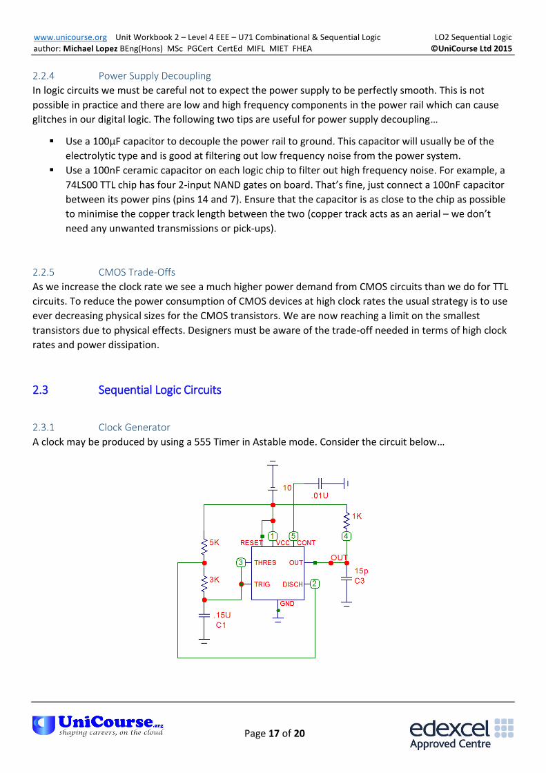
2.3.1 Clock Generator
A clock may be produced by using a 555 Timer in Astable mode. Consider the circuit below…
www.unicourse.org Unit Workbook 2 – Level 4 EEE – U71 Combinational & Sequential Logic LO2 Sequential Logic author: Michael Lopez BEng(Hons) MSc PGCert CertEd MIFL MIET FHEA ©UniCourse Ltd 2015
Page 18 of 20
The important components in this circuit are on the left. The 5k plus the 3k resistors form 8k and this is in
series with the 0.15µF capacitor. These form the timing circuit and the time the output spends high is given
by 0.693 × (5𝑘 + 3𝑘) × 0.15µ𝐹 = 832µ𝑠. The time the circuit spends low is given by 0.693 × 3𝑘 ×
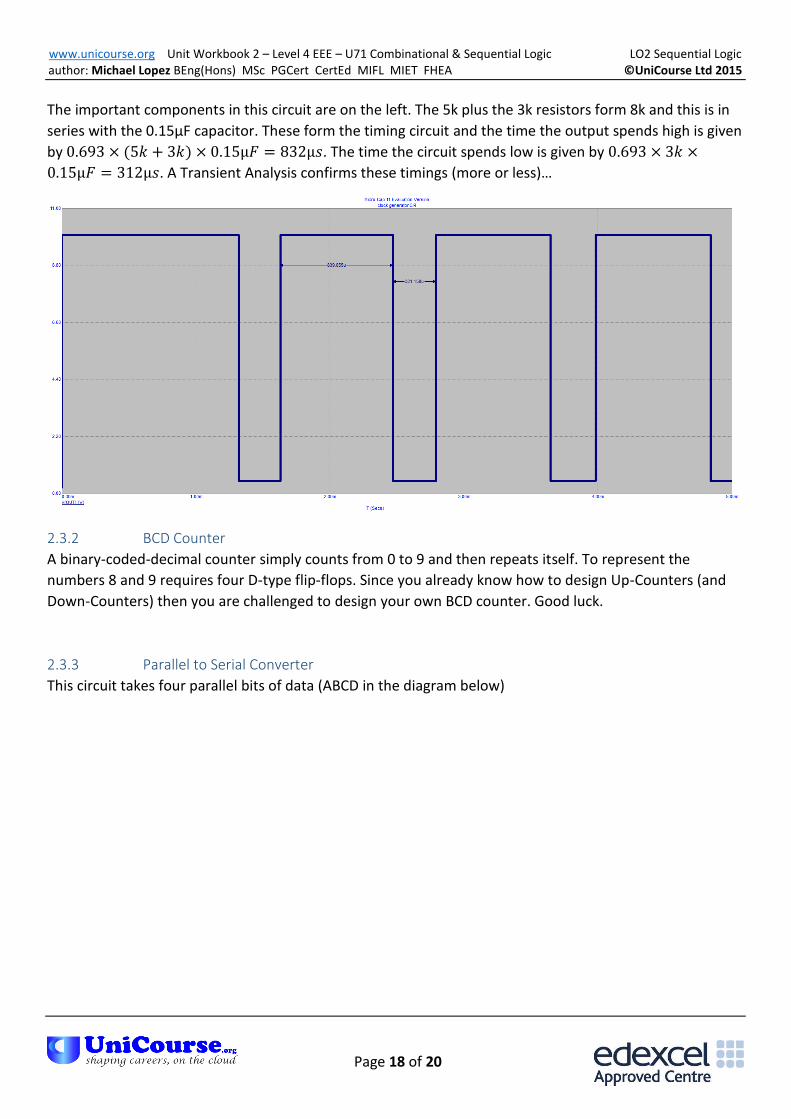
0.15µ𝐹 = 312µ𝑠. A Transient Analysis confirms these timings (more or less)…
2.3.2 BCD Counter
A binary-coded-decimal counter simply counts from 0 to 9 and then repeats itself. To represent the
numbers 8 and 9 requires four D-type flip-flops. Since you already know how to design Up-Counters (and
Down-Counters) then you are challenged to design your own BCD counter. Good luck.
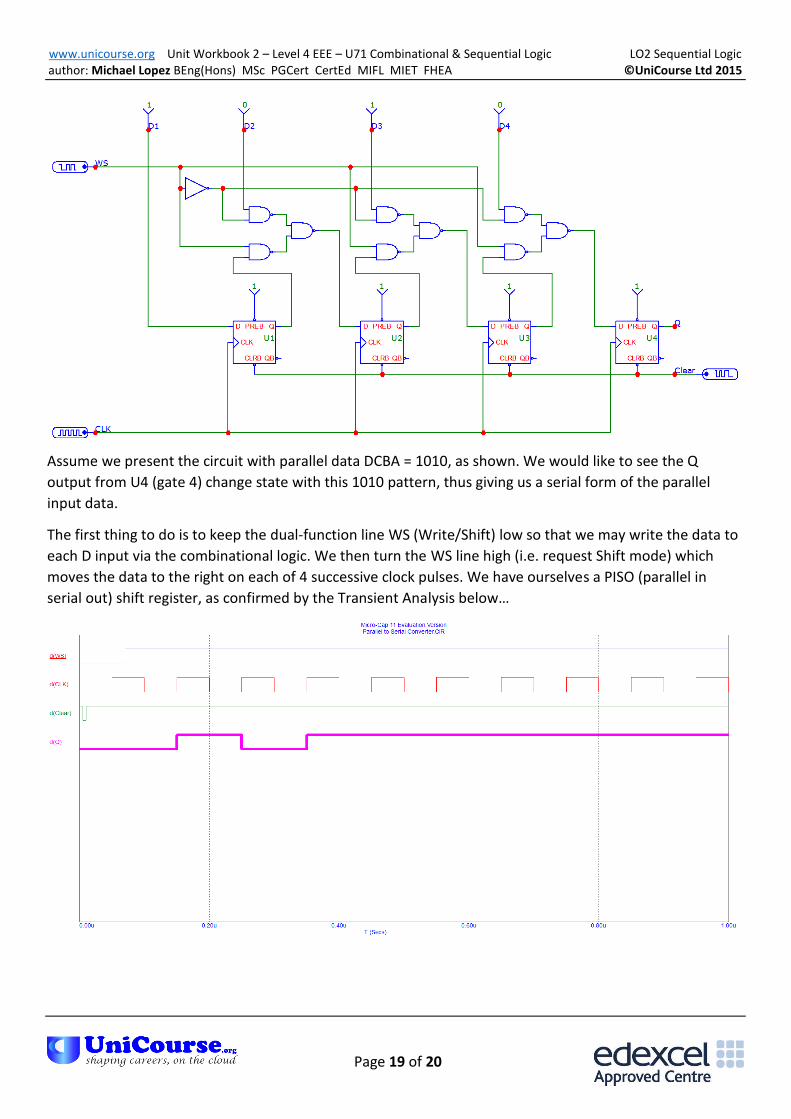
2.3.3 Parallel to Serial Converter
This circuit takes four parallel bits of data (ABCD in the diagram below)
www.unicourse.org Unit Workbook 2 – Level 4 EEE – U71 Combinational & Sequential Logic LO2 Sequential Logic author: Michael Lopez BEng(Hons) MSc PGCert CertEd MIFL MIET FHEA ©UniCourse Ltd 2015
Page 19 of 20
Assume we present the circuit with parallel data DCBA = 1010, as shown. We would like to see the Q
output from U4 (gate 4) change state with this 1010 pattern, thus giving us a serial form of the parallel
input data.
The first thing to do is to keep the dual-function line WS (Write/Shift) low so that we may write the data to
each D input via the combinational logic. We then turn the WS line high (i.e. request Shift mode) which
moves the data to the right on each of 4 successive clock pulses. We have ourselves a PISO (parallel in
serial out) shift register, as confirmed by the Transient Analysis below…
www.unicourse.org Unit Workbook 2 – Level 4 EEE – U71 Combinational & Sequential Logic LO2 Sequential Logic author: Michael Lopez BEng(Hons) MSc PGCert CertEd MIFL MIET FHEA ©UniCourse Ltd 2015
Page 20 of 20
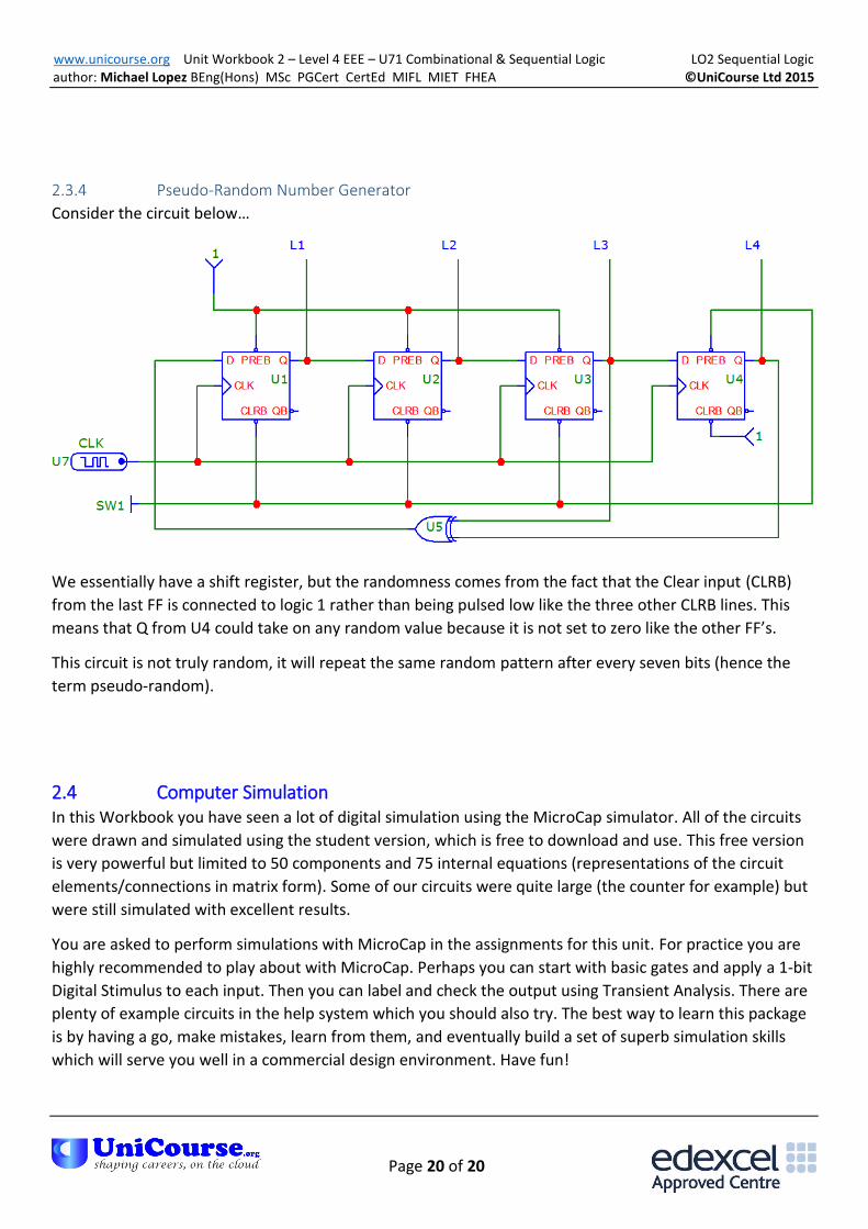
2.3.4 Pseudo-Random Number Generator
Consider the circuit below…
We essentially have a shift register, but the randomness comes from the fact that the Clear input (CLRB)
from the last FF is connected to logic 1 rather than being pulsed low like the three other CLRB lines. This
means that Q from U4 could take on any random value because it is not set to zero like the other FF’s.
This circuit is not truly random, it will repeat the same random pattern after every seven bits (hence the
term pseudo-random).
2.4 Computer Simulation In this Workbook you have seen a lot of digital simulation using the MicroCap simulator. All of the circuits
were drawn and simulated using the student version, which is free to download and use. This free version
is very powerful but limited to 50 components and 75 internal equations (representations of the circuit
elements/connections in matrix form). Some of our circuits were quite large (the counter for example) but
were still simulated with excellent results.
You are asked to perform simulations with MicroCap in the assignments for this unit. For practice you are
highly recommended to play about with MicroCap. Perhaps you can start with basic gates and apply a 1-bit
Digital Stimulus to each input. Then you can label and check the output using Transient Analysis. There are
plenty of example circuits in the help system which you should also try. The best way to learn this package
is by having a go, make mistakes, learn from them, and eventually build a set of superb simulation skills
which will serve you well in a commercial design environment. Have fun!