Embed Size (px)
Citation preview

Unconventional Nanocomputing with Physical Wave Interference Functions Santosh Khasanvis, Mostafizur Rahman, Prasad Shabadi, and C. Andras Moritz1
1
Table of contents
1 Overview __________________________________________________________________________________ 2
2 Spin Waves Physical Layer for WIF Implementation _____________________________ 3
2.1 Physical Fabric Components _________________________________________________________ 4
3 Elementary WIF Operators for Logic ________________________________________________ 7
4 Binary WIF Logic Design _____________________________________________________________ 11
4.1 Binary WIF Full Adder ______________________________________________________________ 12
4.2 Parallel Counters ____________________________________________________________________ 14
4.3 Benchmarking Binary WIF Circuits vs. CMOS ___________________________________ 16
4.4 WIF Topology Exploration _________________________________________________________ 17
5 Multi-valued WIF Logic Design _____________________________________________________ 19
5.1 Multi-valued Operators and Implementation using WIF ______________________ 20
5.2 Multi-valued Arithmetic Circuit Example: Quaternary Full Adder __________ 23
5.3 Benchmarking of WIF Multi-valued Circuits vs. Conventional CMOS ________ 24
5.4 Input/Output Logic for Data Conversion Between Binary and Radix-r
Domains________________________________________________________________________________________ 25
6 Microprocessors with WIF: Opportunities and Challenges ____________________ 26
7 Summary and Future Work _________________________________________________________ 30

Unconventional Nanocomputing with Physical Wave Interference Functions Santosh Khasanvis, Mostafizur Rahman, Prasad Shabadi, and C. Andras Moritz1
2
1 Overview
Growth in the integrated circuit (IC) industry has been primarily driven by CMOS technology
scaling over the past few decades. This scaling trend is fast approaching its fundamental limits,
forcing researchers to look for alternative avenues to build integrated circuits. In this chapter, we
present a new computational paradigm that uses wave physical phenomenon for post-CMOS
nanoscale integrated circuits, called Wave Interference Functions (WIF). The vision here is to use
physical functional elements that are more sophisticated than switches as the building blocks, to
realize complex logic/arithmetic in a single step natively (see Figure 1 for comparison with
Boolean switch). This is in stark contrast to other research efforts that aim to develop faster 3-
terminal switching devices with new nanomaterials and alternate state variables [2]- [10] to
replace traditional transistors (MOSFETs), while retaining the conventional Boolean
computational paradigm. By the time functional blocks are composed, these latter approaches
result in complex networks of logic gates with significant wiring requirements that impact delay,
area, and power consumption. The original goal of having a faster switch becomes less critical,
since system-level performance does not scale in proportion to the individual device performance.
Clearly, a new mindset is necessary to build game-changing computational systems for post-
CMOS integrated circuits, where physical properties are harnessed as they exist vs. remapped to a
Boolean framework.
Wave Interference Functions (WIF) is a multi-valued computation framework where information
is encoded in a combination of wave attributes – amplitude and phase. Wave encoding of data is
multi-dimensional: i.e., each of the wave attributes can take multiple values, and when used in
conjunction they present a plethora of options for multi-valued data encoding intrinsically.
Information processing is achieved through wave superposition interactions called Interference
Functions, and wave propagation, both of which can affect wave phase and amplitude. The output
wave encodes the result as well as information about the inputs in a compressed manner using
both its phase and amplitude. Multi-valued computation with WIF results in a much simpler and
compact network of functions, and multi-valued wave communication reduces interconnection
requirements among these functions when compared to Boolean logic. The resulting WIF
1S. Khasanvis, M. Rahman and C. A. Moritz are with University of Massachusetts Amherst. P. Shabadi is with Marvell
Semiconductors; the work reported here was performed during his graduate study at UMass Amherst.
2This project was supported by DARPA program on Non-volatile Logic, and Center for Hierarchical Manufacturing
(CHM, NSF DMI-0531171) at UMass Amherst.
Figure 1. (Left) Conventional elementary functional element (i.e., binary switch). (Right) Envisioned elementary
functional element for post-CMOS Wave Interference Functions computation paradigm. Here, the elementary
block performs more sophisticated function than a simple switch, operating on large number of multi-valued
multi-dimensional inputs (information in wave phase and amplitude) simultaneously.

3
physical implementations potentially require much smaller area compared to equivalent Boolean
CMOS implementation. Compact circuit implementations may lead to performance benefits as
well. Arbitrary computation can be synthesized based on these functions in a generic and
systematic manner, similar to Boolean logic frameworks.
We illustrate the WIF framework using spin wave physical phenomenon in this chapter. But the
ideas presented here are generic and broadly applicable to any physical phenomenon that exhibit
wave-like behavior. Prior research efforts have proposed using spin waves to implement
conventional Boolean or majority logic [11]- [16]; however these approaches do not harness the
full potential and benefits of multi-valued wave computation. The WIF framework presented here
is a new direction where intrinsic wave properties and Interference Functions are leveraged for
multi-valued computation, rather than mapping it onto conventional computation paradigms.
An interesting aspect of using spin waves is that spin wave propagation does not involve charge
transfer. In addition, the physical components (magneto-electric cells) can potentially be made
non-volatile. Thus spin-based WIF circuits can be completely switched OFF when idle, and still
retain the state information persistently. These characteristics are expected to result in tremendous
energy benefits compared to conventional CMOS circuits.
The rest of the chapter is organized as follows: Section 2 presents a brief overview on data
representation with spin waves, and the physical components used to operate on spin waves. The
elementary WIF operators are introduced in Section 3. Here, we present the definition of
Interference Function that mathematically captures wave superposition interactions, and show
this is a more sophisticated function than conventional Boolean or majority functions. Section 4
presents WIF binary logic as a special instance of WIF, where only one of the wave attributes
(e.g. phase or amplitude) is used with two distinct values to encode data. We illustrate the WIF
approach using example circuits like full adders and parallel counters, followed by the generic
WIF multi-valued logic design in Section 5. We develop a formalism for multi-valued logic
implementation using Interference Function as the basic element. The opportunities and
challenges associated with building processors using WIF framework are discussed in Section 6,
to illustrate the potential of this new technology. Section 7 concludes this chapter with a note on
possible future research directions.
2 Spin Waves Physical Layer for WIF Implementation
This section provides a brief overview on spin waves and data representation using wave
attributes. The physical fabric components that allow operating on spin waves are also discussed.
Spin waves, also known as magnons, are the collective oscillations of electrons spins in an
ordered spin lattice around the direction of magnetization in ferromagnetic materials [11] [17].
Such wave-based phenomena present a multitude of characteristics to encode data, such as wave
phase, amplitude and frequency, thereby providing an opportunity to develop new
avenues/schemes for multi-dimensional compressed data representation. For example, the phase
alone can be used to encode binary data (1 bit) with logic 0 and logic 1, assigned to spin waves
with initial phase 0 and π respectively (see Figure 2a). When a combination of wave amplitude
and phase is used, a multi-valued information representation can be inherently achieved using a
single spin wave. An example for compressed quaternary data representation (2 bits) in a single
wave using amplitude and phase is shown in Figure 2b. The choice of using any one or a
combination of the wave characteristics is driven by the capabilities of the physical components
being used to build the computational system. By contrast, conventional charge-based digital
computational systems are capable of using only the presence/absence of charge for one-
dimensional binary information representation.

4
Computation can be achieved by leveraging the
interactions between spin waves that encode data, such
as wave interference and superposition, to realize any
desired logic functionality. Spin waves interfering at a
junction result in a change in magnetization at that point.
The net magnetization change is given by a linear
superposition of spin waves interacting at that point. The
magnitude of this local magnetization change is
enhanced when the waves are in phase, and is
diminished to a minimum when they interfere
destructively (if they are out of phase with respect to
each other). This change in magnetization encodes the
result of a computation, and creates a new wave. This
paradigm utilizes the intrinsic properties of wave
phenomenon at junctions and hence essentially does not
use active devices to perform computation (device-less
computation).
Wave propagation between computational junctions
allows transmission of information from one physical
location to another. Spin waves can propagate to large
distances coherently at room temperature (from tens of
micrometers in permalloy films [18] to millimeters in
yttrium iron garnet films [19]), which is significantly
larger than other spin-based approaches such as using
spin-polarized currents for information transmission.
This makes spin waves highly suitable for logic
realization. Furthermore, spin wave propagation does
not involve any transport of charge particles, and hence
a computational paradigm that uses this physical
phenomenon is expected to be extremely energy
efficient.
Superposition interactions between spin waves can be exploited to realize more sophisticated
functions in a single step than conventional Boolean operations. For example, consider a
superposition of three spin waves with equal amplitudes. If two of the waves have a phase
corresponding to logic 0 and the third wave phase corresponds to logic 1, the resultant wave
phase will correspond to logic 0. The amplitude of the output wave represents the difference in
the number of input signals that were in phase and the number of inputs out of phase with respect
to each other. Experimental observation of spin wave linear superposition has been reported in
literature [18]. To harness these properties of waves for data representation and computation, we
need physical components that can operate on spin waves.
2.1 Physical Fabric Components
The key fabric components required for computation with spin waves are ferromagnetic
waveguides called Spin Wave Bus (SWB) for spin wave propagation, and Magneto-Electric (ME)
cells as shown in Figure 3. The ME cell is a multiferroic heterostructure consisting of a magnetic
element with at least two stable states for magnetization. It performs several functions: (i)
generating and detecting spin waves by converting electric signals into magnetic domain and vice
versa, (ii) amplifying spin waves for logic, as well as restoration of wave amplitudes in
Figure 2. Illustration of data
representation with spin waves. a) Binary
data encoded only in the phase; and b)
Quaternary data encoded in the
combination of wave phase and amplitude.
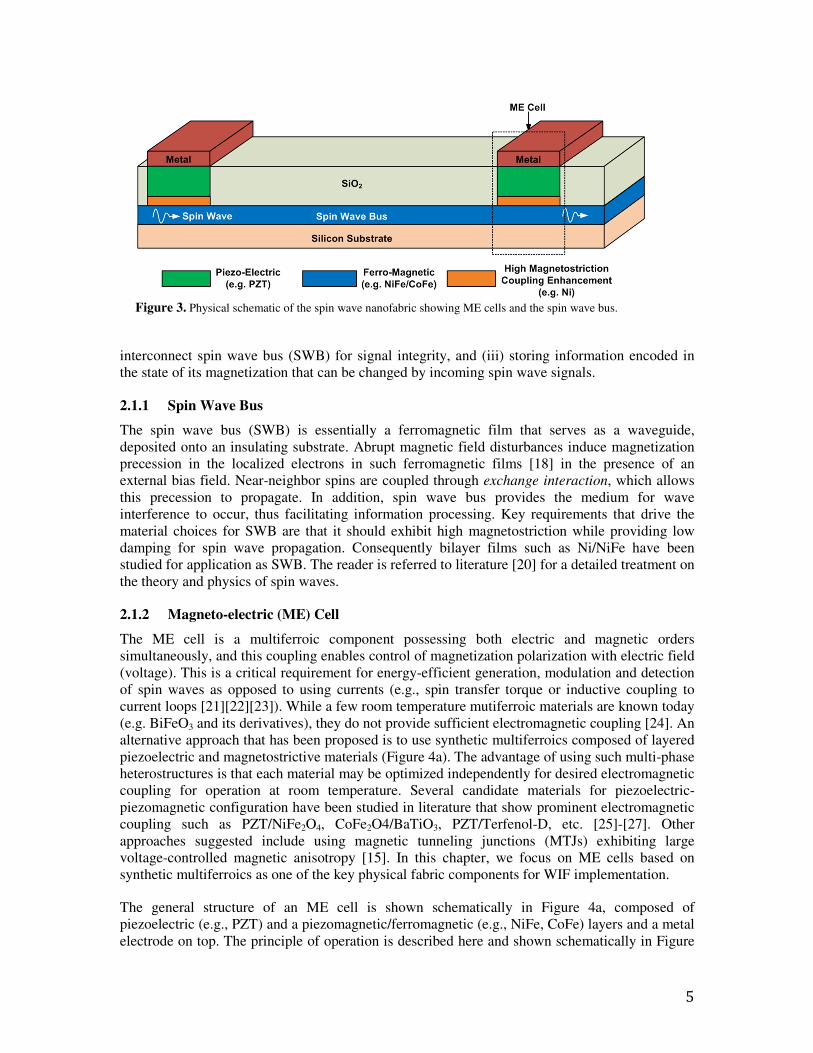
5
interconnect spin wave bus (SWB) for signal integrity, and (iii) storing information encoded in
the state of its magnetization that can be changed by incoming spin wave signals.
2.1.1 Spin Wave Bus
The spin wave bus (SWB) is essentially a ferromagnetic film that serves as a waveguide,
deposited onto an insulating substrate. Abrupt magnetic field disturbances induce magnetization
precession in the localized electrons in such ferromagnetic films [18] in the presence of an
external bias field. Near-neighbor spins are coupled through exchange interaction, which allows
this precession to propagate. In addition, spin wave bus provides the medium for wave
interference to occur, thus facilitating information processing. Key requirements that drive the
material choices for SWB are that it should exhibit high magnetostriction while providing low
damping for spin wave propagation. Consequently bilayer films such as Ni/NiFe have been
studied for application as SWB. The reader is referred to literature [20] for a detailed treatment on
the theory and physics of spin waves.
2.1.2 Magneto-electric (ME) Cell
The ME cell is a multiferroic component possessing both electric and magnetic orders
simultaneously, and this coupling enables control of magnetization polarization with electric field
(voltage). This is a critical requirement for energy-efficient generation, modulation and detection
of spin waves as opposed to using currents (e.g., spin transfer torque or inductive coupling to
current loops [21] [22] [23]). While a few room temperature mutiferroic materials are known today
(e.g. BiFeO3 and its derivatives), they do not provide sufficient electromagnetic coupling [24]. An
alternative approach that has been proposed is to use synthetic multiferroics composed of layered
piezoelectric and magnetostrictive materials (Figure 4a). The advantage of using such multi-phase
heterostructures is that each material may be optimized independently for desired electromagnetic
coupling for operation at room temperature. Several candidate materials for piezoelectric-
piezomagnetic configuration have been studied in literature that show prominent electromagnetic
coupling such as PZT/NiFe2O4, CoFe2O4/BaTiO3, PZT/Terfenol-D, etc. [25]- [27]. Other
approaches suggested include using magnetic tunneling junctions (MTJs) exhibiting large
voltage-controlled magnetic anisotropy [15]. In this chapter, we focus on ME cells based on
synthetic multiferroics as one of the key physical fabric components for WIF implementation.
The general structure of an ME cell is shown schematically in Figure 4a, composed of
piezoelectric (e.g., PZT) and a piezomagnetic/ferromagnetic (e.g., NiFe, CoFe) layers and a metal
electrode on top. The principle of operation is described here and shown schematically in Figure
Figure 3. Physical schematic of the spin wave nanofabric showing ME cells and the spin wave bus.

6
4b-d [28]. A bias voltage applied on the metal electrode generates a stress in the piezoelectric
layer. This causes a rotating of the easy axis in the piezomagnetic material through strain-induced
anisotropy, with two preferred directions (along or opposite to the new easy axis). The angle of
rotation of the easy axis is determined by the strength of the applied electric field. Thus, an
applied voltage results in a change in the magnetic polarization of the ferromagnetic material, and
vice versa. Based on this principle, ME cells can be used to generate and detect spin waves as
follows [29]. An alternating voltage at the top metal contact induces an oscillating strain in the
piezoelectric layer. This creates an alternating strain-induced anisotropy in the magnetostrictive
layer resulting in magnetoelastic spin wave excitation. This generated spin wave propagates
through the spin wave bus to other physical locations. Detection of spin waves occurs through the
reverse process from magnetic to electric domain.
One challenge associated with propagating spin waves is the exponential decay of amplitude with
Figure 4. Schematic showing a) ME cell structure with synthetic multiferroics, and b-d) Principle of operation
for voltage-controlled magnetization rotation in ME Cell (inspired by ref. [11]). (b) When the applied voltage
(Vapp) on metal electrode is 0, the magnetization (�� ) of ferromagnetic material is along the external bias magnetic
field (��������) in the z-direction. (c) When a non-zero voltage is applied (Vapp > 0), the easy axis of the ferromagnetic
film in the ME cell starts to rotate in the y-z plane. This rotation has two possible directions – one with a positive
y-axis component and the other with negative y-axis component. The final direction is determined by the phase of
the incoming spin wave. (d) When the applied voltage reached a critical value (Vmax), the easy axis rotates by a
maximum of 90 degrees. The ME cell then has the highest magnetization component in the y-direction. The
energy diagram (bottom) shows two stable states at the end of the easy axis rotation, which can be used to encode
two logic states. The energy barrier (ΔE) between the two states depends on Vapp, and is highest at Vapp = Vmax.

7
distance due to magnon-phonon, magnon-magnon and other scattering processes. To overcome
this, they need to be amplified to compensate the losses incurred during spin wave propagation.
ME cells provide an efficient way to implement local amplifiers for restoring spin wave
amplitudes in a magnonic circuit via magnetoelectric coupling [30]. Based on the same principle
of voltage-controlled magnetization rotation, when an alternating voltage (required for 90 degree
rotation) is applied at the top metal contact in an ME cell at a frequency equal to the incoming
spin wave frequency, the rotated magnetization component can be amplified to the saturation
value of magnetization. The phase of the incoming spin wave determines the direction of rotation
(along or opposite to rotated direction) and hence preserves the phase in the output wave.
Magnetostatic surface spin waves propagating perpendicular to external magnetic field can travel
up to hundreds of microns at room temperature before requiring amplification [30]. Other
approaches have also been studied in literature such as using electric current for spin wave
pumping [31] and parametric microwave spin wave amplification (using alternating magnetic
fields) [32]- [36]. However, such approaches have disadvantages such as high power consumption
for current-based approach, and undesired direct coupling between microstrips via stray fields in
the microwave amplification approach.
The ME cell is also capable of storing data. When a bias voltage is applied on the top metal
contact, the resultant ME cell magnetic polarization exhibits two stable states (points of minimum
energy in Figure 4c-d bottom panel). This bistability allows the ME cell to store data encoded in
the magnetic polarization of the ferromagnetic layer [11]. Depending on the phase of the
incoming spin wave, the magnetic polarization direction of the ME cell can be switched between
the two states by the exchange field. As long as the voltage is applied the ME cell maintains the
new polarization (state) after switching, thus acting as a latch. The switching between the two
stable states exhibits a threshold behavior. If the exchange field produced by the incoming spin
wave is higher than the coercive field, the energy barrier (ΔE in Figure 4c-d) between the states
can be surmounted. This threshold value is determined by the material choices and strength of
electromagnetic coupling. The switching threshold can also be controlled via the applied voltage
to either make the ME cell susceptible to switching or to make it immune to incoming spin waves
as required.
The main challenge when integrating ME cells with spin wave bus is the preservation of magnetic
bistability of the ME cells. The energy barrier between the two stable states can be significantly
affected by the magnetic field produced in the spin wave bus. The geometry and dimensions of
the ME cell and spin wave bus have to be engineered to ensure that sufficient coupling is
achieved without compromising ME cell bistability. Micromagnetic simulation studies have
shown that thermally robust bistability of the cell magnetization can be achieved with a suitable
choice of parameters, and can be improved by increasing the cell thickness and saturation
magnetization while reducing the bus thickness and saturation magnetization [15].
To summarize, in this section we presented an overview on the spin wave physical layer used for
WIF framework. Spin waves were defined and the physical components required to operate on
spin waves were discussed briefly. In the next section, we discuss the WIF elementary operators
that are natively supported by these physical components to realize logic operations.
3 Elementary WIF Operators for Logic
Here, we introduce the notations and elementary WIF operators that will be used in the following
sections for WIF logic design. A spin wave is represented as ��; the ‘~’ accent indicates this is a
wave. Using this notation, a wave is represented using polar co-ordinates to incorporate both its
amplitude (a) and phase (φ) compactly as follows:

8
�� �� ���� � � � ��� ��. (1)
We limit the phase to be either 0 or π in the data encoding used in this chapter, since the ME cells
used for spin wave detection are designed to differentiate these phases. Using this notation, any
wave can be interpreted as having amplitude a when the phase is 0, and –a when the phase is π at
the point of interference. Additional phases may be used as per physical component capabilities
as well. When a phase other than 0 and π is employed, either the real or imaginary component of
the notation above will need to be used as required.
To represent data in radix-r number system, we need r/2 distinct amplitude values if r is even,
and (r+1)/2 amplitude values if r is odd, in conjunction with aforementioned 2 phase values. For
example, for binary data representation (radix-2) we need a single amplitude level A. The phase
encodes binary data (1-bit) with logic 0 and logic 1, assigned to waves with initial phase 0 and π
respectively. For quaternary data representation (radix-4), we use two amplitude levels (A, 3A) in
conjunction with two phase values (0, π) to get four different combinations. Each combination is
assigned to a logic value (see Figure 2b). Alternative combinations for amplitude and phase may
also be used.
Interference Operator: Wave interference is the fundamental operation in the WIF approach. As
mentioned earlier, spin waves interfering at a given point exhibit linear superposition behavior.
Thus an Interference Function I of n input waves is defined as follows:
�����, ���, … , ����� ��� � ��� �⋯� �����
��� # � ��� $ �⋯� ����� %&$ . (2)
The result of this Interference Function I is again a spin wave '� , whose individual wave
attributes are denoted as follows:
'� (�� ) �����, ���, … , �����
where, ( I+����, ���, … , �����
�( I ����, ���, … , ����� .
(3)
Here, note that IA(.) and I
φ(.) are not in bold since they represent individual wave attributes. The
circuit schematic for the Interference Function used in this chapter is shown in Figure 5.
Consider a wave interference of 3 inputs ���, ���, ��, with equal amplitudes A but differing in
phase. All possible input combinations and the result of interference operation are shown in Table
1. Looking at the output interpretation column, we see that the output phase of the interference
operation is a majority of input wave phases, i.e.
when 2 or more input waves have same phase the
output wave assumes that phase. This property can be
used to implement majority logic [12] using
Interference Function. Notice that the amplitude of
the output wave has additional information as well –
it represents the number of input waves that have the
same phase. Thus the Interference Function is much
more than a simple majority, and it results in a spin
Figure 5. Schematic representation for
interference function.

9
wave that encodes all the necessary information about the inputs in a compressed manner.
In general for n input waves, if the amplitude of any wave ��- is aj = wj.A, where wj represents a
weight in multiples of unit-amplitude A, then the Interference Function result encodes the
following information:
I ����, ���, … , ����� = ./; �1 ∑ 3-4��5 > ∑ 374���
0; �9�� → weighted- majority decision
I+����, ���, … , ����� = ;∑ 374���; − ;∑ 3-4��5; . (4)
To understand the circuit-level implication of this additional information at the output of the
Interference Function for logic vs. conventional majority function, we take an example of
constructing a 5-input majority to be implemented with a network of 3-input majority functions.
To implement this with Interference Functions, the network can be built as follows by grouping
primary inputs into groups of 3, and applying the definition of Interference Function:
�����, ���, ��,, ��=, ��> = ��� + ��� + ��, + ��= + ��> = �?����, ���, ��, + ��= + ��>
= '� + ��= + ��> , 3ℎ�A� '� = �?����, ���, ��,
= �B�'�, ��=, ��> . Thus we get,
�����, ���, ��,, ��=, ��> = �B��?����, ���, ��, , ��=, ��> , (5)
and the majority decision is given by the phase of the final Interference Function I,
. The network
of Interference Functions represented by the equation above is shown in Figure 6a.
For conventional majority function, this approach does not work. In fact, the minimal network to
implement this is obtained using the following expression [37] and shown in Figure 6b:
CD�E�, E�, E,, E=, E>� = CD�E�, CD�E,, E=, E>�, CD�E�, E,, CD�E�, E=, E>���. (6)
Clearly the network of conventional majority functions is more complex (requires 4 majority
functions) than the Interference Function network (needs only 2 Interference Functions). The
intuition for this result is that the output of a conventional majority records only the majority
decision and does not encode additional information about the primary inputs, thus some
information is lost. This necessitates the regeneration of information using other gates as shown.
TABLE 1. INTERFERENCE OPERATION ON THREE INPUT WAVES
Input Waves
{���, ���, ��,} �����, ���, ��,
Output Interpretation
Wave
Amplitude
Wave Phase
(Weighted Majority
Decision)
No. of inputs with same
phase (Additional
Information)
{4���, 4���, 4���} 34��� 3A 0 3
{4���, 4���, 4��G} 4��� A 0 2
{4���, 4��G, 4��G} 4��G A π 2
{4��G, 4��G, 4��G} 34��G 3A π 3

10
On the other hand, the Interference Function output encodes all the information about primary
inputs in wave amplitude and phase – i.e. the phase encodes weighted majority decision while
amplitude encodes the number of inputs that led to the majority. Thus the Interference Function
network obviates the need to replicate primary inputs, leading to a much smaller network. This
example shows that a network of Interference Functions can potentially lead to compact
implementation for a given logic function than conventional majority.
The Interference Function can be used to realize Boolean logic as well, but this approach would
be inefficient and would not harness its full potential. We mention this approach for a
comprehensive treatment on the possible applications of Wave Interference Functions. Consider
the same 3-input Interference Function mentioned earlier. By using one of the inputs as a control
signal (HI� with constant amplitude and phase we can realize Boolean AND and OR operations
between the other two inputs, as shown in Table 2. In fact, WIF logic can be made reconfigurable
to act as Boolean AND or OR logic by dynamically changing the control signal.
Identity Operator: The identity operator takes an input wave and provides the same wave at the
output. This is analogous to a wire in the electrical domain, which maintains the same voltage at
Figure 6. Comparison of implementation of 5-input majority using: a) Wave Interference Functions; and b)
Conventional majority functions.
TABLE 2. BOOLEAN LOGIC WITH WIF INTERFERENCE OPERATOR
Operation
JK
Control
Input Waves
��JK, LKM, LK?
Output
Wave
Amplitude
Wave
Phase
Boolean
Interpretation LKM LK?
AND
4��� 4��� 4��� 34��� 34 3A 0 Logic 0
4��� 4��� 4��G 4��� 4 A 0 Logic 0
4��� 4��G 4��� 4��� 4 A 0 Logic 0
4��� 4��G 4��G 4��G <4 A π Logic 1
OR
4��G 4��� 4��� 4��� = 4 A 0 Logic 0
4��G 4��� 4��G 4��G = −4 A π Logic 1
4��G 4��G 4��� 4��G = −4 A π Logic 1
4��G 4��G 4��G 34��G <34 3A π Logic 1

11
the output as the input. In WIF, the identity operator is simply a spin wave bus whose length is an
integral multiple of the wavelength. This ensures that the output phase is the same as the input
wave phase.
Complement Operator: This performs the inversion function. Logic realization using WIF requires a complement operator to be functionally complete. For radix-r, this function is represented using the following equation:
E = �A − 1� − E, where E ϵ {0, 1,…, r-1}. (7)
Here, x represents the logical input value in radix-r number system. This is analogous to a
Boolean NOT operation. Given a spin wave �� = �� , the complement operator (with “–“ sign)
is defined as follows:
<�� <��� � ��� P5� .<; ifφ 0; ifφ π
(8)
Physically, this means that the inversion operator introduces a phase shift of π for a given spin
wave, as a consequence of the choice of data representation.
Physical implementation of elementary WIF operators: The physical implementation of the WIF
operators turns out to be quite simple without requiring any active devices (see Figure 7). The
Interference Function is simply a junction of spin wave buses. The identity operator is a spin
wave bus whose length is an integral multiple of the wavelength (λ). This ensures that the output
phase is the same as the input wave phase. The complement operator can be implemented by
using a spin wave bus that has a length equal to an odd multiple of the half-wavelength.
4 Binary WIF Logic Design
Binary WIF is one instance of the generic multi-valued WIF paradigm. Here, data is encoded
using two discrete values of wave phase only. The amplitudes of input waves are all the same
value A, as shown in Table 3. In this section, we illustrate binary WIF logic design with
elementary WIF operators using example circuits such as full adders and parallel counters. These
circuits are evaluated and compared to equivalent CMOS Boolean circuits for estimating the
Figure 7. Physical implementation of WIF binary operators with spin wave bus (SWB). a) The
interference function is implemented by simply joining SWBs; b) The identity operator is a SWB whose
length is an integral multiple of the spin wavelength; and c) The inversion operator is a SWB with
length equal to an odd multiple of half wavelength of spin wave to realize a π-shift in phase at the
output. Here n is an integer in (b) and (c).

12
benefits of WIF in terms of power, performance and area. We also present a range of possible
WIF layout topologies for adder circuits and discuss the impact of each design on physical
requirements.
4.1 Binary WIF Full Adder
This circuit is widely used in various arithmetic operations today and hence its WIF design is
treated here. A binary full adder is a 3-input, 2-output logic circuit that performs addition of the
inputs (A, B, CIN). The output is encoded in the binary domain using weighted bits (COUT – most
significant bit with weight 21, and Sum – least significant bit with weight 2
0). One way to
implement adder functionality with WIF is to use the Boolean logic implementation, and simply
replace the Boolean logic gates with equivalent Interference Functions (Boolean function
implementation with Interference Functions was discussed earlier). However this approach would
be inefficient, as it would not harness the full potential of Interference Functions.
Since wave interference fundamentally performs addition of amplitudes for in-phase waves and
subtraction for out-of-phase waves, a single Interference Function would implemenent a full
adder in principle. If 4I, U� , HIVW are input waves corresponding to binary logical inputs A, B, CIN
respectively, then the output wave of the interference operation is:
TABLE 3. BINARY DATA ENCODING
Logic Value Wave Representation Wave Attributes
0 X�� = 4��� (Phase 0, Amplitude A)
1 X�� = 4��5 (Phase π, Amplitude A)
TABLE 4. TRUTH TABLE OF 1-BIT FULL ADDER SHOWING ALL POSSIBLE OUTPUT COMBINATIONS.
Logic Representation Corresponding Output Wave (YK?) Attributes
A B CIN COUT Sum Phase Amplitude
0 0 0 0 0 0 3A
0 0 1 0 1 0 A
0 1 0 0 1 0 A
0 1 1 1 0 π A
1 0 0 0 1 0 A
1 0 1 1 0 π A
1 1 0 1 0 π A
1 1 1 1 1 0 3A
TABLE 5: LIST OF UNIQUE OUTPUT COMBINATIONS
COUT Sum Wave Phase
I�Z�[K, \K, JK]^
Wave Amplitude
I�_�[K, \K, JK]^
0 0 0 3A
0 1 0 A
1 0 π A
1 1 π 3A

13
'�� = �?�4I, U� , HIVW . (9)
Consider the truth table of a 1-bit full adder shown in Table 4, with all possible input/output
combinations along with amplitude and phase of the WIF output wave YK?. A list of possible
unique outcomes of addition along with corresponding wave attributes is shown in Table 5. It can
be observed that a combination of output wave phase and amplitude encodes all information
pertaining to the result of addition in the multi-valued domain.
Given our objective to implement a binary full adder, we need to decode this multi-valued output
wave into corresponding binary outputs. From Table 4 and Table 5, it can be observed that COUT
is logic 1 (phase π) when at least 2 inputs are logic 1. Thereby, COUT is essentially the majority
outcome of the three interfering waves which is encoded in the phase [IZ�4K, U, H� ab�] of the output
wave. In order to generate the Sum bit, we need to translate information in the combination of
output wave amplitude and phase, into the phase of a new wave.
In binary number system, the addition of logical inputs A, B, CIN can be expressed as:
4 + U + HVW = 2�. Hefg + 2�. hiC. hiC = �4 + U + HVW� − 2Hefg .
(10)
Converting this logical equation into corresponding Interference Function expression:
hiCj = �4I + U� + HIVW − 2k4. ��� ��l ; 3ℎ�A� �1 Hefg = I �4I, U� , HIVW
= �?�4I, U� , HIVW − 'K2 ; 3ℎ�A� 'K2 = 24����1�
= �Bk'K1, −'K2l ; 3ℎ�A� 'K1 �?�4K , UK , HKab
(11)
Thus the effect of MSB (COUT) needs to be eliminated from the output wave of the first
interference, in order to extract the LSB (Sum). This is accomplished by an Interference Function
between the output of the first interference and a control wave of amplitude 2A, which is out-of-
phase with respect to the original compressed output wave from the first Interference Function. A
complete list of possible outcomes of 1-bit adder along with the required baising inputs are shown
in Table 6. Thus the outputs of the binary full adder are expressed in terms of Interference
Functions as follows:
Hefg = I �4I, U� , HIVW (12)
TABLE 6: LIST OF UNIQUE OUTPUTS OF 1-BIT ADDER ALONG WITH REQUIRED CONTROL WAVE TO
GENERATE THE SUM OUTPUT
COUT Sum YK?= ��[K, \K, JK]^
(Amp, phase)
Control Wave YKB
(Amp, phase)
Final Sum output
(Amp, phase)
0 0 (3A,0) (2A, π) (A, 0)
0 1 (A,0) (2A, π) (A, π)
1 0 (A, π) (2A, 0) (A, 0)
1 1 (3A, π) (2A, 0) (A, π)

14
hiC = I ��?�4I, U� , HIVW ,<'�, ; 3@�A�'�, 24���mnop�. (13)
Figure 8A shows the schematic representation of the above logic equations, and the
corresponding WIF layout is shown in Figure 8B. The schematic shows two types of waves— (i)
waves with information in phase only (shown in blue); and (ii) waves with information both in
phase and amplitude (shown in red). As per logic equations, the three primary waves interfere to
generate '��. This first interference I1 acts as a ‘pre-computation’ step which is later used for
extracting both COUT and Sum bits. It is interesting to note that while inputs and outputs are binary,
new physical phenomenon like spin waves encode additional information pertaining to primary
inputs in the internal multi-valued signals in a compressed manner, leading to simple circuit
implementation. The Boolean and majority based implementation of the full adder using WIF
would have resulted in more complex network of Interference Functions, and is left to the reader
as an exercise.
4.2 Parallel Counters
We now show another important type of combinational circuit called as (n, m) Parallel Counter.
These are digital circuits with n inputs and m = log2(n+1) output bits; the output represents the
Figure 8. a) Schematic diagram showing implementation of 1-bit full adder using WIF. b) Layout of 1-bit WIF
full adder using ME cells and waveguides. Note that unless specified otherwise, all waveguides shown in the
layout are of length ‘nλ’.

15
number of 1’s in the n-input bit set [38]. Generally, parallel counters are used in the
implementation of fast parallel multipliers. However, counters are more complex than full adders
and quickly result in complex netlists as the multiplier bit-width is increased. This is because
CMOS gates have limited fan-in, and hence practical designs limit the parallel counter size to (7,
3) or use an even smaller version known as a (4, 2) compressor [38]. By contrast, WIF allow for
highly simplified implementations of high bit-width parallel counters due to compressed multi-
valued data representation at the output of an Interference Function. Figure 9 shows WIF based
(7, 3) parallel counter implementation derived by extending the approach outined for full adder,
and is expressed using the following Interference Functions. If 4I�, 4I�, … , 4Iq represent input
waves corresponding to primary logical inputs A0, A1,…, A6, let
'�� �?�4I�, 4I�, … , 4Iq ;
'�= �B�'��, <'�, ; where '�, 44��st and u, I�Z�4I�, 4I�, … , 4Iq� '�v �w�'��, <'�,, <'�> ; where '�> 24��sx and u> I,Z�'��, <'�,�. (14)
The output bits are extracted from the phase of the resultant waves as follows:
y, I�Z�4I�, 4I�, … , 4Iq� – MSB
y� I,Z�'��, <'�,� y� I=Z�'��, <'�,, <'�>�. – LSB (15)
From Figure 9 it is evident that a large portion of the layout is consumed by the patterning needed
for creating the interference of all the primary inputs. Without the compressed data representation
at the output of an Interference Function, the layout would have required replication of primary
inputs for all output bits. This would lead to a much larger physical implementation and
consequently larger area and delay of the overall circuit. It is expected that high bit-width designs
would have even higher benefits due to the compressed data representation feature.
Using a similar approach we also show the logic equations for a (15, 4) parallel counter and the
Figure 9. WIF layout of (7,3) parallel counter [15]. All the inputs are first compressed into a single wave which is
later used to generate the output bits. Note that unless specified otherwise, all waveguides shown in the layout are
of length ‘nλ’.
16
layout is shown in Figure 10.
Step1: Defining individual Interference Functions
'�� = ��4I�, 4I�, … , 4I�>
'�= ��'��, <'�, where '�, 84��st and u, IZ�4I�, 4I�, … , 4I�>� '�v ��'��, <'�,, <'�> where '�> 44��sx and u> IZ�'��, <'�,� '�{ ��'��, <'�,, <'�>, <'�q where '�q 24��s| and uq IZ�'��, <'�,, <'�>� (16) Step2: Output Functions
y= IZ�4I�, 4I�, … , 4I�>� y, IZ�'��, <'�,� y� IZ�'��, <'�,, <'�>� y� IZ�'��, <'�,, <'�>, <'�q�. (17)
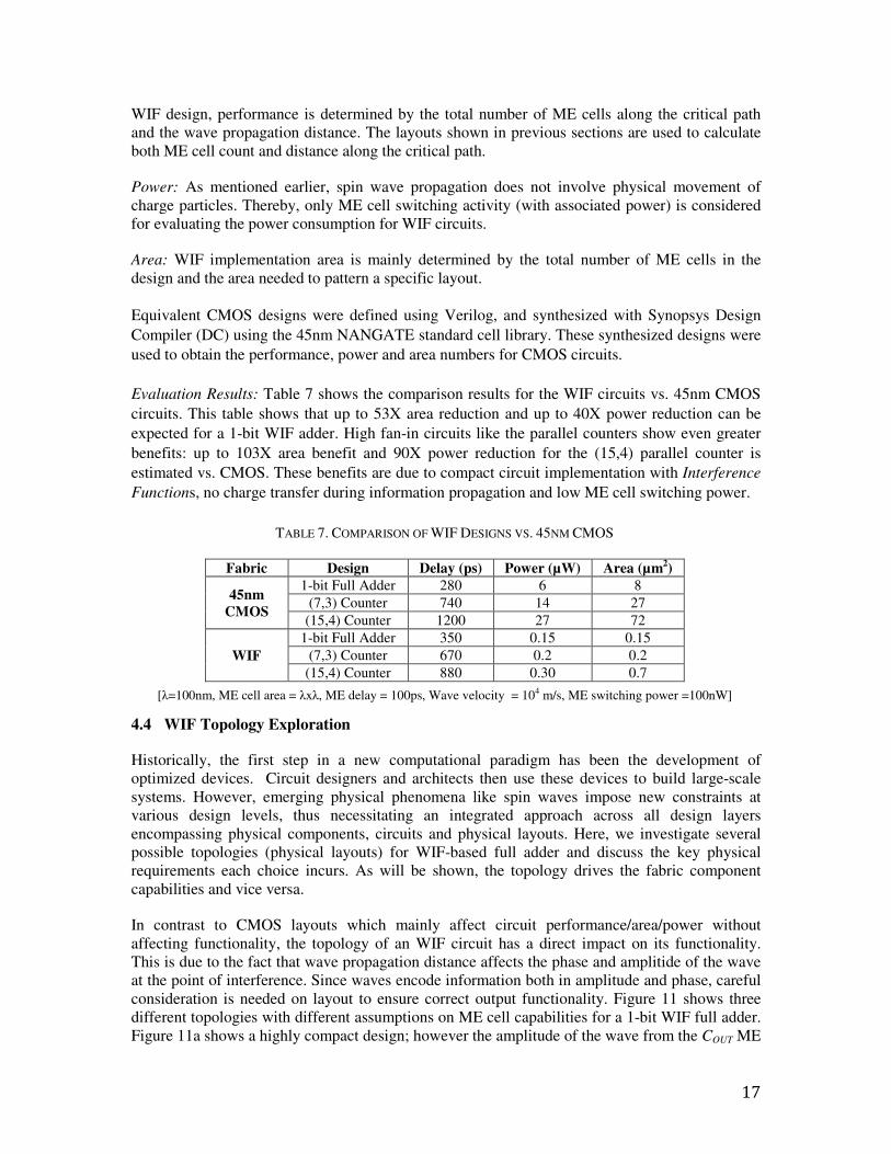
4.3 Benchmarking Binary WIF Circuits vs. CMOS
Here, we evaluate the adder and parallel counter designs presented previously in terms of power,
delay and area metrics. We compare them to equivalent 45nm CMOS designs to estimate the
benefits of WIF approach. WIF fabric parameters used for evaluation are based on theoretical
simulations and experimental evidence [21] [22] and are as follows. For all evaluations shown in
this chapter, ME cell dimension of 100nm x 100nm with a switching delay of 100ps is used.
Based on a simple capacitive approximation, ME cell switching energy is calculated to be around
10aJ per switching. For delay calculations in the waveguides, spin wave group velocity is
assumed to be 104m/s. Assuming that spin waveguides have the same patterning limitations as
45nm CMOS designs, the width of waveguides and spacing between ME cells is assumed to be
45nm for area estimations shown in this section. The methodology followed for WIF design
evaluations is discussed next.
Performance: In digital circuits, performance is determined by the delay along the critical path in
the design. Critical path is the path between inputs and outputs with maximum delay. For
example, the path from the inputs to the Sum output bit is the critical path in a 1-bit adder. For the
Figure 10. WIF layout of (15,4) parallel counter. High fan-in circuits benefit more from the data compression
feature. Note that unless specified otherwise, all waveguides shown in the layout are of length ‘nλ’.
17
WIF design, performance is determined by the total number of ME cells along the critical path
and the wave propagation distance. The layouts shown in previous sections are used to calculate
both ME cell count and distance along the critical path.
Power: As mentioned earlier, spin wave propagation does not involve physical movement of
charge particles. Thereby, only ME cell switching activity (with associated power) is considered
for evaluating the power consumption for WIF circuits.
Area: WIF implementation area is mainly determined by the total number of ME cells in the
design and the area needed to pattern a specific layout.
Equivalent CMOS designs were defined using Verilog, and synthesized with Synopsys Design
Compiler (DC) using the 45nm NANGATE standard cell library. These synthesized designs were
used to obtain the performance, power and area numbers for CMOS circuits.
Evaluation Results: Table 7 shows the comparison results for the WIF circuits vs. 45nm CMOS
circuits. This table shows that up to 53X area reduction and up to 40X power reduction can be
expected for a 1-bit WIF adder. High fan-in circuits like the parallel counters show even greater
benefits: up to 103X area benefit and 90X power reduction for the (15,4) parallel counter is
estimated vs. CMOS. These benefits are due to compact circuit implementation with Interference
Functions, no charge transfer during information propagation and low ME cell switching power.
4.4 WIF Topology Exploration
Historically, the first step in a new computational paradigm has been the development of
optimized devices. Circuit designers and architects then use these devices to build large-scale
systems. However, emerging physical phenomena like spin waves impose new constraints at
various design levels, thus necessitating an integrated approach across all design layers
encompassing physical components, circuits and physical layouts. Here, we investigate several
possible topologies (physical layouts) for WIF-based full adder and discuss the key physical
requirements each choice incurs. As will be shown, the topology drives the fabric component
capabilities and vice versa.
In contrast to CMOS layouts which mainly affect circuit performance/area/power without
affecting functionality, the topology of an WIF circuit has a direct impact on its functionality.
This is due to the fact that wave propagation distance affects the phase and amplitide of the wave
at the point of interference. Since waves encode information both in amplitude and phase, careful
consideration is needed on layout to ensure correct output functionality. Figure 11 shows three
different topologies with different assumptions on ME cell capabilities for a 1-bit WIF full adder.
Figure 11a shows a highly compact design; however the amplitude of the wave from the COUT ME
TABLE 7. COMPARISON OF WIF DESIGNS VS. 45NM CMOS
Fabric Design Delay (ps) Power (µW) Area (µm2)
45nm
CMOS
1-bit Full Adder 280 6 8
(7,3) Counter 740 14 27
(15,4) Counter 1200 27 72
WIF
1-bit Full Adder 350 0.15 0.15
(7,3) Counter 670 0.2 0.2
(15,4) Counter 880 0.30 0.7
[λ=100nm, ME cell area = λxλ, ME delay = 100ps, Wave velocity = 104 m/s, ME switching power =100nW]
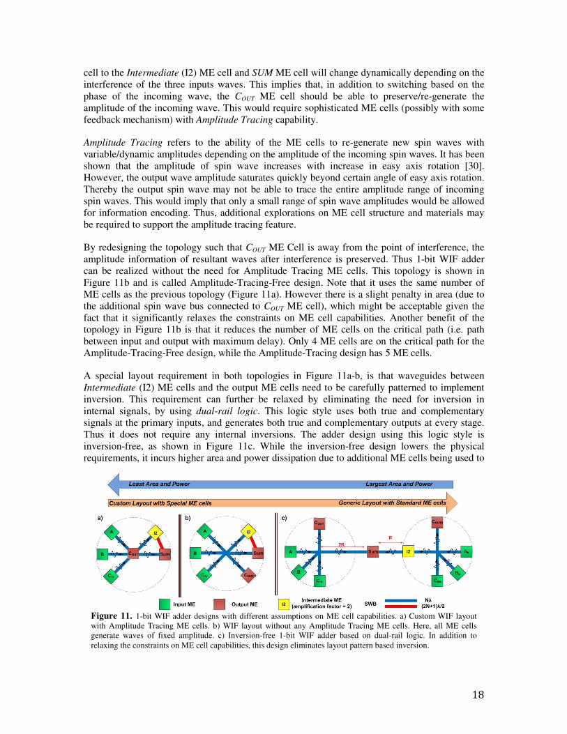
18
cell to the Intermediate (I2) ME cell and SUM ME cell will change dynamically depending on the
interference of the three inputs waves. This implies that, in addition to switching based on the
phase of the incoming wave, the COUT ME cell should be able to preserve/re-generate the
amplitude of the incoming wave. This would require sophisticated ME cells (possibly with some
feedback mechanism) with Amplitude Tracing capability.
Amplitude Tracing refers to the ability of the ME cells to re-generate new spin waves with
variable/dynamic amplitudes depending on the amplitude of the incoming spin waves. It has been
shown that the amplitude of spin wave increases with increase in easy axis rotation [30].
However, the output wave amplitude saturates quickly beyond certain angle of easy axis rotation.
Thereby the output spin wave may not be able to trace the entire amplitude range of incoming
spin waves. This would imply that only a small range of spin wave amplitudes would be allowed
for information encoding. Thus, additional explorations on ME cell structure and materials may
be required to support the amplitude tracing feature.
By redesigning the topology such that COUT ME Cell is away from the point of interference, the
amplitude information of resultant waves after interference is preserved. Thus 1-bit WIF adder
can be realized without the need for Amplitude Tracing ME cells. This topology is shown in
Figure 11b and is called Amplitude-Tracing-Free design. Note that it uses the same number of
ME cells as the previous topology (Figure 11a). However there is a slight penalty in area (due to
the additional spin wave bus connected to COUT ME cell), which might be acceptable given the
fact that it significantly relaxes the constraints on ME cell capabilities. Another benefit of the
topology in Figure 11b is that it reduces the number of ME cells on the critical path (i.e. path
between input and output with maximum delay). Only 4 ME cells are on the critical path for the
Amplitude-Tracing-Free design, while the Amplitude-Tracing design has 5 ME cells.
A special layout requirement in both topologies in Figure 11a-b, is that waveguides between
Intermediate (I2) ME cells and the output ME cells need to be carefully patterned to implement
inversion. This requirement can further be relaxed by eliminating the need for inversion in
internal signals, by using dual-rail logic. This logic style uses both true and complementary
signals at the primary inputs, and generates both true and complementary outputs at every stage.
Thus it does not require any internal inversions. The adder design using this logic style is
inversion-free, as shown in Figure 11c. While the inversion-free design lowers the physical
requirements, it incurs higher area and power dissipation due to additional ME cells being used to
Figure 11. 1-bit WIF adder designs with different assumptions on ME cell capabilities. a) Custom WIF layout
with Amplitude Tracing ME cells. b) WIF layout without any Amplitude Tracing ME cells. Here, all ME cells
generate waves of fixed amplitude. c) Inversion-free 1-bit WIF adder based on dual-rail logic. In addition to
relaxing the constraints on ME cell capabilities, this design eliminates layout pattern based inversion.

19
generate dual-rail signals. This exploration shows that WIF offers a wide range of physical
topologies, which can be tuned to meet a given design objective as required.
In summary, we have illustrated WIF binary logic design using adders and parallel counters as
examples. Benchmarking for these circuits was presented against equivalent 45nm CMOS circuits
in terms of power, area and performance. We have also discussed the effect of WIF physical
topology on fabric component requirements. Binary WIF logic is a special instance of multi-
valued WIF, where the information in the input waves is encoded only in wave phase using two
discrete values. The next section presents the generic WIF multi-valued logic framework.
5 Multi-valued WIF Logic Design
Multi-valued logic is defined as the logical calculus that involves more than two logic levels. It
allows compact data and functional representations, and is more efficient compared to binary
logic. As a result, multi-valued logic implementations have been long sought for both general
purpose processors and for applications that are inherently more suitable for multi-valued
computations such as: image processing, big data analytics, many-valued decision diagrams,
artificial neural networks etc. However, the transition from binary to multi-valued logic based
implementations has been unsuccessful so far, since conventional approaches use digital CMOS
technology, which is tailored for binary logic and operates with binary switches, for hardware
emulation of multi-valued constructs that is very inefficient.
In contrast to CMOS, WIF's inherent features allow data representation and computation in
multi-valued domain natively. Multiple logic levels can be encoded in a combination of wave
amplitude and phase, and multi-valued computation performed through interference and
superposition of propagating spin waves. ME cells are used for generation and amplification of
spin waves of different amplitudes and phases, and spin wave buses are used to facilitate wave
interactions. Since intrinsic properties of core fabric components are utilized for multi-valued
computation, the implementation results in orders of magnitude efficiencies compared to
traditional CMOS based approaches. In this section, we present multi-valued logic
implementation using WIF. Multi-valued data representation in-terms of spin wave’s amplitude
and phase is discussed first, and is followed by definition and implementation of multi-valued
operators, and example circuits. Finally, benchmarking results and implementation of
input/output logic for interfacing with binary logic are presented.
Data representation and multi-valued information encoding using multiple spin wave attributes
was introduced in Section 2.1. Examples of multi-valued representations with two different
phases (phase 0 and phase π) and amplitudes (amplitude A and amplitude 3A) for quaternary
(radix-4) logic are shown in Table 8. This representation is used in following sections to illustrate
quaternary WIF fabric as an example of multi-valued WIF circuits.
TABLE 8. QUATERNARY (RADIX-4) LOGIC ENCODING
Logic Value Wave Representation Wave Attributes
0 X�� = 34��� (Phase 0, Amplitude 3A)
1 X�� = 4��� (Phase 0, Amplitude A)
2 X�, = 4��5 (Phase π, Amplitude A)
3 X�= = 34��5 (Phase π, Amplitude 3A)
20
5.1 Multi-valued Operators and Implementation using WIF
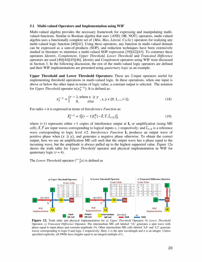
Multi-valued algebra provides the necessary framework for expressing and manipulating multi-valued functions. Similar to Boolean algebra that uses {AND, OR, NOT} operators, multi-valued algebra uses a functionally complete set of {Min, Max, Literal, Cyclic} operators for realizing any multi-valued logic function [40] [41]. Using these operators, any function in multi-valued domain can be expressed as a sum-of-products (SOP), and reduction techniques have been extensively studied in literature to minimize a multi-valued SOP expression [39] [42] [43]. To construct these operators Identity, Complement, Upper Threshold, Lower Threshold and Truncated Difference operators are used [40] [44] [45] [46]. Identity and Complement operators using WIF were discussed in Section 3. In the following discussion, the rest of the multi-valued logic operators are defined and their WIF implementations are presented using quaternary logic as an example.
Upper Threshold and Lower Threshold Operators: These are 2-input operators useful for
implementing threshold operations in mutli-valued logic. In these operations, when one input is
above or below the other input in terms of logic value, a constant output is selected. The notation
for Upper Threshold operator is�E(}���. It is defined as:
E(}�� = .A − 1, whenE � �0,�9�� , E, � ϵ {0, 1,…, r-1}. (18)
For radix–r it is expressed in terms of Interference Function as:
������ = Ik�A < 1�I�Z�<��, '�, X�}/,�l, (19)
where (r-1) represents either r-1 copies of interference output at I1 or amplification (using ME
cell); ��, 'K are input waves corresponding to logical inputs x, y respectively; and X�}/, is a reference
wave corresponding to logic level r/2. Interference Function I1 produces an output wave of positive phase when �E � ��, and generates a negative phase otherwise. To obtain the correct output, here we use an amplification ME cell such that the output wave has a phase equal to the incoming wave, but the amplitude is always pulled up to the highest supported value. Figure 12a shows the truth table for Upper Threshold operator and physical implementation in WIF for quaternary logic (r = 4).
The Lower Threshold operator ( E(}�� ) is defined as
Figure 12. Truth table and physical implementation for a) Upper Threshold Operator; b) Lower Threshold
Operator; c) Truncated Difference Operator. The intermediate ME cell labeled ‘3A’ generates a spin wave with
phase equal to input phase and constant amplitude 3A. Other intermediate ME cells labeled ‘L0’ and ‘L2’ generate
waves corresponding to logic 0 and logic 2 respectively. Here, λ is the spin wavelength and n is an integer. Unless
specified explicitly, all SWBs have lengths equal to an integral multiple of λ.

21
E(}�� = .A − 1, ifE � �0,�9�� . (20)
It is implemented the same way as the Upper Threshold operator, but inputs are interchanged (Figure 12b). The Interference Function to express Lower Threshold operation is:
��(}�� �k�A < 1�I�Z���,<'�, X�}/,�l. (21)
Truncated Difference Operator: This is used to select the difference between two inputs when a
condition is satisfied. The notation is x Ξ y, and the operation is defined as
EΞ� .E < �, whenE 6 �0,�9�� , E, �ϵ�0,1, … , A < 1�. (22)
This can be expressed with Interference Function as
��Ξ'� ����, <'�, X�� , (23)
where, ��, '� are input waves corresponding to logical inputs x, y respectively; and X�� is a reference wave corresponding to logic 0. The truth table and the physical implementation for Truncated Difference operator are shown in Figure 12c for quaternary logic. The difference operation is performed at the junction of incoming waves. In order to achieve the correct output, the resultant wave amplitude after interference is always truncated to 3A if it is greater than 3A. This truncation may be achieved by either designing the spin wave bus and ME cells to accommodate this requirement or through external electrical circuits. The same assumption is considered for other multi-valued operators and circuit implementations as well.
Using these operators, we discuss WIF implementation of Min, Max, Literal and Cyclic operators to enable any arbitrary multi-valued logic function realization.
Min Operator: The min operator in multi-valued logic is similar to the AND operator in Boolean
logic. The operator notation used is (x.y), and is defined as
E ∙ � .E,E � �E < �E < ��,�9�� , E, �ϵ�0,1, … , A < 1�. (24)
The Truncated Difference operator can be used to realize the above output conditions as x ∙ y = x Ξ (x Ξ y). Notice that in equation (13), for the condition x ∙ y = y, the output is re-expressed as x ∙ y =
Figure 13. Truth table and physical implementation for a) Max Operator; b) Min Operator. The intermediate ME
cells labeled ‘L0’ and ‘L3’ generate waves corresponding to logic 0 and logic 3 respectively. Here, λ is the spin
wavelength and n is an integer. Unless specified explicitly, all SWBs have lengths equal to an integral multiple of λ.

22
x – (x – y) to enable implementation with Truncated Difference operator. The functional representation in terms of Interference Function is:
Min���, '� ��Ξ���Ξ'� �k��,<���Ξ'� , X��l, (25)
where ��, '� are input waves corresponding to logical inputs x, y respectively; and X�� is a reference wave corresponding to logic 0. Figure 13a shows the truth table and the WIF physical implementation of Min operator.
Max Operator: The max operator (x + y) in multi-valued logic is analogous to the Boolean OR, defined as follows:
E � � .E,E 6 �E � �� < E�, �9�� , E, �ϵ�0,1, … , A < 1�. (26)
The functional representation in terms of Interference Function is
Max���, '�� �� � �'��� �k��, �'��� , X�}��l, (27)
where X�}�� is a reference wave corresponding to logic value r-1. The WIF implementation and truth table for max operator for quaternary logic is shown in Figure 13b.
Literal Operator: This operator combines both Upper Threshold and Lower Threshold operators, and provides more flexibility for conditional operations. The notation for Literal operator is
px
q.
The output conditions are defined as:
�E� .A < 1, � � E � �0,�9�� , �, �, E, �ϵ�0,1, … , A < 1�. (28)
The Interference Function implementing literal operator using Upper Threshold and Lower Threshold operators is
���� ��������, ������ , X�� . (29)
where LK is the input wave corresponding to logical input x, and ��M is a reference wave
corresponding to logic level 0. This implementation for quaternary logic is shown in Figure 14.
Cyclic Operator: The cyclic operator is also known as mod-sum operator [46]; it performs XOR-like operation in the multi-valued domain. The mod-sum operator is defined as:
Figure 14. Truth table and physical implementation for Literal Operator. The intermediate ME cell labeled ‘3A’
generates a spin wave with phase equal to input phase and constant amplitude 3A. Other intermediate ME cells
labeled ‘L0’ and ‘L2’ generate waves corresponding to logic 0 and logic 2 respectively. Here, λ is the spin
wavelength and n is an integer. Unless specified explicitly, all SWBs have lengths equal to an integral multiple of λ.
23
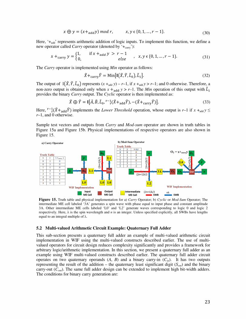
E ⊕ � = �E+�����C��A,E, �ϵ�0,1, … , A < 1�. (30)
Here, ‘+add’ represents arithmetic addition of logic inputs. To implement this function, we define a new operator called Carry operator (denoted by ‘+carry’):
E������� .1, ifE����� 6 A < 10,�9�� , E, �ϵ�0,1, … , A < 1�. (31)
The Carry operator is implemented using Min operator as follows:
��������'� Mink����, '�, X�� , X��l. (32)
The output of I���, '�, X�� represents (x +add y) – r–1, if x +add y > r–1; and 0 otherwise. Therefore, a
non-zero output is obtained only when x ���� y > r–1. The Min operation of this output with X�� provides the binary Carry output. The Cyclic operator is then implemented as:
�� ⊕ '� �k4I, U� , X��, �������'������ , <���������'��l. (33)
Here, �������'������ implements the Lower Threshold operation, whose output is r–1 if x +add y ≤ r–1, and 0 otherwise.
Sample test vectors and outputs from Carry and Mod-sum operator are shown in truth tables in
Figure 15a and Figure 15b. Physical implementations of respective operators are also shown in
Figure 15.
5.2 Multi-valued Arithmetic Circuit Example: Quaternary Full Adder
This sub-section presents a quaternary full adder an example of multi-valued arithmetic circuit implementation in WIF using the multi-valued constructs described earlier. The use of multi-valued operators for circuit design reduces complexity significantly and provides a framework for arbitrary logic/arithmetic implementation. In this section, we present a quaternary full adder as an example using WIF multi-valued constructs described earlier. The quaternary full adder circuit operates on two quaternary operands (A, B) and a binary carry-in (Cin). It has two outputs representing the result of the addition – the quaternary least significant digit (Sout) and the binary carry-out (Cout). The same full adder design can be extended to implement high bit-width adders. The conditions for binary carry generation are:
Figure 15. Truth table and physical implementation for a) Carry Operator; b) Cyclic or Mod-Sum Operator; The
intermediate ME cell labeled ‘3A’ generates a spin wave with phase equal to input phase and constant amplitude
3A. Other intermediate ME cells labeled ‘L0’ and ‘L2’ generate waves corresponding to logic 0 and logic 2
respectively. Here, λ is the spin wavelength and n is an integer. Unless specified explicitly, all SWBs have lengths
equal to an integral multiple of λ.

24
H��� = .1, if4���� U����H�� � A0,�9�� , 4, Uϵ�0,1, … , A < 1�andH��ϵ�0,1�. (34)
Here r = 4 for quaternary logic, and ‘+add’ represents arithmetic addition of logic inputs. The above operation is realized using 3-input Carry operator as:
HI��� 4I������U�������HI�� Mink��4I, U� , HI�� , X��l, (35)
where 4I, U� , HI�� are input waves corresponding to logical inputs A, B, Cin respectively; HI���is the
output wave corresponding to output Cout; and X��is a reference wave corresponding to logic 1.
The quaternary full adder sum output (Sout) conditions are:
h��� .A����B���� C¤¥ < A, ifA����B���� C¤¥ 6 A < 1A���� B���� C¤¥,�9�� (36)
Here A, B ϵ {0,1,2,3} and Cin ϵ {0, 1} for quaternary adder. This is expressed using 3-input Cyclic operator as follows:
hI��� 4I ⊕ U� ⊕ HI�� ��4I, U� , HI��, ������ , <HI��� ,where �� �4I���� U�����HI���. (37)
The WIF implementation of equations (35) and (37) are shown in Figure 16.
5.3 Benchmarking of WIF Multi-valued Circuits vs. Conventional CMOS
To evaluate the potential of multi-valued logic implementations in WIF, extensive benchmarking
was done with respect to binary CMOS for equivalent 4-, 8-, 16- and 32-bit ripple carry adder
designs. The methodology for benchmarking described in Section 4.3 was extended for multi-
valued logic. All quaternary adders were designed using multi-valued operators, and followed the
design principles illustrated previously.
As shown in Table 9, tremendous benefits are achieved across all metrics for quaternary full adder
TABLE 9. COMPARISON BETWEEN MULTI-VALUED WIF VS. CMOS FOR QUATERNARY FULL ADDER
DESIGNS
Adder
Bit-
Width
Area (µm2) Delay (ps) Power (µW)
CMOS WIF-
Quaternary
CMOS WIF-
Quaternary
CMOS WIF-
Quaternary
4-bit 430 7 550 225 3200 5
8-bit 850 14 750 315 7300 9
16-bit 1700 27 1400 515 14600 17
32-bit 3410 54 2800 915 29200 33
Figure 16. Quaternary full adder implementation in WIF for: a) Carry function (Cout); and b) Sum function (Sout).

25
designs using WIF vs. binary CMOS. The results also indicate increase in benefits with higher bit-width implementations, suggesting WIF’s scalability potential. The 2-digit quaternary full adder design showed 61x density, 640x lower power and 2.2x performance advantage vs. CMOS binary 4-bit adder, whereas the 16-digit quaternary full adder showed 63x density, 884x lower power and 3x performance improvement vs. 32-bit CMOS. The improvement in power consumption is due to low ME cell switching power, and low energy computation and communication without charge transfer. The density benefits are primarily due to WIF’s inherent support for multi-valued logic, compressed functional implementation through multi-valued operators leading to compact circuits, and reduced communication requirements through multi-valued wave propagation. These factors also contribute significantly towards performance improvements. Estimation results showed up to 3x performance improvement vs. CMOS, despite the fact that spin wave propagation is slower than charge by 10x [48] [49]. While the initial designs considered here were ripple-carry adders, more benefits may be obtained through architectural optimization. Additional aspects need to be considered for large-scale designs such as communication and clocking. Large distance communication may be addressed by using charge based interconnects to reduce propagation delays, with a trade-off in power consumption.
5.4 Input/Output Logic for Data Conversion Between Binary and Radix-r Domains
In addition to computational logic, WIF's intrinsic properties are utilized for data conversion
between binary and multi-valued domains, providing a pathway for smooth integration with
binary WIF and CMOS technologies. In the following, the concept of binary to multi-valued
conversions, and vice versa is illustrated using quaternary logic. The same principles can be
extended for any radix-r data conversions in WIF.
Binary to Quaternary Conversion: Binary to multi-valued conversion is achieved by using
weighted Interference Functions. For binary to r-ary (i.e. radix-r) conversion, each binary digit is
weighted according to the least significant bit position. For binary inputs (An−1, ..., A1, A0), the
weighted Interference Function to convert to r-ary output Y is:
'� = ��2�4I�, 2�4I�, 2,4I,, … , 2���4I��� ,where n is the
number of bits.
Here, 4I�is the input wave corresponding to bit Ai. The weights
can be implemented either with amplification ME cells or by
replicating the particular input wave. The same principle can be
applied to convert binary data into quaternary. All possible
combinations for two-bit binary inputs, and their corresponding
quaternary output is shown in Table 10. The WIF
implementation of binary to quaternary conversion logic is
shown in Figure 17, where the weight for A1 is implemented by
replication.
Figure 17. Implementation of
binary to quaternary conversion
logic in WIF.
TABLE 10. BINARY AND QUATERNARY LOGIC STATES AND DATA REPRESENTATIONS
Binary Value
A1A0
Binary Wave
Representation
Equivalent Quaternary
Logic State
Quaternary Wave
Representation
00 4���, 4��� 0 34���
01 4���, 4��G 1 4���
10 4��G, 4��� 2 4��5
11 4��G, 4��G 3 34��5
26
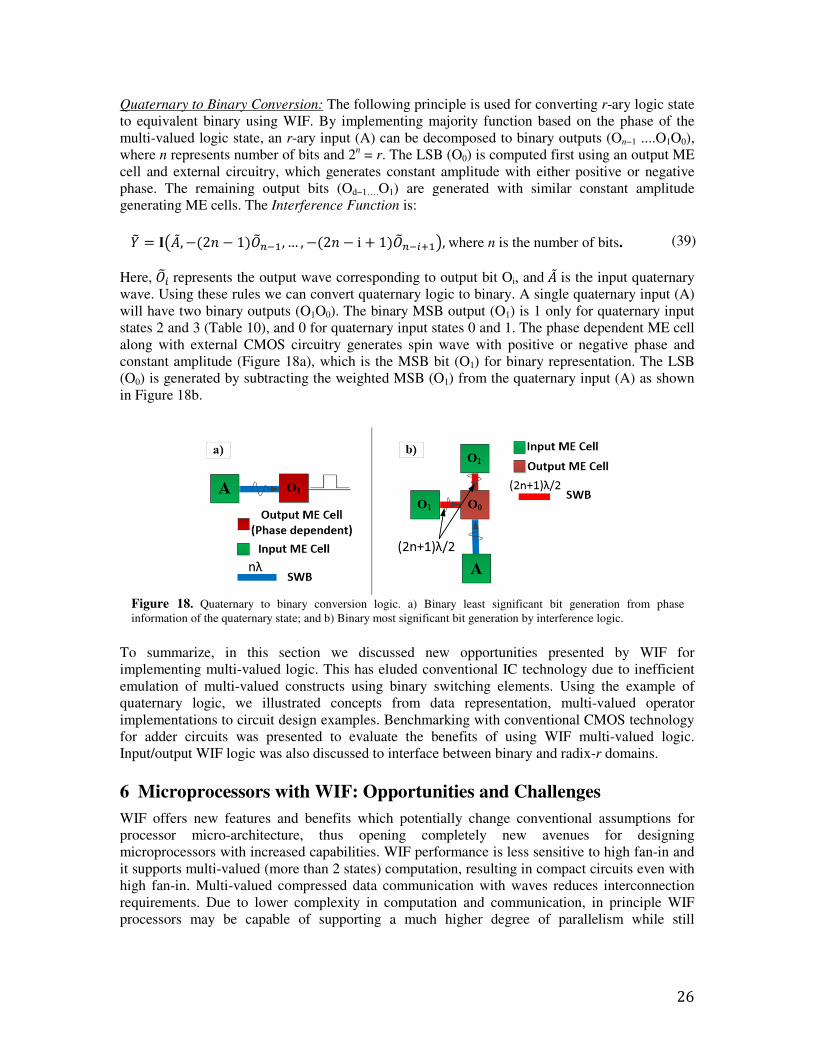
Quaternary to Binary Conversion: The following principle is used for converting r-ary logic state
to equivalent binary using WIF. By implementing majority function based on the phase of the
multi-valued logic state, an r-ary input (A) can be decomposed to binary outputs (On−1 ....O1O0),
where n represents number of bits and 2n = r. The LSB (O0) is computed first using an output ME
cell and external circuitry, which generates constant amplitude with either positive or negative
phase. The remaining output bits (Od−1….O1) are generated with similar constant amplitude
generating ME cells. The Interference Function is:
'� = ��4I, <�2� < 1�y����, … , <�2� < i � 1�y����P� ,where n is the number of bits. (39)
Here, y�� represents the output wave corresponding to output bit Oi, and 4I is the input quaternary
wave. Using these rules we can convert quaternary logic to binary. A single quaternary input (A)
will have two binary outputs (O1O0). The binary MSB output (O1) is 1 only for quaternary input
states 2 and 3 (Table 10), and 0 for quaternary input states 0 and 1. The phase dependent ME cell
along with external CMOS circuitry generates spin wave with positive or negative phase and
constant amplitude (Figure 18a), which is the MSB bit (O1) for binary representation. The LSB
(O0) is generated by subtracting the weighted MSB (O1) from the quaternary input (A) as shown
in Figure 18b.
To summarize, in this section we discussed new opportunities presented by WIF for
implementing multi-valued logic. This has eluded conventional IC technology due to inefficient
emulation of multi-valued constructs using binary switching elements. Using the example of
quaternary logic, we illustrated concepts from data representation, multi-valued operator
implementations to circuit design examples. Benchmarking with conventional CMOS technology
for adder circuits was presented to evaluate the benefits of using WIF multi-valued logic.
Input/output WIF logic was also discussed to interface between binary and radix-r domains.
6 Microprocessors with WIF: Opportunities and Challenges
WIF offers new features and benefits which potentially change conventional assumptions for
processor micro-architecture, thus opening completely new avenues for designing
microprocessors with increased capabilities. WIF performance is less sensitive to high fan-in and
it supports multi-valued (more than 2 states) computation, resulting in compact circuits even with
high fan-in. Multi-valued compressed data communication with waves reduces interconnection
requirements. Due to lower complexity in computation and communication, in principle WIF
processors may be capable of supporting a much higher degree of parallelism while still
Figure 18. Quaternary to binary conversion logic. a) Binary least significant bit generation from phase
information of the quaternary state; and b) Binary most significant bit generation by interference logic.

27
providing an efficient implementation (more than 4-way instruction issue – a limitation of CMOS
technology due to exponential increase in complexity).
WIF memory implementation can be done identical to logic, with grid-based waveguides and
ME-cells for control. This can (i) merge computation with memory leading to a distributed
architecture with a lesser degree of localization for execution and memory units, further reducing
communication requirements; and (ii) potentially surmount the memory-wall problem that
impacts CMOS processors, because WIF logic and memory performance scale identically. It may
lead to a completely different memory
organization than what is seen today. Also,
absence of charge transport for computation
yields orders of magnitude power benefits vs.
CMOS which considerably improves the
performance-per-watt metric, and non-volatility
allows an instant-on processor realization.
While much work is needed to explore all
possibilities with WIF technology, here we
discuss the feasibility and benefits of WIF-
based 8-bit embedded processor [47] vs. CMOS
8-bit AVR processor [50].
The architecture for an WIF 8-bit embedded
processor is shown in Figure 19. We envision
an instant-on processor where the non-volatile
ME cells themselves (capable of latching data)
store the machine state information, without the
need to write back the machine state to a separate memory unit. These non-volatile ME cells also
enable a unified architecture (ALU fused with register file), thus eliminating the need for a
separate register-file. This leads to a significant reduction in area. In addition, the main blocks in
the ALU such as carry look-ahead (CLA) adders are much more efficiently implemented with
WIF. This is because the CLA unit can be implemented in a single stage [47], even at higher bit-
widths. A CMOS implementation uses multiple CLA units for high bit-width adders due to fan-in
limitations (see Figure 20). These factors significantly reduce circuit complexity for WIF
arithmetic circuit implementations and, in conjunction with the fact that there is no charge
transport involved, result in area and power benefits. In addition, memory blocks are non-volatile
Figure 19. WIF 8-bit embedded processor
architecture [47].
Figure 20. Carry look-ahead adder implemented with (a) CMOS; and (b) WIF [47]. In the equations for delay
estimation, Δg – Gate delay based on 45nm Nangate standard cell lib.; N – Number of inputs; B – Blocking factor;
LME – ME cell width; PME – ME cell pitch; MEDelay – ME cell switching delay; VSpin – Propagation velocity of spin
waves; and K – Number of ME cells on critical path.

28
TABLE 11. EMBEDDED WIF PROCESSOR BENCHMARKING
Fabric Processor Logic Core Comparison
Area Power Performance (delay on ALU critical path)
WIF (2µm) 0.3 mm2 0.25mW ~40ns
CMOS (1.5µm) 8 mm2 10mW ~15ns
and can be supported with ME cells organized in a grid waveguide layout with readout at the end
of each row. Some minimal control is necessary in the electrical domain.
Analytical estimation was done for evaluating potential benefits and feasibility of 8-bit WIF
embedded processor [47]. Area of WIF designs was calculated by assuming ME cell dimensions
of 2µm*2µm, based on what can be experimentally achieved currently. Feature size scaling limits
are similar to CMOS since manufacturing will have to rely on lithography for wave guide
creation. The comparison is therefore done with 1.5µm CMOS. Performance/clock speed was
based on critical path analysis of the CLA unit in the ALU, which included ME cell switching
delay and wave propagation delay along the critical path (path with longest delay). The ME cell
was assumed to have a switching delay of 10ns. Spin wave group velocity was assumed to be
104m/s for calculating spin wave propagation delay. Since spin wave propagation does not
involve any charge transport, power consumption for WIF designs are mainly from ME cell
switching activity. Based on numerical simulations and by using a simple capacitor
approximation, ME cell switching energy was estimated to be as low as 3.85fJ per operation for
the feature size used here.
For CMOS, a generic 8-bit processor core [50] was defined in Verilog and synthesized using
Design Compiler with 45nm North Carolina State University (NCSU) Product Development Kit
(PDK). The area, power and delay numbers were calculated from the synthesized designs, and
scaled up to the nearest 1.5µm CMOS technology node (to compare it with equivalent WIF
designs). The following rules were used for CMOS scaling – area was scaled by 2X for every
technology node, the delay was scaled by 30% every generation and the power was scaled by
(VDD scaling)2 [51]. For 45nm technology node, VDD was 0.9V and for 1.5µm it was 5V.
Evaluation results indicate that WIF-based processor may have up to 40x lower power and 27x
smaller area vs. CMOS (see Table 11). While further exploration is necessary, WIF technology
can be game-changing for implementing future microprocessors and embedded systems.
However, additional factors need to be considered to build large-scale processors with WIF. In
addition to patterning functionally correct layouts, careful consideration is also needed to ensure
that spin waves are generated and captured at specific time instants to ensure correct
functionality. Synchronization aspects of WIF designs are closely related to how ME cells operate
to (i) generate new waves, and (ii) capture information from incoming waves. The ME cells
discussed in this chapter are bi-stable devices with an energy separation between the two stable
states. An additional meta-stable state can be used to reduce the amount of energy necessary to
switch the ME cell from one stable state to another. In this meta-stable state, the ME cell is ready
to be switched to either of the stable states based on the phase of the incoming wave. Thereby, a
combination of layout patterning techniques and external electrical control signals can be used to
assure that waves are generated and captured correctly. Here, we discuss this aspect of designing
circuits with WIF using several layout topologies for a WIF 1-bit adder for illustration [16].
Figure 21 shows three different variants of WIF 1-bit adder with different fabric assumptions and
control schemes.

29
The design shown in Figure 21A requires inversion in the spin domain for the Sum output to be
calculated. This is realized by designing the spin wave bus topology to facilitate logic inversion
(using waveguide of length equal to odd multiple of spin wave half-wavelength). This is a custom
layout technique which leads to a highly compact design. However, from a synchronization
perspective we need separate control signals to force intermediate ME cells (I2 cells in Figure 21)
and the Sum output ME cells into meta-stable state, primarily due to layout imbalance between
the paths of the incoming waves that interfere to produce the Sum output. Timing diagrams in
Figure 21A (right) show that two separate external control signals (CLK1, CLK2) are needed for
correct operation of this design.
This requirement on additional clock signals can be mitigated by using balanced layouts. This
would ensure that waves travel equal distance before superposition leading to simplified control
schemes. With this in mind, the adder can be redesigned as shown in Figure 21B and Figure 21C.
In Figure 21B, balancing is achieved by using special waveguides with a pinned magnetic layer.
In comparison with the regular single layer ferromagnetic waveguides, the pinned layer provides
additional phase shift of ‘π’ for the same propagation length. Thereby, a single external clock
signal is sufficient to control both output and intermediate ME cells. However, it requires a new
fabric component to support special waveguides with a pinned magnetic layer. A possible third
alternative is to eliminate intermediate inversions in the design by using dual-rail logic. This logic
style eliminates the need for intermediate inversion by using both ‘true’ and ‘complementary’
inputs as primary inputs and generating both ‘true’ and ‘complementary’ outputs for every
function. The redesigned adder is shown in Figure 21C. This further illustrates the importance of
Figure 21. Different 1-bit WIF adder designs based on synchronization and external control requirements [16]. a)
Custom layout with two separate external control signals. b) Balanced layout with only one external control signal.
This design uses special waveguide with a pinned magnetic layer to enable inversion while still using a balanced
layout. c) Balanced layout based on dual-rail logic without using pinned magnetic layer.

30
an integrated fabric-circuit-layout exploration methodology in such unconventional computing
fabrics.
Another important aspect to consider for large-scale processor designs is the communication
requirements, and the impact of spin wave velocity on communication delay. Evaluation of
transport parameters for spin propagation and electric charge, indicate that spin propagation is
inferior to charge transfer. Experimental results have shown that, the maximum propagation
velocity of spin waves is about 104 m/s [11]. This is considerably slower than the charge
propagation speed in metal interconnects. For example, at 45nm technology node signal delay in
charge domain is about 10ps, while it is about 100ps in spin domain (10X slower) for
interconnect length of 1μm (minimum sized). With increased fan-in, the size of WIF circuits also
increases and may lead to stringent requirements on routing. If the routing length requirements
for spin wave bus cannot be satisfied, then the data encoded by the wave can be corrupted since
wave propagation distance affects both phase and amplitude. Thus, while high fan-in logic may
be efficiently accomplished in the spin domain, we believe that long-range communication is
better accomplished in the charge domain. A hybrid fabric with computation based on patterned
waveguides for spin waves, and interconnects based on conventional CMOS metal routing layers
may benefit from the best of both technologies. In such a fabric, ME cell can provide the essential
interface mechanism to switch between charge and spin domains. Identifying the granularity at
which to switch domains would be an interesting aspect to explore in such hybrid fabrics.
7 Summary and Future Work
Wave Interference Functions (WIF) is a new fully generic computational paradigm for post-
CMOS integrated circuits based on wave-like physical phenomenon. Although spin waves were
used to illustrate this approach, WIF is generic and applicable to any wave phenomenon. Waves
offer new features and opportunities for developing logic circuits, and inherently support compact
multi-valued data representation – each wave attribute with multiple values can be used to
represent data. Information is processed through wave interference with inherent support for
multi-valued operations, resulting in compact logic networks due to compressed data encoding at
the output. Communication between processing elements is achieved through multi-valued wave
propagation which reduces interconnect requirements. Binary and multi-valued WIF circuits
show tremendous benefits when compared to conventional CMOS technology. For instance, a 2-
digit quaternary WIF full adder showed 61x density, 640x lower power and 2.2x performance
advantage vs. CMOS binary 4-bit adder, whereas the 16-digit quaternary WIF full adder showed
63x density, 884x lower power and 3x performance improvement vs. 32-bit CMOS. The
improvement in power consumption and density for WIF circuits are primarily due to extremely
low switching power of ME cells, device-less computation, inherent support for high fan-in
multi-valued logic, compressed logic representation through multi-valued operators, and compact
implementation in WIF fabric. These factors also contribute towards performance improvements.
Large-scale processors that leverage these new features with WIF can be game-changing for
implementing future non-volatile microprocessors and embedded systems. Further exploration is
necessary to enable large-scale implementation using WIF. At the logic design level, algorithms
need to be developed to efficiently express any desired functionality in terms of Interference
Functions. Circuit-level design aspects that need to be explored include noise analysis due to
reflections, attenuation etc., with waves. Large-scale processors may require interfacing between
electrical and magnetic domains to satisfy placement/routing and performance constraints, given
that WIF implementations are sensitive to waveguide lengths and topology. New types of defect
and fault-tolerance techniques may be developed with WIF by leveraging the intrinsic features
and opportunities with multi-valued wave computation.

31
References:
[1] S. Khasanvis, M. Rahman, S. N. Rajapandian, and C. A. Moritz, "Wave-based multi-
valued computation framework," IEEE/ACM Int. Symp. Nanoscale Architectures,
2014, pp. 171-176, July 2014.
[2] S. Datta and B. Das, “Electronic analog of the electro-optic modulator,” Appl. Phys.
Lett., vol. 56, no. 7, pp. 655-667, 1990.
[3] W. R. Dichtel, J. R. Heath and S. J. Fraser, “Designing bistable rotaxanes for molecular
electronic devices,” Philoso. Trans. Roy. Soc. A: Math., Physical and Eng. Sciences,
vol. 365, no. 1855, pp. 1607-1625, June 2007.
[4] J. M. Tour, “Molecular electronics. Synthesis and testing of components,” Accounts of
Chemical Research, vol. 33, pp. 791-804, Aug. 2000.
[5] M. H. R. Lankhorst, B. W. S. M. M. Ketelaars and R. A. M. Wolters, “Low-cost and
nanoscale non-volatile memory concept for future silicon chips,” Nature Materials,
vol. 4, pp. 347-352, Mar. 2005.
[6] C. A. Moritz, T. Wang, P. Narayanan, M. Leuchtenburg, Y. Guo, C. Dezan and M.
Bennaser, “Fault-tolerant nanoscale processors on semiconductor nanowire grids,”
IEEE Trans. Circuits Syst. I, Reg. Papers, vol. 54, no. 11, pp. 2422-2437, Nov. 2007.
[7] D. B. Strukov and K. K. Likharev, “Reconfigurable hybrid CMOS/nanodevice circuits
for image processing,” IEEE Trans. Nanotechnol., vol. 6, no. 6, pp. 696-710, Nov.
2007.
[8] Z. F. Wang, H. Zheng, Q. W. Shi and J. Chen, “Emerging nanocircuit paradigm:
Graphene-based electronics for nanoscale computing,” IEEE Int. Symp. Nanoscale
Architectures, 2007, pp. 93-100, Oct. 2007.
[9] P. L. McEuen, M. S. Fuhrer and H. Park, “Single-walled carbon nanotube electronics,”
IEEE Trans. Nanotechnol., vol. 1, no. 1, pp. 78-85, Mar. 2002.
[10] M. M. Shulaker et al., “Carbon nanotube computer,” Nature, vol. 501, pp. 526–530,
Sep. 2013.
[11] A. Khitun, M. Bao and K. L. Wang, "Spin wave magnetic nanofabric: A new approach
to spin-based logic circuitry," IEEE Trans. on Magn., vol. 44, no. 9, pp. 2141-2152,
Sep. 2008.
[12] P. Shabadi et al., "Towards logic functions as the device," IEEE Int. Symp. Nanoscale
Architectures, 2010, pp. 11-16, June 2010.
[13] P. Shabadi and C. A. Moritz, "Post-CMOS hybrid spin-charge nanofabrics," IEEE
Conf. Nanotechnol., 2011, pp. 1399-1402, Aug. 2011.
[14] P. Shabadi, A. Khitun, K. Wong, P. K. Amiri, K. L. Wang and C. A. Moritz, "Spin
wave functions nanofabric update," IEEE Int. Symp. Nanoscale Architectures, 2011,
pp. 107-113, June 2011.
[15] J. G. Alzate et al., "Spin wave nanofabric update," IEEE Int. Symp. Nanoscale
Architectures, 2012, pp. 196-202, July 2012.
[16] P. Shabadi, S. N. Rajapandian, S. Khasanvis and C. A. Moritz, “Design of spin wave
functions-based logic circuits,” SPIN, vol. 2, no. 3, Article 1240006, World Scientific
Publishing Company, 2012.
[17] T. Schneider, A. A. Serga, B. Leven, B. Hillebrands, R. L. Stamps and M. P. Kostylev,
“Realization of Spin Logic Gates,” Appl. Phys. Lett., vol. 92, no. 2, p. 022505, Jan.
2008.
[18] M. Covington, T. M. Crawford and G. J. Parker, “Time-resolved measurement of
propagating spin waves in ferromagnetic thin films,” Phys. Rev. Lett., vol. 89, p.
237202, Nov. 2002.
[19] M. P. Kostylev, A. A. Serga, T. Schneider, B. Leven and B. Hillebrands, “Spin-wave
logical gates,” Appl. Phys. Lett., vol. 87, no. 15, p. 153501, Oct. 2005.

32
[20] Stancil, Daniel D, and Anil Prabhakar, Spin Waves: Theory and Applications. New
York, NY: Springer, 2009.
[21] M. Bailleul, D. Olligs and C. Fermon, “Propagating spin wave spectroscopy in a
permalloy film: A quantitative analysis,” Appl. Phys. Lett., vol. 83, no. 5, pp. 972-974,
Aug. 2003.
[22] M. Bao et al., “Determining wave vector and material property from the phase-shift of
spin-wave propagation,” Europhysics Letters, vol. 84, no. 2, p. 27009, Oct. 2008.
[23] P. K. Amiri, B. Rejaei, M. Vroubel and Y. Zhuang, “Nonreciprocal spin wave
spectroscopy of thin Ni-Fe stripes,” Appl. Phys. Lett., vol. 91, no. 6, p. 062502, Aug.
2007.
[24] W. Eerenstein, N.D. Mathur and J. F. Scott, “Multiferroic and magnetoelectric
materials,” Nature, vol. 442, pp. 759-765, Aug. 2006.
[25] G. Srinivasan, E. T. Rasmussen, J. Gallegos, R. Srinivasan, I. Bokhan Yu and V. M.
Laletin, “Magnetoelectric bilayer and multilayer structures of magnetostrictive and
piezoelectric oxides,” Phys. Rev. B, vol. 64, pp. 214408, Nov. 2001.
[26] J. V. D. Boomgaard, D. R. Terrell, R. A. J. Born and H. Giller, “An in situ grown
eutectic magnetoelectric composite material,” J. Mater. Sci., vol. 9, pp. 1705-1709,
Oct. 1974.
[27] R. Jungho, V. Carazo, K. Uchino and K. Hyoun-Ee, “Magnetoelectric properties in
piezoelectric and magnetostrictive laminate composites,” Jpn. J. Appl. Phys., vol. 40,
part 1 no. 8, pp. 4948-4951, Aug. 2001.
[28] W. Yu, J. A. Bain, W. C. Uhlig and J. Unguris, “The effect of stress-induced anisotropy
in patterned FeCo thin-film structures,” J. Appl. Phys., vol. 99, no. 8, p. 8B706, Apr.
2006.
[29] S. Cherepov et al., "Electric-field-induced spin wave generation using multiferroic
magnetoelectric cells," Appl. Phys. Lett., vol. 104, no. 8, pp. 082403, Feb. 2014.
[30] A. Khitun, D. E. Nikonov and K. L. Wang, “Magnetoelectric spin wave amplifier for
spin wave logic circuits,” J. Appl. Phy., vol. 106, no. 12, p. 123909, Dec. 2009.
[31] Y. V. Kornyushin, "Amplification of Magnetization Waves in Ferromagnetic
Conductors," Physica Status Solidi (b), vol. 41, no. 1, pp. 265-269, Jan. 1970.
[32] B. A. Kalinikos, M. K. Kovaleva, and N. G. Kovshikov, USSR Patent, USSR No.
778606, Otkrytiya, Izobret, no. 26, p. 225, 1988.
[33] G. A. Melkov and S. V. Sholom, “Amplification of surface magnetostatic waves by a
parametric pump”, Zhurnal Tekhnicheskoi Fiziki, no. 60, pp. 118-23, 1990.
[34] K. R. Smith, V. I. Vasyuchka, W. Mingzhong, G. A. Melkov and C. E. Patton,
"Cloning and trapping of magnetostatic spin-wave pulses by parametric pumping,"
Phys. Rev. B, vol. 76, pp. 054412, Aug. 2007.
[35] B. A. Kalinikos, N. G. Kovshikov, M. P. Kostylev, P. Kabos and C. E. Patton,
"Observation of the amplification of spin-wave envelope solitons in ferromagnetic
films by parallel magnetic pumping," J. Experimental and Theoretical Phys. Lett., vol.
66, no. 5, pp. 371-375, Sep. 1997.
[36] M. Bao, A. Khitun, W. Yina, L. Joo-Young, K. L. Wang and A. P. Jacob, "Coplanar
waveguide radio frequency ferromagnetic parametric amplifier," Appl. Phys. Lett., vol.
93, no. 7, p. 072509, Aug. 2008.
[37] S. Amarel, G. Cooke and R. O. Winder, "Majority Gate Networks," IEEE Trans.
Electronic Computers, vol. EC-13, no.1, pp. 4-13, Feb. 1964.
[38] I. Koren, Computer Arithmetic Algorithms, 2nd ed. Natick, MA: A. K. Peters, 2002.
[39] C. M. Allen and D. D. Givone, “A minimization technique for multiple-valued logic
systems,” IEEE Trans. Computers, vol. C-17, no. 2, pp. 182-184, Feb. 1968.
[40] D. M. Miller and M. A. Thornton, Multiple valued logic: Concepts and
representations. San Rafael, Calif.: Morgan & Claypool Publishers, 2008.

33
[41] Z. G. Vranesic, E. S. Lee and K. C. Smith, "A many-valued algebra for switching
systems," IEEE Trans. Computers, vol. C-19, no.10, pp. 964-971, Oct. 1970.
[42] P. P. Tirumalai and J. T. Butler, "Prime and non-prime implicants in the minimization
of multiple-valued logic functions," IEEE Int. Symp. Multiple-Valued Logic, 1989, pp.
272-279, 1989.
[43] J. Yunjian and R. K. Brayton, "Don't cares and multi-valued logic network
minimization," IEEE Int. Conf. Computer Aided Design, 2000, pp. 520-525, Nov.
2000.
[44] S. P. Onneweer and H. G. Kerkhoff, “High-radix current-mode CMOS circuits based
on the truncated difference operator,” IEEE Int. Symp. Multiple-Valued Logic, 1987,
pp. 188-195, 1987.
[45] T. Temel and A. Morgul, “Implementation of multi-valued logic, simultaneous literal
operations with full CMOS current-mode threshold circuits,” Electronics Letters, vol.
38, no. 4, pp. 160-161, Feb. 2002.
[46] T. Temel and A. Morgul, “Implementation of multi-valued logic gates using full
current-mode CMOS circuits,” Analog Integrated Circuits and Signal Processing,
Kluwer Academic Publishers, vol. 39, no. 2, pp. 191-204, May 2004.
[47] S. Khasanvis, S. N. Rajapandian, P. Shabadi, J. Shi and C. A. Moritz, "Embedded
processors based on Spin Wave Functions (SPWFs)," IEEE Int. Symp. Nanoscale
Architectures, 2013, pp. 32-33, July 2013.
[48] S. Rakheja, A. Naeemi and J. D. Meindl, “Physical limitations on delay and energy
dissipation of interconnects for post-CMOS devices,” IEEE Int. Interconnect
Technology Conference, 2010, pp. 1-3, June 2010.
[49] P. Shabadi and C. A. Moritz, "Post-CMOS hybrid spin-charge nanofabrics," IEEE
Conf. Nanotechnol., 2011, pp. 1399-1402, Aug. 2011.
[50] Atmel Corporation, "8-bit Atmel Microcontroller with 128KBytes In-System
Programmable Flash," ATMEGA128L Datasheet, Jun. 2011. [Online] Retrieved May
31, 2014 from http://www.atmel.com/Images/doc2467.pdf
[51] S. Borkar, "Design challenges of technology scaling," IEEE Micro, vol. 19, no. 4, pp.
23-29, Jul-Aug 1999.