Embed Size (px)
Citation preview

ULPFA: A New Efficient Design of
a Power-Aware Full Adder
ByM.V.Mounika,14204116.

Introduction
• The choice of logic style to design digital circuits strongly
influences the circuit performance.
• The delay time depends on the size of transistors, the number
of transistors per stack, the parasitic capacitance including
intrinsic capacitance and capacitance due to intracell and
intercell routing, and the logic depth (i.e., number of logic
gates in the critical path).

• The dynamic power consumption depends on the switching
activity and the number and size of transistors (i.e., their
contribution)
• Although dynamic power is continuously being reduced with
technology scaling, static leakage power tends to increase and
is expected to become a large contributor to total power in a
few technology generationto parasitic capacitances).
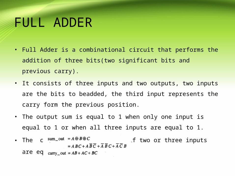
FULL ADDER
• Full Adder is a combinational circuit that performs the addition of three
bits(two significant bits and previous carry).
• It consists of three inputs and two outputs, two inputs are the bits to
beadded, the third input represents the carry form the previous position.
• The output sum is equal to 1 when only one input is equal to 1 or when all
three inputs are equal to 1.
• The cout output has a carry 1 if two or three inputs are equal to 1.
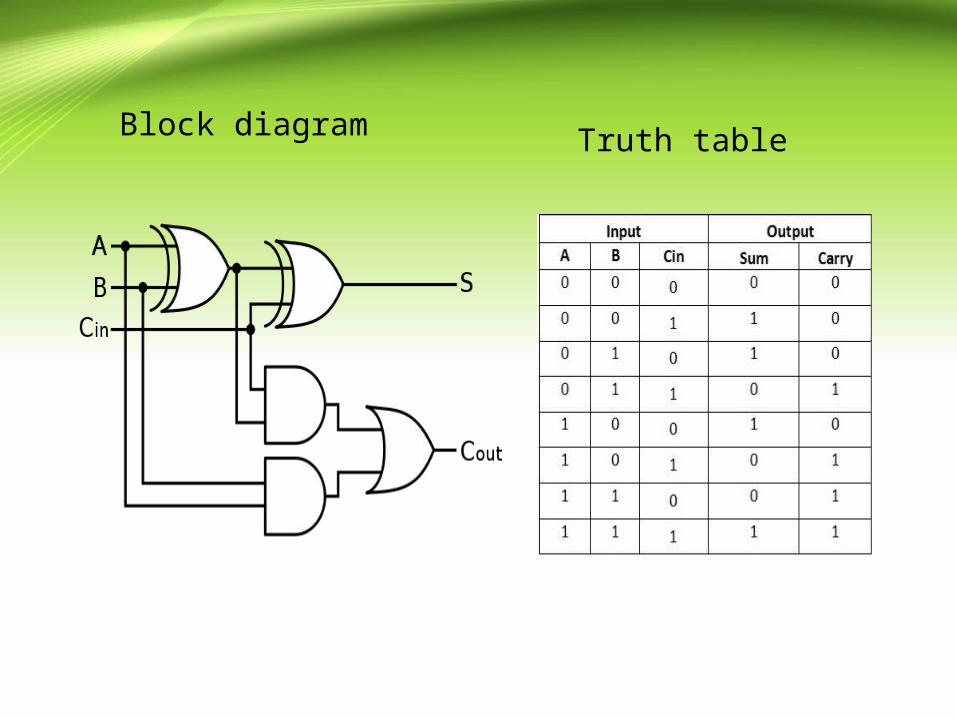
Block diagram Truth table

BBL-PT Full Adder
Sum circuit Carry circuit

• In branch-based design, some constraints are applied to the nMOS and
pMOS networks. In fact, the networks are composed only of branches,
i.e., series connections of transistors between the output node and the
supply rail.
• The disadvantage of this implementation lies in the resulting weak high
output level in pass transistors used in the sum block of the proposed full
adder
• Power dissipation:322.214pw
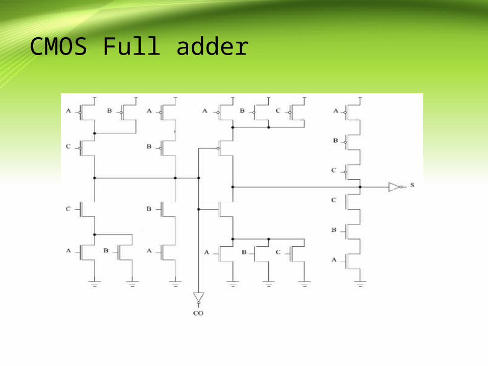
CMOS Full adder

The sum out and carry-out signals can be found as the
following two combinational Boolean functions of the three input
variables, A, B and C.
we use the carry-out signal to generate the sum output, since
the output can also be expressed as

• This adder was based on regular CMOS structure (pull-up and pull-down
network) (Fig 2).
• Working principle: Cout is generated first using AB+BC+AC. Then the
sum is derived from the sum using carry output.
• Advantages: One of the most significant advantages of this full adder was
its high noise margins and thus reliable operation at low voltages.
• Disadvantages: But the use of substantial number of transistors results in
high input loads, more power consumption and larger silicon area.
• Power dissipation:36.45pw
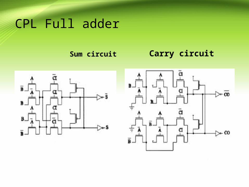
CPL Full adder
Sum circuit Carry circuit

• The complementary pass-transistor logic (CPL) full adder has 32 transistors and is
based on the CPL logic.
• CPL full adder provides high-speed, full-swing operation and good driving
capabilities due to the output static inverters and fast differential stage of cross
coupled PMOS transistors
• The disadvantage, of pass transistor logic is that Threshold voltage drops through
the NMOS transistors makes it necessary to maintain output voltage level, as a
result inverter is used at output which increases the number of transistors and
power dissipation is more.
• power dissipation:389.799nw

Hybrid Full adder
Sum circuit Carry circuit
• In order to prevent the voltage step that appears in 0 1 transitions on the
sum output signal, and to reduce dynamic power (which is impaired by the
large drain and gate capacitance on the “Sout” node due to the level
restorer), further optimization has been carried out on the sum block of the
hybrid FA. We implement hereafter the sum block with LP XOR and
XNOR gates.
• Power dissipation :90.888fw

ULP Full adder
Sum circuit Carry circuit
• Ultra low power full adder based on the low power XOR (LP-XOR) gate
and ultra low power devices (ULPD).
• It features a strongly reduced leakage current when compared to a standard
diode-connected MOSFET while maintaining similar forward current drive
capability.
•The ULPD is obtained by the combination of an nMOS and pMOS transistor.
•Advantage: leakage power is reduced.
•power dissipation:8.56fw
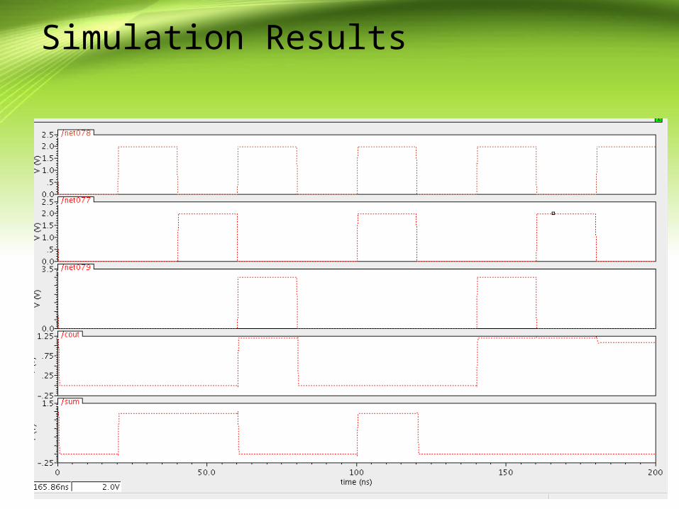
Simulation Results

Applications
• Implementations of microprocessors.
• ALUs and multipliers.
• Particularly for digital signal processors in embedded
applications where high-processing-speed capability must
cope with LP management

Conclusion
• In this project, we have presented a new hybrid structure of a
full adder. Its optimization has been carried out to further
lower total and static powers
04/15/23


