Embed Size (px)
Citation preview
SDSoC Environment Tutorial
Platform Creation
UG1236 (v2017.4) January 26, 2018

Table of ContentsRevision History...............................................................................................................5
Chapter 1: SDSoC Platform Creation Tutorial................................................. 7Hardware and Software Requirements.................................................................................... 7Tutorial Design Descriptions......................................................................................................7Locating Tutorial Design Files....................................................................................................9
Chapter 2: Lab 1: Creating DSA for a Zynq-7000 AP SoC ProcessorDesign............................................................................................................................. 11Step 1: Start the Vivado IDE and Create a Project.................................................................11Step 2: Create an IP Integrator Design...................................................................................13Step 3: Setting Platform Properties........................................................................................ 26Step 4: Generating HDL Design Files...................................................................................... 28Step 5: Writing Out the DSA.....................................................................................................29Conclusion..................................................................................................................................29Lab Files...................................................................................................................................... 30
Chapter 3: Lab 2: Creating Software Components for thePlatform.........................................................................................................................31Step 1: Launching SDK..............................................................................................................31Step 2: Creating an FSBL Application......................................................................................32Step 3: Generating the Boot Image File (BIF)........................................................................ 35Step 4: Creating a New Software Application and a Linker Script.......................................38Step 5: Copying and Editing Files............................................................................................ 43Conclusion..................................................................................................................................44Lab Files...................................................................................................................................... 44
Chapter 4: Lab 3: Creating a Custom Platform Using the SDx IDE....45Step 1: Invoking the SDx IDE and Creating a Project............................................................45Step 2: Defining System Configuration.................................................................................. 47Step 3: Adding Processor Domain...........................................................................................48Step 4: Generating the Platform............................................................................................. 50
3UG1236 (v2017.4) January 26, 2018 www.xilinx.com [placeholder text]Send Feedback
Step 5: Adding Custom Platform to Repository.....................................................................51Step 6: Creating an SDx Application Targeting the Custom Platform................................ 52Conclusion..................................................................................................................................57Lab Files...................................................................................................................................... 58
Appendix A: Additional Resources and Legal Notices............................. 59References..................................................................................................................................59Please Read: Important Legal Notices................................................................................... 60
4UG1236 (v2017.4) January 26, 2018 www.xilinx.com [placeholder text]Send Feedback
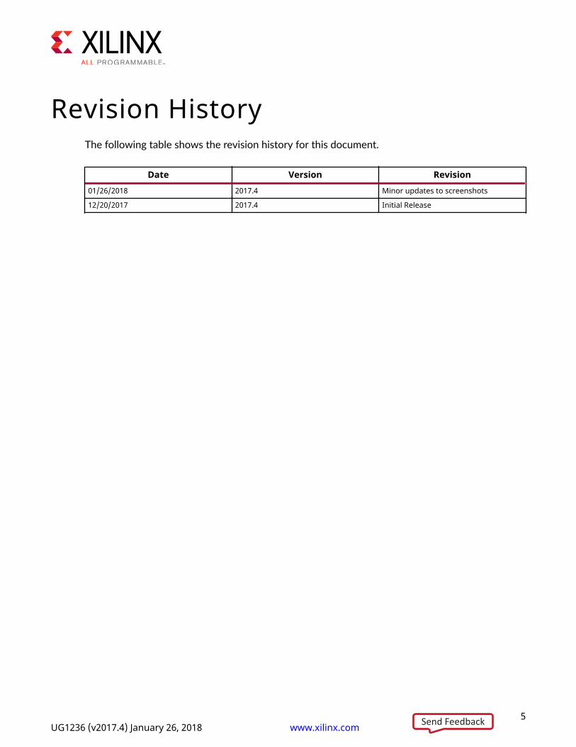
Revision HistoryThe following table shows the revision history for this document.
Date Version Revision01/26/2018 2017.4 Minor updates to screenshots
12/20/2017 2017.4 Initial Release
5UG1236 (v2017.4) January 26, 2018 www.xilinx.com [placeholder text]Send Feedback

Revision History
6UG1236 (v2017.4) January 26, 2018 www.xilinx.com [placeholder text]Send Feedback
Chapter 1
SDSoC Platform Creation TutorialThis tutorial shows how to create an SDSoC™ platform that can be used to accelerate softwarefunctions using the SDx™ Integrated Design Environment (IDE) tool. An SDSoC platform definesa base hardware and software architecture and application context, including processing system,external memory interfaces, custom input/output, and software runtime - including operatingsystem (possibly "bare metal"), boot loaders, drivers for platform peripherals and root file system.Every project you create within the SDx environment Integrated Design Environment (IDE)targets a specific hardware platform, and you employ the tools within the SDx IDE to customizethe platform application-specific hardware accelerators and data motion networks. In this way,you can easily create highly tailored application-specific systems-on-chip for different platforms,and can resue platforms for many different application-specific systems-on-chip.
In this tutorial, you use the Vivado® Design Suite to build a hardware system, and create aplatform using the software runtime environment, including an operating system kernel, bootloaders, file system, and libraries.
Hardware and Software RequirementsThis tutorial requires that you have the SDx Integrated Design Environment installed. See theSDx Environments Release Notes, Installation, and Licensing Guide (UG1238) for instructions. TheSDx tool installs the SDx IDE as well as the required Vivado Design Suite and SoftwareDevelopment Kit (SDK) software.
Tutorial Design DescriptionsNo design files are required for these labs, if step-by-step instructions are followed as outlined;however, for subsequent iterations of the design or to build the design quickly, Tcl command filesfor these labs are provided in the zip file in Locating Tutorial Design Files. For cross-probinghardware and software, manual interaction with Vivado® and Platform boards is necessary. NoTcl files are provided for that purpose.
In this tutorial, users will be guided step-by-step through a series of three labs where:
7UG1236 (v2017.4) January 26, 2018 www.xilinx.com [placeholder text]Send Feedback

1. A Device Support Archive (DSA) is created to define the hardware component for theplatform.
2. A First Stage Boot Loader (FSBL), Boot Image File (BIF), and Linker Script are created todefine the software components for the platform.
3. Finally, the hardware and software components are tied together in the SDx IDE to create aSDx Platform.
Lab 1: Creating DSA for a Zynq-7000 AP SoC Processor Design
Chapter 2: Lab 1: Creating DSA for a Zynq-7000 AP SoC Processor Design uses theZynq®-7000 AP SoC Processing System (PS) IP, and a Clocking Wizard IP to generate severalclocks for potential use in the DSA. Multiple Processor System Reset blocks are used tosynchronize the resets to these different clock sources. The Lab uses the following IP in theProgrammable Logic (PL):
• Clocking Wizard
• Processor System Reset
• ZYNQ7 Processing System
• Concat
Lab 1 shows how to graphically build a design in the Vivado® IP integrator and use the DesignerAssistance feature to configure and connect the Zynq processor to the available interfaces on theZC702 board. Clocking Wizard and Processor System Reset blocks are then added andconnected to complete the design.
After you construct a design, you add properties to the design using Tcl to encapsulate hardware-related information needed to create an SDSoC platform. Finally, the Device Support Archive(DSA) is written.
The lab1.tcl design files are included in the zip file for this guide
See Locating Tutorial Design Files.
Lab 2: Creating Software Components for the Platform in SDK
Chapter 3: Lab 2: Creating Software Components for the Platform requires that you have theSoftware Development Kit (SDK) software installed on your machine.
In Lab 2, you use the SDK software to build the boot image, the Boot Image File (BIF), First StageBoot Loader (FSBL), and the Linker Script file that are needed to create a platform.
If users want to skip over the SDK portion of the lab (Lab 2), four files are provided to the userfor use in Lab 3. These files are:
• BOOT.bin
Chapter 1: SDSoC Platform Creation Tutorial
8UG1236 (v2017.4) January 26, 2018 www.xilinx.com [placeholder text]Send Feedback
• fsbl.elf
• lscript.ld
• standalone.bif
Lab 3: Creating a Custom Platform Using the SDx IDE
In this lab you use the SDx™ IDE to create a platform that uses the DSA you created in Lab 1 andthe software components you created in Lab 2, and then generate the platform. The platform isthen added to the SDx workspace so new applications can be targeted to it.
No design files are provided for this step as the intent is for you to use the SDx IDE to generatethe platform.
Locating Tutorial Design FilesDesign data is in the associated Reference Design File.
Chapter 1: SDSoC Platform Creation Tutorial
9UG1236 (v2017.4) January 26, 2018 www.xilinx.com [placeholder text]Send Feedback

Chapter 1: SDSoC Platform Creation Tutorial
10UG1236 (v2017.4) January 26, 2018 www.xilinx.com [placeholder text]Send Feedback
Chapter 2
Lab 1: Creating DSA for a Zynq-7000AP SoC Processor Design
In this lab you create a Zynq®-7000 AP SoC processor-based design and instantiate IP in theprogrammable logic (PL) to complete your design. Then you set properties on the block design toidentify, clocks, resets, interrupts, and so forth, and finally write out the Device Support Archive(DSA). The custom hardware platform created in this lab has been targeted to a ZC702 platform,although it is not necessary that a predefined board in Vivado® be used to create the DSA.
If you are not familiar with the Vivado Integrated Development Environment (IDE), see theVivado Design Suite User Guide: Using the Vivado IDE (UG893).Note: You can use the Tcl file lab1.tcl that is included with this tutorial design files to perform all the stepsin this lab. To use the Tcl script, launch Vivado and type source lab1.tcl in the Tcl console.
Step 1: Start the Vivado IDE and Create aProject1. Start the Vivado® Design Suite IDE by clicking the Vivado desktop icon. You can also start
Vivado by selecting the Start menu of your computer. Vivado can also be launched from acommand prompt by sourcing the settings file by typing C:\Xilinx\SDx\<sdx version>\settings64.bat. Then you can type vivado at the prompt to launch Vivado.
2. From the Quick Start section, click Create Project, as shown in the the following figure:
11UG1236 (v2017.4) January 26, 2018 www.xilinx.com [placeholder text]Send Feedback

Figure 1: Vivado Quick Start Page
The New Project wizard opens.
Figure 2: Create New Project Wizard
3. Click Next.
The Project Name page opens.
4. In the Project Name page, type the project name zynq7_board and select a location for theproject files. Ensure that the Create project subdirectory check box is checked, and then clickNext.
5. In the Project Type page, select RTL Project, and then click Next.
Chapter 2: Lab 1: Creating DSA for a Zynq-7000 AP SoC Processor Design
12UG1236 (v2017.4) January 26, 2018 www.xilinx.com [placeholder text]Send Feedback
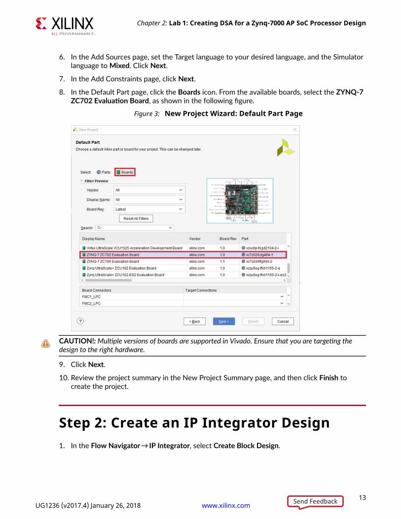
6. In the Add Sources page, set the Target language to your desired language, and the Simulatorlanguage to Mixed. Click Next.
7. In the Add Constraints page, click Next.
8. In the Default Part page, click the Boards icon. From the available boards, select the ZYNQ-7ZC702 Evaluation Board, as shown in the following figure.
Figure 3: New Project Wizard: Default Part Page
CAUTION!: Multiple versions of boards are supported in Vivado. Ensure that you are targeting thedesign to the right hardware.
9. Click Next.
10. Review the project summary in the New Project Summary page, and then click Finish tocreate the project.
Step 2: Create an IP Integrator Design1. In the Flow Navigator → IP Integrator, select Create Block Design.
Chapter 2: Lab 1: Creating DSA for a Zynq-7000 AP SoC Processor Design
13UG1236 (v2017.4) January 26, 2018 www.xilinx.com [placeholder text]Send Feedback
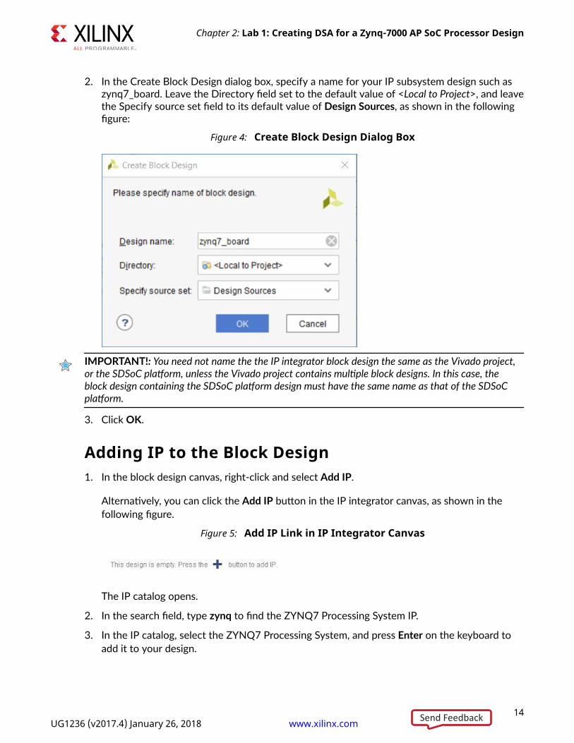
2. In the Create Block Design dialog box, specify a name for your IP subsystem design such aszynq7_board. Leave the Directory field set to the default value of <Local to Project>, and leavethe Specify source set field to its default value of Design Sources, as shown in the followingfigure:
Figure 4: Create Block Design Dialog Box
IMPORTANT!: You need not name the the IP integrator block design the same as the Vivado project,or the SDSoC platform, unless the Vivado project contains multiple block designs. In this case, theblock design containing the SDSoC platform design must have the same name as that of the SDSoCplatform.
3. Click OK.
Adding IP to the Block Design1. In the block design canvas, right-click and select Add IP.
Alternatively, you can click the Add IP button in the IP integrator canvas, as shown in thefollowing figure.
Figure 5: Add IP Link in IP Integrator Canvas
The IP catalog opens.
2. In the search field, type zynq to find the ZYNQ7 Processing System IP.
3. In the IP catalog, select the ZYNQ7 Processing System, and press Enter on the keyboard toadd it to your design.
Chapter 2: Lab 1: Creating DSA for a Zynq-7000 AP SoC Processor Design
14UG1236 (v2017.4) January 26, 2018 www.xilinx.com [placeholder text]Send Feedback

In the Tcl Console, you see the following message:
create_bd_cell -type ip -vlnv xilinx.com:ip:processing_system7:5.5processing_system7_0
The following figure shows the Zynq7 processing system diagram that shows in the IPintegrator canvas.
Figure 6: Zynq7 Processing System IP
There is a corresponding Tcl command for most actions performed in the IP integrator blockdesign. Those commands are not shown in this document; instead, the tutorial provides Tclscripts to run this lab.
Note: Tcl commands are documented in the Vivado Design Suite: Tcl Command Reference Guide (UG8835).
4. In the IP integrator window, click the Run Block Automation link, shown in the followingfigure.
Figure 7: Run Block Automation link
The Run Block Automation dialog box opens, as shown in the below figure. This dialog boxstates that the FIXED_IO and DDR interfaces will be created for the Zynq®-7000 AP SoC IPcore. The Apply Board Preset field is also checked by default.
Chapter 2: Lab 1: Creating DSA for a Zynq-7000 AP SoC Processor Design
15UG1236 (v2017.4) January 26, 2018 www.xilinx.com [placeholder text]Send Feedback
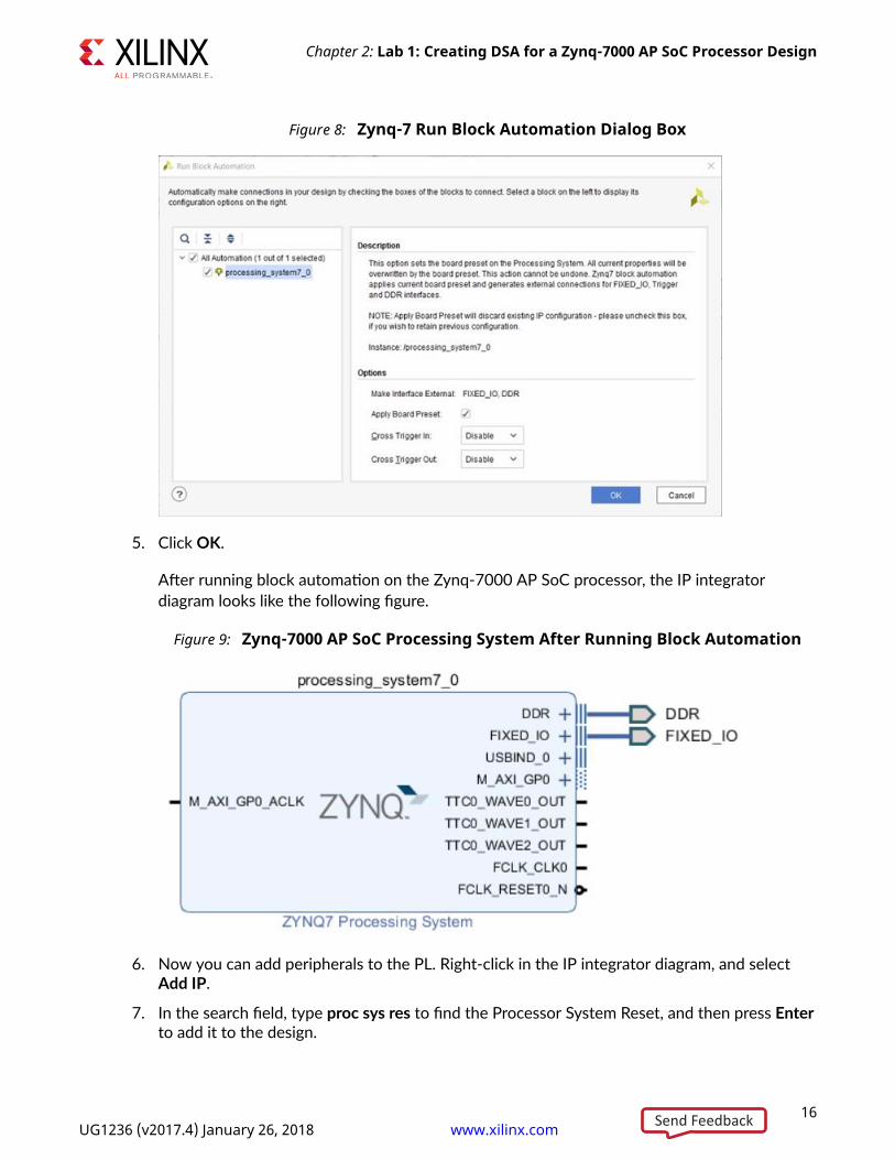
Figure 8: Zynq-7 Run Block Automation Dialog Box
5. Click OK.
After running block automation on the Zynq-7000 AP SoC processor, the IP integratordiagram looks like the following figure.
Figure 9: Zynq-7000 AP SoC Processing System After Running Block Automation
6. Now you can add peripherals to the PL. Right-click in the IP integrator diagram, and selectAdd IP.
7. In the search field, type proc sys res to find the Processor System Reset, and then press Enterto add it to the design.
Chapter 2: Lab 1: Creating DSA for a Zynq-7000 AP SoC Processor Design
16UG1236 (v2017.4) January 26, 2018 www.xilinx.com [placeholder text]Send Feedback
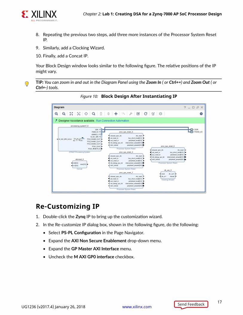
8. Repeating the previous two steps, add three more instances of the Processor System ResetIP.
9. Similarly, add a Clocking Wizard.
10. Finally, add a Concat IP.
Your Block Design window looks similar to the following figure. The relative positions of the IPmight vary.
TIP: You can zoom in and out in the Diagram Panel using the Zoom In ( or Ctrl+=) and Zoom Out ( orCtrl+-) tools.
Figure 10: Block Design After Instantiating IP
Re-Customizing IP1. Double-click the Zynq IP to bring up the customization wizard.
2. In the Re-customize IP dialog box, shown in the following figure, do the following:
• Select PS-PL Configuration in the Page Navigator.
• Expand the AXI Non Secure Enablement drop-down menu.
• Expand the GP Master AXI Interface menu.
• Uncheck the M AXI GP0 interface checkbox.
Chapter 2: Lab 1: Creating DSA for a Zynq-7000 AP SoC Processor Design
17UG1236 (v2017.4) January 26, 2018 www.xilinx.com [placeholder text]Send Feedback
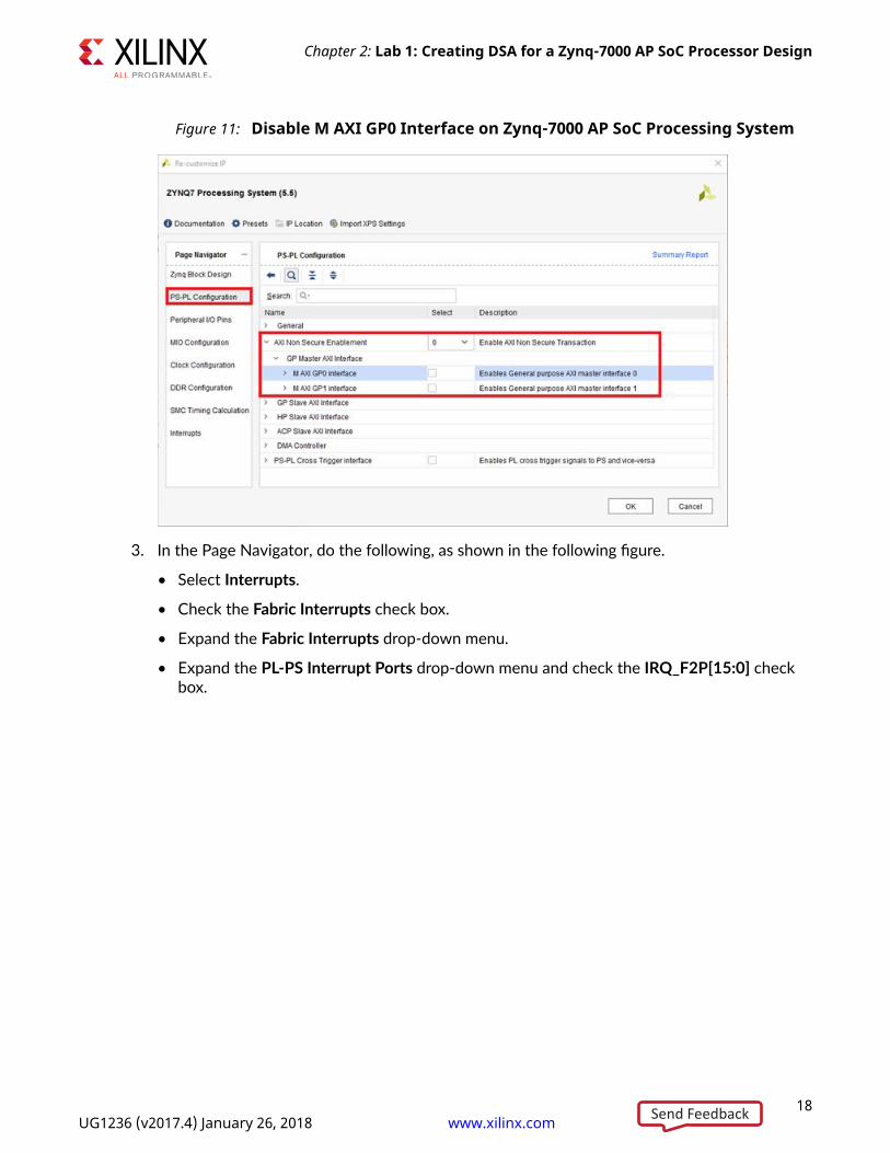
Figure 11: Disable M AXI GP0 Interface on Zynq-7000 AP SoC Processing System
3. In the Page Navigator, do the following, as shown in the following figure.
• Select Interrupts.
• Check the Fabric Interrupts check box.
• Expand the Fabric Interrupts drop-down menu.
• Expand the PL-PS Interrupt Ports drop-down menu and check the IRQ_F2P[15:0] checkbox.
Chapter 2: Lab 1: Creating DSA for a Zynq-7000 AP SoC Processor Design
18UG1236 (v2017.4) January 26, 2018 www.xilinx.com [placeholder text]Send Feedback

Figure 12: Enable Interrupts on Zynq-7000 AP SoC Processing System
4. Click OK.
Next, you re-customize the Clocking Wizard IP, as shown in the following figure.
5. Double-click the Clocking Wizard IP to bring up the customization dialog box.
6. In the Clocking Options tab of the Re-customize IP dialog box, click the Input Frequencycheck box for Primary Clock and change the value in the adjacent box to 50.000.
Figure 13: Change Input Frequency of the Primary Input Clock
Chapter 2: Lab 1: Creating DSA for a Zynq-7000 AP SoC Processor Design
19UG1236 (v2017.4) January 26, 2018 www.xilinx.com [placeholder text]Send Feedback
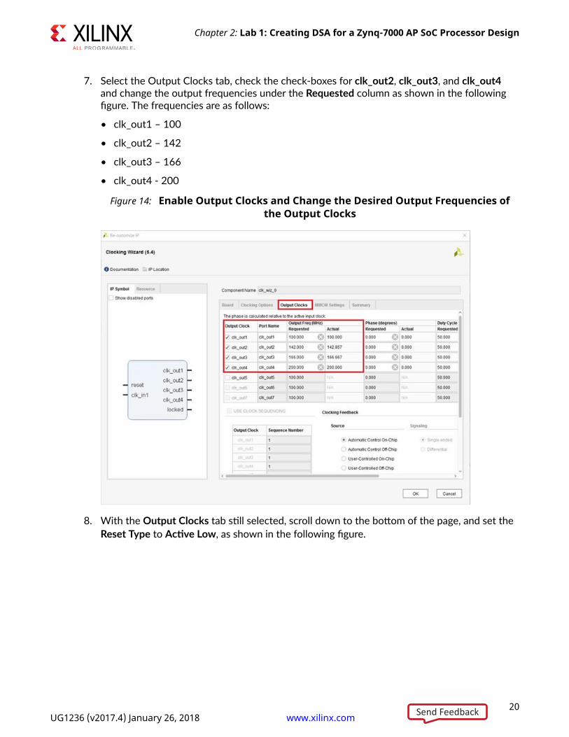
7. Select the Output Clocks tab, check the check-boxes for clk_out2, clk_out3, and clk_out4and change the output frequencies under the Requested column as shown in the followingfigure. The frequencies are as follows:
• clk_out1 – 100
• clk_out2 – 142
• clk_out3 – 166
• clk_out4 - 200
Figure 14: Enable Output Clocks and Change the Desired Output Frequencies ofthe Output Clocks
8. With the Output Clocks tab still selected, scroll down to the bottom of the page, and set theReset Type to Active Low, as shown in the following figure.
Chapter 2: Lab 1: Creating DSA for a Zynq-7000 AP SoC Processor Design
20UG1236 (v2017.4) January 26, 2018 www.xilinx.com [placeholder text]Send Feedback

Figure 15: Change Reset Type
9. Click OK to close the Re-Customize IP dialog box for the Clocking Wizard IP.
10. Double-click the Concat IP to open the Re-customize IP dialog box.
11. Change the Number of Ports field to 1, as shown in the following figure.
Chapter 2: Lab 1: Creating DSA for a Zynq-7000 AP SoC Processor Design
21UG1236 (v2017.4) January 26, 2018 www.xilinx.com [placeholder text]Send Feedback
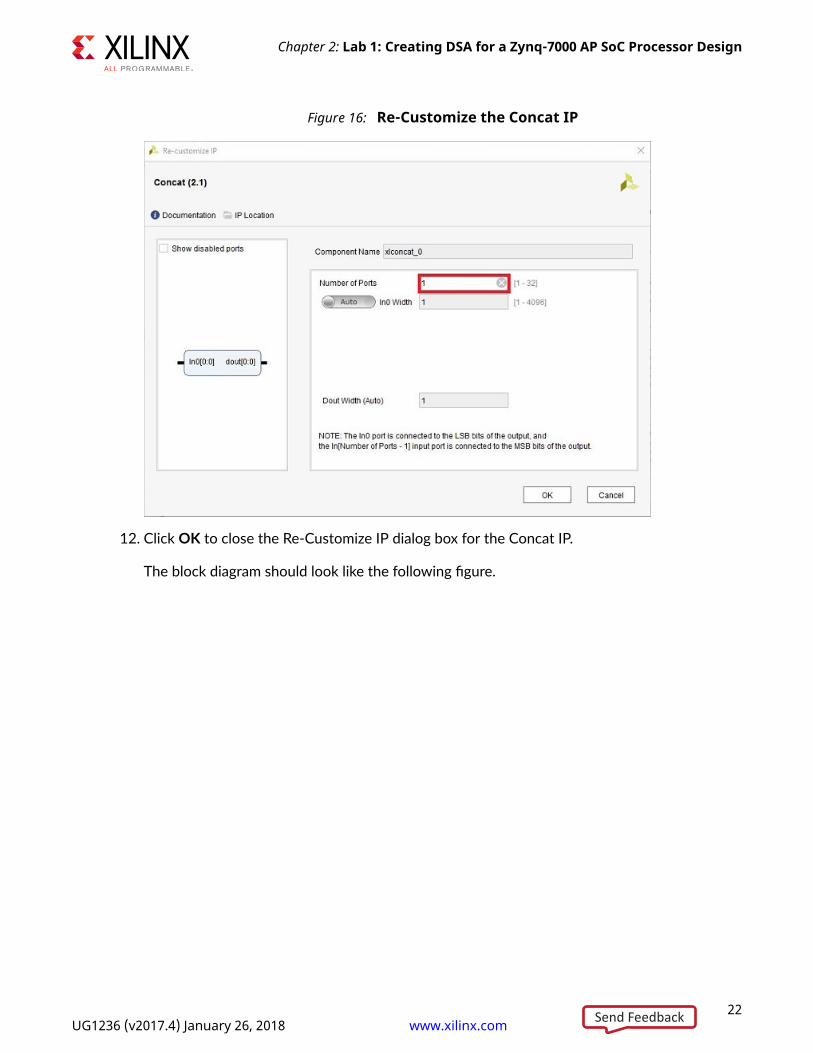
Figure 16: Re-Customize the Concat IP
12. Click OK to close the Re-Customize IP dialog box for the Concat IP.
The block diagram should look like the following figure.
Chapter 2: Lab 1: Creating DSA for a Zynq-7000 AP SoC Processor Design
22UG1236 (v2017.4) January 26, 2018 www.xilinx.com [placeholder text]Send Feedback
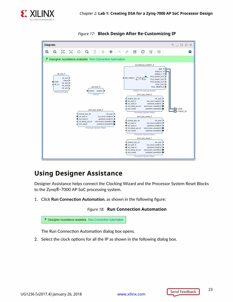
Figure 17: Block Design After Re-Customizing IP
Using Designer AssistanceDesigner Assistance helps connect the Clocking Wizard and the Processor System Reset Blocksto the Zynq®-7000 AP SoC processing system.
1. Click Run Connection Automation, as shown in the following figure:
Figure 18: Run Connection Automation
The Run Connection Automation dialog box opens.
2. Select the clock options for all the IP as shown in the following dialog box.
Chapter 2: Lab 1: Creating DSA for a Zynq-7000 AP SoC Processor Design
23UG1236 (v2017.4) January 26, 2018 www.xilinx.com [placeholder text]Send Feedback

Figure 19: Run Connection Automation Options
As you select each interface for which connection automation is to be run, the descriptionand options available for that interface appear in the right pane.
3. Ensure that all the automation options are set as follows:
Connection More Information Settingclk_wiz_0
• clk_in1
The input clock to the clocking wizard. /processing_system7_0/FCLK_CLK0(50 MHz) is selected by default. Leaveit to its default setting.
proc_sys_reset_0
• slowest_sync_clk
The clock source that the input resetfor the Processor System Reset IPshould be synchronized to.
From the drop-down menu for ClockSource, select /clk_wiz_0/clk_out1(100 MHz).
proc_sys_reset_1
• slowest_sync_clk
The clock source that the input resetfor the Processor System Reset IPshould be synchronized to.
From the drop-down menu for ClockSource, select /clk_wiz_0/clk_out2(142 MHz).
proc_sys_reset_2
• slowest_sync_clk
The clock source that the input resetfor the Processor System Reset IPshould be synchronized to.
From the drop down menu for ClockSource, select /clk_wiz_0/clk_out3(166 MHz).
proc_sys_reset_3
• slowest_sync_clk
The clock source that the input resetfor the Processor System Reset IPshould be synchronized to.
From the drop down menu for ClockSource, select /clk_wiz_0/clk_out4(200 MHz).
4. Click OK.
Chapter 2: Lab 1: Creating DSA for a Zynq-7000 AP SoC Processor Design
24UG1236 (v2017.4) January 26, 2018 www.xilinx.com [placeholder text]Send Feedback
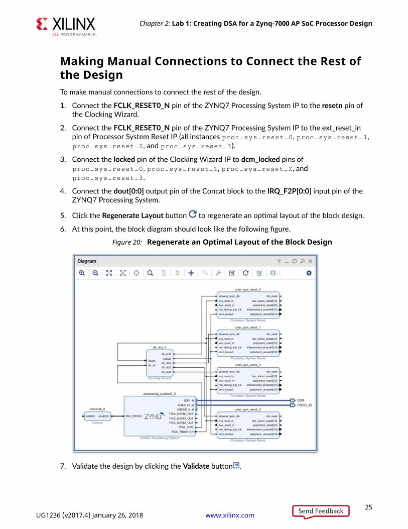
Making Manual Connections to Connect the Rest ofthe DesignTo make manual connections to connect the rest of the design.
1. Connect the FCLK_RESET0_N pin of the ZYNQ7 Processing System IP to the resetn pin ofthe Clocking Wizard.
2. Connect the FCLK_RESET0_N pin of the ZYNQ7 Processing System IP to the ext_reset_inpin of Processor System Reset IP (all instances proc_sys_reset_0, proc_sys_reset_1,proc_sys_reset_2, and proc_sys_reset_3).
3. Connect the locked pin of the Clocking Wizard IP to dcm_locked pins ofproc_sys_reset_0, proc_sys_reset_1, proc_sys_reset_2, andproc_sys_reset_3.
4. Connect the dout[0:0] output pin of the Concat block to the IRQ_F2P[0:0] input pin of theZYNQ7 Processing System.
5. Click the Regenerate Layout button to regenerate an optimal layout of the block design.
6. At this point, the block diagram should look like the following figure.
Figure 20: Regenerate an Optimal Layout of the Block Design
7. Validate the design by clicking the Validate button .
Chapter 2: Lab 1: Creating DSA for a Zynq-7000 AP SoC Processor Design
25UG1236 (v2017.4) January 26, 2018 www.xilinx.com [placeholder text]Send Feedback

8. The Validate Design dialog box pops up. Click OK.
9. Save the block design by clicking the button in the toolbar or by pressing Ctrl+S.
Step 3: Setting Platform PropertiesAfter you complete the hardware platform design project in the Vivado Design Suite, you mustadd platform properties (PFM) to define the platform name and configure platform interfacessuch as clocks, interrupts, and bus interfaces. These properties are set once and stored in theproject.
Platforms typically consists of multiple clocks. In this custom board, our design contains fourdifferent clocks that are produced using a Clocking Wizard. While only one of the clocks out ofthe four is enabled in this lab, you can choose the desired clock frequency in SDx IDE for thehardware functions to be accelerated. Likewise, AXI Ports to be used also need to be identifiedand tagged with the Platform properties so the hardware functions can use these ports to movedata to and from the hardware functions. While these AXI ports may or may not be visible in theblock design used for creating the hardware design in IP integrator, tagging these ports withplatform properties, makes them available for use by the hardware functions later using SDx IDE.
1. The Platform Identification property (PFM_NAME) must be set in the hardware design todefine the Vendor, Library, Name, and Version (VLNV) of the platform. In the Tcl Console,type the following and press Enter. This sets the hardware platform name.
set_property PFM_NAME "xilinx.com:zynq7_board:zynq7_board:1.0"\[get_files [get_property FILE_NAME [get_bd_designs]]]
The PFM_NAME property needs the following syntax:
<vendor>:<library>:<platform>:<version>
2. You can export any clock source with the platform, but for each clock you must also exportsynchronized reset signals using a Processor System Reset IP block in the platform. ThePFM.CLOCK property can be set on BD cell, external port, or external interface. Accordingly,define clocks by typing the following Tcl commands in the Tcl Console and press Enter.
set_property PFM.CLOCK { \ clk_out1 {id "2" is_default "true" proc_sys_reset "proc_sys_reset_0" } \ clk_out2 {id "1" is_default "false" proc_sys_reset "proc_sys_reset_1" } \ clk_out3 {id "0" is_default "false" proc_sys_reset "proc_sys_reset_2" } \ clk_out4 {id "3" is_default "false" proc_sys_reset "proc_sys_reset_3" } \ } [get_bd_cells /clk_wiz_0]
Chapter 2: Lab 1: Creating DSA for a Zynq-7000 AP SoC Processor Design
26UG1236 (v2017.4) January 26, 2018 www.xilinx.com [placeholder text]Send Feedback

3. Define the AXI ports in the design by typing the following in the TCL console and press Enter.
set_property PFM.AXI_PORT { \ M_AXI_GP0 {memport "M_AXI_GP"} \ M_AXI_GP1 {memport "M_AXI_GP"} \ S_AXI_ACP {memport "S_AXI_ACP" sptag "ACP" memory "processing_system7_0 ACP_DDR_LOWOCM"} \ S_AXI_HP0 {memport "S_AXI_HP" sptag "HP0" memory "processing_system7_0 HP0_DDR_LOWOCM"} \ S_AXI_HP1 {memport "S_AXI_HP" sptag "HP1" memory "processing_system7_0 HP1_DDR_LOWOCM"} \ S_AXI_HP2 {memport "S_AXI_HP" sptag "HP2" memory "processing_system7_0 HP2_DDR_LOWOCM"} \ S_AXI_HP3 {memport "S_AXI_HP" sptag "HP3" memory "processing_system7_0 HP3_DDR_LOWOCM"} \ } [get_bd_cells /processing_system7_0]
4. Interrupts must be connected to IP integrator Concat (xlconcat) blocks that are connected tothe processing system. For Zynq®-7000 family it’s the F2P_irq port. Type the followingcommands on the TCL console and press Enter. set intVar []for {set i 0} {$i < 16} {incr i} { lappend intVar In$i {}}set_property PFM.IRQ $intVar [get_bd_cells /xlconcat_0]
5. These properties can be viewed in the Properties windows by selecting the appropriate cellsin the block design canvas. As an example, when you select the Concat cell in the canvas, youwill see a PFM pull down menu in the Block Properties of the Concat block. When the dropdown menu is expanded you will see the IRQ properties for your platform.
Figure 21: Looking up applied PFM Properties
Chapter 2: Lab 1: Creating DSA for a Zynq-7000 AP SoC Processor Design
27UG1236 (v2017.4) January 26, 2018 www.xilinx.com [placeholder text]Send Feedback

Step 4: Generating HDL Design FilesYou now generate the HDL files for the design.
1. To generate the HDL, right-click the zynq7_board block design in the Sources window andfrom the context menu select Generate Output Products.
2. The Generate Output Product dialog box pops up. Select Synthesis → Global, and clickGenerate.
You can also generate the Output Products by typing the following on the Tcl Console.generate_target all [get_files <path_to_project>/zynq7_board/zynq7_board.srcs/sources_1/bd/zynq7_board/zynq7_board.bd]
3. After output products have been generated, the Generate Output Products dialog box opens.Click OK to dismiss the dialog box.
4. Right-click the zynq7_board block design in the Sources window, and select Create HDLWrapper from the context menu.
The Create HDL Wrapper dialog box opens.
5. The Let Vivado manage wrapper and auto-update is selected by default. Click OK.
Figure 22: Create HDL Warpper dialog box
6. Finally, from the menu select File → Export → Export Hardware.
7. The Export Hardware dialog box opens, as shown in the following figure. Click OK.
Chapter 2: Lab 1: Creating DSA for a Zynq-7000 AP SoC Processor Design
28UG1236 (v2017.4) January 26, 2018 www.xilinx.com [placeholder text]Send Feedback
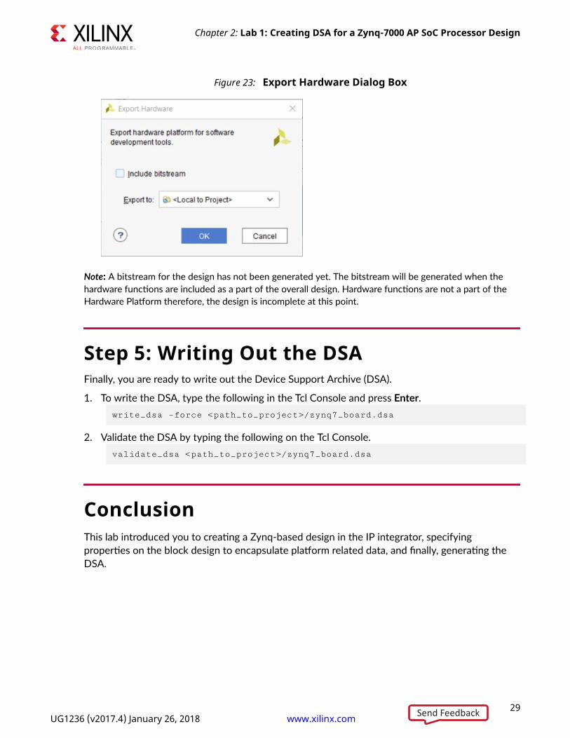
Figure 23: Export Hardware Dialog Box
Note: A bitstream for the design has not been generated yet. The bitstream will be generated when thehardware functions are included as a part of the overall design. Hardware functions are not a part of theHardware Platform therefore, the design is incomplete at this point.
Step 5: Writing Out the DSAFinally, you are ready to write out the Device Support Archive (DSA).
1. To write the DSA, type the following in the Tcl Console and press Enter.write_dsa –force <path_to_project>/zynq7_board.dsa
2. Validate the DSA by typing the following on the Tcl Console.validate_dsa <path_to_project>/zynq7_board.dsa
ConclusionThis lab introduced you to creating a Zynq-based design in the IP integrator, specifyingproperties on the block design to encapsulate platform related data, and finally, generating theDSA.
Chapter 2: Lab 1: Creating DSA for a Zynq-7000 AP SoC Processor Design
29UG1236 (v2017.4) January 26, 2018 www.xilinx.com [placeholder text]Send Feedback

Lab FilesYou can use the Tcl file lab1.tcl that is included with this tutorial design files to perform all thesteps in this lab. To use the Tcl script, launch Vivado and type source lab1.tcl in the Tclconsole.
Alternatively, you can also run the script in the batch mode by typing Vivado -mode batch -source lab1.tcl at the command prompt.
Chapter 2: Lab 1: Creating DSA for a Zynq-7000 AP SoC Processor Design
30UG1236 (v2017.4) January 26, 2018 www.xilinx.com [placeholder text]Send Feedback

Chapter 3
Lab 2: Creating SoftwareComponents for the Platform
In this lab you create software components that are required to create a platform. This processcan be very involved depending on the type of configuration that the platform is being targeted.For example, to create a Linux-based platform you need to use the PetaLinux environment tocreate the required software files. In this lab you create files that are needed for targeting ourplatform to a Standalone or bare-metal system. There are three files needed for targeting aplatform to a Standalone system – First Stage Boot Loader (FSBL), the linker script and the BootImage Format Files (.bif) file.
Step 1: Launching SDKIf you are continuing on from Lab 1, you can launch SDK from Vivado, by selecting File → LaunchSDK. This opens the Launch SDK dialog box.
1. Click OK with default options.
You can also launch SDK from the Start Menu by selecting Xilinx SDK 2017.x. The EclipseLauncher dialog box opens, as shown in the following figure.
Figure 24: Point to the Appropriate Workspace Directory
31UG1236 (v2017.4) January 26, 2018 www.xilinx.com [placeholder text]Send Feedback
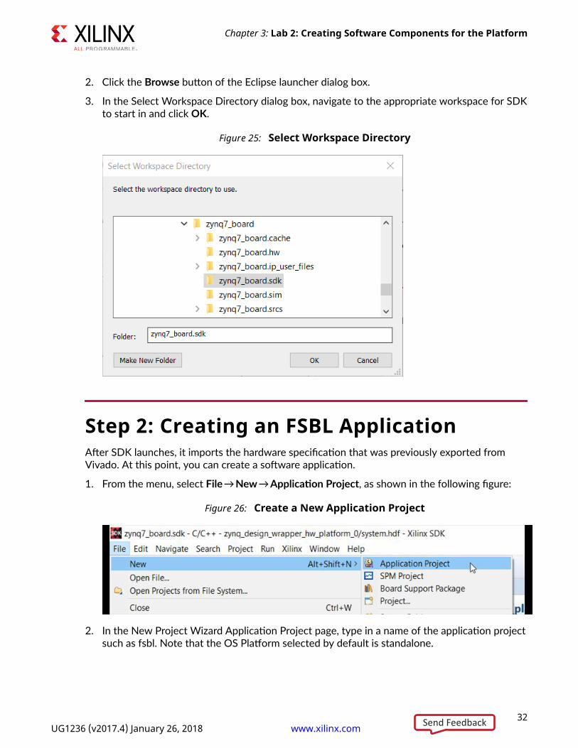
2. Click the Browse button of the Eclipse launcher dialog box.
3. In the Select Workspace Directory dialog box, navigate to the appropriate workspace for SDKto start in and click OK.
Figure 25: Select Workspace Directory
Step 2: Creating an FSBL ApplicationAfter SDK launches, it imports the hardware specification that was previously exported fromVivado. At this point, you can create a software application.
1. From the menu, select File → New → Application Project, as shown in the following figure:
Figure 26: Create a New Application Project
2. In the New Project Wizard Application Project page, type in a name of the application projectsuch as fsbl. Note that the OS Platform selected by default is standalone.
Chapter 3: Lab 2: Creating Software Components for the Platform
32UG1236 (v2017.4) January 26, 2018 www.xilinx.com [placeholder text]Send Feedback
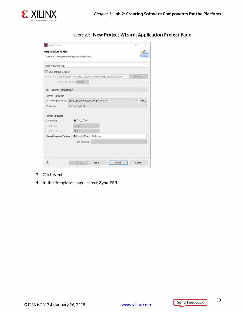
Figure 27: New Project Wizard: Application Project Page
3. Click Next.
4. In the Templates page, select Zynq FSBL.
Chapter 3: Lab 2: Creating Software Components for the Platform
33UG1236 (v2017.4) January 26, 2018 www.xilinx.com [placeholder text]Send Feedback

Figure 28: Select Zynq FSBL Application
5. Click Finish.
6. Ensure that the application has finished compiling by checking the Console.
Figure 29: Ensure that the Application has Finished Compiling
Chapter 3: Lab 2: Creating Software Components for the Platform
34UG1236 (v2017.4) January 26, 2018 www.xilinx.com [placeholder text]Send Feedback
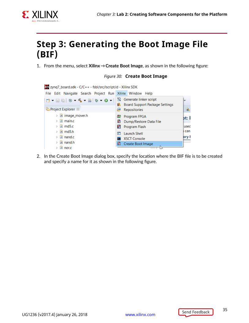
Step 3: Generating the Boot Image File(BIF)1. From the menu, select Xilinx → Create Boot Image, as shown in the following figure:
Figure 30: Create Boot Image
2. In the Create Boot Image dialog box, specify the location where the BIF file is to be createdand specify a name for it as shown in the following figure.
Chapter 3: Lab 2: Creating Software Components for the Platform
35UG1236 (v2017.4) January 26, 2018 www.xilinx.com [placeholder text]Send Feedback
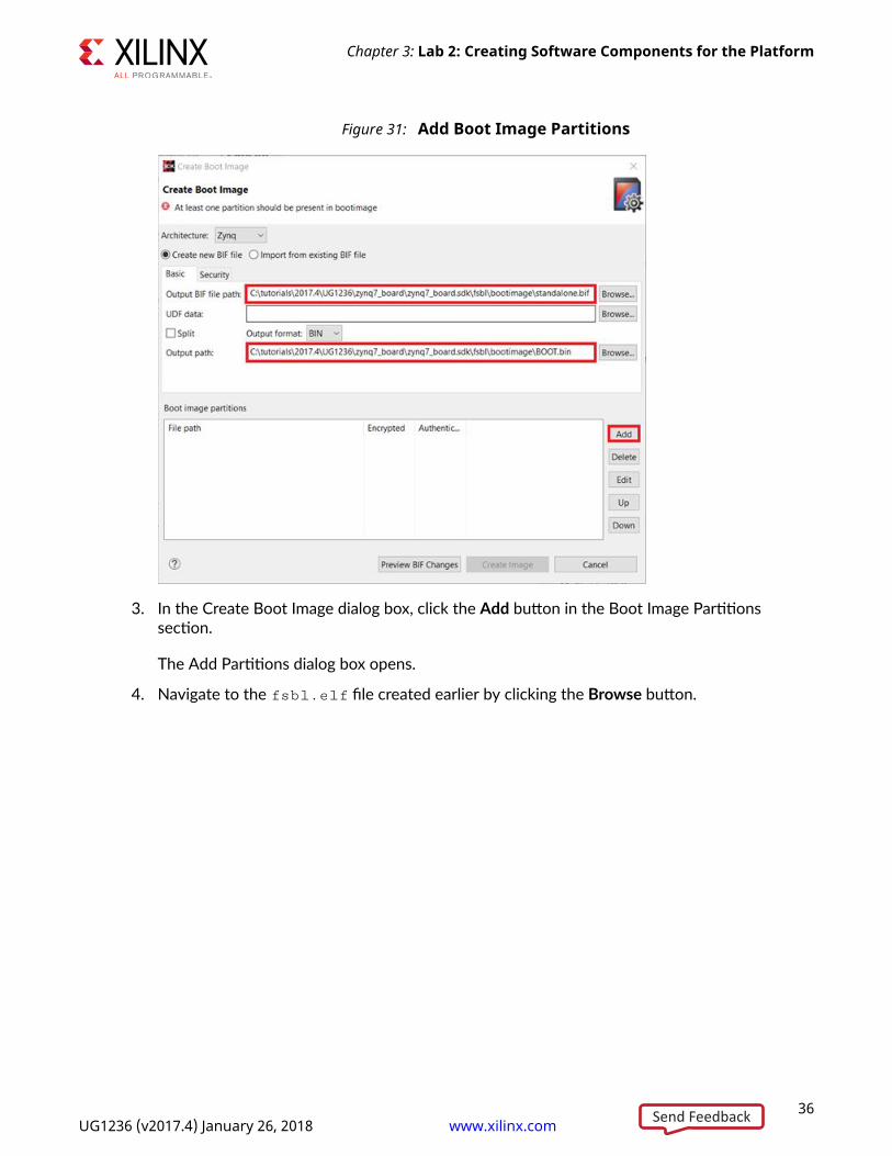
Figure 31: Add Boot Image Partitions
3. In the Create Boot Image dialog box, click the Add button in the Boot Image Partitionssection.
The Add Partitions dialog box opens.
4. Navigate to the fsbl.elf file created earlier by clicking the Browse button.
Chapter 3: Lab 2: Creating Software Components for the Platform
36UG1236 (v2017.4) January 26, 2018 www.xilinx.com [placeholder text]Send Feedback
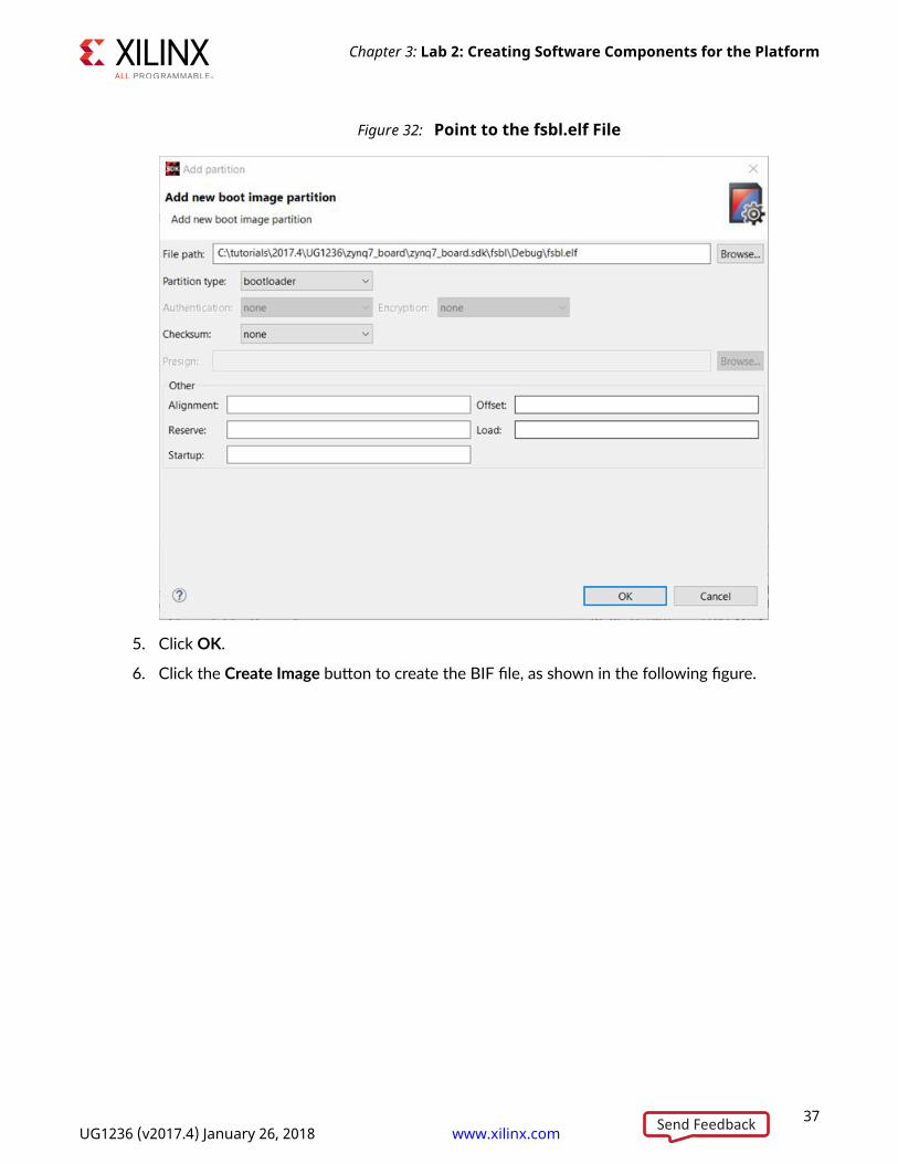
Figure 32: Point to the fsbl.elf File
5. Click OK.
6. Click the Create Image button to create the BIF file, as shown in the following figure.
Chapter 3: Lab 2: Creating Software Components for the Platform
37UG1236 (v2017.4) January 26, 2018 www.xilinx.com [placeholder text]Send Feedback

Figure 33: Create Boot Image
Step 4: Creating a New SoftwareApplication and a Linker ScriptYou need a new linker script to create the Platform in SDx. This linker script ensures that anyapplication code targeted to the custom platform, resides and runs from the DDR memory on theboard. To create a new linker script, you should create an empty application.
1. From the SDK menu, select File → New → Application Project.
2. Specify a name for the project such as empty_application.
Chapter 3: Lab 2: Creating Software Components for the Platform
38UG1236 (v2017.4) January 26, 2018 www.xilinx.com [placeholder text]Send Feedback
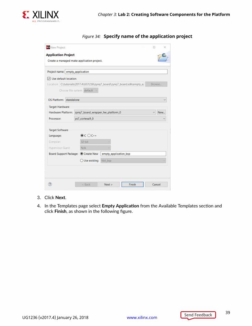
Figure 34: Specify name of the application project
3. Click Next.
4. In the Templates page select Empty Application from the Available Templates section andclick Finish, as shown in the following figure.
Chapter 3: Lab 2: Creating Software Components for the Platform
39UG1236 (v2017.4) January 26, 2018 www.xilinx.com [placeholder text]Send Feedback
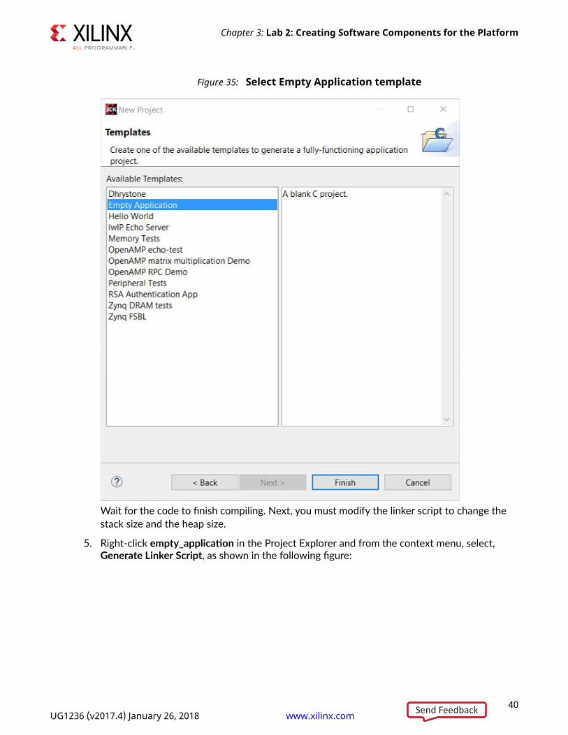
Figure 35: Select Empty Application template
Wait for the code to finish compiling. Next, you must modify the linker script to change thestack size and the heap size.
5. Right-click empty_application in the Project Explorer and from the context menu, select,Generate Linker Script, as shown in the following figure:
Chapter 3: Lab 2: Creating Software Components for the Platform
40UG1236 (v2017.4) January 26, 2018 www.xilinx.com [placeholder text]Send Feedback
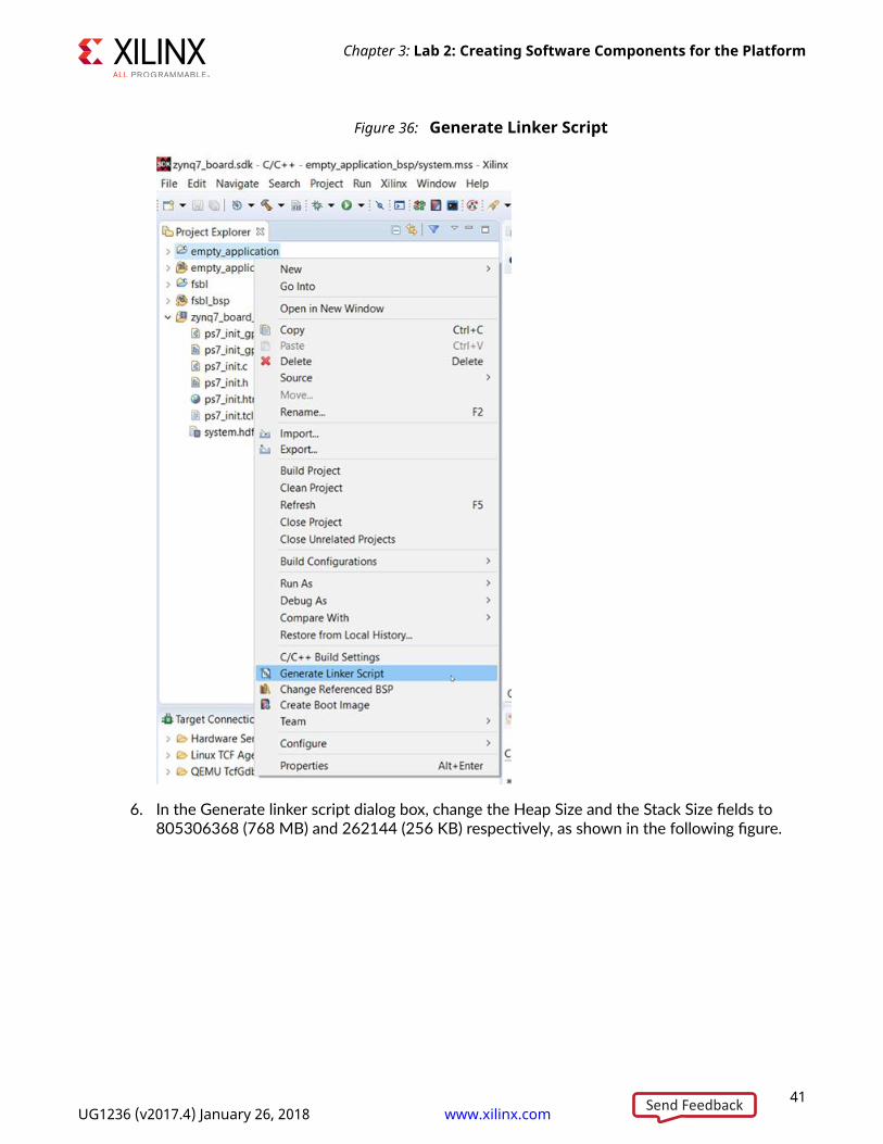
Figure 36: Generate Linker Script
6. In the Generate linker script dialog box, change the Heap Size and the Stack Size fields to805306368 (768 MB) and 262144 (256 KB) respectively, as shown in the following figure.
Chapter 3: Lab 2: Creating Software Components for the Platform
41UG1236 (v2017.4) January 26, 2018 www.xilinx.com [placeholder text]Send Feedback

Figure 37: Change Heap Size and Stack Size
7. With all other values set to default, click Generate.
8. The Linker Script Already Exists! dialog box pops up. Click Yes to overwrite the file.
Figure 38: Overwrite Existing Linker Script
9. Wait for the application to compile with the new linker settings.
10. Exit SDK.
Chapter 3: Lab 2: Creating Software Components for the Platform
42UG1236 (v2017.4) January 26, 2018 www.xilinx.com [placeholder text]Send Feedback
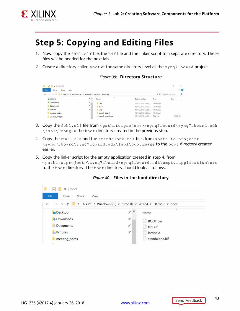
Step 5: Copying and Editing Files1. Now, copy the fsbl.elf file, the bif file and the linker script to a separate directory. These
files will be needed for the next lab.
2. Create a directory called boot at the same directory level as the zynq7_board project.
Figure 39: Directory Structure
3. Copy the fsbl.elf file from <path_to_project>\zynq7_board\zynq7_board.sdk\fsbl\Debug to the boot directory created in the previous step.
4. Copy the BOOT.BIN and the standalone.bif files from <path_to_project>\zynq7_board\zynq7_board.sdk\fsbl\bootimage to the boot directory createdearlier.
5. Copy the linker script for the empty application created in step 4, from<path_to_project>\zynq7_board\zynq7_board.sdk\empty_application\srcto the boot directory. The boot directory should look as follows.
Figure 40: Files in the boot directory
Chapter 3: Lab 2: Creating Software Components for the Platform
43UG1236 (v2017.4) January 26, 2018 www.xilinx.com [placeholder text]Send Feedback
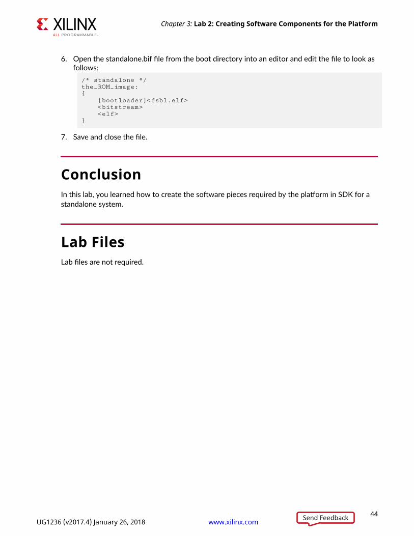
6. Open the standalone.bif file from the boot directory into an editor and edit the file to look asfollows:/* standalone */the_ROM_image:{ [bootloader]<fsbl.elf> <bitstream> <elf>}
7. Save and close the file.
ConclusionIn this lab, you learned how to create the software pieces required by the platform in SDK for astandalone system.
Lab FilesLab files are not required.
Chapter 3: Lab 2: Creating Software Components for the Platform
44UG1236 (v2017.4) January 26, 2018 www.xilinx.com [placeholder text]Send Feedback
Chapter 4
Lab 3: Creating a Custom PlatformUsing the SDx IDE
In this tutorial, you use the SDx IDE to create a custom platform that you have created the DSAfor in Lab 1 and the software components for the standalone configuration in Lab 2. After thecustom platform is created, you add this platform to the available platforms in SDx and targetsoftware applications to the platform.
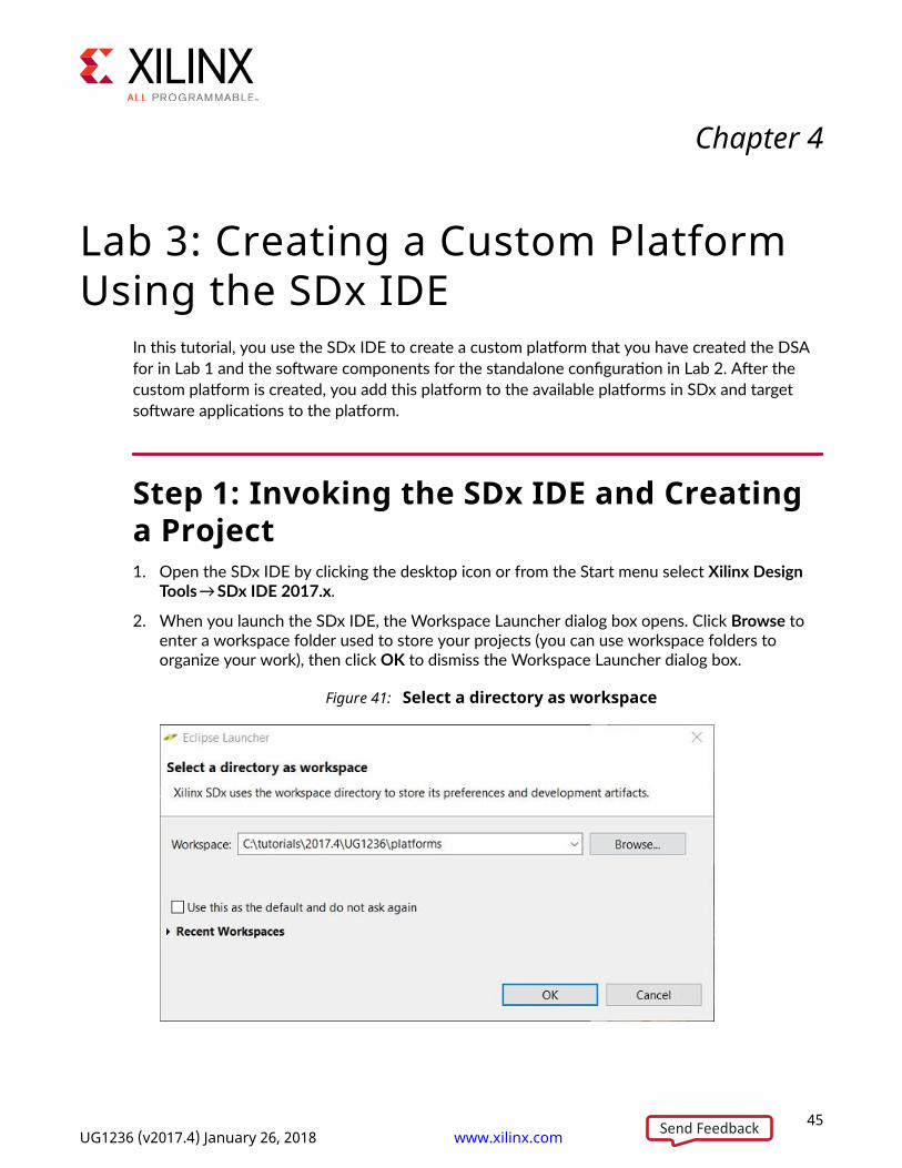
Step 1: Invoking the SDx IDE and Creatinga Project1. Open the SDx IDE by clicking the desktop icon or from the Start menu select Xilinx Design
Tools → SDx IDE 2017.x.
2. When you launch the SDx IDE, the Workspace Launcher dialog box opens. Click Browse toenter a workspace folder used to store your projects (you can use workspace folders toorganize your work), then click OK to dismiss the Workspace Launcher dialog box.
Figure 41: Select a directory as workspace
45UG1236 (v2017.4) January 26, 2018 www.xilinx.com [placeholder text]Send Feedback
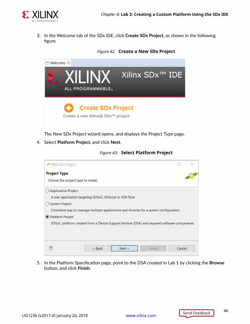
3. In the Welcome tab of the SDx IDE, click Create SDx Project, as shown in the followingfigure.
Figure 42: Create a New SDx Project
The New SDx Project wizard opens, and displays the Project Type page.
4. Select Platform Project, and click Next.
Figure 43: Select Platform Project
5. In the Platform Specification page, point to the DSA created in Lab 1 by clicking the Browsebutton, and click Finish.
Chapter 4: Lab 3: Creating a Custom Platform Using the SDx IDE
46UG1236 (v2017.4) January 26, 2018 www.xilinx.com [placeholder text]Send Feedback
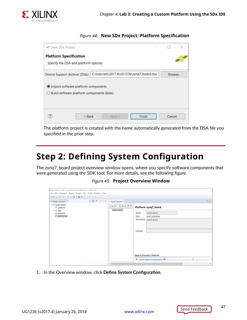
Figure 44: New SDx Project: Platform Specification
The platform project is created with the name automatically generated from the DSA file youspecified in the prior step.
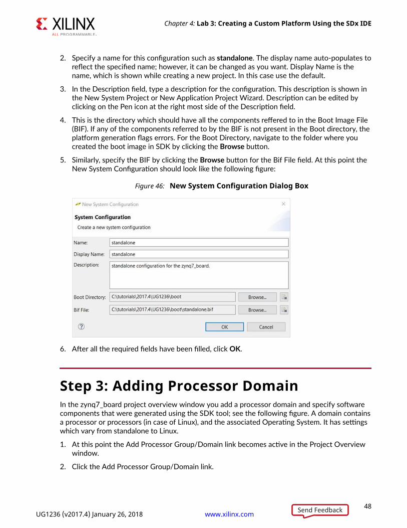
Step 2: Defining System ConfigurationThe zynq7_board project overview window opens, where you specify software components thatwere generated using the SDK tool. For more details, see the following figure.
Figure 45: Project Overview Window
1. In the Overview window, click Define System Configuration.
Chapter 4: Lab 3: Creating a Custom Platform Using the SDx IDE
47UG1236 (v2017.4) January 26, 2018 www.xilinx.com [placeholder text]Send Feedback
2. Specify a name for this configuration such as standalone. The display name auto-populates toreflect the specified name; however, it can be changed as you want. Display Name is thename, which is shown while creating a new project. In this case use the default.
3. In the Description field, type a description for the configuration. This description is shown inthe New System Project or New Application Project Wizard. Description can be edited byclicking on the Pen icon at the right most side of the Description field.
4. This is the directory which should have all the components reffered to in the Boot Image File(BIF). If any of the components referred to by the BIF is not present in the Boot directory, theplatform generation flags errors. For the Boot Directory, navigate to the folder where youcreated the boot image in SDK by clicking the Browse button.
5. Similarly, specify the BIF by clicking the Browse button for the Bif File field. At this point theNew System Configuration should look like the following figure:
Figure 46: New System Configuration Dialog Box
6. After all the required fields have been filled, click OK.
Step 3: Adding Processor DomainIn the zynq7_board project overview window you add a processor domain and specify softwarecomponents that were generated using the SDK tool; see the following figure. A domain containsa processor or processors (in case of Linux), and the associated Operating System. It has settingswhich vary from standalone to Linux.
1. At this point the Add Processor Group/Domain link becomes active in the Project Overviewwindow.
2. Click the Add Processor Group/Domain link.
Chapter 4: Lab 3: Creating a Custom Platform Using the SDx IDE
48UG1236 (v2017.4) January 26, 2018 www.xilinx.com [placeholder text]Send Feedback
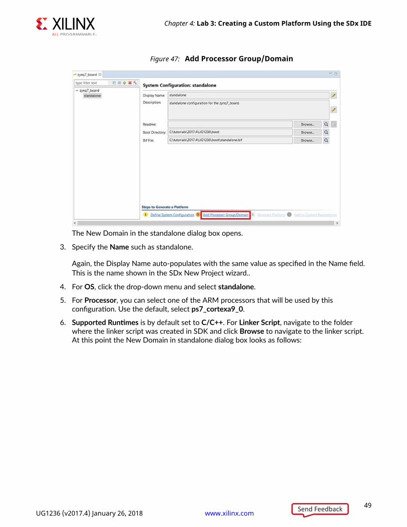
Figure 47: Add Processor Group/Domain
The New Domain in the standalone dialog box opens.
3. Specify the Name such as standalone.
Again, the Display Name auto-populates with the same value as specified in the Name field.This is the name shown in the SDx New Project wizard..
4. For OS, click the drop-down menu and select standalone.
5. For Processor, you can select one of the ARM processors that will be used by thisconfiguration. Use the default, select ps7_cortexa9_0.
6. Supported Runtimes is by default set to C/C++. For Linker Script, navigate to the folderwhere the linker script was created in SDK and click Browse to navigate to the linker script.At this point the New Domain in standalone dialog box looks as follows:
Chapter 4: Lab 3: Creating a Custom Platform Using the SDx IDE
49UG1236 (v2017.4) January 26, 2018 www.xilinx.com [placeholder text]Send Feedback
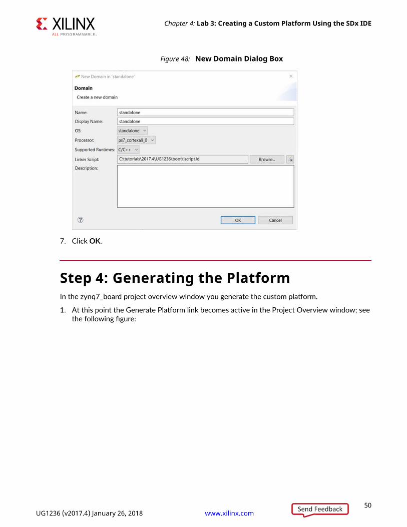
Figure 48: New Domain Dialog Box
7. Click OK.
Step 4: Generating the PlatformIn the zynq7_board project overview window you generate the custom platform.
1. At this point the Generate Platform link becomes active in the Project Overview window; seethe following figure:
Chapter 4: Lab 3: Creating a Custom Platform Using the SDx IDE
50UG1236 (v2017.4) January 26, 2018 www.xilinx.com [placeholder text]Send Feedback

Figure 49: Generate Platform Link in Project Overview Window
2. Click the Generate Platform link.
The Generation completed dialog box opens.
3. Click OK to dismiss the dialog box.
Step 5: Adding Custom Platform toRepositoryIn the zynq7_board project overview window, you add the custom platform to a platformrepository; see the following figure.
1. At this point, the Add to Custom Repositories link becomes active in the Project Overviewwindow.
Chapter 4: Lab 3: Creating a Custom Platform Using the SDx IDE
51UG1236 (v2017.4) January 26, 2018 www.xilinx.com [placeholder text]Send Feedback
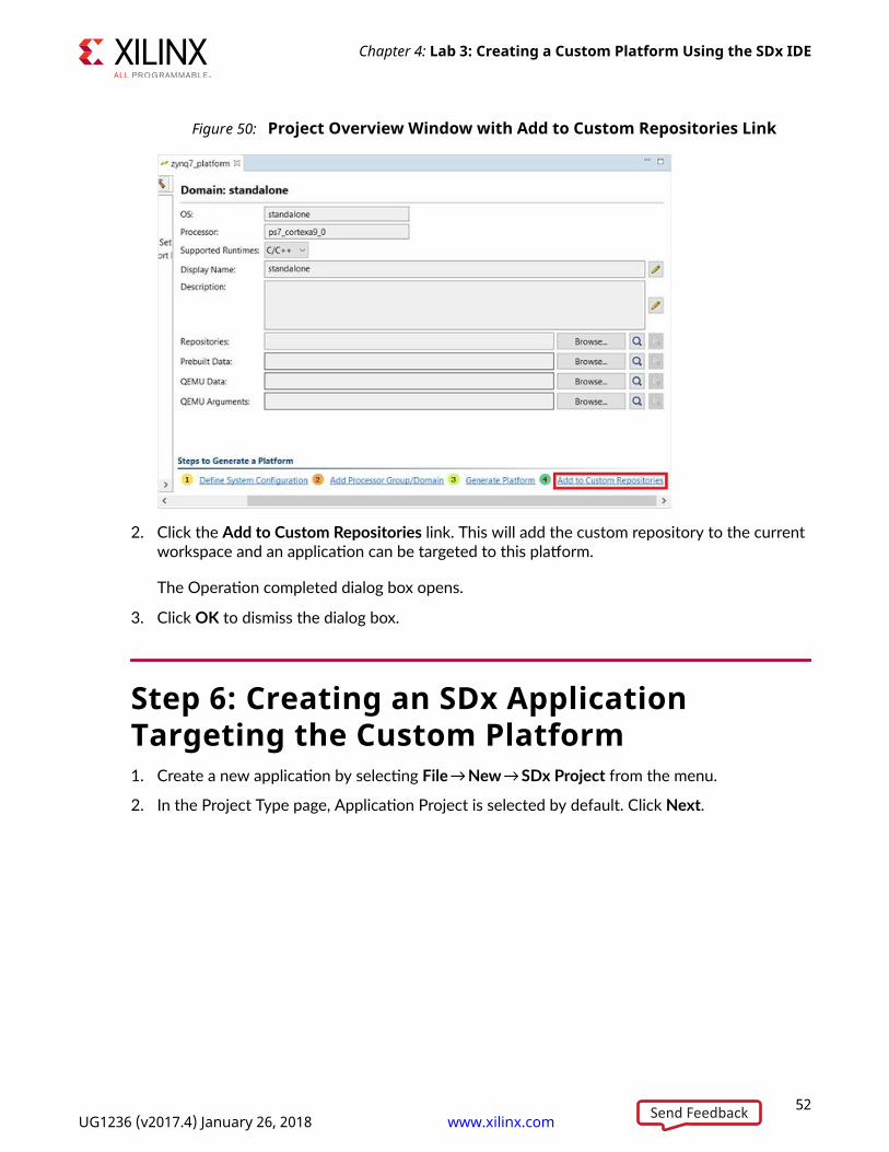
Figure 50: Project Overview Window with Add to Custom Repositories Link
2. Click the Add to Custom Repositories link. This will add the custom repository to the currentworkspace and an application can be targeted to this platform.
The Operation completed dialog box opens.
3. Click OK to dismiss the dialog box.
Step 6: Creating an SDx ApplicationTargeting the Custom Platform1. Create a new application by selecting File → New → SDx Project from the menu.
2. In the Project Type page, Application Project is selected by default. Click Next.
Chapter 4: Lab 3: Creating a Custom Platform Using the SDx IDE
52UG1236 (v2017.4) January 26, 2018 www.xilinx.com [placeholder text]Send Feedback
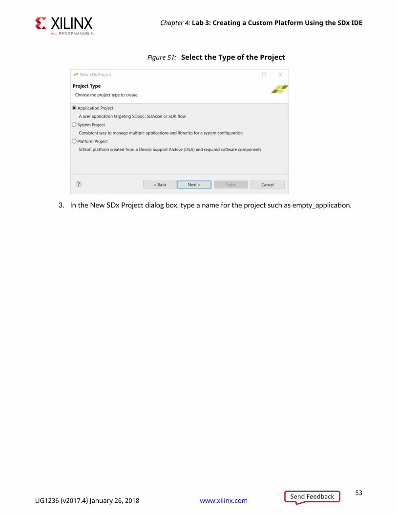
Figure 51: Select the Type of the Project
3. In the New SDx Project dialog box, type a name for the project such as empty_application.
Chapter 4: Lab 3: Creating a Custom Platform Using the SDx IDE
53UG1236 (v2017.4) January 26, 2018 www.xilinx.com [placeholder text]Send Feedback
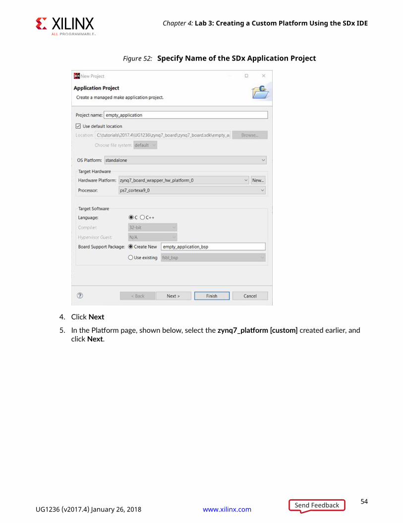
Figure 52: Specify Name of the SDx Application Project
4. Click Next
5. In the Platform page, shown below, select the zynq7_platform [custom] created earlier, andclick Next.
Chapter 4: Lab 3: Creating a Custom Platform Using the SDx IDE
54UG1236 (v2017.4) January 26, 2018 www.xilinx.com [placeholder text]Send Feedback
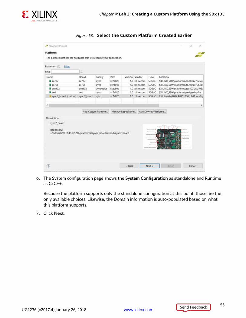
Figure 53: Select the Custom Platform Created Earlier
6. The System configuration page shows the System Configuration as standalone and Runtimeas C/C++.
Because the platform supports only the standalone configuration at this point, those are theonly available choices. Likewise, the Domain information is auto-populated based on whatthis platform supports.
7. Click Next.
Chapter 4: Lab 3: Creating a Custom Platform Using the SDx IDE
55UG1236 (v2017.4) January 26, 2018 www.xilinx.com [placeholder text]Send Feedback
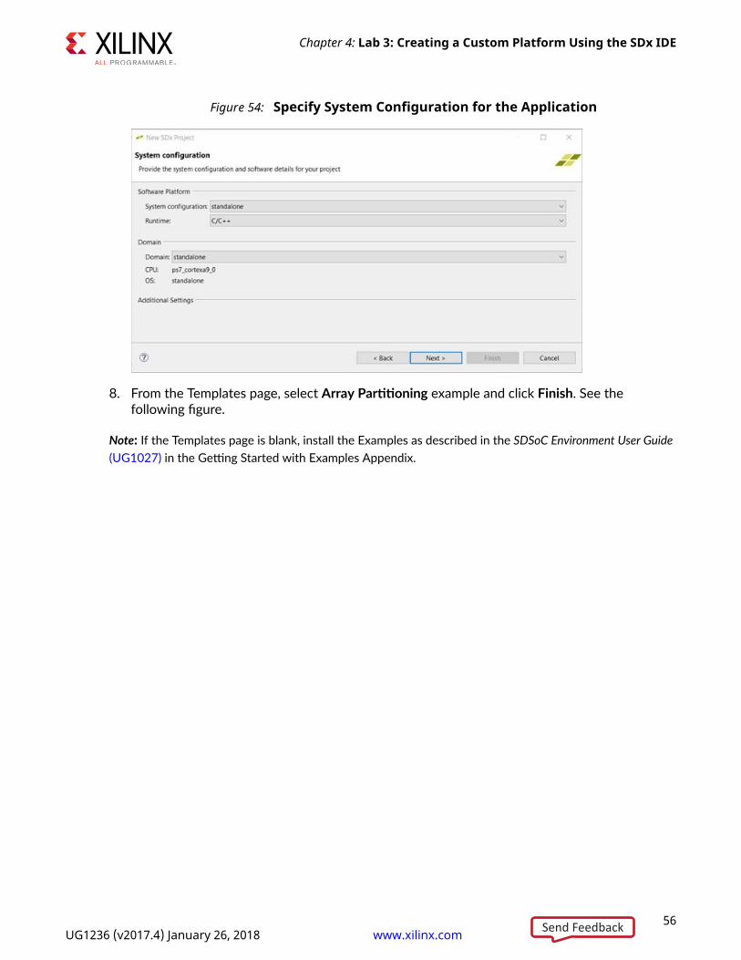
Figure 54: Specify System Configuration for the Application
8. From the Templates page, select Array Partitioning example and click Finish. See thefollowing figure.
Note: If the Templates page is blank, install the Examples as described in the SDSoC Environment User Guide (UG1027) in the Getting Started with Examples Appendix.
Chapter 4: Lab 3: Creating a Custom Platform Using the SDx IDE
56UG1236 (v2017.4) January 26, 2018 www.xilinx.com [placeholder text]Send Feedback
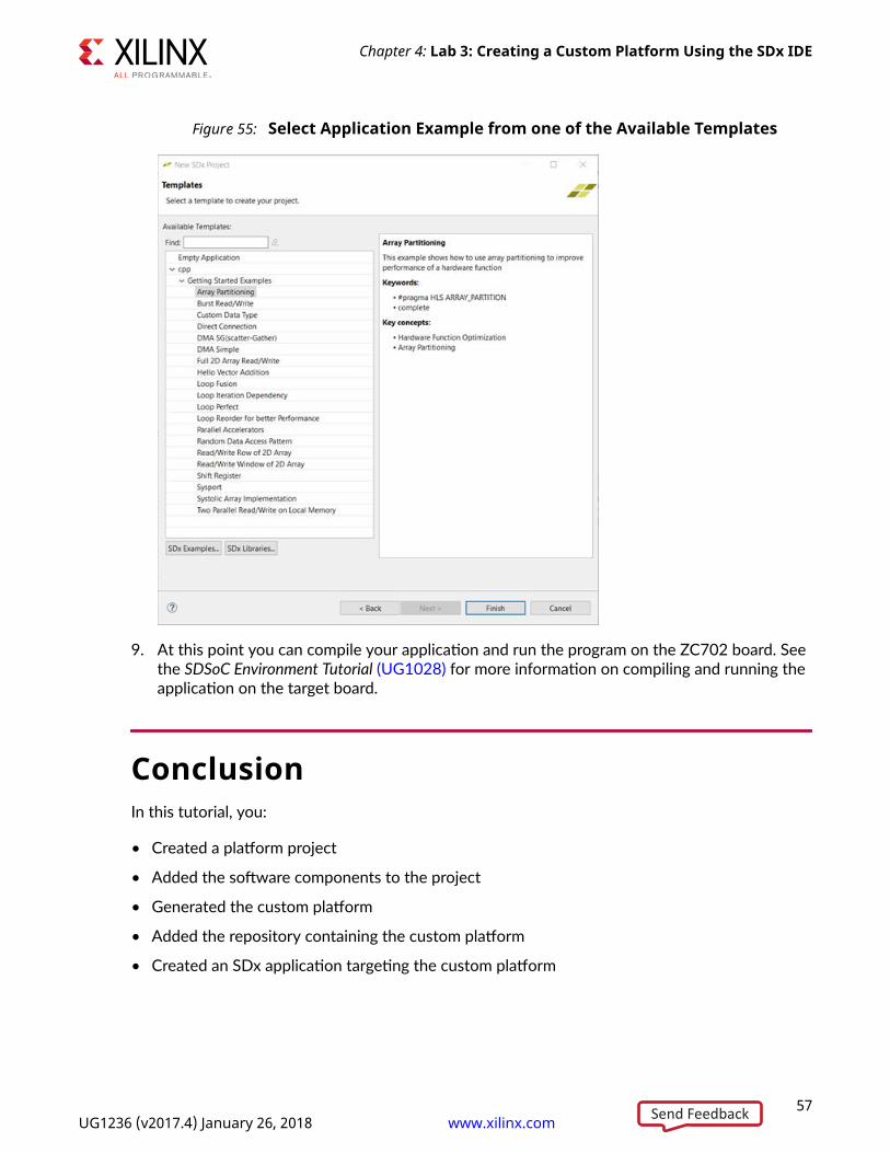
Figure 55: Select Application Example from one of the Available Templates
9. At this point you can compile your application and run the program on the ZC702 board. Seethe SDSoC Environment Tutorial (UG1028) for more information on compiling and running theapplication on the target board.
ConclusionIn this tutorial, you:
• Created a platform project
• Added the software components to the project
• Generated the custom platform
• Added the repository containing the custom platform
• Created an SDx application targeting the custom platform
Chapter 4: Lab 3: Creating a Custom Platform Using the SDx IDE
57UG1236 (v2017.4) January 26, 2018 www.xilinx.com [placeholder text]Send Feedback
Lab FilesLab files are not required.
Chapter 4: Lab 3: Creating a Custom Platform Using the SDx IDE
58UG1236 (v2017.4) January 26, 2018 www.xilinx.com [placeholder text]Send Feedback
Appendix A
Additional Resources and LegalNotices
Xilinx Resources
For support resources such as Answers, Documentation, Downloads, and Forums, see XilinxSupport.
Solution Centers
See the Xilinx Solution Centers for support on devices, software tools, and intellectual propertyat all stages of the design cycle. Topics include design assistance, advisories, and troubleshootingtips
ReferencesThese documents provide supplemental material useful with this webhelp:
1. SDx Environments Release Notes, Installation, and Licensing Guide (UG1238)
2. SDSoC Environment User Guide (UG1027)
3. SDSoC Environment Optimization Guide (UG1235)
4. SDSoC Environment Tutorial: Introduction (UG1028)
5. SDSoC Environment Platform Development Guide (UG1146)
6. SDSoC Development Environment web page
7. UltraFast Embedded Design Methodology Guide (UG1046)
8. Zynq-7000 All Programmable SoC Software Developers Guide (UG821)
9. Zynq UltraScale+ MPSoC Software Developer Guide (UG1137)
10. ZC702 Evaluation Board for the Zynq-7000 XC7Z020 All Programmable SoC User Guide (UG850)
11. ZCU102 Evaluation Board User Guide (UG1182)
12. PetaLinux Tools Documentation: Workflow Tutorial (UG1156)
13. Vivado Design Suite User Guide: High-Level Synthesis (UG902)
59UG1236 (v2017.4) January 26, 2018 www.xilinx.com [placeholder text]Send Feedback
14. Vivado Design Suite User Guide: Creating and Packaging Custom IP (UG1118)
15. Vivado® Design Suite Documentation
Please Read: Important Legal NoticesThe information disclosed to you hereunder (the "Materials") is provided solely for the selectionand use of Xilinx products. To the maximum extent permitted by applicable law: (1) Materials aremade available "AS IS" and with all faults, Xilinx hereby DISCLAIMS ALL WARRANTIES ANDCONDITIONS, EXPRESS, IMPLIED, OR STATUTORY, INCLUDING BUT NOT LIMITED TOWARRANTIES OF MERCHANTABILITY, NON-INFRINGEMENT, OR FITNESS FOR ANYPARTICULAR PURPOSE; and (2) Xilinx shall not be liable (whether in contract or tort, includingnegligence, or under any other theory of liability) for any loss or damage of any kind or naturerelated to, arising under, or in connection with, the Materials (including your use of theMaterials), including for any direct, indirect, special, incidental, or consequential loss or damage(including loss of data, profits, goodwill, or any type of loss or damage suffered as a result of anyaction brought by a third party) even if such damage or loss was reasonably foreseeable or Xilinxhad been advised of the possibility of the same. Xilinx assumes no obligation to correct anyerrors contained in the Materials or to notify you of updates to the Materials or to productspecifications. You may not reproduce, modify, distribute, or publicly display the Materialswithout prior written consent. Certain products are subject to the terms and conditions ofXilinx's limited warranty, please refer to Xilinx's Terms of Sale which can be viewed at https://www.xilinx.com/legal.htm#tos; IP cores may be subject to warranty and support terms containedin a license issued to you by Xilinx. Xilinx products are not designed or intended to be fail-safe orfor use in any application requiring fail-safe performance; you assume sole risk and liability foruse of Xilinx products in such critical applications, please refer to Xilinx's Terms of Sale which canbe viewed at https://www.xilinx.com/legal.htm#tos.
AUTOMOTIVE APPLICATIONS DISCLAIMER
AUTOMOTIVE PRODUCTS (IDENTIFIED AS "XA" IN THE PART NUMBER) ARE NOTWARRANTED FOR USE IN THE DEPLOYMENT OF AIRBAGS OR FOR USE IN APPLICATIONSTHAT AFFECT CONTROL OF A VEHICLE ("SAFETY APPLICATION") UNLESS THERE IS ASAFETY CONCEPT OR REDUNDANCY FEATURE CONSISTENT WITH THE ISO 26262AUTOMOTIVE SAFETY STANDARD ("SAFETY DESIGN"). CUSTOMER SHALL, PRIOR TO USINGOR DISTRIBUTING ANY SYSTEMS THAT INCORPORATE PRODUCTS, THOROUGHLY TESTSUCH SYSTEMS FOR SAFETY PURPOSES. USE OF PRODUCTS IN A SAFETY APPLICATIONWITHOUT A SAFETY DESIGN IS FULLY AT THE RISK OF CUSTOMER, SUBJECT ONLY TOAPPLICABLE LAWS AND REGULATIONS GOVERNING LIMITATIONS ON PRODUCTLIABILITY.
Appendix A: Additional Resources and Legal Notices
60UG1236 (v2017.4) January 26, 2018 www.xilinx.com [placeholder text]Send Feedback
Copyright
© Copyright 2017-2018 Xilinx®, Inc. Xilinx®, the Xilinx® logo, Artix, ISE, Kintex, Spartan,Virtex, Vivado, Zynq, and other designated brands included herein are trademarks of Xilinx in theUnited States and other countries.OpenCL and the OpenCL logo are trademarks of Apple Inc.used by permission by Khronos.All other trademarks are the property of their respective owners.
Appendix A: Additional Resources and Legal Notices
61UG1236 (v2017.4) January 26, 2018 www.xilinx.com [placeholder text]Send Feedback

Appendix A: Additional Resources and Legal Notices
62UG1236 (v2017.4) January 26, 2018 www.xilinx.com [placeholder text]Send Feedback