Embed Size (px)
Citation preview

7/27/2019 UEEA1253_LAB2
http://slidepdf.com/reader/full/ueea1253lab2 1/15
UEEA1253 – CIRCUITS, SIGNALS
AND SYSTEMS
LAB 2
NAME : RAJALAKSHMI NADARAJAN / HEMALATHA GANESAN
ID : 09UEB05159 / 09UEB07309
COURSE : EC/ MH
DATE OF EXPERIMENT : 28 MARCH 2012
CONTACT : 017-3608012 / 014-3258728
EMAIL : [email protected] / [email protected]
1

7/27/2019 UEEA1253_LAB2
http://slidepdf.com/reader/full/ueea1253lab2 2/15
R g
~
R Lv
g
Signal Generator
v L
Introduction:
Impedance matching is a technique of impedance transformation so that the maximum
power transfer can be possible. Passive LC networks are used to match impedances
between the source (generator) and a load. These matching networks are designed
usingcombinations of inductors and capacitors.
Objectives:
a) To measure the power transfer coefficient of a circuit.
b) To show how impedance matching can improve the power transfer to the load for a
narrowband about the frequency of interest.
c) To understand theory and advantages of impedance matching.
Theory:
Maximum Power Transfer is used to ensuring the maximum amount of power that
going to dissipated in the load resistance, RL when value of the load resistance is
exactly equal to the resistance of the power source, Rg. The load impedance and the
internal impedance of the energy source have a relationship among themselves; the
different load impedance will give different value of power in the load.
The maximum power transfer can be seen by using a Thevenin equivalent circuit.
Generally, maximum power transfer theorem states that "the maximum amount of
power will be dissipated in the load resistance if it is equal in value to the Thevenin
or Norton source resistance of the network supplying the power ". Which mean when
, we can get the maximum power transfer for the circuit.
Impedance matching is a design to maximize the power transfer and minimize the
reflection of its corresponding signal source from the load by changing the input
impedance of an electrical load or in other word output impedance. Generally,
impedance matching is a design that making the load resistance, to get near to
internal resistance so that the maximum among of power can be dissipated in the
load resistance
2

7/27/2019 UEEA1253_LAB2
http://slidepdf.com/reader/full/ueea1253lab2 3/15
We going to do experiment on an LC circuit as an impedance transformer so that the
load resistor appears as R g to improve the power transfer ratio at an operating
frequency. By analyzing the Z(f) above, get its real part R(f) and imaginary part X(f)
in terms of L, C and R L .
R s = R LThe equation that can be derived is as shown below
Equipments and components:
• Signal generator and oscilloscope
• One each (10, 33, 56, 68, 100, 220, 330, 470 and 680 Ω) resistors, one 10mH
inductor and three 100nF capasitor
• Resistance box, Inductor box and Capacitor box.
3
Vs
I
R L
R s

7/27/2019 UEEA1253_LAB2
http://slidepdf.com/reader/full/ueea1253lab2 4/15
R g
~
R Lv
g
Signal Generator
v L
Method:
Experiment 1: Measurement of the power transfer coefficient
NOTE: All the voltage measurement was done using the oscilloscope
a.)The sine wave f = 3kHz and v s = 16V pp(oscilloscope). Vs(peak value) = 8V p. The
calculated .
b) The R g value was measured. R g = 42.94 Ω
R L = 100.2
c) The maximum power available:
d) The Lv (rms) was measured for various values of resistor load R L given: 9.9Ω,
32.9Ω, 55.9Ω, 67.9Ω, 100.2Ω, 216.6Ω, 325.2Ω, 461Ω and 670Ω.
e) was calculated.
f) The power transfer coefficient was calculated.
No R L (Ω) VL(RMS)
1 9.9 0.892 0.0804 0.4232
2 32.9 2.157 0.1414 0.7442
3 55.9 2.885 0.1489 0.7837
4 67.9 3.146 0.1458 0.7674
5 100.2 3.640 0.1322 0.6958
6 216.6 5.020 0.1163 0.6121
7 325.2 5.360 0.0883 0.46478 461 5.570 0.0673 0.3542
9 670 5.820 0.0506 0.2663
4

7/27/2019 UEEA1253_LAB2
http://slidepdf.com/reader/full/ueea1253lab2 5/15
NOTE: After calculating if the t >1, the experiment was repeated again as the R g
value was wrongly measured or calculated.
g) The graph t against R L was plotted
Observation:
From the graph the maximum value of the t is 0.7837 when the R L value is equal55.9Ω.
Experiment 2: Impedance Matching for maximum power transfer
When R g is as measured and the load resistor R L = 670 Ω a mismatching occurs. The
calculated power transfer ratio is:
In this experiment an LC circuit was an impedance transformer so that the 670 Ω load
resistor appears as R g to improve the power transfer ratio at an operating frequency.
Assumption made was that a 10mH inductor was provided.
5
7/27/2019 UEEA1253_LAB2
http://slidepdf.com/reader/full/ueea1253lab2 6/15
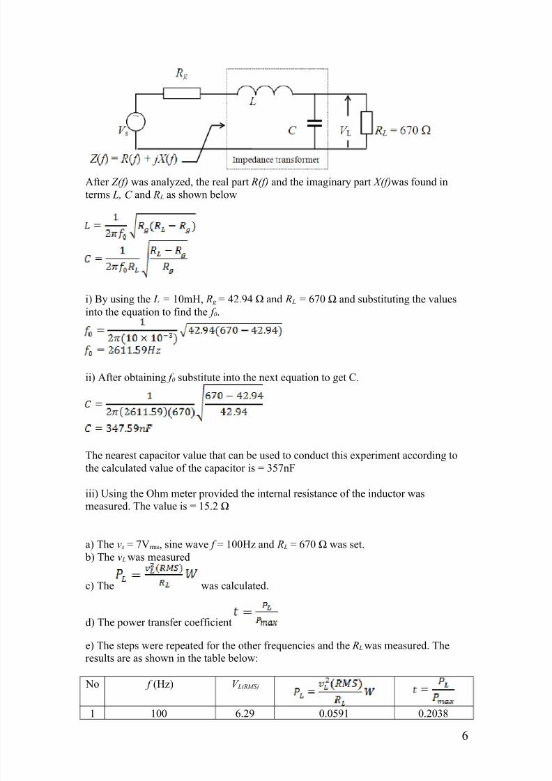
After Z(f) was analyzed, the real part R(f) and the imaginary part X(f)was found in
terms L, C and R L as shown below
i) By using the L = 10mH, R g = 42.94 Ω and R L = 670 Ω and substituting the values
into the equation to find the f 0.
ii) After obtaining f 0 substitute into the next equation to get C.
The nearest capacitor value that can be used to conduct this experiment according to
the calculated value of the capacitor is = 357nF
iii) Using the Ohm meter provided the internal resistance of the inductor was
measured. The value is = 15.2 Ω
a) The v s = 7Vrms, sine wave f = 100Hz and R L = 670 Ω was set. b) The v L was measured
c) The was calculated.
d) The power transfer coefficient
e) The steps were repeated for the other frequencies and the R L was measured. The
results are as shown in the table below:
No f (Hz) V L(RMS)
1 100 6.29 0.0591 0.2038
6

7/27/2019 UEEA1253_LAB2
http://slidepdf.com/reader/full/ueea1253lab2 7/15
2 500 6.52 0.0634 0.2186
3 1000 6.99 0.0729 0.2513
4 2000 9.09 0.1233 0.4252
5 2500 10.30 0.1583 0.5459
6 3000 10.18 0.1547 0.5334
7 3500 7.53 0.0846 0.29178 4000 4.97 0.03686 0.1271
9 5000 2.22 7.3558x10⁻³ 0.0254
10 6000 1.40 2.9254x10⁻³ 0.0101
11 7000 0.976 1.4218x10⁻³ 4.90x10⁻³
12 8000 0.718 7.6944x10⁻⁴ 2.65x10⁻³
g) The graph t against f was plotted
Observation:
From the graph the maximum value of t is 0.5459 when the frequency is 2500Hz.
When the frequency is increasing, we can see that the power transfer coefficient ,t is
increasing until one point which is the peak of the curve, the power transfer
coefficient , t decreasing after that point .
Discussion:
In the first experiment,the value of t isnot more than 1.Therefore the value of R gobtained is correct.Based on the graph it can be seen that the value of t is increasing
for the value of R L 9.9Ω to 55.9Ω. Then as the value of R L increases from 67.9Ω to
670Ω the value t is decreasing gradually. From the table we can say that the VL(RMS)
increases as the R L value increases. The PL value also shows the same characteristic asthe t value that is when the R L value is 9.9Ω to 55.9Ω it is increasing and as the R L
value increases from 67.9Ω to 670Ω it decreases.
7

7/27/2019 UEEA1253_LAB2
http://slidepdf.com/reader/full/ueea1253lab2 8/15
R g
~
R Lv
g
Signal Generator
v L
For the second experiment from the table itself it can be seen and concluded that the
value of t , VL(RMS) and the PL value is increasing for the value of the frequency starting
from 100Hz to 2500Hz. All the three values starts to decrease when the frequency is
increasing from 3000Hz to 8000Hz
After each experiment, the power transfer coefficient, t is calculated.It should not bemore than 1 for both experiments.This is because the power that transfers will not
bigger than the maximum power available. If the coefficient, t is bigger than 1, it
simply means the circuit is generating or amplifying the power from the input.
Unfortunately, in the experiment 3.1 and experiment 3.2, the circuit that we connected
is not one of an amplifying type. Hence, the power transfer coefficient, t will be 1 and
will not more then 1. Or in other word, the power transfer coefficient, t is showing the
remaining power after the power loss from the input power.
There are few precautionary steps we need to check. First, all the apparatus should be
tested to make sure there was not any apparatus was not functioning or functioning in
a good condition. Besides that, the materials that we use such as resistors, capacitors
and also the inductors are needed to be checked. This may save up time in doing theexperiment so that we will not keep getting the wrong result and force to redo the
experiment as we do not know the apparatus and material that we used is not
functioning.
The position of the eyes must be correct when reading the scale.This is to avoid
parallax error.In both experiments we need to measure the VL ,if the value were
measured wrongly it will effect the whole experiment results.
Analysis and Confirmation of Experimental Results:
Experiment 1: Measurement of the power transfer coefficient
By using the equation we can obtain the theoretical values for the
experiment 1.
8

7/27/2019 UEEA1253_LAB2
http://slidepdf.com/reader/full/ueea1253lab2 9/15
No R L (Ω) VL(RMS)
1 10 1.0691 0.1143 0.6016
2 33 2.4596 0.1833 0.9648
3 56 3.2036 0.1833 0.9645
4 68 3.4693 0.1770 0.9316
5 100 3.9597 0.1568 0.8252
6 220 4.7357 0.1019 0.5365
7 330 5.0083 0.0760 0.4000
8 470 5.1862 0.0572 0.3012
9 680 5.3238 0.0417 0.2194
The graph t against R L was plotted.
Observation:From the graph the maximum value of the t is 0.9648 when the R L value is equal
33Ω.When we compare the theoretical and the experimental graph,it is almost the
same.Even if there is a slight difference it may be because due to the technical
problem exist in the experimental tools used.
Experiment 2: Impedance Matching for maximum power transfer
For this experiment we analyze it in two which in the first case where it is an ideal
inductor and the second case inductance with the internal resistance.
Case 1: Ideal inductor
9

7/27/2019 UEEA1253_LAB2
http://slidepdf.com/reader/full/ueea1253lab2 10/15
---------- 1
-------- 2
-------- 3
-------- 4
By substituting equation 2 into 1 we obtain:
By substituting 2 into 3 we obtain:
By substituting 1 into 4 we obtain:
In terms of
Substituting into the equation we obtain:
By solving we obtain:
10

7/27/2019 UEEA1253_LAB2
http://slidepdf.com/reader/full/ueea1253lab2 11/15
By using the values below and substituting into the equation above we ob tain the
results as shown in the table below:
No f (Hz) V L(RMS)
1 100 628.31854 5.66 0.047 0.230
2 500 3141.5927 6.36 0.059 0.289
3 1000 6283.1854 7.07 0.074 0.363
4 2000 12566.370
8
8.49 0.106 0.520
5 2500 15707.963
5
9.55 0.134 0.657
6 3000 18849.556
2
10.61 0.166 0.814
7 3500 21991.148
9
9.55 0.134 0.657
8 4000 25132.741
6
7.07 0.074 0.363
9 5000 31415.927 3.54 0.018 0.088
10 6000 37699.112
4
2.26 0.007 0.034
11 7000 43982.297
8
1.56 0..004 0.020
12 8000 50265.483
2
1.10 0.002 0.009
The graph t against f was plotted.
11

7/27/2019 UEEA1253_LAB2
http://slidepdf.com/reader/full/ueea1253lab2 12/15
Observation:
From the graph the maximum value of t is 0.814 when the frequency is 2000Hz.
Case 2: Inductance with internal resistance of 15.2Ω
----------1
---------- 2
---------- 3
---------- 4
By substituting equation 2 into 1 we obtain:
By substituting 2 into 3 we obtain:
By substituting 1 into 4 we obtain:
12

7/27/2019 UEEA1253_LAB2
http://slidepdf.com/reader/full/ueea1253lab2 13/15
In terms of
Substituting into the equation we obtain:
By solving we obtain:
By using the values below and substituting into the equation above we ob tain the
results as shown in the table below:
No f (Hz) V L(RMS)
1 100 628.31854 4.557 0.031 0.169
2 500 3141.5927 4.634 0.032 0.175
3 1000 6283.1854 4.887 0.035 0.191
4 2000 12566.370
8
6.015 0.053 0.290
5 2500 15707.963
5
6.786 0.068 0.372
6 3000 18849.556
2
7.071 0.074 0.404
7 3500 21991.148
9
6.223 0.057 0.311
8 4000 25132.741
6
4.817 0.034 0.186
13

7/27/2019 UEEA1253_LAB2
http://slidepdf.com/reader/full/ueea1253lab2 14/15
9 5000 31415.927 2.766 0.011 0.060
10 6000 37699.112
4
1.751 0.005 0.027
11 7000 43982.297
8
1.210 0.002 0.011
12 8000 50265.4832
0.890 0.001 0.005
The graph t against f was plotted.
Observation:
From the graph the maximum value of t is 0.404 when the frequency is 3000Hz.
Comment:
Ideal inductor means having no resistance (impedance), is also known as inductance.
In ideal inductor case, the t value found that is slightly more than value t with internal
resistance of inductor. This proved that the impedance matching can improve the load
fornarrowband frequency. By plotting a graph, we can easily know the maximum power transfer.
Conclusion:
Based on the experiment, impedance matching techniques can known the electronics
design practice of setting the input impedance ( Z L) of an electrical load equal to the
fixed output impedance ( Z S) of the signal source to which it is ultimately connected,
usually in order to maximize the power transfer and minimize reflections from the
load. This only applies when both are linear devices
Reference:
John Bird. Revised edition(2003). Electrical Circuit Theory and Technology. Burlington,MA Newnes
14

7/27/2019 UEEA1253_LAB2
http://slidepdf.com/reader/full/ueea1253lab2 15/15
Impedance Matching Basics - Series L and C. (n.d.). Retrieved April 12, 2011, from Antenna-
Theory.com: http://www.antenna-theory.com/tutorial/smith/smithchart5.php
Impedance matching. (2011, April 3). Retrieved April 12, 2011, from Wkipedia:
http://en.wikipedia.org/wiki/Impedance_matching
15


