Embed Size (px)
Citation preview

UCF Senior Design II
Department of Electrical Engineering and Computer Science
University of Central Florida Dr. Lei Wei
Group 2
David Simoneau Computer Engineering
Chris Britt Electrical Engineering
Anthony Hunter Hinnant Computer Engineering
Francisco Tirado Perez Computer Engineering

II
Table of Contents
List of Figures ................................................................................................................... VI
List of Equations ............................................................................................................... IX
List of Tables .................................................................................................................... IX
1: Executive Summary ........................................................................................................ 1
2: Requirement Specifications ............................................................................................ 2
3: House of Quality ............................................................................................................. 5
4: Block Diagrams .............................................................................................................. 7
5: Milestones ..................................................................................................................... 10
6: Cost ............................................................................................................................... 12
7: Project Management ..................................................................................................... 12
Project Management Staff ...................................................................................... 12
Why Projects Fail ................................................................................................... 13
Project Management Goals .................................................................................... 14
Project Management – Team Building .................................................................. 14
8: Glove Design ................................................................................................................ 14
Glove Construction ................................................................................................ 15
Power...................................................................................................................... 15
Heating and Cooling .............................................................................................. 15
Peltier Selection ..................................................................................................... 15
Switching Direction Using N-FETs ....................................................................... 17
Switching Direction Using an H-Bridge ................................................................ 18
Controlling Magnitude with a Digital to Analog Converter .................................. 19
Controlling Magnitude with a Digital Potentiometer ............................................ 20
Digital Potentiometer Part Selection ...................................................................... 22
Operational Amplifier Part Selection ................................................................... 22
Switching FET Circuit and Part Selection ........................................................... 23
Controlling Temperature of the Peltier ................................................................ 24
Thermistor Selection and Implementation ........................................................... 27
Final Peltier Controller with Enable and Phase ................................................... 28
Battery Selection .................................................................................................. 29
8.15.1: Nickel-Metal Hydride .................................................................................... 30
8.15.2: Nickel-Zinc .................................................................................................... 30

III
8.15.3: Lithium Ion .................................................................................................... 31
Battery Choice ...................................................................................................... 31
Charger Selection ................................................................................................. 31
Power Regulators ................................................................................................. 32
8.18.1: Regulator Selection ....................................................................................... 32
8.18.2: Timing Regulator........................................................................................... 34
Housing ................................................................................................................ 35
8.19.1: Light Emitting Diode ..................................................................................... 36
Haptic Feedback ................................................................................................... 36
8.20.1: Linear Resonant Actuators ............................................................................ 37
8.20.2: Eccentric Rotating Mass Vibrational Motors ................................................ 37
8.20.3: Haptic Feedback Part Selection ..................................................................... 38
Motion Tracking................................................................................................... 38
8.21.1: Optical Tracking ............................................................................................ 39
8.21.2: Inertial Sensors .............................................................................................. 39
8.21.3: Accelerometer Considerations ....................................................................... 40
8.21.4: Accelerometer Choice ................................................................................... 40
8.21.5: I2C Multiplexer ............................................................................................. 41
Final Hardware Implementation .......................................................................... 42
9: Processing Board Overview.......................................................................................... 43
Processor Comparisons .......................................................................................... 43
9.1.1: The STM32F030C8T6 .................................................................................... 45
Input and Output through Processor ...................................................................... 46
Wireless Communication ....................................................................................... 48
9.3.1: Pros and Cons of Wireless Communication .................................................... 48
9.3.2: Bluetooth Module Choices .............................................................................. 48
9.3.3: Bluetooth Specifications .................................................................................. 51
PCB Design ............................................................................................................ 51
9.4.1: Schematic Design Tools .................................................................................. 52
9.4.2: KiCAD ............................................................................................................. 52
9.4.3: SOLIDWORKS PCB ...................................................................................... 52
9.4.4: DesignSpark PCB ............................................................................................ 52
PCB Fabrication ..................................................................................................... 53
9.5.1: PCBWay .......................................................................................................... 53

IV
9.5.2: 4pcb ................................................................................................................. 53
9.5.3: PCBgogo.......................................................................................................... 54
9.5.4: JLCPCB ........................................................................................................... 54
PCB Design Constraints ......................................................................................... 54
9.6.1: Environmental Constraints .............................................................................. 54
9.6.2: Economical Constraints ................................................................................... 54
9.6.3: Sustainability Constraints ................................................................................ 55
9.6.4: Social and Political Constraints ....................................................................... 55
9.6.5: Ethical Constraints........................................................................................... 55
9.6.6: Health and Safety Constraints ......................................................................... 55
System Startup Procedure ...................................................................................... 55
10: Relevant Technologies ................................................................................................ 57
Existing Technologies and Products .................................................................... 57
10.1.1: VRGluv.......................................................................................................... 57
10.1.2: HAPTX .......................................................................................................... 58
Programming the Chip ......................................................................................... 59
10.2.1: C++ ................................................................................................................ 59
10.2.2: C .................................................................................................................... 59
10.2.3: Assembly Language ...................................................................................... 59
10.2.4: Coding Peltier Controller .............................................................................. 60
STM32 Attributes................................................................................................. 60
10.3.1: Stacks ............................................................................................................. 60
10.3.2: Registers ........................................................................................................ 61
10.3.3: Interrupts and Exception Handling ................................................................ 61
Flashing the Hardware ......................................................................................... 61
10.4.1: Flashing the STM32 Breakout Board ............................................................ 61
10.4.2: JTAG ............................................................................................................. 61
10.4.3: SWD In More Detail ..................................................................................... 62
10.4.4: Flashing the Final PCB Design ..................................................................... 62
10.4.5: Making Use of STM32 Breakout Board ....................................................... 62
Development Environment .................................................................................. 63
10.5.1: STMStudio .................................................................................................... 63
10.5.2: Keil uVision5................................................................................................. 63
10.5.3: STM32CubeMX ............................................................................................ 63

V
10.5.4: Flasher-STM32 .............................................................................................. 63
Calculating the Accelerometer Data .................................................................... 64
11: Blender & 3D Environment ........................................................................................ 64
Modeling & Object Creation ................................................................................ 66
Physics Implementation ....................................................................................... 70
Scripting & Logic ................................................................................................. 71
11.4: Sound Effects.................................................................................................... 73
11.5: Texturing .............................................................................................................. 74
12: HTC Vive & Setup ..................................................................................................... 77
13: Implementation of Virtual Reality .............................................................................. 78
Skeleton Rigging and Animation ......................................................................... 79
14: Bringing it all together ................................................................................................ 83
15: Device Driver & Input ................................................................................................ 84
16: Python Scripting ......................................................................................................... 85
17: 3D Environment and VR Final ................................................................................... 86
18: Configuration Utility................................................................................................... 87
Development Overview ....................................................................................... 87
Use Case ............................................................................................................... 87
System Architecture ............................................................................................. 89
Inter-Process Communication .............................................................................. 91
18.4.1: File ................................................................................................................. 91
18.4.2: Socket ............................................................................................................ 91
18.4.3: Unix domain socket ....................................................................................... 91
18.4.4: Message queue............................................................................................... 92
18.4.5: Pipe ................................................................................................................ 92
18.4.6: Named pipe .................................................................................................... 92
18.4.7: Shared Memory ............................................................................................. 92
18.4.8: Message Passing ............................................................................................ 92
18.4.9: Memory-mapped file ..................................................................................... 92
18.4.10: Selected Inter-Process Communication Scheme ......................................... 92
Bluetooth communication .................................................................................... 95
18.5.1: Selected Windows Bluetooth Method ........................................................... 95
Interpolation ......................................................................................................... 96
18.6.1: Piecewise constant interpolation ................................................................... 96
VI
18.6.2: Linear interpolation ....................................................................................... 96
18.6.3: Polynomial interpolation ............................................................................... 96
18.6.4: Spline interpolation ....................................................................................... 96
18.6.5: Selected Interpolation Method ...................................................................... 97
System Deployment ............................................................................................. 97
Data Design .......................................................................................................... 98
User Interface Design ........................................................................................... 99
18.9.1: Splash Screen................................................................................................. 99
18.9.2: Home Screen ............................................................................................... 100
18.9.3: Configuration View ..................................................................................... 101
18.9.4: Debug Screen............................................................................................... 102
Configuration Utility Final ............................................................................... 103
19: Testing ...................................................................................................................... 106
Phase I ................................................................................................................ 106
Phase II ............................................................................................................... 106
Phase III ............................................................................................................. 107
Testing Management .......................................................................................... 107
Testing Procedures ............................................................................................. 108
Surface Mount Components ............................................................................... 116
20: Final Production Schematics .................................................................................... 117
21: Future Design Changes Based Upon Testing ........................................................... 122
Peltier Controller ................................................................................................ 122
Motor Controller ................................................................................................ 123
22: Conclusion ................................................................................................................ 123
23: Photo of Acquired Parts ............................................................................................ 124
24: References ................................................................................................................. 125
List of Figures Figure 1: House of Quality ................................................................................................. 6
Figure 2: Diagram of Modules and Responsibilities .......................................................... 8 Figure 3: Diagram of Acceleromter Placements ................................................................. 9 Figure 4: Diagram of Placements of Peltier Devices and Vibrational Motors ................... 9 Figure 5: Project Organizational Chart ............................................................................. 13 Figure 6: CM23-1.9 Voltage and Current Loads at 27°C ................................................. 16
Figure 7: Performance vs Current for Various Temperature Differentials in a Generalized
Peltier Device .................................................................................................................... 17

VII
Figure 8: Tentative Schematic of the Directionality Controller ....................................... 18 Figure 9: Application Schematic of the DRV8836 ........................................................... 19
Figure 10: DAC Schematic ............................................................................................... 20 Figure 11: Potential Peltier Device Schematic ................................................................. 21 Figure 12: Internal Block Diagram of the AD5248 .......................................................... 22 Figure 13: Implementation Diagram of the TSV324IDT ................................................. 23 Figure 14: FET Switching Circuit Schematic ................................................................... 23
Figure 15: Drain Current vs Drain Source Voltage as a function of Gate Source Voltage
for the NFET ..................................................................................................................... 24 Figure 16: Drain Current vs Drain Source Voltage as a function of Gate Source Voltage
for the PFET ...................................................................................................................... 24 Figure 17: Impact of the Proportional Term on a Generic Device ................................... 25
Figure 18: Impact of the Integral Term on a Generic Device ........................................... 25 Figure 19: Impact of the Derivative Term on a Generic Device ...................................... 26 Figure 20: Schematic of the Thermistor Temperature Voltage Divider ........................... 27
Figure 21: Block Diagram of the Peltier Feedback and Control Mechanism ................... 28
Figure 22: Final Peltier Controller Schematic .................................................................. 29 Figure 23: Li-ion Battery Voltage Curve [11] .................................................................. 30 Figure 24: Ch-L373 Lithium-Ion Battery Charger ........................................................... 32
Figure 25: Efficiency vs. Output Current for the TPS62823 ............................................ 33 Figure 26: Application Schematic for the TPS62823 ....................................................... 33
Figure 27: Schematic of the TPS62823 with battery ports and charging ports ................ 34 Figure 28: Application Schematic of the MAX6897 ........................................................ 35
Figure 29: Implementation of the MAX6897 with respect to the STM32F030C8........... 35 Figure 30: Schematic of LED Control Circuitry............................................................... 36
Figure 31: Motor Controller Schematic ............................................................................ 38 Figure 32: Implementation Diagram of the MMA8451Q ................................................. 41 Figure 33: Simplified Block Diagram of the TCA9548A ................................................ 42
Figure 34: Application Schematic of the TCA9548A ...................................................... 42 Figure 35: STM32 Pinout ................................................................................................. 45
Figure 36: Data Flow Schematic of The Glove ................................................................ 46 Figure 37: Bluetooth Comparison Table........................................................................... 48 Figure 38: Pinout of BL652 .............................................................................................. 50
Figure 39: Image from EL652-SC-01's data sheet about OEM Responsibility ................ 50 Figure 40: Additional Information from BL652-SC-01's about OEM Responsibility ..... 51
Figure 41: PCB Specification Comparison [33] ............................................................... 53 Figure 42: Pseudocode for startup Procedure ................................................................... 56 Figure 43: Block Diagram for Startup Procedure ............................................................. 57
Figure 44: I2C Data Sequence for MMA8451 ................................................................. 62 Figure 45: Screenshot of Blender Interface ...................................................................... 67 Figure 46: Table before legs were added .......................................................................... 67 Figure 47: Table after legs were added ............................................................................. 68 Figure 48: Cover image of imported hand ........................................................................ 69
Figure 49: Completed table and plane with imported hand .............................................. 69 Figure 50: Physics settings for the block .......................................................................... 70 Figure 51: First logic brick for the hand ........................................................................... 71

VIII
Figure 52: Full logic brick for the hand ............................................................................ 72 Figure 53: Camera logic brick .......................................................................................... 72
Figure 54: Camera Viewpoint ........................................................................................... 73 Figure 55 Sound Effect Implementation ........................................................................... 73 Figure 56: Grass texture .................................................................................................... 74 Figure 57: Wood and Skin Textures for the table and Hand ............................................ 75 Figure 58: Skin Texture for the Hand ............................................................................... 75
Figure 59: Texture editing in blender ............................................................................... 76 Figure 60: Textured and colored prototype Environment ................................................. 76 Figure 61 HTC Vive with two lighthouses and controllers .............................................. 77 Figure 62 Room setup with HTC Vive ............................................................................. 78 Figure 63: Blender displayed in Vive HMD ..................................................................... 79
Figure 64: Incorporating a skeleton into the hand ............................................................ 80 Figure 65: wireframe and skeleton for index finger ......................................................... 80 Figure 66: Example of finder adjustability ....................................................................... 81
Figure 67: Animation rig compelte for hand .................................................................... 81
Figure 68: Hand Flexibility Example ............................................................................... 82 Figure 69: Scripting For Finger Rotation ......................................................................... 82 Figure 70: More objects added to desk ............................................................................. 83
Figure 71: Mass properties for sphere and cube ............................................................... 84 Figure 72 Python Haptic Feedback Code ......................................................................... 85
Figure 73 Python Script for Peltier Device ....................................................................... 86 Figure 74: Utility use case diagram .................................................................................. 88
Figure 75: Utility Architecture Diagram........................................................................... 89 Figure 76: Utility Class diagram ....................................................................................... 90
Figure 77: Util_to_Blender.txt .......................................................................................... 93 Figure 78: Blender_to_Util.txt .......................................................................................... 94 Figure 79: Linear interpolation example [32] ................................................................... 97
Figure 80: Utility Deployment .......................................................................................... 98 Figure 81: Splash Screen ................................................................................................ 100
Figure 82: Home Screen ................................................................................................. 100 Figure 83: Configuration Tab ......................................................................................... 101 Figure 84: Debut View.................................................................................................... 103
Figure 85: Revised Class Diagram ................................................................................. 104 Figure 86: Revised Class Structure ................................................................................. 105
Figure 87: Configuration Utility ASCII Interface .......................................................... 105 Figure 88: DIP 555 Timer and Surface Mount 555 Timer [38] ...................................... 116 Figure 89: Final Schematic of STM Processor, I2C Bus, Timing Regulator, and STM
Programming and Debugging Port ................................................................................. 117 Figure 90: Final Schematic of H-Bridge Portion of Peltier Controllers with Replication
......................................................................................................................................... 118 Figure 91: Final Schematic of the Operation Amplifier Portion of the Peltier Controller
with Replication .............................................................................................................. 119
Figure 92: Final Schematic of the Operation Amplifier Portion of the Motor Controller
with Replication .............................................................................................................. 119 Figure 93: Final Schematic of Digital Potentiometers for all Controllers ...................... 120
IX
Figure 94: Final Schematic of the BL652 Bluetooth Module and Programming and
Debugging Port ............................................................................................................... 120
Figure 95: Final Schematic Thermistor Ports for all Peltier Controllers ........................ 121 Figure 96: Final Schematic for the Accelerometers for all I2C busses .......................... 121 Figure 97: Purchased Parts with Quarter for Scale ......................................................... 124
List of Equations Equation 1: Digital to Analog Converter .......................................................................... 19 Equation 2: PID Controller Equation ................................................................................ 25 Equation 3: Liner Interpolation [33] ................................................................................. 97
List of Tables Table 1: Integrated Specifications ...................................................................................... 3 Table 2: Glove Specifications ............................................................................................. 3
Table 3: Processor Model Specifications ............................................................................ 4 Table 4: Processor Software Specifications ........................................................................ 4
Table 5: Configuration Utility Specifications ..................................................................... 4 Table 6: Device Specifications ........................................................................................... 5 Table 7: Project Milestones .............................................................................................. 10
Table 8: Project Milestones -continued- ........................................................................... 11 Table 9: Expense Estimates .............................................................................................. 12
Table 10: Peltier Comparison ........................................................................................... 16 Table 11: Peltier Device DAC Voltage ............................................................................ 20
Table 12: MCU comparison Data According to the Mouser Website .............................. 44 Table 13: Memory Comparison Data According to the Mouser Website ........................ 44
Table 14: Clock Speed Comparison According To The Mouser Website ........................ 44 Table 15: Bluetooth Module Comparison Taken from Mouser.com ................................ 49 Table 16: Product Comparisons ........................................................................................ 58
Table 17: Comparing C++, C, and Assembly ................................................................... 60 Table 18: Processor Mode and Stack Usage from STM32F0 Programming Manual ...... 60
Table 19: Essential Register Summary from STM32F0 Programming Manual ............... 61 Table 20: Pin and Port Information for JTAG pins .......................................................... 62
Table 21: Menu Bar commands ...................................................................................... 101 Table 22: Testing Traceability Matrix ............................................................................ 108 Table 23: Package and Dimensions of all Major Surface Mounted Components .......... 117

1
1: Executive Summary This product will be a glove controller that has the capabilities of interacting with a virtual
3D object. The design will be focused on taking position inputs from the glove, transmitting
data through a processor, and then sending that data through our interface to the computer
running the simulation. The project is designed in such a way to allow us to gain experience
in PCB design as well as data communication, ARM development, and 3D modeling
software API.
The glove will capture motion using multiple accelerometer PCBs located on the center
points of each finger bone and one on the back of the hand. Each accelerometer will
communicate with the processor board using I2C at a sufficiently high rate to ensure
smooth operation. The processor will calculate the relative position of the fingers and hands
relative to the ‘0’ accelerometer located on the back of the hand. This will require a reset
button to calibrate the system. Once calculated the processor will interpret these positions
as commands and then to a Bluetooth module which will send the commands via UART to
a receiver which will communicate those commands to the computer and to a 3D modeling
software such as Blender. The program will communicate back data that will allow the
glove to give sensational feedback to the user. To do this the glove will incorporate Peltier
devices for heating and cooling and small vibrational motors for touch feedback. Since the
glove will be wireless we will be creating a rechargeable battery board. The choice for a
rechargeable board was made because of the need for high quality low weight batteries to
supply the high current requirements of the Peltier devices. This provides our project with
two main facets. The construction of the glove and the computer Bluetooth interface is the
hardware facet, while the incorporation of the 3D modeling software is another facet.
Through this project, we will add to the open-sourced community. The open-sourced
community is filled with hobbyists that are always hungry for new challenges and fun
project ideas. We look to supply this community with a comprehensive design that people
can make use of for their own projects and applications. Specifically, we feel that the ability
for hobbyists to interact with their own virtual 3D environments may drive innovation in
the field of virtual and augmented reality.
Virtual and augment reality is and has been a hot new topic in technology development for
quite some time. With the advent of the HTC Vive, immersive virtual reality gaming
became an actual reality. However, a major drawback of current virtual reality is its lack
of haptic feedback. When the user touches something in the real world the user can feel its
heat and the pressure of my hand on it. This project seeks to bridge that gap in current
technology by allowing a control sensitive enough to accurately capture hand motions,
while allowing for immersive feedback from the virtual world.
The goals of this project are to work on a fun, technically challenging project that will
allow us to learn about real-world circuit design by implementing the knowledge gained
from our education thus far. The team will also seek eye-opening conversations with
professional industry workers, such as our professors, about industry standards, project
design, and engineering concepts. The team is hoping to advance our careers and industry
visibility by contributing to an open source community. From this design, the team will

2
have gained industry-level experience to add to our resumes and gain necessary skills
required by the field of computer/electrical engineering. The key feature we aim for with
our glove input design is for it to have a high frequency rate to get a quick and accurate
response rate of our input. The team will implement sensors on the glove that will be able
to track the motion of the hand and fingers with a high degree of accuracy and communicate
that to 3D modeling software. The software will communicate back to the glove which of
the feedback devices should activate and by what degree based on the current position of
the virtual hand. The team would also like to establish a base design that future hobbyist
might be able to expand from. Since many hobbyist struggle with the more technical
aspects of electronic and computer engineering, it is our hope that by designing the more
technically challenging aspects of this project we will establish a hardware and code base
that can be expanded from easily in the future.
2: Requirement Specifications Requirement specifications are the technical description of a system to be developed. It is
interpreted as an agreement between a customer and developer. Goal of the requirement
specifications is the list and quantify the features that the completed system must have to
be deemed complete the customer. Requirements of a system adhere to the following
principles;
• Abstract: The requirement should detail outcome and not implementation • Traceable: The requirement should consist of a single independent element. • Verifiable: The requirement should be testable to determine that it has been met. • Unambiguous: There should be only one way to interpret the requirement. • Feasible: The requirement should be doable/achievable within the required time
frame and with the available resources.
Following the above guidelines, the requirement specifications in the following tables
outline the quantitative and qualitative goals will determine the success or failure of this
project. For example, a quantitative goal would be under Table 1 Spec ID 3: The total time
required for all steps in a frame must be less than 33-ms. Meanwhile an example of a
qualitative goal would be Table 1 Spec ID 4: The system contains motion capture features.

3
Spec
ID
Detail Related
Value
Unit
1 The integrated package must be able to support
designated frames of data per second.
30 fps
2 Each frame will consist of designated number of
individual I2C reads
16 reads
3 The total time required for all steps in a frame must
be less than given time.
33 ms
4 System contains motion capture features n/a n/a
5 System contains processor module n/a n/a
6 System contains interface between Blender and
processor
n/a n/a
7 System contains software package for the processor n/a n/a
8 System uses open-source 3D modeling software n/a n/a
9 System contains battery supply n/a n/a
10 System contains Bluetooth communication device n/a n/a
Table 1: Integrated Specifications
Spec
ID
Detail Related
Value
Unit
11 Must use minimum designated number of
accelerometer chips to measure acceleration and
track position of fingers and hand.
10 none
12 Glove design with components must not exceed
specified weight
2 kg
13 Accelerometers must function within +/- G range 2 G
14 Accelerometers must have specified resolution 10 bits
15 Accelerometers must be I2C compatible n\a n\a
16 Must contain minimum number of vibrational motors 6 n\a
17 Must contain minimum number of Peltier devices 6 n\a
18 Must be able to run on batteries n\a n\a
19 Must be wireless with respect to 3D environment
application
n\a n\a
20 Must contain limiter on current for Peltier devices n\a n\a
21 Accelerometer PCBs should be no bigger than
specified dimension
1.5 Cm2
Table 2: Glove Specifications

4
Spec
ID
Detail Related
Value
Unit
22 The processor must use an ARM architecture chip. n\a n\a
23 The any enclosures must not exceed given
temperature.
30 C
24 Processor chip must have at given minimum of
dedicated I2C lines
1 n\a
25 Processor chip must have sufficient clock rate to
support minimum frame rate requirement
n\a n\a
26 The processor module must have reset option that
allows recalibration of system
n\a n\a
27 System must utilize a power switch n\a n\a
Table 3: Processor Model Specifications
Spec
ID
Detail Related
Value
Unit
28 The software must be documented as per ANSI/ANS
10.3-1995
n\a n\a
29 The software must be written in C or C++ n\a n\a
30 The software must be able to run continuously for
given time period without any crashes.
30 minut
e
31 Software must be able to handle data packet loss. n\a n\a
Table 4: Processor Software Specifications
Spec
ID
Detail Related
Value
Unit
32 The Utility must operate on Windows 10 n\a n\a
33 The Utility must have a graphical user interface n\a n\a
34 The Utility must interface with Bluetooth device n\a n\a
35 The Utility must interface with 3D Software n\a n\a
36 The Utility must support one or more concurrently
operating gloves.
n\a n\a
Table 5: Configuration Utility Specifications

5
Spec
ID Detail
Related
Value Unit
37
The package must be operable for a minimum
specified number of time from a full charge standard
use.
30 min
38 The device must be able to send and receive data at a
minimum frame rate. 30
Fram
es per
secon
d
39 The device must be under a particular weight. 2 kilogr
ams
40 The device must send and receive below a certain
latency time. 100
Micro
secon
ds
Table 6: Device Specifications
3: House of Quality The House of Quality allows us to present the goals and technical requirements in a manner
that can be easily examined for positive and negative relationships. For example, the Power
category and Power Consumption category have a strong positive relationship since
without a large power source there cannot be a large amount of power consumption.
For the left side of the house, it’s important to identify what aspects of the project are
important for the consumer. For example: User friendliness is important because we want
the project to be easy to pick up and start using for a consumer, and compatibility is
important because the consumer will want to use their device with whatever other
technology they already own.
The top side of the diagram shows the general product capabilities that we want the device
to have. For example: Frame rate is listed with a plus because we want the device to be
able to send a fast stream of data to be more “smooth,” while weight is listed with a minus
because we want the device to be low weight so that the user can use the device while
attached to their hand more easily.
The bottom section of the graph shows specific technical requirements that we need to have
for the project. For example: We want the device to be able to update at a rate of at least
30 frames per second, which is a common refresh rate, and we want the device to cost less
than 100 dollars to produce.
The arrows at the top and the middle of the graph show the relations between each aspect
of the product. For example: Accuracy heavily correlates with processor speed, as a fast
processor will help the device react more accurately to movements and is marked with two
up arrows. At the top of the graph, processor speed correlates with noticeable feedback, as
it will help the haptic feedback respond more accurately when prompted and is marked
with a single up arrow. Meanwhile, safety negatively correlates with weight, as the device
will generally be safer if it’s lighter while attached to the user’s hand and is marked with a
single down arrow.
Overall, the house of quality will help us recognize the needs of the project from both a
consumer perspective and an engineering perspective, as well as how they correlate with

6
each other. This will help us recognize the most important goals of our project, and the
bigger picture as to what needs to be prioritized and what actions can help many of our
goals at once.
Figure 1: House of Quality

7
4: Block Diagrams A block diagram is a diagram of a system or part of a system in which the primary
components are represented by blocks and connected by lines in such a manner the
represents the relationship between system components, and the scope of a components
influence on the system as a whole. Block diagrams leverage the idea of a black box. The
black box shows the basic input and output relationships between the components. The
small detail of each component is left to be shown in follow-on more detailed diagrams
and schematics.
The figure below represents the high-level architecture, organization, and team
responsibilities of the project. There is a clear separation point between the hardware
portion of the design, and the software portion where the components are connected only
by a wireless interface. This interchange point allows the design to be split into two primary
areas of responsibility. The glove team is responsible for and will focus on the design and
implementation of the wearable glove device itself. Their responsibilities include selecting
of the individual accelerometers, vibrations motors, and thermal devices that drive the
feedback experience. The glove team must also handle processor selection and wireless
interface selection. The final responsibility of the glove team is to determine the power
needs of the hardware glove and design the mobile power component of the system.
The computer team is responsible for selecting the computer platform and operating system
that will run the 3D environment software. The blender will be used to create the virtual
environment and virtual components such as the controlled hand, and interactive objects
will need to be created. Objects in the environment will need logic governing collision as
well as properties of hardness and temperature to be feedback to the hardware to provide
the feedback experience. To drive and manage the interaction between the glove and the
blender software, a custom interface utility will be created. The interface utility will
provide a data exchange point inputting, formatting and outputting data from the glove to
blender, and inputting, formatting and outputting touch and temperature data from blender
to the glove. The computer team will leverage industry standard laptop computers and
operating systems to provide a platform that contains a variety of wireless communicating
hardware, an operating system for running the interface utility and blender software. And
support for major development languages and their associated integrated development
environments; such as C, C++, C#, Java, and NetBeans, Eclipse, Codeblocks, and
VisualStudio.

8
Figure 2: Diagram of Modules and Responsibilities
Figures 3 and 4 show the placement of the accelerometers, Peltier devices, and haptic
feedback motors as well as their respective I2C group. The multiple I2C groups are
necessary because the selected accelerometers only have 2 possible I2C addresses. This
forces the need for an I2C multiplexer with at least 3 selectable bits to address all 16
accelerometers. Due to already having multiple I2C lines the decision was made to place
the peripherals (Peltier and vibration motors) on the I2C line that is most closely associated

9
with its position. This is intended to reduce the amount of cabling required to render the
glover operational.
Figure 3: Diagram of Acceleromter Placements
Figure 4: Diagram of Placements of Peltier Devices and Vibrational Motors

10
5: Milestones The milestone table is a guide for the project to stay on schedule. Without a milestone table
to keep the project organized and on track to be completed on time, the possibility of falling
behind and becoming unorganized is greatly increased. For someone to know what they
need to do and by what date, then they’re more inclined and aware. The following tables
show the details on how the tasks are dated and tasked to, starting with Senior Design I
tasks and followed by Senior Design II tasks.
# Senior Design I ~ Tasks Due By Admin Pages
Done
1 Have divide and conquer with rough outline of
what needs to be researched
June 8th Group 2 10
2 Have complete standards and have picked out all
components for glove
June 15th Chris 10
3 Have complete standards and components picked
out for processor interfacing with glove
June 22nd David 35
4 Have full understanding how data will be
entering/exiting processor and have pseudocode
for 5 necessary functions
June 29th Group 2 60
5 Have power figured out and full understanding of
how we will interface with 3D software
July 6th Francisc
o
78
6 Order components. Research more into how to
code ARM processor and interface with
components. Build a breadboard or
microcontroller interfacing with controller to
ensure data will transmit correctly from outside
input.
July 13th Group 2
Hunter
98
7 Have photo of all components. Start making 3D
components in Blender and have more
understanding of how interacting with them will
work. Then start constructing/designing glove for
rough component placement.
July 20th Group 2 115
8 Have report finished. Finalize any details.
Proofread. Add/Subtract necessary information.
Ensure citations present. Proofread again.
July 27th Group 2 120+
9 Full Report Due ~ if time, make prototype and
reorder and broken parts
July 30th Group 2 120+
Table 7: Project Milestones

11
# Senior Design II ~ Tasks Due By Admin
10 Prototype glove
Aug 24th Group 2
11 Prototype processor, redesign glove, and start fully coding
Aug 31st Group 2
12 Prototype interface with 3D software and redesign
processor
Sept 7th Group 2
13 Get accurate input into Blender and some type of output
from Blender.
Sept 14th Group 2
14 More implementing of all three components (glove, 3D
software, haptic feedback)
Sept 21st Group 2
15 More implementing of all three components
Sept 28th Group 2
16 Troubleshooting / Redesign Oct 5th Group 2
17 Troubleshooting / Redesign
Oct 12th Group 2
18 Fix individual issues with any of the three main components
Oct 19th Group 2
19 Fixes to individual issues with any of the three main
components
Oct 26th Group 2
20 Put all together. Try to have all coding functionality
complete.
Nov 2nd Group 2
21 More testing. Nov 9th Group 2
22 Troubleshooting. Have design/prototype complete if
possible
Nov 16th Group 2
Thanksgiving 21st-26th
23 Long weekend. Probably away for family. Ordered extra
necessary components in case of hot fixes or things break.
Test boundaries. Ensure standards and requirements are
met.
Nov 23rd Group 2
24 Hopefully an extra processor and glove made that both
work. Hours of more testing needs to be done. Test
boundaries more. Overheat, Cool, Drop, Vibration, Drastic
hand movements
Nov 30th Group 2
25 Present and get A.
Dec ? Group 2
Table 8: Project Milestones -continued-

12
6: Cost This project is not trying to set a record for low-cost but would like to implement a design
that's cost-effective for potential hobbyists or enthusiasts to utilize or build our design. The
total price we are looking to spend for all used, wasted, or extra components and items is
$1000, but having a total build cost of under $100 for a "packaged" PCB design, enclosure,
power adapter(s), 3D software interface with transmitter/receiver PCB, and glove. The
purpose of having such a high price range for this design is to have the freedom to try out
different components, fail a couple of times, learn from our mistakes, and not worry about
trying to keep to a specific budget.
The project will most likely not have any funding due to lack of need in the market.
However, when we seek funding, we will request from companies in the fields of gaming,
for VR or AR needs, and of the movie industry for animation.
Item Quantity Price (rough estimate)
Glove 2 $20
PCB Design ~ Processor Board 4 $150
PCB Design ~ Glove 4 $150
Electrical Components on PCBs ? $200
Bluetooth modules 2 $40
Peltier Devices 10 $50
Power Supply 2 $20
Vibrational Motors 10 $50
Gyroscope Sensor 2 $50
Room for Error ? $270
Table 9: Expense Estimates
7: Project Management Project management can be a big issue during a project. Whether it be an individual not
completing a task on time, people not knowing what they should be doing, and everyone
staying on the same page about what the project is supposed to look like. These topics are
all covered in the idea of project management. The CIO website [1] defined project
management as” the application of specific processes, knowledge and skills, techniques
and tools, as well as inputs and outputs that project managers and teams utilize to
successfully meet project goals and deliverables.” In the next few sections, we will talk
about different methods for project management that we will be using to aid us in a more
organized and efficient design project.
Project Management Staff Essentially what the project plans to do is we have project management for the project,
whom is Chris, and we have people responsible for different parts of the design. Then, we
have course staff, which are people designated for project development, or rather, helping
with project decisions since they have the most experience. Chris is the project lead because
he is the team member who has had the most experience with hardware design. With him

13
being project lead, informed decisions can be made. The diagram for this concept can be
seen below:
Figure 5: Project Organizational Chart
Why Projects Fail According to the CIO website on why projects fail, one of the top reasons for project failure
is misalignment between project goals and business strategy. There is evidence that shows
if a project has a specific group dedicated to project alignment, then they have a much
higher chance of success on a project. Just getting organized can make a world of
difference. The article goes on to list other reasons for project failure, which include:
a lack of executive sponsorship and support vague business goals or requirements unrealistic project scope or scope that is not closely controlled insufficient time dedicated to planning an inability to bridge the gap between strategy formulation and implementation insufficient or misallocated resources, including talent unforeseen unmitigated risks misaligned project management methodologies a haphazard approach to project management talent that is spread too thin (not dedicated) project managers or team members that lack the necessary training and knowledge
Things we might be worried about from this list include vague requirements because there
isn’t a set requirement for this design, rather we are making it up as we go. Also, since we
are all working separately and only meet once a week, we might forget if we’ve set an
arbitrary requirement and forget also to inform the others. We could suffer from lack of

14
necessary training and knowledge due to the fact that we haven’t worked on a senior design
project or anything related to our design, so we are learning as we go. This may affect us
in time that we’ve dedicated to the project. Overall, the project is rather small, and we have
teachers to guide us, a whole two semesters to work on the project and we don’t have a
budget, so the odds are with us.
Project Management Goals Continuing with the CIO article, they go on to say that “project management professionals
first and foremost help drive, guide, and execute company-identified value-added goals.”
Since we are such a small team, we all are here to help with this methodology. We have
one clearly defined goal, and that’s to develop our senior design project in a manner that
gets us an ‘A’. From there, we have sub-goals of completing each delegated task in a timely
manner: the glove design, the processor design, the interface design, and the Blender
product design. With all of these goals completed, it should be rather easy to piece them
together to fulfill the one true goal.
Project Management – Team Building For a team to be successful, they must be comfortable in the environment that they are
working in. Aristotle is quoted to say, “Pleasure in the job puts perfection in the work.”
Essentially, the gist of what he means, is that the more you enjoy the job, the better the
outcome of the product will be. Enjoyment can be obtained from a job in a plethora of
ways. To name a few, clean air, friendly workspace, comfortability, inspirational work,
passion for the work required, travel time to work, and even more.
For our group to successfully go about our project, we found it to be important that we
have a time where we hangout outside of working on the project. In this sense, we will find
a camaraderie between us and enjoy meeting up, rather than relish the fact that we need to
do work that is rather tedious. Mentally, this can be draining. In order to remedy this, we
scheduled a hangout and spent a whole day playing board games, eating, and spending time
outside of work. This has improved the feeling of joy in our meetings and increased
productivity overall.
8: Glove Design The glove portion of the project will house the input sensors and output devices.
Specifically, it will house 16 accelerometers which will provide the input sensor data. It
will also house 6 Peltier devices and 6 vibrational motors which will provide the output
sensory feedback to the user. Included in the overall glove design are the batteries, the main
processor board, the regulators, the digital to analog converters that will drive the Peltier
devices and the vibrational motors, and the housing of the electronics. The final item that
will need to be designed is a charger which can provide current limited power to the
rechargeable batteries. Though the charger may be a stretch goal since the batteries can be
recharged simply with a desktop power supply. An important item that will need to be
selected but will not need to be designed is the glove itself. We will discuss in length the
options and constraints for each design choice and part selection.

15
Glove Construction The glove will not be a glove in the traditional sense. Instead of being a full sheath of fabric
or some other material surrounding the hand, the ‘glove’ will consist of strips of Velcro
with the various electronic components attached to it. The PCB board will be attached to
the Velcro by a consumer grade bonding agent. While the Peltier devices will be attached
using a thermally conductive bonding agent to a flexible foil which will be wrapped around
the Velcro strip. This is to ensure that the Peltier device can reference the ambient
temperature while still being soundly mechanically attached.
Power The specification for power consumption of the glove is less than 35 W. This must be
balanced with the highest power consuming device. The thermoelectric cooler/heaters
otherwise known as Peltier devices. The assumption was made that power consumption
will be driven by the highest power consuming devices, in this case the Peltier devices. By
finding the power specification for running the Peltier devices for the specified amount of
time we can put an upward limit on our power consumption. Since we will never run the
Peltier devices at the maximum rating, for safety reason, there will be more than enough
power left to run the microprocessor and all peripherals.
Heating and Cooling To simulate the feel of temperature from a virtual environment an electronically controlled
heating and cooling element is required. For weight considerations this device should be
solid state as it would be impractical to have a radiator or a mechanical heat pump on each
finger. Fortunately, a solid-state thermoelectric heating and cooling device does exist. It is
called a Peltier device, after Jean Charles Athanase Peltier who discovered the effect in
1834. The Peltier effect is what occurs when a current is made to flow through a junction
of two disparate conductors. Heat can be generated or removed from that junction. In effect
this means that by varying the polarity and magnitude of the current though the Peltier
device we can control the temperature in each finger by creating a heating or cooling affect.
Peltier Selection Originally the TES1-03102 [2] was chosen as it is only 15mm by 15mm by 3.8mm and
was the cheapest Peltier device at its size at a price point of approximately $4 per unit. It
has a maximum current of 2 amps and a max voltage of 3.75 volts. It also has a max power
rating of 4.3 watts and can vary the temperature by about 69°C. The order was placed with
kedrgoods.top, but unfortunately after several weeks of waiting the order has not
materialized. It can only be assumed that either the order will eventually arrive or that it
will not. Either way a usable Peltier device was needed for testing and design refinement.
The decision was made to reorder the Peltier devices needed from a more reputable
supplier. In this case Digi-Key was chosen as the supplier. The device chosen was the
CM23-1.9 manufactured by Marlow Industries [3]. This device is superior for this project
to the TES1-03102, however the CM23-1.9 is over twice as expensive as the TES1-03102
at a price point of approximately $11 per device. It was chosen because like the TES1-
03102 it was the cheapest available at the size required to fit on the fingertip. This main
consideration of size and price is possible because the project does not require high or exact
changes in temperature. This means that the efficiency of the device is not as important as

16
its size and price point. Table 10 shows a comparison of the properties of the Peltier devices
at room temperature or 27 °C. Figure 6 shows the voltage and current load relationships
for the CM23-1.9. While Figure 7 shows the efficiency curves of several generalized Peltier
devices.
TES1-03102 CM23-1.9
Dimensions (mm) 15x15x3.8 8.18x6.02x1.65
Price per Unit ($) $4 11.08
Δ Tmax (°C) 69 71
Qmax (watts) 4.3 3.4
Imax (amps) 2 1.9
Vmax (DC) 3.75 2.8
Table 10: Peltier Comparison
Figure 6: CM23-1.9 Voltage and Current Loads at 27°C

17
Figure 7: Performance vs Current for Various Temperature Differentials in a
Generalized Peltier Device
What Figure 7 shows is that for temperature differences between the hot and cold sides of
the device below 40°C there is a steady drop in efficacy above 45% of Imax. While
temperature differences above 40°C are not very efficient at all. This means that since the
project will not have temperature differences exceeding approximately 20°C the Peltier
device will not need current more than 40% of its Imax value. This means that a high watt
resistor can be affixed in series with the Peltier device to make regulation of current quite
simple [4].
Switching Direction Using N-FETs Figure 8 shows the tentative schematic for controlling the direction of current in the Peltier
device since the direction of the current will control if it heats or cools. Figure 8 shows that
a possible plan to vary the directionality of the current by using power switching N-FETs
to open channels between however we may decide to use solid state relays depending on
the limitations of the N-FETs that we can easily and cheaply obtain. The use of so many
N-FETs carries the risk of too high heat dissipation, however most of the N-FETs will not
be active at the same time or if they are it will be briefly. Unfortunately, this design will
not be applied in the project since it has proved to be very difficult to find FETs that can
handle both low voltage and high current at a reasonable price point and small footprint. If
this circuit was not going to be duplicated then this design might be practical, but it must
be replicated 6 times on a limited amount of space. As a result, it was decided that an H-
bridge will have to serve this purpose.

18
Figure 8: Tentative Schematic of the Directionality Controller
Switching Direction Using an H-Bridge H-Bridges are essentially packaged N-FET switching schemes as previously described.
They allow for voltage to be applied across a load in opposite directions and can have many
unique properties.
The design considerations used in selecting an H-bridge are as follows. It must be able to
supply a relatively high current at relatively low voltage (approximately 1.5 amps at 3.7
volts). It must have a relatively small footprint since it will have to control 6 Peltier devices.
Finally, it must be relatively cheap, less than approximately $3 per unit. One of the main
issues with using the FET solution was that the FETs that could meet all the criteria were
so expansive as to be ruinous to this project.
Fortunately, a low voltage high current H-bridge was found that fit all of the required
specifications. The DRV8836 Dual Low-Voltage H-Bridge by Texas Instruments is able
to output a maximum current of 1.5 amps with an operating supply voltage of 2 to 7 volts.
It has a selectable phase/enable or in/out interface that allows for changes in the polarity of
the current by changing the phase or changing the high low pins respectively. Most
importantly it has a small package size at 2 x 3 mm. Finally, it is cheap at approximately
$1.5 per unit. The only drawback is that the Enable of the H-Bridge must be at least half
of the supply voltage. This is not a huge concern since it will just change how the in-series
resistor on the Peltier line is selected. It is more advantageous to have a lower temperature
range than a higher one in this application. The DRV8836 has a sleep mode that will be
continuously on to save power but will deactivate as soon as any of the GPIO pins that
control voltage to its two channels activate. Figure 9 shows the application schematic of
the DRV8836 when driving a device at up to 3 amps. Note the dual channels, which in this
application will be used to drive two separate Peltier devices [5].

19
Figure 9: Application Schematic of the DRV8836
Controlling Magnitude with a Digital to Analog Converter The magnitude of the current may be driven by the input voltage and the inherent resistance
of the Peltier device ~2 ohms including the resistance of each FET switch which would be
about 0.1 ohms each. To be able to control that voltage digitally we must implement a
digital to analog converter circuit. In this case we chose to implement a Summing Amplifier
type digital to analog converter. Using 4 GPIO pins to control 3 N-FETs allows us to pull
from a 2-volt rail it will allow us to control the magnitude of the Peltier device with enough
granularity to provide realistic feedback. Figure 3 shows the tentative schematic for the
digital to analog converter that will drive the Peltier device. Note that it takes advantage of
a summing circuit design allowing granular selection of exactly what voltage we would
like it to produce according to the Equation 1. Where voltages 0 through 3 are all equal to
2 volts. Table 1 shows the binary states and the voltages they will produce when each line
is attached to a 2-volt rail.
𝑉𝑜𝑢𝑡 = −1
8(8𝑉0+4𝑉1+2𝑉2+𝑉3)
Equation 1: Digital to Analog Converter

20
v0 v1 v2 v3 Total V = 2
Volts
0 0 0 0 0 0
0 0 0 1 -0.125 -0.25
0 0 1 0 -0.25 -0.5
0 0 1 1 -0.375 -0.75
0 1 0 0 -0.5 -1
0 1 0 1 -0.625 -1.25
0 1 1 0 -0.75 -1.5
0 1 1 1 -0.875 -1.75
1 0 0 0 -1 -2
1 0 0 1 -1.125 -2.25
1 0 1 0 -1.25 -2.5
1 0 1 1 -1.375 -2.75
1 1 0 0 -1.5 -3
1 1 0 1 -1.625 -3.25
1 1 1 0 -1.75 -3.5
1 1 1 1 -1.875 -3.75
Table 11: Peltier Device DAC Voltage
Figure 10: DAC Schematic
Controlling Magnitude with a Digital Potentiometer A digital potentiometer could also control the Peltier device. Digital potentiometers work
similarly to an analog potentiometer except the digital versions we have examined use I2C
registers to control the resistance of the device. It should be noted that I2C is not the only
control method but is the one we will be using since we already plan on using I2C

21
extensively in the device. For example, a digital potentiometer may be sold with a
resistance of 2.5kΩ and 256 steps. This would mean that resistance can be controlled to a
resolution of approximately 10Ω. In this case resistance would be rounded to the nearest
integer resistance value in software. Figure 11 shows the tentative schematic for the
magnitude control scheme. The circuit in Figure 11 has 4 parts which are the switching
circuitry, the voltage divider, a unity gain buffer, and an inverting amplifier.
A GPIO controlled switched that takes advantage of the properties of both P-FETs and N-
FETs to avoid a third logic state. The third logic state in this case is if the main switching
FETs gate voltage is not sufficient to place it in the saturation region. In this case the FET
would not act wholly like a switch but have some other logic which is quite undesirable.
To avoid this a PFET is held high by tying it to the rail (PFETs are closed when the gate is
in the saturation region). Then when the GPIO pin is brought high it opens an NFET that
connects the PFET and ground. This ensures that even if the GPIO voltage isn’t enough to
fully open the NFET gate the voltage at the PFET gate will fall to ground or close enough
and ensure that the whole circuit acts like a switch.
The voltage divider is the heart of this circuit. It uses a digital potentiometer (shown as a
regular potentiometer in the tentative schematic) to vary voltage division and select what
voltage is fed to the unity gain buffer. If the digital potentiometer is a 100kΩ with 8 bits of
control, then it will have 256 steps or about 390Ω of resistance per step. At the lowest
setting and having 3.7 volts fed to it the unity gain buffer will receive approximately 14
millivolts while the highest setting will see the unity gain buffer receiving 1.85 volts. The
digital potentiometer will be controlled with I2C since we are already extensively using
that communication protocol to control accelerometers. As long as the devices we choose
don’t have address conflicts then they can be easily added to the same I2C lines as the
accelerometers.
The unity gain buffer is simply there to act as a high impedance buffer between the
fluctuating switch and rail circuitry and the amplifier and Peltier device. The amplifier is
simply an inverting amplifier with a gain of 2 to offset the division by the voltage divider.
This means that at the lowest setting the Peltier device will receive 28 millivolts and at the
highest setting it will receive 3.7 volts.
Figure 11: Potential Peltier Device Schematic

22
Digital Potentiometer Part Selection There are three main parts that must be selected for the digital potentiometer control
scheme to properly function. The digital potentiometer, the operational amplifiers, and the
switching FETs. The resistors are considered trivial since only their footprints will matter
and that will most likely be 0805s since they are small enough to maximize space but large
enough to easily place by hand if necessary.
The digital potentiometer was selected by the following criteria: resistance, footprint, I2C
control, and price. The part that was decided upon was the AD5248 by Analog Devices.
The AD5248 is a dual, 256 position, I2C compatible digital potentiometer. It has a small
footprint of 3mm x 4.9mm and can is I2C controlled. It has a resistance of 100kΩ and can
be powered by a 3.3-volt rail. At $2.81 per unit it is rather expensive for a component
however since it can support two separate, controllable 100kΩ wipers per unit it is more
realistically for this project calculated as $1.4 per unit since half as many are needed to
fulfill the project requirements. Figure 12 shows an internal block diagram of the AD5248.
The internal block diagram shows how this part can be used as two separate potentiometers
for this projects purpose [6].
Figure 12: Internal Block Diagram of the AD5248
Operational Amplifier Part Selection The need for the operational amplifier as shown in Figure 13 is twofold. It is needed as a
high impedance buffer and as an amplifier. The amplifier is to correct the voltage division
to its proper voltage while still allowing the divider to control the voltage while the high
impedance buffer is used to prevent any unexpected interplay between the amplifier and
the voltage divider. For this reason, the parts selection was not rigorous since the
application is not particularly rigorous. A general-purpose rail to rail low power operational
amplifier was selected. Specifically, the TSV321 was selected, though for implementation
the TSV324IDT will be used since it has 4 operational amplifiers in each package. The
driving qualities that led to this selection were low power and price. The TSV321 produces

23
an output current of approximately 80mA which will allow it to be used in both the Peltier
controller but the vibrational motor controller as well. At a price of $0.58 per unit in the 4-
unit package it is quite cheap. It can also be operated on a single rail 3.3-volt supply. Since
it will used for buffering and amplifying small discrete voltage changes over a relatively
long period of time the slew rate should not impact the design. Figure 13 shows the internal
structure of the 4-part package that will be implemented in the design [7].
Figure 13: Implementation Diagram of the TSV324IDT
Switching FET Circuit and Part Selection To properly act as a switch any FET solution must only have 2 states, on and off. To ensure
this the circuit shown in Figure 14 was developed. It uses both a PFET and an NFET to
ensure that the PFET which is the ‘switch’ opens fully and stays in the FET’s saturation
region. It does this be holding the PFET high until a the NFET’s gate is brought high. When
this happens the NFET opens and pulls the gate of the PFET to ground. This opens the
PFET and allows current to travel through the semiconductor.
Figure 14: FET Switching Circuit Schematic
The part selected for this task was a dual channel NPFET. Specifically, the NX3008CBKS
was selected. It was selected since the design team had worked with them in the past and
was confident that the switching circuitry would work reliably for almost all conditions
within the glove project. Figures 15 and 16 show the current characteristics for both the

24
NFET and PFET portions of the NX3008CBKS. Since almost all of the switched potions
of this design go to high impedance devices large amounts of current do not need to be
switched [8].
Figure 15: Drain Current vs Drain Source Voltage as a function of Gate Source
Voltage for the NFET
Figure 16: Drain Current vs Drain Source Voltage as a function of Gate Source
Voltage for the PFET
Controlling Temperature of the Peltier To properly control the temperature of the Peltier device a proportional integral derivative
controller should be implement (PID), but as can be seen from the following discussion a
full PID controller is not necessary.
A PID controller is a loop feedback controller that calculates the error value between the
current state of the device and the desired state. It does this by applying adjustments based

25
on proportional, integral, and derivative error terms. The overall function can be viewed in
Equation 2. Which shows the output change in the device u(t) is a function of the sum of
proportional, derivative and integral errors [9].
Equation 2: PID Controller Equation
This equation is not wildly useful in and of itself, graphs that show the impact of each term
are more useful. Figures 17 through 19 show the impact of the proportional, integral, and
derivative terms on the response of a generic device.
Figure 17: Impact of the Proportional Term on a Generic Device
Figure 18: Impact of the Integral Term on a Generic Device

26
Figure 19: Impact of the Derivative Term on a Generic Device
From examining these graphs, the proportional term is what generally drives the response
however it is either very vulnerable to overshoot or reacts very slowly. The integral term
impacts the oscillations by damping them down quickly. The derivative term greatly
decreases the response time of the system in reaching its desired value and greatly reduces
overshoot. Combined these terms result in a system with a low response time, low
overshoot, and heavily damped oscillations.
In most applications that use a Peltier device a low response time, low overshoot, and
heavily damped oscillations are ideal and often necessary. For example, precision is needed
in an application where Peltier devices are used as to cool computer processors.
Specifically, the microchip’s temperature will vary wildly depending on its computational
load. To respond to this and keep the chip cooled to its very exacting temperature
requirements means that the Peltier control system must respond quickly to perturbations,
the responses must be quick, the responses cannot overshoot, and the responses cannot
oscillate. Failure to meet any of these conditions could lead to permanent damage to the
processor, and in these applications a PID controller is needed.
Applying Peltier devices to temperature in a haptic feedback system is not a precise system
with large temperature perturbations. The human hand cannot tell the difference between
55°C and 59°C. Neither can the human hand tell the difference between a 10°C temperature
change over 10 ms or 100 ms. Imprecision of that magnitude would be ruinous in the
processor application but is not even noticed in the application of haptic feedback. This
means that the system can have a relatively low response speed and that oscillations of
several degrees are acceptable. From this information it seems that a full PID controller is
unnecessary and that a simple low gain proportion controller will suffice. The controller
must be low gain (k < 1) to prevent large overshoot. This will result in a very slow response
time but since the human body operates on a very slow time scale relative to electronic
components and mathematical feedback systems it will not be a concern.

27
Thermistor Selection and Implementation To implement this feedback system the team will take advantage of the built-in analog to
digital converter on the STM32F030C8. Figure 20 shows the schematic that will be used
to measure the temperature. This schematic shows a basic voltage divider with a 100 kΩ
resistor in series with a 10 kΩ thermistor. As the temperature increase the resistance of the
thermistor will decrease and less voltage will be read by the ADC. The thermistor will be
a NXRT15XH103FA1B040 [10] which is a thermistor with 10 kΩ of resistance at 25°C
and a max power of 7.5 mW. It has a B value tolerance of 1% and a B25/50 of 3380K. The
B value is the temperature change coefficient as shown in Equation 3. In Equation 3 the RR
value refers to the resistance at room temperature (25°C) which in this case is 10 kΩ. The
STM32F030C8 has a 12-bit ADC which will allow for high milli-degree accuracy in
reading the temperature from the thermistor. Figure 21 shows a block diagram of the
control scheme that will be implemented to control the Peltier Device. The actual
adjustments and gain of the system will be implemented in the software of the processor.
Figure 20: Schematic of the Thermistor Temperature Voltage Divider
Equation 3: Equation Relating Temperature Variation and Thermistor Resistance

28
Figure 21: Block Diagram of the Peltier Feedback and Control Mechanism
Final Peltier Controller with Enable and Phase The Peltier device will be controlled by the schematic in Figure 22 All previous schematics
were tentative and have contributed to the design of this final layout. Note that this
schematic can control two Peltier devices, but the second device has not been added in for
clarity’s sake. This schematic consists of five distinct parts. The P/N dual channel switch
is the first part that will be discussed. It is as described in the Switching FET Circuit and
Part Selection. Essentially as the NFET’s gate is brought high it opens a channel to ground
from the gate of the PFET and forces a full opening of the PFET. This in turn opens voltage
to the I2C controlled digital potentiometer which creates a voltage divider based on the set
resistance. This voltage feeds into a high impedance buffer to ensure that there is no
interplay with the next steps. Following the buffer is a non-inverting operational amplifier
with a gain of 2. Since the maximum voltage the voltage divider can produce will be half
of the 3.3 rail, this amplifier is there to rectify that since the Peltier device should be able
to take up to 3.3 volts. Finally, this voltage feeds into a high impedance H-bridge. The H-
bridge has a low power sleep mode from which it is awakened when either FET switch for
the two Peltier's it controls are activated. The phase shift that will change the polarity of
the current is controlled by another FET switch which is controlled by a separate GPIO
pin. This makes the assumption that Peltier's on two adjoining fingers will have the same
current polarity which though logical may not be the case.

29
Figure 22: Final Peltier Controller Schematic
Battery Selection The power supply of the wireless portion of the glove depends completely on the glove is
completely dependent on the battery stack. The power each battery can supply is in turn
dependent on the battery chemistry. There are several considerations to account for when
selecting a battery. Will it be rechargeable or non-rechargeable? A rechargeable battery
can be used multiple times and will allow for a more polished product while non-
rechargeable batteries are cheaper but require constant replacement. In this scenario the
constant expanse and hassle of replacing batteries in a high-power consumption device is
prohibitive and therefore rechargeable batteries are the reasonable choice. For the glove
application there are several varieties of rechargeable battery chemistries that we can
consider. Each will be discussed, but our initial plan of 6 Peltier devices will require
approximately 12-amp hours of battery capacity to operate at full power for 1 hour or 6-
amp hours to operate at full capacity for 30 minutes. While the Peltier device will never be
running at full capacity designing our power consumption around our highest draining

30
device will allow for us to easily build the rest of the device while remaining within power
constraints. Our initial specifications called for at least 30 minutes of run time so any
battery selected will have to provide at approximately 6-amp hours while still being small
enough to not exceed our weight requirements of approximately 2 kilograms total. We will
not even consider some battery chemistries that are inherently dangerous such as lead acid
and nickel cadmium. We will also not discuss alkaline chemistry batteries since they have
a linear voltage drop off which is not useful for our application of running a microprocessor
and peripherals as opposed to the voltage curve typical of the batteries we discuss in Figure
3. These come in standard packages (AAA, AA, etc.…) unless otherwise noted.
Figure 23: Li-ion Battery Voltage Curve [11]
8.15.1: Nickel-Metal Hydride
Nickel-Metal Hydride batteries are the first type of batteries we will consider. They are a
commonly used battery chemistry in rechargeable applications. They are excellent for high
drain applications and both common and cheap, so that finding a proper charger would be
quite easy. Unfortunately, they hold a lower charge per weight than several of the other
options. They of course need a specialized charger suited to their unique chemistry. They
have a high self-discharge rate which means that they will lose charge just by sitting
around. Low self-discharge rate versions are available but have lowered capacity. These
come in standard packages.
8.15.2: Nickel-Zinc
Nickel-Zinc batteries hold a higher voltage per weight than their Nickel-Metal Hydride
counterparts. However, they lose their capacity quickly as the batteries are cycled. They
are also prone to failure and semi-discontinued. While it would be trivial to still purchase
these and their charger, it is not good practice to choose parts that are on the verge of being
unavailable.

31
8.15.3: Lithium Ion
Lithium Ion batteries are excellent choices for custom made electronics. All previously
mentioned batteries can be purchased in standardized voltages. However, Lithium Ion
batteries usually come in 3.7-volt packages. While this can destroy devices that are not
designed for it we have the luxury of custom building our device. These batteries obviously
hold very high charge per weight and are quite common and therefore inexpensive. The
special chargers required for these batteries are also common and inexpensive.
Battery Choice Unsurprisingly we plan on using a Lithium Ion rechargeable battery to power our device.
In what amounts to a hand held or wearable device Lithium Ion batteries have some of the
best charge to weight characteristics for a very competitive cost. This will reduce strain on
the end users and is in line with our stated specification that the glove should not be more
than 2 kilograms in weight. The battery will need approximately 6-amp hours to meet the
specification of 30 minutes of use. Fortunately, a relatively lightweight, compact, powerful,
and inexpensive battery is on the market. The ICR18650 6600mAh 3.7V 1S3P made by
Shenzen PKCell Battery Co., LTD is perfect for our needs [12]. It has a mass of 155 grams
and dimensions of 69 mm by 54 mm by 18 mm. It has a capacity of 6.27-amp hours and a
working voltage of 3.7 volts. It can be charged to 4.2 volts which allows us to implement
a cheap and easily obtainable Lithium Ion charger such as the CH-L3705 that is sold on
batteryspace.com. Unfortunately, the maximum charging rate of the ICR18650 is 1650 mA
which is not easily available (the best choice is the CH-L3718 but that has a charging
current of 1800 mA). This means that either we use the CH-L3705 and accept that a fully
charge from depletion will take approximately 18 hours of charging or we make our own
charger. A different solution however would be to place two of these batteries in parallel
and purchase a much stronger charger since the maximum charging rate of the batteries
would now be double that of an individual battery. Since it will actually be about as
expensive to develop a charger as it will be to purchase one and buy a second battery the
choice is clear. We will stack two batteries in parallel and purchase a high-power charger.
Charger Selection After careful consideration the charger chosen was the CH-L373 [13] from
www.batterspace.com. It was chosen as previously mentioned because each battery had a
maximum charging rate of 1650 mA and by placing two in parallel this would double to
3300 mA. Since the goal of this charger choice was to minimize charge time the only
logical charger would take advantage of the 3-amp charging current limit. The CH-L373
does just this. It has a charging current of 3 amps meaning it will fully charge the battery
stack in approximately 4 hours which is a huge improvement on previous options listed in
the battery choice section. It is a lithium-ion specific charger, so it will fully charge
batteries to 4.2 volts. The only downside is that it uses a Tamiya Female connector whoever
this can be easily modified with wire strippers and a soldering iron to any connector type
that will be more convenient for final construction. This charger has two built in LEDs to
show charging status which will be convenient for charging the glove. Figure 24 shows the
charger with out the AC power cord.
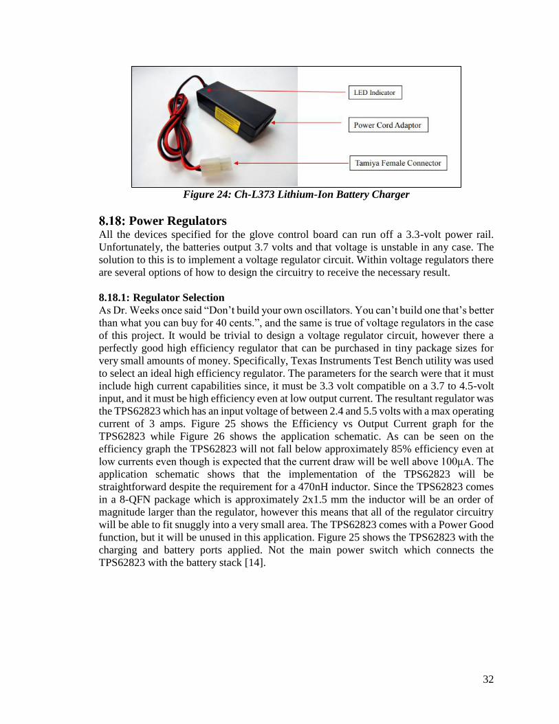
32
Figure 24: Ch-L373 Lithium-Ion Battery Charger
Power Regulators All the devices specified for the glove control board can run off a 3.3-volt power rail.
Unfortunately, the batteries output 3.7 volts and that voltage is unstable in any case. The
solution to this is to implement a voltage regulator circuit. Within voltage regulators there
are several options of how to design the circuitry to receive the necessary result.
8.18.1: Regulator Selection
As Dr. Weeks once said “Don’t build your own oscillators. You can’t build one that’s better
than what you can buy for 40 cents.”, and the same is true of voltage regulators in the case
of this project. It would be trivial to design a voltage regulator circuit, however there a
perfectly good high efficiency regulator that can be purchased in tiny package sizes for
very small amounts of money. Specifically, Texas Instruments Test Bench utility was used
to select an ideal high efficiency regulator. The parameters for the search were that it must
include high current capabilities since, it must be 3.3 volt compatible on a 3.7 to 4.5-volt
input, and it must be high efficiency even at low output current. The resultant regulator was
the TPS62823 which has an input voltage of between 2.4 and 5.5 volts with a max operating
current of 3 amps. Figure 25 shows the Efficiency vs Output Current graph for the
TPS62823 while Figure 26 shows the application schematic. As can be seen on the
efficiency graph the TPS62823 will not fall below approximately 85% efficiency even at
low currents even though is expected that the current draw will be well above 100μA. The
application schematic shows that the implementation of the TPS62823 will be
straightforward despite the requirement for a 470nH inductor. Since the TPS62823 comes
in a 8-QFN package which is approximately 2x1.5 mm the inductor will be an order of
magnitude larger than the regulator, however this means that all of the regulator circuitry
will be able to fit snuggly into a very small area. The TPS62823 comes with a Power Good
function, but it will be unused in this application. Figure 25 shows the TPS62823 with the
charging and battery ports applied. Not the main power switch which connects the
TPS62823 with the battery stack [14].
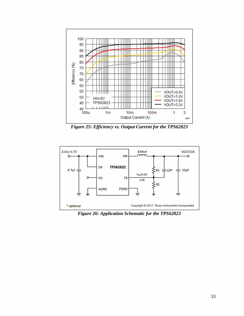
33
Figure 25: Efficiency vs. Output Current for the TPS62823
Figure 26: Application Schematic for the TPS62823

34
Figure 27: Schematic of the TPS62823 with battery ports and charging ports
8.18.2: Timing Regulator
The STM32F030C8 requires that the analog voltage (VDDA) supply is available before the
VDD supply. Since this project will be supplying both voltages from the same rail a timing
regulator was needed to operate a FET switch that would open the 3.3 rail to the VDD supply
after VDDA received power. Essentially the timing circuit will be used as a delay before
powering VDD. The part selected was the MAX6897. This device was selected due to its
small size and convenient supply power requirements. It would be operable from the
battery rail and had a capacitor adjustable external delay. It is also relatively inexpensive
at $1.38 per unit and the design only requires 1. Figure 28 shows the application schematic
while Figure 29 shows the schematic of how the MAX6897 will be implemented with
respect the STM32F030C8 power supplies. The timing delay equation is shown in
Equation 4 and as seen in the schematic in Figure 29 will be set to approximately 60μs
from the 5pF value [15].

35
Figure 28: Application Schematic of the MAX6897
Figure 29: Implementation of the MAX6897 with respect to the STM32F030C8
Equation 4: Timing delay of the MAX6897
Housing The actual housing for the electronics will most likely be implemented as a forearm
mounted box. Inside the box will be the main board which will house the processor, the
regulators, the GPIO controlled switches, the digital to analog converters, etc... Essentially
all electronics except the haptic feedback motors and the Peltier devices will be included
in this board. The batteries will also be included in this housing so for safety the base of
the housing will include a small insulated steel plate. The rational for this is if the Lithium
Ion batteries go into catastrophic failure the steel plate will prevent the user from sustaining
a serious injury. In this case a catastrophic failure may be quite exciting, but it should not
leave the end user with a debilitating injury like sitting on a Galaxy Note 7 might. The
housing will also contain a power switch, a power LED which will display if the battery
needs to be charged or not, a reset button that will calibrate the accelerometers in the glove,

36
a Bluetooth status LED, and a safety shutoff button that will shut off power to all
peripherals.
8.19.1: Light Emitting Diode
As the battery enables power to the system a red LED will enable and remain on until the
power switch is placed back in the off position. This will indicate that the 3.3 Rail is active
and that the power regulator is functioning properly. When the processor finishes booting
it will activate a GPIO pin that will activate an N Channel FET, the BSS138, which will
allow current to the LED. Since both the red, green, and blue LEDs are contained in the
same housing the light emitted will change in purple or another color and this will let the
user know that the glove is now ready for use. The LED selected for this role was the
WP154A4SEJ3VBDZGW/CA manufactured by Kingbright. It is a 5mm tri color LED with
a relatively small package size. It is 9.6 mm in height and has a through hole mount. Each
LED must receive 20 mA to function properly. The following figure shows the tentative
schematic for the circuitry involved in activating this LED. It is a common anode LED
which means that the red, green, and blue LEDs encased in the housing all share the same
positive node. This means, as can be seen in the design that any switching must occur after
the LED as the current moves toward ground. This design will need to be thoroughly tested
in accordance with the test section later in the document. Design changes may be necessary
after testing has concluded [16].
Figure 30: Schematic of LED Control Circuitry
This LED was relatively expensive for an electronic component at $2.05 per unit. Though
since this part is only used once in the project that is acceptable.
Haptic Feedback There are two main options for haptic feedback for our application. Eccentric rotating mass
vibration motors and linear resonant actuators. Both have unique strengths and weaknesses
that will be discussed in the terms of our application. Specifically, we want a small
vibrational device that can fit on a gloved fingertip comfortably and vibrate at various

37
intensities. We are hoping to control this device with either a digital to analog converter or
more realistically the same magnitude control setup we are using to control the Peltier
device.
8.20.1: Linear Resonant Actuators
Linear resonant Actuators or LRAs are a type of vibrational device that operate similarly
to how a headphone or a speaker operates. Specifically, they use a coil to generate a
magnetic field and repulse a rare earth magnet. This repulsion force presses up against a
mass which in turn presses against a spring. By using an AC signal or a pulse width
modulated signal it is possible to drive the LRA to vibrate at some frequency. There are
several downsides to LRAs however. The two most concerning to our application is that
LRAs need pulse width modulated signals or AC signals to operate and that they are very
inefficient when not operated at their resonant frequencies. Creating pulse width modulated
signals or AC signals is trivial however it requires extra hardware and programming that
may not be necessary for what is in effect the simplest peripheral on an already complex
device. Despite this the efficiency issue is more concerning. The resonant frequency is a
frequency of operation at which the impedance of the internal capacitor and winding
inductance is balanced. This results in optimal force being applied to the vibrating mass.
However, when the device is operated at a different frequency then efficiency falls off
dramatically. Our device calls for a range of operational vibrational frequencies and as such
it does not appear that linear resonant actuators are the best fit for our application. They
are much better for haptic response where you want a small package that gives a consistent
vibrational response at a certain frequency, such as cellphone haptics.
8.20.2: Eccentric Rotating Mass Vibrational Motors
Eccentric rotating mass (ERM) vibrational motors are exactly what they sound like. A
small electric motor with an unbalanced weight at the end. The rotation of the weight
generates the vibrations that we perceive as haptic feedback. These devices work exactly
like traditional electric motors. By supplying more voltage, or current depending on the
specifications, we can control the magnitude of the rotation. For our purposes this is
precisely what we need. While it may be natural to imagine ERMs as electric motors with
oddly shaped weights on the end this is only partially true. It may be true that you can
purchase ERMs in that form factor, but that form factor is completely unusable for our
application. Fortunately, coin type form factors and encapsulated form factors are also
manufactured. While encapsulated form factors are not ideal for our applications since they
are essentially the electric motor with a weight but now with a plastic sheathing, the coin
type form factors are perfect for fitting to finger tips. Of course, these aren’t the perfect
component in every way and there are tradeoffs to be made between the coin form factor
and other form factors. Specifically coin form factor ERMs have a higher maximum start
voltage, which is the minimum voltage required to consistently start the motor. Fortunately,
this will not be a major issue since we can account for the higher initial voltage when
designing the control circuits for the haptic response.
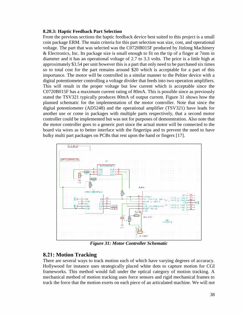
38
8.20.3: Haptic Feedback Part Selection
From the previous sections the haptic feedback device best suited to this project is a small
coin package ERM. The main criteria for this part selection was size, cost, and operational
voltage. The part that was selected was the C0720B015F produced by Jinlong Machinery
& Electronics, Inc. Its package size is small enough to fit on the tip of a finger at 7mm in
diameter and it has an operational voltage of 2.7 to 3.3 volts. The price is a little high at
approximately $3.54 per unit however this is a part that only need to be purchased six times
so to total cost for the part remains around $20 which is acceptable for a part of this
importance. The motor will be controlled in a similar manner to the Peltier device with a
digital potentiometer controlling a voltage divider that feeds into two operation amplifiers.
This will result in the proper voltage but low current which is acceptable since the
C0720B015F has a maximum current rating of 80mA. This is possible since as previously
stated the TSV321 typically produces 80mA of output current. Figure 31 shows how the
planned schematic for the implementation of the motor controller. Note that since the
digital potentiometer (AD5248) and the operational amplifier (TSV321) have leads for
another use or come in packages with multiple parts respectively, that a second motor
controller could be implemented but was not for purposes of demonstration. Also note that
the motor controller goes to a generic port since the actual motor will be connected to the
board via wires as to better interface with the fingertips and to prevent the need to have
bulky multi part packages on PCBs that rest upon the hand or fingers [17].
Figure 31: Motor Controller Schematic
Motion Tracking There are several ways to track motion each of which have varying degrees of accuracy.
Hollywood for instance uses strategically placed white dots to capture motion for CGI
frameworks. This method would fall under the optical category of motion tracking. A
mechanical method of motion tracking uses force sensors and rigid mechanical frames to
track the force that the motion exerts on each piece of an articulated machine. We will not

39
discuss mechanical tracking in any detail since as its name implies it is a mechanical
structure and this is the Electrical and Computer Engineering Senior Design Course. A
mechanical solution could even be optimal but would fail to demonstrate our mastery of
electrical and computer engineering skills. Finally, inertial systems use a variety of
electronic sensors to capture motion data. This data is usually wirelessly transmitted to a
receiver where it is analyzed by a computer where it is processed into useable and
understandable structures.
8.21.1: Optical Tracking
Optical tracking methods use cameras and reflective or light emitting nodes at various
points to track motion. This is a high accuracy method since specialized high-speed
cameras can achieve extremely high frame rates that can then be easily filtered to isolate
the nodal motion from the reflective or light emitting nodes. This is the most commonly
used method of motion tracking for consumer devices. For example, Hollywood uses high
speed cameras, the Xbox Kinect uses an infrared camera and pulses of infrared light to
track motion, and even the Nintendo Power Glove used high frequency sound and audio
recovers to track its position using the Doppler Effect. While it would be possible to use
this type of tracking scheme to interact with a 3D object, in order to receive haptic and
temperature feedback almost all of the circuitry and I2C communication in the glove would
still be required. It would also be very much a “me too” project that emulated existing
commercial hardware and at that point why even bother developing our own motion
capture system?
8.21.2: Inertial Sensors
Inertial sensors are a wide array of different sensors that capture motion of one kind or
another. Common types of sensors include accelerometers, gyroscopes, and magnetometer.
The main selling point of inertial sensors are that they require no external cameras or bulky
equipment and are therefore popular with small self-contained devices and certain
scientific equipment. For instance, in several of the microgravity labs at UCF
accelerometers and gyroscopes are the only practical choice for data collection because it
is impossible to fit bulky cameras or large force sensing equipment onto a rocket. We will
be discussing accelerometers particularly in depth.
Accelerometers measure acceleration as the name would imply. They do this be measuring
the force of motion exerted on an object of known mass. Newton’s Second Law tells us
that force is a function of mass and acceleration while Newton’s First Law tells us that an
object at rest will remain at rest until an outside force act upon it. Finally, Newton’s Third
Law tells us that when one body acts upon another with a force, that second body will
excerpt an equal and opposite force upon the first. With this information it is possible to
calculate the acceleration of an object in a single plane from force by placing a small
passive force sensor in that plane and allowing the force of the motion acting upon some
small object of known mass. This allows us to back calculate wit very simple algebra the
acceleration of the motion that generated the force. Of course, there are several methods
for measuring the magnitude of the force.

40
There are two main methods for measuring the magnitude of a force in an accelerometer.
The first uses capacitance to accurately characterize the magnitude of force applied. It is
possible to do this because as the force upon the mass increases the capacitive plates are
forced more closely together. This changes the total capacitance in the system which has
an easily measurable response in any electronic system.
The second method for measuring the magnitude of a force in an accelerometer is to use a
piezoelectric sensor. This type of accelerometer takes advantage of the piezoelectric effect.
The piezoelectric effect is that when certain materials have mechanical stresses applied to
them they generate an electrical charge or when those same materials have an electrical
field applied to them they generate a mechanical change. Quartz in quartz watches are the
most famous and commonly known example, but other examples may include crystal
oscillators or inkjet printer heads. Essentially piezoelectric devices can be found anywhere
that electrical systems need to control small mechanical motions.
8.21.3: Accelerometer Considerations
In our search for exactly the right accelerometer we needed to consider several aspects of
the device. Our first consideration was the size of the device. It must be small enough to
easily fit onto the tip of a finger along with several other components. The next aspect we
had to consider was the price. It is quite possible to get some amazing high-quality
accelerometers for precision scientific work, but those are expensive and we are not doing
high quality precision work. We are developing what is essentially a consumer product.
So, to stay within budget a cheaper model must be found since it will most likely not impact
the end results of the project. The next aspect of the accelerometer we had to consider was
it operable range. Many accelerometers have certain operable range settings where it is
most accurate. Exceeding these range settings may mean you will not get useful or meaning
full readings. For our application this was easy since hand motions will tend to stay in the
±2 G range. Any more than that will mean that the user is wildly and forcefully flailing
their hands around which should be discouraged. The next aspect we must consider is the
precision of data the device can record. These devices send out digital signals from an
analog data source so they must have internal analog to digital converters. The number of
bits they can record determines their level of sensitivity. We would like at least 8 bits of
precision since that its 1 ASCII character and if we must read data from the device it will
have to be in packets of 8 bits anyway. An often-unconsidered aspect we need to discuss
is the data capture rate. We need to be able to sample at hard minimum of a 30 Hz sampling
rate. Though it would be better to have a much higher rate than that. Another aspect to
consider is the communication protocol the device uses. There are usually several different
communication protocols to choose from depending on what you want to achieve We wish
to use I2C since we want to communicate with several devices on the same data line and
so the accelerometer we choose must be I2C enabled. Finally, we need the accelerometer
to have a purchasable testing board so that we can test and implement our driver code
without having to integrate the entire device beforehand.
8.21.4: Accelerometer Choice
In the end after carefully considering all the aspects listed in the previous section we have
decided to implement the MMA8451Q, 3-axis, 14-bit/8-bit digital accelerometer from

41
NXP Semiconductors. Table 6 has a list of features that make this board desirable for our
needs [18].
Feature MMA8451
Max Sampling Rate 800 Hz
Communication Interface I2C
Multiple Addresses Yes, 2
Data Resolution 14 Bit
Package Size 3mm x 3mm x 1 mm
Price $3.34
Breakout Board Yes, from Adafruit
Table 6: Features of the MMA8451
As can be clearly seen from Table 6 the MMA8451 is very good for our application. Figure
32 shows how the chip must be applied in our circuit to function properly.
Figure 32: Implementation Diagram of the MMA8451Q
8.21.5: I2C Multiplexer
Since the MMA8451Q has only two possible addresses and the project requires 16
accelerometers an I2C multiplexer must be implemented. As referenced in Figures 3 and 4
the accelerometers and peripherals will be placed on 1 of 8 possible I2C lines. The part
selected was the TCA9548A from Texas Instruments. The TCA9548A has 8 pairs of
multiplexed I2C lines as shown in Figure 33. The TCA9548A can run on a 3.3-volt power
supply and has a small package size at 7.8 x 4.4 mm. It can handle up to a 400 kHz clock
frequency and all I/O pins are tolerant to 5 volts. Figure 34 shows the application schematic

42
for the TCA9548A. Note that external pullup resistors are required, which is standard in
I2C. Pullup resistors will be 1 kΩ which is near the minimum resistance specified by the
data sheet [19].
Figure 33: Simplified Block Diagram of the TCA9548A
Figure 34: Application Schematic of the TCA9548A
Final Hardware Implementation The final hardware implementation was remarkably unchanged from the previous design
document. The only direct hardware issue that was discovered on attempting to demo was
that the I2C lines needed to be attached to pins 35 and 36 respectively. The performance
of the device could have been improved by the addition of a gyroscope and a magnetometer

43
to more accurately track yaw of the hand and the position of the hand relative to the ground.
To streamline the code development process, the hardware was reduced to 1 vibrational
motor and 2 accelerometers. This removed the I2C mux that had been used to access all
the various I2C lines, however it appears the issue with the I2C mux was a coding error so
the mux could be easily implemented under the current scheme. The final demonstration
was done with a single I2C line with two accelerometers and a single feedback motor. This
was done to demonstrate proof of concept since any additional accelerometers and
feedback devices would only add aditional fingers to the model.
9: Processing Board Overview The MITTS (Motion Interface Thermal Touch Sensitive) device has a central processing
board that handles data gathering and delivery. This board handles data needed from the
43 sensors on the glove such as the accelerometers. It also controls the haptic response to
the vibrational motors and Peltier devices for both resistive sensation and temperature
changes. This board contains a Bluetooth device to send data through the UART standard
to a computer for further data manipulation and processing.
Processor Comparisons According to Umesh Lokhande’s article on the BinaryUpdates website [20], he writes that
some good parameters to look for and take into consideration for a microcontroller are:
whether there are good resources available, whether it’s economical, and whether it’s easy
to program.
Having good resources to understand our project more was a huge plus, especially for this
design since we are working with things we haven’t worked with before and trying to
assemble a whole project with them. Hobbyist communities have step-by-step tutorials
using the ATmega series and TI’s MSPxx series, which makes them exceptional choices.
However, these are not widely used in big manufacturing and/or MCUs designed for
specific applications. For this reason, we wanted to go with an ARM device due to their
wide use in the industry.
The ATmega series [21] and TI’s MSPxx series [22] has a wide variety of cheap options
in comparison to an ARM MCU but are slightly more expensive. While looking at the
Mouser Electronics website for comparisons, the ATMEGA32U4-AU is more expensive
with a comparison of $4.80 for a single unit whereas the STM32F030C8T6 ARM chip [23]
is $2.02 for a single unit. The ATmega also has less I/O pin count than the ARM chip; the
ATmega being at 26 I/O pins and the STM being at 39 I/O pins. The ARM chip also
operates at a lower voltage with a 2.4-3.6 V compared to 2.7-5.5 V. As far as the TI MSPxx
series goes, looking at a similar pattern, the MSP430G2553IPW28 is $2.59 for a single
unit, has only 24 I/O pins, and fortunately operates at 1.8 – 3.6 V. The difference
economically makes sense here since the STM32F030C8T6 is cheaper, has more I/O pins,
and is decently low in voltage operation.

44
MCU Cost I/O Pins Operating Voltage (V)
ATMEGA32U4-AU $4.80 26 2.7-5.5
MSP430G2553IPW28 $2.59 24 1.8-3.6
STM32F030C8T6 $2.02 39 2.4-3.6
Table 12: MCU comparison Data According to the Mouser Website
I/O Pins - The number of I/O pins on the STM is greatly higher than that of the ATmega
and MSP chip. This choice of picking the STM will allow the design to add more input
and/or output devices if further development were to occur. This concept is great for
scalability
Memory Size - All three MCUs have FLASH memory have a non-volatile memory. Since
the coding will be relatively simple, it should only need a little bit of memory to handle
getting input and then sending that input off to something else. In this case, it sends to a
computer through a Bluetooth module, so memory is not an issue there.
Chip Memory Size (kB) Data RAM Size (kB)
ATMEGA32U4-AU 32 2.5
MSP430G2553IPW28 16 .512
STM32F030C8T6 64 8
Table 13: Memory Comparison Data According to the Mouser Website
As we can see from the table above, even though the STM is the least expensive, it has the
most memory in both regards. Clearly, this is an economical and logical choice.
Clock Frequency - As the project design looks to keep a frame rate of 30 frames per second,
the speed that the clock needed to be isn’t too significant, especially in today’s standards.
Chip Max Clock Frequency (MHz)
ATMEGA32U4-AU 16
MSP430G2553IPW28 16
STM32F030C8T6 48
Table 14: Clock Speed Comparison According To The Mouser Website
Again, even though it’s the cheaper option, this chip has a much higher (3 times higher)
clock frequency than the other ones have. In the next figure, there is the details of the pinout
of the chip itself. This came in handy when integrating the circuit into the design. Knowing
the pinouts on the board itself is essential in connecting components and assisting in the
overall schematic design.

45
Figure 35: STM32 Pinout
9.1.1: The STM32F030C8T6
As a brief overview, the STM implements ARM, which is widely used in commercially
manufactured products today, thus provided us with real-world applicable experience. This
experience gave us an edge on the job market and put us ahead for a potential career choice.
Not only is the chip applicable, but it’s a smart economical choice and will be very useful
and efficient in our project. With high frequency rates and low cost, this chip was the best
choice.
Multiplexers - There is one caveat to the STM32 and that is that there are not enough I/O
pins on the board for us to read from the output to the devices on the glove. For this reason,
rather than upgrading to a higher priced and bigger chip, we made use of multiplexers. This
drastically decreased the number of I/O pins necessary. Since we can use a 3-8 or 4-16
multiplexer, we ended up using only 4 or 5 pins for input into the chip and selection pins
into the multiplexer. We made use of the polling strategy in our case because of the high
frequency of the chip and the easy 30 frames per second that we were trying to achieve.
STM32 Breakout Board - The design heavily relies on the STM processing board for
further development. The 3D interface relies on the processor to give it the details of the
accelerometers. The interface between the 3D interface also relies on this data. All of the
glove components rely on the processor, not only to read data from them, but also to send
data to them. For this reason, it was very beneficial to get a breakout board, which
essentially acted as the processing board since it uses the same chip. The exclusion of
course will be that the board itself was not the exact design, so things changed from the
development to the physically made device. The coding, however, stayed the same since
the pinout is the exact same on the development board as to the chip that we’ve selected.
The trick will be to map those to our components when designing the schematic.

46
Requirements and Specifications Fulfillments
1. The processor is an ARM chip.
2. The processor has low-power capabilities, thus can fulfill the low-power
consumption.
3. The processor has at least 1 dedicated I2C line
4. The clock frequency is 48 MHz so 30 frames per second specification is achievable.
5. We can add hardware options to fulfill the power switch and reset option
capabilities.
Input and Output through Processor The processor must deal with a lot of input and output. There are 6 vibrational motors, 6
Peltier devices, 16 accelerometers, and a computer communicating with or through the
processor board. With this, the chip needed to be fast enough to poll and control each motor
and sensor as well as communicate through the Bluetooth module to communicate with the
computer for further processing of data.
Figure 36: Data Flow Schematic of The Glove
As we can see from the design above, the design doesn’t even see the Blender module.
Also, it doesn’t even see the components of the interface or of the glove design. In this
way, the processor only needs to know what input it will get from the accelerometer, what
feedback it needs to give back to the glove design, and what input and output to expect
from the interface. Something that needs to be communicated is the format of the data
that’s expected for the interface. As far as the accelerometers, they are rather set due to the
design given to them, but the interface is completely arbitrary.
I2C - Communication on a wire can be tricky. If everything is trying to communicate at
once to the processing board, then the board will not understand what is communicating
with it. For this reason, there are protocols that can be used to that communication goes
smoothly. According to i2c.info [24], “The system must be designed in such a way that
slower devices can communicate with the system without slowing down faster ones.” For

47
our sensors and modules, we connected them on a bus, so we didn’t have hundreds of
individual wires wasting a single line, when we can easily communicate on a single bus.
This is essentially what the I2C is, an Inter-Integrated Circuit bus. The i2C website
clarifies, “A bus means specification for the connections, protocol, formats, addresses and
procedures that define the rules on the bus. This is exactly what I2C bus specifications
define.” The site continues to define what I2C is by listing things such as terminology, bus
signals, serial data transfer, start and stop condition, I2C data transfer and even more
terminology.
UART - This method of communication, which stands for Universal Asynchronous
Receiver/Transmitter, is a means to simplify and aid in data communication. According to
the website All About Circuits [25], UART uses only three signals: Tx (transmitted serial
data), Rx (received serial data), and ground. It continues to say that there is no need for a
clock signal because the internal clocks of the receiver and transmitter will ensure that the
proper timing is done internally. Some requirements for UART say that the clock signals,
“… must be sufficiently accurate relative to the expected frequency and sufficiently stable
over time and temperature.” We used this protocol for communication with our Bluetooth
module. Here are some key terms, like I2C, that are used by UART, which are taken from
the All About Circuits website:
1. Start bit: The first bit of a one-byte UART transmission. It indicates that the
data line is leaving its idle state. The idle state is typically logic high, so the
start bit is logic low.
2. Stop bit: The last bit of a one-byte UART transmission. Its logic level is the
same as the signal’s idle state, i.e., logic high. This is another overhead bit.
3. Baud rate: The approximate rate (in bits per second, or bps) at which data can
be transferred. A more precise definition is the frequency (in bps)
corresponding to the time (in seconds) required to transmit one bit of digital
data.
4. Parity bit: An error-detection bit added to the end of the byte. There are two
types: “odd parity” means that the parity bit will be logic high if the data byte
contains an even number of logic-high bits, and “even parity” means that the
parity bit will be logic high if the data byte contains an odd number of logic-
high bits.
With this protocol in place, keeping everyone informed about which start bit and stop bit
was be using was important. The baud rate is typically 9600 baud, at least in typical
Arduino tutorials, but we used 115200. With this information, we had a seamless
transmission of data between the processing board and the Bluetooth module.
Input from Accelerometers - The input from the accelerometers has 3 different types: the
x-axis, the y-axis, and the z-axis. All three of these components have 14-bits that needed
to be read for an accurate reading. That’s a total of 42-bits that needed to be read for each
accelerometer. If there are 16 accelerometers, then it needed to read a total of 672 bits.
Since it needed to store them in 8-bit increments, that means we stored each 14-bit in a 16-
bit frame. Thus, we had a total of 48-bits (6 bytes) per accelerometer. Again, with 16

48
accelerometers, we had 768-bits to store all of our inputs from accelerometers, which is a
total of 96 Bytes.
Wireless Communication For the setup, we went with Bluetooth communication. However, there are a plethora of
ways to send data wirelessly, ways that include: infrared, satellite, radio waves, Bluetooth,
Wi-fi, and many other methods as well.
9.3.1: Pros and Cons of Wireless Communication
According to the website elprocus.com [26], some advantages of wireless communication
include fast speeds, fewer materials and overall less cost. For us, the biggest pro of having
wireless is since our system is convenient if the user is not connected to a bunch of wires.
Being wireless allows the user to free up degrees of movement.
The disadvantage mentioned by the elprocus.com website is that data transmission is not
as secure. However, for us, we are not transmitting anything that would be of value since
48 the data is only going to be pertaining to accelerometer values. On the other hand, we
are getting input data, so if a hacker were trying to send in values to would cause the Peltier
devices to heat up drastically, that could pose a problem. We have already thought of this.
In this case, we will be hard-coding into the processor limiting values. With these limiting
values, no matter what data is sent in, the Peltier device wouldn’t get hotter than whatever
temperature we’ve set the limiter at.
9.3.2: Bluetooth Module Choices
Bluetooth has been growing in popularity ever since headsets started to make use of the
technology, in my own opinion. Bluetooth is convenient; it has a very simple setup and
compatible. The setup only requires that one scans for other devices and one is set to be
discoverable. As far as compatibility is concerned, if both modules have a Bluetooth
module, then they will work together, as long as they are within the correct version of
course. For example, most Bluetooth x.x are compatible with each other, but the Bluetooth
5 is not backwards compatible with 4.0, or 3.0, but the 4.0 is compatible with the 3.0. Here
is a brief overview of the different versions of Bluetooth:
Basic Rate
(BR)
Enhanced
Data Rate
(EDR)
High
Speed
(HS)
Low
Energy
(LE)
Slot
Availability
Masking
(SAM)
Bluetooth 1.x Yes No No No No
Bluetooth 2.x Yes Yes No No No
Bluetooth 3.x Yes Yes Yes No No
Bluetooth 4.x Yes Yes Yes Yes No
Bluetooth 5.x Yes Yes Yes Yes Yes
Figure 37: Bluetooth Comparison Table

49
Of course, we most likely wanted to choose a Bluetooth with a version of at least 4.x or
higher since most devices now-a-days has this technology and for its speed and low energy.
RN4871-V/RM118 [27] - This Bluetooth module is 9x11.5 mm and is Bluetooth 4.2. It is
shielded which will aid in short-prevention and overall integrity and strength of the design.
It’s small enough to help in fitting all the components onto a single PCB design and still
fitting onto a wrist. This module also supports UART, which is the type of protocol we are
designing the PCB to use to transmit data. This module also has an antenna on the chip.
BL652-SC-01 [28] - This Bluetooth module is 120x93 mm and is also Bluetooth 4.2. The
data sheet does not specify any shielding, but from the looks of the image, the components
on the board look enclosed. It’s a bit bigger than the other module, which may become a
problem if we don’t have enough space, but still rather small. This has a larger selection of
interfacing protocols, which still includes UART. The antenna is external rather than on-
chip.
BM62SPKS1MC2-0001AA [29] - This Bluetooth module is 29 mm x 15 mm x 2.5 mm
and is also Bluetooth 4.2. The module is shielded, which again will help with the space on
our PCB. This module also supports data transmission over the UART interface. The
antenna is stated to be on-board.
Traits RN4871 BL652 BM62SPK
Cost $8.44 $7.45 $12.50
Shielding Yes Yes Optional
Antenna Chip On-board On-board
Size (LxW mm) 9x11.5 120x93 29x15
Operating Voltage (V) 1.9 – 3.6 1.8 – 3.6 3.2 – 4.2
Supply Current Receiving (mW) 10 5.4 unknown
Supply Current Transmitting (mW) 10 5.3 unknown
Table 15: Bluetooth Module Comparison Taken from Mouser.com
As we can see from the table above. The BL652-SC-01 seemed to be the best option. Not
only did it cost the least amount of money, at least on this website it does, but it also seemed
to use the least amount of power. Of course, with that we probably lost some distance in
which we can transmit data, but the use-case for our device was strictly within a room next
to the computer that will be taking in the data transmission so that would not be a problem.
The next image is that of the schematic for the BL652 Bluetooth module. This gives a
visual representation of the pinout of the design and will assist in the design process when
integrating the circuit into the design.

50
Figure 38: Pinout of BL652
Figure 39: Image from EL652-SC-01's data sheet about OEM Responsibility
From the image above, they give specific outputs and antenna to comply the regulatory
guidelines. Included in the data sheet is also more OEM responsibilities, which OEM
stands for Original Equipment Manufacturer. The image below shows these
responsibilities:
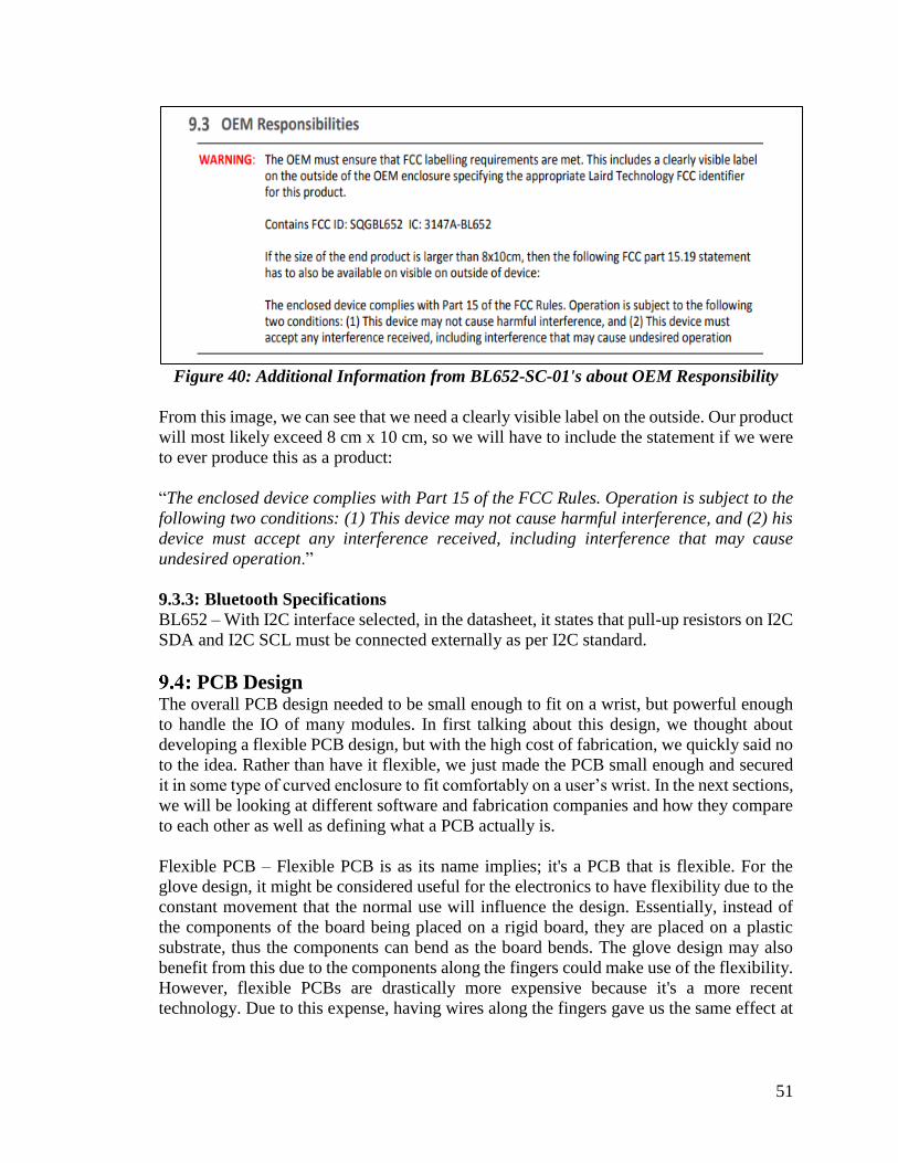
51
Figure 40: Additional Information from BL652-SC-01's about OEM Responsibility
From this image, we can see that we need a clearly visible label on the outside. Our product
will most likely exceed 8 cm x 10 cm, so we will have to include the statement if we were
to ever produce this as a product:
“The enclosed device complies with Part 15 of the FCC Rules. Operation is subject to the
following two conditions: (1) This device may not cause harmful interference, and (2) his
device must accept any interference received, including interference that may cause
undesired operation.”
9.3.3: Bluetooth Specifications
BL652 – With I2C interface selected, in the datasheet, it states that pull-up resistors on I2C
SDA and I2C SCL must be connected externally as per I2C standard.
PCB Design The overall PCB design needed to be small enough to fit on a wrist, but powerful enough
to handle the IO of many modules. In first talking about this design, we thought about
developing a flexible PCB design, but with the high cost of fabrication, we quickly said no
to the idea. Rather than have it flexible, we just made the PCB small enough and secured
it in some type of curved enclosure to fit comfortably on a user’s wrist. In the next sections,
we will be looking at different software and fabrication companies and how they compare
to each other as well as defining what a PCB actually is.
Flexible PCB – Flexible PCB is as its name implies; it's a PCB that is flexible. For the
glove design, it might be considered useful for the electronics to have flexibility due to the
constant movement that the normal use will influence the design. Essentially, instead of
the components of the board being placed on a rigid board, they are placed on a plastic
substrate, thus the components can bend as the board bends. The glove design may also
benefit from this due to the components along the fingers could make use of the flexibility.
However, flexible PCBs are drastically more expensive because it's a more recent
technology. Due to this expense, having wires along the fingers gave us the same effect at

52
52 a much cheaper price. Furthermore, the PCB design was mounted on the wrist, thus we
made use of bands to mount the device to the wrist of the user.
Flexible PCB over Rigid PCB – Continuing further, we chose a rigid PCB due to the high
cost of the flexible PCB. The wires connecting the components on the glove design are
much cheaper but brought a bigger design overall since wires on flexible PCB are smaller
than individual wires connected to each component. Moreover, flexible PCBs are an
overdesign for the design we were trying to make. Simpler is sometimes easier.
9.4.1: Schematic Design Tools
In order to fulfill the design requirements, there needs to be a PCB design. For this to take
place, the PCB needs to be designed. There is an extensive list of design tools that are for
freelancers all the way to big industry. Some come with a heavy price tag, which includes
engineers ready to help in the design process, and some are free with tutorials and
documentation to guide users along. Since the design only consists of a single PCB and its
details are rather simple, a free version of a schematic design tool, will do the job. In the
next few paragraphs, there will be schematic design tool options.
9.4.2: KiCAD
For designing the PCB, we will be using KiCAD, which is a free software suite for
electronic design automation. The reason we will be using KiCAD is that it’s open-sourced,
which means it’s free, and it being open-sourced means we are staying true to our design
goal of making our own project open-sourced. When traversing through the site, there is a
“Help” menu, which provides a plethora of documentation at our disposal as well as
tutorials. We would benefit most from this software mainly because we have had
experience using it, and throughout this design, experience will get us a lot further than
education.
9.4.3: SOLIDWORKS PCB
According to the Trimech website [30] , SOLIDWORKS PCB boasts being powered by
Altium’s best-in-class PCB technology. Altium seems to be a technology all on its own.
This leads me to believe that SOLIDWORKS PCB is more of a framework to allow
integration between the PCB design and the mechanical design of using SOLIDWORKS.
It continues to say that it integrates seamlessly with SOLIDWORKS, which enables a
completely collaborative electro-mechanical workflow, so my assumption of if it’s more
of a framework seems to be correct. This sounds enticing; however, we are not going to
have a mechanical design complex enough to be using software to create it, so this choice.
9.4.4: DesignSpark PCB
The rs-online website [31] which hosts the DesignSpark software states that the software
doesn’t have limitation on design schematic size as well as integration into their other free
software that “take your brightest ideas all the way through to final production.” You can
also use as many layers, pads, nodes, and connections in your design as you’d like. A cool
part of this software is if you can’t find a part to put into the PCB design, then their software
has a functionality that allows you to create them from PCB Part Library. This functionality
seems very useful.

53
PCB Fabrication Eventually, when the design is finished, the design needs to be created. To do this, one can
develop their board and buy a bunch of industry equipment and essentially 3-D print the
board oneself, or like most people, going to a PCB fabrication company will save lots of
money. In the next couple of paragraphs, researched options will be listed, and their details
will be explained.
9.5.1: PCBWay
PCBWay [32] is a full feature custom PCB prototype service. They boast a low-cost
fabrication and a quick delivery time. A basic design that’s within 100 mm x 100 mm and
10 pcs is estimated at $5.00, which is an incredible price. It also states that the design would
only take 2-3 days, which is rather typical for small-batch PCB fabrication.
9.5.2: 4pcb
4pcb [33] does their production in the United States. This can be seen as a benefit, but most
likely their design will be more expensive, but with less shipping costs. Their website
doesn’t give an estimated price for anything, but they do provide this chart:
Figure 41: PCB Specification Comparison [33]
From this chart, we can see that their layer count and turn-time is around the same as
PCBWay, but they don’t include an estimated price as PCBWay does. From this we can
speculate again that PCBWay will have higher shipping cost because they are shipping
from China, but with a lower design cost and 4pcb will have a lower shipping cost because
54 they produce

54
9.5.3: PCBgogo
The PCBgogo [34] website boasts a 12-24-hour quick turn PCB prototype service, which
is very quick. They also have a low minimum from 1 pcs PCB Assembly is accepted, which
I don’t believe we will actually benefit from or need. They boast 24-hour customer service
availability, which could come in handy if we have any questions. A big plus in my book
is the fact that they have 99% on-time DHL Delivery so if we are not very unlucky, we can
typically trust in the delivery time that they set, which could come in handy in a time
crunch. A professional PCB engineer one-to-one service is offered. This fabrication
company seems to be very trustworthy and helpful and would be a good alternative to
PCBWay.
9.5.4: JLCPCB
The JLCPCB [35] website advertises the lowest prices for PCB design researched. They
boast over 200,000+ customers worldwide and 8000+ online orders per day. They claim to
be the largest PCB prototype enterprise in China. They specialize in quick PCB prototyping
and small-batch production, which is exactly what the design entails. The only downside
to this choice would be, like most others, is that it ships from China, which can take a long
time. However, they state only up to 2-3 days of build time and shipment tracking, which
can ease tension in a build when waiting on parts.
PCB Design Constraints There is a plethora of constraints to consider in the PCB design, some are already included
when we considered the Bluetooth module from earlier. Constraints can come in a variety
of broad topics such as: environment, economical, sustainability, social, political, ethical,
manufacturability, and most importantly, health and safety. In further reading, we will
cover constraints within each category and explain each constraint that is arbitrarily placed
on our project, or a constraint due to reasons out of our hands.
9.6.1: Environmental Constraints
Environmental constraints can be constraints given to us by the environment around us,
such as, we cannot create a design that is bigger than a room, because a user is intended to
us it within a room. That’s, however, a broad example that didn’t need to be addressed due
to the nature of our project. Environmental constraints can also be given to us by literal
protocols or regulations required due to the environment, such as waste produced by a
product and how it’s disposed of or even the amount of carbon dioxide that a product can
produce.
We didn’t have any environmental constraints on our project, but we included
Lithiumpowered batteries, which can pose a hazard to the environment if disposed of
properly. This isn’t necessarily our responsibility due to the batteries including labels on
them that inform the user to dispose of the batteries properly.
9.6.2: Economical Constraints
Economical constraints are constraints that talk about costs, efficiency, and can even
include longevity because the longer the product can less, the more economical it is. For
the PCB design, our economical constraints were only to make the design cheap to make

55
an impact for future hobbyists to tinker with our design. For that to happen, we made the
board, low-powered, use low-cost modules, and cheap to manufacture.
9.6.3: Sustainability Constraints
Sustainability constraints are essentially constraints to allow further development of our
design over a long period of time. For example, if the chip that we chose decides to be
discontinued and no longer manufactured for whatever reason, then our design will no
longer be sustainable. For this reason, we had an obligation to keep the design sustainable,
so hobbyists can use the design in the future. In this way, we tried to use up-to-date
technology, like choosing a 4.x Bluetooth module rather than 1.x or 2.x and making our
design rather simple to change. If our design is simple, a part can be changed without
affecting too many other parts, essentially making everything loosely coupled.
9.6.4: Social and Political Constraints
Social and political constraints are closely related. Social constraints are constraints
enforced by society and political constraints are constraints enforced by policy. In the PCB
design, there are no constraints based on these topics.
9.6.5: Ethical Constraints
Ethical constraints are constraints that are imposed by ethical dilemmas or forced due to
ethics of society. The only ethical constraint that we had on our design was to make it cheap
for the open-sourced community so that they can learn and tinker with our design without
breaking their bank.
9.6.6: Health and Safety Constraints
Health and Safety constraints are imposed by either regulation and requirements. These are
regulated because a lot of technology today can be dangerous and if standards aren’t met,
then people can become injured. The first thought we had about our PCB design was
concerned about shock risks, sharp-object risks, and temperature risks. The shock risks can
come from the PBC design coming into contact with the user. For this, we put the PCB
design on wood so contact with the skin can’t be made. For the sharp-object risks, it’s
solved by being on the wood. The risk was that usually sharp wires from soldering or from
the design can stick out and are rather sharp. With the wood, no contact can be made with
the wires. The heat risk can be reduced by implementing a heat sink on the chip as well as
using an enclosure to keep the design further away from the user. The battery was likely
be the highest temperature and, since it’s lithium, has a higher risk of catching of fire or
even exploding. For this reason, we will also include a metal enclosure for the battery that
will act as a fire/explosive defense measure.
System Startup Procedure When the processor design initially gets power, there needs to be a couple of events that
occur. These events included visual cues of the device turning on, data being read, pins 56
being set, and then a loop of reading and sending data with the Blender interface and the
glove components. The next figure will show a coding block diagram of how this procedure
will work. Initially, the device will get power. To indicate this, it’s programmed a red LED
to light up to signify that the device is booting up. During the chip boot, a few events occur
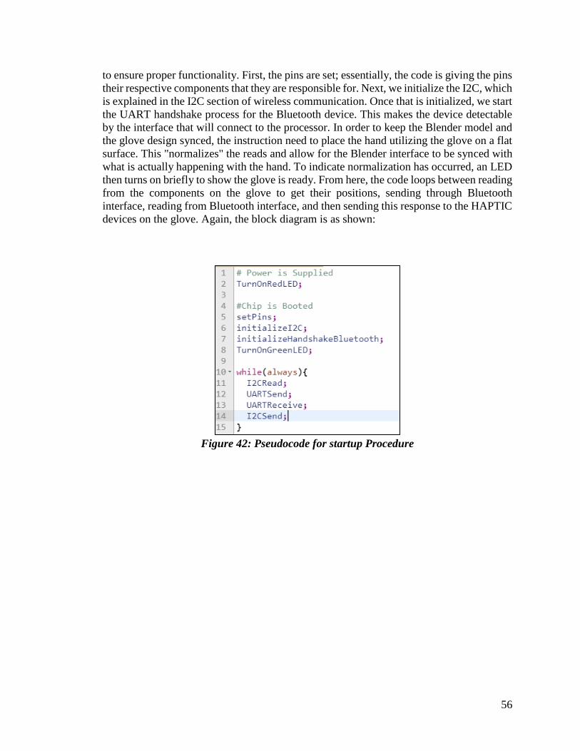
56
to ensure proper functionality. First, the pins are set; essentially, the code is giving the pins
their respective components that they are responsible for. Next, we initialize the I2C, which
is explained in the I2C section of wireless communication. Once that is initialized, we start
the UART handshake process for the Bluetooth device. This makes the device detectable
by the interface that will connect to the processor. In order to keep the Blender model and
the glove design synced, the instruction need to place the hand utilizing the glove on a flat
surface. This "normalizes" the reads and allow for the Blender interface to be synced with
what is actually happening with the hand. To indicate normalization has occurred, an LED
then turns on briefly to show the glove is ready. From here, the code loops between reading
from the components on the glove to get their positions, sending through Bluetooth
interface, reading from Bluetooth interface, and then sending this response to the HAPTIC
devices on the glove. Again, the block diagram is as shown:
Figure 42: Pseudocode for startup Procedure

57
Figure 43: Block Diagram for Startup Procedure
10: Relevant Technologies Some may argue that every new idea is simply a combination of other ideas. With the
advent of virtual reality and augmented reality, an industry of haptic feedback popped up
into the world. While there are certainly technologies out there that have accomplished
haptic feedback, our design is unique because of the way we are incorporating the sense of
touch and temperature.
Existing Technologies and Products In the next couple of sections, there are some technologies that are alike to the design being
created. These designs offer either higher quality, a more specific feedback system or even
a lower quality or a higher price.
10.1.1: VRGluv
The VRGluv [36] is a force-feedback system that uses pulley like technology to pull the
fingers back to make the user feel like they are grabbing an object and can't close their hand
anymore. They have 10-zones of feedback on each hand, which can provide 5 pounds of
force to simulate rigid objects. They express 10-ms of latency over wireless
communication. They also claim 360-degree thumb tracking. Some obvious similarities
are that both designs have a force feedback and wireless communication. Our haptic glove
design is different in the manner that the design gives force feedback; rather than have

58
something pull at the user's fingers, we are giving a rumble affect to show that you are
touching something. Also, we are incorporating a temperature-feedback design which isn't
present in the VRGluv.
10.1.2: HAPTX
HAPTX [37] is a more complex design on the market today. They have a patented
microfluidic technology that lets you feel the shape, movement, texture, and temperature
of digital objects. This technology also claims 5 pounds of force feedback with what seems
to be the same design choice of the VRGluv. It also has industrial grade motion-tracking.
To compare, our glove won't give a sense of shape or movement of an object. With our
design, it's much simpler. We are giving temperature feedback as they do, but their design
is much more complex. We also will have "industrial" grade motion-tracking due to each
finger have 3 accelerometers. Judging from the images, our design seems like it will be
less cumbersome and most likely, considerably cheaper to produce. However, with the
cheaper product, the quality of the feedback doesn't seem like it will compare to the
technology that they are incorporating into their design.
In the following table, we will consolidate the functions and features of the aforementioned
products on the market today compared to our design.
Features MITTS VRGluv HAPTX
Force Feedback No Yes Yes
Temperature Feedback Yes No Yes
Motion Tracking Yes Yes Yes
SDK Provided No No Yes
Low Latency Yes Yes Yes
Pressure Sensing Yes Yes Yes
Texture Feedback No No Yes
Table 16: Product Comparisons
As we can see from the table above, the HATPX is by far the most functional. The MITTS
design is sacrificing quality for a lower cost and cheap production.

59
Programming the Chip For the components to work properly, the chip needs to know what to do and for it to know
what to do, we needed to program the chip. The chip the design used doesn’t have an
unlimited amount of memory, so it was going to be best to program it with a low-cost to
memory. In general, the lower-level the language, the lower amount of memory will be
consumed. The highest level typically used by ARM devices is C++, then C, then if truly
bold, assembly language.
10.2.1: C++
This language is a high-level language built off C to enhance ease and verbosity. It is highly
portable, which means that if we wanted to change chips, most likely the code would work
on the other chip due to being so portable or universal. It includes features such as classes,
inheritance, polymorphism, data abstraction, and encapsulation because it is an object-
oriented language. Due to it being an older language and used by a world-wide community,
the libraries available are endless. Some features it has over C, is that it allows for function
overloading and exception handling. C++ can do almost anything, from 3D graphics for
games to real-time mathematical solutions.
10.2.2: C
This language is a combination of being high-level and low-level. It being close to low-
level makes it easier to make critical mistakes that are usually caught by higher level
languages. However, due to this reason, it uses less memory and has more precise control.
It can control drivers and kernel modules, which are not generally done in higher level
languages, or if the higher-level languages do, then they simply interface the code written
and change it into lower level code. This is the same technique used by C; change the code
to assembly, then to 1s and 0s. C is used in Windows, Unix, and UNIX systems. As with
C++, C also has an extensive function library due to the huge community of people that
work with it.
10.2.3: Assembly Language
Using assembly would be only beneficial if we were only trying to maximize speed in our
design. Assembly is the lowest-level you can get to the hardware without using 0s and 1s
to code things. For the design to use assembly would take a lot of time learning the specifics
of such a tedious language. It’s fast and uses as little memory as you need it to. Generally,
if you write a function that does the same exact thing in C, C++, and assembly, assembly
will be the most efficient, performant, and least memory intensive.
The next table will hold comparisons between the three options and will gather better
evidence for which one should be chosen over the others.

60
Traits C++ C Assembly
Extensive function library Yes Yes No
Object-Oriented Yes No No
Portable Yes Yes No
Exception Handling Yes No No
Function Overloading Yes No No
Table 17: Comparing C++, C, and Assembly
For the design, C will be the most beneficial. The code needs to be closer to the hardware
because we will be interfacing with many components and essentially writing drivers.
Assembly would be beneficial too, but for our case, learning the specifics were much too
time consuming. C is balanced in the sense that it is fast, performant, less memoryintensive,
portable, and has a wide range of documentation and tutorials if we ever got stuck on
coding.
10.2.4: Coding Peltier Controller
The Peltier controller needs to be coded with complex algorithms to give us more control
over the fluctuations we put on our Peltier devices. Rather than constant up and downs to
maintain a temperature, we are essentially calculating the error value as the difference
between a measured process variable and a desired setpoint. To code this, it’s complex
because we need proportional integrals and derivatives. Luckily for us, there is already
code out there that has solved these complex calculations. For example, the Arduino
Library contains a library called “Arduino-PID-Library." The downside to this is that it’s
written for a different chipset, so the design will have to reprogram the different pin
numbers for the library to work on the ARM device. We did not end up coding for the
Peltier as we were concerned with safety to the user from overheating the module.
STM32 Attributes There are many attributes we may or may not need to be aware of that can contribute to a
project. Anywhere from how much memory to what kind of stack it uses. In the next couple
of paragraphs, we look at attributes that will ultimately affect the design.
10.3.1: Stacks
The chip makes use of a full descending stack. This essentially means that the processor
pushes a new item on the stack after it decrements the stack pointer. It’s stated in the
programming manual of the STM32 that there are two modes available: The Handler mode
and the Thread mode. There are two stacks that are used on the chipset and the mode
influences which one is being used. The manual supplied a handy table as seen below that
shows how the Thread Mode and the Handler Mode differ:
Processor Mode Used to Execute Stack Used
Thread Applications Main stack or processor
stack
Handler Execution Handlers Main stack
Table 18: Processor Mode and Stack Usage from STM32F0 Programming Manual

61
10.3.2: Registers
We mainly did not have to deal with registers so specifically due to the design making use
of C rather than assembly code. However, it was important to make note of key registers
that came into play if we needed to work closer to the hardware with assembly. Here is a
short list supplied from the STM32 Programming Manual that shows key registers:
Name Type Description
R0 – R12 Read-write General Purpose Register
MSP Read-write Stack Pointer (SP)
PSP Read-write Stack Pointer (SP)
LR Read-write Link Register (LR)
PC Read-write Program Counter (PC)
PSR Read-write Program Status Register
ASPR Read-write Application Program Status Register
IPSR Read-only Interrupt Program Status Register
EPSR Read-only Execution Program Status Register
PRIMASK Read-write Priority Mask Register
CONTROL Read-write Control Register
Table 19: Essential Register Summary from STM32F0 Programming Manual
10.3.3: Interrupts and Exception Handling
The Cortex-M0, which is what the design will implement, does support interrupts and
exception handling as stated by the Programming Manual. More in-depth explanation of
how this is handle can be found in the manual.
Flashing the Hardware There is a difference between programming the chip and flashing the hardware.
Programming the chip involves the physical code that is put onto the chip whereas flashing
the hardware is the method in which the code gets onto the chip. Using the STM32 breakout
board makes this process very easy and is one of the main reasons for the existence of
breakout boards, so individuals can use a chipset without making their final hardware
design. When the design is finished, the project will not have a dedicated board; there will
be a board designed for our purposes. Unfortunately, that doesn’t mean that flashing the
chip would be so easy.
10.4.1: Flashing the STM32 Breakout Board
This is by far the easiest. As said in the previous paragraph, the breakout board is designed
specifically for easy coding and ease-of-use. It simply needs a USB type cable as well as
the driver information, so the computer can recognize the device to program it. From here,
using the IDE supplied by the STM website, flashing the chip is as easy as compiling the
code and uploading, or flashing, it to the chip.
10.4.2: JTAG
Before getting into the specifics of how to flash the final PCB design, JTAG must be
explained. According to XJTAG website [38] , JTAG makes use of one underlying

62
technology, which is, the four-wire JTAG communications protocol. It makes use of four
signals according to the website. Two of these pins is the SWDIO and the SWCLK. The
table below shows the ports and pin numbering:
Pin Port Name
46 PA13 SWDIO
49 PA14 SWCLK
Table 20: Pin and Port Information for JTAG pins
10.4.3: SWD In More Detail
SWD stands for serial wire debug allows for programming, step-through debugging, and
many more UART style I/O. JTAG and SWD have almost become synonymous when
talked about in forums, but SWD is more ARM specific and uses less pins than JTAG, but
for non-ARM specific devices, JTAG would be the way to go.
10.4.4: Flashing the Final PCB Design
This is a little trickier than flashing the STM32 breakout board because the design doesn’t
have the dedicated hardware created for it. The design will make use of SWD due to the
reasons stated above in previous paragraphs. A lot of documentation leads to the ST-Link
V2 to program the chip and debug when on the PCB design. This device makes it easier to
program the chip, but a design can be made without this device for more hardware
adaptations. The device essentially brings boot0, or pin 60, low to set the desired boot
mode. This boot mode can be boot from flash, boot from system memory, or boot from
embedded SRAM. Obviously, the design needed to be set to boot from flash to program it
and when in normal operating mode, the design needed to set the boot mode to boot from
system memory to run the code that the system gets flashed with.
10.4.5: Making Use of STM32 Breakout Board
The STM32 Breakout Board is intended to make the development process easier. For initial
testing, the design incorporates I2C communication. For I2C communication to occur, the
data sheet for the MMA8451, which is the accelerometer, specifies the start and stop bits
as well as how the communication occurs and is successful. Since the design only needs to
write to the accelerometer, we look at the data sheet and find the I2C data sequence
diagram, which looks like this for a single-byte read:
Figure 44: I2C Data Sequence for MMA8451
As we can see, we send a start bit as well as the device’s address, which for the MMA8451
is 0x1D unless we pulled the address pin down, then the address is 0x1C. The
communication appends to the end a write bit, which specifies whether the STM32 is

63
writing or reading from the device. The device then sends an acknowledgement. Next, a
register address is sent that is to be read from the device as well as an acknowledgement.
It then follows up with a repeated start condition (SR), the device’s address we want to
read to, and then the read bit to specify whether to read. An acknowledgement is sent as
well as the data correlating with all the details thus far. The I2C protocol then sends a stop
bit (SP) to signify the end of the data read or write.
Development Environment The STM32 has a lot of support by the ST company. Resources our project will utilize
includes a data reader, an IDE and a configuration program. All these aid in the
development process and make the configuration and debugging exponentially easier for
testing.
10.5.1: STMStudio
This program makes it easier to debug our program that we load onto the STM32. It makes
it easier by reading and allowing variables to be displayed in real-time after code has been
uploaded. In the future, it has ST-Link support for SWD debugging, which the project
made a lot of use of. This kind of tool is specific to the STM, thus has a lot of support for
our chip as well as good documentation.
10.5.2: Keil uVision5
The uVision software is a project manager and a run-time environment. It’s essentially an
IDE for embedded programming. This IDE was chosen based on the fact that there are
many videos correlating with programming the STM32 that utilize this software. It is
optimized for C/C++, which is essential in our project.
10.5.3: STM32CubeMX
This software is an initialization code generator. It essentially helps you build initialization
code and provides a nice UI to change things such as clock frequency, dedicated addresses,
GPIO pin setup and much more. This part is usually tedious to program, but this program
handles all of this and gives a good template to start programming from. It even has support
for initializing I2C communication on the board, which is the essential part of the design.
The process is simple. It first allows you to choose your chipset or board. One then goes
through the process of setting the configuration with a pinout-conflict solver, a clock-tree
setting helper, a power-consumption calculator, and a utility performing MCU peripheral
configuration (GPIO, USART, ...) and middleware stacks (USB, TCP/IP, ...). This makes
the whole configuration very easy.
10.5.4: Flasher-STM32
This is optional software that leads me to believe the design might have to incorporate in
when it came time to flash the chip on the PCB design. This software helps in flash loading
the memory. It comes with features such as UART system memory bootloader and
documentation to get one started.

64
Calculating the Accelerometer Data Calculating the accelerometer data wase tricky. What we needed to do with the data was
essentially integrate the data points twice to get the position. However, when doing this,
any noise or inaccurate data get amplified each time we integrate. This process certainly
made the design difficult because it is the bottleneck of the system. Without having proper
conversion of the accelerometer data, then the Blender module cannot work, and neither
can the interface between the board nor the Blender module. As mentioned on
StackOverflow we need to keep a few things in mind. We needed to use Newton –
D’Lambert physics for non-relativistic speeds. Since our accelerometers can rotate, the
direction must be applied. The measured timings are critical, and the compass is not always
correct. With these things in mind, the design for the algorithm to turn accelerometer data
was difficult. We ended up checking what each region in xyz-coordinates read on the
accelerometers and manipulating the data to read degrees relative to the hand position. This
gave us some more fluid results when we coupled it with a moving average to help with
large fluxes in change.
11: Blender & 3D Environment A fundamental part of our project is creating an interactive 3D Environment to show the
capabilities of our glove. Blender is a professional, open-source 3D graphics toolset. It’s
capable of animation, effects, printing 3D models, and most importantly for us, interactive
3D applications. We’ll be using Blender to demonstrate the following abilities of our
glove:
• Motion tracking
• Hand formation tracking
• Vibrations at different frequencies
• Peltier device at different temperatures
Our reasons for choosing Blender are numerous. For one, its flexibility allows us to do
anything we need in one program. From modeling to animating, adding effects, and
scripting, we can create our project while keeping any other programs’ usage to a
minimum. This is good because it saves time on learning to use many programs and
prevents potential compatibility issues in the future, and at the same time blender can be
easily used in conjunction with many other programs. If the need to incorporate more
software into our project arises, or if we need to switch to different software outright, using
blender will make sure most of our work is still usable, and any losses in progress will be
kept at a minimum.
Another reason to use blender is that it’s free and open source. This keeps our project’s
budget at a minimum, because we won’t have to pay for professional, proprietary software
that could potentially be very expensive, all while still allowing us to keep rights to
whatever we create. It also means that the skills accumulated in creating this project will
be useful in future endeavors, as familiarity with blender and the skills and concepts
associated with it are very useful in today’s job market.
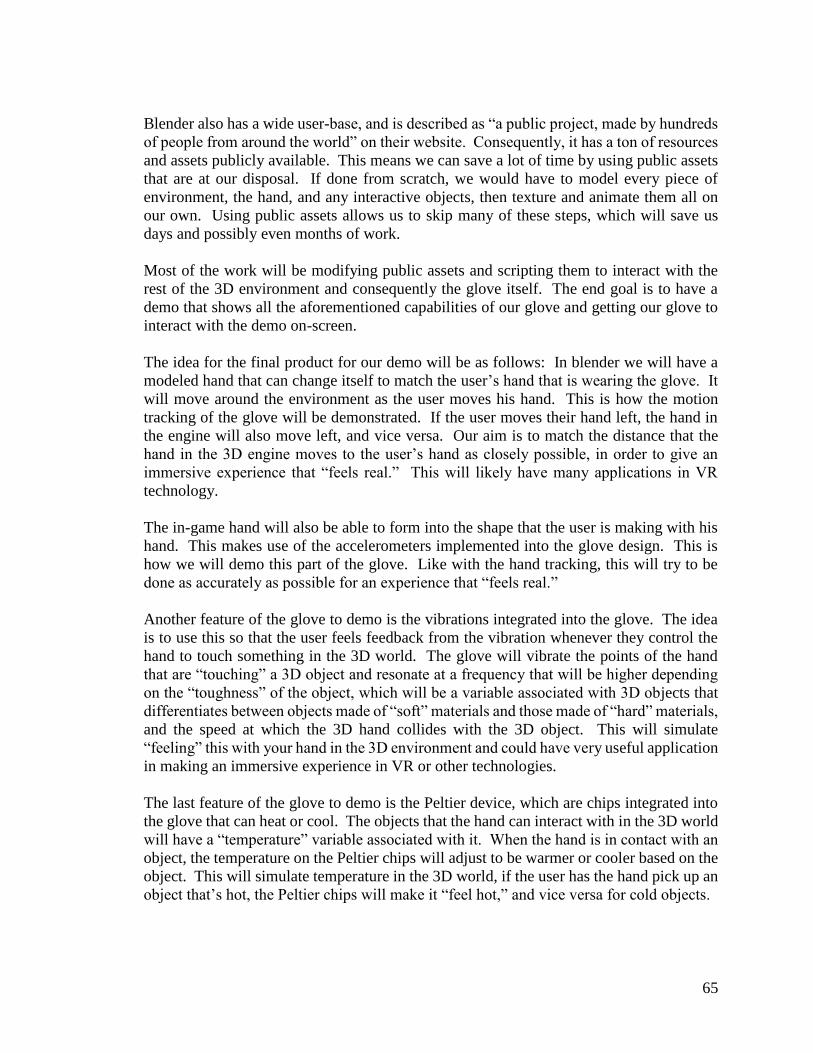
65
Blender also has a wide user-base, and is described as “a public project, made by hundreds
of people from around the world” on their website. Consequently, it has a ton of resources
and assets publicly available. This means we can save a lot of time by using public assets
that are at our disposal. If done from scratch, we would have to model every piece of
environment, the hand, and any interactive objects, then texture and animate them all on
our own. Using public assets allows us to skip many of these steps, which will save us
days and possibly even months of work.
Most of the work will be modifying public assets and scripting them to interact with the
rest of the 3D environment and consequently the glove itself. The end goal is to have a
demo that shows all the aforementioned capabilities of our glove and getting our glove to
interact with the demo on-screen.
The idea for the final product for our demo will be as follows: In blender we will have a
modeled hand that can change itself to match the user’s hand that is wearing the glove. It
will move around the environment as the user moves his hand. This is how the motion
tracking of the glove will be demonstrated. If the user moves their hand left, the hand in
the engine will also move left, and vice versa. Our aim is to match the distance that the
hand in the 3D engine moves to the user’s hand as closely possible, in order to give an
immersive experience that “feels real.” This will likely have many applications in VR
technology.
The in-game hand will also be able to form into the shape that the user is making with his
hand. This makes use of the accelerometers implemented into the glove design. This is
how we will demo this part of the glove. Like with the hand tracking, this will try to be
done as accurately as possible for an experience that “feels real.”
Another feature of the glove to demo is the vibrations integrated into the glove. The idea
is to use this so that the user feels feedback from the vibration whenever they control the
hand to touch something in the 3D world. The glove will vibrate the points of the hand
that are “touching” a 3D object and resonate at a frequency that will be higher depending
on the “toughness” of the object, which will be a variable associated with 3D objects that
differentiates between objects made of “soft” materials and those made of “hard” materials,
and the speed at which the 3D hand collides with the 3D object. This will simulate
“feeling” this with your hand in the 3D environment and could have very useful application
in making an immersive experience in VR or other technologies.
The last feature of the glove to demo is the Peltier device, which are chips integrated into
the glove that can heat or cool. The objects that the hand can interact with in the 3D world
will have a “temperature” variable associated with it. When the hand is in contact with an
object, the temperature on the Peltier chips will adjust to be warmer or cooler based on the
object. This will simulate temperature in the 3D world, if the user has the hand pick up an
object that’s hot, the Peltier chips will make it “feel hot,” and vice versa for cold objects.

66
To demonstrate all of this at the same time, the demo will have a table with multiple objects
that the glove can interact with. This will make demonstrating the features of our glove
much easier as we’ll be able to do it all at once in one sitting. There are multiple ways to
use these objects to demonstrate these features: A blue ball with a lower “temperature
value” and a red ball with a higher “temperature value” to show the Peltier devices, a “soft”
and “hard” ball that can demonstrate vibrations, or a “stove top” on the table with a field
that will warm the Peltier chips when the hand is in the field. This environment will have
to be created, modeled, textured, and scripted using blender.
We’ll start by creating a demo without the glove, so we can make sure physics and
interactivity works before we implement our device. We can start the making the demo by
creating the table, followed by making the ground, a block to place on top of the table to
test the physics, and a placeholder hand. Once these assets are implemented, we can script
the objects to react to gravity and collisions, make the hand controllable with the keyboard,
and position the camera and allow it to be controlled with the mouse. We will also need to
texture everything, so it looks more presentable, and possibly add a skybox as well to make
it more immersive.
Modeling & Object Creation Blender gives us many tools to help create the demo for our project. The first thing we do
is change the unit type in the scene tab to “Imperial.” This means the units will represent
feet and inches, which will be helpful for us because it helps correlate between lengths in
real life and lengths in the demo environment, and imperial units make the most sense for
this because they’re more common in United States. We want to do everything we can to
make the demo feel like a real application and keeping scaling consistent will help with
that.
The create tool allows us to make many basic shapes and objects, and we will use it to
make several basic objects for the demo. Now we’re going to make a table, which will
have many demo objects placed on top to help with our demonstration. This is done using
a series of cubes that we modify. The desktop is a cube transformed to be thin and wide,
while the legs are all cubes made to be tall and skinny. Then we position them together
and combine it with Ctrl-J to turn into one object and rename it to “table.”

67
Figure 45: Screenshot of Blender Interface
Figure 46: Table before legs were added

68
Figure 47: Table after legs were added
Now we need to add a ground. This is very simple, I just create a mesh with the same tool
I used to make the blocks and use the properties window to change its location to (0,0,0),
at the center of the 3D space, and increase the scaling on the x and y plane to make it large
enough to fit everything on.
Once we have that, we need to import a hand model. Modeling out a brand-new model is
time consuming, so importing a free one is ideal. free3d.com is a website that specializes
in royalty free assets, from which we can get a royalty free model to use for our project.
[20] The model we’ve imported is “Realistic Hand 3d model” from user
“mohammadalizadeh” on free3d.com.

69
Figure 48: Cover image of imported hand
Once downloaded, we simply use File -> Import -> 3d Studio (.3ds) and select the
downloaded file and the hand model is now in our program. The hand is a little too large,
so I use the properties window to scale it down to 0.1 on all axes and change the rotation
to have the fingers forward facing towards the table at start.
Figure 49: Completed table and plane with imported hand
We’ve also added a block above the table to test the physics and positioned the camera to
where it’ll need to be for the in-game vision.

70
Physics Implementation Adding the physics is actually very easy to do in blender. We change the “gravity” value
under the scene tab in the properties window to 32.2 ft/s2 to emulate real life. Now we use
the “physics” tab in the properties window, where we can change the physics type of each
of the objects. For the table and the block, we change the physics type from “static” to
“rigid body.” This causes these objects to be affected by gravity, so they’ll fall until they
collide with something else or the plane we’ve used as the ground. For the plane, we leave
the physics type as “static,” as we don’t want that to fall. The camera will also be left as
static so that it doesn’t move.
The hand will be controlled with the keyboard for now and later changed to be controlled
with the glove. We change the physics type for the hand to “dynamic” for this reason.
This leaves us with a problem, as the hand will now be affected by gravity, but we want to
be able to control it. There’s many ways around this issue, this will be addressed when we
script it.
With all this implemented, we can press “P” to start the engine and see that the block falls
and rests on the table, while the table rests on the ground. To make the collision box for
the block more accurate, we check the “collision bounds” box at the bottom of the physics
tab and change the bounds to “box.” This makes the collision bound of the object more
block-like.
Figure 50: Physics settings for the block
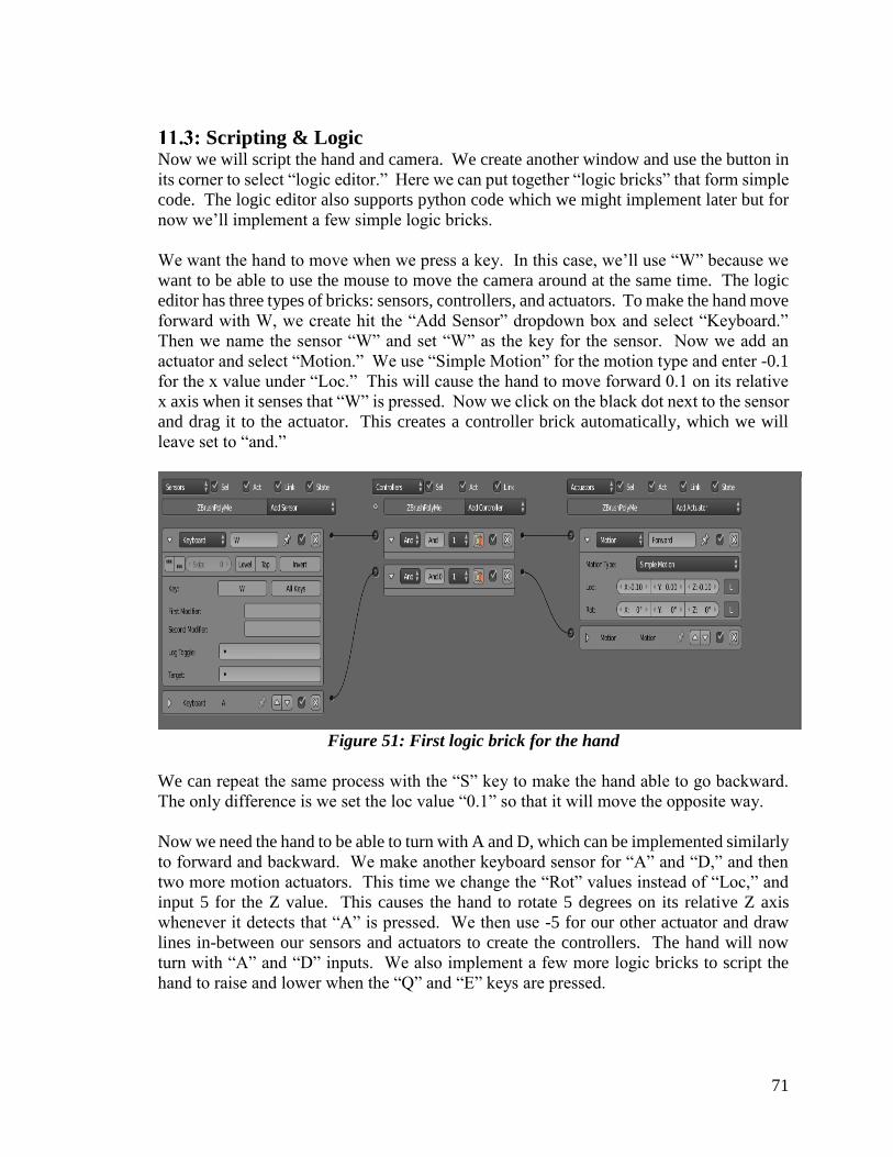
71
Scripting & Logic Now we will script the hand and camera. We create another window and use the button in
its corner to select “logic editor.” Here we can put together “logic bricks” that form simple
code. The logic editor also supports python code which we might implement later but for
now we’ll implement a few simple logic bricks.
We want the hand to move when we press a key. In this case, we’ll use “W” because we
want to be able to use the mouse to move the camera around at the same time. The logic
editor has three types of bricks: sensors, controllers, and actuators. To make the hand move
forward with W, we create hit the “Add Sensor” dropdown box and select “Keyboard.”
Then we name the sensor “W” and set “W” as the key for the sensor. Now we add an
actuator and select “Motion.” We use “Simple Motion” for the motion type and enter -0.1
for the x value under “Loc.” This will cause the hand to move forward 0.1 on its relative
x axis when it senses that “W” is pressed. Now we click on the black dot next to the sensor
and drag it to the actuator. This creates a controller brick automatically, which we will
leave set to “and.”
Figure 51: First logic brick for the hand
We can repeat the same process with the “S” key to make the hand able to go backward.
The only difference is we set the loc value “0.1” so that it will move the opposite way.
Now we need the hand to be able to turn with A and D, which can be implemented similarly
to forward and backward. We make another keyboard sensor for “A” and “D,” and then
two more motion actuators. This time we change the “Rot” values instead of “Loc,” and
input 5 for the Z value. This causes the hand to rotate 5 degrees on its relative Z axis
whenever it detects that “A” is pressed. We then use -5 for our other actuator and draw
lines in-between our sensors and actuators to create the controllers. The hand will now
turn with “A” and “D” inputs. We also implement a few more logic bricks to script the
hand to raise and lower when the “Q” and “E” keys are pressed.

72
There’s one more thing that needs to be scripted for the hand (at least for now). The hand
is set as a dynamic object and is thus affected by gravity, but we want to be able to control
the hand freely so it doesn’t drop to the ground as soon as the program starts. We make an
“always” sensor and another motion actuator. For this actuator we choose motion and give
it a force value in the Z direction. This force will always cancel out with the gravitational
force, so it produces the effect of the hand not being affected by gravity.
Figure 52: Full logic brick for the hand
Now the logic programming for our beta hand is complete. When we start the game engine
the hand can be moved with the keyboard and will collide with the block on the table and
knock it over. The only thing left for scripting is the camera.
Setting up the camera control is actually very simple; we select the camera and open up the
logic editor. We make a “Mouse” sensor and a “Mouse” actuator and connect them. Then
we set the Mouse actuator mode to “Look,” and it’s complete.
Figure 53: Camera logic brick
Now we can select “view” in the 3D viewport and select “camera.” When we start the
game engine, we’ll be looking through the camera, and can control it with the mouse.

73
Figure 54: Camera Viewpoint
11.4: Sound Effects
Another way to add immersion to the virtual reality experience is through sound effects.
The sound effects come from freesoundeffects.com, a royalty and license free website that
provides numerous sound clips for us to use. [21]
The following is an example: We give the cube a collision sensor to play the sound effect
of a can dropping. Now whenever the cube comes into collision with another object, the
“can_drop” sound will play. This gives the sphere a “hollow” feel to it, since it has an airy
tin sound upon impact.
Blender also has a built in “3D Sound” feature, which will make the direction of the sound
come from the direction of the object in the user’s headphones, which can be adjusted in
volume, gain, and distance limit however we want. This is especially important for a virtual
reality project, as being able to tell where the direction from which sound effects are
coming from is an important aspect of the immersive experience.
Figure 55 Sound Effect Implementation

74
Using this same scripting, we can implement sound effects on any objects, and script them
to be ongoing or one time, or add ambient music that always plays, giving our
demonstration one more layer of immersion.
11.5: Texturing Now we’ll add a few textures to our objects. This will help make our demo look much
more presentable. Our textures we'll come from the 3dtotal. This will give us royalty free
textures to use for our project. [22]
We can do this by opening up another window and changing it to the UV/Editor. Here we
can upload the textures we want to use. For now, we’ll apply three textures, one for the
table, one for the hand, and one for the plane.
Now we select an object and go to the “materials” tab in the properties window to create a
new material for the texture. From here we change the 3D viewport to “edit mode” and
start selecting objects that we need to texture. The edit mode allows us to be very specific
with how we want to apply textures, by letting us choose individual faces of each polygon
and choosing the texture and editing it individually for each segment, but for now we can
simply apply the texture to the entire object.
Here are the textures that we’ll be using for this prototype: The table has a wood texture
to make it look like a wood table, the plain has a grass texture to make it look like a grassy
terrain, and the hand has a skin texture to make it look like a human hand.
Figure 56: Grass texture

75
Figure 57: Wood and Skin Textures for the table and Hand
Figure 58: Skin Texture for the Hand
Once the selection is made we simply use the “unwrap” option to have the texture is fully
visible. We repeat this process for each texture we want to apply.

76
Figure 59: Texture editing in blender
One last thing we can do to make the prototype demo look more presentable is to change
the horizon color to more resemble a sky in the middle of the day. Once we put it all
together here’s what our prototype demo looks like:
Figure 60: Textured and colored prototype Environment

77
12: HTC Vive & Setup
Our product will be demonstrated with the HTC Vive. The glove doesn’t necessitate use
of any virtual reality headset, nor does it require use of virtual reality to function. That
being said, the idea for this project was made to be implemented with virtual reality, as it
can greatly enhance the current virtual reality experience. Because of this, we want to
demonstrate our device’s functionality in conjunction with virtual reality.
We chose the HTC Vive for our demonstration because it’s a high-quality headset that is
compatible with a lot of software due to SteamVR. It has a resolution of 1080 by 1200
pixels per eye, a 90Hz refresh rate, and a 110-degree wide field of view. It comes with two
base stations, also known as lighthouses, which make tracking possible in a room setup. It
also comes with two controllers, but this won’t be used for our demonstration.
Figure 61 HTC Vive with two lighthouses and controllers
The Vive also has a front camera and an audio jack installed. The audio jack will allow
sound effects incorporated into the demo to be heard.
SteamVR is compatible with most virtual reality hardware, from Google Cardboard to
Oculus Rift. It’s also royalty free with no licensing fees and no requirement for approval.
[23] This means that whatever we create will be compatible with almost any virtual reality

78
system and it won’t cost us anything to develop with. SteamVR is also one of the most
widely used virtual tracking systems today, so any virtual reality consumer will already be
familiar with it.
The Vive itself requires a little bit of setup to use. Its biggest feature is its room tracking
technology, which lets you walk around a room in virtual reality. This requires two
lighthouses on each corner of the room, which should be station 6 feet 6 inches off the
floor, in a 6 feet 6 inch by 5 feet clear area. It also requires a wired connection to the PC
because it needs a direct connection to the video card, as well as a USB connection and a
power connection. The PC will run the software, and the glove will be connected via
Bluetooth. The lighthouses require a power connection through the wall and communicate
wirelessly with the headset.
Once the setup is complete, our glove will be ready to perform with our demonstration
loaded up. The user can explore a 3D space in a 5 feet by 6.5 feet area and interact with
the environment using the glove.
Figure 62 Room setup with HTC Vive
13: Implementation of Virtual Reality One of the most important parts of our project demo is to incorporate a virtual reality
headset to show the strength our device can have when used in conjunction of a virtual
reality setting. The first step to doing this is, is to incorporate the use of a virtual reality
headset, in our case an HTC Vive, into blender.
There are many ways to do this, that work for many different sets of virtual reality
hardware. One of the simplest ways is to use a slightly modified version of the free open-
source blender addon “virtual reality viewport,” by dfelinto. [24]

79
This addon allows for virtual reality in the viewport of Blender, helpful for building things
in reference to the headset. More importantly, it allows us to attach cameras to the headset
position and display them on the HMD.
Figure 63: Blender displayed in Vive HMD
The head is tracked by the lighthouses, and the camera attaches to the location provided by
the SteamVR tracking. The “center” of the headset’s standing space will be set to be right
in front of the desk. From there, the user will be able to look around the desk and walk a
short distance around the desk.
The headset itself will be programmed as a reference point for the hand. The hand will be
calibrated to the headset, and then the position of the hand will be calculated as a distance
from the hand based on the head as an origin point. This makes the most sense because
the headset will represent where the user’s “viewpoint” is in real life.
The screenshot shows the display on the Vive HMD, being reproduced as a flat image.
With this set up we can include all the functionality of a VR headset, including tracking,
motion-sensing, and 3D image generation.
Skeleton Rigging and Animation
Since finger tracking is one of the most important features of the glove, arguably even the
most important, we’re going to need the hand in our demo to be able to represent that, and
to do that we’re going to need the fingers on the model itself to move in conjunction to the
glove’s finger movements. This is where rigging comes into play, where we create an
animation rig for the hand and script it to move according to inputs it receives.
The first step is to create an armature in blender. Then we can scale it down and start
incorporating it into our hand model.

80
Figure 64: Incorporating a skeleton into the hand
Wireframes are very helpful for this, because they allow us to see through the models and
see what we’re doing.
Once we have the first bone placed, we can use the extend tool in edit to create a network
of bones to animate the hand with.
Figure 65: wireframe and skeleton for index finger
Three bones are used for each finger to match the number in the human body as well as
make it match more consistently with our device. Each finger will be able to rotate on
three axes.

81
With a skeleton placed for one finger, we can now pair it with the mesh to make the finger
fully adjustable. Once the pairing is done, the mesh (and our hand) will move freely with
the animation rig.
Figure 66: Example of finder adjustability
Now that this is done with one finger, the process can be easily repeated and done for every
other finger. The thumb will be done a little differently because it only has two thumbs,
so it will have slightly different scaling and only two bones.
Figure 67: Animation rig compelte for hand
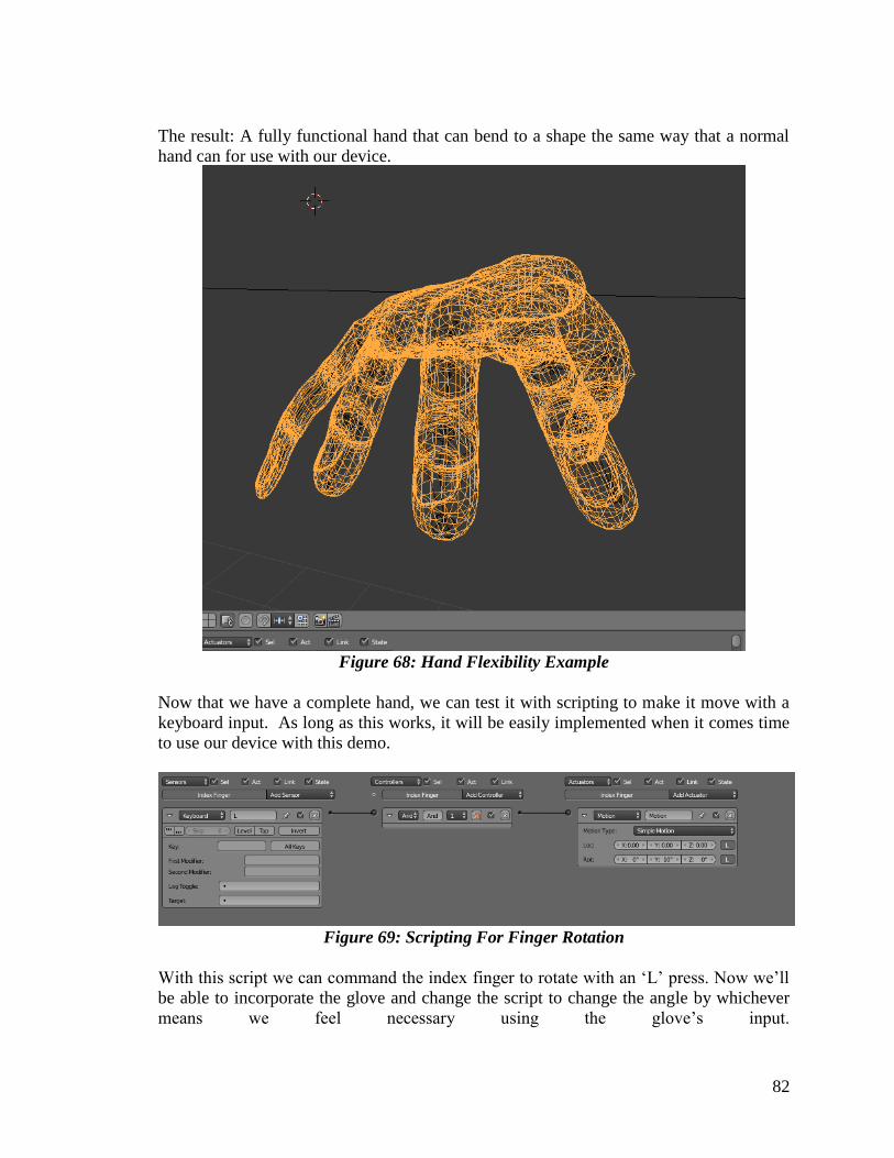
82
The result: A fully functional hand that can bend to a shape the same way that a normal
hand can for use with our device.
Figure 68: Hand Flexibility Example
Now that we have a complete hand, we can test it with scripting to make it move with a
keyboard input. As long as this works, it will be easily implemented when it comes time
to use our device with this demo.
Figure 69: Scripting For Finger Rotation
With this script we can command the index finger to rotate with an ‘L’ press. Now we’ll
be able to incorporate the glove and change the script to change the angle by whichever
means we feel necessary using the glove’s input.

83
14: Bringing it all together Now that we have the key features, let’s add a few things in that will make our demo ready
for our device. Keep in mind that the main things we need to demonstrate are: Motion,
haptic feedback (vibrations), and temperature change (Peltier devices). For this, we added
a few more objects to the desk.
Figure 70: More objects added to desk
The first of which is a sphere, which is added for two reasons. The first one is to be able
to demonstrate the haptic feedback of the glove more thoroughly. The glove is designed
to give haptic feedback at multiple “intensities,” so the sphere can simulate a “soft”
material while the block can simulate a “hard” material. The glove’s haptic feedback will
vibrate more intensely when coming in contact with the block than coming in contact with
the sphere.
The second reason is to demonstrate the positional aspect of the haptic feedback. A sphere
will be in contact at different points in your hand than a block when holding it. These
different points will vibrate to more simulate the “feeling” part of the project in a more
immersive way.
This will be done by adding an attribute to the objects that will be named “Mass” to each
object in the demo. This value will be used as a coefficient for the frequency of the haptic
feedback in the glove, which will also consider the velocity at which the glove collides
with the object. In physics, momentum transfer is based off of mass and velocity, so we’ll
have a function that takes the velocity of the hand coming into contact with the object and
multiplies it with the mass value of the object it comes into contact with. This can be
attributed to the object with the game properties tool as so.
84
Figure 71: Mass properties for sphere and cube
The other two objects added are thin cylinders on either side of the desk, one colored blue
and one colored red. This is a simple way to make “stove tops” that can be used to test the
Peltier portion of the glove’s functionality. The cylinders will be given a field of range,
extending upward but not out to the side. When the hand enters these fields, the Peltier
will heat or cool according to the color cylinder the hand is hovering above.
This can be accomplished by adding invisible, transparent, and taller cylinders on top of
the ones we have. This will be the “field” of the stovetops, and we can script a function to
begin when the hand comes into the space of these taller cylinders. This function will
instruct the glove to start heating up or cooling down the Peltier sensors, depending on
which cylinder the hand has entered.
Since we don’t want the Peltier devices to reach over certain temperatures, we’ll also script
it to check the current temperature of the glove on top of detection collision with the
invisible cylinders. This way the Peltier devices won’t overheat or get too cold.
15: Device Driver & Input In order for the device to communicate with the PC, a driver will be used. This driver is
what will interpret the signals that comes from the glove via the Bluetooth signal that will
be implemented. Blender will communicate with the driver to interact with the glove.
The device itself works in a differential system. Once the device is calibrated, the device
will send data on how it’s position changes over time. Because of this, the easiest way to
implement the device into Blender is to have it detect the driver as a game controller and
send inputs as the glove changes. Blender will take these inputs and adjust the in-game
hand accordingly.
For the finger movement, Blender will take ‘Axis’ inputs, where each segment of each
finger will have an ‘Axis’ event that the logic editor can keep track of. The axis will update
based on the inputs from the driver, and the finger poses will adjust accordingly, allowing
them to match the glove’s hand formation.

85
For the hand tracking, two ‘Axis’ inputs can be used. Each input from the driver will be a
different direction on the axis and based on that input the position of the hand will change
accordingly. The two axes will be used to separately control the hand on the XY plane and
the XZ plane, for full 3D movement.
Two more axes will be used for wrist tracking. The first axis will work similarly to the
finger, where it will change the angle the hand is at based on the user’s wrist angle. The
second axis will be used for wrist rotation, which will allow the user to turn their entire
hand on its side or upside down.
The Blender demo will also have to send data back to the driver for the haptic feedback
and Peltier device. Blender will send an ID for which vibrator or Peltier device on the
glove is being affected, and another value for the severity level. For the Peltier device the
severity value will tell the device if it needs to cool or heat up and how quickly it should
heat up. For the vibration, it’ll give a frequency for each device to resonate at.
For the axis sensors, Blender already has built in axis sensors and controller detectors,
making implementation for the hand movement easy to do. For the Peltier and haptic
feedback devices, the actuator in the logic section will invoke a python script to invoke
their effects.
Altogether the driver will be able to command the hand to move and adjust in the same
fashion that the glove does, and Blender will be able to command the driver to have the
glove Peltier devices change temperature and the haptic feedback devices vibrate at the
rate as scripted.
16: Python Scripting Blender allows for python scripting for more control on how the program works. This is
done through its python API which contains a large library of functions capable of math,
geometry, game logic, GPU functions, Audio Systems and more. [25] This is necessary
for how we want to implement the Peltier and haptic feedback devices on the glove.
The following code is attached as a controller to a Collision sensor on the object. When
the hand comes into collision with the object, it will use the getLinearVelocity() function
from the logic API and multiply it with the ‘Mass’ property applied to the object.
Figure 72 Python Haptic Feedback Code

86
This script will activate when the hand comes into collision with the object, then it will
calculate the difference between the hand’s velocity and the object velocity, multiply it by
the ‘Mass’ property, and pass it through the “glove.haptic” function.
The “glove.haptic” function is a function that will take a number and have the hand vibrate
by a frequency based on the number that passes through it. This function will be made to
interact with the driver to perform this functionality.
The Peltier function can be implemented in a very similar way using a collision detection
in the invisible cylinders on the table that serve as the “field” in which the glove will heat
up. Instead, it’ll use a function to calculate distance from the object and a base value for
the heat.
Figure 73 Python Script for Peltier Device
The distance is calculated by subtracting the hand position from the object position. This
distance is multiplied by the ‘Temp’ property associated with the cylinder and passed
through the function. The ‘Temp’ property on the red cylinder will be positive, and on the
blue cylinder will be negative, which the driver will interpret into instructions to warm or
cool the peltier device.
17: 3D Environment and VR Final
Blender’s logic scripting ended up not being used very much, as we ended up relying on
scripts a lot more for file I/O and events. Furthermore, VR addons for Blender have a way
to go in advancement. Addons were successful in using VR for the viewport, allowing VR
to be used while creating and modeling assets, but we’re not feasible to be used while
running the game engine. For this reason, we used the Unity game engine to implement
VR. Unity is a robust game engine that works well for VR projects and can import objects
from Blender easily. Python scripts were converted to C# code to fulfill all the same
functions, and the SteamVR plugin was used to incorporate VR.
Outside of that, the 3D Environment fulfilled all responsibilities. It was able to change in
response to input given from the configuration utility, and output back to the configuration
utility for feedback properly, all with VR working.

87
18: Configuration Utility The Configuration Utility provides a configurable interface between the hardware glove
and the 3D environment rendering software. The utility consists of two primary functions,
data passing and configuration management. Data passing handles data transmission
between the glove and the 3D environment. The glove passes the user’s hand motion to the
utility which forwards the data, so the 3D environment can update the position of the
corresponding virtual hand. The 3D environment passes touch and temperature data
through the utility which forwards the data to the glove to update the haptic and thermal
feedback experienced by the user. Configuration management allows for multiple
connected gloves to be mapped to their corresponding virtual counterparts. Each connected
glove is individually configurable to allow for customizing both the haptic and thermal
feedback intensity, along with pairing to identify which gloves represent the hands of
which user.
Development Overview The configuration utility will be developed utilizing Microsoft’s Visual Studio Community
2015 [26]. Visual Studio is Microsoft’s primary integrated development environment
which provides platforms such as the Windows API and Windows Forms. Team and code
management is supported along with full featured debugging. Visual Studio supports a
variety of programming languages including, but not limited to, C, C++, Visual Basic, C#,
Python, and JavaScript. The Community edition is a free version of Visual Studio with a
license that restricts use to individual or team development of open source projects. The
configuration utility was developed using the C# programming language and following
Microsoft’s C# and .NET coding standards.
Use Case Use case diagrams also known as behavior diagrams are used to describe a set of actions
or use cases that some system or systems should or can perform in collaboration with one
or more external users. Each use case provides an observable and valuable result that is
product of the action or actions taken by the user. When used to describe software, use case
diagrams can specify, external requirements of a system, functionally of a system that is
offered to a user, and the effect the system has on the environment.

88
Figure 74: Utility use case diagram
The use case diagram for the configuration utility is shown in the figure above. There are
three actors that interact with the utility. They are the user, the blender 3d software, and
the hardware glove. The diagram shows that from the glove and blender’s perspective, the
utility exits only as a gateway for transmitting and receiving data between them. This has
the effect of isolating the hardware glove and 3d software from each other allowing for
independent development and maintenance of each component. The primacy actor that
interacts with eh configuration utility is the user. From the use case diagram, the user uses
the utility to perform three major tasks each of which is supported by minor tasks. The
major tasks for the utility are managing profile, setting the mode of the utility, and
configuring connected glove devices.
Managing Profile is supported by the actions of creating, modifying, loading, and deleting
profiles. These actions are how the user manages the memory of the utility. Configurations
and profiles are stored in the utility directory using an xml scheme. When loaded, the
profiles preserve settings, so the user does not have to go through the process of configuring
the same glove every time the utility is started.
Setting the utility mode is how the user toggles a selected glove profile between regular
and debug modes. While in debug mode, this action is supported by three additional actions
that are only available while in debug mode. Real-Time view of feedback allows the user

89
to real-time updating charts of the outputs and inputs to all of the major electrical sensors
and actuations in the hardware system. The commanded and actual value of the vibration
motors and Peltier devices will be displayed. The real-time positional displacements of the
accelerometers will be displayed. Injecting of temperature and touch data allows the user
to send and observe signals to the vibration and Peltier devices. The debug mode aids the
user in assessing the functionality of the hardware and isolating potential faulty devices.
When the utility is in normal mode, the user can undertake profile management and
individual glove configuration. Synced gloves can have their parity set, be paired together,
and have the hardware limits for touch and temperature set. While in normal mode, the
utility will act as the data relay and transformer between the glove and the 3d software.
System Architecture The structure of the configuration utility consists of a graphical user interface layered on
top of data packager that converts a serial connection interface from a Bluetooth device
into a windows process interface connected to a 3D rendering software. In between the
user interface and the connection logic sits the profile manager, linear interpolator,
debugger, and the configuration storage. The Layout of the utility is shown in the figure
below.
Figure 75: Utility Architecture Diagram
The profile manager is the main component of the utility. It handles the creating and storage
of profiles, routing of data through the utility, responds to the user interface, and provides
the linear interpolator with the user specified limits for generating feedback signals in the
glove device.
The debugger is the primary means for accessing operational issues with a connected glove
device. The debugger sits directly between the user interface and the serial connection.
This configuration allows for isolating a glove device from the remain system. Through
the debugger, the user can monitor real-time feedback of glove motion, and the current
commanded vibration and temperature feedback. The debugger also provides the user with
an interface for injected feedback signals directly to individual feedback devices on the
glove, so the response can be monitored.

90
The role of the linear interpolator is to transform the touch and temperature values from
the virtual environment, into the corresponding feedback values using the limits set by the
configuration utility. Linear interpolation is the method of curve fitting using linear
polynomials to construct new data points within the range of a set of known data points.
Setting the high and low range for the touch and temperature feedback, allows the user to
scale the intensity of the feedback response as well as to ensure that the glove operates
within the limits imposed by the hardware.
Figure 76: Utility Class diagram
The class diagram above shows the preliminary design of the configuration utility software.
The configuration utility is broken down into several class. Each class provides a specific
service to the software. The use of the object-oriented design methodology allows for
software development that is streamlined, highly modular, and easy to update and maintain
such that additional future features can be readily implemented.
The heart of the software is the Util Core. The core provides the logical brain of the
software and is composed of other classes. The brain is responsible for updating the
graphical user interface, handling of software state, controlling inbound and outbound
communication, managing connected glove components, and controlling the interpolation

91
routines. The Utili Core is composed of four direct classes; process Comm, Interpolator,
Serial Comm, and Glove.
The glove class organizes and provides and interface for the configuration utility to
manipulate and interact with a connect glove. Each connected glove is represented
internally by an instance of the glove class. The glove class provides the methods needed
to manipulate the debug mode, pairing between gloves, as well as creating and removing
the glove. Each glove is composed of multiple electronic devices. Each of these devices is
represented by the Electric device class. Each class provides an interface for reading and
writing to the device. The physical location the electric device on the glove is also set so
that the virtual hand can be mapped one-to-one with the hardware glove.
Inter-Process Communication The Process Comm handles the data communication between the configuration utility
software, and the 3D environment software. The process comm establishes manages and
maintains the communication connection. To facilitate this, the process comm will use an
inter-process communication available on a windows system.
Inter-process communication refers specifically to the mechanisms an operating system
provides to allow the process to manage shard data. Typically, applications can use IPC in
a client-server scheme where the client request data and the server responds to clients. IPC
is divided into categories which vary based on software requirements, such as performance
and modularity requirements, and system circumstances, such as network bandwidth and
latency. There are several inter process communication schemes available on a windows
system. [27]
18.4.1: File
A file is a storage structure on a digital medium. A major portion of an operating system is
the file server which allows process to create, delete, modify, read, and write files. Process
can leverage this mechanism to provide rudimentary communication by reading and
writing to the same file. File communication is available on most operating systems.
18.4.2: Socket
Data sent over a network interface, either to a different process on the same computer or to
another computer on the network. Leverages the power of TCP and UDP protocols to
provide inter process communication and is available on most operating systems.
18.4.3: Unix domain socket
Similar to an internet socket but all communication occurs within the kernel. Domain
sockets use the file system as their address space. Processes reference a domain socket and
multiple processes can communicate with one socket. Available on windows with windows
10.
92
18.4.4: Message queue
Data stream similar to a socket but all communication occurs within the kernel. Domain
sockets use the file system as their address pace. Processes reference a domain socket and
multiple processes communicate with one socket. Available on windows.
18.4.5: Pipe
A unidirectional data channel. Data written to the write end of pipe is buffered by the
operating system until it is read from the red end of the pipe. Two-way data streams
between process can be achieved by creating two pipes utilizing standard input and output.
Available on windows.
18.4.6: Named pipe
Combination of File and Pipes, allows multiple process to communicate. Available on
windows.
18.4.7: Shared Memory
Multiple processes are given access to the same block of memory which creates a shared
buffer for the processes to communicate with eat other. Available on windows.
18.4.8: Message Passing
Allows multiple programs to communicate using message queues and/or non-OS managed
channels. Not OS dependent.
18.4.9: Memory-mapped file
A file mapped to RAM and can be modified by changing memory addresses directly
instead of outputting to a stream. Similar to the File method. Available on windows.
18.4.10: Selected Inter-Process Communication Scheme
The Process Comm will use the file communication method due to its simplicity of
implementation. The basic operations that can be performed on a file are; create, change
permissions, open, read, write, and close. In addition, files can be moved, modified, grown,
and shrunk. Process comm and the 3D environment software will communicate using two
predetermined files on the windows operating system. The files will be created at the
startup of the configuration utility and deleted when the utility is determined.
The first file is designated as the communication point for passing positional data that
utility received from the hardware glove to the 3D environment software in order to update
the position of the virtual hand. Blender will continuously monitor the file to determine if
new positional data is available. When available data is detected, Blender will retrieve the
next complete set of input data from the file. The configuration utility will receive updated
positional data from the hardware glove. After receiving the data, the utility maps, formats,
and writes the data to the file for Blender to retrieve. The file will be designated as a plain
text file and be named. “Util_to_Blender.txt”. The following figure shows the delineation
of the data written to and read from the file.

93
Figure 77: Util_to_Blender.txt
Each data set is framed by a start and end indicator. Next the glove id is given so that the
updated positional data can be applied to the correct virtual hand when multiple hardware
gloves are in use. The majority of the data set consists of the accelerometer data itself. This
data is calculated by the processor on the glove itself. Each line begins by identify the
accelerometer so that the data can be applied to the correct joint on the virtual hand. The
data on each line consists of the changes in all 6 degrees of freedom present in a three-
dimensional system. These are the changes in the three translational directions x, y, and z,
along with the changes in the three rotational directions, x-axis, y-axis, and z-axis. As each
data set is read by Blender, the data block is removed. As new data is received from the
glove, a new data block is added. This effect results in the transfer file continuously
growing and shrinking as both Blender and the configuration utility communicate.
The second file is designated as the communication point for passing touch and temperature
data from Blender to the configuration utility where it is processed and sent to the hardware
glove to drive the vibration and Peltier devices to produce the feedback response. The
configuration utility will continuously monitor the file to determine if new feedback data
is available. When available data is detected, the utility will retrieve the next complete set
of input data from the file. Blender will generate updated feedback data as a result of
updated positional data. After generating the data, Blender maps, formats, and writes the
data to the file for the utility to retrieve. The file will be designated as a plain text fiel and
be named “Blender_to_Util.txt”. The following figure shows the delineation of the data
written to and read from the file.

94
Figure 78: Blender_to_Util.txt
Each data set is framed by a start and end indicator. Next the glove id is given so that the
updated feedback data can be applied to the correct virtual hand when multiple hardware
gloves are in use. The majority of the data set consists of the feedback data itself. This data
is produced by Blender as a result of the updated position of the virtual hand within the 3D
environment. The data section of each frame is split into two parts. The first part consists
of a line of data for each of the Peltier devices on the hardware glove and corresponds to a
temperature measurement point on the virtual hand. Each line begins by identifying the
temperature measurement point so that the data can be applied to the correct Peltier device
on the hardware glove. The data on each line consists of the currently measured
temperature of that point in the 3D environment. The second part of the data section
consists of a line of data for each of the vibrational motors on the hardware glove and
corresponds to touch force measurement point on the virtual hand. Each line begins by
identifying the touch force measurement point so that the data can be applied to the correct
vibrational motor on the hardware glove. The data on each line consist of the currently
measured force applied to that point in the 3D environment. As each data set is read by the
configuration utility, the data block is removed. As new data is generated by Blender, a
new data block is added. This effect results in the transfer file continuously growing and
shrinking as both Blender and the configuration utility communicate.

95
Bluetooth communication The serial comm class, handles the communication between the utility software and the
glove itself. The communication protocol that will be used is Bluetooth. Bluetooth is an
industry-standard protocol that enables wireless connectivity for a multitude of devices.
The key features that make Bluetooth the go to protocol from a software perspective, are
its presence in virtually all modern PCs, its support in modern operating systems, it is a
standardized technology with a multitude of resources, and it is a well-defined and familiar
programming interface that allows for quick development.
Bluetooth on windows provides functionality with similarity to TCP. [28] Using Bluetooth
in a standard networking implementation, results in Bluetooth connectivity and data
transfers being programmed through windows sockets function calls. This approach
combines common windows sockets programming techniques and principles with specific
Bluetooth extensions. In addition, Bluetooth provides features such as discovery and
notifications which a necessary for any communication scheme operating in a wireless
environment. Support for Bluetooth on Windows Operating Systems began with Windows
XP Service Pack 1 and includes all subsequent releases of the Windows Operating System.
Microsoft provides two approaches for programming and using Bluetooth on Windows
devices; Using the Windows Sockets interface [29] or Managing devices directly by using
non-socket Bluetooth interfaces.
18.5.1: Selected Windows Bluetooth Method
[30]The serial comm will leverage windows provide Bluetooth APIs to establish a serial
UART connection. The serial comm provides methods to access the serial connection and
read the input message from the hardware glove and provide an output message to the
hardware glove. The selected Bluetooth programming approach is the Windows Sockets
interface. As stated, this method extends the windows sockets API with Bluetooth standard
features. Windows Sockets enables programmers to create applications that transmit data
across the wire in a manner that is independent of the network protocol being used. The
Winsock API provides access to advanced networking features such as multicast and
Quality of Service.
Bluetooth is a serial communication protocol that operates using packets that consist of
headers and administrative fields surrounding a payload of data. The nature of the
configuration utility will leverage the structure of the connection to utilize the headers and
administrative information to identify both the source and recipient of transmitted data.
The payload can then be reserved for the actual data being transmitted. The configuration
utility uses Bluetooth for communication in two directions.
The first direction is receiving data from the hardware glove. When communicating in this
direction, the utility will receive updated positional data from the hardware glove. This
data consists of the changes in all 6 degrees of freedom present in a three-dimensional
system. These are the changes in the three translational directions x, y, and z, along with
the changes in the three rotational directions, x-axis, y-axis, and z-axis. Each set of 6 degree
of freedom changes also contains the identity of the generating accelerometer When
receiving the data. The utility identifies the source glove and then maps and formats the

96
data so that the updated positional information can be transmitted to Blender using the file
inter-process communication scheme.
The second direction of communication is sending data from the utility to the hardware
glove. First the utility processes the feedback data received from Blender. Interpolation is
used to both scale and determine the driving signals necessary for the feedback devices.
These signals are then sent using Bluetooth to the hardware glove. The Bluetooth module
on the glove itself, identifies the data meant for it form the header and administrative
information in the Bluetooth packet. The payload of the packet contains the device driving
signal, along with Identifies for which Peltier or vibrational device that signal is for.
Interpolation The interpolator class contains the mathematical logic for converting the blender
environment response into the signal values needed to drive the electrical devices on the
hardware glove. The first action the interpolator does is scale the signal value so that it falls
in-between the associated limits for the glove. Each Peltier and vibrational device contain
documented values that correlate input signal value to output value. If an output signal
value that is not provide is need, then interpolation must be used to construct the necessary
output signal value. Interpolation is a method of constructing new data points within the
range of a discrete set of known data points. There are a variety of interpolation methods.
[31]
18.6.1: Piecewise constant interpolation
This is the simplest method of interpolation. If a need data point falls between two known
points, the value of the of the closest known point is chosen and assigned to the data point.
This method is fast and simple to implement.
18.6.2: Linear interpolation
This method treats the space between known data points as lines. If a need data point falls
in-between two known points, the value is determined by a liner equation and governed by
the two known points on either side if the needed point. Like piecewise interpolation, linear
interpolation is fast and simple to implement while providing increased accuracy.
18.6.3: Polynomial interpolation
This method is an extension of liner interpolation. While linear interpolation is of degree
one, polynomial interpolation can take the form of any degree greater than one. It is
guaranteed that a polynomial can be found that contains the known data points however,
the region between that data points may not be an accurate representation of the needed
behavior characteristic of the device. This method is slower than the previous two and
much more difficult to implement as the degree of the polynomial increases.
18.6.4: Spline interpolation
This method is a variation of linear interpolation. Instead of connecting the known data
points with straight lines, individual low degree polynomials are used such that a smooth

97
curve that passes through the known data points is produced. Spline interpolation can
produce more accurate results than other methods but is much more difficult to implement.
18.6.5: Selected Interpolation Method
Linear interpolation is the method that will be used by the interpolator class. The electric
devices operate on small signal ranges. It is the noticeability of an output difference rather
than the precise accurate value of the output that is most important to the design. The figure
below shows how linear interpolation will be used to drive the output signal for the
electrical feedback devices.
Figure 79: Linear interpolation example [32]
In the figure, the x axis represents the commanded feedback value, touch or temperature,
from the 3D environment. The y axis represents the output signal needed to drive the
corresponding feedback device to the required value. The points (x1, y1) and (x0, y0)
represent the set configuration limit for the feedback signal. The value x is the current value
commanded by the 3D environment. First the value is scaled to fall in-between the
configuration limits. Next the equation below is used to linearly interpolate and find the
output signal value y. This is the signal that is passed to the hardware to drive the
corresponding electrical device to produce the desired feedback experience.
Equation 3: Liner Interpolation [33]
System Deployment The configuration utility will be developed for and deployed on a Windows 10 machine.
The Windows Operation system was chosen because it is the most common and most
utilized computer operating system in use today. It is also designed to be user friendly and
the visual studio development environment is specifically designed to work on and interact
with the Windows operation system. The configuration tool system foot-print and
deployment plan are shown in the figure below.

98
Figure 80: Utility Deployment
The root directory will contain the compiled utility executable along with a configuration
xml file and subdirectories for profiles and system resources. The resources directory will
contain subdirectors for images and sounds. These images and sounds are those utilized by
the utility itself i.e. the splash screen, button sounds etc.
The profiles directory contains the stored profiles in xml form. Each profile contains the
configuration settings for one or more glove devices. These settings consist of Bluetooth
I.D. for the glove, parity of the glove (left or right hand), pairing of gloves to represent a
single user, and the interpolation limits for temperature and touch feedback.
Data Design The data design of the System consists of three parts. The input/output design details how
data enters and leaves the configuration utility. The internal design details how data is
manipulated and routed within the utility. The storage design details how persistent data is
stored and accessed by the utility.
The input/output data design is centered around serial-based message passing. Serial
messaging is characterized by individual 8bit characters transmitted 1-bit at a time between
two components. Serial messaging is simple, relatively easy to implement and is the
standard scheme use by many commercial devices such as USB and Bluetooth.

99
The internal data design consists of how data is manipulated inside the utility. The utility
will be develop using the object-oriented programming paradigm. In object-oriented
programming, data is associated with objects. Objects contain the data and provide
methods so that other objects can manipulated the data. The utility, data is associated with
a particular glove object. Input signals from the glove is mapped to the corresponding glove
instance in the utility. The utility the packages the data so that blender can associate a set
of data with the corresponding virtual representation of the manipulated hand.
The storage data design determines how persistent data is maintained between uses of the
utility. To accomplish this, the XML data structure will be used. XML, Extensible Markup
Language, is a markup language that defines a set of rules for encoding documents in a
format that is both human-readable and machine-readable. The design goals of XML
emphasize simplicity, generality, and usability. XML is defined through the use of a
Schema. The schema detals what a valid entry into the XML must contain, along with what
a valid entry can contain. Using XML, system configuration settings and glove profile can
make use of individual defined schema to create, modify, and store their states in XML
format in the utility directory. XML is stored the form of a file, and as a file, it is subject
to all the standard operations available to file manipulation.
User Interface Design The user Interface utilizes the Windows Forms API to present a simple user-friendly
environment for accessing all the features of the configuration utility. The UI layout is
broken down into several distinct components detailed in the following sections.
• Splash Screen • Initial utility loading graphic
• Home Screen • Load, Create, Modify profiles • Add, Remove, Modify glove devices
• Configuration View • Modify feedback parameters for selected glove • Select left or right parity • Pair Gloves together
• Debug Screen • Display data received from the selected glove • Pass data to selected glove
18.9.1: Splash Screen
The Splash Screen is the initial entry point of the configuration utility. It serves to display
the Project Logo along with addition relevant information. The splash screen is shown in
the figure below.

100
Figure 81: Splash Screen
Some of the information displayed are for example; the project members, configuration
utility version, and copyrights. The functional use of the Splash Screen is to show that
configuration utility has successfully loaded and is starting up. A successful startup
transitions the configuration utility to the Home Screen.
18.9.2: Home Screen
The Home Screen is the primary user view for the utility and consists of three sections;
Menu Bar, Main Display, and Selection Tabs.
Figure 82: Home Screen

101
The menu bar is the primary administrative interface for the user and is where the high-
level functions of the utility are accessed. The actions provided by the menu bar are;
minimize, maximize, exit, create profile, load profile, close profile, and delete profile. Each
of the actions are detailed in the table below.
Action Description
Create Profile Creates a new profile for storing a set of glove configurations
Close Profile Closes the currently loaded configuration profile
Delete Profile Permanently deletes a configuration profile
Load Profile Loads a saved configuration profile
Minimize Standard windows action, collapses configuration utility to the
taskbar.
Maximize Standard windows action, fills display with the configuration utility
Exit Standard windows action, safely terminates the configuration
utility
Table 21: Menu Bar commands
The selection tabs are populated whenever a selected profile has saved configuration data
for a glove device. Each tab represents the data for a single glove that is associated with
that profile. Selecting a tab, updates the main display to show the configuration interface
for that glove. Closing a tab removes that glove from the display and erases the
corresponding configuration data from the saved profile.
18.9.3: Configuration View
Selecting a configuration tab from the home screen, loads the configuration view for that
glove device. The figure below shows the layout of the configuration view.
Figure 83: Configuration Tab

102
The configuration view is where glove devices are modified. The parameters available are;
hand parity, glove pairing, and the touch and temperature high low limits. Hand parity
designates whether the glove is left or right handed. This is used for interfacing with the
3D environment software, and for pairing of gloves. Selecting a parity is accomplished by
selecting the corresponding radio button. Glove pairing is the action of assigning two
gloves to represent both hands of a single user. Like parity, this is used for interfacing with
the 3D environment. It also allows for configuration settings to be mirrored across both
gloves. To pair two gloves, open the dropdown list in the entry field. The list will be
automatically populated with gloves that are part of the currently loaded profile, are of
opposite parity, and that are not currently paired.
The touch and temperature high and low limits are used to set the values used by the linear
interpolator when converting 3D environment values into glove signals. Setting these
values allows the user to tune the intensity of the feedback responses, as well as ensure that
hardware limits are not exceeded.
The displayed hand graphic will reflect the selected parity of the glove, the connection I.D.
of the glove, as well as display the number and location of sensors and feedback devices
the glove provides.
The debug option places the utility and glove into debug mode and loads the debug screen
for the selected glove. Debug mode allows for direct monitoring of glove state and
interaction with glove feedback devices.
18.9.4: Debug Screen
Debug mode is the primary method for assessing issues with the glove connection and/or
the glove itself. It is also used to test feedback response to aid in determining the best touch
and temperature limit settings for the user. Selecting yes on the debug menu on the
configuration view transitions the main display into the debug view shown in the figure
below.

103
Figure 84: Debut View
While in debug mode, the glove is disconnected from the 3D environment software. A
direct connection is established between the configuration utility and the glove hardware
providing access to the individual devices of the glove itself. The debug view provides two
features to the user, real-time display, and signal injection.
The primary feature of the debug view is the real-time display. Three charts that monitor
the accelerometer, touch, and temperature signals are displayed and updated in real-time.
Each of the charts displays data for every device of the corresponding type that the glove
provides.
The second feature of the debug view is the ability to inject touch and temperature feedback
signals directly to the glove. This is done one device at a time, and when used in
conjunction with the real-time display, provides a rapid interface for assessing technical
problems with the glove and identify potentially flawed or failed devices.
To exit the debug view, select the corresponding radio button on the debug menu. This
returns the user to the configuration view for that glove and resumes normal operation of
the glove.
Configuration Utility Final The final design of the configuration utility consisted of minor changes to the deployment
system scheme, and major changes to the user interface. Instead of using xml files, all
profile and file I/O communication files use plain text and are sorted with a custom
extension of “mitts” as opposed to “.txt”. The changes in deployment of the utility
consisted of a single root directory containing the executable and I/O files. The only
subdirectory is for the storage of glove profiles.
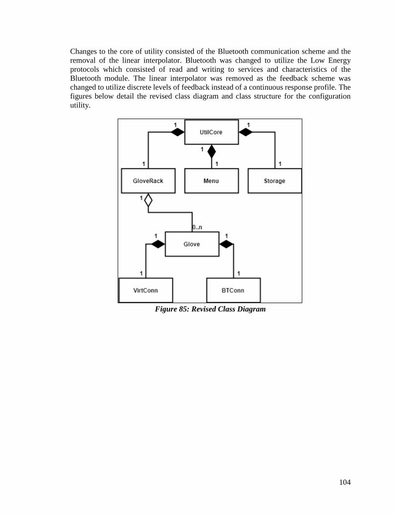
104
Changes to the core of utility consisted of the Bluetooth communication scheme and the
removal of the linear interpolator. Bluetooth was changed to utilize the Low Energy
protocols which consisted of read and writing to services and characteristics of the
Bluetooth module. The linear interpolator was removed as the feedback scheme was
changed to utilize discrete levels of feedback instead of a continuous response profile. The
figures below detail the revised class diagram and class structure for the configuration
utility.
Figure 85: Revised Class Diagram

105
Figure 86: Revised Class Structure
The use interface underwent the largest change. Design was switched from that of a full
graphical interface, to instead a console-based ASCII interface. The interface still provided
all the functionality of the original design. This changed occurred do to time constraints,
complexity with the original design, and a shift in focus to more critical areas of the system.
The figure below details the layout of the revised system.
Figure 87: Configuration Utility ASCII Interface

106
19: Testing Testing of the system will be conducted in three phases. Phase I consists of unit testing.
Each component will be tested in a standalone capacity. Phase II consists of integration
testing. Each components interface will be tested with the components it interacts with.
Phase III consists of a system testing. A fully integrated system consisting of all the
components will be tested to verify the completed system.
To facilitate early testing; stubs and drivers will be developed to simulate critical software
components, while breadboards and Arduino micro controllers will be used to test
individual hardware components. Stubs and drivers are pieces of code used to stand in for
some other functionality and act to simulate the behavior of an existing component or a
yet-to-be developed component. A driver will be developed to simulate the interaction
between the configuration utility and the 3D environment software. The driver will be
capable of receiving positional data from the utility and transmitting touch and temperature
data back to the utility. A stub will be developed and used to simulate the interaction
between the configuration utility and the hardware glove. The stub will transmit positional
data to the utility and receive touch and temperature data back from the utility. An Arduino
micro controller allows for testing of the individual glove components while the processor
circuity is still under development. Breadboards allow for connecting and testing hardware
components while the final PCB design is being refined, manufactured and delivered.
Phase I Phase I consists of unit testing [34]. Each individual component and device will be tested
in a standalone environment. A full test of the individual component functionality will be
executed. A stub and driver will be used to simulate the interaction between the
configuration utility and the hardware glove and 3D environment software. An Arduino
micro controller and breadboard circuit will allow for the testing of the individual touch
and thermal sensors, vibration motors, and accelerometers. Testing will cover all aspects
of the system and is broken down into two categories; software testing and hardware
testing. Software testing evaluates the software components functionality. A Stub will be
used to simulate the presence of a glove, and a driver will be used to simulate the 3D
environment software. Hardware testing evaluates the hardware components functionality.
An Arduino microcontroller and breadboard will be used to test individual hardware
components.
Phase II Phase II consists of integration testing [35]. The interface between sub components of the
system will be tested in a bottom up approach. Bottom-up testing is an approach where the
lowest level components are tested first. As components are test, they are used to facilitate
the testing of higher components. This is repeated until the upper most component in the
system hierarchy is tested. At each stage of the testing, software stubs and drivers, and
Arduino microcontrollers will be used to provide functionality for missing components.
Testing focused on the interface and data transmission between the components.

107
Phase III Phase III consists of system testing [36]. The completed system will be tested both software
and hardware components. Testing focused on full function the complete interface and data
transmission chain proceeding from glove to utility to 3D software, and the reverse. The
tests demonstrated continuity between all components of the completed system. Testing
will be performed and verified against the documented requirements specifications in order
to determine the final pass or fail status of the system.
Testing Management [37]Testing management outline and document the tests that are needed to demonstrate
compliance with the requirements specifications. The tests represent testing conducted
during all three phases of the testing process. Test management consists of two parts. The
First is test tracking. Testing is tracked through a Testing Traceability Matrix show in the
table below. A traceability matrix is a data structure used to assist in determining the
completeness of a relationship by correlating any two baselined documents using a many-
to-many relationship comparison. The testing matrix Identifies what test was performed,
when it was performed, who is responsible for performing the test, and the outcome of the
test.
Test ID Test Name Tester Test Result
(Pass/Fail) Test Date
1 Peltier Chris Fail 7/24/18
2 Vibration Motor Chris Pass 7/24/18
3 IC Sequencer Chris Removed
4 Accelerometer Chris Pass 8/15/18
5 Power Regulator Chris Pass 9/1/18
6 Thermistor Chris Removed
7 Digital Potentiometer Chris Pass 7/24/18
8 Battery Charger Chris Pass 10/5/18
9 H-Bridge Chris Pass 8/20/18
10 Peltier Controller Chris Pass 8/20/18
11 Motor Controller Chris Pass 7/24/18
12 Configuration Utility Francisco Pass 11/20/18
13 Windows Function Francisco Pass 11/4/18
14 Profile Manipulation Francisco Pass 11/6/18
15 Configuration
Manipulation Francisco Pass 11/6/18
16 Data receive Francisco Pass 11/8/18
17 Data Transmit Francisco Pass 11/8/18
18 Debugger Francisco Pass 11/15/18
19 SWD Chris Pass 10/8/18
20 LED Function David Pass 11/20/18
21 Data Format David Pass 11/22/18
22 I2C Read David Pass 11/25/18
23 Boot-Up Process David Fail 11/26/18

108
24 Blender Collision &
Physics Hunter Pass 11/1/18
25 Blender-Driver
Communication Hunter Pass 11/10/18
26 Hand Tracking Script Hunter Pass 10/15/18
27 Bluetooth Chris Pass 9/5/18
Table 22: Testing Traceability Matrix
Testing Procedures The second part of test management are the testing procedures. Each test outlined in the
traceability matrix has an associated testing procedure. Testing procedures detail how a test
is to be performed. Elements of a testing procedure indicate the test to be performed, who
is to perform the test, the procedure for performing and the equipment needed to perform
the test, and the pass/fail conditions for the test.
1: Peltier Test
• Description: Peltier devices must change temperature with respect to an applied current.
• Procedure: The Peltier devices will be individually connected to a current supply. The
current will be manually varied, and the produced temperature measured with a digital
thermometer. The current and the temperature shall be recorded along with any insights
into how the operation of the Peltier will interact with human skin and perception. Note
must be taken of the range of currents that the human hand, in the location designated for
the Peltier, is capable of sensing before the temperature becomes uncomfortable for the
user.
• Pass/Fail: To pass this test each, Peltier deice must demonstrate a heating and cooling
range of 40 degrees Celsius to 10 degrees Celsius.
• Who: Test will be performed by Chris.
2: Vibration Motor Test
• Description: Vibration motor devices must vary vibration frequency with respect to an
applied voltage.
• Procedure: The vibration motors will be individually connected to a voltage source. The
voltage will be manually varied, and the produced vibrational frequency will be measured.
The voltage and relative vibrational intensity shall be recorded along with any insights into
how the operation of the motor will interact with human fingertips and perception. Note
must be taken of the range of voltages where the human hand can perceive the vibration
magnitude and frequency of the motor.
• Pass/Fail: To pass this test, each vibration motor must demonstrate a vibration range that
can be perceived by the human hand as having a distinct difference from in vibrational
magnitude from the lowest setting to the highest setting.
• Who: Test will be performed by Chris.

109
3: IC Sequencer Test
• Description: IC sequencer devices must deliver a voltage after a specified time delay.
• Procedure: The IC sequencers will be connected to a digital multi meter. A timer will
be used, and the voltage output observed while varying the controlling capacitor. The
capacitor will be chosen such that the timer will give a multi second delay. This long delay
will only be used for testing purposes since the test technician is incapable of perceiving
micro second time differences.
• Pass/Fail: To pass this test, each IC sequencer device must demonstrate a delay in
voltage delivery with respect to controlling capacitor.
• Who: Test will be performed by Chris.
4: Accelerometer Test
• Description: Accelerometer devices must respond to changes in orientation and position
with respect to a normalized start point.
• Procedure: The accelerometers will be tested by connecting them to an Arduino board
through an I2C connection. The accelerometer will then be oriented, and the output data
passed to the Arduino which must be able to calculate the distance traveled by the device
from the acceleration data.
• Pass/Fail: To pass this test, each accelerometer must demonstrate and discriminate
between three degrees of freedom at a resolution of 14 bits.
• Who: Test will be performed by Chris.
5: Power Regulator
• Description: The power regulator must produce 3.3 volts using the schematic referenced
in the Power Regulator section.
Procedure: The power regulator must be prototyped on a breadboard, prototype board, a
custom PCB, or a combination of the three. After prototyping the input of the circuit will
be hooked to a bench top voltage source set to between 4.2 and 3.7 volts. The load of the
power regulator will initially be a 1 MΩ resistor to simulate a low current environment.
The voltage across this resistor will be checked with a digital multimeter. The load will
then be lowered to 1.1 Ω to simulate a high current environment. The voltage will be
checked with a digital multimeter.
• Pass/Fail: To pass this test the circuit must be able to maintain voltage on a load ranging
1 MΩ to 1.1 Ω. The 1.1 Ω resistor must be a high watt model.
• Who: Test will be performed by Chris.
6: Thermistor
• Description: The thermistor must vary its resistance in accordance to the equation and
design referenced in the Thermistor section.
• Procedure: The voltage divider will be implemented and the voltage at various
thermistor temperatures will be read with a multimeter.
• Pass/Fail: To pass this test the circuit must be able to vary its voltage with the
temperature on the thermistor.
• Who: Test will be performed by Chris.

110
7: Digital Potentiometer
• Description: The digital potentiometer must respond to I2C commands to change its
resistance.
• Procedure: The digital potentiometer will be connected to a voltage divider. The voltage
divider will be powered by a benchtop voltage supply. The circuit will be prototyped on
breadboard, prototype board, or a custom PCB. The digital potentiometer’s resistance will
be varied using the I2C controls on the I2C line. The output of the voltage divider will be
measured with a digital multimeter.
• Pass/Fail: To pass this test the circuit must be able to vary the voltage measured by the
digital multimeter in a fashion that can be controlled via I2C.
• Who: Test will be performed by Chris.
8: Battery Charger
• Description: The battery charger will be purchased from a supplier and must be verified
for quality before being used on the main PCB board. This is to ensure that the battery
charger does not over charge the lithium ion batteries or damage them from over current.
• Procedure: The charger will be plugged in and a digital multimeter will be used to check
the voltage across the leads. This must be less than 4.2 volts. The maximum current of the
charger must be checked using a digital multimeter. This current cannot exceed the stated
maximum current listed in the data sheet.
• Pass/Fail: To pass this test the battery charger must be able to charge the batteries to 4
volts and not exceed its posted current limit.
• Who: Test will be performed by Chris.
9: H-Bridge
• Description: The H-bridge must respond to the Enable/Phase design referenced in the
H-bridge section. It must be able to produce variable voltage based on the analog voltage
applied to the input terminals and change the polarity of the output voltage based on the
phase activation.
• Procedure: The circuit must be build using breadboard, prototype board, a custom PCB,
or a combination of the three. Power will be supplied with a benchtop voltage supply. The
input voltage and phase activation will be supplied by a voltage source while the output
will be measured by a multimeter.
• Pass/Fail: To pass this test the circuit must be able to generate varied voltages based
upon the input voltage and the phase of the voltage must be able to be changed upon
activation of the phase control circuitry.
• Who: Test will be performed by Chris.
10: Peltier Controller
• Description: The Peltier controller circuitry must be able to apply properly controlled
voltage across the Peltier device to generate the proper current that will drive the Peltier
device to the proper temperature. Since this is an integration test the circuit must contain
the H-bridge circuitry as well as the circuitry for the I2C controlled digital potentiometer
circuitry.

111
• Procedure: The Peltier controller test will implement the Peltier controller schematic
referenced in the Peltier Controller section. It will include the H-bridge circuity. The circuit
must be build using breadboard, prototype board, a custom PCB, or a combination of the
three. Power will be supplied with a benchtop voltage supply. This circuit must implement
a digital potentiometer which should be controlled via I2C. Temperature must be measured
using a digital thermometer such as the built in one on many digital multimeters.
• Pass/Fail: To pass this test the Peltier controller must be able to vary temperature in both
the positive and negative direction. It must be I2C and GPIO controlled with the I2C
controlling the magnitude of the temperature change and the GPIO pin controlling the
direction.
• Who: Test will be performed by Chris.
11: Motor Controller
• Description: The motor controller circuitry must be able to apply properly controlled
voltage across the motor to generate the proper vibrational frequency and magnitude. Since
this is an integration test the circuitry must incorporate an I2C controlled digital
potentiometer circuitry.
• Procedure: The motor controller test will implement the Motor Controller schematic
referenced in the Motor Controller section. The circuit must be build using breadboard,
prototype board, a custom PCB, or a combination of the three. Power will be supplied with
a benchtop voltage supply. Vibrations of the motor should be varied by application of I2C
controls.
• Pass/Fail: To pass this test the circuit must be able to vary the frequency of vibration in
the vibrational motors. It must be controlled by I2C with the I2C potentiometer controlling
the frequency of vibration.
• Who: Test will be performed by Chris.
12: Configuration Utility
• Description: The Configuration Utility must be able to be installed and initiated on the
operating machine.
• Procedure: The configuration utility is placed onto the operating machine as detailed in
the system deployment section of this document. The machine must be using the Windows
10 operating system. The configuration Utility is initiated by double clicking the
“MITTSutility.exe” executable in the root directory.
• Pass/Fail: The splash screen should appear followed by the Home screen. The utility
must not freeze or crash.
• Who: Test will be performed by Francisco.
13: Windows Function:
• Description: The standard windows application functions of minimize, maximize, and
close are tested.
• Procedure: The configuration Utility is first initiated by double clicking the
“MITTSutility.exe” executable in the root directory. The minimize windows button is
selected from the top right corner of the utility home screen. The utility is collapsed to the
task bar. The minimized utility is selected on the taskbar and restored to its original state.
The maximize button is selected from the top right corner of the utility home screen. The

112
utility fills the display. The maximize button is selected from the top right corner of the
utility home screen. The Utility returns to its original state. The close button is selected
from the top right corner of the utility home screen. The utility process is terminated, and
the utility is closed.
• Pass/Fail: The minimize, maximize, and close buttons should correctly function with
respect to a standard windows application. The windows functions must not crash the
utility or alter any of its parameters.
• Who: Test will be performed by Francisco.
14: Profile manipulation
• Description: The profile manipulation operations of the configuration utility are tested.
• Procedure: The configuration Utility is first initiated by double clicking the
“MITTSutility.exe”. The create profile option is selected from the menu on the home
screen. A name is given to the new profile, the profile is saved, the home screen displays
the active profile. The profiles directory will now contain a new xml file with the specified
name. Close profile is selected from the home screen menu. The current profile is unloaded,
the home screen displays its default view. Load profile is selected from the menu on the
home screen. A profile xml file is chosen from the standard windows open/save dialog box.
The home screen updates to reflect the chosen profile as being active.
• Pass/Fail: Creating, Loading, Closing, and Removing of profiles should correctly
display in the utility, and update the corresponding storage file.
• Who: Test will be performed by Francisco.
15: Configuration Manipulation
• Description: The ability of the utility to set and modify the configuration of a single
connected glove is tested.
• Procedure: The configuration Utility is first initiated by double clicking the
“MITTSutility.exe”. Load profile is selected from the menu on the home screen. A profile
xml file is chosen from the standard windows open/save dialog box. The home screen
updates to reflect the chosen profile as being active. From the active profile, the
configuration tab for the glove that is to be manipulated is selected. The configuration view
for that glove is displayed as the active view. Paring, Parity, and the touch and temperature
limits are set for the glove. The configuration entry in the profile xml file is updated.
• Pass/Fail: Parity, Paring, and modification of touch and temperature limits for a selected
glove should function correctly, display in the utility, and update the corresponding storage
file. The parameters must be accurate and translate accurately to the glove.
• Who: Test will be performed by Francisco.
16: Data receive
• Description: The ability of the configuration utility to receive data is tested
• Procedure: The configuration Utility is first initiated by double clicking the
“MITTSutility.exe”. Load profile is selected from the menu on the home screen. A profile
xml file is chosen from the standard windows open/save dialog box. The home screen
updates to reflect the chosen profile as being active. Blender is initiated, and the test virtual
environment loaded.
113
• Pass/Fail: Utility should correctly receive positional data from the glove, and touch and
temperature data from the 3D environment. The utility must be able to access the Blender
API.
• Who: Test will be performed by Francisco.
17: Data transmit
• Description: The ability of the configuration utility to transmit data is tested
• Procedure: The configuration Utility is first initiated by double clicking the
“MITTSutility.exe”. Load profile is selected from the menu on the home screen. A profile
xml file is chosen from the standard windows open/save dialog box. The home screen
updates to reflect the chosen profile as being active. Blender is initiated, and the test virtual
environment loaded.
• Pass/Fail: Utility should correctly transmit touch and temperature data to the Glove, and
positional data to the 3D environment software. The utility must be able to access the
blender API.
• Who: Test will be performed by Francisco.
18: Debugger
• Description: The ability of the configuration utility to utilize the debugging mode is
tested.
• Procedure: The configuration Utility is first initiated by double clicking the
“MITTSutility.exe”. Load profile is selected from the menu on the home screen. A profile
xml file is chosen from the standard windows open/save dialog box. The home screen
updates to reflect the chosen profile as being active. From the active profile, the
configuration tab for the glove that is to be set to debug mode is selected. The configuration
view for that glove is displayed as the active view. On the configuration view, the debug
radio button is selected. The view changes to the debug view for that glove. Electrical
device charts begin displaying data in real-time. Manual signals for touch and temperature
are injected and the device charts reflect the changes in real-time.
• Pass/Fail: Utility debug functionality should be able to interact directly with the Glove.
The debug function must be able to display raw data reads from the glove.
Who: Test will be performed by Francisco.
19: SWD
• Description: With the SWD (single-wire debug), the STM32 will be flashed. For this to
occur, we need to utilize some type of connection from the computer to the chip, which as
described in the research, the ST-Link V2 may come in handy. Flashing the chip is essential
in the hardware working.
• Procedure: Using the STM32 Flasher program as well as the ST-Link V2, we flash the
chip and verify that the chip is working by changing which colored LED turns on when the
chip is flash. If one flash is red and the other time we flash, it has a blue hue, then we know
the procedure worked.
• Pass/Fail: The test passes if the PCB design starts flashing red when flashed with the
red LED program and also flashes a blue when flashed with the blue LED program. It fails
if either LEDs do not flash during their correlating program.
• Who: Test will be performed by David.

114
20: LED Function
• Description: As mentioned in the boot-up procedure section, we need a couple of LEDs
to signify different states of the board. One state is powered, another is that everything has
been initialized and the accelerometers have zeroed out. These LEDs will signify at which
step our board is processing.
• Procedure: When powering the board, we perform a visual test of the red LED coming
on first and followed by the blue LED. We have dummy functions in place of what
procedures will be there and will test those individually.
• Pass/Fail: The test passes if the red LED is powered followed by the blue LED being
powered and both stay on during start-up procedure. The test fails if either of the LEDs do
not turn on or come on in an incorrect order.
• Who: Test will be performed by David.
21: Data Format
• Description: Having the data formatted will be imperative to the project. As mentioned
before, the data needs to be positional data and then needs to be formatted the correct way.
There will be two parts of this test, one for ensuring that the data is reasonable and the other
making sure the data coming in and out of the board is formatted correctly.
• Procedure: While debugging, initialization should zero out data. From here, we can
verify that, by lifting the device, one of the axes should increase in value. From here, we
can verify output format by checking the interface and whether our format follows the
guidelines that we’ve set.
• Pass/Fail: This test passes if data output starts with x, y, and z data being close to 0 and
can be verified through the interface or a debugger. The test also must also verify
movement of PCB board causes changes in x, y, and z coordinates. The test fails if either
x, y, or z coordinates do not start close to zero or they do not change when movement
occurs.
• Who: Test will be performed by David.
22: I2C Read
• Description: The data will need to be retrieved and sent to almost everything that the
design incorporates. Every device has a set address.
• Procedure: This is tested by monitoring the debugging software and ensuring that proper
data is being read. We further test by looking at the interface and ensuring that the data is
both changing and accurate and that there is data coming into the interface in the first place.
• Pass/Fail: The test passes if each unique I2C device can send and receive data and will
be verified through the debugger module. The test fails if any I2C device shows that it is
neither sending nor receiving data.
• Who: Test will be performed by David.

115
23: Boot-up Process
• Description: In the system startup procedure, the design is specified as having a few
steps that need to occur. This includes setting pins, I2C initialization, Bluetooth handshake,
LEDs being turned on, and then reading and writing data.
• Procedure:: To test this, we monitor the debugging log and ensure by the visual cues of
the LEDs as well as the output and input data of the interface has corrected values.
• Pass/Fail: The test passes if all the start-up steps are verified to have occurred, which
includes pin setup, I2C initialization, Bluetooth communication, LEDs turning on in order,
and reading and writing of data occurs. The test fails if any parameter fails.
• Who: Test will be performed by David.
24: Blender Collision & Physics
• Description: The Blender scenario must have working physics for the hand to be able to
interact properly with the environment.
• Procedure: To test this, the physics settings will be configured, and the collision logic
will be implemented. Once the game engine starts, gravity and collision should be working
as intended.
• Pass/Fail: To pass the test, the objects in the engine should fall and collide with each
other. If objects don’t fall our pass through each other the test will fail
• Who: Test will be performed by Hunter.
25: Blender-Driver Communication
• Description: Blender must be able to communicate consistently with the driver in order
to be able to demonstrate the device
• Procedure: To test this, a test script will be written into Blender’s logic editor that
displays the driver inputs in the Blender console window. When the game starts, the correct
inputs should appear in console.
• Pass/Fail: To pass the test, the console must display the correct inputs that are being sent
by the driver. If the console display is not correct, the test will fail.
• Who: Test will be performed by Hunter.
26: Hand Tracking Script
• Description: Blender must be able to move the in-game hand in accordance to the input
from the driver. This includes both the position of the hand and formation of the fingers.
• Procedure: To test this, a test script will be written into Blender’s logic editor that will
change the hands position based off of the driver inputs. To make sure that the script is
accurate, it’ll also print the position of the hand and the inputs from the driver in the python
console window so that data can be collected, and discrepancies will be noticed.
• Pass/Fail: If the hand moves correctly in the relative direction of the glove’s motion,
and there are no discrepancies in the console, the test will pass. If the hand doesn’t move
or moves incorrectly, the test will fail.
• Who: Test will be performed by Hunter.

116
Surface Mount Components A surface mount component varies from the more traditional DIP style of packaging in that
rather than having extended pins that fit through small holes in the PCB, surface mount
components have small metal pads that rest on small metal pads on the PCB. The advantage
of surface mount components over the through hole variety is that of size. Surface mount
components are generally smaller in every dimension and weight quite a bit less than their
bulkier cousins. It is not unusual to have an 8-pin chip by only a few millimeters in height,
length, and width. The following figures show a 555 time in both DIP and SO-8 packages,
courtesy of Texas Instruments and the 555 Timer Wikipedia page.
Figure 88: DIP 555 Timer and Surface Mount 555 Timer [38]
Note that the SO-8 package takes up less than half the volume for the same functionality
as the DIP package. Since this project relies heavily on complex circuitry that must fit onto
the back of a hand and even fingers in some cases then only surface mounted components
will be used with very rare exceptions. This will save both mass and volume and more
easily allow the project to meet its stated goal of remaining under 2 kilograms.
The following table shows the package and dimensions for each major surface mounted
component used in this project.
Type Name Package Dimensions
IC Sequencer MAX6897 6 Thin
SOT23
2.9 mm x
2.75 mm
Op Amp TSV324 SO (14) 8.75 mm x
6.2 mm
Dual FET NX3008C
BKS TSSOP (6)
2.2 mm x 2.2
mm
Dig Pot AD5248 10 MSOP 3 mm x 5
mm
Power Reg TPS62823 QFN (8) 2 mm x 1.5
mm

117
Accelerometer MMA8451 QFN (16) 3 mm x 3
mm
I2C Mux TCA954A TSSOP (24) 7.8 mm x 4.4
mm
H-bridge DRV8836 WSON (12) 2 mm x 3
mm
Table 23: Package and Dimensions of all Major Surface Mounted Components
As can be seen from this table all the major components used in this project are specified
to be very small. As previously stated this is to minimize the size and mass of the final
glove. Unfortunately, since many of these components do not come in DIP packages that
are appropriate for bread boarding, adapters must be purchased or made. A large variety of
adapters were purchased that should be able to account for all the parts. However, it these
adapters do not then specific surface mount to dip adapters will be made by designing small
custom PCBs and ordering them for the express purpose of breadboarding the various
circuits described earlier in this paper.
20: Final Production Schematics This section contains the final production schematics with all replication for this project.
The only schematic not contained in this section is the battery and voltage regulator section
since no changes to that design have been made. Note that some of the wiring discussion
for the STM processor, the I2C bus, and the BL652 Bluetooth module are contained in this
section.
Figure 89: Final Schematic of STM Processor, I2C Bus, Timing Regulator, and STM
Programming and Debugging Port

118
As seen in the figure above the STM32F030C8 has its final pin assignments. Note that the
STM uses the SWDIO and SWCLK pins to program and debug in a 20-pin configuration
as required from the STM datasheet. The I2C bus was established as per the TCA954A
datasheet. Specifically, the 1 kΩ resistors were chosen to allow approximately 3 mA of
current through as specified by the datasheet. This will minimize the bus capacitance which
cannot exceed 400 pF. Any bus that exceeds 400 pF will not be able to switch voltage
levels quickly enough to communicated with any degree of accuracy. Also note the Boot0
pin has been pulled to ground. This is to ensure that the STM boots from user flashed
memory as opposed to the other options such as its onboard nonvolatile RAM. That can be
accessed by setting the Boot0 pin high but is not desired for this specific project. The nRST
is the STM's reset pin. It performs what is essentially a power down reset without actually
having to power down the device. This pin has been linked to the programming/debug
connector so that during programming the debug device can reset the STM in case of an
error or to begin an operation from the beginning.
Figure 90: Final Schematic of H-Bridge Portion of Peltier Controllers with
Replication
The figure above shows the final schematics of the H-Bridge portion of the Peltier
controller. This schematic will be what will be used to establish traces for the final PCB
layout.

119
Figure 91: Final Schematic of the Operation Amplifier Portion of the Peltier
Controller with Replication
This figure above shows the final schematics of the Operation Amplifier portion of the
Peltier controller. This schematic will be what will be used to establish traces for the final
PCB layout.
Figure 92: Final Schematic of the Operation Amplifier Portion of the Motor
Controller with Replication
This figure above shows the final schematics of the Operation Amplifier portion of the
motor controller. This schematic will be what will be used to establish traces for the final
PCB layout.

120
Figure 93: Final Schematic of Digital Potentiometers for all Controllers
The figure above shows the final schematic for the digital potentiometers for all controllers.
This schematic will be what will be used to establish traces for the final PCB layout.
Figure 94: Final Schematic of the BL652 Bluetooth Module and Programming and
Debugging Port
The figure above shows the final schematic for the BL652 Bluetooth module and
accompanying programming and Debug port. This schematic will be what will be used to
establish traces for the final PCB layout. Note that the USART TX and RX crosses have
been accounted for in this schematic. Jumpers have been added to allow for the autoboot
option to be implemented as can be seen on pin 28. Pin 22 has a jumper that will allow
over the air programming if desired. These two features allow for an embedded code to run
on the Bluetooth module's power up cycle or to program it though its RF functionality
respectively. The BL652 has a built-in coding software that is similar to BASIC. However,
this Bluetooth module is specified to simply send and receive UART packets, so the built-
in programming language is more than likely not necessary. The same is true for the over
the air programming capabilities. The design is not specified to have this capability, but

121
having the option is nice. Therefore, jumpers were added for on the fly hardware
modifications.
Figure 95: Final Schematic Thermistor Ports for all Peltier Controllers
The figure above shows the final schematic for the thermistor ports for all Peltier
controllers. This schematic will be what will be used to establish traces for the final PCB
layout. Note that each thermistor attaches to a unique ADC line that feeds directly into the
STM processor while the actual thermistor attaches to the wire port. The thermistor will
rest against the Peltier device.
Figure 96: Final Schematic for the Accelerometers for all I2C busses

122
The figure above shows the final schematic for the thermistor ports for all Peltier
controllers. This schematic will be what will be used to establish traces for the final PCB
layout. Note that each of these accelerometers will be on its own separate PCB with
attached ribbon cables. A jumper was added to allow for selectable addresses between the
two possible addresses. This will allow for mass production of the accelerometer chips.
Also note that each chip will be attached to each other along the fingers via ribbon cables
which will also attach back to the main processor board.
21: Future Design Changes Based Upon Testing Peltier Controller
The major design constraint of the Peltier device and its associated controllers, thermistors,
PID feedback loops, and other associated circuitry was always what the human hand could
sense and tolerate. For instance, if the device could accurately control temperatures from
100°C to 150°C it would be useless for the purposes of this project since it would scald
any users. The degree of accuracy that it could be controlled with would be meaningless.
To this end the Peltier device was tested in accordance with the testing procedure laid out
in Section 18. Specifically, the Peltier was attached to a benchtop current supply and
current was applied to the device and the temperature changes were measured. More
importantly the impact of the temperature changes on human flesh was also examined. The
great concern that was associated with the Peltier was that since an external heat sink was
too bulk that device would not be able to efficiently vent or absorb. This proved to be true.
The results of the test show that below 300 mA the heating of the Peltier device in ambient
conditions was too small for the human hand to register while the temperatures that
occurred at and above 350 mA were hot enough to be painful to flesh of the testing
technician. The cooling of the device, being less efficient than the heating, were barely
perceptible to the flesh of the testing technician. At 350 mA the cool side was analogous
to a cool plastic surface that is slightly below ambient. Any more current would risk having
the users walking around in virtual reality with what amounts to hot coals facing outwards
on their hands. This obviously is a grave safety concern and cannot be tolerated. Since the
cooling is barely perceptible at current ranges that make the offside of the device unsafe it
was decide that cooling functionality would be removed.
These results mean that certain redesigns of the Peltier system must be done to adjust to
the new information. Specifically, the Peltier will no longer have a variable temperature
control. It will no longer have cooling functionality. It will simply be an on/off hot pad.
This will also mean that the thermistors, and the feedback circuitry to control Peltier
temperature are not necessary. The digital potentiometers are not necessary either. The
Peltier controller circuitry will be simplified to two operational amplifies interaction with
an H-Bridge. The H-Bridge will still be used since it is ideal for driving high current
applications. This result also means that the need for high power batteries will be reduced,
however it was decided that the current battery design will remain to extend the operating
time of the device.

123
Motor Controller The vibrational motor test results were much more successful than the Peltier device test
results. They showed the ability to clearly control vibrational frequency and magnitude
with applied voltage. Noticeable vibrations occurred at 1 volt and increased in intensity
until 3 volts at which the test was deemed a success. It is to be determined if hardware
should be changed so that GPIO activation of the motor controller results in an immediate
application of 1 volt to the vibrational motors or if the design as it currently stands should
simply set the voltage with the digital potentiometer.
22: Conclusion Interacting with a virtual environment is both an academically interesting and technically
challenging task that could produce dividends for the gaming and hobbyist communities.
The addition of both haptic and temperature feedback could greatly expand the immersions
of virtual worlds.
From PCB design to programming interfaces to working with Blender, this design has
brought a unique experience to the group. PCB design is complicated and comes with a lot
of trial and error. Creating an interface is a very valid real-world experience that will benefit
us when alike tasks are assigned to us. The STM32 main PCB design has posed a risk of
bottle-necking the project because of it being the main source for data retrieval and data
transmission. Due to the communication technology used, the most challenging part of the
design revolved around data sampling of the accelerometers and the Bluetooth connection.
This project provided experience in numerous facets of engineering. The entire gamut from
low-level electronics to high-level software was covered. The elements of the final design
consisted of custom hardware and embedded programming, custom high-level
programming utilizing commercially available IDE software, and interfacing with already
complete commercial software. In addition to design, the life-cycle process of engineering
was also explored and implemented. Every phase from initial design to parts acquisition,
to parallel implementation, testing, and final integration were hit. In bringing this project
to completion, real world experience was gained.
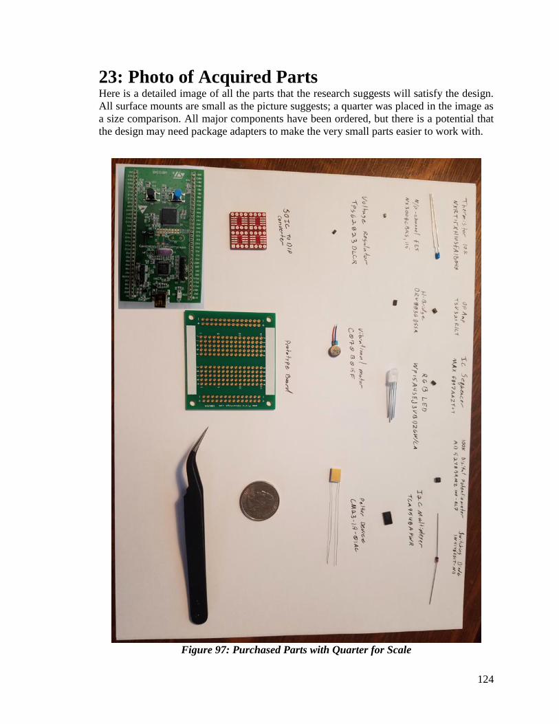
124
23: Photo of Acquired Parts Here is a detailed image of all the parts that the research suggests will satisfy the design.
All surface mounts are small as the picture suggests; a quarter was placed in the image as
a size comparison. All major components have been ordered, but there is a potential that
the design may need package adapters to make the very small parts easier to work with.
Figure 97: Purchased Parts with Quarter for Scale

125
24: References
[
1
]
"Project management guide: Tips, strategies, best practices," cio.com, 2017. [Online].
Available: https://www.cio.com/article/3243005/project-management/project-
management-tips-strategies-best-practices.htm. [Accessed July 2018].
[
2
]
[Online]. Available: http://merittechnology.sell.everychina.com/p-95148045-tes1-
03102-thermoelectric-cooling-modules.html.
[
3
]
[Online]. Available: https://cdn2.hubspot.net/hubfs/547732/Data_Sheets/CM23-
1.9.pdf.
[
4
]
[Online]. Available: https://www.meerstetter.ch/compendium/tec-peltier-element-
design-guide.
[
5
]
[Online]. Available: http://www.ti.com/lit/ds/symlink/drv8836.pdf.
[
6
]
[Online]. Available: http://www.analog.com/media/en/technical-documentation/data-
sheets/AD5243_5248.pdf.
[
7
]
[Online]. Available: https://www.st.com/resource/en/datasheet/tsv321.pdf.
[
8
]
[Online]. Available: https://assets.nexperia.com/documents/data-
sheet/NX3008CBKS.pdf.
[
9
]
[Online]. Available: https://en.wikipedia.org/wiki/PID_controller.
[
1
0
]
[Online]. Available:
https://www.murata.com/~/media/webrenewal/support/library/catalog/products/thermi
stor/ntc/r44e.ashx.
[
1
1
]
[Online]. Available: https://siliconlightworks.com/li-ion-voltage.
[
1
2
]
[Online]. Available: https://www.mouser.com/ds/2/737/C450_-
_ICR18650_6600mAh_3.7V_20140729-932760.pdf.
[
1
[Online]. Available: https://www.batteryspace.com/smartcharger30afor37vli-
ionpolymerrechargeablebatterypackstandardfemaletamiyaplug.aspx.

126
3
]
[
1
4
]
[Online]. Available: http://www.ti.com/lit/ds/slvsdv6b/slvsdv6b.pdf.
[
1
5
]
[Online]. Available: https://datasheets.maximintegrated.com/en/ds/MAX6895-
MAX6899.pdf.
[
1
6
]
[Online]. Available:
https://media.digikey.com/pdf/Data%20Sheets/Kingbright%20PDFs/WP154A4SEJ3
VBDZGW-CA_Ver.1A_Jul-24-13.pdf.
[
1
7
]
[Online]. Available: http://www.vibration-
motor.com/products/download/C0720B015F.pdf.
[
1
8
]
[Online]. Available: https://www.nxp.com/docs/en/data-sheet/MMA8451Q.pdf.
[
1
9
]
[Online]. Available: http://www.ti.com/lit/ds/symlink/tca9548a.pdf.
[
2
0
]
U. Lockhande, "Why to choose AVR Microcontroller?," BINARYUPDATES, 2018.
[Online]. Available: http://binaryupdates.com/why-to-choose-avr-microcontroller.
[Accessed July 2018].
[
2
1
]
"ATMEGA32U4-AU Microchip Technology," 2018. [Online]. Available:
https://www.mouser.com/ProductDetail/Microchip/ATMEGA32U4-
AU?qs=SSucg2PyLi7mKWjHIsNJ3w%3D%3D&gclid=CjwKCAjwyMfZBRAXEiw
A-R3gM6Magl9jTNJ4DxxI2TL- SDlLpPOExoCohsQAvD_BwE. [Accessed July
2018].
[
2
2
]
"MSP430G2553IPW28 Texas Instrument," 2018. [Online]. Available:
https://www.mouser.com/ProductDetail/Texas-
Instruments/MSP430G2553IPW28?qs=cBe3DO7yhR4cJ%252bt1uBW%252bXg%3
D%3D. [Accessed July 2018].
[
2
3
]
"STM32F030C8T6 STMicroelectronics," 2018. [Online]. Available:
https://www.mouser.com/ProductDetail/STMicroelectronics/STM32F030C8T6/?qs=e
yrSuY1LhL02NUjnPm0S4A%3d%3d&gclid=CjwKCAjwyMfZBRAXEiwA-
R3gM4ziVESe3M-UgbXVJw7RCOBeE3dmHc7JTBkx495riFrVBf-
KLN9VxxoC5hkQAvD_BwE. [Accessed July 2018].

127
[
2
4
]
"I2C Bus, Interface and Protocol.," I2C Info, 2018. [Online]. Available:
http://i2c.info/i2c-bus-specification. [Accessed July 2018].
[
2
5
]
"Back to Basics: The Universal Asynchronous Receiver/Transmitter (UART),"
Allaboutcircuits.com, 2018. [Online]. Available:
https://www.allaboutcircuits.com/technical-articles/back-to-basics-the-universal-
asynchronous-receiver-transmitter-uart/. [Accessed July 2018].
[
2
6
]
"Types of Wireless Communication and Its Applications," ElProCus, 2018. [Online].
Available: https://www.elprocus.com/types-of-wireless-communication-applications.
[Accessed July 2018].
[
2
7
]
"RN4871-V/RM118 Microchip Technology," Mouser Electronics, 2018. [Online].
Available: https://www.mouser.com/ProductDetail/Microchip/RN4871-V-
RM118?qs=U58vgkJzipTg3sP1%2Fz8hmA%3D%3D&gclid=CjwKCAjwsdfZBRAk
EiwAh2z65pNyNLuD5tGJ21kD3198Bxn1hMxVwAUdZkrwFgdMI_U7YtPGiCKTY
xoCRMIQAvD_BwE. [Accessed July 2018].
[
2
8
]
"BL652-SC-01 Lair," Mouser Electronics, 2018. [Online]. Available:
https://www.mouser.com/ProductDetail/Laird/BL652-SC-
01?qs=LuYMPh7GGMTBpPF65qWamA%3D%3D&gclid=CjwKCAjwsdfZBRAkEi
wAh2z65vw6Izf-
STGDpJXcDB1U99AzRHlkxrgEhFIsXsa6wJcJh2hoyiZ7zRoCCwQQAvD_BwE.
[Accessed July 2018].
[
2
9
]
"BM62SPKS1MC2-0001AA Microchip Technology," Mouser Electronics, 2018.
[Online]. Available: https://www.mouser.com/ProductDetail/Microchip-
Technology/BM62SPKS1MC2-
0001AA?qs=sGAEpiMZZMsGelYiB%252bjhZubn%252bI3eMtNUqLRpy06IcJEbW
6JnvgJ%2ftw%3d%3d. [Accessed July 2018].
[
3
0
]
"SOLIDWORKS PCB," TriMech, 2018. [Online]. Available:
https://trimech.com/products/3d-software/electronic-pcb/solidworks-pcb. [Accessed
July 2018].
[
3
1
]
"PCB Software," DesignSpark, 2018. [Online]. Available: https://www.rs-
online.com/designspark/pcb-software. [Accessed July 2018].
[
3
2
]
"PCB Prototype the Easy Way," Pcbway.com, 2018. [Online]. Available:
https://www.pcbway.com/. [Accessed July 2018].
[
3
3
]
"Standard & Custom Spec PCBs," 4pcb, 2018. [Online]. Available:
https://www.4pcb.com/pcb-manufacturing-custom-standard.html. [Accessed July
2018].

128
[
3
4
]
pcbgogo, 2018. [Online]. Available: https://www.pcbgogo.com/. [Accessed July 2018].
[
3
5
]
"PCB Prototype & PCB Fabrication Manufacturer," JLCPCB, 2018. [Online].
Available: https://jlcpcb.com/. [Accessed July 2018].
[
3
6
]
"Force Feedback Gloves for Virtual Reality," VRGluv, 2018. [Online]. Available:
https://vrgluv.com/. [Accessed July 2018].
[
3
7
]
"Haptic gloves for VR training, simulation, and design," HaptX, 2018. [Online].
Available: https://haptx.com/. [Accessed July 2018].
[
3
8
]
"What is JTAG and how can I make use of it?," XJTAG, 2018. [Online]. Available:
https://www.xjtag.com/about-jtag/what-is-jtag/. [Accessed July 2018].
[
3
9
]
mohammadalizadeh, "Realistic 3D Hand Model," 2018. [Online]. Available:
https://free3d.com/3d-model/freerealsichand-85561.htm. [Accessed July 2018].
[
4
0
]
"Free Sound Effects," 2018. [Online]. Available: https://www.freesoundeffects.com/.
[Accessed July 2018].
[
4
1
]
"Texture & Reference Image Library," 2018. [Online]. Available:
https://freetextures.3dtotal.com/index.php?la=1. [Accessed July 2018].
[
4
2
]
J. Ludwig, "Frequently Asked Questions," Valve, 2 August 2016. [Online]. Available:
https://steamcommunity.com/app/507090/discussions/0/360671247404603033/.
[Accessed July 2018].
[
4
3
]
dfelinto, "Virtual Reality Viewport," 25 July 2016. [Online]. Available:
https://github.com/dfelinto/virtual_reality_viewport).. [Accessed July 2018].
[
4
4
]
Blender, "Blender Python API Release 2.78," Blender, 2018. [Online]. Available:
https://docs.blender.org/api/blender_python_api_2_78_release/contents.html.
[Accessed July 2018].

129
[
4
5
]
[Online]. Available: https://visualstudio.microsoft.com/vs/older-downloads/.
[
4
6
]
[Online]. Available: https://en.wikipedia.org/wiki/Inter-process_communication.
[
4
7
]
[Online]. Available: https://docs.microsoft.com/en-
us/windows/desktop/bluetooth/about-bluetooth.
[
4
8
]
[Online]. Available: https://docs.microsoft.com/en-
us/windows/desktop/bluetooth/windows-sockets-support-for-bluetooth.
[
4
9
]
[Online]. Available:
https://www.bluetooth.org/docman/handlers/DownloadDoc.ashx?doc_id=86173.
[
5
0
]
[Online]. Available: https://en.wikipedia.org/wiki/Interpolation.
[
5
1
]
[Online]. Available: https://en.wikipedia.org/wiki/Linear_interpolation.
[
5
2
]
[Online]. Available: https://en.wikipedia.org/wiki/Linear_interpolation.
[
5
3
]
[Online]. Available: https://en.wikipedia.org/wiki/Unit_testing.
[
5
4
]
[Online]. Available: https://en.wikipedia.org/wiki/Integration_testing.
[
5
5
]
[Online]. Available: https://en.wikipedia.org/wiki/System_testing.

130
[
5
6
]
[Online]. Available: https://en.wikipedia.org/wiki/Test_management.
[
5
7
]
[Online]. Available: https://en.wikipedia.org/wiki/555_timer_IC.