Embed Size (px)
Citation preview

1
VDD
16
,1Å
2
CLMPI
3
OUTH 4
COM
5
AIN
12
6
DESAT
11
GND
7 10
8 9
VCC
Not to scale
OUTL
VEE
RDY
13
14 RST/EN
15
IN+
FLT
ISO
LA
TIO
N B
AR
RIE
RAPWM
Product
Folder
Order
Now
Technical
Documents
Tools &
Software
Support &Community
An IMPORTANT NOTICE at the end of this data sheet addresses availability, warranty, changes, use in safety-critical applications,intellectual property matters and other important disclaimers. PRODUCTION DATA.
UCC21750SLUSD78B –OCTOBER 2018–REVISED DECEMBER 2019
UCC21750 10-A Source/Sink Reinforced Isolated Single Channel Gate Driverfor SiC/IGBT with Active Protection, Isolated Analog Sensing and High-CMTI
1
1 Features1• 5.7-kVRMS single channel isolated gate driver• SiC MOSFETs and IGBTs up to 2121Vpk
• 33-V maximum output drive voltage (VDD-VEE)• ±10-A drive strength and split output• 150-V/ns minimum CMTI• 200-ns response time fast DESAT protection• 4-A Internal active miller clamp• 400-mA soft turn-off when fault happens• Isolated analog sensor with PWM output for
– Temperature sensing with NTC, PTC orthermal diode
– High voltage DC-Link or phase voltage• Alarm FLT on over current and reset from
RST/EN• Fast enable/disable response on RST/EN• Reject <40-ns noise transient and pulse on input
pins• 12-V VDD UVLO with power good on RDY• Inputs/outputs with over/under-shoot transient
voltage Immunity up to 5 V• 130-ns (maximum) propagation delay and 30-ns
(maximum) pulse/part skew• SOIC-16 DW package with creepage and
clearance distance > 8mm• Operating junction temperature –40°C to 150°C
2 Applications• Industrial motor drives• Server, telecom, and industrial power supplies• Uninterruptible power supplies (UPS)• Solar inverters
3 DescriptionThe UCC21750 is a galvanic isolated single channelgate driver designed for SiC MOSFETs and IGBTs upto 2121-V DC operating voltage with advancedprotection features, best-in-class dynamicperformance and robustness. UCC21750 has up to±10-A peak source and sink current.
The input side is isolated from the output side withSiO2 capacitive isolation technology, supporting up to1.5-kVRMS working voltage, 12.8-kVPK surge immunitywith longer than 40 years Isolation barrier life, as wellas providing low part-to-part skew, and >150V/nscommon mode noise immunity (CMTI).
The UCC21750 includes the state-of-art protectionfeatures, such as fast overcurrent and short circuitdetection, shunt current sensing support, faultreporting, active miller clamp, and input and outputside power supply UVLO to optimize SiC and IGBTswitching behavior and robustness. The isolatedanalog to PWM sensor can be utilized for easiertemperature or voltage sensing, further increasing thedrivers' versatility and simplifying the system designeffort, size and cost.
Device Information(1)
PART NUMBER PACKAGE BODY SIZE (NOM)UCC21750 DW SOIC-16 10.3 mm × 7.5 mm
(1) For all available packages, see the orderable addendum atthe end of the data sheet.
Device Pin Configuration

2
UCC21750SLUSD78B –OCTOBER 2018–REVISED DECEMBER 2019 www.ti.com
Product Folder Links: UCC21750
Submit Documentation Feedback Copyright © 2018–2019, Texas Instruments Incorporated
Table of Contents1 Features .................................................................. 12 Applications ........................................................... 13 Description ............................................................. 14 Revision History..................................................... 25 Pin Configuration and Functions ......................... 36 Specifications......................................................... 5
6.1 Absolute Maximum Ratings ..................................... 56.2 ESD Ratings ............................................................ 56.3 Recommended Operating Conditions....................... 56.4 Thermal Information .................................................. 56.5 Power Ratings........................................................... 66.6 Insulation Specifications............................................ 76.7 Safety-Related Certifications..................................... 86.8 Safety Limiting Values .............................................. 86.9 Electrical Characteristics........................................... 96.10 Switching Characteristics ...................................... 116.11 Insulation Characteristics Curves ......................... 126.12 Typical Characteristics .......................................... 13
7 Parameter Measurement Information ................ 177.1 Propagation Delay................................................... 177.2 Input Deglitch Filter ................................................. 197.3 Active Miller Clamp ................................................. 20
7.4 Under Voltage Lockout (UVLO) .............................. 217.5 Desaturation (DESAT) Protection ........................... 23
8 Detailed Description ............................................ 258.1 Overview ................................................................. 258.2 Functional Block Diagram ....................................... 268.3 Feature Description................................................. 268.4 Device Functional Modes........................................ 33
9 Applications and Implementation ...................... 349.1 Application Information............................................ 349.2 Typical Application .................................................. 34
10 Power Supply Recommendations ..................... 4511 Layout................................................................... 46
11.1 Layout Guidelines ................................................. 4611.2 Layout Example .................................................... 47
12 Device and Documentation Support ................. 4812.1 Documentation Support ....................................... 4812.2 Receiving Notification of Documentation Updates 4812.3 Community Resource............................................ 4812.4 Trademarks ........................................................... 4812.5 Electrostatic Discharge Caution............................ 4812.6 Glossary ................................................................ 48
13 Mechanical, Packaging, and OrderableInformation ........................................................... 48
4 Revision HistoryNOTE: Page numbers for previous revisions may differ from page numbers in the current version.
Changes from Revision A (April 2019) to Revision B Page
• Changed marketing status from Advance Information to production data. ............................................................................ 1
1
VDD
16
,1Å
2
CLMPI
3
OUTH 4
COM
5
AIN
12
6
DESAT
11
GND
7 10
8 9
VCC
Not to scale
OUTL
VEE
RDY
13
14 RST/EN
15
IN+
FLT
ISO
LA
TIO
N B
AR
RIE
R
APWM
3
UCC21750www.ti.com SLUSD78B –OCTOBER 2018–REVISED DECEMBER 2019
Product Folder Links: UCC21750
Submit Documentation FeedbackCopyright © 2018–2019, Texas Instruments Incorporated
5 Pin Configuration and Functions
UCC21750DW SOIC (16)
Top View

4
UCC21750SLUSD78B –OCTOBER 2018–REVISED DECEMBER 2019 www.ti.com
Product Folder Links: UCC21750
Submit Documentation Feedback Copyright © 2018–2019, Texas Instruments Incorporated
(1) P = Power, G = Ground, I = Input, O = Output
Pin FunctionsPIN
I/O (1) DESCRIPTIONNAME NO.AIN 1 I Isolated analog sensing input, parallel a small capacitor to COM for better noise immunityDESAT 2 I Desaturation current protection inputCOM 3 P Common ground reference, connecting to emitter pin for IGBT and source pin for SiC-MOSFETOUTH 4 O Gate driver output pull up
VDD 5 P Positive supply rail for gate drive voltage, Bypassing a >220nF capacitor to COM to support specified gatedriver source peak current capability
OUTL 6 O Gate driver output pull downCLMPI 7 I Internal Active miller clamp, connecting this pin directly to the gate of the power transistor
VEE 8 P Negative supply rail for gate drive voltage. Bypassing a >220nF capacitor to COM to support specified gatedriver sink peak current capability
GND 9 P Input power supply and logic ground referenceIN+ 10 I Non-inverting gate driver control inputIN– 11 I Inverting gate driver control input
RDY 12 O Power good for VCC-GND and VDD-COM. RDY is open drain configuration and can be paralleled with otherRDY signals
FLT 13 O Active low fault alarm output upon over current or short circuit. FLT is in open drain configuration and can beparalleled with other faults
RST/EN 14 I
The RST/EN serves two purposes:1) Enable / shutdown of the output side. The FET is turned off by a general turn-off, if terminal EN is set tolow;2) Resets the DESAT condition signaled on FLT pin. if terminal RST/EN is set to low for more than 1000ns.A reset of signal FLT is asserted at the rising edge of terminal RST/EN.For automatic RESET function, this pin only serves as an EN pin. Enable / shutdown of the output side. TheFET is turned off by a general turn-off, if terminal EN is set to low.
VCC 15 P Input power supply from 3V to 5.5V, bypassing a >100nF capacitor to GNDAPWM 16 O Isolated Analog Sensing PWM output
5
UCC21750www.ti.com SLUSD78B –OCTOBER 2018–REVISED DECEMBER 2019
Product Folder Links: UCC21750
Submit Documentation FeedbackCopyright © 2018–2019, Texas Instruments Incorporated
(1) Stresses beyond those listed under absolute maximum ratings may cause permanent damage to the device. These are stress ratingsonly and functional operation of the device at these or any other conditions beyond those indicated under recommended operatingconditions is not implied. Exposure to absolute-maximum-rated conditions for extended periods may affect device reliability.
(2) Values are verified by characterization on bench.
6 Specifications
6.1 Absolute Maximum Ratingsover operating free-air temperature range (unless otherwise noted) (1)
PARAMETER MIN MAX UNITVCC VCC – GND –0.3 6 VVDD VDD – COM –0.3 36 VVEE VEE – COM –17.5 0.3 VVMAX VDD – VEE –0.3 36 V
IN+, IN–, RST/ENDC GND–0.3 VCC VTransient, less than 100 ns (2) GND–5.0 VCC+5.0 V
DESAT Reference to COM COM–0.3 VDD+0.3 VAIN Reference to COM –0.3 5 V
OUTH, OUTL , CLMPIDC VEE–0.3 VDD VTransient, less than 100 ns (2) VEE–5.0 VDD+5.0 V
RDY, FLT, APWM GND–0.3 VCC VIFLT, IRDY FLT, and RDY pin input current 20 mAIAPWM APWM pin output current 20 mATJ Junction temperature range –40 150 °CTstg Storage temperature range –65 150 °C
(1) AEC Q100-002 indicates that HBM stressing shall be in accordance with the ANSI/ESDA/JEDEC JS-001 specification.
6.2 ESD RatingsVALUE UNIT
V(ESD) Electrostatic dischargeHuman-body model (HBM), per AEC Q100-002 (1) ±4000
VCharged-device model (CDM), per AEC Q100-011 ±1500
6.3 Recommended Operating ConditionsPARAMETER MIN MAX UNITVCC VCC–GND 3.0 5.5 VVDD VDD–COM 13 33 VVMAX VDD–VEE – 33 V
IN+, IN–, RST/EN Reference to GNDHigh level input voltage 0.7×VCC VCC
VLow level input voltage 0 0.3×VCC
AIN Reference to COM 0.6 4.5 VtRST/EN Minimum pulse width that reset the fault 1000 nsTA Ambient Temperature –40 125 °CTJ Junction temperature –40 150 °C
(1) For more information about traditional and new thermal metrics, see the Semiconductor and IC Package Thermal Metrics applicationreport.
6.4 Thermal Information
THERMAL METRIC (1)UCC21750
UNITDW (SOIC)16
RθJA Junction-to-ambient thermal resistance 68.3 °C/WRθJC(top) Junction-to-case (top) thermal resistance 27.5 °C/W

6
UCC21750SLUSD78B –OCTOBER 2018–REVISED DECEMBER 2019 www.ti.com
Product Folder Links: UCC21750
Submit Documentation Feedback Copyright © 2018–2019, Texas Instruments Incorporated
Thermal Information (continued)
THERMAL METRIC (1)UCC21750
UNITDW (SOIC)16
RθJB Junction-to-board thermal resistance 32.9 °C/WψJT Junction-to-top characterization parameter 14.1 °C/WψJB Junction-to-board characterization parameter 32.3 °C/W
6.5 Power RatingsPARAMETER TEST CONDITIONS Value UNIT
PDMaximum power dissipation (bothsides)
VCC = 5V, VDD-COM = 20V, COM-VEE = 5V, IN+/- = 5V, 150kHz,50% Duty Cycle for 10nF load, Ta=25oC
985 mW
PD1Maximum power dissipation bytransmitter side 20 mW
PD2Maximum power dissipation byreceiver side 965 mW
7
UCC21750www.ti.com SLUSD78B –OCTOBER 2018–REVISED DECEMBER 2019
Product Folder Links: UCC21750
Submit Documentation FeedbackCopyright © 2018–2019, Texas Instruments Incorporated
(1) Apply creepage and clearance requirements according to the specific equipment isolation standards of an application. Care must betaken to maintain the creepage and clearance distance of a board design to ensure that the mounting pads of the isolator on the printedcircuit board (PCB) do not reduce this distance. Creepage and clearance on a PCB become equal in certain cases. Techniques such asinserting grooves and ribs on the PCB are used to help increase these specifications.
(2) This coupler is suitable for safe electrical insulation only within the safety ratings. Compliance with the safety ratings shall be ensured bymeans of suitable protective circuits.
(3) Testing is carried out in air or oil to determine the intrinsic surge immunity of the isolation barrier.(4) Apparent charge is electrical discharge caused by a partial discharge (pd).(5) All pins on each side of the barrier tied together creating a two-terminal device
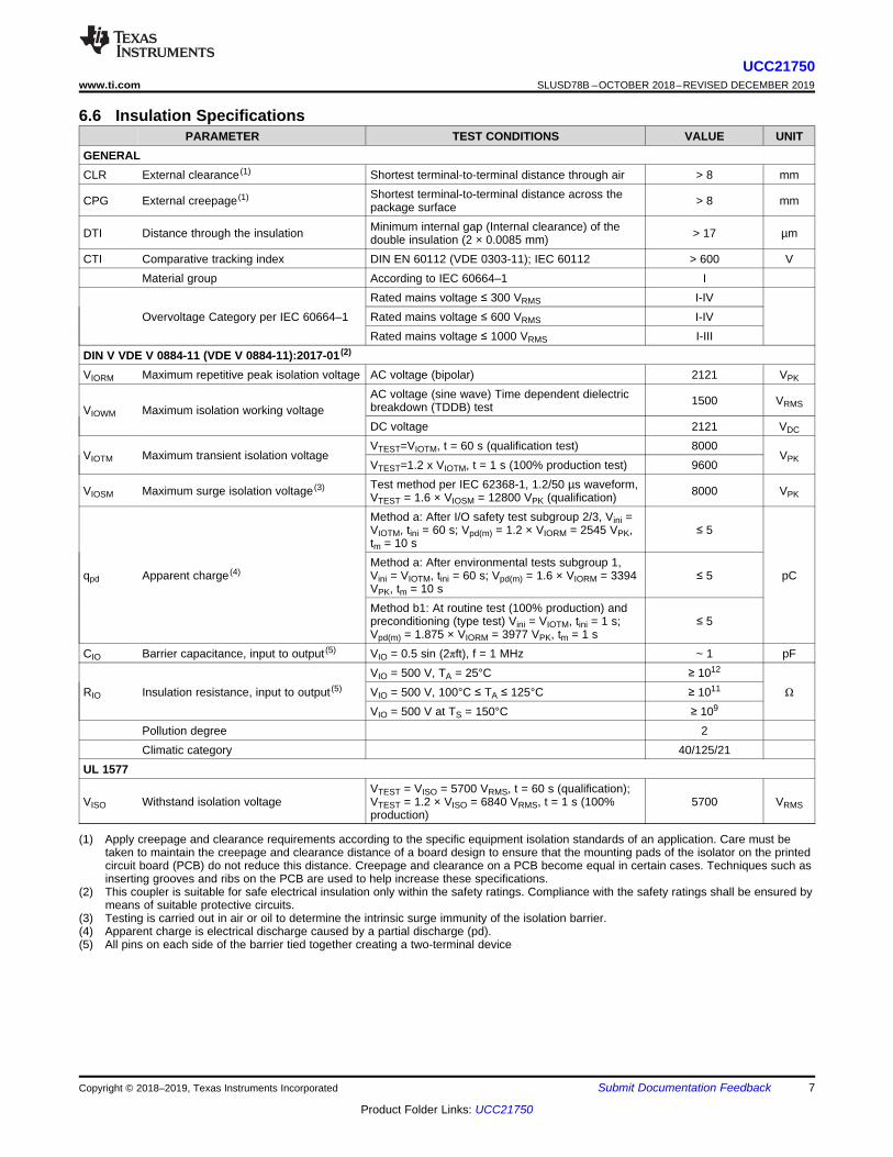
6.6 Insulation SpecificationsPARAMETER TEST CONDITIONS VALUE UNIT
GENERALCLR External clearance (1) Shortest terminal-to-terminal distance through air > 8 mm
CPG External creepage (1) Shortest terminal-to-terminal distance across thepackage surface > 8 mm
DTI Distance through the insulation Minimum internal gap (Internal clearance) of thedouble insulation (2 × 0.0085 mm) > 17 µm
CTI Comparative tracking index DIN EN 60112 (VDE 0303-11); IEC 60112 > 600 VMaterial group According to IEC 60664–1 I
Overvoltage Category per IEC 60664–1Rated mains voltage ≤ 300 VRMS I-IVRated mains voltage ≤ 600 VRMS I-IVRated mains voltage ≤ 1000 VRMS I-III
DIN V VDE V 0884-11 (VDE V 0884-11):2017-01 (2)
VIORM Maximum repetitive peak isolation voltage AC voltage (bipolar) 2121 VPK
VIOWM Maximum isolation working voltageAC voltage (sine wave) Time dependent dielectricbreakdown (TDDB) test 1500 VRMS
DC voltage 2121 VDC
VIOTM Maximum transient isolation voltageVTEST=VIOTM, t = 60 s (qualification test) 8000
VPKVTEST=1.2 x VIOTM, t = 1 s (100% production test) 9600
VIOSM Maximum surge isolation voltage (3) Test method per IEC 62368-1, 1.2/50 µs waveform,VTEST = 1.6 × VIOSM = 12800 VPK (qualification) 8000 VPK
qpd Apparent charge (4)
Method a: After I/O safety test subgroup 2/3, Vini =VIOTM, tini = 60 s; Vpd(m) = 1.2 × VIORM = 2545 VPK,tm = 10 s
≤ 5
pCMethod a: After environmental tests subgroup 1,Vini = VIOTM, tini = 60 s; Vpd(m) = 1.6 × VIORM = 3394VPK, tm = 10 s
≤ 5
Method b1: At routine test (100% production) andpreconditioning (type test) Vini = VIOTM, tini = 1 s;Vpd(m) = 1.875 × VIORM = 3977 VPK, tm = 1 s
≤ 5
CIO Barrier capacitance, input to output (5) VIO = 0.5 sin (2πft), f = 1 MHz ~ 1 pF
RIO Insulation resistance, input to output (5)
VIO = 500 V, TA = 25°C ≥ 1012
ΩVIO = 500 V, 100°C ≤ TA ≤ 125°C ≥ 1011
VIO = 500 V at TS = 150°C ≥ 109
Pollution degree 2Climatic category 40/125/21
UL 1577
VISO Withstand isolation voltageVTEST = VISO = 5700 VRMS, t = 60 s (qualification);VTEST = 1.2 × VISO = 6840 VRMS, t = 1 s (100%production)
5700 VRMS

8
UCC21750SLUSD78B –OCTOBER 2018–REVISED DECEMBER 2019 www.ti.com
Product Folder Links: UCC21750
Submit Documentation Feedback Copyright © 2018–2019, Texas Instruments Incorporated
6.7 Safety-Related CertificationsVDE UL CSA CQC TUV
Plan to certify accordingto DIN V VDE V 0884-11(VDE V 0884-11):2017-01;DIN EN 61010-1 (VDE0411-1):2011-07
Plan to certifyaccording toUL 1577ComponentRecognitionProgram
Plan to certify according toCSA Component AcceptanceNotice 5A, IEC 60950-1, andIEC 60601-1
Plan to certify according toGB4943.1-2011
Plan to certify according toEN 61010-1:2010 (3rd Ed)andEN 60950-1:2006/A11:2009/A1:2010/A12:2011/A2:2013
Reinforced insulationMaximum transientisolation voltage, 8000VPK;Maximum repetitive peakisolation voltage, 2121VPK;Maximum surge isolationvoltage, 8000 VPK
Singleprotection,5700 VRMS
Isolation Rating of 5700 VRMS;Reinforced insulation per CSA60950-1- 07+A1+A2 and IEC60950-1 (2nd Ed.), 1450 VRMSmax working voltage (pollutiondegree 2, material group I) ;2 MOPP (Means of PatientProtection) per CSA 60601-1:14 and IEC 60601-1 Ed. 3.1,250 VRMS (354 VPK) maxworking voltage
Reinforced Insulation, Altitude≤ 5000m, Tropical climate,400 VRMS maximum workingvoltage
5700 VRMS Reinforcedinsulation perEN 61010-1:2010 (3rd Ed) upto working voltage of 1000VRMS5700 VRMS Reinforcedinsulation perEN 60950-1:2006/A11:2009/A1:2010/A12:2011/A2:2013 up toworking voltage of 1450 VRMS
Certification Planned CertificationPlanned Certification Planned Certification Planned Certification Planned
(1) The safety-limiting constraint is the maximum junction temperature specified in the data sheet. The power dissipation and junction-to-airthermal impedance of the device installed in the application hardware determines the junction temperature. The assumed junction-to-airthermal resistance in the Thermal Information table is that of a device installed on a high-K test board for leaded surface-mountpackages. The power is the recommended maximum input voltage times the current. The junction temperature is then the ambienttemperature plus the power times the junction-to-air thermal resistance.
6.8 Safety Limiting ValuesSafety limiting (1) intends to minimize potential damage to the isolation barrier upon failure of input or output circuitry. A failureof the I/O can allow low resistance to ground or the supply and, without current limiting, dissipate sufficient power to overheatthe die and damage the isolation barrier, potentially leading to secondary system failures.
PARAMETER TEST CONDITIONS MIN TYP MAX UNIT
ISSafety input, output, or supplycurrent
RθJA =68.3°C/W, VDD = 15V, VEE=-5V, TJ = 150°C, TA= 25°C 61
mARθJA =68.3°C/W, VDD = 20V, VEE=-5V, TJ = 150°C, TA= 25°C 49
PSSafety input, output, or totalpower
RθJA =68.3°C/W, VDD = 20V, VEE=-5V, TJ = 150°C, TA= 25°C 1220 mW
TS Safety temperature 150 °C

9
UCC21750www.ti.com SLUSD78B –OCTOBER 2018–REVISED DECEMBER 2019
Product Folder Links: UCC21750
Submit Documentation FeedbackCopyright © 2018–2019, Texas Instruments Incorporated
(1) Current are positive into and negative out of the specified terminal.(2) All voltages are referenced to COM unless otherwise notified.
6.9 Electrical CharacteristicsVCC = 3.3 V or 5.0 V, 1-µF capacitor from VCC to GND, VDD – COM = 20 V, 18 V or 15 V, COM – VEE = 0 V, 5 V, 8 V or15 V, CL = 100 pF, –40°C < TJ < 150°C (unless otherwise noted) (1) (2).
PARAMETER TEST CONDITIONS MIN TYP MAX UNIT
VCC UVLO THRESHOLD AND DELAY
VVCC_ON
VCC–GND
2.55 2.7 2.85
VVVCC_OFF 2.35 2.5 2.65
VVCC_HYS 0.2
tVCCFIL VCC UVLO Deglitch time 10
µs
tVCC+ to OUT VCC UVLO on delay to output highIN+ = VCC, IN– = GND
28 37.8 50
tVCC– to OUT VCC UVLO off delay to output low 5 10 15
tVCC+ to RDY VCC UVLO on delay to RDY highRST/EN = VCC
30 37.8 50
tVCC– to RDY VCC UVLO off delay to RDY low 5 10 15
VDD UVLO THRESHOLD AND DELAY
VVDD_ON
VDD–COM
10.5 12.0 12.8
VVVDD_OFF 9.9 10.7 11.8
VVDD_HYS 0.8
tVDDFIL VDD UVLO Deglitch time 5
µs
tVDD+ to OUT VDD UVLO on delay to output highIN+ = VCC, IN– = GND
2 5 8
tVDD– to OUT VDD UVLO off delay to output low 5 10
tVDD+ to RDY VDD UVLO on delay to RDY highRST/EN = FLT=High
10 15
tVDD– to RDY VDD UVLO off delay to RDY low 10 15
VCC, VDD QUIESCENT CURRENT
IVCCQ VCC quiescent currentOUT(H) = High, fS = 0Hz, AIN=2V 2.5 3 4
mAOUT(L) = Low, fS = 0Hz, AIN=2V 1.45 2 2.75
IVDDQ VDD quiescent currentOUT(H) = High, fS = 0Hz, AIN=2V 3.6 4 5.9
mAOUT(L) = Low, fS = 0Hz, AIN=2V 3.1 3.7 5.3
LOGIC INPUTS — IN+, IN– and RST/EN
VINH Input high threshold VCC=3.3V 1.85 2.31 V
VINL Input low threshold VCC=3.3V 0.99 1.52 V
VINHYS Input threshold hysteresis VCC=3.3V 0.33 V
IIH Input high level input leakage current VIN = VCC 90 µA
IIL Input low level input leakage VIN = GND –90 µA
RIND Input pins pull down resistance see Detailed Description for moreinformation 28.5 55 113
kΩRINU Input pins pull up resistance see Detailed Description for more
information 28.5 55 113
TINFILIN+, IN– and RST/EN deglitch (ON andOFF) filter time fS = 50kHz 28 40 60 ns
TRSTFIL Deglitch filter time to reset /FLT 400 650 800 ns
GATE DRIVER STAGE
IOUT, IOUTH Peak source currentCL=0.18µF, fS=1kHz
10 A
IOUT, IOUTL Peak sink current 10 A
ROUTH Output pull-up resistance IOUT = –0.1A 1.5 2.5 4.9 Ω
ROUTL Output pull-down resistance IOUT = 0.1A 0.1 0.3 0.7 Ω
VOUTH High level output voltage IOUT = –0.2A, VDD=18V 17.5 V
VOUTL Low level output voltage IOUT = 0.2A 60 mV
ACTIVE PULLDOWN
VOUTPD Output active pull down on OUT, OUTL IOUTL or IOUT = 0.1×IOUT(L)(tpy),VDD=OPEN, VEE=COM 1.5 2 2.5 V
INTERNAL ACTIVE MILLER CLAMP
VCLMPTH Miller clamp threshold voltage Reference to VEE 1.5 2.0 2.5 V
VCLMPI Output low clamp voltage ICLMPI = 1A VEE + 0.5 V

10
UCC21750SLUSD78B –OCTOBER 2018–REVISED DECEMBER 2019 www.ti.com
Product Folder Links: UCC21750
Submit Documentation Feedback Copyright © 2018–2019, Texas Instruments Incorporated
Electrical Characteristics (continued)VCC = 3.3 V or 5.0 V, 1-µF capacitor from VCC to GND, VDD – COM = 20 V, 18 V or 15 V, COM – VEE = 0 V, 5 V, 8 V or15 V, CL = 100 pF, –40°C < TJ < 150°C (unless otherwise noted)(1)(2).
PARAMETER TEST CONDITIONS MIN TYP MAX UNIT
ICLMPI Output low clamp current VCLMPI = 0V, VEE = –2.5V 4 A
RCLMPI Miller clamp pull down resistance ICLMPI = 0.2A 0.6 Ω
tDCLMPI Miller clamp ON delay time CL = 1.8nF 15 50 ns
SHORT CIRCUIT CLAMPING
VCLP-OUT(H) VOUT–VDD, VOUTH–VDD OUT = Low, IOUT(H) = 500mA, tCLP=10us 0.9 0.99 V
VCLP-OUT(L) VOUT–VDD, VOUTL–VDD OUT = High, IOUT(L) = 500mA, tCLP=10us 1.8 1.98 V
VCLP-CLMPI VCLMPI–VDD OUT = High, ICLMPI = -20mA, tCLP=10us 1.0 V
DESAT PROTECTION
ICHG Blanking capacitor charge current VDESAT = 2.0V 445 500 570 µA
IDCHG Blanking capacitor discharge current VDESAT = 6.0V 10 15 mA
VDESAT Detection Threshold 8.2 9.1 10 V
VDESATLVoltage when OUT(L) = LOW, Referenceto COM IDESAT = 15mA 1 V
tDESATLEB Leading edge blank time 150 200 450 ns
tDESATFIL DESAT deglitch filter 50 150 350 ns
tDESATOFF DESAT propagation delay to OUT(L) 90% 150 200 300 ns
tDESATFLT DESAT to FLT low delay 300 600 750 ns
INTERNAL SOFT TURN-OFF
ISTO Soft turn-off current on fault conditions 250 400 570 mA
ISOLATED TEMPERATURE SENSE AND MONITOR (AIN–APWM)
VAIN Analog sensing voltage range 0.5 4.5 V
IAIN Internal current source VAIN=2.5V, -40°C< TJ< 150°C 196 200 209 µA
fAPWM APWM output frequency VAIN=2.5V 380 400 420 kHz
BWAIN AIN–APWM bandwidth 10 kHz
DAPWM APWM Dutycycle
VAIN = 0.6V 86.5 88 89.5
%VAIN = 2.5V 48.5 50 51.5
VAIN = 4.5V 7.5 10 11.5
FLT AND RDY REPORTING
tRDYHLDVDD UVLO RDY low minimum holdingtime 0.55 1 ms
tFLTMUTE Output mute time on fault Reset fault through RST/EN 0.55 1 ms
RODON Open drain output on resistance IODON = 5mA 30 Ω
VODL Open drain low output voltage IODON = 5mA 0.3 V
COMMON MODE TRANSIENT IMMUNITY
CMTI Common-mode transient immunity 150 V/ns

11
UCC21750www.ti.com SLUSD78B –OCTOBER 2018–REVISED DECEMBER 2019
Product Folder Links: UCC21750
Submit Documentation FeedbackCopyright © 2018–2019, Texas Instruments Incorporated
6.10 Switching CharacteristicsVCC=5.0V, 1uF capacitor from VCC to GND, VDD–COM=20V, 18V or 15V, COM–VEE = 3V, 5V or 8V, CL=100pF,–40°C<TJ<150°C (unless otherwise noted)
PARAMETER TEST CONDITIONS MIN TYP MAX UNIT
tPDHL Propagation delay time – High to Low 60 90 130
ns
tPDLH Propagation delay time – Low to High 60 90 130
PWD Pulse width distortion |tPDHL – tPDLH| 30
tsk-pp Part to Part skew Rising or Falling Propagation Delay 30
tr Driver output rise time CL=10nF 33
tf Driver output fall time CL=10nF 27
fMAX Maximum switching frequency 1 MHz

Ambient Temperature (oC)
Sa
fety
Lim
itin
g C
urr
ent (m
A)
0 25 50 75 100 125 1500
20
40
60
80
Safe
VDD=15V; VEE=-5VVDD=20V; VEE=-5V
Ambient Temperature (oC)
Sa
fety
Lim
itin
g P
ow
er
(mW
)
0 20 40 60 80 100 120 140 1600
200
400
600
800
1000
1200
1400
Safe
1.E+01
1.E+02
1.E+03
1.E+04
1.E+05
1.E+06
1.E+07
1.E+08
1.E+09
1.E+10
1.E+11
1.E+12
200 1200 2200 3200 4200 5200 6200
Tim
e t
o F
ail
(se
c)
Applied Voltage (VRMS)
54 Yrs
TDDB Line (< 1 ppm Fail Rate)
VDE Safety Margin Zone
1800VRMS
12
UCC21750SLUSD78B –OCTOBER 2018–REVISED DECEMBER 2019 www.ti.com
Product Folder Links: UCC21750
Submit Documentation Feedback Copyright © 2018–2019, Texas Instruments Incorporated
6.11 Insulation Characteristics Curves
Figure 1. Reinforced Isolation Capacitor Life Time Projection
Figure 2. Thermal Derating Curve for Limiting Current perVDE
Figure 3. Thermal Derating Curve for Limiting Power perVDE
Frequency (kHz)
I VC
CQ
(m
A)
30 70 110 150 190 230 270 3102
2.5
3
3.5
4
4.5
5
D018
VDD/VEE = 18V/0VVDD/VEE = 20V/-5V
Temperature (qC)
I VD
DQ
(m
A)
-60 -40 -20 0 20 40 60 80 100 120 140 1603
3.5
4
4.5
5
5.5
6
D012
VDD/VEE = 18V/0VVDD/VEE = 20V/-5V
Temperature (qC)
I VC
CQ
(m
A)
-60 -40 -20 0 20 40 60 80 100 120 140 1603
3.5
4
4.5
5
5.5
6
D015
VCC = 3.3VVCC = 5V
Temperature (qC)
I VC
CQ
(m
A)
-60 -40 -20 0 20 40 60 80 100 120 140 1601
1.5
2
2.5
3
3.5
4
D014
VCC = 3.3VVCC = 5V
Temperature (qC)
Peak O
utp
ut C
urr
ent
Hig
h,
I OU
TH
(A
)
-60 -40 -20 0 20 40 60 80 100 120 140 1604
6
8
10
12
14
16
18
20
22
D016
VDD/VEE = 18V/0VVDD/VEE = 20V/-5V
Temperature (qC)
Peak O
utp
ut C
urr
ent Low
, I O
UT
L (
A)
-60 -40 -20 0 20 40 60 80 100 120 140 1604
6
8
10
12
14
16
18
20
22
D017
VDD/VEE = 18V/0VVDD/VEE = 20V/-5V
13
UCC21750www.ti.com SLUSD78B –OCTOBER 2018–REVISED DECEMBER 2019
Product Folder Links: UCC21750
Submit Documentation FeedbackCopyright © 2018–2019, Texas Instruments Incorporated
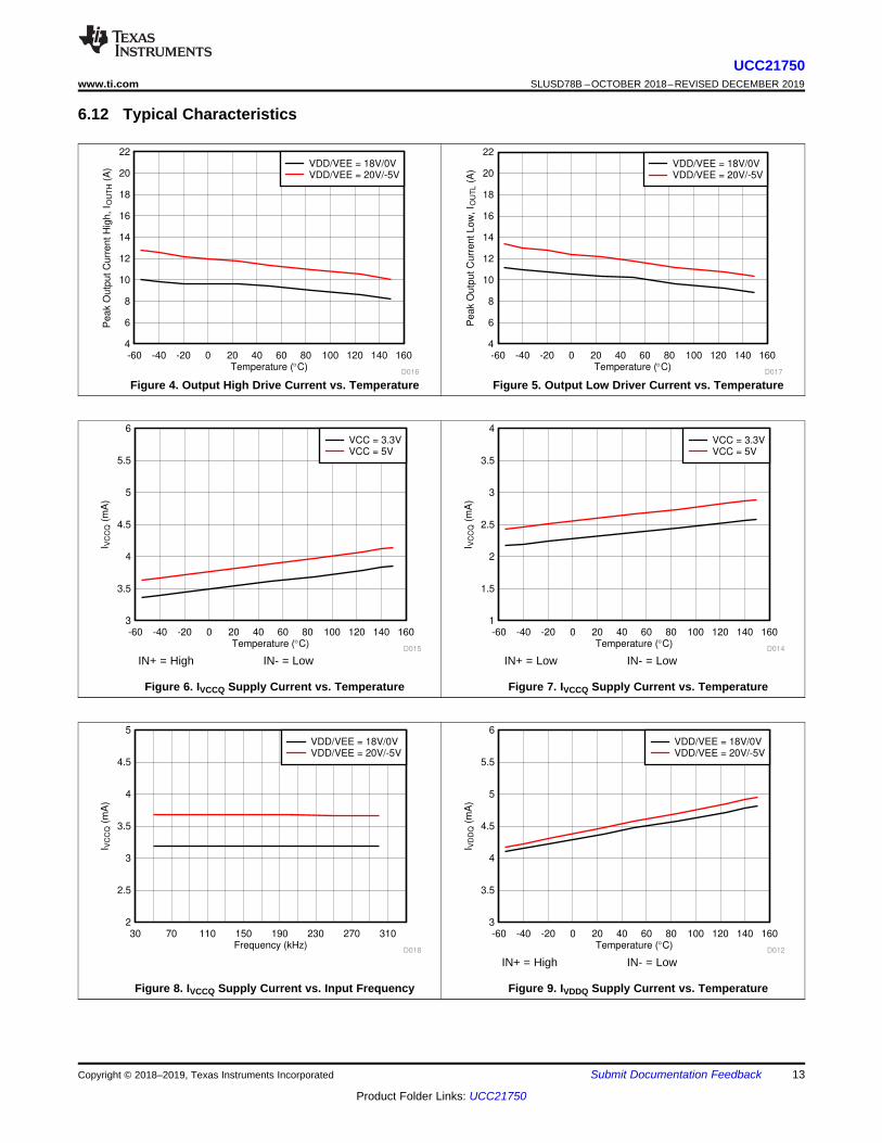
6.12 Typical Characteristics
Figure 4. Output High Drive Current vs. Temperature Figure 5. Output Low Driver Current vs. Temperature
IN+ = High IN- = Low
Figure 6. IVCCQ Supply Current vs. Temperature
IN+ = Low IN- = Low
Figure 7. IVCCQ Supply Current vs. Temperature
Figure 8. IVCCQ Supply Current vs. Input Frequency
IN+ = High IN- = Low
Figure 9. IVDDQ Supply Current vs. Temperature

Temperature (qC)
Pro
paga
tion D
ela
y L
ow
-Hig
h,
t PD
LH (
ns)
-60 -40 -20 0 20 40 60 80 100 120 140 16050
60
70
80
90
100
D021Temperature (qC)
Pro
paga
tion D
ela
y H
igh-L
ow
, t P
DH
L (
ns)
-60 -40 -20 0 20 40 60 80 100 120 140 16050
60
70
80
90
100
D022
Temperature (qC)
VC
C U
VLO
Th
reshold
, V
CC
_O
N (
V)
-60 -40 -20 0 20 40 60 80 100 120 140 1601.5
2
2.5
3
3.5
4
D001Temperature (qC)
VD
D U
VLO
Th
reshold
, V
DD
_O
N (
V)
-60 -40 -20 0 20 40 60 80 100 120 140 16010
10.5
11
11.5
12
12.5
13
13.5
14
D002
Temperature (qC)
I VD
DQ
(m
A)
-60 -40 -20 0 20 40 60 80 100 120 140 1603
3.5
4
4.5
5
5.5
6
D013
VDD/VEE = 18V/0VVDD/VEE = 20V/-5V
Frequency (kHz)
I VD
DQ
(m
A)
30 70 110 150 190 230 270 3102
3
4
5
6
7
8
9
10
D019
VDD/VEE = 18V/0VVDD/VEE = 20V/-5V
14
UCC21750SLUSD78B –OCTOBER 2018–REVISED DECEMBER 2019 www.ti.com
Product Folder Links: UCC21750
Submit Documentation Feedback Copyright © 2018–2019, Texas Instruments Incorporated
Typical Characteristics (continued)
IN+ = Low IN- = Low
Figure 10. IVDDQ Supply Current vs. Temperature Figure 11. IVDDQ Supply Current vs. Input Frequency
Figure 12. VCC UVLO vs. Temperature Figure 13. VDD UVLO vs. Temperature
VCC = 3.3V VDD=18V CL = 100pFRON = 0Ω ROFF = 0Ω
Figure 14. Propagation Delay tPDLH vs. Temperature
VCC = 3.3V VDD=18V CL = 100pFRON = 0Ω ROFF = 0Ω
Figure 15. Propagation Delay tPDHL vs. Temperature

Temperature (qC)
VC
LP
-OU
T(L
) (V
)
-60 -40 -20 0 20 40 60 80 100 120 140 1600.25
0.5
0.75
1
1.25
1.5
1.75
2
D026Temperature (°C)
Mill
er
Cla
mp T
hre
sh
old
Vo
lta
ge
, V
CL
MP
TH (
V)
-60 -40 -20 0 20 40 60 80 100 120 140 1601.4
1.55
1.7
1.85
2
2.15
2.3
2.45
2.6
D007
Temperature (qC)
VC
LP
-OU
T(H
) (V
)
-60 -40 -20 0 20 40 60 80 100 120 140 1601
1.25
1.5
1.75
2
2.25
2.5
D025
Temperature (qC)
VO
UT
PD (
V)
-60 -40 -20 0 20 40 60 80 100 120 140 1601.5
1.75
2
2.25
2.5
2.75
3
D008
Temperature (qC)
Ris
e T
ime,
t r (
ns)
-60 -40 -20 0 20 40 60 80 100 120 140 16010
20
30
40
50
60
D023Temperature (qC)
Fall
Tim
e, t f (
ns)
-60 -40 -20 0 20 40 60 80 100 120 140 16010
20
30
40
50
60
D024
15
UCC21750www.ti.com SLUSD78B –OCTOBER 2018–REVISED DECEMBER 2019
Product Folder Links: UCC21750
Submit Documentation FeedbackCopyright © 2018–2019, Texas Instruments Incorporated
Typical Characteristics (continued)
VCC = 3.3V VDD=18V CL = 10nFRON = 0Ω ROFF = 0Ω
Figure 16. tr Rise Time vs. Temperature
VCC = 3.3V VDD=18V CL = 10nFRON = 0Ω ROFF = 0Ω
Figure 17. tf Fall Time vs. Temperature
Figure 18. VOUTPD Output Active Pulldown Voltage vs.Temperature
Figure 19. VCLP-OUT(H) Short Circuit Clamping Voltage vs.Temperature
Figure 20. VCLP-OUT(L) Short Circuit Clamping Voltage vs.Temperature
Figure 21. VCLMPTH Miller Clamp Threshold Voltage vs.Temperature

Temperature (°C)
DE
SA
T P
ropagation D
ela
y to O
UT
(L)
90%
, t D
ES
AT
OF
F (
ns)
-60 -40 -20 0 20 40 60 80 100 120 140 160200
210
220
230
240
250
260
270
280
290
300
D003
Temperature (°C)
DE
SA
T S
ense to /F
LT
Low
Dela
y, t D
ES
AT
FLT (
ns)
-60 -40 -20 0 20 40 60 80 100 120 140 160500
520
540
560
580
600
620
640
660
680
D004
Temperature (°C)
DE
SA
T T
hre
shold
Voltage, V
DE
SA
T (
V)
-60 -40 -20 0 20 40 60 80 100 120 140 1608
8.2
8.4
8.6
8.8
9
9.2
9.4
9.6
9.8
10
D001Temperature (°C)
Le
ad
ing
Ed
ge
Bla
nkin
g T
ime
, t D
ES
AT
LE
B (
ns)
-60 -40 -20 0 20 40 60 80 100 120 140 160100
140
180
220
260
300
340
380
420
D002
Temperature (qC)
Peak C
lam
p S
ink C
urr
ent, I
CL
MP
I (A
)
-60 -40 -20 0 20 40 60 80 100 120 140 1600.5
1.5
2.5
3.5
4.5
5.5
6.5
7.5
8.5
D011Temperature (°C)
Mill
er
Cla
mp O
N D
ela
y T
ime, t D
CL
MP
I (ns)
-60 -40 -20 0 20 40 60 80 100 120 140 16010
11
12
13
14
15
16
17
18
D010
16
UCC21750SLUSD78B –OCTOBER 2018–REVISED DECEMBER 2019 www.ti.com
Product Folder Links: UCC21750
Submit Documentation Feedback Copyright © 2018–2019, Texas Instruments Incorporated
Typical Characteristics (continued)
Figure 22. ICLMPI Miller Clamp Sink Current vs. Temperature Figure 23. tDCLMPI Miller Clamp ON Delay Time vs.Temperature
Figure 24. VDESAT DESAT Threshold Voltage vs.Temperature
Figure 25. tDESATLEB DESAT Leading Edge Blanking Time vs.Temperature
Figure 26. tDESATOFF DESAT Propagation Delay to OUT(L)90% vs. Temperature
Figure 27. tDESATFLT DESAT Sense to /FLT Low Delay Timevs. Temperature

Temperature (°C)
DE
SA
T D
ischarg
e C
urr
ent, I
DC
HG
(P
A)
-60 -40 -20 0 20 40 60 80 100 120 140 16010
11
12
13
14
15
16
17
18
19
20
D009
Temperature (°C)
DE
SA
T D
eg
litch F
ilte
r, t
DE
SA
TF
IL (
ns)
-60 -40 -20 0 20 40 60 80 100 120 140 160220
230
240
250
260
270
280
290
300
310
320
D005Temperature (°C)
DE
SA
T C
ha
rgin
g C
urr
en
t, I
CH
G (P
A)
-60 -40 -20 0 20 40 60 80 100 120 140 160440
450
460
470
480
490
500
510
520
530
540
550
560
D008
17
UCC21750www.ti.com SLUSD78B –OCTOBER 2018–REVISED DECEMBER 2019
Product Folder Links: UCC21750
Submit Documentation FeedbackCopyright © 2018–2019, Texas Instruments Incorporated
Typical Characteristics (continued)
Figure 28. tDESATFIL DESAT Deglitch Filter vs. Temperature Figure 29. ICHG DESAT Charging Current vs. Temperature
Figure 30. IDCHG DESAT Discharge Current vs. Temperature
7 Parameter Measurement Information
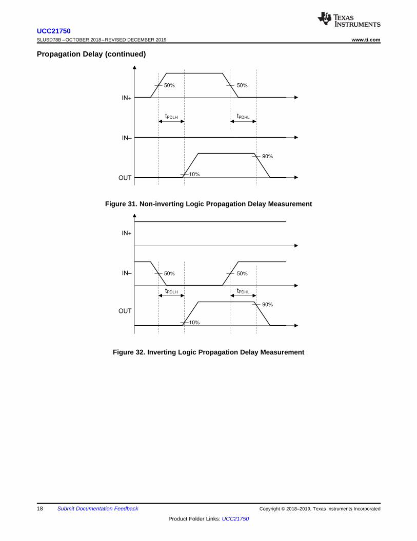
7.1 Propagation Delay
7.1.1 Regular Turn-OFFFigure 31 shows the propagation delay measurement for non-inverting configurations. Figure 32 shows thepropagation delay measurement with the inverting configurations.
tPDLH
IN+
,1Å
tPDHL
50%
10%
90%
OUT
50%
tPDLH
IN+
,1Å
tPDHL
50%
10%
90%
OUT
50%
18
UCC21750SLUSD78B –OCTOBER 2018–REVISED DECEMBER 2019 www.ti.com
Product Folder Links: UCC21750
Submit Documentation Feedback Copyright © 2018–2019, Texas Instruments Incorporated
Propagation Delay (continued)
Figure 31. Non-inverting Logic Propagation Delay Measurement
Figure 32. Inverting Logic Propagation Delay Measurement
IN+
,1Å
OUT
tPWM < TINFIL
IN+
,1Å
OUT
tPWM < TINFIL
IN+
,1Å
OUT
tPWM < TINFIL
IN+
,1Å
OUT
tPWM < TINFIL
19
UCC21750www.ti.com SLUSD78B –OCTOBER 2018–REVISED DECEMBER 2019
Product Folder Links: UCC21750
Submit Documentation FeedbackCopyright © 2018–2019, Texas Instruments Incorporated
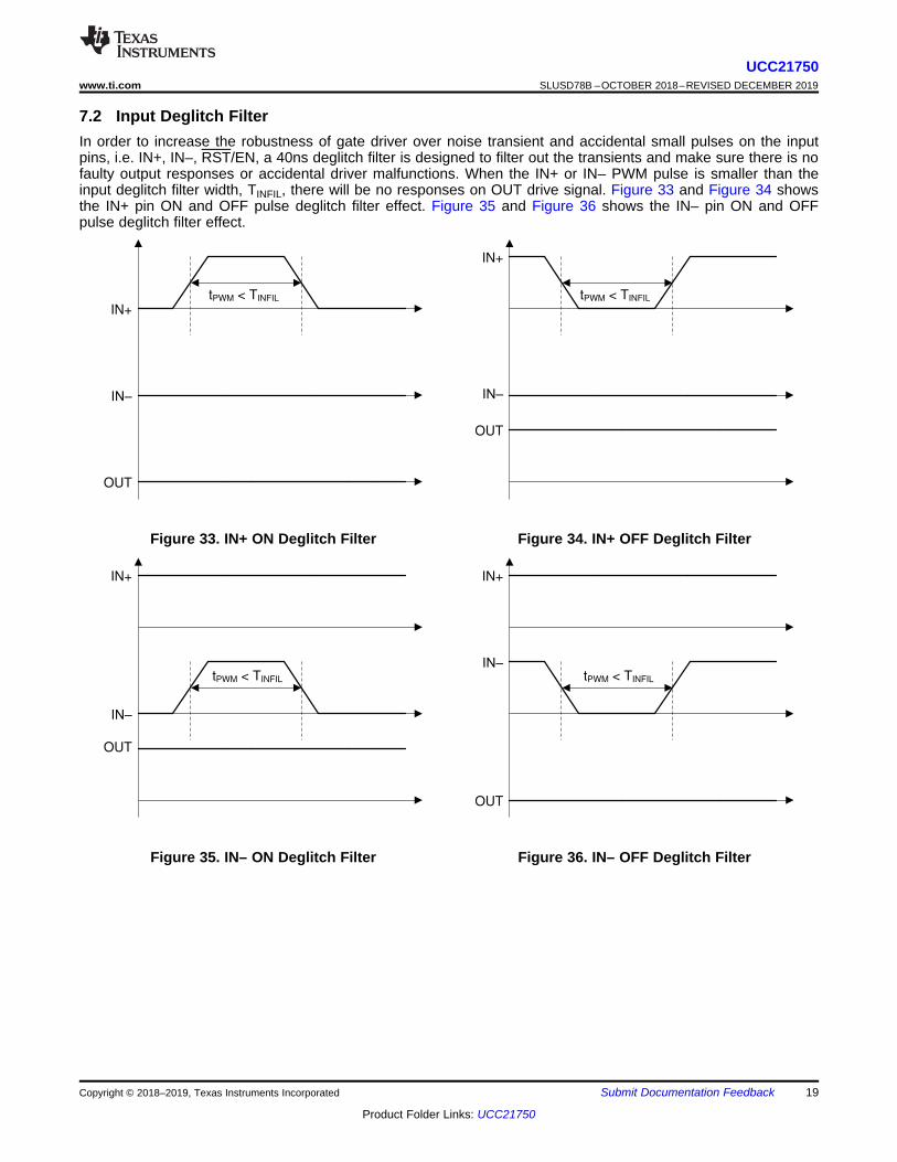
7.2 Input Deglitch FilterIn order to increase the robustness of gate driver over noise transient and accidental small pulses on the inputpins, i.e. IN+, IN–, RST/EN, a 40ns deglitch filter is designed to filter out the transients and make sure there is nofaulty output responses or accidental driver malfunctions. When the IN+ or IN– PWM pulse is smaller than theinput deglitch filter width, TINFIL, there will be no responses on OUT drive signal. Figure 33 and Figure 34 showsthe IN+ pin ON and OFF pulse deglitch filter effect. Figure 35 and Figure 36 shows the IN– pin ON and OFFpulse deglitch filter effect.
Figure 33. IN+ ON Deglitch Filter Figure 34. IN+ OFF Deglitch Filter
Figure 35. IN– ON Deglitch Filter Figure 36. IN– OFF Deglitch Filter

IN(µ,1+¶Åµ,1Ŷ)
OUT
VCLMPTH
CLMPI
Ctrl.
tDCLMPI
LOW
HIGH
20
UCC21750SLUSD78B –OCTOBER 2018–REVISED DECEMBER 2019 www.ti.com
Product Folder Links: UCC21750
Submit Documentation Feedback Copyright © 2018–2019, Texas Instruments Incorporated
7.3 Active Miller Clamp
7.3.1 Internal On-chip Active Miller ClampFor gate driver application with unipolar bias supply or bipolar supply with small negative turn-off voltage, activemiller clamp can help add a additional low impedance path to bypass the miller current and prevent the highdV/dt introduced unintentional turn-on through the miller capacitance. Figure 37 shows the timing diagram for on-chip internal miller clamp function.
Figure 37. Timing Diagram for Internal Active Miller Clamp Function

IN
VCC
VDD
OUT
RDY
APWM
VEE
Hi-Z
tVCC+ to OUT
VVCC_OFF
tVCCFIL
tRDYHLDtVCC+ to RDY t9&&ÅWR5'<
10%
90%
VVCC_ON
(µ,1+¶Åµ,1Ŷ)
COM
t9&&ÅWR287
VCC
VCLMPTH
21
UCC21750www.ti.com SLUSD78B –OCTOBER 2018–REVISED DECEMBER 2019
Product Folder Links: UCC21750
Submit Documentation FeedbackCopyright © 2018–2019, Texas Instruments Incorporated
7.4 Under Voltage Lockout (UVLO)UVLO is one of the key protection features designed to protect the system in case of bias supply failures onVCC — primary side power supply, and VDD — secondary side power supply.
7.4.1 VCC UVLOThe VCC UVLO protection details are discussed in this section. Figure 38 shows the timing diagram illustratingthe definition of UVLO ON/OFF threshold, deglitch filter, response time, RDY and AIN–APWM.
Figure 38. VCC UVLO Protection Timing Diagram

IN
VDD
VEE
OUT
RDY
APWM
COM
Hi-Z
tVDD+ to OUT
VVDD_OFF
tVDDFIL
tRDYHLDtVDD+ to RDY t9''ÅWR5'<
VVDD_ON
(µ,1+¶Åµ,1Ŷ)
10%
VCC
t9''ÅWR287
VCC
VCLMPTH
90%
22
UCC21750SLUSD78B –OCTOBER 2018–REVISED DECEMBER 2019 www.ti.com
Product Folder Links: UCC21750
Submit Documentation Feedback Copyright © 2018–2019, Texas Instruments Incorporated
Under Voltage Lockout (UVLO) (continued)7.4.2 VDD UVLOThe VDD UVLO protection details are discussed in this section. Figure 39 shows the timing diagram illustratingthe definition of UVLO ON/OFF threshold, deglitch filter, response time, RDY and AIN–APWM.
Figure 39. VDD UVLO Protection Timing Diagram

IN(µ,1+¶Åµ,1Ŷ)
DESAT
tDESATLEB
VDESAT
tDESATFIL
VCLMPTH
tDESATOFF
GATE
FLT
tDESATFLT
RST/EN
tDESATLEB
tFLTMUTE
tRSTFILtRSTFIL
90%
OUTH
OUTL
Hi-Z
HIGH
LOW
LOW
Hi-Z
Hi-Z
23
UCC21750www.ti.com SLUSD78B –OCTOBER 2018–REVISED DECEMBER 2019
Product Folder Links: UCC21750
Submit Documentation FeedbackCopyright © 2018–2019, Texas Instruments Incorporated
7.5 Desaturation (DESAT) Protection
7.5.1 DESAT Protection with Soft Turn-OFFDESAT function is used to detect VDS for SiC-MOSFETs or VCE for IGBTs under over current conditions.Figure 40 shows the timing diagram of DESAT operation with soft turn-off during the turning on transition.
Figure 40. DESAT Protection with Soft Turn-OFF During Turn-on Transition
IN(µ,1+¶Åµ,1Ŷ)
DESAT
VDESAT
tDESATFIL
VCLMPTH
tDESATOFF
GATE
FLT
tDESATFLT
RST/EN
tDESATLEB
tFLTMUTE
tRSTFILtRSTFIL
90%
OUTH
OUTL
Hi-Z
HIGH
LOW
LOW
Hi-Z
Hi-Z
24
UCC21750SLUSD78B –OCTOBER 2018–REVISED DECEMBER 2019 www.ti.com
Product Folder Links: UCC21750
Submit Documentation Feedback Copyright © 2018–2019, Texas Instruments Incorporated
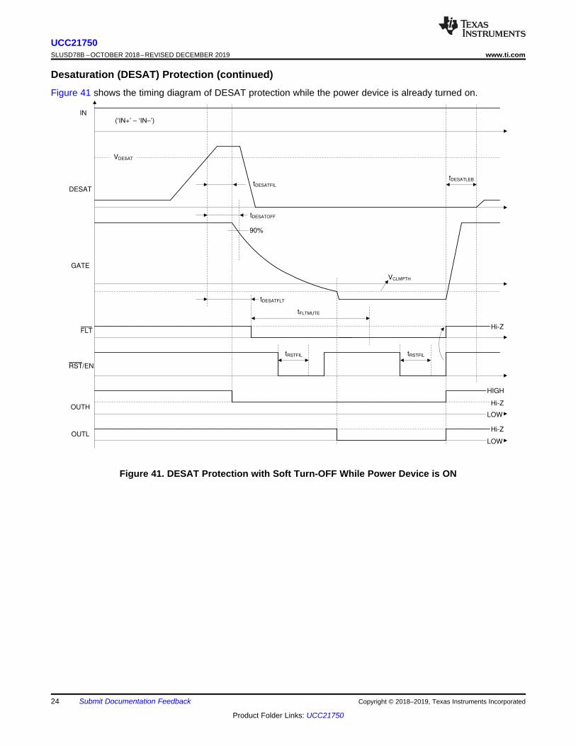
Desaturation (DESAT) Protection (continued)Figure 41 shows the timing diagram of DESAT protection while the power device is already turned on.
Figure 41. DESAT Protection with Soft Turn-OFF While Power Device is ON

25
UCC21750www.ti.com SLUSD78B –OCTOBER 2018–REVISED DECEMBER 2019
Product Folder Links: UCC21750
Submit Documentation FeedbackCopyright © 2018–2019, Texas Instruments Incorporated
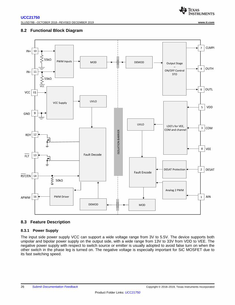
8 Detailed Description
8.1 OverviewThe UCC21750 device is an advanced isolated gate driver with state-of-art protection and sensing features forSiC MOSFETs and IGBTs. The device can support up to 2121V DC operating voltage based on SiC MOSFETsand IGBTs, and can be used to above 10kW applications such as HEV/EV traction inverter, motor drive, on-board and off-board battery charger, solar inverter, etc. The galvanic isolation is implemented by the capacitiveisolation technology, which can realize a reliable reinforced isolation between the low voltage DSP/MCU and highvoltage side.
The ±10A peak sink and source current of UCC21750 can drive the SiC MOSFET modules and IGBT modulesdirectly without an extra buffer. The driver can also be used to drive higher power modules or parallel moduleswith external buffer stage. The input side is isolated with the output side with a reinforced isolation barrier basedon capacitive isolation technology. The device can support up to 1.5-kVRMS working voltage, 12.8-kVPK surgeimmunity with longer than 40 years isolation barrier life. The strong drive strength helps to switch the device fastand reduce the switching loss. While the 150V/ns minimum CMTI guarantees the reliability of the system withfast switching speed. The small propagation delay and part-to-part skew can minimize the deadtime setting, sothe conduction loss can be reduced.
The device includes extensive protection and monitor features to increase the reliability and robustness of theSiC MOSFET and IGBT based systems. The 12V output side power supply UVLO is suitable for switches withgate voltage ≥ 15V. The active miller clamp feature prevents the false turn on causing by miller capacitanceduring fast switching. The device has the state-of-art DESAT detection time, and fault reporting function to thelow voltage side DSP/MCU. The soft turn off is triggered when the DESAT fault is detected, minimizing the shortcircuit energy while reducing the overshoot voltage on the switches.
The isolated analog to PWM sensor can be used as switch temperature sensing, DC bus voltage sensing,auxiliary power supply sensing, etc. The PWM signal can be fed directly to DSP/MCU or through a low-pass-filteras an analog signal.
IN+
VCC
RDY
OUTH
OUTL
APWM
VDD
INt
GND
DEMOD
PWM Driver
15
9
10
11
12
13
14
16
5
3
8
7
4
6
2
1
ISO
LAT
ION
BA
RR
IER
VCC Supply
PWM Inputs MOD
Fault Decode
Fault Encode
LDO[s for VEE,
COM and channel
Analog 2 PWM
Output Stage
t
ON/OFF Control
STO
DESAT Protection
UVLO
UVLO
MODDEMOD
FLT
RST/EN
VCC
COM
CLMPI
VEE
DESAT
AIN
50kQ
55kQ
55kQ
26
UCC21750SLUSD78B –OCTOBER 2018–REVISED DECEMBER 2019 www.ti.com
Product Folder Links: UCC21750
Submit Documentation Feedback Copyright © 2018–2019, Texas Instruments Incorporated
8.2 Functional Block Diagram
8.3 Feature Description
8.3.1 Power SupplyThe input side power supply VCC can support a wide voltage range from 3V to 5.5V. The device supports bothunipolar and bipolar power supply on the output side, with a wide range from 13V to 33V from VDD to VEE. Thenegative power supply with respect to switch source or emitter is usually adopted to avoid false turn on when theother switch in the phase leg is turned on. The negative voltage is especially important for SiC MOSFET due toits fast switching speed.

VDD
ROH
RNMOS
Anti Shoot-
through
Circuitry
ROL
OUTH
OUTL
Input
Signal
Iso
lati
on
Ba
rrie
r
27
UCC21750www.ti.com SLUSD78B –OCTOBER 2018–REVISED DECEMBER 2019
Product Folder Links: UCC21750
Submit Documentation FeedbackCopyright © 2018–2019, Texas Instruments Incorporated
Feature Description (continued)8.3.2 Driver StageUCC21750 has ±10A peak drive strength and is suitable for high power applications. The high drive strength candrive a SiC MOSFET module, IGBT module or paralleled discrete devices directly without extra buffer stage.UCC21750 can also be used to drive higher power modules or parallel modules with extra buffer stage.Regardless of the values of VDD, the peak sink and source current can be kept at 10A. The driver features animportant safety function wherein, when the input pins are in floating condition, the OUTH/OUTL is held in LOWstate. The split output of the driver stage is depicted in Figure 42. The driver has rail-to-rail output byimplementing a hybrid pull-up structure with a P-Channel MOSFET in parallel with an N-Channel MOSFET, andan N-Channel MOSFET to pulldown. The pull-up NMOS is the same as the pull down NMOS, so the onresistance RNMOS is the same as ROL. The hybrid pull-up structure delivers the highest peak-source current whenit is most needed, during the miller plateau region of the power semiconductor turn-on transient. The ROH inrepresents the on-resistance of the pull-up P-Channel MOSFET. However, the effective pull-up resistance ismuch smaller than ROH. Since the pull-up N-Channel MOSFET has much smaller on-resistance than the P-Channel MOSFET, the pull-up N-Channel MOSFET dominates most of the turn-on transient, until the voltage onOUTH pin is about 3V below VDD voltage. The effective resistance of the hybrid pull-up structure during thisperiod is about 2 x ROL . Then the P-Channel MOSFET pulls up the OUTH voltage to VDD rail. The low pull-upimpedance results in strong drive strength during the turn-on transient, which shortens the charging time of theinput capacitance of the power semiconductor and reduces the turn on switching loss.
The pull-down structure of the driver stage is implemented solely by a pull-down N-Channel MOSFET. The on-resistance of the N-Channel MOSFET ROL can be found in the . This MOSFET can ensure the OUTL voltage bepulled down to VEE rail. The low pull-down impedance not only results in high sink current to reduce the turn-offtime, but also helps to increase the noise immunity considering the miller effect.
Figure 42. Gate Driver Output Stage

COM
VEE
OUTL
Control
Circuit
VDD
Ra
28
UCC21750SLUSD78B –OCTOBER 2018–REVISED DECEMBER 2019 www.ti.com
Product Folder Links: UCC21750
Submit Documentation Feedback Copyright © 2018–2019, Texas Instruments Incorporated
Feature Description (continued)8.3.3 VCC and VDD Undervoltage Lockout (UVLO)UCC21750 implements the internal UVLO protection feature for both input and output power supplies VCC andVDD. When the supply voltage is lower than the threshold voltage, the driver output is held as LOW. The outputonly goes HIGH when both VCC and VDD are out of the UVLO status. The UVLO protection feature not onlyreduces the power consumption of the driver itself during low power supply voltage condition, but also increasesthe efficiency of the power stage. For SiC MOSFET and IGBT, the on-resistance reduces while the gate-sourcevoltage or gate-emitter voltage increases. If the power semiconductor is turned on with a low VDD value, theconduction loss increases significantly and can lead to a thermal issue and efficiency reduction of the powerstage. UCC21750 implements 12V threshold voltage of VDD UVLO, with 800mV hysteresis. This thresholdvoltage is suitable for both SiC MOSFET and IGBT.
The UVLO protection block features with hysteresis and deglitch filter, which help to improve the noise immunityof the power supply. During the turn on and turn off switching transient, the driver sources and sinks a peaktransient current from the power supply, which can result in sudden voltage drop of the power supply. Withhysteresis and UVLO deglitch filter, the internal UVLO protection block will ignore small noises during the normalswitching transients.
The timing diagrams of the UVLO feature of VCC and VDD are shown in Figure 38, and Figure 39. The RDY pinon the input side is used to indicate the power good condition. The RDY pin is open drain. During UVLOcondition, the RDY pin is held in low status and connected to GND. Normally the pin is pulled up externally toVCC to indicate the power good. The AIN-APWM function stops working during the UVLO status. The APWM pinon the input side will be held LOW.
8.3.4 Active PulldownUCC21750 implements an active pulldown feature to ensure the OUTH/OUTL pin clamping to VEE when theVDD is open. The OUTH/OUTL pin is in high-impedance status when VDD is open, the active pulldown featurecan prevent the output be false turned on before the device is back to control.
Figure 43. Active Pulldown
8.3.5 Short Circuit ClampingDuring short circuit condition, the miller capacitance can cause a current sinking to the OUTH/OUTL/CLMPI pindue to the high dV/dt and boost the OUTH/OUTL/CLMPI voltage. The short circuit clamping feature ofUCC21750 can clamp the OUTH/OUTL/CLMPI pin voltage to be slightly higher than VDD, which can protect thepower semiconductors from a gate-source and gate-emitter overvoltage breakdown. This feature is realized byan internal diode from the OUTH/OUTL/CLMPI to VDD.

Isola
tion b
arr
ier
IN+
µC
VCC
IN-
+
±
3V to 5.5V
MOD
VCC
OUTH
COM
VEE
VCLMPTH
Control
Circuitry
CLMPI
OUTL
DEMOD
VDD
Control Circuitry
OUTH
OUTL
D1 D2 D3
CLMPI
29
UCC21750www.ti.com SLUSD78B –OCTOBER 2018–REVISED DECEMBER 2019
Product Folder Links: UCC21750
Submit Documentation FeedbackCopyright © 2018–2019, Texas Instruments Incorporated
Feature Description (continued)
Figure 44. Short Circuit Clamping
8.3.6 Internal Active Miller ClampActive miller clamp feature is important to prevent the false turn-on while the driver is in OFF state. Inapplications which the device can be in synchronous rectifier mode, the body diode conducts the current duringthe deadtime while the device is in OFF state, the drain-source or collector-emitter voltage remains the same andthe dV/dt happens when the other power semiconductor of the phase leg turns on. The low internal pull-downimpedance of UCC21750 can provide a strong pulldown to hold the OUTL to VEE. However, external gateresistance is usually adopted to limit the dV/dt. The miller effect during the turn on transient of the other powersemiconductor can cause a voltage drop on the external gate resistor, which boost the gate-source or gate-emitter voltage. If the voltage on VGS or VGE is higher than the threshold voltage of the power semiconductor, ashoot through can happen and cause catastrophic damage. The active miller clamp feature of UCC21750 drivesan internal MOSFET, which connects to the device gate. The MOSFET is triggered when the gate voltage islower than VCLMPTH, which is 2V above VEE, and creates a low impedance path to avoid the false turn on issue.
Figure 45. Active Miller Clamp

+
+
±
COM
DESAT
VDD
CBLK
DHVR
DESAT Fault
Control Logic
VDESAT
15
0n
s
Deg
litc
h F
ilte
r
30
UCC21750SLUSD78B –OCTOBER 2018–REVISED DECEMBER 2019 www.ti.com
Product Folder Links: UCC21750
Submit Documentation Feedback Copyright © 2018–2019, Texas Instruments Incorporated
Feature Description (continued)8.3.7 Desaturation (DESAT) ProtectionThe UCC21750 implements a fast overcurrent and short circuit protection feature to protect the IGBT modulefrom catastrophic breakdown during fault. The DESAT pin of the device has a typical 9V threshold with respect toCOM, source or emitter of the power semiconductor. When the input is in floating condition, or the output is heldin low state, the DESAT pin is pulled down by an internal MOSFET and held in LOW state, which prevents theovercurrent and short circuit fault from false triggering. The internal current source of the DESAT pin is activatedonly during the driver ON state, which means the overcurrent and short circuit protection feature only works whenthe power semiconductor is in on state. The internal pulldown MOSFET helps to discharge the voltage of DESATpin when the power semiconductor is turned off. UCC21750 features a 200ns internal leading edge blanking timeafter the OUTH switches to high state. The internal current source is activated to charge the external blankingcapacitor after the internal leading edge blanking time. The typical value of the internal current source is 500µA.
Figure 46. DESAT Protection
8.3.8 Soft Turn-offUCC21750 initiates a soft turn-off when the overcurrent and short circuit protection is triggered. When theovercurrent and short circuit fault happens, the IGBT transits from the active region to the desaturation regionvery fast. The channel current is controlled by the gate voltage and decreasing in a soft manner, thus theovershoot of the IGBT is limited and prevents the overvoltage breakdown. There is a tradeoff between theovershoot voltage and short circuit energy. The turn off speed needs to be slow to limit the overshoot voltage, butthe shutdown time should not be too long that the large energy dissipation can breakdown the device. The400mA soft turn off current of UCC21750 makes sure the power switches is safely turned off during short circuitevents. The timing diagram of soft turn-off shows in Figure 40.

Soft Turn-off
VEE
OUTL
+
+
±
COM
DESAT
VDD
CBLK
DHVR
Control Logic
VDESAT
15
0n
s
Deg
litc
h F
ilte
r
31
UCC21750www.ti.com SLUSD78B –OCTOBER 2018–REVISED DECEMBER 2019
Product Folder Links: UCC21750
Submit Documentation FeedbackCopyright © 2018–2019, Texas Instruments Incorporated
Feature Description (continued)
Figure 47. Soft Turn-off
8.3.9 Fault (FLT, Reset and Enable (RST/EN)The FLT pin of UCC21750 is open drain and can report a fault signal to the DSP/MCU when the fault is detectedthrough the DESAT pin. The FLT pin will be pulled down to GND after the fault is detected, and is held low until areset signal is received from RST/EN. The device has a fault mute time tFLTMUTE, within which the device ignoresany reset signal.
The RST/EN is pulled down internally by a 50kΩ resistor, and is thus disabled by default when this pin is floating.It must be pulled up externally to enable the driver. The pin has two purposes:• To reset the FLT pin. To reset, then RST/EN pin is pulled low; if the pin is set and held in low state for more
than tRSTFIL after the mute time tFLTMUTE, then the fault signal is reset and FLT is reset back to the highimpedance status at the rising edge of the input signal at RST/EN pin.
• Enable and shutdown the device. If the RST/EN pin is pulled low for longer than tRSTFIL, the driver will bedisabled and OUTL will be activated to pull down the gate of the IGBT or SiC MOSFET. The pin must bepulled up externally to enable the part, otherwise the device is disabled by default.
8.3.10 Isolated Analog to PWM Signal FunctionThe UCC21750 features an isolated analog to PWM signal function from AIN to APWM pin, which allows theisolated temperature sensing, high voltage dc bus voltage sensing, etc. An internal current source IAIN in AIN pinis implemented in the device to bias an external thermal diode or temperature sensing resistor. The UCC21750encodes the voltage signal VAIN to a PWM signal, passing through the reinforced isolation barrier, and output toAPWM pin on the input side. The PWM signal can either be transferred directly to DSP/MCU to calculate theduty cycle, or filtered by a simple RC filter as an analog signal. The AIN voltage input range is from 0.6V to 4.5V,and the corresponding duty cycle of the APWM output ranges from 88% to 10%. The duty cycle increases

COM
VDD
Cfilt
AIN
+
OSC
MOD
In Module or
Discrete
Thermal
Diode
Iso
lation
barr
ier
NTC or
PTC
UCC217xx
DEMOD
APWM
VCC
GND
µC
+
±
3V to 5.5V
+
±
13V to
33V
Rfilt
32
UCC21750SLUSD78B –OCTOBER 2018–REVISED DECEMBER 2019 www.ti.com
Product Folder Links: UCC21750
Submit Documentation Feedback Copyright © 2018–2019, Texas Instruments Incorporated
Feature Description (continued)linearly from 10% to 88% while the AIN voltage decreases from 4.5V to 0.6V. This corresponds to thetemperature coefficient of the negative temperature coefficient (NTC) resistor and thermal diode. When AIN isfloating, the AIN voltage is 5V and the APWM operates at 400kHz with approximately 10% duty cycle. Theaccuracy of the duty cycle is ±3% across temperature without one time calibration. The accuracy can beimproved using calibration. The accuracy of the internal current source IAIN is ±3% across temperature.
The isolated analog to PWM signal feature can also support other analog signal sensing, such as the highvoltage dc bus voltage, etc. The internal current source IAIN should be taken into account when designing thepotential divider if sensing a high voltage.
Figure 48. Isolated Analog to PWM Signal

33
UCC21750www.ti.com SLUSD78B –OCTOBER 2018–REVISED DECEMBER 2019
Product Folder Links: UCC21750
Submit Documentation FeedbackCopyright © 2018–2019, Texas Instruments Incorporated
8.4 Device Functional ModesTable 1 lists the device function.
Table 1. Function TableInput Output
VCC VDD VEE IN+ IN- RST/EN AIN RDY FLT OUTH/OUTL CLMPI APWM
PU PD PU X X X X Low HiZ Low Low LowPD PU PU X X X X HiZ HiZ Low Low LowPU PU PU X X Low X HiZ HiZ Low Low LowPU Open PU X X X X Low HiZ HiZ HiZ HiZPU PU Open X X X X Low HiZ Low Low LowPU PU PU Low X High X HiZ HiZ Low Low P*
PU PU PU X High High X HiZ HiZ Low Low P*
PU PU PU High High High X HiZ HiZ Low Low P*
PU: Power Up (VCC ≥ 2.85V, VDD ≥ 13.1V, VEE ≤ 0V); PD: Power Down (VCC ≤ 2.35V, VDD ≤ 9.9V); X:Irrelevant; P*: PWM Pulse; HiZ: High Impedance

34
UCC21750SLUSD78B –OCTOBER 2018–REVISED DECEMBER 2019 www.ti.com
Product Folder Links: UCC21750
Submit Documentation Feedback Copyright © 2018–2019, Texas Instruments Incorporated
9 Applications and Implementation
NOTEInformation in the following applications sections is not part of the TI componentspecification, and TI does not warrant its accuracy or completeness. TI’s customers areresponsible for determining suitability of components for their purposes. Customers shouldvalidate and test their design implementation to confirm system functionality.
9.1 Application InformationThe UCC21750 device is very versatile because of the strong drive strength, wide range of output power supply,high isolation ratings, high CMTI and superior protection and sensing features. The 1.5-kVRMS working voltageand 12.8-kVPK surge immunity can support up both SiC MOSFET and IGBT modules with DC bus voltage up to2121V. The device can be used in both low power and high power applications such as the traction inverter inHEV/EV, on-board charger and charging pile, motor driver, solar inverter, industrial power supplies and etc. Thedevice can drive the high power SiC MOSFET module, IGBT module or paralleled discrete device directly withoutexternal buffer drive circuit based on NPN/PNP bipolar transistor in totem-pole structure, which allows the driverto have more control to the power semiconductor and saves the cost and space of the board design. UCC21750can also be used to drive very high power modules or paralleled modules with external buffer stage. The inputside can support power supply and microcontroller signal from 3.3V to 5V, and the device level shifts the signalto output side through reinforced isolation barrier. The device has wide output power supply range from 13V to33V and support wide range of negative power supply. This allows the driver to be used in SiC MOSFETapplications, IGBT application and many others. The 12V UVLO benefits the power semiconductor with lowerconduction loss and improves the system efficiency. As a reinforced isolated single channel driver, the devicecan be used to drive either a low-side or high-side driver.
UCC21750 device features extensive protection and monitoring features, which can monitor, report and protectthe system from various fault conditions.• Fast detection and protection for the overcurrent and short circuit fault. The semiconductor is shutdown when
the fault is detected and FLT pin is pulled down to indicate the fault detection. The device is latched unlessreset signal is received from the RST/EN pin.
• Soft turn-off feature to protect the power semiconductor from catastrophic breakdown during overcurrent andshort circuit fault. The shutdown energy can be controlled while the overshoot of the power semiconductor islimited.
• UVLO detection to protect the semiconductor from excessive conduction loss. Once the device is detected tobe in UVLO mode, the output is pulled down and RDY pin indicates the power supply is lost. The device isback to normal operation mode once the power supply is out of the UVLO status. The power good status canbe monitored from the RDY pin.
• Analog signal seensing with isolated analog to PWM signal feature. This feature allows the device to sensethe temperature of the semiconductor from the thermal diode or temperature sensing resistor, or dc busvoltage with resistor divider. A PWM signal is generated on the low voltage side with reinforced isolated fromthe high voltage side. The signal can be fed back to the microcontroller for the temperature monitoring,voltage monitoring and etc.
• The active miller clamp feature protects the power semiconductor from false turn on.• Enable and disable function through the RST/EN pin.• Short circuit clamping.• Active pulldown.
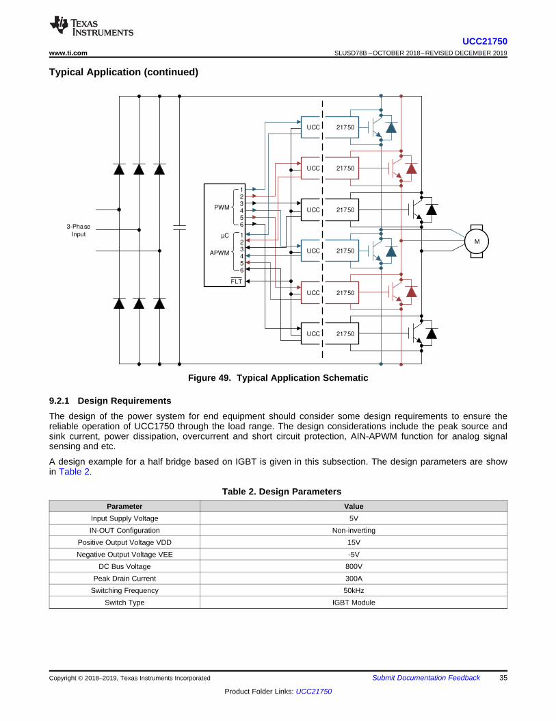
9.2 Typical ApplicationFigure 49 shows the typical application of a half bridge using two UCC21750 isolated gate drivers. The halfbridge is a basic element in various power electronics applications such as in motor drive applications to controlthe operating speed and torque of an AC motor.
µCM
UCC 21750
UCC 21750
UCC 21750
UCC 21750
UCC 21750
UCC 21750
3-Phase
Input
PWM
123456
FLT
123456
APWM
35
UCC21750www.ti.com SLUSD78B –OCTOBER 2018–REVISED DECEMBER 2019
Product Folder Links: UCC21750
Submit Documentation FeedbackCopyright © 2018–2019, Texas Instruments Incorporated
Typical Application (continued)
Figure 49. Typical Application Schematic
9.2.1 Design RequirementsThe design of the power system for end equipment should consider some design requirements to ensure thereliable operation of UCC1750 through the load range. The design considerations include the peak source andsink current, power dissipation, overcurrent and short circuit protection, AIN-APWM function for analog signalsensing and etc.
A design example for a half bridge based on IGBT is given in this subsection. The design parameters are showin Table 2.
Table 2. Design ParametersParameter Value
Input Supply Voltage 5VIN-OUT Configuration Non-inverting
Positive Output Voltage VDD 15VNegative Output Voltage VEE -5V
DC Bus Voltage 800VPeak Drain Current 300A
Switching Frequency 50kHzSwitch Type IGBT Module

Microcontroller
PWM_T
PWM_B
IN+
IN-
IN+
IN-
OUTH
OUTL
RON
ROFF
OUTH
OUTL
RON
ROFF
36
UCC21750SLUSD78B –OCTOBER 2018–REVISED DECEMBER 2019 www.ti.com
Product Folder Links: UCC21750
Submit Documentation Feedback Copyright © 2018–2019, Texas Instruments Incorporated
9.2.2 Detailed Design Procedure
9.2.2.1 Input filters for IN+, IN- and RST/ENIn the applications of traction inverter or motor drive, the power semiconductors are in hard switching mode. Withthe strong drive strength of UCC21750, the dV/dt can be high, especially for SiC MOSFET. Noise can not onlybe coupled to the gate voltage due to the parasitic inductance, but also to the input side as the non-ideal PCBlayout and coupled capacitance.
UCC21750 features a 40ns internal deglitch filter to IN+, IN- and RST/EN pin. Any signal less than 40ns can befiltered out from the input pins. For noisy systems, external low pass filter can be added externally to the inputpins. Adding low pass filters to IN+, IN- and RST/EN pins can effectively increase the noise immunity andincrease the signal integrity. When not in use, the IN+, IN- and RST/EN pins should not be floating. IN- should betied to GND if only IN+ is used for non-inverting input to output configuration. The purpose of the low pass filter isto filter out the high frequency noise generated by the layout parasitics. While choosing the low pass filterresistors and capacitors, both the noise immunity effect and delay time should be considered according to thesystem requirements.
9.2.2.2 PWM Interlock of IN+ and IN-UCC21750 features the PWM interlock for IN+ and IN- pins, which can be used to prevent the phase leg shootthrough issue. As shown in Table 1, the output is logic low while both IN+ and IN- are logic high. When only IN+is used, IN- can be tied to GND. To utilize the PWM interlock function, the PWM signal of the other switch in thephase leg can be sent to the IN- pin. As shown in Figure 50, the PWM_T is the PWM signal to top side switch,the PWM_B is the PWM signal to bottom side switch. For the top side gate driver, the PWM_T signal is given tothe IN+ pin, while the PWM_B signal is given to the IN- pin; for the bottom side gate driver, the PWM_B signal isgiven to the IN+ pin, while PWM_T signal is given to the IN- pin. When both PWM_T and PWM_B signals arehigh, the outputs of both gate drivers are logic low to prevent the shoot through condition.
Figure 50. PWM Interlock for a Half Bridge
9.2.2.3 FLT, RDY and RST/EN Pin CircuitryBoth FLT and RDY pin are open-drain output. The RST/EN pin has 50kΩ internal pulldown resistor, so the driveris in OFF status if the RST/EN pin is not pulled up externally. A 5kΩ resistor can be used as pullup resistor forthe FLT, RDY and RST/EN pins.
To improve the noise immunity due to the parasitic coupling and common mode noise, low pass filters can beadded between the FLT, RDY and RST/EN pins and the microcontroller. A filter capacitor between 100pF to300pF can be added.

IN+
VCC
FLT
RDY
RST/EN
APWM
INt
GNDM
icro
-co
ntr
olle
r
(MC
U)
16
15
14
13
12
11
3.3V to 5V
0.1µF 1µF
9
5kQ 5kQ
100pF
100pF
100pF
5kQ
10
37
UCC21750www.ti.com SLUSD78B –OCTOBER 2018–REVISED DECEMBER 2019
Product Folder Links: UCC21750
Submit Documentation FeedbackCopyright © 2018–2019, Texas Instruments Incorporated
Figure 51. FLT, RDY and RST/EN Pins Circuitry
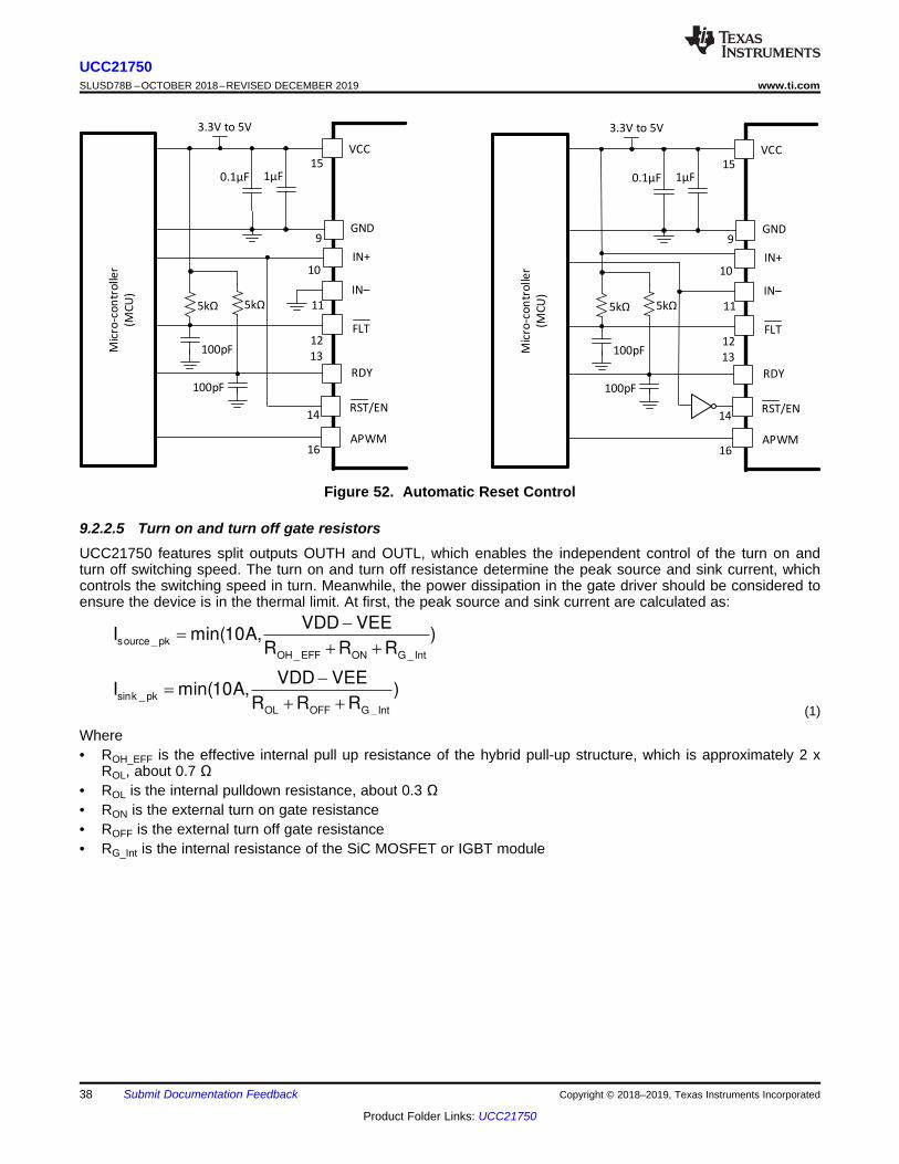
9.2.2.4 RST/EN Pin ControlRST/EN pin has two functions. It is used to enable or shutdown the outputs of the driver and to reset the faultsignaled on the FLT pin after DESAT is detected. RST/EN pin needs to be pulled up to enable the device; whenthe pin is pulled down, the device is in disabled status. By default the driver is disabled with the internal 50kΩpulldown resistor at this pin.
When the driver is latched after DESAT is detected, the FLT pin and output are latched low and need to be resetby the RST/EN pin. The microcontroller must send a signal to RST/EN pin after the fault to reset the driver. Thedriver will not respond until after the mute time tFLTMUTE. The reset signal must be held low for at least tRSTFIL afterthe mute time.
This pin can also be used to automatically reset the driver. The continuous input signal IN+ or IN- can be appliedto RST/EN pin. There is no separate reset signal from the microcontroller when configuring the driver this way. Ifthe PWM is applied to the non-inverting input IN+, then IN+ can also be tied to RST/EN pin. If the PWM isapplied to the inverting input IN-, then a NOT logic is needed between the PWM signal from the microcontrollerand the RST/EN pin. Using either configuration results in the driver being reset in every switching cycle withoutan extra control signal from microcontroller tied to RST/EN pin. One must ensure the PWM off-time is greaterthan tRSTFIL in order to reset the driver in cause of a DESAT fault.
source _ pk
OH _EFF ON G _Int
sink _ pk
OL OFF G _Int
VDD VEEI min(10A, )
R R R
VDD VEEI min(10A, )
R R R
IN+
VCC
FLT
RDY
RST/EN
APWM
INt
GND
Mic
ro-c
on
tro
ller
(MC
U)
16
15
14
13
12
11
3.3V to 5V
0.1µF 1µF
9
5kQ 5kQ
100pF
100pF
10IN+
VCC
FLT
RDY
RST/EN
APWM
INt
GND
Mic
ro-c
on
tro
ller
(MC
U)
16
15
14
13
12
11
3.3V to 5V
0.1µF 1µF
9
5kQ 5kQ
100pF
100pF
10
38
UCC21750SLUSD78B –OCTOBER 2018–REVISED DECEMBER 2019 www.ti.com
Product Folder Links: UCC21750
Submit Documentation Feedback Copyright © 2018–2019, Texas Instruments Incorporated
Figure 52. Automatic Reset Control
9.2.2.5 Turn on and turn off gate resistorsUCC21750 features split outputs OUTH and OUTL, which enables the independent control of the turn on andturn off switching speed. The turn on and turn off resistance determine the peak source and sink current, whichcontrols the switching speed in turn. Meanwhile, the power dissipation in the gate driver should be considered toensure the device is in the thermal limit. At first, the peak source and sink current are calculated as:
(1)
Where• ROH_EFF is the effective internal pull up resistance of the hybrid pull-up structure, which is approximately 2 x
ROL, about 0.7 Ω• ROL is the internal pulldown resistance, about 0.3 Ω• RON is the external turn on gate resistance• ROFF is the external turn off gate resistance• RG_Int is the internal resistance of the SiC MOSFET or IGBT module

ce stray load OFF OL G_Int ies plat thV L I / ((R R R ) C ln(V / V ))'
source _ pk
OH _ EFF ON G _Int
sink _ pk
OL OFF G _Int
VDD VEEI min(10A, ) 5.9A
R R R
VDD VEEI min(10A, ) 6.7A
R R R
|
|
RONOUTH
OUTL
VEE
Cgc
Cge
Cies=Cgc+Cge
VDD
+
tVDD
+
t
VEE
ROFF
RG_Int
ROH_EFF
ROL
COM
39
UCC21750www.ti.com SLUSD78B –OCTOBER 2018–REVISED DECEMBER 2019
Product Folder Links: UCC21750
Submit Documentation FeedbackCopyright © 2018–2019, Texas Instruments Incorporated
Figure 53. Output Model for Calculating Peak Gate Current
For example, for an IGBT module based system with the following parameters:• Qg = 3300 nC• RG_Int = 1.7 Ω• RON=ROFF= 1 Ω
The peak source and sink current in this case are:
(2)
Thus by using 1Ω external gate resistance, the peak source current is 5.9A, the peak sink current is 6.7A. Thecollector-to-emitter dV/dt during the turn on switching transient is dominated by the gate current at the millerplateau voltage. The hybrid pullup structure ensures the peak source current at the miller plateau voltage, unlessthe turn on gate resistor is too high. The faster the collector-to-emitter, Vce, voltage rises to VDC, the smaller theturn on switching loss is. The dV/dt can be estimated as Qgc/Isource_pk. For the turn off switching transient, thedrain-to-source dV/dt is dominated by the load current, unless the turn off gate resistor is too high. After Vcereaches the dc bus voltage, the power semiconductor is in saturation mode and the channel current is controlledby Vge. The peak sink current determines the dI/dt, which dominates the Vce voltage overshoot accordingly. Ifusing relatively large turn off gate resistance, the Vce overshoot can be limited. The overshoot can be estimatedby:
(3)
Where• Lstray is the stray inductance in power switching loop, as shown in Figure 54• Iload is the load current, which is the turn off current of the power semiconductor• Cies is the input capacitance of the power semiconductor• Vplat is the plateau voltage of the power semiconductor• Vth is the threshold voltage of the power semiconductor
OH _ EFF OLSW sw g
OH _ EFF ON G _Int OL OFF G _Int
R R1P ( ) (VDD VEE) f Q 0.505W
2 R R R R R R
OH _EFF OLSW sw g
OH _EFF ON G _Int OL OFF G _Int
R R1P ( ) (VDD VEE) f Q
2 R R R R R R
DR Q SWP P P
RG
RG
+
t
+
t
OUTH
OUTL
Lload
Lstray=LDC+Le1+Lc1+Le1+Lc1
COM
VDC
Cgc
Cge
Cies=Cgc+Cge
VDD
LDC
Lc1
Le1
Lc2
Le2
40
UCC21750SLUSD78B –OCTOBER 2018–REVISED DECEMBER 2019 www.ti.com
Product Folder Links: UCC21750
Submit Documentation Feedback Copyright © 2018–2019, Texas Instruments Incorporated
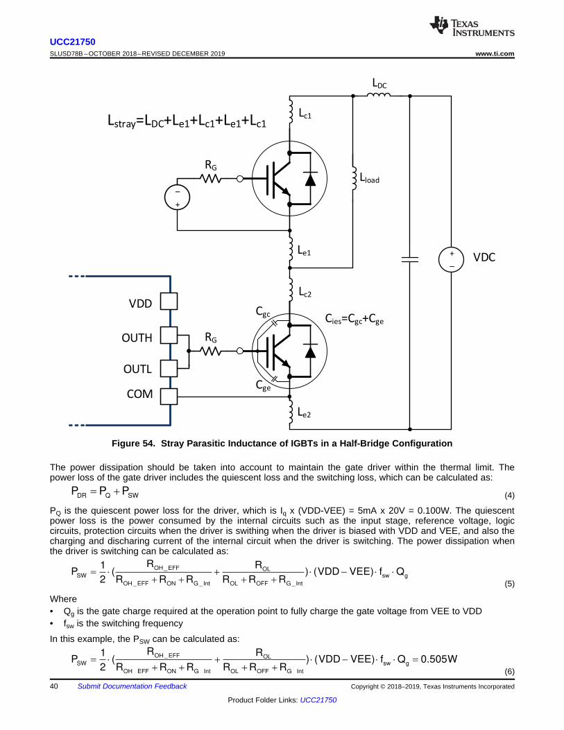
Figure 54. Stray Parasitic Inductance of IGBTs in a Half-Bridge Configuration
The power dissipation should be taken into account to maintain the gate driver within the thermal limit. Thepower loss of the gate driver includes the quiescent loss and the switching loss, which can be calculated as:
(4)
PQ is the quiescent power loss for the driver, which is Iq x (VDD-VEE) = 5mA x 20V = 0.100W. The quiescentpower loss is the power consumed by the internal circuits such as the input stage, reference voltage, logiccircuits, protection circuits when the driver is swithing when the driver is biased with VDD and VEE, and also thecharging and discharing current of the internal circuit when the driver is switching. The power dissipation whenthe driver is switching can be calculated as:
(5)
Where• Qg is the gate charge required at the operation point to fully charge the gate voltage from VEE to VDD• fsw is the switching frequency
In this example, the PSW can be calculated as:
(6)

APWM AIND (%) 20 * V 100
o
j b jb DRT T P 150 C \ |
DR Q SWP P P 0.10W 0.505W 0.605W
41
UCC21750www.ti.com SLUSD78B –OCTOBER 2018–REVISED DECEMBER 2019
Product Folder Links: UCC21750
Submit Documentation FeedbackCopyright © 2018–2019, Texas Instruments Incorporated
Thus, the total power loss is:
(7)
When the board temperature is 125°C, the junction temperature can be estimated as:
(8)
Therefore, for the application in this example, with 125°C board temperature, the maximum switching frequencyis ~50kHz to keep the gate driver in the thermal limit. By using a lower switching frequency, or increasingexternal gate resistance, the gate driver can be operated at a higher switching frequency.
9.2.2.6 Overcurrent and Short Circuit ProtectionA standard desaturation circuit can be applied to the DESAT pin. If the voltage of the DESAT pin is higher thanthe threshold VDESAT, the soft turn-off is initiated. A fault will be reported to the input side to DSP/MCU. Theoutput is held to LOW after the fault is detected, and can only be reset by the RST/EN pin. The state-of-artovercurrent and short circuit detection time helps to ensure a short shutdown time for SiC MOSFET and IGBT.
If DESAT pin is not in use, it must be tied to COM to avoid overcurrent fault false triggering.• Fast reverse recovery high voltage diode is recommended in the desaturation circuit. A resistor is
recommended in series with the high voltage diode to limit the inrush current.• A Schottky diode is recommended from COM to DESAT to prevent driver damage caused by negative
voltage.• A Zener diode is recommended from COM to DESAT to prevent driver damage caused by positive voltage.
9.2.2.7 Isolated Analog Signal SensingThe isolated analog signal sensing feature provides a simple isolated channel for the isolated temperaturedetection, voltage sensing and etc. One typical application of this function is the temperature monitor of thepower semiconductor. Thermal diodes or temperature sensing resistors are integrated in the SiC MOSFET orIGBT module close to the dies to monitor the junction temperature. UCC21750 has an internal 200uA currentsource with ±3% accuracy across temperature, which can forward bias the thermal diodes or create a voltagedrop on the temperature sensing resistors. The sensed voltage from the AIN pin is passed through the isolationbarrier to the input side and transformed to a PWM signal. The duty cycle of the PWM changes linearly from 10%to 88% when the AIN voltage changes from 4.5V to 0.6V and can be represented using Equation 9.
(9)
9.2.2.7.1 Isolated Temperature Sensing
A typical application circuit is shown in Figure 55. To sense temperature, the AIN pin is connected to the thermaldiode or thermistor which can be discrete or integrated within the power module. A low pass filter isrecommended for the AIN input. Since the temperature signal does not have a high bandwidth, the low pass filteris mainly used for filtering the noise introduced by the switching of the power device, which does not requirestringent control for propagation delay. The filter capacitance for Cfilt can be chosen between 1nF to 100nF andthe filter resistance Rfilt between 1Ω to 10Ω according to the noise level.
The output of APWM is directly connected to the microcontroller to measure the duty cycle dependent on thevoltage input at AIN, using Equation 9.
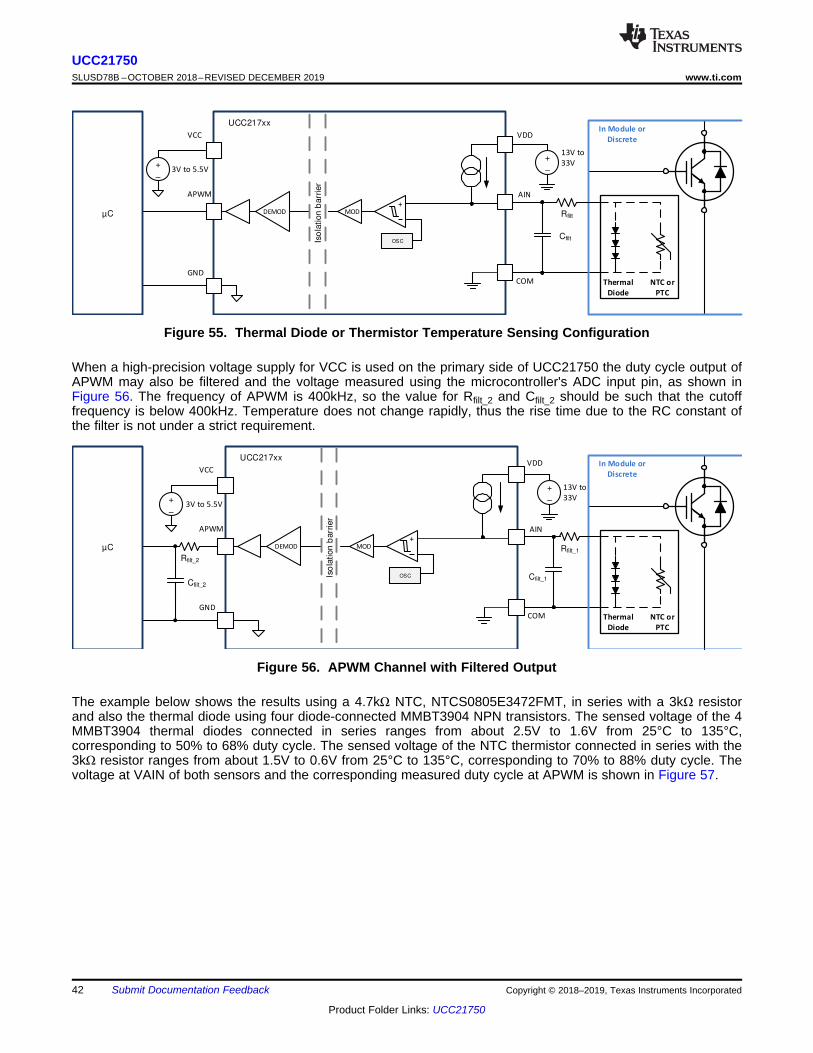
COM
VDD
Cfilt_1
AIN
+
OSC
MOD
In Module or
Discrete
Thermal
Diode
Iso
lation
barr
ier
NTC or
PTC
UCC217xx
DEMOD
APWM
Rfilt_2
Cfilt_2
µC
VCC
GND
+
±
3V to 5.5V
+
±
13V to
33V
Rfilt_1
COM
VDD
Cfilt
AIN
+
OSC
MOD
In Module or
Discrete
Thermal
Diode
Iso
lation
barr
ier
NTC or
PTC
UCC217xx
DEMOD
APWM
VCC
GND
µC
+
±
3V to 5.5V
+
±
13V to
33V
Rfilt
42
UCC21750SLUSD78B –OCTOBER 2018–REVISED DECEMBER 2019 www.ti.com
Product Folder Links: UCC21750
Submit Documentation Feedback Copyright © 2018–2019, Texas Instruments Incorporated
Figure 55. Thermal Diode or Thermistor Temperature Sensing Configuration
When a high-precision voltage supply for VCC is used on the primary side of UCC21750 the duty cycle output ofAPWM may also be filtered and the voltage measured using the microcontroller's ADC input pin, as shown inFigure 56. The frequency of APWM is 400kHz, so the value for Rfilt_2 and Cfilt_2 should be such that the cutofffrequency is below 400kHz. Temperature does not change rapidly, thus the rise time due to the RC constant ofthe filter is not under a strict requirement.
Figure 56. APWM Channel with Filtered Output
The example below shows the results using a 4.7kΩ NTC, NTCS0805E3472FMT, in series with a 3kΩ resistorand also the thermal diode using four diode-connected MMBT3904 NPN transistors. The sensed voltage of the 4MMBT3904 thermal diodes connected in series ranges from about 2.5V to 1.6V from 25°C to 135°C,corresponding to 50% to 68% duty cycle. The sensed voltage of the NTC thermistor connected in series with the3kΩ resistor ranges from about 1.5V to 0.6V from 25°C to 135°C, corresponding to 70% to 88% duty cycle. Thevoltage at VAIN of both sensors and the corresponding measured duty cycle at APWM is shown in Figure 57.
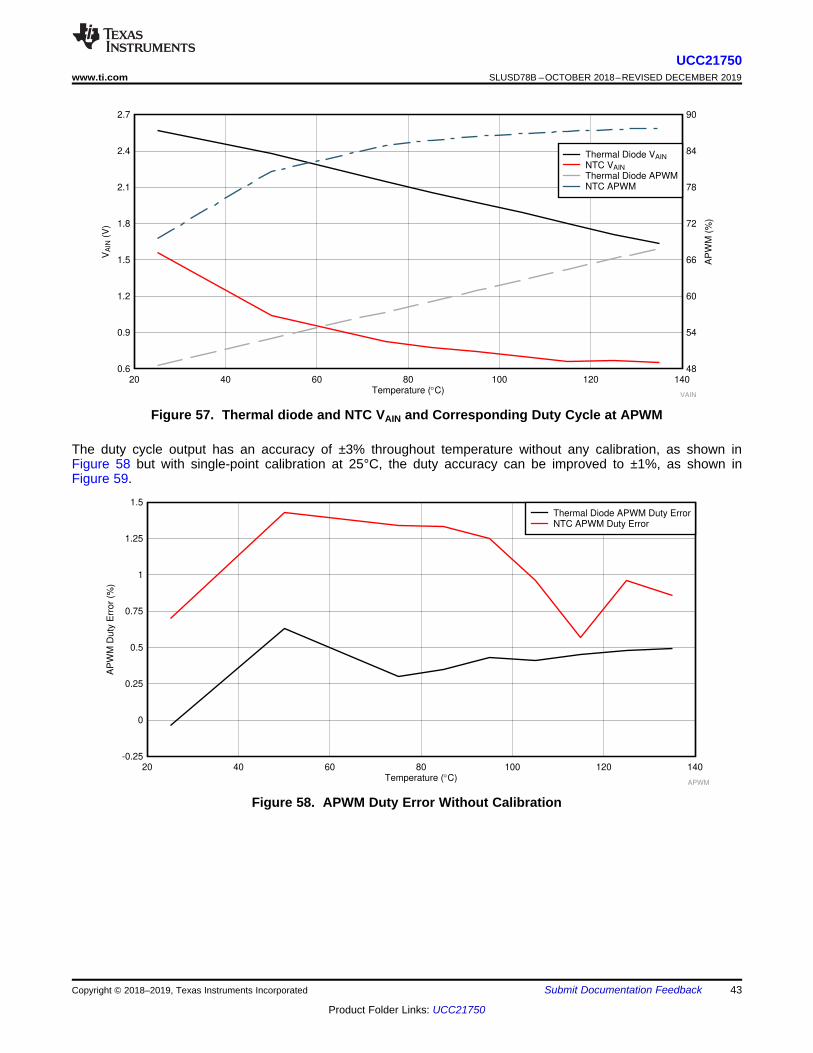
Temperature (qC)
AP
WM
Du
ty E
rror
(%)
20 40 60 80 100 120 140-0.25
0
0.25
0.5
0.75
1
1.25
1.5
APWM
Thermal Diode APWM Duty ErrorNTC APWM Duty Error
Temperature (qC)
VA
IN (
V)
AP
WM
(%
)
20 40 60 80 100 120 1400.6 48
0.9 54
1.2 60
1.5 66
1.8 72
2.1 78
2.4 84
2.7 90
VAIN
Thermal Diode VAIN
NTC VAIN
Thermal Diode APWMNTC APWM
43
UCC21750www.ti.com SLUSD78B –OCTOBER 2018–REVISED DECEMBER 2019
Product Folder Links: UCC21750
Submit Documentation FeedbackCopyright © 2018–2019, Texas Instruments Incorporated
Figure 57. Thermal diode and NTC VAIN and Corresponding Duty Cycle at APWM
The duty cycle output has an accuracy of ±3% throughout temperature without any calibration, as shown inFigure 58 but with single-point calibration at 25°C, the duty accuracy can be improved to ±1%, as shown inFigure 59.
Figure 58. APWM Duty Error Without Calibration

VDD
Cfilt RLV_DC
Ratten_1
Ratten_2
CDC
Ratten_n+
±
13V to
33V
Rfilt
+
OSC
MOD
Iso
lation
barr
ier
UCC217xx
DEMOD
APWM
Rfilt_2
Cfilt_2
µC
VCC
GND
+
±
3V to 5.5V
AIN
COM
LV _DC
AIN DC LV _DC AINn
LV _DC atten _ i
i 1
RV V R I
R R
¦
Temperature (qC)
AP
WM
Duty
Err
or
(%)
20 40 60 80 100 120 140-0.2
0
0.2
0.4
0.6
0.8
APWM
Thermal Diode APWM Duty ErrorNTC APWM Duty Error
44
UCC21750SLUSD78B –OCTOBER 2018–REVISED DECEMBER 2019 www.ti.com
Product Folder Links: UCC21750
Submit Documentation Feedback Copyright © 2018–2019, Texas Instruments Incorporated
Figure 59. APWM Duty Error with Single-Point Calibration
9.2.2.7.2 Isolated DC Bus Voltage Sensing
The AIN to APWM channel may be used for other applications such as the DC-link voltage sensing, as shown inFigure 60. The same filtering requirements as given above may be used in this case, as well. The number ofattenuation resistors, Ratten_1 through Ratten_n, is dependent on the voltage level and power rating of the resistor.The voltage is finally measured across RLV_DC to monitor the stepped-down voltage of the HV DC-link which mustfall within the voltage range of AIN from 0.6V to 4.5V. The driver should be referenced to the same point as themeasurement reference, thus in the case shown below the UCC21750 is driving the lower IGBT in the half-bridgeand the DC-link voltage measurement is referenced to COM. The internal current source IAIN should be taken intoaccount when designing the resistor divider. The AIN pin voltage is:
(10)
Figure 60. DC-link Voltage Sensing Configuration
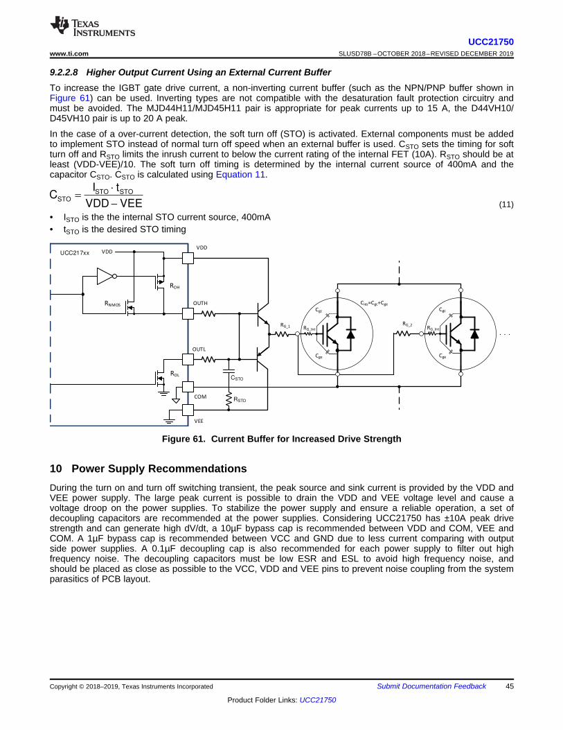
COM
CSTO
VDD
ROH
RNMOS
ROL
OUTH
OUTL
VEE
VDD
RSTO
UCC217xx
Cgc
Cge
Cies=Cgc+Cge
RG_Int
Cgc
Cge
RG_IntRG_1 RG_2
STO STO
STO
I tC
VDD VEE
45
UCC21750www.ti.com SLUSD78B –OCTOBER 2018–REVISED DECEMBER 2019
Product Folder Links: UCC21750
Submit Documentation FeedbackCopyright © 2018–2019, Texas Instruments Incorporated
9.2.2.8 Higher Output Current Using an External Current BufferTo increase the IGBT gate drive current, a non-inverting current buffer (such as the NPN/PNP buffer shown inFigure 61) can be used. Inverting types are not compatible with the desaturation fault protection circuitry andmust be avoided. The MJD44H11/MJD45H11 pair is appropriate for peak currents up to 15 A, the D44VH10/D45VH10 pair is up to 20 A peak.
In the case of a over-current detection, the soft turn off (STO) is activated. External components must be addedto implement STO instead of normal turn off speed when an external buffer is used. CSTO sets the timing for softturn off and RSTO limits the inrush current to below the current rating of the internal FET (10A). RSTO should be atleast (VDD-VEE)/10. The soft turn off timing is determined by the internal current source of 400mA and thecapacitor CSTO. CSTO is calculated using Equation 11.
(11)• ISTO is the the internal STO current source, 400mA• tSTO is the desired STO timing
Figure 61. Current Buffer for Increased Drive Strength
10 Power Supply RecommendationsDuring the turn on and turn off switching transient, the peak source and sink current is provided by the VDD andVEE power supply. The large peak current is possible to drain the VDD and VEE voltage level and cause avoltage droop on the power supplies. To stabilize the power supply and ensure a reliable operation, a set ofdecoupling capacitors are recommended at the power supplies. Considering UCC21750 has ±10A peak drivestrength and can generate high dV/dt, a 10µF bypass cap is recommended between VDD and COM, VEE andCOM. A 1µF bypass cap is recommended between VCC and GND due to less current comparing with outputside power supplies. A 0.1µF decoupling cap is also recommended for each power supply to filter out highfrequency noise. The decoupling capacitors must be low ESR and ESL to avoid high frequency noise, andshould be placed as close as possible to the VCC, VDD and VEE pins to prevent noise coupling from the systemparasitics of PCB layout.

46
UCC21750SLUSD78B –OCTOBER 2018–REVISED DECEMBER 2019 www.ti.com
Product Folder Links: UCC21750
Submit Documentation Feedback Copyright © 2018–2019, Texas Instruments Incorporated
11 Layout
11.1 Layout GuidelinesDue to the strong drive strength of UCC21750, careful considerations must be taken in PCB design. Below aresome key points:• The driver should be placed as close as possible to the power semiconductor to reduce the parasitic
inductance of the gate loop on the PCB traces• The decoupling capacitors of the input and output power supplies should be placed as close as possible to
the power supply pins. The peak current generated at each switching transient can cause high dI/dt andvoltage spike on the parasitic inductance of PCB traces
• The driver COM pin should be connected to the Kelvin connection of SiC MOSFET source or IGBT emitter. Ifthe power device does not have a split Kelvin source or emitter, the COM pin should be connected as closeas possible to the source or emitter terminal of the power device package to separate the gate loop from thehigh power switching loop
• Use a ground plane on the input side to shield the input signals. The input signals can be distorted by thehigh frequency noise generated by the output side switching transients. The ground plane provides a low-inductance filter for the return current flow
• If the gate driver is used for the low side switch which the COM pin connected to the dc bus negative, use theground plane on the output side to shield the output signals from the noise generated by the switch node; ifthe gate driver is used for the high side switch, which the COM pin is connected to the switch node, groundplane is not recommended
• If ground plane is not used on the output side, separate the return path of the DESAT and AIN ground loopfrom the gate loop ground which has large peak source and sink current
• No PCB trace or copper is allowed under the gate driver. A PCB cutout is recommended to avoid any noisecoupling between the input and output side which can contaminate the isolation barrier
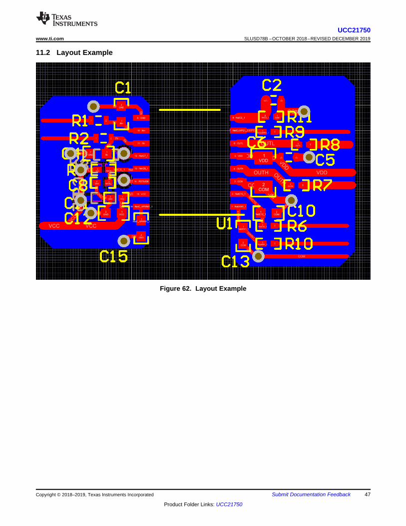
47
UCC21750www.ti.com SLUSD78B –OCTOBER 2018–REVISED DECEMBER 2019
Product Folder Links: UCC21750
Submit Documentation FeedbackCopyright © 2018–2019, Texas Instruments Incorporated
11.2 Layout Example
Figure 62. Layout Example

48
UCC21750SLUSD78B –OCTOBER 2018–REVISED DECEMBER 2019 www.ti.com
Product Folder Links: UCC21750
Submit Documentation Feedback Copyright © 2018–2019, Texas Instruments Incorporated
12 Device and Documentation Support
12.1 Documentation Support
12.1.1 Related DocumentationFor related documentation see the following:• Isolation Glossary
12.2 Receiving Notification of Documentation UpdatesTo receive notification of documentation updates, navigate to the device product folder on ti.com. In the upperright corner, click on Alert me to register and receive a weekly digest of any product information that haschanged. For change details, review the revision history included in any revised document.
12.3 Community ResourceTI E2E™ support forums are an engineer's go-to source for fast, verified answers and design help — straightfrom the experts. Search existing answers or ask your own question to get the quick design help you need.
Linked content is provided "AS IS" by the respective contributors. They do not constitute TI specifications and donot necessarily reflect TI's views; see TI's Terms of Use.
12.4 TrademarksE2E is a trademark of Texas Instruments.
12.5 Electrostatic Discharge CautionThis integrated circuit can be damaged by ESD. Texas Instruments recommends that all integrated circuits be handled withappropriate precautions. Failure to observe proper handling and installation procedures can cause damage.
ESD damage can range from subtle performance degradation to complete device failure. Precision integrated circuits may be moresusceptible to damage because very small parametric changes could cause the device not to meet its published specifications.
12.6 GlossarySLYZ022 — TI Glossary.
This glossary lists and explains terms, acronyms, and definitions.
13 Mechanical, Packaging, and Orderable InformationThe following pages include mechanical packaging and orderable information. This information is the mostcurrent data available for the designated devices. This data is subject to change without notice and revision ofthis document. For browser-based versions of this data sheet, refer to the left-hand navigation.

PACKAGE OPTION ADDENDUM
www.ti.com 10-Dec-2020
Addendum-Page 1
PACKAGING INFORMATION
Orderable Device Status(1)
Package Type PackageDrawing
Pins PackageQty
Eco Plan(2)
Lead finish/Ball material
(6)
MSL Peak Temp(3)
Op Temp (°C) Device Marking(4/5)
Samples
UCC21750DW ACTIVE SOIC DW 16 40 RoHS & Green NIPDAU Level-2-260C-1 YEAR -40 to 125 UCC21750
UCC21750DWR ACTIVE SOIC DW 16 2000 RoHS & Green NIPDAU Level-2-260C-1 YEAR -40 to 125 UCC21750
(1) The marketing status values are defined as follows:ACTIVE: Product device recommended for new designs.LIFEBUY: TI has announced that the device will be discontinued, and a lifetime-buy period is in effect.NRND: Not recommended for new designs. Device is in production to support existing customers, but TI does not recommend using this part in a new design.PREVIEW: Device has been announced but is not in production. Samples may or may not be available.OBSOLETE: TI has discontinued the production of the device.
(2) RoHS: TI defines "RoHS" to mean semiconductor products that are compliant with the current EU RoHS requirements for all 10 RoHS substances, including the requirement that RoHS substancedo not exceed 0.1% by weight in homogeneous materials. Where designed to be soldered at high temperatures, "RoHS" products are suitable for use in specified lead-free processes. TI mayreference these types of products as "Pb-Free".RoHS Exempt: TI defines "RoHS Exempt" to mean products that contain lead but are compliant with EU RoHS pursuant to a specific EU RoHS exemption.Green: TI defines "Green" to mean the content of Chlorine (Cl) and Bromine (Br) based flame retardants meet JS709B low halogen requirements of <=1000ppm threshold. Antimony trioxide basedflame retardants must also meet the <=1000ppm threshold requirement.
(3) MSL, Peak Temp. - The Moisture Sensitivity Level rating according to the JEDEC industry standard classifications, and peak solder temperature.
(4) There may be additional marking, which relates to the logo, the lot trace code information, or the environmental category on the device.
(5) Multiple Device Markings will be inside parentheses. Only one Device Marking contained in parentheses and separated by a "~" will appear on a device. If a line is indented then it is a continuationof the previous line and the two combined represent the entire Device Marking for that device.
(6) Lead finish/Ball material - Orderable Devices may have multiple material finish options. Finish options are separated by a vertical ruled line. Lead finish/Ball material values may wrap to twolines if the finish value exceeds the maximum column width.
Important Information and Disclaimer:The information provided on this page represents TI's knowledge and belief as of the date that it is provided. TI bases its knowledge and belief on informationprovided by third parties, and makes no representation or warranty as to the accuracy of such information. Efforts are underway to better integrate information from third parties. TI has taken andcontinues to take reasonable steps to provide representative and accurate information but may not have conducted destructive testing or chemical analysis on incoming materials and chemicals.TI and TI suppliers consider certain information to be proprietary, and thus CAS numbers and other limited information may not be available for release.
In no event shall TI's liability arising out of such information exceed the total purchase price of the TI part(s) at issue in this document sold by TI to Customer on an annual basis.

PACKAGE OPTION ADDENDUM
www.ti.com 10-Dec-2020
Addendum-Page 2
OTHER QUALIFIED VERSIONS OF UCC21750 :
• Automotive: UCC21750-Q1
NOTE: Qualified Version Definitions:
• Automotive - Q100 devices qualified for high-reliability automotive applications targeting zero defects

www.ti.com
GENERIC PACKAGE VIEW
This image is a representation of the package family, actual package may vary.Refer to the product data sheet for package details.
SOIC - 2.65 mm max heightDW 16SMALL OUTLINE INTEGRATED CIRCUIT7.5 x 10.3, 1.27 mm pitch
4224780/A

www.ti.com
PACKAGE OUTLINE
C
TYP10.639.97
2.65 MAX
14X 1.27
16X 0.510.31
2X8.89
TYP0.330.10
0 - 80.30.1
(1.4)
0.25GAGE PLANE
1.270.40
A
NOTE 3
10.510.1
BNOTE 4
7.67.4
4221009/B 07/2016
SOIC - 2.65 mm max heightDW0016BSOIC
NOTES: 1. All linear dimensions are in millimeters. Dimensions in parenthesis are for reference only. Dimensioning and tolerancing per ASME Y14.5M. 2. This drawing is subject to change without notice. 3. This dimension does not include mold flash, protrusions, or gate burrs. Mold flash, protrusions, or gate burrs shall not exceed 0.15 mm, per side. 4. This dimension does not include interlead flash. Interlead flash shall not exceed 0.25 mm, per side.5. Reference JEDEC registration MS-013.
1 16
0.25 C A B
98
PIN 1 IDAREA
SEATING PLANE
0.1 C
SEE DETAIL A
DETAIL ATYPICAL
SCALE 1.500

www.ti.com
EXAMPLE BOARD LAYOUT
(9.75)R0.05 TYP
0.07 MAXALL AROUND
0.07 MINALL AROUND
(9.3)
14X (1.27)
R0.05 TYP
16X (1.65)
16X (0.6)
14X (1.27)
16X (2)
16X (0.6)
4221009/B 07/2016
SOIC - 2.65 mm max heightDW0016BSOIC
SYMM
SYMM
SEEDETAILS
1
8 9
16
SYMM
HV / ISOLATION OPTION8.1 mm CLEARANCE/CREEPAGE
NOTES: (continued) 6. Publication IPC-7351 may have alternate designs. 7. Solder mask tolerances between and around signal pads can vary based on board fabrication site.
METAL SOLDER MASKOPENING
NON SOLDER MASKDEFINED
SOLDER MASK DETAILS
OPENINGSOLDER MASK METAL
SOLDER MASKDEFINED
LAND PATTERN EXAMPLESCALE:4X
SYMM
1
8 9
16
IPC-7351 NOMINAL7.3 mm CLEARANCE/CREEPAGE
SEEDETAILS
www.ti.com
EXAMPLE STENCIL DESIGN
R0.05 TYPR0.05 TYP
16X (1.65)
16X (0.6)
14X (1.27)
(9.75)
16X (2)
16X (0.6)
14X (1.27)
(9.3)
4221009/B 07/2016
SOIC - 2.65 mm max heightDW0016BSOIC
NOTES: (continued) 8. Laser cutting apertures with trapezoidal walls and rounded corners may offer better paste release. IPC-7525 may have alternate design recommendations. 9. Board assembly site may have different recommendations for stencil design.
SYMM
SYMM
1
8 9
16
HV / ISOLATION OPTION8.1 mm CLEARANCE/CREEPAGE
SOLDER PASTE EXAMPLEBASED ON 0.125 mm THICK STENCIL
SCALE:4X
SYMM
SYMM
1
8 9
16
IPC-7351 NOMINAL7.3 mm CLEARANCE/CREEPAGE
IMPORTANT NOTICE AND DISCLAIMER
TI PROVIDES TECHNICAL AND RELIABILITY DATA (INCLUDING DATASHEETS), DESIGN RESOURCES (INCLUDING REFERENCE DESIGNS), APPLICATION OR OTHER DESIGN ADVICE, WEB TOOLS, SAFETY INFORMATION, AND OTHER RESOURCES “AS IS” AND WITH ALL FAULTS, AND DISCLAIMS ALL WARRANTIES, EXPRESS AND IMPLIED, INCLUDING WITHOUT LIMITATION ANY IMPLIED WARRANTIES OF MERCHANTABILITY, FITNESS FOR A PARTICULAR PURPOSE OR NON-INFRINGEMENT OF THIRD PARTY INTELLECTUAL PROPERTY RIGHTS.These resources are intended for skilled developers designing with TI products. You are solely responsible for (1) selecting the appropriate TI products for your application, (2) designing, validating and testing your application, and (3) ensuring your application meets applicable standards, and any other safety, security, or other requirements. These resources are subject to change without notice. TI grants you permission to use these resources only for development of an application that uses the TI products described in the resource. Other reproduction and display of these resources is prohibited. No license is granted to any other TI intellectual property right or to any third party intellectual property right. TI disclaims responsibility for, and you will fully indemnify TI and its representatives against, any claims, damages, costs, losses, and liabilities arising out of your use of these resources.TI’s products are provided subject to TI’s Terms of Sale (www.ti.com/legal/termsofsale.html) or other applicable terms available either on ti.com or provided in conjunction with such TI products. TI’s provision of these resources does not expand or otherwise alter TI’s applicable warranties or warranty disclaimers for TI products.
Mailing Address: Texas Instruments, Post Office Box 655303, Dallas, Texas 75265Copyright © 2020, Texas Instruments Incorporated