Embed Size (px)
Citation preview

U-Shaped Nano-Apertures for Enhanced Optical Transmission and Resolution
Mustafa Turkmen 1,2,3, Serap Aksu 3,4, A. Engin Çetin2,3, Ahmet A. Yanik 2,3, Alp Artar 2,3, Hatice Altug 2,3,4,*
1Electrical and Electronics Engineering, Erciyes University, Kayseri, 38039, Turkey. 2Electrical and Computer Engineering, 3Photonics Center, 4Materials Science and Engineering,
Boston University, Boston, MA, 02215, USA *E-mail: [email protected]
ABSTRACT
The subject of light transmission through optically thin metal films perforated with arrays of subwavelength nanoholes has recently attracted significant attention. In this work, we present experimental and calculated results on optical transmission/reflection of the U-shaped nanoapertures for enhanced optical transmission and resolution. We propose different structure designs in order to prove the effect of geometry on resonance and enhanced fields. Theoretical calculations of transmission/reflection spectra and field distributions of U-shaped nano-apertures are performed by using 3-dimensional finite-difference time-domain method. The results of these numerical calculations show that transmission through the apertures is indeed concentrated in the gap region. Added to theoretical calculations we also performed a lift-off free plasmonic device fabrication technique based on positive resist electron beam lithography and reactive ion etching in order to fabricate U-shaped nanostructures. After transferring nanopattern on 80 nm thick suspended SiNx membrane using EBL followed by dry etching, a directional metal deposition processes is used to deposit 5 nm thick Ti and 30 nm thick Au layers. Theoretical calculations are supported with experimental results to prove the tunability of resonances with the geometry at the mid-infrared wavelengths which could be used for infrared detection of biomolecules.
KEYWORDS: Nanostructure fabrication, subwavelength structures, nanoplasmonics, optical nanoantenna, optical communications, metamaterials, surface plasmons, near-field effects, infrared spectroscopy.
1. INTRODUCTION
According to classical electrodynamics, transmission intensity of electromagnetic wave through a subwavelength aperture is proportional to the fourth power of the ratio of diameter and wavelength, which turns out to be extremely low [1]. However, it has been experimentally demonstrated by Ebbesen et al. in 1998 that once a metal film is perforated with periodic array of subwavelength apertures, the optical transmission can be tremendously enhanced than that predicted by the diffraction theory [2]. The demonstration of a remarkable transmission through the optically thick metallic film pierced with a periodic array of subwavelength holes has stimulated great interest to probe into the underlying physics mechanism behind the effect and the possible applications [2, 3]. Metamaterials with tunable resonances from mid-IR to visible wavelengths could have far-reaching consequences for chip based optical devices, active filters, optical modulators, and bio-sensors [2-4]. The electromagnetic properties of this kind of metamaterials are derived mainly from the resonating elements rather than atoms or molecules as in conventional materials [4]. A microwave dual-band negative-index metamaterial was fabricated [5] and experimentally confirmed as a multi-frequency resonator [6]. Recently, near-IR metamaterials with dual-band negative-index characteristics were also reported [7]. Obtaining such unique electromagnetic responses require investigation of novel metamaterial designs. As a result, many researchers have focused on subwavelength apertures, resulting in unusual high transmissions in frequency ranges [8-11]. The optical characteristics of the apertures are highly dependent on the refractive index of the adjacent medium [12], the shape of the apertures [13], aperture diameter [14], film thickness [15], and lattice geometry [13, 16].
Photonic Microdevices/Microstructures for Sensing III,edited by Hai Xiao, Xudong Fan, Anbo Wang, Proc. of SPIE Vol. 8034,
80340H · © 2011 SPIE · CCC code: 0277-786X/11/$18 · doi: 10.1117/12.884355
Proc. of SPIE Vol. 8034 80340H-1
Downloaded from SPIE Digital Library on 14 Sep 2011 to 128.197.27.9. Terms of Use: http://spiedl.org/terms

In this study, we propose a U-shaped nano-aperture antenna arrays for enhanced optical transmission and resolution. The schematic view of the proposed structure is shown in Fig. 1. We investigate the spectral response of this metamaterial antenna both numerically and experimentally. In order to understand the physical origin of the multi-resonant behavior, we analyze the structure by 3-dimensional finite difference time domain (FDTD) method and obtain the field distributions. We also determine the parameters that can enable fine control of the resonance features. Due to the multi-spectral response and enhanced near field distributions, the proposed antennas can be useful for wide range of applications, such as wavelength-tunable active filters, optical modulators, ultrafast switching devices, and biosensing.
Figure 1. The schematic view of the proposed U-shaped nano-aperture antenna arrays (a) Top view including the geometrical parameters: L, the length, H, the height, w, and the gap width of the aperture. The y-polarized illumination source is indicated in the figure as well. (b) Side view representing the layers of the proposed antenna geometry: 30 nm thick Au, 5 nm thick Ti, and 80 nm thick SiNx layers.
2. SIMULATION AND FABRICATION Fig. 1 shows the schematic view of the proposed U-shaped metamaterial antenna design. In this figure, L indicates the length of the structure, H indicates the height, and w indicates the gap width. We investigate the spectral response of the proposed antenna both numerically and experimentally. For the numerical analysis, the U-shaped nano-aperture antennas are modeled by FDTD method [17]. During the simulations, the frequency dependent dielectric parameters of the metals are taken from [18]. In the unit cell, consist of the two individual elements, periodic boundary conditions is used along x and y axes and perfectly matched layers are used along +z, the direction of the illumination source.
The scanning electron microscope (SEM) image and the optical responses of the fabricated nanostructures are shown in Fig. 2. Calculated and measured reflection spectra, given in Fig. 2(a) and 2(b), clearly show that the proposed U-shaped nano-aperture antenna have dual-band resonances at the mid-IR wavelengths. For the experimental demonstration of the calculated multi-resonant characteristic, the proposed U-shaped nano-aperture antennas are fabricated on a free standing 80 nm thick silicon nitride (SiNx) membrane. Fabricated structures are characterized optically by a Fourier transform infrared (FTIR) microscope. Our experimental set-up consists of an IR microscope coupled to a BrukerTM FTIR spectrometer with a KBr splitter. Electromagnetic radiation, normally incident to the array (along the z-direction shown in Fig. 1) with the incident E-field polarized parallel to the aperture arms, is used to efficiently couple the light to the resonators. Polarized light source is normally incident on the nanopatterned surface. Reflected infrared signal is collected by a Cassagrian reflection optics (NA = 0.4) and coupled into a liquid N2-cooled mercury cadmium telluride detector. Reflection data are normalized using an optically thin gold standard.
Proc. of SPIE Vol. 8034 80340H-2
Downloaded from SPIE Digital Library on 14 Sep 2011 to 128.197.27.9. Terms of Use: http://spiedl.org/terms
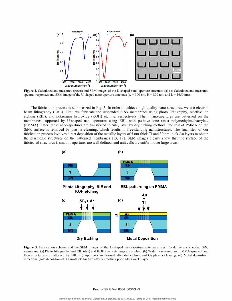
Figure 2. Calculated and measured spectra and SEM images of the U-shaped nano-aperture antennas. (a)-(c) Calculated and measured spectral responses and SEM image of the U-shaped nano-aperture antennas (w = 190 nm, H = 800 nm, and L = 1650 nm).
The fabrication process is summarized in Fig. 3. In order to achieve high quality nano-structures, we use electron beam lithography (EBL). First, we fabricate the suspended SiNx membranes using photo lithography, reactive ion etching (RIE), and potassium hydroxide (KOH) etching, respectively. Then, nano-apertures are patterned on the membranes supported by U-shaped nano-apertures using EBL with positive tone resist polymethylmethacrylate (PMMA). Later, these nano-apertures are transferred to SiNx layer by dry etching method. The rest of PMMA on the SiNx surface is removed by plasma cleaning, which results in free-standing nanostructures. The final step of our fabrication process involves direct deposition of the metallic layers of 5 nm-thick Ti and 30 nm-thick Au layers to obtain the plasmonic structures on the patterned membranes [13, 19]. SEM images clearly show that the surface of the fabricated structures is smooth, apertures are well defined, and unit cells are uniform over large areas.
Figure 3. Fabrication scheme and the SEM images of the U-shaped nano-aperture antenna arrays. To define a suspended SiNx membrane, (a) Photo lithography and RIE (dry) and KOH (wet) etchings are applied. (b) Wafer is reversed and PMMA spinned, and then structures are patterned by EBL. (c) Apertures are formed after dry etching and O2 plasma cleaning. (d) Metal deposition; directional gold deposition of 30 nm-thick Au film after 5 nm-thick prior adhesion Ti layer.
Proc. of SPIE Vol. 8034 80340H-3
Downloaded from SPIE Digital Library on 14 Sep 2011 to 128.197.27.9. Terms of Use: http://spiedl.org/terms

3. RESULTS In order to understand the physical origin of the dual-band response of the U-shaped nano-apertures, we perform numerical simulations using FDTD method. We show the field distributions corresponding to two distinct resonance dips (λ1 and λ2). The z-component of the magnetic field intensities inside the metal layer, |Hz|2, at the reflectance dips are shown in Fig. 4(a) and 4(b). These figures show that the first mode is mainly located at the top of the arms and second one is located at both top and corners of the U-shaped aperture. The lower order mode has two strong lobes, which are located at the arm ends of the apertures. Similarly, the second mode which is the higher mode of the U-shaped aperture has four lobes, two of them are located at the arm ends and the rest is located at the corners of the vertical aperture. Hence, these modes are the fundamental modes of the U-shaped nano-aperture antennas.
To determine the near field enhancement, we also show the total electric field intensities, |E|2, of the two modes of the U-shaped nano-aperture antennas in Fig. 4(c) and 4(d). The near field enhancements are larger than 2000 times for the first mode as shown in Fig. 4(c), which are highly desirable for Raman, fluorescence, and infrared spectroscopy. Furthermore, these field enhancements are mainly located within the apertures. This is highly desirable for biosensing applications as it increases the overlap of the analytes with the electromagnetic field inside the aperture.
Figure 4. Field distributions (|Hz|2 and |E|2) of the U-shaped nano-aperture antennas inside the metallic layer (z = 15 nm) at the reflection dips with the corresponding parameters; L = 1200 nm, w = 100 nm and H = 800 nm.
As shown in Fig. 4, the fields in each resonance dip primarily concentrates at the arm ends and the corners of the aperture. Hence, we obtain the spectral response of the structure both experimentally and numerically. To find a control mechanism of the spectral response of the metamaterial antennas, we determine the dependence of the spectra on geometrical parameters including L, H, and w. We fabricated different U-shaped nano-aperture antennas for the experimental investigation of the parameter dependence. The results of these experiments are illustrated in Fig. 5(a), 5(b), and 5(c), for w, H, and L, respectively. Increasing length (L) slightly changes the resonance locations while increasing gap width (w) and height (H) result in a strong red-shift in the reflection spectrum. Although our proposed structure operate in mid-IR frequency range, by scaling the geometry the resonance locations can be tuned over a wide range, from mid-IR to visible wavelengths.
Proc. of SPIE Vol. 8034 80340H-4
Downloaded from SPIE Digital Library on 14 Sep 2011 to 128.197.27.9. Terms of Use: http://spiedl.org/terms

Figure 5. Calculated reflection spectra of the U-shaped nanoaperture antennas for different cases (a) L and H are fixed while w is varied (L = 1200 nm and H = 600 nm) (b) w and L are fixed while H is varied (L = 1200 nm and w = 100 nm) and (c) w, and H are fixed while L is varied (H = 800 nm and w = 100 nm).
4. CONCLUSION
In conclusion, we introduce a dual-band metamaterial design based on U-shaped nano-apertures. By using this nanostructured resonator, we show that light can be manipulated on a chip and dual-band resonant behavior can be obtained. We have also investigated the dependence of the resonance behavior on each individual geometrical parameter such as gap width, length, and height. We have shown that the resonance shows a linear dependence on the aperture width, length and height of the U-shaped structure. This behavior gives the advantage to tune the operating frequency by varying the geometrical parameters. The highly enhanced near field properties depend on the perimeter of the apertures can be useful for the near field imaging. The proposed nano-aperture antenna can also support dual-band of operations and act as a highly frequency selective device. Metamaterials with tunable resonances from mid-IR to visible wavelengths could have far-reaching consequences for chip based optical devices, active filters, optical modulators, and bio-sensors. Finally, our design shows high near-field resolution, which can be useful for near field imaging and surface enhanced spectroscopy. Future work may include studying systems and bio-responses of nano-aperture based metamaterials, in which both transverse and longitudinal inductive coupling are involved. This idea offers additional degrees of flexibility for designing structures and optimizing the physical response of metamaterials at optical frequencies.
5. REFERENCES
[1] Bethe, H. A., “Theory of diffraction by small holes”, Phys. Rev., 66, p. 163 (1944).
[2] Ebbesen, T. W., Lezec, H. J., Ghaemi, H., Thio, T., Wolf, P. A., “Extraordinary optical transmission through sub-wavelength hole arrays,” Nature, 391, pp. 667-669 (1998).
Proc. of SPIE Vol. 8034 80340H-5
Downloaded from SPIE Digital Library on 14 Sep 2011 to 128.197.27.9. Terms of Use: http://spiedl.org/terms

[3] Genet, C., Ebbesen, T.W., “Light in tiny holes”, Nature, 445, pp. 39-46 (2007).
[4] Pendry, J. B., “Metamaterials in the sunshine,” Nature Materials, 5, pp. 599-600 (2006).
[5] Chen, H. Ran, L., Huangfu, J., Zhang, X., Chen, K., Grzegorczyk, T. M., Kong, J. A., “Metamaterial exhibiting left-handed properties over multiple frequency bands,” Journal of Applied Physics, 96, pp. 5338-5340 (2004).
[6] Wang, D., Ran, L., Wu, B. I., Chen, H., Huangfu, J., Grzegorczyk, T. M., Kong, J. A., “Multi-frequency resonator based on dual-band S-shaped left-handed material,” Optics Express, 14, p. 12288 (2006).
[7] Kwon, D.-H., Werner, D. H., Kildishev, A. V., Shalaev, V. M., “Near-infrared metamaterials with dual-band negative-index characteristics,” Optics Express, 15, p. 1647 (2007).
[8] Degiron, A., Lezec, H. J., Yamamoto, N., Ebbesen, T. W., “Optical transmission properties of a single subwavelength aperture in a real metal,” Opt. Commun., 239, pp. 61-66 (2004).
[9] Degiron, A., Ebbesen, T. W., “The role of localized surface plasmon modes in the enhanced transmission of periodic subwavelength apertures,” J. Opt. A: Pure Appl. Opt., 7, pp. 90-96 (2005).
[10] Matsui, T., Agrawal, A., Nahata, A., Vardeny, Z. V., “Transmission resonances through a periodic arrays of subwavelength aperture,” Nature, 446, pp. 517-521 (2007).
[11] Hou, B., Hang, Z. H., Wen, W., Chan, C. T., Sheng, P., “Microwave transmission through metallic hole arrays: Surface electric field measurements,” Appl. Phys. Lett., 89, p. 131917 (2006).
[12] Kim, T. J., Thio, T., Ebbesen, T. W., Grupp, D. E., Lezec, H. J., “Control of optical transmission through metals perforated with subwavelength hole arrays,” Optics Letters, 24, p. 256 (1999).
[13] Yanik, A. A., Wang, X., Erramilli, S., Hong, M. K., Altug, H., “Extraordinary midinfrared transmission of rectangular coaxial nanoaperture arrays,” Appl. Phys. Lett., 93, p. 081104 (2008).
[14] Azad, A. K., Zhao, Y., Zhang, W., “Transmission properties of terahertz pulses through an ultrathin subwavelength silicon hole array,” Appl. Phys. Lett., 86, p. 141102 (2005).
[15] Degiron, A., Lezec, H. J., Barnes, W. L., Ebbesen, T. W., “Effects of hole depth on enhanced light transmission through subwavelength hole arrays,” Appl. Phys. Lett., 81, p. 4327 (2002).
[16] Ebbesen, T. W., Lezec, H. J., Ghaemi, H., Thio, T., Wolf, P. A., “Extraordinary optical transmission through sub-wavelength hole arrays,” Nature, 391, pp. 667-669 (1998).
[17] The numerical simulations are carried out using a finite-difference-time-domain package, Lumerical FDTD Solutions.
[18] Palik, E. D., “Handbook of Optical Constants of Solids”, Academic, Orlando, FL, 1985.
[19] Yanik, A. A., Huang, M., Artar, A., Chang, T-Y., Altug, H., "Integrated Nanoplasmonic-Nanofluidic Biosensors with Targeted Delivery of Analytes”, Applied Physics Letters, 96, p. 021101 (2010).
Proc. of SPIE Vol. 8034 80340H-6
Downloaded from SPIE Digital Library on 14 Sep 2011 to 128.197.27.9. Terms of Use: http://spiedl.org/terms


![arXiv:1404.0440v1 [physics.optics] 2 Apr 2014 · sample using a high numerical aperture (NA= 1:1) microscope objective. The samples are circular nano-apertures drilled in a 200 nm](https://img.dokumen.tips/doc/110x75/5e8012299f396862505a7c52/arxiv14040440v1-2-apr-2014-sample-using-a-high-numerical-aperture-na-11.jpg)