Embed Size (px)
Citation preview
www.ti.com
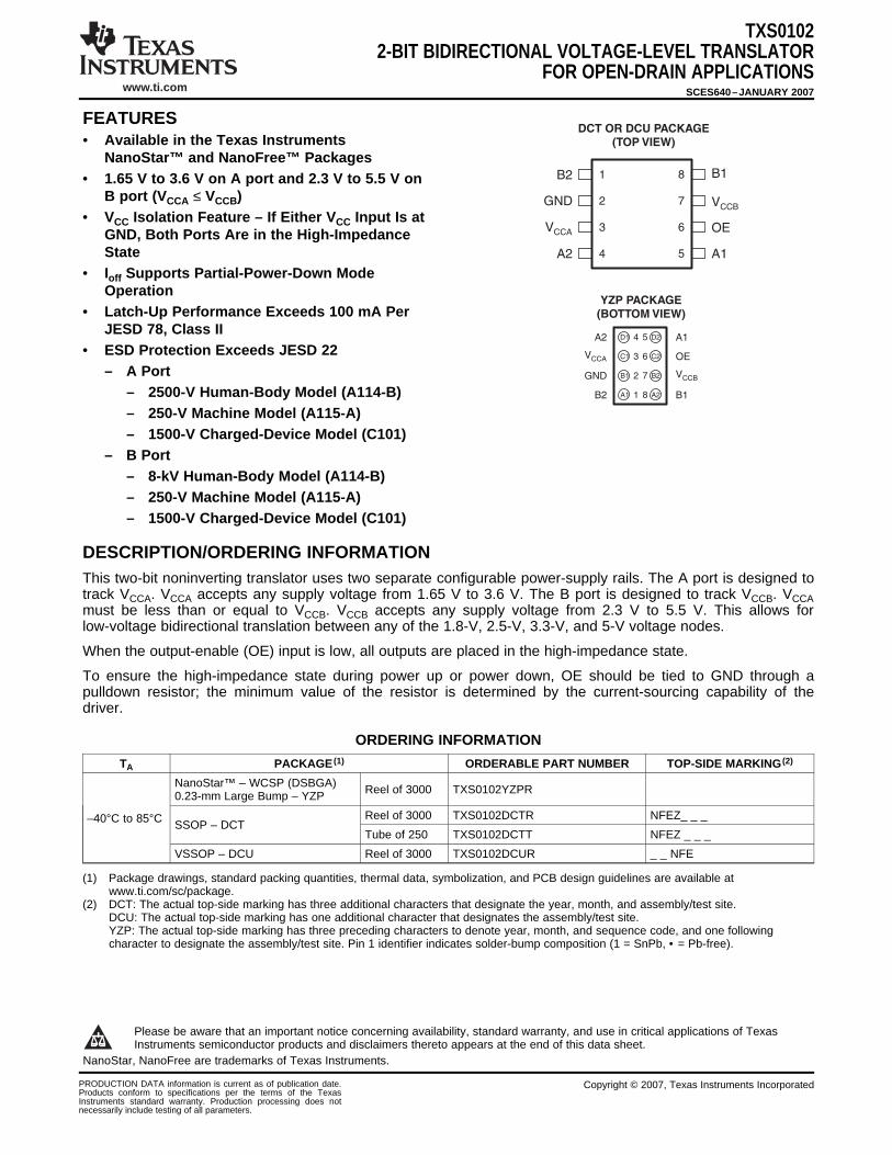
FEATURESDCT OR DCU PACKAGE
(TOP VIEW)
1 B18
2 7 VCCB
3 6 OE
4 5
B2
GND
VCCA
A2 A1
YZP PACKAGE
(BOTTOM VIEW)
A2 54 A1
3 6 OEVCCA
2 7 VCCBGND
8 B11B2 A1
B1
C1
D1
A2
B2
C2
D2
abc
DESCRIPTION/ORDERING INFORMATION
TXS01022-BIT BIDIRECTIONAL VOLTAGE-LEVEL TRANSLATOR
FOR OPEN-DRAIN APPLICATIONSSCES640–JANUARY 2007
• Available in the Texas InstrumentsNanoStar™ and NanoFree™ Packages
• 1.65 V to 3.6 V on A port and 2.3 V to 5.5 V onB port (VCCA ≤ VCCB)
• VCC Isolation Feature – If Either VCC Input Is atGND, Both Ports Are in the High-ImpedanceState
• Ioff Supports Partial-Power-Down ModeOperation
• Latch-Up Performance Exceeds 100 mA PerJESD 78, Class II
• ESD Protection Exceeds JESD 22– A Port
– 2500-V Human-Body Model (A114-B)– 250-V Machine Model (A115-A)– 1500-V Charged-Device Model (C101)
– B Portabc
– 8-kV Human-Body Model (A114-B)abc
– 250-V Machine Model (A115-A)abc– 1500-V Charged-Device Model (C101)
This two-bit noninverting translator uses two separate configurable power-supply rails. The A port is designed totrack VCCA. VCCA accepts any supply voltage from 1.65 V to 3.6 V. The B port is designed to track VCCB. VCCAmust be less than or equal to VCCB. VCCB accepts any supply voltage from 2.3 V to 5.5 V. This allows forlow-voltage bidirectional translation between any of the 1.8-V, 2.5-V, 3.3-V, and 5-V voltage nodes.
When the output-enable (OE) input is low, all outputs are placed in the high-impedance state.
To ensure the high-impedance state during power up or power down, OE should be tied to GND through apulldown resistor; the minimum value of the resistor is determined by the current-sourcing capability of thedriver.
ORDERING INFORMATION
TA PACKAGE (1) ORDERABLE PART NUMBER TOP-SIDE MARKING (2)
NanoStar™ – WCSP (DSBGA) Reel of 3000 TXS0102YZPR0.23-mm Large Bump – YZP
Reel of 3000 TXS0102DCTR NFEZ_ _ _–40°C to 85°C SSOP – DCTTube of 250 TXS0102DCTT NFEZ _ _ _
VSSOP – DCU Reel of 3000 TXS0102DCUR _ _ NFE
(1) Package drawings, standard packing quantities, thermal data, symbolization, and PCB design guidelines are available atwww.ti.com/sc/package.
(2) DCT: The actual top-side marking has three additional characters that designate the year, month, and assembly/test site.DCU: The actual top-side marking has one additional character that designates the assembly/test site.YZP: The actual top-side marking has three preceding characters to denote year, month, and sequence code, and one followingcharacter to designate the assembly/test site. Pin 1 identifier indicates solder-bump composition (1 = SnPb, • = Pb-free).
Please be aware that an important notice concerning availability, standard warranty, and use in critical applications of TexasInstruments semiconductor products and disclaimers thereto appears at the end of this data sheet.
NanoStar, NanoFree are trademarks of Texas Instruments.
PRODUCTION DATA information is current as of publication date. Copyright © 2007, Texas Instruments IncorporatedProducts conform to specifications per the terms of the TexasInstruments standard warranty. Production processing does notnecessarily include testing of all parameters.
www.ti.com
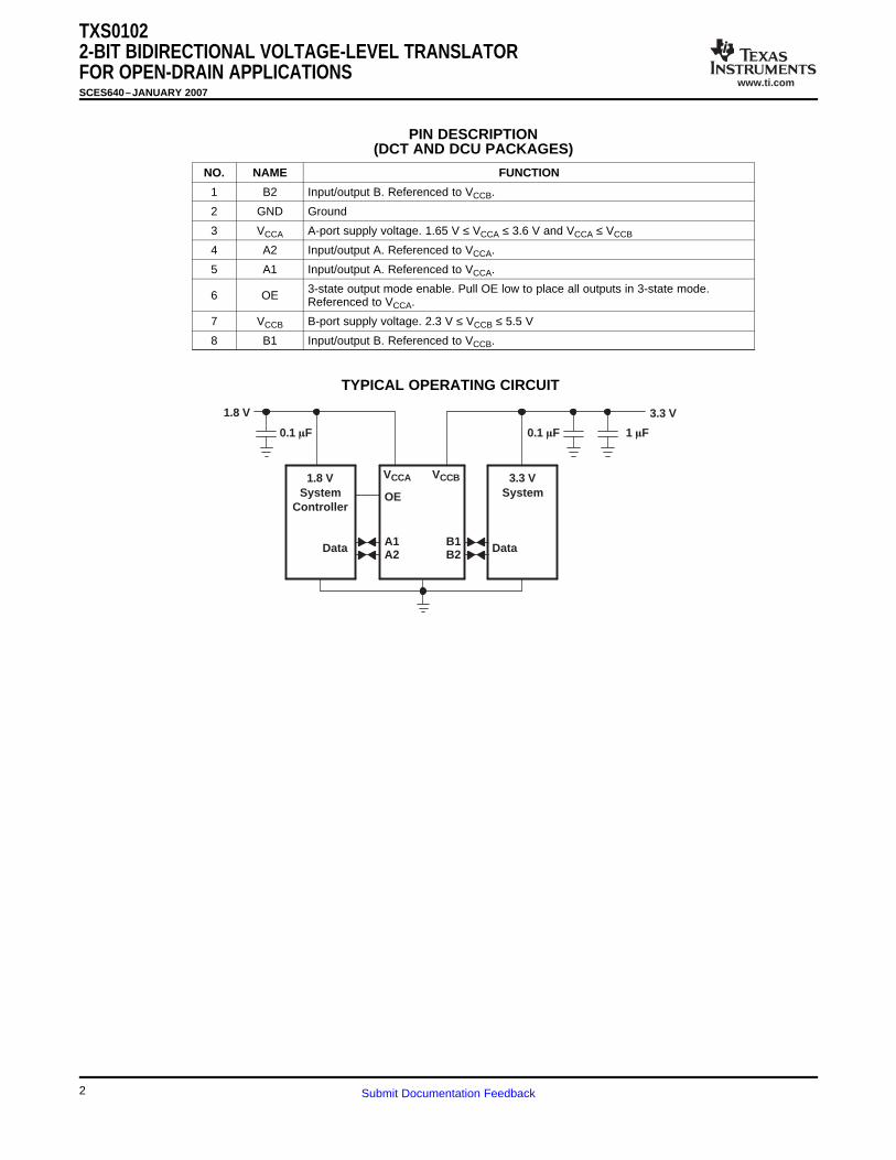
DataData A1 B1
VCCA VCCB
OE
1.8 VSystem
Controller
3.3 VSystem
3.3 V1.8 V
A2 B2
0.1 F0.1 F 1 F
TXS01022-BIT BIDIRECTIONAL VOLTAGE-LEVEL TRANSLATORFOR OPEN-DRAIN APPLICATIONSSCES640–JANUARY 2007
PIN DESCRIPTION(DCT AND DCU PACKAGES)
NO. NAME FUNCTION
1 B2 Input/output B. Referenced to VCCB.
2 GND Ground
3 VCCA A-port supply voltage. 1.65 V ≤ VCCA ≤ 3.6 V and VCCA ≤ VCCB
4 A2 Input/output A. Referenced to VCCA.
5 A1 Input/output A. Referenced to VCCA.
3-state output mode enable. Pull OE low to place all outputs in 3-state mode.6 OE Referenced to VCCA.
7 VCCB B-port supply voltage. 2.3 V ≤ VCCB ≤ 5.5 V
8 B1 Input/output B. Referenced to VCCB.
TYPICAL OPERATING CIRCUIT
2 Submit Documentation Feedback
www.ti.com
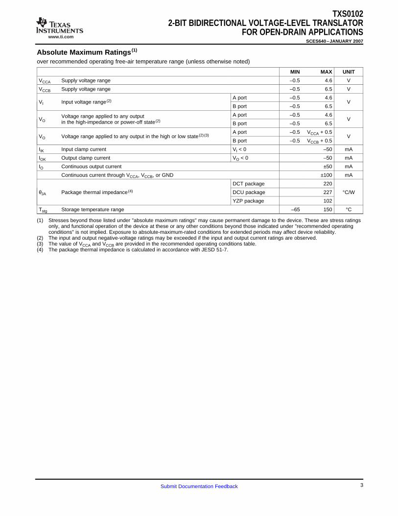
Absolute Maximum Ratings (1)
TXS01022-BIT BIDIRECTIONAL VOLTAGE-LEVEL TRANSLATOR
FOR OPEN-DRAIN APPLICATIONSSCES640–JANUARY 2007
over recommended operating free-air temperature range (unless otherwise noted)
MIN MAX UNIT
VCCA Supply voltage range –0.5 4.6 V
VCCB Supply voltage range –0.5 6.5 V
A port –0.5 4.6VI Input voltage range (2) V
B port –0.5 6.5
A port –0.5 4.6Voltage range applied to any outputVO Vin the high-impedance or power-off state (2) B port –0.5 6.5
A port –0.5 VCCA + 0.5VO Voltage range applied to any output in the high or low state (2) (3) V
B port –0.5 VCCB + 0.5
IIK Input clamp current VI < 0 –50 mA
IOK Output clamp current VO < 0 –50 mA
IO Continuous output current ±50 mA
Continuous current through VCCA, VCCB, or GND ±100 mA
DCT package 220
θJA Package thermal impedance (4) DCU package 227 °C/W
YZP package 102
Tstg Storage temperature range –65 150 °C
(1) Stresses beyond those listed under "absolute maximum ratings" may cause permanent damage to the device. These are stress ratingsonly, and functional operation of the device at these or any other conditions beyond those indicated under "recommended operatingconditions" is not implied. Exposure to absolute-maximum-rated conditions for extended periods may affect device reliability.
(2) The input and output negative-voltage ratings may be exceeded if the input and output current ratings are observed.(3) The value of VCCA and VCCB are provided in the recommended operating conditions table.(4) The package thermal impedance is calculated in accordance with JESD 51-7.
3Submit Documentation Feedback
www.ti.com
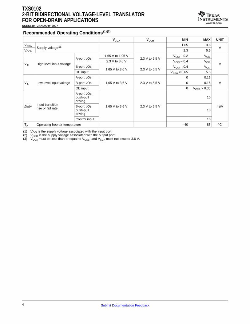
Recommended Operating Conditions (1) (2)
TXS01022-BIT BIDIRECTIONAL VOLTAGE-LEVEL TRANSLATORFOR OPEN-DRAIN APPLICATIONSSCES640–JANUARY 2007
VCCA VCCB MIN MAX UNIT
VCCA 1.65 3.6Supply voltage (3) V
VCCB 2.3 5.5
1.65 V to 1.95 V VCCI – 0.2 VCCIA-port I/Os 2.3 V to 5.5 V
2.3 V to 3.6 V VCCI – 0.4 VCCIVIH High-level input voltage V
B-port I/Os VCCI – 0.4 VCCI1.65 V to 3.6 V 2.3 V to 5.5 V
OE input VCCA × 0.65 5.5
A-port I/Os 0 0.15
VIL Low-level input voltage B-port I/Os 1.65 V to 3.6 V 2.3 V to 5.5 V 0 0.15 V
OE input 0 VCCA × 0.35
A-port I/Os,push-pull 10driving
Input transition∆t/∆v B-port I/Os, 1.65 V to 3.6 V 2.3 V to 5.5 V ns/Vrise or fall rate push-pull 10driving
Control input 10
TA Operating free-air temperature –40 85 °C
(1) VCCI is the supply voltage associated with the input port.(2) VCCO is the supply voltage associated with the output port.(3) VCCA must be less than or equal to VCCB, and VCCA must not exceed 3.6 V.
4 Submit Documentation Feedback
www.ti.com
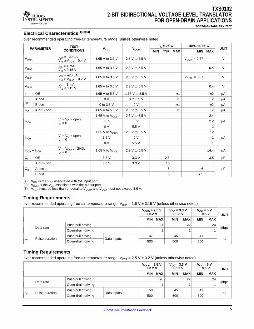
Electrical Characteristics (1) (2) (3)
Timing Requirements
Timing Requirements
TXS01022-BIT BIDIRECTIONAL VOLTAGE-LEVEL TRANSLATOR
FOR OPEN-DRAIN APPLICATIONSSCES640–JANUARY 2007
over recommended operating free-air temperature range (unless otherwise noted)
TA = 25°C –40°C to 85°CTESTPARAMETER VCCA VCCB UNITCONDITIONS MIN TYP MAX MIN MAX
IOH = –20 µA,VOHA 1.65 V to 3.6 V 2.3 V to 5.5 V VCCA × 0.67 VVIB ≥ VCCB – 0.4 V
IOL = 1 mA,VOLA 1.65 V to 3.6 V 2.3 V to 5.5 V 0.4 VVIB ≤ 0.15 V
IOH = –20 µA,VOHB 1.65 V to 3.6 V 2.3 V to 5.5 V VCCB × 0.67 VVIA ≥ VCCA – 0.2 V
IOL = 1 mA,VOLB 1.65 V to 3.6 V 2.3 V to 5.5 V 0.4 VVIA ≤ 0.15 V
II OE 1.65 V to 5.5 V 1.65 V to 5.5 V ±1 ±2 µA
A port 0 V 0 to 5.5 V ±1 ±2 µAIoff
B port 0 to 3.6 V 0 V ±1 ±2 µA
IOZ A or B port 1.65 V to 5.5 V 2.3 V to 5.5 V ±1 ±2 µA
1.65 V to VCCB 2.3 V to 5.5 V 2.4VI = VO = open,ICCA 3.6 V 0 V 2.2 µAIO = 0
0 V 5.5 V –1
1.65 V to VCCB 2.3 V to 5.5 V 12VI = VO = open,ICCB 3.6 V 0 V –1 µAIO = 0
0 V 5.5 V 1
VI = VCCI or GND,ICCA + ICCB 1.65 V to VCCB 2.3 V to 5.5 V 14.4 µAIO = 0
CI OE 3.3 V 3.3 V 2.5 3.5 pF
A or B port 3.3 V 3.3 V 10
Cio A port 5 6 pF
B port 6 7.5
(1) VCCI is the VCC associated with the input port.(2) VCCO is the VCC associated with the output port.(3) VCCA must be less than or equal to VCCB, and VCCA must not exceed 3.6 V.
over recommended operating free-air temperature range, VCCA = 1.8 V ± 0.15 V (unless otherwise noted)
VCCB = 2.5 V VCC = 3.3 V VCC = 5 V± 0.2 V ± 0.3 V ± 0.5 V UNITMIN MAX MIN MAX MIN MAX
Push-pull driving 21 22 24Data rate Mbps
Open-drain driving 1 1 1
Push-pull driving 47 45 41tw Pulse duration Data inputs ns
Open-drain driving 500 500 500
over recommended operating free-air temperature range, VCCA = 2.5 V ± 0.2 V (unless otherwise noted)
VCCB = 2.5 V VCC = 3.3 V VCC = 5 V± 0.2 V ± 0.3 V ± 0.5 V UNITMIN MAX MIN MAX MIN MAX
Push-pull driving 20 22 24Data rate Mbps
Open-drain driving 1 1 1
Push-pull driving 50 45 41tw Pulse duration Data inputs ns
Open-drain driving 500 500 500
5Submit Documentation Feedback
www.ti.com
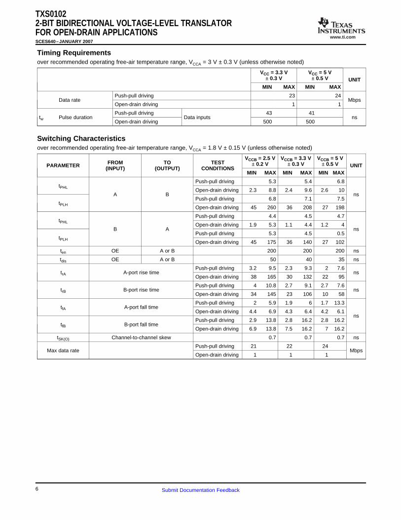
Timing Requirements
Switching Characteristics
TXS01022-BIT BIDIRECTIONAL VOLTAGE-LEVEL TRANSLATORFOR OPEN-DRAIN APPLICATIONSSCES640–JANUARY 2007
over recommended operating free-air temperature range, VCCA = 3 V ± 0.3 V (unless otherwise noted)
VCC = 3.3 V VCC = 5 V± 0.3 V ± 0.5 V UNIT
MIN MAX MIN MAX
Push-pull driving 23 24Data rate Mbps
Open-drain driving 1 1
Push-pull driving 43 41tw Pulse duration Data inputs ns
Open-drain driving 500 500
over recommended operating free-air temperature range, VCCA = 1.8 V ± 0.15 V (unless otherwise noted)
VCCB = 2.5 V VCCB = 3.3 V VCCB = 5 VFROM TO TEST ± 0.2 V ± 0.3 V ± 0.5 VPARAMETER UNIT(INPUT) (OUTPUT) CONDITIONS
MIN MAX MIN MAX MIN MAX
Push-pull driving 5.3 5.4 6.8tPHL
Open-drain driving 2.3 8.8 2.4 9.6 2.6 10A B ns
Push-pull driving 6.8 7.1 7.5tPLH
Open-drain driving 45 260 36 208 27 198
Push-pull driving 4.4 4.5 4.7tPHL
Open-drain driving 1.9 5.3 1.1 4.4 1.2 4B A ns
Push-pull driving 5.3 4.5 0.5tPLH
Open-drain driving 45 175 36 140 27 102
ten OE A or B 200 200 200 ns
tdis OE A or B 50 40 35 ns
Push-pull driving 3.2 9.5 2.3 9.3 2 7.6trA A-port rise time ns
Open-drain driving 38 165 30 132 22 95
Push-pull driving 4 10.8 2.7 9.1 2.7 7.6trB B-port rise time ns
Open-drain driving 34 145 23 106 10 58
Push-pull driving 2 5.9 1.9 6 1.7 13.3tfA A-port fall time
Open-drain driving 4.4 6.9 4.3 6.4 4.2 6.1ns
Push-pull driving 2.9 13.8 2.8 16.2 2.8 16.2tfB B-port fall time
Open-drain driving 6.9 13.8 7.5 16.2 7 16.2
tSK(O) Channel-to-channel skew 0.7 0.7 0.7 ns
Push-pull driving 21 22 24Max data rate Mbps
Open-drain driving 1 1 1
6 Submit Documentation Feedback

www.ti.com
Switching Characteristics
TXS01022-BIT BIDIRECTIONAL VOLTAGE-LEVEL TRANSLATOR
FOR OPEN-DRAIN APPLICATIONSSCES640–JANUARY 2007
over recommended operating free-air temperature range, VCCA = 2.5 V ± 0.2 V (unless otherwise noted)
VCCB = 2.5 V VCCB = 3.3 V VCCB = 5 VFROM TO TEST ± 0.2 V ± 0.3 V ± 0.5 VPARAMETER UNIT(INPUT) (OUTPUT) CONDITIONS
MIN MAX MIN MAX MIN MAX
Push-pull driving 3.2 3.7 3.8tPHL
Open-drain driving 1.7 6.3 2 6 2.1 5.8A B ns
Push-pull driving 3.5 4.1 4.4tPLH
Open-drain driving 43 250 36 206 27 190
Push-pull driving 3 3.6 4.3tPHL
Open-drain driving 1.8 4.7 2.6 4.2 1.2 4B A ns
Push-pull driving 2.5 1.6 1tPLH
Open-drain driving 44 170 37 140 27 103
ten OE A or B 200 200 200 ns
tdis OE A or B 50 40 35 ns
Push-pull driving 2.8 7.4 2.6 6.6 1.8 5.6trA A-port rise time ns
Open-drain driving 34 149 28 121 24 89
Push-pull driving 3.2 8.3 2.9 7.2 2.4 6.1trB B-port rise time ns
Open-drain driving 35 151 24 112 12 64
Push-pull driving 1.9 5.7 1.9 5.5 1.8 5.3tfA A-port fall time ns
Open-drain driving 4.4 6.9 4.3 6.2 4.2 5.8
Push-pull driving 2.2 7.8 2.4 6.7 2.6 6.6tfB B-port fall time ns
Open-drain driving 5.1 8.8 5.4 9.4 5.4 10.4
tSK(O) Channel-to-channel skew 0.7 0.7 0.7 ns
Push-pull driving 20 22 24Max data rate Mbps
Open-drain driving 1 1 1
7Submit Documentation Feedback
www.ti.com
Switching Characteristics
PRINCIPLES OF OPERATION
Applications
Architecture
TXS01022-BIT BIDIRECTIONAL VOLTAGE-LEVEL TRANSLATORFOR OPEN-DRAIN APPLICATIONSSCES640–JANUARY 2007
over recommended operating free-air temperature range, VCCA = 3.3 V ± 0.3 V (unless otherwise noted)
VCCB = 3.3 V VCCB = 5 VFROM TO TEST ± 0.3 V ± 0.5 VPARAMETER UNIT(INPUT) (OUTPUT) CONDITIONS
MIN MAX MIN MAX
Push-pull driving 2.4 3.1tPHL
Open-drain driving 1.3 4.2 1.4 4.6A B ns
Push-pull driving 4.2 4.4tPLH
Open-drain driving 36 204 28 165
Push-pull driving 2.5 3.3tPHL
Open-drain driving 1 124 1 97B A ns
Push-pull driving 2.5 2.6tPLH
Open-drain driving 3 139 3 105
ten OE A or B 200 200 ns
tdis OE A or B 40 35 ns
Push-pull driving 2.3 5.6 1.9 4.8trA A-port rise time ns
Open-drain driving 25 116 19 85
Push-pull driving 2.5 6.4 2.1 7.4trB B-port rise time ns
Open-drain driving 26 116 14 72
Push-pull driving 2 5.4 1.9 5tfA A-port fall time ns
Open-drain driving 4.3 6.1 4.2 5.7
Push-pull driving 2.3 7.4 2.4 7.6tfB B-port fall time ns
Open-drain driving 5 7.6 4.8 8.3
tSK(O) Channel-to-channel skew 0.7 0.7 ns
Push-pull driving 23 24Max data rate Mbps
Open-drain driving 1 1
The TXS0102 can be used in level-translation applications for interfacing devices or systems operating atdifferent interface voltages with one another. The TXS0102 is ideal for use in applications where an open-draindriver is connected to the data I/Os. The TXS0102 can also be used in applications where a push-pull driver isconnected to the data I/Os, but the TXB0102 might be a better option for such push-pull applications.
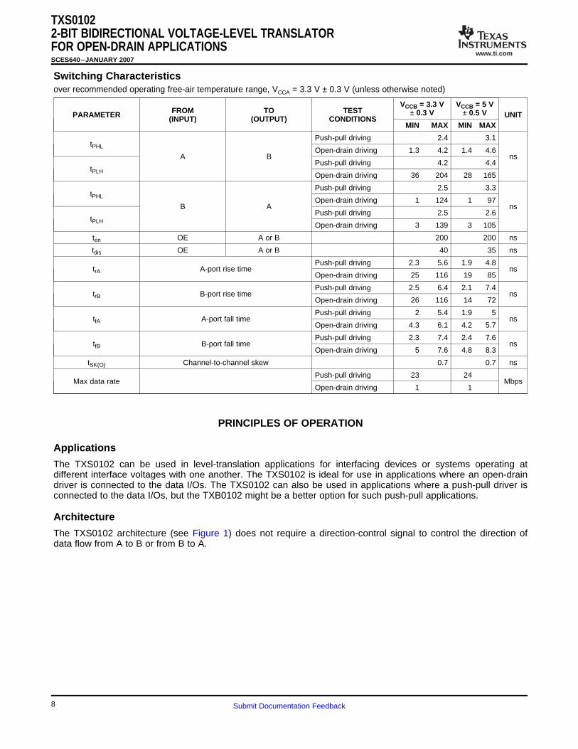
The TXS0102 architecture (see Figure 1) does not require a direction-control signal to control the direction ofdata flow from A to B or from B to A.
8 Submit Documentation Feedback
www.ti.com
VCCB
B
VCCA VCCB
Gate Bias
One-
shot
One-
shot
10k 10k
T1 T2
A
Input Driver Requirements
Power Up
Enable and Disable
Pullup or Pulldown Resistors on I/O Lines
TXS01022-BIT BIDIRECTIONAL VOLTAGE-LEVEL TRANSLATOR
FOR OPEN-DRAIN APPLICATIONSSCES640–JANUARY 2007
PRINCIPLES OF OPERATION (continued)
Figure 1. Architecture of a TXS01xx Cell
Each A-port I/O has an internal 10-kΩ pullup resistor to VCCA, and each B-port I/O has an internal 10-kΩ pullupresistor to VCCB. The output one-shots detect rising edges on the A or B ports. During a rising edge, theone-shot turns on the PMOS transistors (T1,T2) for a short duration, which speeds up the low-to-high transition.
The fall time (tfA, tfB) of a signal depends on the output impedance of the external device driving the data I/Os ofthe TXS0102. Similarly, the tPHL and max data rates also depend on the output impedance of the external driver.The values for tfA, tfB, tPHL, and maximum data rates in the data sheet assume that the output impedance of theexternal driver is less than 50 Ω.
During operation, ensure that VCCA ≤ VCCB at all times. During power-up sequencing, VCCA ≥ VCCB does notdamage the device, so any power supply can be ramped up first.
The TXS0102 has an OE input that is used to disable the device by setting OE low, which places all I/Os in theHi-Z state. The disable time (tdis) indicates the delay between the time when OE goes low and when the outputsactually get disabled (Hi-Z). The enable time (ten) indicates the amount of time the user must allow for theone-shot circuitry to become operational after OE is taken high.
Each A-port I/O has an internal 10-kΩ pullup resistor to VCCA, and each B-port I/O has an internal 10-kΩ pullupresistor to VCCB. If a smaller value of pullup resistor is required, an external resistor must be added from the I/Oto VCCA or VCCB (in parallel with the internal 10-kΩ resistors).
9Submit Documentation Feedback
www.ti.com
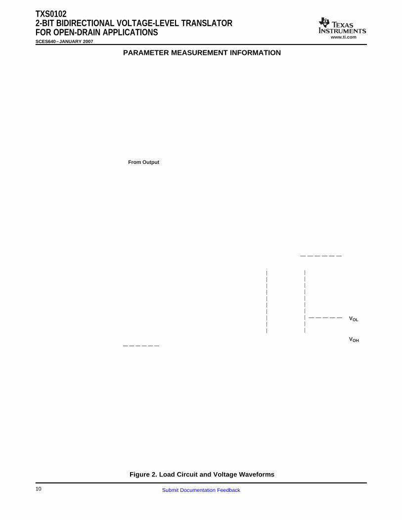
PARAMETER MEASUREMENT INFORMATION
VOH
VOL
From Output Under Test
LOAD CIRCUIT FOR ENABLE/DISABLETIME MEASUREMENT
S1
2 × VCCO
Open
50 k
tPLH tPHL
OutputControl
(low-levelenabling)
OutputWaveform 1
S1 at 2 × VCCO(see Note B)
OutputWaveform 2
S1 at GND(see Note B)
tPZL
tPZH
tPLZ
tPHZ
VCCA/2VCCA/2
VCCI
0 V
VCCO/2VOH
VOL
0 V
0.1 VCCO
VCCO/2
0.9 VCCOVCCO/2
0 V
VCCI
0 V
VCCI/2 VCCI/2
tw
Input
VCCA
VCCO
VOLTAGE WAVEFORMSPROPAGATION DELAY TIMES
VOLTAGE WAVEFORMSPULSE DURATION
VOLTAGE WAVEFORMSENABLE AND DISABLE TIMES
Output
Input
tPZL/tPLZtPHZ/tPZH
2 × VCCOOpen
TEST S1
NOTES: A. CL includes probe and jig capacitance.B. Waveform 1 is for an output with internal conditions such that the output is low, except when disabled by the output control.
Waveform 2 is for an output with internal conditions such that the output is high, except when disabled by the output control.C. All input pulses are supplied by generators having the following characteristics: PRR10 MHz, ZO = 50 Ω, dv/dt ≥ 1 V/ns.D. The outputs are measured one at a time, with one transition per measurement.E. tPLZ and tPHZ are the same as tdis.F. tPZL and tPZH are the same as ten.G. tPLH and tPHL are the same as tpd.H. VCCI is the VCC associated with the input port.I. VCCO is the VCC associated with the output port.J. All parameters and waveforms are not applicable to all devices.
50 k
1 M15 pF
15 pF
DATA RATE, PULSE DURATION, PROPAGATION DELAY,OUTPUT RISE AND FALL TIME MEASUREMENT USING
A PUSH-PULL DRIVER
VCCOVCCI
DUT
IN OUT
1 M15 pF
DATA RATE, PULSE DURATION, PROPAGATION DELAY,OUTPUT RISE AND FALL TIME MEASUREMENT USING
AN OPEN-DRAIN DRIVER
VCCOVCCI
DUT
IN OUT
VCCO/2 VCCO/2
0.9 VCCOVCCO/2
tr
0.1 VCCO
tf
TXS01022-BIT BIDIRECTIONAL VOLTAGE-LEVEL TRANSLATORFOR OPEN-DRAIN APPLICATIONSSCES640–JANUARY 2007
Figure 2. Load Circuit and Voltage Waveforms
10 Submit Documentation Feedback

PACKAGING INFORMATION
Orderable Device Status (1) PackageType
PackageDrawing
Pins PackageQty
Eco Plan (2) Lead/Ball Finish MSL Peak Temp (3)
TXS0102DCTR ACTIVE SM8 DCT 8 3000 Green (RoHS &no Sb/Br)
CU NIPDAU Level-1-260C-UNLIM
TXS0102DCTRE4 ACTIVE SM8 DCT 8 3000 Green (RoHS &no Sb/Br)
CU NIPDAU Level-1-260C-UNLIM
TXS0102DCTT ACTIVE SM8 DCT 8 250 Green (RoHS &no Sb/Br)
CU NIPDAU Level-1-260C-UNLIM
TXS0102DCTTE4 ACTIVE SM8 DCT 8 250 Green (RoHS &no Sb/Br)
CU NIPDAU Level-1-260C-UNLIM
TXS0102DCUR ACTIVE US8 DCU 8 3000 Green (RoHS &no Sb/Br)
CU NIPDAU Level-1-260C-UNLIM
TXS0102DCURG4 ACTIVE US8 DCU 8 3000 Green (RoHS &no Sb/Br)
CU NIPDAU Level-1-260C-UNLIM
TXS0102DCUT ACTIVE US8 DCU 8 250 Green (RoHS &no Sb/Br)
CU NIPDAU Level-1-260C-UNLIM
TXS0102DCUTG4 ACTIVE US8 DCU 8 250 Green (RoHS &no Sb/Br)
CU NIPDAU Level-1-260C-UNLIM
TXS0102YZPR ACTIVE WCSP YZP 8 3000 Green (RoHS &no Sb/Br)
SNAGCU Level-1-260C-UNLIM
(1) The marketing status values are defined as follows:ACTIVE: Product device recommended for new designs.LIFEBUY: TI has announced that the device will be discontinued, and a lifetime-buy period is in effect.NRND: Not recommended for new designs. Device is in production to support existing customers, but TI does not recommend using this part ina new design.PREVIEW: Device has been announced but is not in production. Samples may or may not be available.OBSOLETE: TI has discontinued the production of the device.
(2) Eco Plan - The planned eco-friendly classification: Pb-Free (RoHS), Pb-Free (RoHS Exempt), or Green (RoHS & no Sb/Br) - please checkhttp://www.ti.com/productcontent for the latest availability information and additional product content details.TBD: The Pb-Free/Green conversion plan has not been defined.Pb-Free (RoHS): TI's terms "Lead-Free" or "Pb-Free" mean semiconductor products that are compatible with the current RoHS requirementsfor all 6 substances, including the requirement that lead not exceed 0.1% by weight in homogeneous materials. Where designed to be solderedat high temperatures, TI Pb-Free products are suitable for use in specified lead-free processes.Pb-Free (RoHS Exempt): This component has a RoHS exemption for either 1) lead-based flip-chip solder bumps used between the die andpackage, or 2) lead-based die adhesive used between the die and leadframe. The component is otherwise considered Pb-Free (RoHScompatible) as defined above.Green (RoHS & no Sb/Br): TI defines "Green" to mean Pb-Free (RoHS compatible), and free of Bromine (Br) and Antimony (Sb) based flameretardants (Br or Sb do not exceed 0.1% by weight in homogeneous material)
(3) MSL, Peak Temp. -- The Moisture Sensitivity Level rating according to the JEDEC industry standard classifications, and peak soldertemperature.
Important Information and Disclaimer:The information provided on this page represents TI's knowledge and belief as of the date that it isprovided. TI bases its knowledge and belief on information provided by third parties, and makes no representation or warranty as to theaccuracy of such information. Efforts are underway to better integrate information from third parties. TI has taken and continues to takereasonable steps to provide representative and accurate information but may not have conducted destructive testing or chemical analysis onincoming materials and chemicals. TI and TI suppliers consider certain information to be proprietary, and thus CAS numbers and other limitedinformation may not be available for release.
In no event shall TI's liability arising out of such information exceed the total purchase price of the TI part(s) at issue in this document sold by TIto Customer on an annual basis.
PACKAGE OPTION ADDENDUM
www.ti.com 6-Dec-2007
Addendum-Page 1
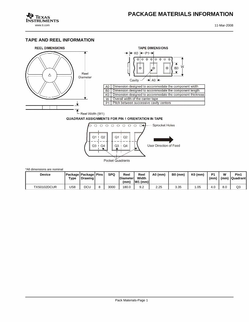
TAPE AND REEL INFORMATION
*All dimensions are nominal
Device PackageType
PackageDrawing
Pins SPQ ReelDiameter
(mm)
ReelWidth
W1 (mm)
A0 (mm) B0 (mm) K0 (mm) P1(mm)
W(mm)
Pin1Quadrant
TXS0102DCUR US8 DCU 8 3000 180.0 9.2 2.25 3.35 1.05 4.0 8.0 Q3
PACKAGE MATERIALS INFORMATION
www.ti.com 11-Mar-2008
Pack Materials-Page 1
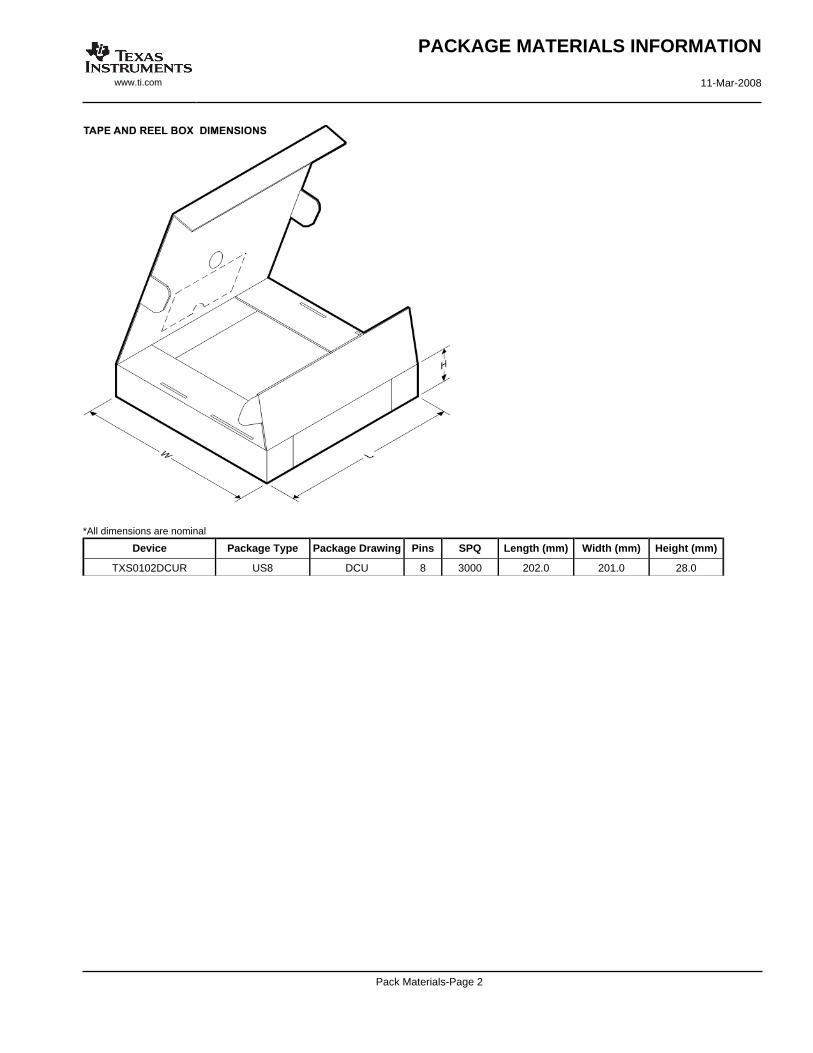
*All dimensions are nominal
Device Package Type Package Drawing Pins SPQ Length (mm) Width (mm) Height (mm)
TXS0102DCUR US8 DCU 8 3000 202.0 201.0 28.0
PACKAGE MATERIALS INFORMATION
www.ti.com 11-Mar-2008
Pack Materials-Page 2

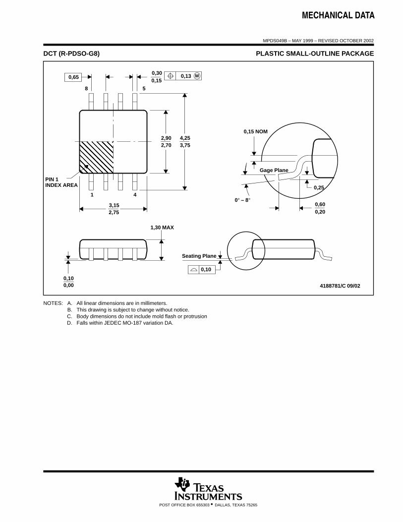
MECHANICAL DATA
MPDS049B – MAY 1999 – REVISED OCTOBER 2002
POST OFFICE BOX 655303 • DALLAS, TEXAS 75265
DCT (R-PDSO-G8) PLASTIC SMALL-OUTLINE PACKAGE
ÇÇÇÇÇÇÇÇÇÇÇÇÇÇÇÇÇÇÇÇ
0,600,20
0,25
0° – 8°
0,15 NOM
Gage Plane
4188781/C 09/02
4,25
5
0,300,15
2,903,752,70
8
4
3,152,75
1
0,100,00
1,30 MAX
Seating Plane
0,10
M0,130,65
PIN 1INDEX AREA
NOTES: A. All linear dimensions are in millimeters.B. This drawing is subject to change without notice.C. Body dimensions do not include mold flash or protrusionD. Falls within JEDEC MO-187 variation DA.

IMPORTANT NOTICETexas Instruments Incorporated and its subsidiaries (TI) reserve the right to make corrections, modifications, enhancements, improvements,and other changes to its products and services at any time and to discontinue any product or service without notice. Customers shouldobtain the latest relevant information before placing orders and should verify that such information is current and complete. All products aresold subject to TI’s terms and conditions of sale supplied at the time of order acknowledgment.TI warrants performance of its hardware products to the specifications applicable at the time of sale in accordance with TI’s standardwarranty. Testing and other quality control techniques are used to the extent TI deems necessary to support this warranty. Except wheremandated by government requirements, testing of all parameters of each product is not necessarily performed.TI assumes no liability for applications assistance or customer product design. Customers are responsible for their products andapplications using TI components. To minimize the risks associated with customer products and applications, customers should provideadequate design and operating safeguards.TI does not warrant or represent that any license, either express or implied, is granted under any TI patent right, copyright, mask work right,or other TI intellectual property right relating to any combination, machine, or process in which TI products or services are used. Informationpublished by TI regarding third-party products or services does not constitute a license from TI to use such products or services or awarranty or endorsement thereof. Use of such information may require a license from a third party under the patents or other intellectualproperty of the third party, or a license from TI under the patents or other intellectual property of TI.Reproduction of TI information in TI data books or data sheets is permissible only if reproduction is without alteration and is accompaniedby all associated warranties, conditions, limitations, and notices. Reproduction of this information with alteration is an unfair and deceptivebusiness practice. TI is not responsible or liable for such altered documentation. Information of third parties may be subject to additionalrestrictions.Resale of TI products or services with statements different from or beyond the parameters stated by TI for that product or service voids allexpress and any implied warranties for the associated TI product or service and is an unfair and deceptive business practice. TI is notresponsible or liable for any such statements.TI products are not authorized for use in safety-critical applications (such as life support) where a failure of the TI product would reasonablybe expected to cause severe personal injury or death, unless officers of the parties have executed an agreement specifically governingsuch use. Buyers represent that they have all necessary expertise in the safety and regulatory ramifications of their applications, andacknowledge and agree that they are solely responsible for all legal, regulatory and safety-related requirements concerning their productsand any use of TI products in such safety-critical applications, notwithstanding any applications-related information or support that may beprovided by TI. Further, Buyers must fully indemnify TI and its representatives against any damages arising out of the use of TI products insuch safety-critical applications.TI products are neither designed nor intended for use in military/aerospace applications or environments unless the TI products arespecifically designated by TI as military-grade or "enhanced plastic." Only products designated by TI as military-grade meet militaryspecifications. Buyers acknowledge and agree that any such use of TI products which TI has not designated as military-grade is solely atthe Buyer's risk, and that they are solely responsible for compliance with all legal and regulatory requirements in connection with such use.TI products are neither designed nor intended for use in automotive applications or environments unless the specific TI products aredesignated by TI as compliant with ISO/TS 16949 requirements. Buyers acknowledge and agree that, if they use any non-designatedproducts in automotive applications, TI will not be responsible for any failure to meet such requirements.Following are URLs where you can obtain information on other Texas Instruments products and application solutions:Products ApplicationsAmplifiers amplifier.ti.com Audio www.ti.com/audioData Converters dataconverter.ti.com Automotive www.ti.com/automotiveDSP dsp.ti.com Broadband www.ti.com/broadbandClocks and Timers www.ti.com/clocks Digital Control www.ti.com/digitalcontrolInterface interface.ti.com Medical www.ti.com/medicalLogic logic.ti.com Military www.ti.com/militaryPower Mgmt power.ti.com Optical Networking www.ti.com/opticalnetworkMicrocontrollers microcontroller.ti.com Security www.ti.com/securityRFID www.ti-rfid.com Telephony www.ti.com/telephonyRF/IF and ZigBee® Solutions www.ti.com/lprf Video & Imaging www.ti.com/video
Wireless www.ti.com/wireless
Mailing Address: Texas Instruments, Post Office Box 655303, Dallas, Texas 75265Copyright © 2008, Texas Instruments Incorporated


![10393 (C) Elphel, Inc. 2015 · ppad 6 vin 4 en 3 fault 1 vout u29 txs0101drlr 3 a 2 gnd 5 oe 1 vcca 6 vccb 4 b u28 ... led_act 2 lx 39 mdio 7 rset 10 trdm[0] 13 trdm[1] 16 trdm[2]](https://img.dokumen.tips/doc/110x75/5b41bb3e7f8b9ad0088b565d/10393-c-elphel-inc-2015-ppad-6-vin-4-en-3-fault-1-vout-u29-txs0101drlr-3.jpg)


![Wireless Starter Kit Mainboard - Silicon Labs · vcom_enable pti0[0..2] vmcu gnd gnd gnd gnd vmcu vrf 5v 3v3 gnd vrf gnd gnd gnd gnd gnd usb_vbus usb_vreg usb_vbus 5v 5v_dbg …](https://img.dokumen.tips/doc/110x75/5ac0fbea7f8b9a4e7c8c7c14/wireless-starter-kit-mainboard-silicon-labs-pti002-vmcu-gnd-gnd-gnd-gnd-vmcu.jpg)