Embed Size (px)
Citation preview

TTM Technologies Flex Webinar
2015

Agenda
• Flex 101
• Material Options
• Flex Design Guidelines
• Cost Drivers
• Flex & Rigid Flex Support Strategy
• Application Examples
• IPC 6013 Updates
• Q&A
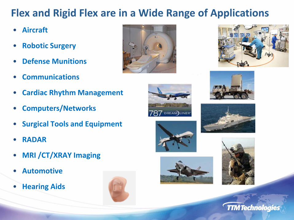
Flex and Rigid Flex are in a Wide Range of Applications
• Aircraft
• Robotic Surgery
• Defense Munitions
• Communications
• Cardiac Rhythm Management
• Computers/Networks
• Surgical Tools and Equipment
• RADAR
• MRI /CT/XRAY Imaging
• Automotive
• Hearing Aids

Flex & Rigid-Flex Technology
Advantages:
• Enabling Technology for New Generation of Products
• Increased Reliability via Reduced Interconnection
• Increase Functionality / Less Space
• A Single Substrate for Electronic System Packaging
• System Component Reduction / Assembly Operations
• Improved Signal Integrity / Impedance Performance
• Provide for a Smaller, Lighter & Reliable Product
As manufactured-Flat condition
Inside Metal Housing Bracket
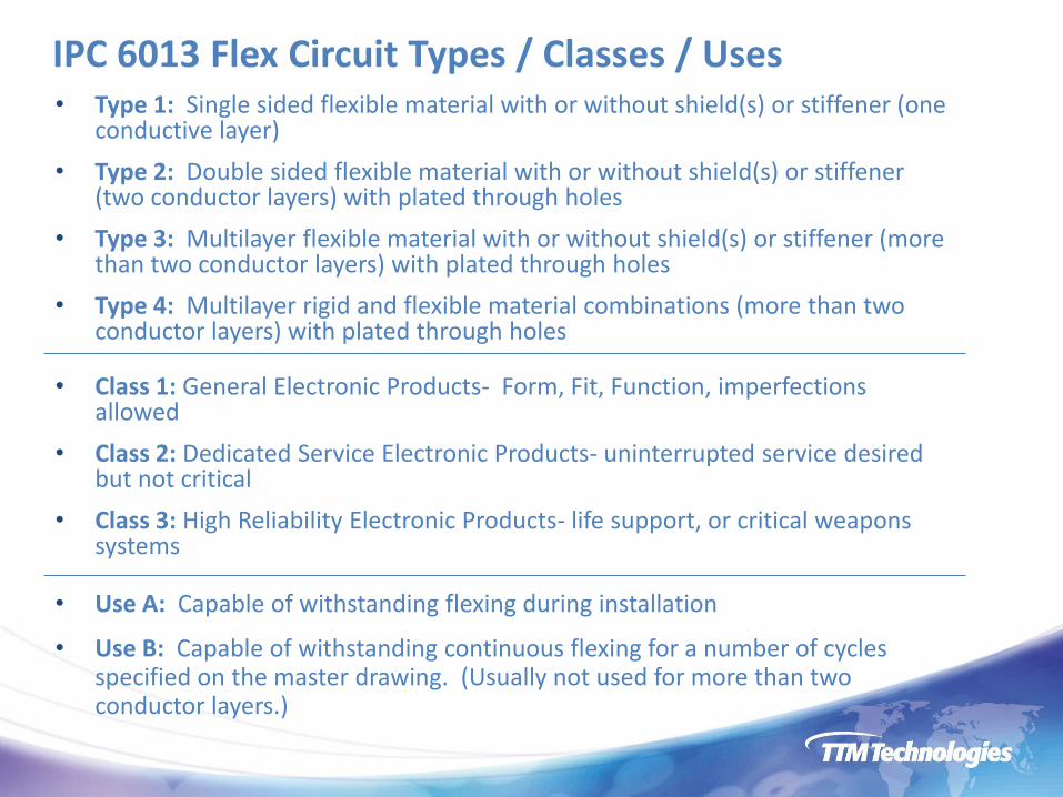
IPC 6013 Flex Circuit Types / Classes / Uses • Type 1: Single sided flexible material with or without shield(s) or stiffener (one
conductive layer)
• Type 2: Double sided flexible material with or without shield(s) or stiffener (two conductor layers) with plated through holes
• Type 3: Multilayer flexible material with or without shield(s) or stiffener (more than two conductor layers) with plated through holes
• Type 4: Multilayer rigid and flexible material combinations (more than two conductor layers) with plated through holes
• Class 1: General Electronic Products- Form, Fit, Function, imperfections allowed
• Class 2: Dedicated Service Electronic Products- uninterrupted service desired but not critical
• Class 3: High Reliability Electronic Products- life support, or critical weapons systems
• Use A: Capable of withstanding flexing during installation
• Use B: Capable of withstanding continuous flexing for a number of cycles specified on the master drawing. (Usually not used for more than two conductor layers.)
Flex Specification / Material Used
Fabrication Specifications • IPC-6013 Class I, II, III • Mil-P-50884
Flex Material Designations (.001” to .006”) • IPC-4204/11; Metal Clad Dielectrics –Adhesive less Polyimide • IPC-4204/1 ;Metal Clad Dielectrics with Acrylic Adhesive • IPC-4203/1(Adhesive Coated Dielectric Films) Coverlay and Bond Ply • IPC-4203/18 (Bonding Sheet Adhesive)
(* All DuPont Products)
Rigid Material Designations (.003” to .125”) • IPC-4101/24, /26 Epoxy Rigid cores & No-Flow pre-pregs (≥170Tg) • IPC-4101/40, /41 , /42 Polyimide Rigid cores & No-Flow pre-pregs (≥200Tg)
• (Other core materials can be used but no-flow is limited to polyimide & epoxy only)

Rigid Material Summary – Dk/Df Comparison (2Ghz) 4.4 4.4 4.4
4.24.1 4.1 4.0 4.0
3.9 3.9
3.8 3.8 3.8 3.7 3.73.6 3.6
0.0
0.5
1.0
1.5
2.0
2.5
3.0
3.5
4.0
4.5
5.0
R-1755V R-2125 TU-862HF EL190T EM-370(D) Meg 2 370HR 185HR FR406 Theta IS415 Meg 4 TU-
872SLK
FR408HR N4000 -13 IT 150DA Meg 6
Dk (@ 2GHz)
• DuPont AP material Dk ≈3.3 0.021
0.017 0.017
0.016
0.013 0.013 0.013
0.012
0.011 0.011
0.009 0.009 0.009
0.008
0.005 0.005
0.004
0.002
0
0.002
0.004
0.006
0.008
0.01
0.012
0.014
0.016
0.018
0.02
0.022
370HR FR406 185HR R-1755V EM-
370(D)
IS415 TU-
862HF
R-2125 EL190T Meg 2 FR408HR N4000 -
13
Theta TU-
872SLK
Meg 4 IT 150DA FX-II Meg 6
Df (@ 2 GHz)
• DuPont AP material Df ≈0.003

Flex & Rigid-Flex Circuit Design Guidelines

Rigid Flex Stack Example
Un-bonded flex layers can bend at tighter radius
Approx .0025 of prepreg is required to bond each oz. of copper layer without lamination voids
Minimum of .001 coverlay adhesive is required to encapsulate 1 oz. of copper
Provide option to add non-functional pads to prevent lamination voids
Covers Cut back in rigid section for maximum via reliability
Example 8 layer Rigid Flex: 4 rigid and 4 flexible layers
Soft Epoxy provides strain relief at rigid to flex transition (.020-.100”)

Flex Areas
Minimum Bend Radius (R=(c/2) {(100-Eb)/Eb]-D)
Calculated Values:
• Single Sided:
• R/T=.09 for One time crease
• R/T=.45 for Flex to install
• R/T=31 for Dynamic flex
• Double Sided:
• R/T=1.16 for One time crease
• R/T=2.15 for Flex to install
• R/T=88 for Dynamic flex
• Safe Rule of Thumb:
• 10:1 Single & Double sided circuits
• 20:1 Multilayer circuits
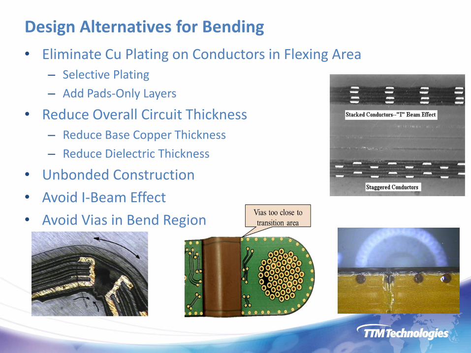
Design Alternatives for Bending
• Eliminate Cu Plating on Conductors in Flexing Area – Selective Plating
– Add Pads-Only Layers
• Reduce Overall Circuit Thickness – Reduce Base Copper Thickness
– Reduce Dielectric Thickness
• Unbonded Construction
• Avoid I-Beam Effect
• Avoid Vias in Bend Region

Ground Plane Options
• Solid Ground Plane – Selectively apply solid copper plane if possible
• Cross Hatch Pattern – Have pattern at an angle to bend
• Silver Epoxy – More flexible than copper
– Adds operations to flow
• For more flexibility, consider using thinner copper for ground planes - Design and application dependent

Bonded vs. Un-bonded Flexible Layers
• Smaller and tighter bend radius possible
• Impedance impact
• Bend memory
• Cost impact - number of materials and processes
• Beware of “pucker” effect
Five flex substrates Three flex substrates Bonded flex layers

Stagger Flexible Layers to Maximize Flexibility
• Allows for much tighter bend radius

Flexibility vs. Impedance Case Study
Problem:
• Impedance drove thick dielectric
• Four solid planes make part stiffer
• Part requires tight bend in short flex
• Requires forming tooling to bend
Solution(s):
• Cross hatch shielding to allow thinner dielectric & better flexibility
• Possible conversion to TK material – Thinner and more flexible

Bookbinder Technology – When bend is very tight
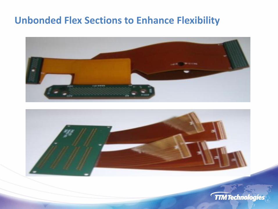
Unbonded Flex Sections to Enhance Flexibility
HDI Flex & Rigid Flex
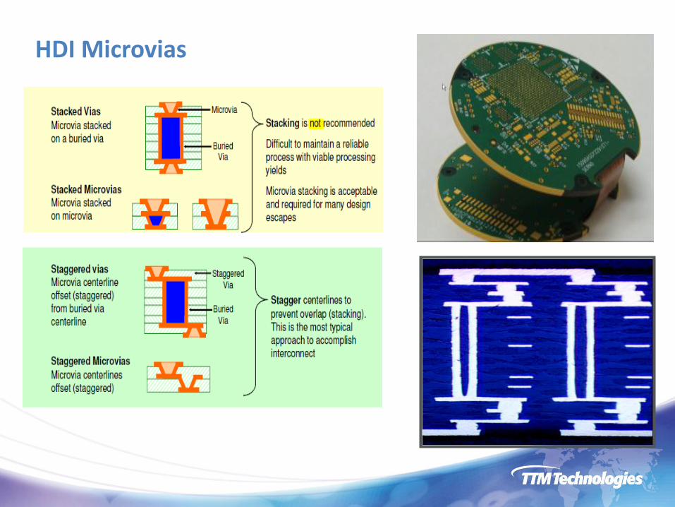
HDI Microvias

HDI Common Structures
TTM Proprietary and Confidential 20

Laser Microvia Model - Feature Pitch 0.8 mm (31.5 mils)
TTM Proprietary and Confidential 21
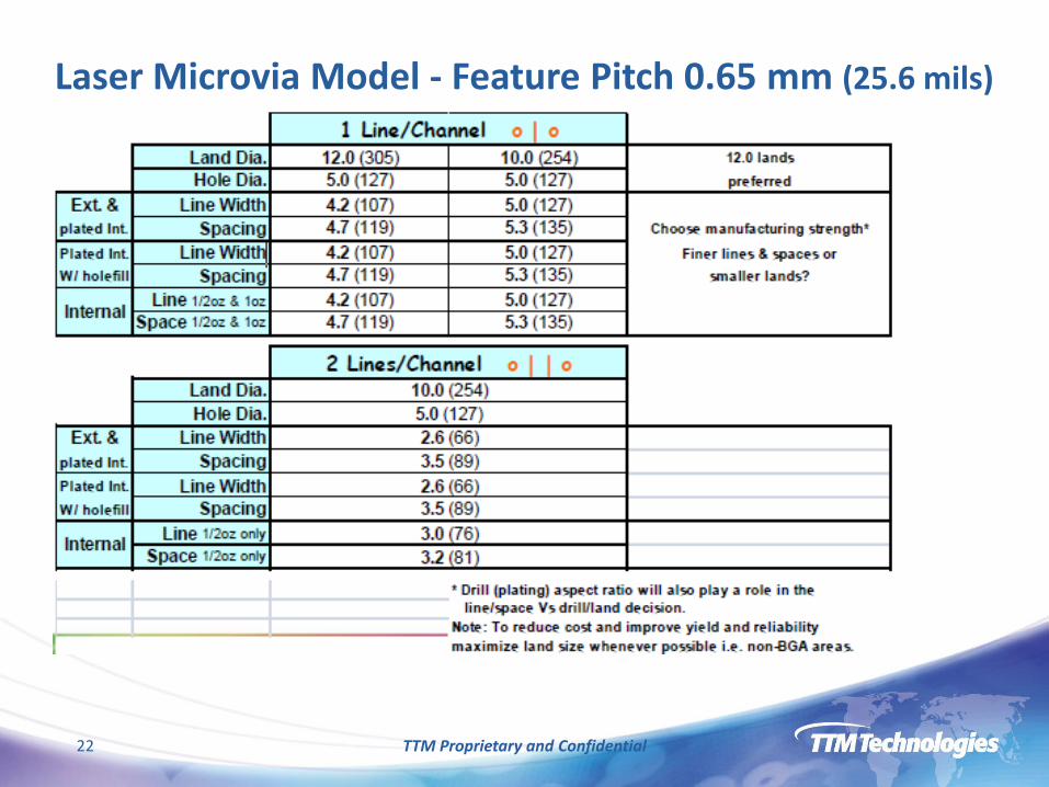
Laser Microvia Model - Feature Pitch 0.65 mm (25.6 mils)
TTM Proprietary and Confidential 22

Laser Microvia Model - Feature Pitch 0.5 mm (19.7 mils)
TTM Proprietary and Confidential 23

Via In Pad
• Technology Drivers for VIPPO: • Interconnect Applications using Hole fill • Processing Steps for VIPPO products • IPC Wrap Plating Specification Review (Required for VIPPO) • Design Guidelines when Implementing VIPPO into Designs

Benefits in Design and Assembly

Via in Pad Manufacturing Flow

Overview of Wrap Plating Specification

Wrap and Surface Copper – Class 2 Example

Plated Wrap Design Guidelines

Wrap Plated Layer Design Guidelines
• Localized BGA escape spacing can be reduced (neck downs) but increasing frequency - quantity will begin to reduce yield
• Maximum of 3/8 oz or ¼ oz foil required on all wrap plated layers
• Allow copper thieving on all layers – internal and external to improve: – Plating thickness distribution
– Overall board thickness variation (improved planarization)
• Don’t forget about plated sub laminated internal layers like blind via stopping layers, buried vias require the same considerations because they are effectively what is normally considered an “external layer”.
• Add a drawing note: All XX mil vias to be non conductively filled and copper capped to enable direct bonding.
TTM Proprietary and Confidential 30

Flex & Rigid Flex Cost and DFM Considerations

Cost Drivers – Material Utilization
• Typical manufacturing panel is 18” x 24”
• Useable Panel Area is reduced by:
– Coupons
– Tooling Holes
– Border
– Useable space is 16.5”x 22.5”
• Design pallet to easily nest with minimal scrap
Note:
Evaluation / Impedance coupons must be inside useable areas.

Common Design Issues Impacting Cost and Lead Time
Data Package/Documentation issues
• Print dimensions do not match the data
• Pre-approved stack-up doesn’t match requirements in data
• Drill file hole counts do not match drill table on drawing
CAD Data issues
• Addition of teardrops at pad to circuit junction
• Pad sizes not designed to achieve desired annular ring
• Hole2Cu violations
• Soldermask via plugging, capping, tenting, encroaching, post plugging clarifications
• S/M web widths below minimum (depends on mask type/color)
• Silkscreen encroachment on exposed pads

Materials Matter – Flex Substrates
• Flex Laminates are 2.5-10X the cost of rigid laminates
• .002” ( 50um) dielectric is most common
• 1 Oz (35um) copper is lowest cost
• Cost is most sensitive to Kapton thickness
• Unbalanced constructions may have lead time issues due to lower on hand inventory
Most Common Rigid Laminate
Most Common Laminate

Product Examples

Structure: 2L FPCs
With FR4, PI stiffener, PSA
Assembly Ready
Flex Product Snapshot – Type Two Circuits

SMT Assembly on Flex Using Stiffeners
Key Features:
Shipped in pallet for SMT Assembly
Stiffener material doubles as the pallet
Applied with thermoset adhesive or PSA

Flex Assembly Product
• Flex & Rigid-Flex assembly examples
IPC 6013 Rev C Key Updates
IPC 6013 Rev C Key Updates
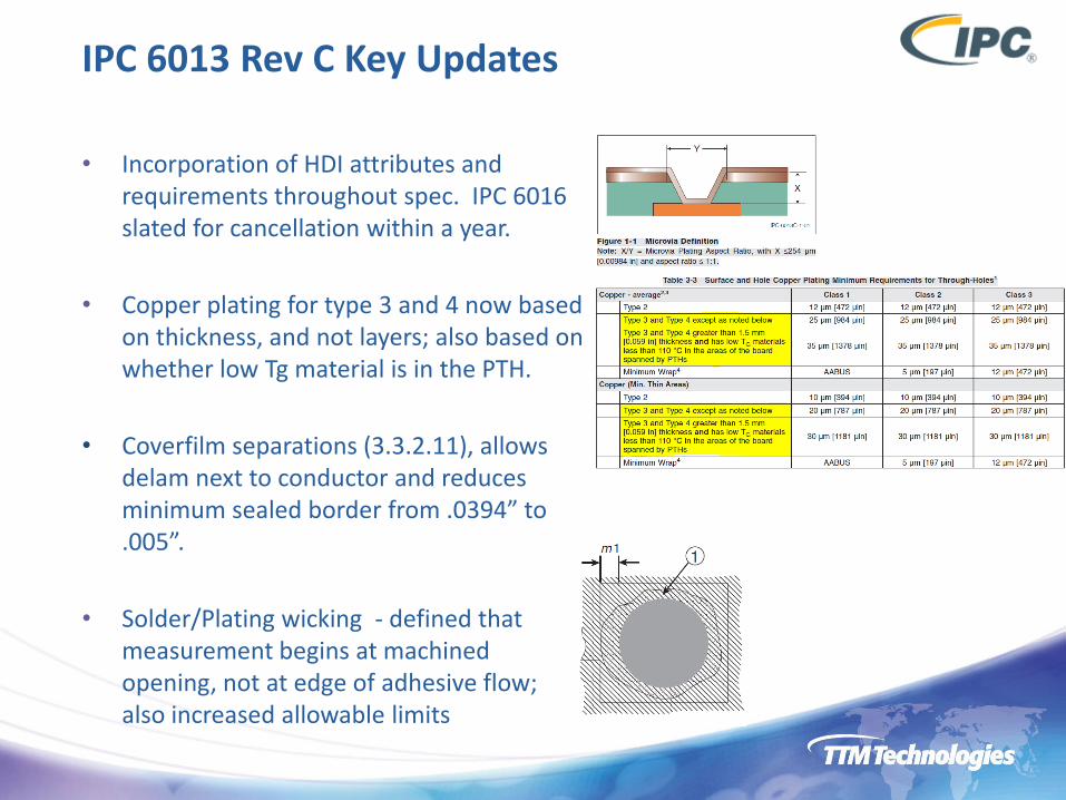
• Incorporation of HDI attributes and requirements throughout spec. IPC 6016 slated for cancellation within a year.
• Copper plating for type 3 and 4 now based on thickness, and not layers; also based on whether low Tg material is in the PTH.
• Coverfilm separations (3.3.2.11), allows delam next to conductor and reduces minimum sealed border from .0394” to .005”.
• Solder/Plating wicking - defined that measurement begins at machined opening, not at edge of adhesive flow; also increased allowable limits

IPC 6013 Rev C Key Updates
• Eliminated void limits between circuits and stiffeners
• Allows Mfr insertion of tooling holes, fiducials and coupons into arrays unless directed otherwise by customer
• Class 1 and 2 spacing reduction is now 30%, not 50% See table 3-14

IPC 6013 Rev C Key Updates
• Non Functional pads cannot be removed without customer approval
• Multiple Thermal Stress Test methods now exist based on material selection and multiple reflows
• The thermal Zone evaluation was reworded extensively – Is it clearer? Maybe…
IPC 6013 Rev C Key Updates
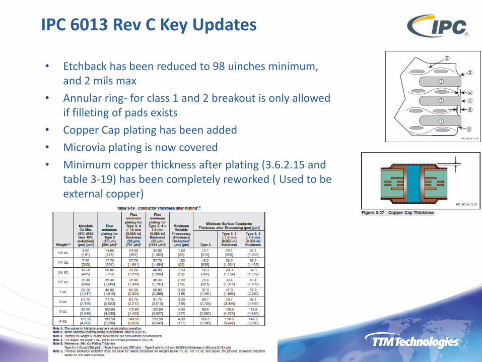
• Etchback has been reduced to 98 uinches minimum, and 2 mils max
• Annular ring- for class 1 and 2 breakout is only allowed if filleting of pads exists
• Copper Cap plating has been added
• Microvia plating is now covered
• Minimum copper thickness after plating (3.6.2.15 and table 3-19) has been completely reworked ( Used to be external copper)

Thank you!