Embed Size (px)
Citation preview

TTThhheee LLLeeeaaadddiiinnnggg PPPrrrooovvviiidddeeerrr ooofff
HHHiiiggghhh---PPPeeerrrfffooorrrmmmaaannnccceee
SSSiiillliiicccooonnn---PPPrrrooovvveeennn
MMMiiixxxeeeddd---SSSiiigggnnnaaalll IIIPPP
BENEFITS
Integrate Mixed-Signal Content into Your SoC
Improve Performance
Reduce Power Dissipation
Accelerate Time-to-Market
Reduce Design Costs & Risk
Mixed Signal IP Design Guide
Vol13 Iss2 v3, Nov. 5, 2013
© 2013 Silicon & Software Systems Ltd. All rights reserved.
For more detailed information regarding the S3 Group’s Mixed Signal IP portfolio please visit www.s3group.com/silicon

Mixed Signal IP Design Guide from S3 Group The information contained herein is for promotional and technical guideline purposes only. No license is granted, either by implication or otherwise, under any intellectual property rights of S3 Group.
© 2013 Silicon & Software Systems Ltd. All rights reserved. Page 2
RF IPs – All Nodes ....................................................................................................................................... 3
Analog-Baseband – All Nodes ..................................................................................................................... 4
Analog Front-Ends (AFE) – All Nodes ....................................................................................................... 4
SAR and Sigma-Delta Analog-to-Digital Converters (ADC) – All Nodes ............................................... 5
Pipeline Analog-to-Digital Converters (ADC) – 40nm Node .................................................................... 6
Pipeline Analog-to-Digital Converters (ADC) – 65nm & 55nm Nodes ................................................... 7
Pipeline Analog-to-Digital Converters (ADC) – 65nm & 55nm Nodes (cont.) ....................................... 8
Pipeline Analog-to-Digital Converters (ADC) – 90nm Node .................................................................... 9
Pipeline Analog-to-Digital Converters (ADC) – 0.13um Node ................................................................. 9
Pipeline Analog-to-Digital Converters (ADC) – 0.18um Node ............................................................... 10
Temperature Sensors and Temperature to Digital Converters – All Nodes ......................................... 10
Digital-to-Analog Converters (DAC) – 40m Node ................................................................................... 11
Digital-to-Analog Converters (DAC) – 65m & 55nm Nodes .................................................................. 11
Digital-to-Analog Converters (DAC) – 90nm Node ................................................................................ 12
Digital-to-Analog Converters (DAC) – 0.13um Node ............................................................................. 12
Digital-to-Analog Converters (DAC) – 0.18um Node ............................................................................. 12
Phase-Locked Loops (PLL) – All Nodes ................................................................................................... 13
Power Management Platform ................................................................................................................... 14
Power Management: DC-DC Converters – All Nodes ............................................................................ 14
Power Management: Miscellaneous – All Nodes ..................................................................................... 14
Power Management: LDOs – All Nodes ................................................................................................... 15
Mixed Signal IP Design Guide from S3 Group The information contained herein is for promotional and technical guideline purposes only. No license is granted, either by implication or otherwise, under any intellectual property rights of S3 Group.
© 2013 Silicon & Software Systems Ltd. All rights reserved. Page 3
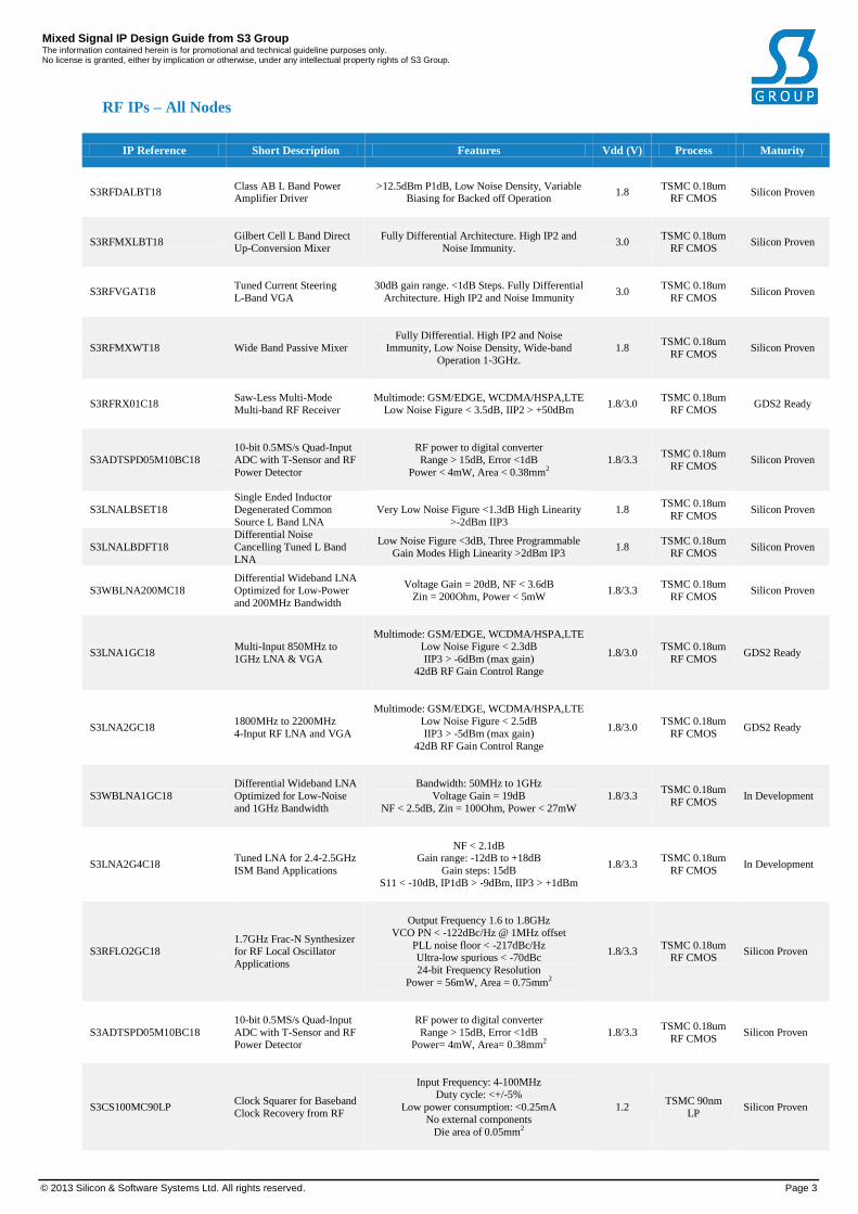
RF IPs – All Nodes
IP Reference Short Description Features Vdd (V) Process Maturity
S3RFDALBT18 Class AB L Band Power Amplifier Driver
>12.5dBm P1dB, Low Noise Density, Variable Biasing for Backed off Operation
1.8 TSMC 0.18um
RF CMOS Silicon Proven
S3RFMXLBT18 Gilbert Cell L Band Direct
Up-Conversion Mixer
Fully Differential Architecture. High IP2 and
Noise Immunity.
3.0 TSMC 0.18um
RF CMOS Silicon Proven
S3RFVGAT18 Tuned Current Steering
L-Band VGA
30dB gain range. <1dB Steps. Fully Differential
Architecture. High IP2 and Noise Immunity
3.0 TSMC 0.18um
RF CMOS Silicon Proven
S3RFMXWT18 Wide Band Passive Mixer
Fully Differential. High IP2 and Noise
Immunity, Low Noise Density, Wide-band
Operation 1-3GHz.
1.8 TSMC 0.18um
RF CMOS Silicon Proven
S3RFRX01C18 Saw-Less Multi-Mode
Multi-band RF Receiver
Multimode: GSM/EDGE, WCDMA/HSPA,LTE
Low Noise Figure < 3.5dB, IIP2 > +50dBm
1.8/3.0 TSMC 0.18um
RF CMOS GDS2 Ready
S3ADTSPD05M10BC18
10-bit 0.5MS/s Quad-Input
ADC with T-Sensor and RF
Power Detector
RF power to digital converter
Range > 15dB, Error <1dB
Power < 4mW, Area < 0.38mm2
1.8/3.3 TSMC 0.18um
RF CMOS Silicon Proven
S3LNALBSET18
Single Ended Inductor
Degenerated Common
Source L Band LNA
Very Low Noise Figure <1.3dB High Linearity
>-2dBm IIP3
1.8 TSMC 0.18um
RF CMOS Silicon Proven
S3LNALBDFT18
Differential Noise
Cancelling Tuned L Band
LNA
Low Noise Figure <3dB, Three Programmable
Gain Modes High Linearity >2dBm IP3 1.8
TSMC 0.18um
RF CMOS Silicon Proven
S3WBLNA200MC18
Differential Wideband LNA
Optimized for Low-Power
and 200MHz Bandwidth
Voltage Gain = 20dB, NF < 3.6dB
Zin = 200Ohm, Power < 5mW
1.8/3.3 TSMC 0.18um
RF CMOS Silicon Proven
S3LNA1GC18 Multi-Input 850MHz to
1GHz LNA & VGA
Multimode: GSM/EDGE, WCDMA/HSPA,LTE
Low Noise Figure < 2.3dB
IIP3 > -6dBm (max gain) 42dB RF Gain Control Range
1.8/3.0 TSMC 0.18um
RF CMOS GDS2 Ready
S3LNA2GC18 1800MHz to 2200MHz
4-Input RF LNA and VGA
Multimode: GSM/EDGE, WCDMA/HSPA,LTE
Low Noise Figure < 2.5dB
IIP3 > -5dBm (max gain)
42dB RF Gain Control Range
1.8/3.0 TSMC 0.18um
RF CMOS GDS2 Ready
S3WBLNA1GC18
Differential Wideband LNA
Optimized for Low-Noise
and 1GHz Bandwidth
Bandwidth: 50MHz to 1GHz
Voltage Gain = 19dB
NF < 2.5dB, Zin = 100Ohm, Power < 27mW
1.8/3.3 TSMC 0.18um
RF CMOS In Development
S3LNA2G4C18 Tuned LNA for 2.4-2.5GHz
ISM Band Applications
NF < 2.1dB Gain range: -12dB to +18dB
Gain steps: 15dB
S11 < -10dB, IP1dB > -9dBm, IIP3 > +1dBm
1.8/3.3 TSMC 0.18um
RF CMOS In Development
S3RFLO2GC18 1.7GHz Frac-N Synthesizer for RF Local Oscillator
Applications
Output Frequency 1.6 to 1.8GHz
VCO PN < -122dBc/Hz @ 1MHz offset
PLL noise floor < -217dBc/Hz Ultra-low spurious < -70dBc
24-bit Frequency Resolution
Power = 56mW, Area = 0.75mm2
1.8/3.3 TSMC 0.18um
RF CMOS Silicon Proven
S3ADTSPD05M10BC18
10-bit 0.5MS/s Quad-Input
ADC with T-Sensor and RF Power Detector
RF power to digital converter
Range > 15dB, Error <1dB Power= 4mW, Area= 0.38mm
2
1.8/3.3 TSMC 0.18um
RF CMOS Silicon Proven
S3CS100MC90LP Clock Squarer for Baseband
Clock Recovery from RF
Input Frequency: 4-100MHz
Duty cycle: <+/-5%
Low power consumption: <0.25mA
No external components
Die area of 0.05mm2
1.2 TSMC 90nm
LP Silicon Proven
Mixed Signal IP Design Guide from S3 Group The information contained herein is for promotional and technical guideline purposes only. No license is granted, either by implication or otherwise, under any intellectual property rights of S3 Group.
© 2013 Silicon & Software Systems Ltd. All rights reserved. Page 4
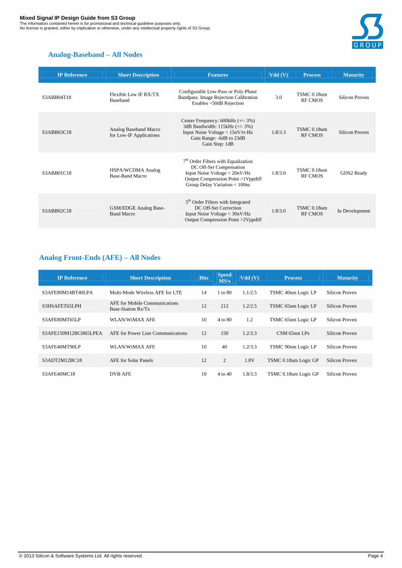
Analog-Baseband – All Nodes
IP Reference Short Description Features Vdd (V) Process Maturity
S3ABB04T18 Flexible Low IF RX/TX
Baseband
Configurable Low-Pass or Poly-Phase
Bandpass. Image Rejection Calibration
Enables ~50dB Rejection
3.0 TSMC 0.18um
RF CMOS Silicon Proven
S3ABB03C18 Analog Baseband Macro
for Low-IF Applications
Center Frequency: 600kHz (+/- 3%)
3dB Bandwidth: 115kHz (+/- 3%)
Input Noise Voltage < 15nV/rt-Hz
Gain Range: -6dB to 23dB
Gain Step: 1dB
1.8/3.3 TSMC 0.18um
RF CMOS Silicon Proven
S3ABB01C18 HSPA/WCDMA Analog
Base-Band Macro
7th
Order Filters with Equalization
DC Off-Set Compensation
Input Noise Voltage < 20nV/Hz
Output Compression Point >1Vppdiff
Group Delay Variation < 100ns
1.8/3.0 TSMC 0.18um
RF CMOS GDS2 Ready
S3ABB02C18 GSM/EDGE Analog Base-
Band Macro
5
th Order Filters with Integrated
DC Off-Set Correction
Input Noise Voltage < 30nV/Hz
Output Compression Point >2Vppdiff
1.8/3.0 TSMC 0.18um
RF CMOS In Development
Analog Front-Ends (AFE) – All Nodes
IP Reference Short Description Bits Speed
MS/s Vdd (V) Process Maturity
S3AFE80M14BT40LPA Multi-Mode Wireless AFE for LTE 14 1 to 80 1.1/2.5 TSMC 40nm Logic LP Silicon Proven
S3HSAFET65LPH AFE for Mobile Communications
Base-Station Rx/Tx 12 212 1.2/2.5 TSMC 65nm Logic LP Silicon Proven
S3AFE80MT65LP WLAN/WiMAX AFE 10 4 to 80 1.2 TSMC 65nm Logic LP Silicon Proven
S3AFE150M12BCH65LPEA AFE for Power Line Communications 12 150 1.2/3.3 CSM 65nm LPe Silicon Proven
S3AFE40MT90LP WLAN/WiMAX AFE 10 40 1.2/3.3 TSMC 90nm Logic LP Silicon Proven
S3ADT2M12BC18 AFE for Solar Panels 12 2 1.8V TSMC 0.18um Logic GP Silicon Proven
S3AFE40MC18 DVB AFE 10 4 to 40 1.8/3.3 TSMC 0.18um Logic GP Silicon Proven
Mixed Signal IP Design Guide from S3 Group The information contained herein is for promotional and technical guideline purposes only. No license is granted, either by implication or otherwise, under any intellectual property rights of S3 Group.
© 2013 Silicon & Software Systems Ltd. All rights reserved. Page 5
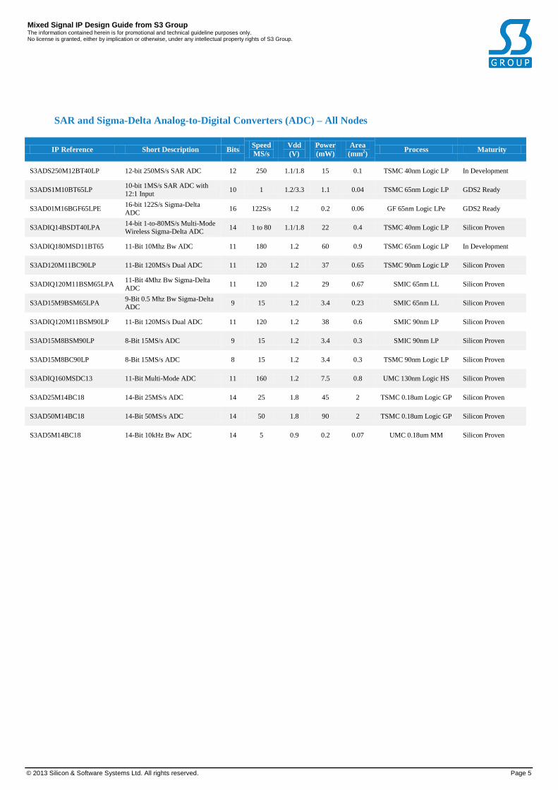
SAR and Sigma-Delta Analog-to-Digital Converters (ADC) – All Nodes
IP Reference Short Description Bits Speed
MS/s
Vdd
(V)
Power
(mW)
Area
(mm2) Process Maturity
S3ADS250M12BT40LP 12-bit 250MS/s SAR ADC 12 250 1.1/1.8 15 0.1 TSMC 40nm Logic LP In Development
S3ADS1M10BT65LP 10-bit 1MS/s SAR ADC with
12:1 Input 10 1 1.2/3.3 1.1 0.04 TSMC 65nm Logic LP GDS2 Ready
S3AD01M16BGF65LPE 16-bit 122S/s Sigma-Delta
ADC 16 122S/s 1.2 0.2 0.06 GF 65nm Logic LPe GDS2 Ready
S3ADIQ14BSDT40LPA 14-bit 1-to-80MS/s Multi-Mode
Wireless Sigma-Delta ADC 14 1 to 80 1.1/1.8 22 0.4 TSMC 40nm Logic LP Silicon Proven
S3ADIQ180MSD11BT65 11-Bit 10Mhz Bw ADC 11 180 1.2 60 0.9 TSMC 65nm Logic LP In Development
S3AD120M11BC90LP 11-Bit 120MS/s Dual ADC 11 120 1.2 37 0.65 TSMC 90nm Logic LP Silicon Proven
S3ADIQ120M11BSM65LPA 11-Bit 4Mhz Bw Sigma-Delta
ADC 11 120 1.2 29 0.67 SMIC 65nm LL Silicon Proven
S3AD15M9BSM65LPA 9-Bit 0.5 Mhz Bw Sigma-Delta
ADC 9 15 1.2 3.4 0.23 SMIC 65nm LL Silicon Proven
S3ADIQ120M11BSM90LP 11-Bit 120MS/s Dual ADC 11 120 1.2 38 0.6 SMIC 90nm LP Silicon Proven
S3AD15M8BSM90LP 8-Bit 15MS/s ADC 9 15 1.2 3.4 0.3 SMIC 90nm LP Silicon Proven
S3AD15M8BC90LP 8-Bit 15MS/s ADC 8 15 1.2 3.4 0.3 TSMC 90nm Logic LP Silicon Proven
S3ADIQ160MSDC13 11-Bit Multi-Mode ADC 11 160 1.2 7.5 0.8 UMC 130nm Logic HS Silicon Proven
S3AD25M14BC18 14-Bit 25MS/s ADC 14 25 1.8 45 2 TSMC 0.18um Logic GP Silicon Proven
S3AD50M14BC18 14-Bit 50MS/s ADC 14 50 1.8 90 2 TSMC 0.18um Logic GP Silicon Proven
S3AD5M14BC18 14-Bit 10kHz Bw ADC 14 5 0.9 0.2 0.07 UMC 0.18um MM Silicon Proven

Mixed Signal IP Design Guide from S3 Group The information contained herein is for promotional and technical guideline purposes only. No license is granted, either by implication or otherwise, under any intellectual property rights of S3 Group.
© 2013 Silicon & Software Systems Ltd. All rights reserved. Page 6
Pipeline Analog-to-Digital Converters (ADC) – 40nm Node
IP Reference Short Description Bits Speed
MS/s
Vdd
(V)
Power
(mW)
Area
(mm2) Process Maturity
S3AD250MC14BT40 14-bit 250MS/s Pipeline ADC 14 250 1.1/2.5 380 0.65 TSMC 40nm Logic LP In Development
S3AD250MC12BT40 12-bit 250MS/s Pipeline ADC 12 250 1.1 160 0.5 TSMC 40nm Logic LP In Development
S3AD54M12BT40G 12-bit 54MS/s Pipeline ADC 12 54 0.9/2.0 35 0.44 TSMC 40nm GP GDS2 Ready
S3AD01M12BT40 12-bit 0.2-to-1MS/s ADC
with 8:1 Input 12 0.2 to 1 1.2/2.5 2 0.15 TSMC 40nm Logic LP In Development

Mixed Signal IP Design Guide from S3 Group The information contained herein is for promotional and technical guideline purposes only. No license is granted, either by implication or otherwise, under any intellectual property rights of S3 Group.
© 2013 Silicon & Software Systems Ltd. All rights reserved. Page 7
Pipeline Analog-to-Digital Converters (ADC) – 65nm & 55nm Nodes
IP Reference Short Description Bits Speed
MS/s
Vdd
(V)
Power
(mW)
Area
(mm2) Process Maturity
S3AD250M12BIT65LPX 12-bit 250MS/s ADC 12 250 1.2/2.5 280 1.5 TSMC 65nm Logic LP Silicon Proven
S3AD212M12BIT65LPI 12-bit 212MS/s ADC 12 212 1.2/2.5 265 1.5 TSMC 65nm Logic LP Silicon Proven
S3AD150M12BICH65LPEA 12-bit 150MS/s ADC 12 150 1.2/3.3 228 1.1 CSM 65nm LPe Silicon Proven
S3AD150M12BIC55LPA 12-bit 150MS/s ADC 12 150 1.2/3.3 250 1.3 UMC 55nm LP Silicon Proven
S3AD2106M12BIT65LPI 12-bit 106MS/s Dual ADC 12 106 1.2/2.5 230 1.8 TSMC 65nm Logic LP Silicon Proven
S3AD75M12BICH65LPEA 12-bit 75MS/s ADC 12 75 1.2/3.3 125 0.44 CSM 65nm LPe Silicon Proven
S3AD65MD12BT55
12-Bit 65MS/s Single, 32.5MS/s
Dual ADC with Programmable
Input Range
12 65 1.2 65 0.76 TSMC 55nm Logic LP Silicon Proven
S3AD64MD12BT65D 12-Bit 64MS/s Single, 32MS/s
Dual ADC 12 64 1.2 62 0.7 TSMC 65nm Logic LP Silicon Proven
S3AD54MD12BT65D 12-bit 54MS/s Single, 27MS/s
Dual ADC 12 54 1.2 54 0.59 TSMC 65nm Logic LP Silicon Proven
S3AD1M12B4IT65 12-bit 1MS/s ADC with 4
Inputs and T-Sensor 12 1 1.2/2.5 3 0.25 TSMC 65nm Logic LP In Development
S3AD180M10BT65GP 10-bit 80-to-180MS/s ADC 10 80 to
180 1.0/2.5 65 0.42 TSMC 65nm Logic GP GDS2 Ready
S3ADIQ180M10BT65GP 10-bit 80-to-180MS/s IQ ADC 10 80 to
180 1.0/2.5 130 0.7 TSMC 65nm Logic GP GDS2 Ready
S3AD160M10BT65B 10-Bit 80-to-160MS/s ADC 10 80 to
160 1.2 53 0.3 TSMC 65nm Logic LP GDS2 Ready
S3ADIQ160M10BT65B 10-Bit 40-to-160MS/s IQ ADC 10 160 1.2 106 0.6 TSMC 65nm Logic LP GDS2 Ready
S3ADIQ125M10BSM65LPA 10-Bit 125MS/s IQ ADC 10 125 1.2 87 0.4 SMIC 65nm Logic LP GDS2 Ready
S3AD80M10BT65E 10-Bit 40-to-80MS/s ADC 10 40 to 80 1.2 29 0.30 TSMC 65nm Logic LP GDS2 Ready
S3ADIQ80M10BT65E 10-Bit 40-to-80MS/s Dual ADC 10 40 to 80 1.2 46 0.55 TSMC 65nm Logic LP GDS2 Ready
S3AD160MD10BT65S 10-Bit 160MS/s Single,
80MS/s Dual ADC 10 80 1.2 40 0.26 TSMC 65nm Logic LP In Development
S3ADIQ80M10BT65A 10-Bit 80MS/s Dual ADC 10 80 1.3 73 0.84 TSMC 65nm Logic LP Silicon Proven
S3AD80M10BT65A 10-Bit 80MS/s ADC 10 80 1.3 37 0.42 TSMC 65nm Logic LP Silicon Proven
S3AD75M10BCH65G 10-Bit 75MS/s ADC 10 75 1.05 50 0.48 CSM 65nm G Silicon Proven
S3AD71M10BT55GP 10-Bit 28-to-71MS/s ADC 10 71 1.0/2.5 36 0.45 TSMC 55nm Logic GP Silicon Proven
S3AD60MD10BT65D
10-bit 60MS/s Single, 30MS/s
Dual ADC with Programmable
Gain
10 60 1.2 26 0.33 TSMC 65nm Logic LP Silicon Proven
S3AD60MD10BCH65LPE 10-bit 60MS/s Single, 30MS/s Dual ADC
10 60 1.2/3.3 29 0.35 CSM 65nm LPe GDS2 Ready
S3AD57M10BT65GP 10-Bit 28-57MS/s ADC 10 57 1.0/2.5 25 0.42 TSMC 65nm Logic GP Silicon Proven
S3ADIQ45M10BT65D 10-bit 45MS/s Dual ADC 10 45 1.2 32 0.69 TSMC 65nm Logic LP Silicon Proven
S3AD40MD10BT65D 10-bit 40MS/s Dual Input ADC 10 40 1.2 20 0.36 TSMC 65nm Logic LP Silicon Proven

Mixed Signal IP Design Guide from S3 Group The information contained herein is for promotional and technical guideline purposes only. No license is granted, either by implication or otherwise, under any intellectual property rights of S3 Group.
© 2013 Silicon & Software Systems Ltd. All rights reserved. Page 8
Pipeline Analog-to-Digital Converters (ADC) – 65nm & 55nm Nodes (cont.)
IP Reference Short Description Bits Speed
MS/s
Vdd
(V)
Power
(mW)
Area
(mm2) Process Maturity
S3AD10MD10BT65D 10-bit 10MS/s Single, 5MS/s
Dual ADC 10 10 1.2 6.5 0.31 TSMC 65nm Logic LP Silicon Proven
S3AD08M10BT65EB 10-Bit 4-to-8MS/s ADC 10 4 to 8 1.2 4.9 0.3 TSMC 65nm Logic LP Silicon Proven
S3ADIQ08M10BT65EB 10-Bit 4-to-8MS/s IQ ADC 10 4 to 8 1.2 9.8 0.57 TSMC 65nm Logic LP GDS2 Ready
S3AD8M10BT65LPH 10-bit 8MS/s ADC with 16:1 Input MUX
10 8 1.2/2.5 10 0.3 TSMC 65nm Logic LP GDS2 Ready
S3ADIQ135M8BCH65LPE 8-bit 135MS/s Dual ADC 8 135 1.2/3.3 135 0.8 CSM 65nm LPe Silicon Proven
S3ADIQ125M8BT65D 8-Bit 125MS/s Dual ADC 8 125 1.2 78 0.81 TSMC 65nm Logic LP Silicon Proven
S3AD27M8BT65D 8-Bit 27MS/s ADC 8 27 1.2 6.9 0.25 TSMC 65nm Logic LP Silicon Proven
S3AD20M8BT65A 8-Bit 20MS/s ADC 8 20 1.3 5.6 0.24 TSMC 65nm Logic LP Silicon Proven
S3ADTS8BT65D 8-Bit Triple Input ADC with
Temperature Sensor 8 0.032 1.2 0.5 0.22 TSMC 65nm Logic LP Silicon Proven

Mixed Signal IP Design Guide from S3 Group The information contained herein is for promotional and technical guideline purposes only. No license is granted, either by implication or otherwise, under any intellectual property rights of S3 Group.
© 2013 Silicon & Software Systems Ltd. All rights reserved. Page 9
Pipeline Analog-to-Digital Converters (ADC) – 90nm Node
IP Reference Short Description Bits Speed
MS/s
Vdd
(V)
Power
(mW)
Area
(mm2) Process Maturity
S3AD80M13BC90 13-Bit 80MS/s ADC 13 80 1.2 93 0.88 TSMC 90nm Logic LP Silicon Proven
S3AD80M13BC90S 13-Bit 80MS/s ADC Radiation
Hardened for Aerospace 13 80 1.2 93 0.88 TSMC 90nm Logic LP Silicon Proven
S3AD40M13BC90 13-Bit 40MS/s ADC 13 40 1.2 50 0.88 TSMC 90nm Logic LP Silicon Proven
S3AD40M13BC90S 13-Bit 40MS/s ADC Radiation
Hardened for Aerospace 13 40 1.2 50 0.88 TSMC 90nm Logic LP Silicon Proven
S3AD100M10BT90GB 10-Bit 100MS/s ADC 10 100 1.2 40 0.5 TSMC 90nm Logic GP Silicon Proven
S3ADIQ100M10BT90GA 10-Bit 100MS/s Dual ADC 10 100 1.2 80 0.95 TSMC 90nm Logic GP Silicon Proven
S3AD88M10BC90 10-Bit 8-to-80MS/s ADC 10 4 to 80 1.2 19 0.33 TSMC 90nm Logic LP Silicon Proven
S3ADIQ88M10BC90 10-Bit 8-to-80MS/s Dual ADC 10 8 to 80 1.2 39 0.65 TSMC 90nm Logic LP Silicon Proven
S3AD80M10BC90 10-Bit 80MS/s ADC 10 80 1.2 36 0.38 TSMC 90nm Logic LP Silicon Proven
S3ADIQ80M10BC90 10-Bit 80MS/s Dual ADC 10 80 1.2 65 0.76 TSMC 90nm Logic LP Silicon Proven
S3AD65M10BD12C90 10-bit 6-to-60MS/s Dual Input
ADC with 12 Inputs 10 6 to 60 1.2/3.3 17mA 0.45 TSMC 90nm Logic LP Silicon Proven
S3ADIQ40M10BC90 10-Bit 40MS/s Dual ADC 10 40 1.2 48 0.66 TSMC 90nm Logic LP Silicon Proven
S3ADIQ30M10BC90 10-Bit 30MS/s Dual ADC 10 30 1.2 30 0.8 IBM CMS 90nm LP Silicon Proven
S3AD12M10BC90 10-Bit 1-to-20MS/s ADC 10 1 to 20 1.2 5 0.4 TSMC 90nm MS/RF LP Silicon Proven
S3AD6M10BD5C90 10-bit 6MS/s ADC with 5
Inputs 10 6 1.2/3.3 4 0.5 TSMC 90nm Logic LP Silicon Proven
S3AD20M8BC90 8-Bit 20MS/s ADC 8 20 1.2 5 0.22 TSMC 90nm Logic LP Silicon Proven
S3AD1M8BC90B 8-Bit 1MS/s ADC 8 1 1.2 3 0.32 TSMC 90nm Logic LP Silicon Proven
Pipeline Analog-to-Digital Converters (ADC) – 0.13um Node
IP Reference Short Description Bits Speed
MS/s
Vdd
(V)
Power
(mW)
Area
(mm2) Process Maturity
S3AD120M12BC13 12-Bit 80-to-120MS/s ADC 12 80 to
120 1.2 112 0.9 UMC 130nm Logic HS Silicon Proven
S3AD80M12BC13 12-Bit 10-to-80MS/s ADC 12 10 to
80 1.2 64 0.9 UMC 130nm Logic HS Silicon Proven
S3AD80M12BT13I 12-bit 80MS/s ADC 12 80 1.2 95 1.1 IBM 8HP BiCMOS Silicon Proven
S3ADIQ80M12BC13 12-Bit 10-to-80MS/s Dual ADC 12 10 to 80 1.2 112 1.8 UMC 130nm Logic HS Silicon Proven
S3ADIQ160M10BC13 10-Bit 160MS/s Dual ADC 10 160 1.2 72 1.3 UMC 130nm Logic HS Silicon Proven
S3AD160M10BC13 10-Bit 160MS/s ADC 10 160 1.2 36 0.65 UMC 130nm Logic HS Silicon Proven
S3AD120M10BC13 10-Bit 80-to-120MS/s ADC 10 120 1.2 30 0.65 UMC 130nm Logic HS Silicon Proven
S3AD80M10BC13 10-Bit 80MS/s ADC 10 80 1.2 32 0.44 UMC 130nm Logic HS Silicon Proven
S3AD80M10BC13B 10-Bit 20-to-80MS/s ADC 10 20 to
80 1.2 20 0.65 UMC 130nm Logic HS Silicon Proven
S3ADIQ80M10BC13 10-Bit 20-to-80MS/s Dual ADC 10 20 to
80 1.2 40 1.3 UMC 130nm Logic HS Silicon Proven
S3AD32M10BC13PG 10-Bit 4-to-32MS/s ADC 10 4 to 32 1.2 13.5 0.4 UMC 130nm Logic HS Silicon Proven
S3ADIQ32M10BC13 10-Bit 4-to-32MS/s Dual ADC 10 4 to 32 1.2 23 0.89 UMC 130nm Logic HS Silicon Proven
Mixed Signal IP Design Guide from S3 Group The information contained herein is for promotional and technical guideline purposes only. No license is granted, either by implication or otherwise, under any intellectual property rights of S3 Group.
© 2013 Silicon & Software Systems Ltd. All rights reserved. Page 10
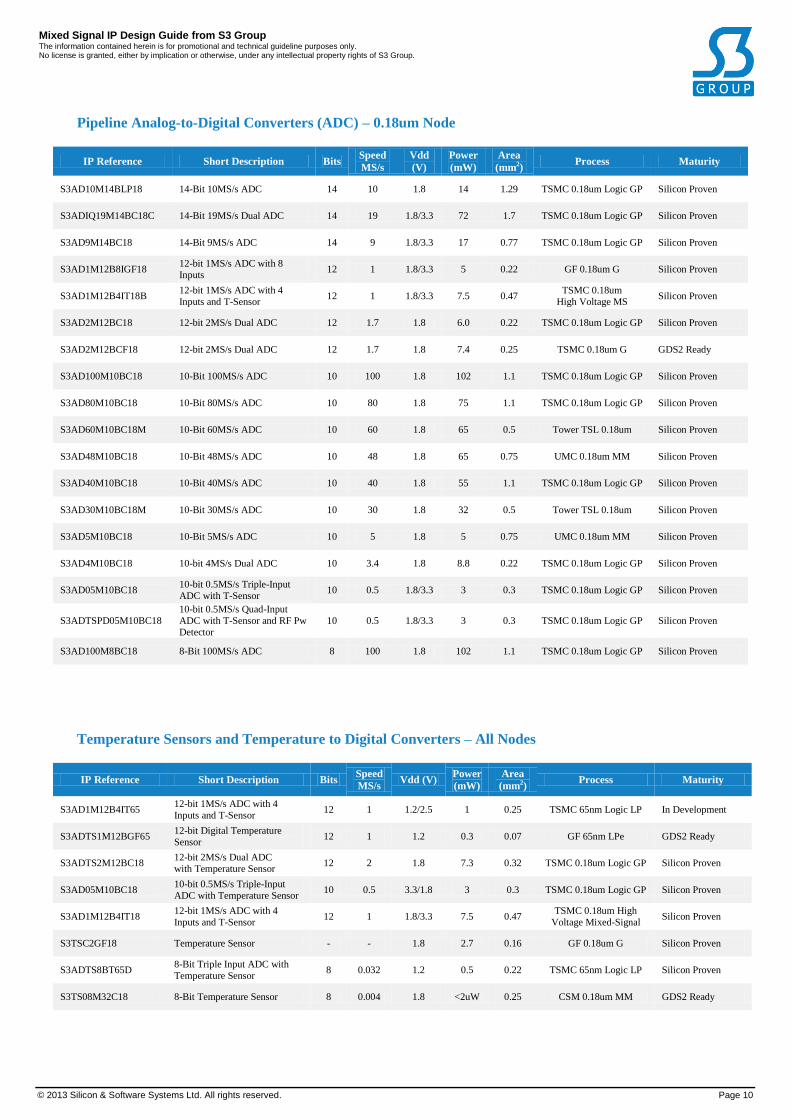
Pipeline Analog-to-Digital Converters (ADC) – 0.18um Node
IP Reference Short Description Bits Speed
MS/s
Vdd
(V)
Power
(mW)
Area
(mm2) Process Maturity
S3AD10M14BLP18 14-Bit 10MS/s ADC 14 10 1.8 14 1.29 TSMC 0.18um Logic GP Silicon Proven
S3ADIQ19M14BC18C 14-Bit 19MS/s Dual ADC 14 19 1.8/3.3 72 1.7 TSMC 0.18um Logic GP Silicon Proven
S3AD9M14BC18 14-Bit 9MS/s ADC 14 9 1.8/3.3 17 0.77 TSMC 0.18um Logic GP Silicon Proven
S3AD1M12B8IGF18 12-bit 1MS/s ADC with 8
Inputs 12 1 1.8/3.3 5 0.22 GF 0.18um G Silicon Proven
S3AD1M12B4IT18B 12-bit 1MS/s ADC with 4
Inputs and T-Sensor 12 1 1.8/3.3 7.5 0.47
TSMC 0.18um
High Voltage MS Silicon Proven
S3AD2M12BC18 12-bit 2MS/s Dual ADC 12 1.7 1.8 6.0 0.22 TSMC 0.18um Logic GP Silicon Proven
S3AD2M12BCF18 12-bit 2MS/s Dual ADC 12 1.7 1.8 7.4 0.25 TSMC 0.18um G GDS2 Ready
S3AD100M10BC18 10-Bit 100MS/s ADC 10 100 1.8 102 1.1 TSMC 0.18um Logic GP Silicon Proven
S3AD80M10BC18 10-Bit 80MS/s ADC 10 80 1.8 75 1.1 TSMC 0.18um Logic GP Silicon Proven
S3AD60M10BC18M 10-Bit 60MS/s ADC 10 60 1.8 65 0.5 Tower TSL 0.18um Silicon Proven
S3AD48M10BC18 10-Bit 48MS/s ADC 10 48 1.8 65 0.75 UMC 0.18um MM Silicon Proven
S3AD40M10BC18 10-Bit 40MS/s ADC 10 40 1.8 55 1.1 TSMC 0.18um Logic GP Silicon Proven
S3AD30M10BC18M 10-Bit 30MS/s ADC 10 30 1.8 32 0.5 Tower TSL 0.18um Silicon Proven
S3AD5M10BC18 10-Bit 5MS/s ADC 10 5 1.8 5 0.75 UMC 0.18um MM Silicon Proven
S3AD4M10BC18 10-bit 4MS/s Dual ADC 10 3.4 1.8 8.8 0.22 TSMC 0.18um Logic GP Silicon Proven
S3AD05M10BC18 10-bit 0.5MS/s Triple-Input
ADC with T-Sensor 10 0.5 1.8/3.3 3 0.3 TSMC 0.18um Logic GP Silicon Proven
S3ADTSPD05M10BC18
10-bit 0.5MS/s Quad-Input
ADC with T-Sensor and RF Pw
Detector
10 0.5 1.8/3.3 3 0.3 TSMC 0.18um Logic GP Silicon Proven
S3AD100M8BC18 8-Bit 100MS/s ADC 8 100 1.8 102 1.1 TSMC 0.18um Logic GP Silicon Proven
Temperature Sensors and Temperature to Digital Converters – All Nodes
IP Reference Short Description Bits Speed
MS/s Vdd (V)
Power
(mW)
Area
(mm2) Process Maturity
S3AD1M12B4IT65 12-bit 1MS/s ADC with 4
Inputs and T-Sensor 12 1 1.2/2.5 1 0.25 TSMC 65nm Logic LP In Development
S3ADTS1M12BGF65 12-bit Digital Temperature
Sensor 12 1 1.2 0.3 0.07 GF 65nm LPe GDS2 Ready
S3ADTS2M12BC18 12-bit 2MS/s Dual ADC
with Temperature Sensor 12 2 1.8 7.3 0.32 TSMC 0.18um Logic GP Silicon Proven
S3AD05M10BC18 10-bit 0.5MS/s Triple-Input
ADC with Temperature Sensor 10 0.5 3.3/1.8 3 0.3 TSMC 0.18um Logic GP Silicon Proven
S3AD1M12B4IT18 12-bit 1MS/s ADC with 4
Inputs and T-Sensor 12 1 1.8/3.3 7.5 0.47
TSMC 0.18um High
Voltage Mixed-Signal Silicon Proven
S3TSC2GF18 Temperature Sensor - - 1.8 2.7 0.16 GF 0.18um G Silicon Proven
S3ADTS8BT65D 8-Bit Triple Input ADC with
Temperature Sensor 8 0.032 1.2 0.5 0.22 TSMC 65nm Logic LP Silicon Proven
S3TS08M32C18 8-Bit Temperature Sensor 8 0.004 1.8 <2uW 0.25 CSM 0.18um MM GDS2 Ready

Mixed Signal IP Design Guide from S3 Group The information contained herein is for promotional and technical guideline purposes only. No license is granted, either by implication or otherwise, under any intellectual property rights of S3 Group.
© 2013 Silicon & Software Systems Ltd. All rights reserved. Page 11
Digital-to-Analog Converters (DAC) – 40m Node
IP Reference Short Description Bits Speed
MS/s
Vdd
(V)
Power
(mW)
Area
(mm2) Process Maturity
S3DA250M12BT40 12-Bit 250MS/s DAC 12 250 1.1/2.5 17 0.23 TSMC 40nm Logic LP In Development
S3DAIQ80M12BT40 12-Bit 80MS/s Dual DAC 12 80 1.1/2.5 16 0.2 TSMC 40nm Logic LP GDS2 Ready
S3DAIQ62M12BT40LPA 12-Bit 62MS/s Dual DAC 12 62 1.1/2.5 16 0.2 TSMC 40nm Logic LP Silicon Proven
S3DA5M11BT40LPA 11-Bit 5MS/s Voltage DAC 11 5 1.1/2.5 5 0.1 TSMC 40nm Logic LP Silicon Proven
S3TD200M10BT40G18A 10-Bit 200MS/s Triple Voltage
DAC 10 200 0.9/1.8 0.12A 0.7 TSMC 40nm G Silicon Proven
Digital-to-Analog Converters (DAC) – 65m & 55nm Nodes
IP Reference Short Description Bits Speed
MS/s
Vdd
(V)
Power
(mW)
Area
(mm2) Process Maturity
S3DA300M14B65 14-Bit 300MS/s DAC 14 300 1.2/2.5 70 0.8 TSMC 65nm Logic LP In Development
S3DA300M12BT65D 12-Bit 300MS/s DAC 12 300 1.2/2.5 17 0.23 TSMC 65nm Logic LP Silicon Proven
S3DA300M12BCH65LPEA 12-Bit 300MS/s DAC 12 300 1.2/3.3 23 0.26 CSM 65nm LPe Silicon Proven
S3DA300M12BC55LPA 12-Bit 300MS/s DAC 12 300 1.2/3.3 23 0.22 UMC 55nm LP Silicon Proven
S3TD300M12BT65GPA 12-Bit 300MS/s Triple DAC 12 300 1.0/2.5 285 0.5 TSMC 65nm Logic GP Silicon Proven
S3TD300M12BT55GPA 12-Bit 300MS/s Triple DAC 12 300 1.0/2.5 285 0.5 TSMC 55nm Logic GP Silicon Proven
S3DA231M12BT65D 12-Bit 231MS/s DAC 12 231 1.2/2.5 23 0.23 TSMC 65nm Logic LP Silicon Proven
S3DADDS212M12BT65LPH 12-Bit 212MS/s DDS DAC 12 212 1.2/2.5 60 0.2 TSMC 65nm Logic LP Silicon Proven
S3DAIQ212M12BT65LPH 12-Bit 212MS/s Dual DAC 12 212 1.2/2.5 123 0.4 TSMC 65nm Logic LP Silicon Proven
S3DA200M12BCH65G 12-Bit 200MS/s DAC 12 200 1.0/3.3 20 0.15 CSM 65nm G Silicon Proven
S3DAIQ160M12BT65 12-Bit 160MS/s Dual DAC 12 160 1.2/2.5 35 0.31 TSMC 65nm Logic LP Silicon Proven
S3TD160M12B65G 12-Bit 160MS/s Triple DAC 12 160 1.0/2.5 290 0.4 TSMC 65nm Logic GP In Development
S3DAIQ125M12BT65 12-Bit 125MS/s Dual DAC 12 125 1.2/2.5 30 0.4 TSMC 65nm Logic LP GDS2 Ready
S3DAIQ125M12BGF65LPE 12-Bit 125MS/s Dual DAC 12 125 1.2/2.5 30 0.4 GF 65nm LPe Silicon Proven
S3DAIQ80M12BT65 12-Bit 80MS/s Dual DAC 12 80 1.2/2.5 30 0.31 TSMC 65nm Logic LP Silicon Proven
S3DA40M12BT65LPA 12-Bit 40MS/s DAC 12 40 1.2/3.3 126 0.2 TSMC 65nm Logic LP Silicon Proven
S3QD300M10BT55LPA3 10-Bit 300MS/s Quad DAC 10 300 1.2/3.3 307 0.42 TSMC 55nm Logic LP GDS2 Ready
S3TD240M10BT65LPA 10-Bit 240MS/s Triple DAC 10 240 1.2/2.5 285 0.38 TSMC 65nm Logic LP Silicon Proven
S3QD240M10BT65GPA 10-Bit 240MS/s Quad DAC 10 240 1.0/2.5 375 0.52 TSMC 65nm Logic GP GDS2 Ready
S3TD240M10BT65GP3A 10-Bit 240MS/s Triple DAC 10 240 1.0/3.3 370 0.4 TSMC 65nm Logic GP In Development
S3TD240M10BT65GPA 10-Bit 240MS/s Triple DAC 10 240 1.0/2.5 285 0.4 TSMC 65nm Logic GP In Development
S3DA200M10BCH65G 10-Bit 200MS/s DAC 10 200 1.0/3.3 20 0.15 CSM 65nm G Silicon Proven
S3TD162M10BT55GP3A 10-Bit 162MS/s Triple DAC 10 162 1.0/3.3 230 0.4 TSMC 55nm Logic GP Silicon Proven
S3DAIQ160M10BT65 10-Bit 160MS/s Dual DAC 10 160 1.2/2.5 35 0.31 TSMC 65nm Logic LP Silicon Proven
S3DA100K10BT65LPH 10-Bit 100kS/s Voltage DAC 10 0.1 1.2/2.5 1.0 0.125 TSMC 65nm Logic LP Silicon Proven

Mixed Signal IP Design Guide from S3 Group The information contained herein is for promotional and technical guideline purposes only. No license is granted, either by implication or otherwise, under any intellectual property rights of S3 Group.
© 2013 Silicon & Software Systems Ltd. All rights reserved. Page 12
Digital-to-Analog Converters (DAC) – 90nm Node
IP Reference Short Description Bits Speed
MS/s
Vdd
(V)
Power
(mW)
Area
(mm2) Process Maturity
S3DA300M12B90G3B 12-Bit 300MS/s DAC 12 300 1.0/3.3 124 0.16 TSMC 90nm Logic GP Silicon Proven
S3TD160M12B90G3 12-Bit 160MS/s Triple DAC 12 160 1.0/3.3 306 0.5 TSMC 90nm Logic GP Silicon Proven
S3DA80M12BC90 12-Bit 80MS/s DAC 12 80 1.2/2.5 17.5 0.18 TSMC 90nm Logic LP Silicon Proven
S3DAIQ80M12BC90 12-Bit 80MS/s Dual DAC 12 80 1.2/3.3 37 0.29 TSMC 90nm Logic LP Silicon Proven
S3DA160M10BC90 10-Bit 160MS/s DAC 10 160 1.2 16 0.23 TSMC 90nm Logic LP Silicon Proven
S3DAIQ160M10BC90 10-Bit 160MS/s Dual DAC 10 160 1.2 30 0.4 TSMC 90nm Logic LP Silicon Proven
S3DA2M10BT90LPA 10-Bit Voltage DAC 10 2 1.2/3.3 30 0.2 TSMC 90nm Logic LP Silicon Proven
S3DACMPTD8C90
8-bit 10MS/s 8-Channels DAC
with Programmable
Comparators
8 10 1.2/3.3 8 0.5 TSMC 90nm Logic GP Silicon Proven
S3DA1M8BC90 8-Bit 1MS/s DAC 8 1 1.2/3.3 10 0.1 TSMC 90nm Logic LP Silicon Proven
Digital-to-Analog Converters (DAC) – 0.13um Node
IP Reference Short Description Bits Speed
MS/s
Vdd
(V)
Power
(mW)
Area
(mm2) Process Maturity
S3DA300M10BC13 10-Bit 300MS/s DAC 10 300 1.2/3.3 21.5 0.15 UMC 130nm Logic HS Silicon Proven
S3DA160M10B1V2C13 10-Bit 160MS/s DAC 10 160 1.2 4 0.15 UMC 130nm Logic HS Silicon Proven
S3DA160M10BC13 10-Bit 160MS/s DAC 10 160 1.2/3.3 76 0.2 UMC 130nm Logic HS Silicon Proven
S3DA160M10BC13B 10-Bit 160MS/s DAC 10 160 1.2 33 0.22 UMC 130nm Logic HS Silicon Proven
S3DAIQ160M10BC13B 10-Bit 160MS/s Dual DAC 10 160 1.2 62 0.55 UMC 130nm Logic HS Silicon Proven
S3DA80M10BC13 10-Bit 80MS/s DAC 10 80 1.2/3.3 17.5 0.2 UMC 130nm Logic HS Silicon Proven
Digital-to-Analog Converters (DAC) – 0.18um Node
IP Reference Short Description Bits Speed
MS/s
Vdd
(V)
Power
(mW)
Area
(mm2) Process Maturity
S3DA400M12BC18 12-Bit 400MS/s DAC 12 400 1.8/3.3 79 0.6 TSMC 0.18um Logic GP Silicon Proven
S3DA300M12BC18 12-Bit 300MS/s DAC 12 300 1.8/3.3 90 0.8 TSMC 0.18um Logic GP Silicon Proven
S3DAIQ20M12BC18 12-bit 20MS/s Dual DAC 12 20 1.8/3.3 37 0.77 TSMC 0.18um Logic GP Silicon Proven
S3DA20M12BC18A 12-bit 20MS/s DAC 12 20 1.8/3.3 90 0.68 TSMC 0.18um Logic GP Silicon Proven
S3DA400M10BC18 10-Bit 400MS/s DAC 10 400 1.8/3.3 80 0.8 TSMC 0.18um Logic GP Silicon Proven
S3DA160M10BC18 10-Bit 160MS/s DAC 10 160 1.8/3.3 29.5 0.8 TSMC 0.18um Logic GP Silicon Proven
S3DA100K10BC18 10-Bit 100kS/s Voltage DAC 10 0.1 3.3 1 0.15 TSMC 0.18um RF
CMOS Silicon Proven
S3DA100K10BC18A 10-bit 100kS/s DAC 10 0.1 1.8/3.3 1 0.16 TSMC 0.18um Logic GP Silicon Proven
S3DA250M8BC18 8-Bit 250MS/s DAC 8 250 1.8/3.3 5.3 0.08 TSMC 0.18um Logic GP Silicon Proven

Mixed Signal IP Design Guide from S3 Group The information contained herein is for promotional and technical guideline purposes only. No license is granted, either by implication or otherwise, under any intellectual property rights of S3 Group.
© 2013 Silicon & Software Systems Ltd. All rights reserved. Page 13
Phase-Locked Loops (PLL) – All Nodes
IP Reference Short Description Features (MHz) Vdd
(V)
Power
(mW)
Area
(mm2) Process Maturity
S3PLLT40LPA Low Noise Programmable PLL Vco=600-1250, Out=5 to 600 1.1/2.5 11 0.28 TSMC 40nm Logic LP Silicon Proven
S3PLLT40LP Low Noise Programmable PLL Vco=600-1300, Out=4 to 600 1.1/2.5 9 0.18 TSMC 40nm Logic LP GDS2 Ready
S3ULJPLLT65A Ultra-Low Jitter PLL for High
Performance ADC Applications
Vco=1,650-1,850
Long-term Jitter < 1ps-rms 1.2/2.5 50 0.4
TSMC 65nm Logic LP
+ UTM option In Development
S3ULJPLLT65B
Ultra-Low Jitter PLLw/
Integrated Loop Filter for High
Performance ADC Applications
Output Frequency 1.6 to
1.8GHz or Lower
Long-term Jitter < 0.5ps-rms
1.2 55 0.5 TSMC 65nm Logic LP In Development
S3PLLT65A Low Noise Programmable PLL Vco=600-1,200,
Out=9.5 -1200 1.2 8 0.25 TSMC 65nm Logic LP Silicon Proven
S3PLLT65D Low Noise Programmable PLL Vco=600-1200,
Out=9.5 to 600 1.2 9 0.28 TSMC 65nm Logic LP Silicon Proven
S3PLLFDGF65LPE Low Noise Fractional PLL Vco=240-320,
Out=1-80, 120-160 1.2 2 0.05 GF 65nm Logic LPe GDS2 Ready
S3PLLT65F Low Noise Programmable PLL Vco=600-1200, Out=9.5-1200 1.2 8 0.25 TSMC 65nm Logic LP Silicon Proven
S3PLLCH65LPEB Low Noise Programmable PLL Vco=900-1080,
Out=243, 256, 270 1.2/3.3 13 0.24 CSM 65nm LPe Silicon Proven
S3PLLCH65G Low Noise Programmable PLL Vco = 900-1,000, Out1=60 to
900, Out2=66.7 to 1000 1.0/3.3 12 0.2 CSM 65nm G Silicon Proven
S3PLLT65LPH Low Noise Programmable PLL Vco=600-1200,
Out=9.5 to 600 1.2 7 0.28 TSMC 65nm Logic LP Silicon Proven
S3PLLFRACT65 Low Noise Fractional PLL Vco=600-1200,
Out=9.5 to 600 1.2 10 0.3 TSMC 65nm Logic LP GDS2 Ready
S3PLLSM65LPA Low Noise Programmable PLL Vco=600-1200,
Out=4.72 to 600 1.2 5.2 0.28 SMIC 65nm LL Silicon Proven
S3PLLCH65LPEA Low Noise Programmable PLL Vco=900-1000, Out=60-1000 1.2/3.3 12 0.24 CSM 65nm LPe Silicon Proven
S3PLLCH65LPA Low Noise Programmable PLL Vco=900-1000, Out=125-1000 1.2/3.3 12 0.2 CSM 65nm LPe GDS2 Ready
S3PLLC55LPA Low Noise Programmable PLL Vco=900-1000, Out=60-1000 1.2/3.3 12 0.24 UMC 55nm LP Silicon Proven
S3PLLT90GA Low Noise Programmable PLL Vco=750, Fout=250 to 375 1.2 6 0.22 TSMC 90nm Logic GP Silicon Proven
S3PLL250LN90LP Low Noise Programmable PLL Vco=480-960,
Out=3.75 to 960 1.2 3 0.2 TSMC 90nm Logic LP Silicon Proven
S3PLLPROGC90 Low Noise Programmable PLL Vco=700-1200,
Out=11.1 to 1200 1.2 4 0.2 TSMC 90nm Logic LP Silicon Proven
S3PLLSM90LP Low Noise Programmable PLL Vco=480-960,
Out=3.75 to 960 1.2 3 0.2 SMIC 90nm LP Silicon Proven
S3PLLPROGC13 Low Noise Programmable PLL Vco=300, Out=4.8 to 1,200 1.2 2.5 0.16 UMC 130nm Logic HS Silicon Proven
S3PLLPROGC18 Low Noise Programmable PLL Vco=250-550, Out=30 to 550 1.8 4 0.1 TSMC 0.18um Logic GP Silicon Proven
S3ULJPLLC18 Ultra-Low Jitter PLL for High
Performance ADC Applications
VCO Frequency 1.6 to 1.8GHz
Output Frequency 5 to
300MHz
Long-term Jitter < 1.2ps-rms
1.8/3.3 56 0.75 TSMC 0.18um RF CMOS Silicon Proven
S348MPLLC18 Low Noise Programmable PLL Vco=480, Out=48 1.8 8.8 0.42 UMC 0.18um MM Silicon Proven

Mixed Signal IP Design Guide from S3 Group The information contained herein is for promotional and technical guideline purposes only. No license is granted, either by implication or otherwise, under any intellectual property rights of S3 Group.
© 2013 Silicon & Software Systems Ltd. All rights reserved. Page 14
Power Management Platform
IP Reference Short Description Features Process Maturity
S3PMPGF18 Customizable Power
Management Platform
Contains DC-DC Converters, LDOs, POR, RTC,
OSC, Aux ADC, T-Sensor etc. GF 0.18um Silicon Proven
Power Management: DC-DC Converters – All Nodes
IP Reference Short Description Features Area
(mm2) Process Maturity
S3DC521TC18LP DC-DC Converter 100mA load, 2.7 to 5.5V in, 1.8V out 0.75 SSMC 0.18um Silicon Proven
S3DCC51XGF18 DC-DC Controller
5V and 1.8V supplies, 0.68 - 3.6V out, 100mA to 8A load,
Integrated compensation and adjustable
switching frequency
0.71 GF 0.18um IC Silicon Proven
S3DCC31XT28 DC-DC Controller
Power Supply from 1.71V to 3.46V, 0.81 to 1.2V, 100mA to 3A load,
Programmable Output Voltage,
Adjustable switching frequency
0.56 TSMC 28nm HPL Silicon Proven
Power Management: Miscellaneous – All Nodes
IP Reference Short Description Features Area
(mm2) Process Maturity
S3PORT28L Power On Reset Circuit 1.8V, 1.8-3.3V, 0.9-1.0V Sense Supplies 0.085 TSMC 28nm HPL Silicon Proven
S3PORTC18B Power On Reset Circuit 3.3V, 3.3V and 1.8V Sense Supplies 0.053 TSMC 0.18um G GDS2 Ready
S3DVDT55LP3 Dual Supply Voltage Detector I/O 3.3V and Core Supply 1.2V 0.03 TSMC 55nm Logic LP GDS2 Ready
S3PORSM65LPA Power On Reset Circuit 1.2V 0.04 SMIC 65nm LL Silicon Proven
S3PMSM65LPA Power Switch Circuit 1.2V 0.01 SMIC 65nm LL Silicon Proven
S3PMT90LP Power Switch 1.2V 0.008 TSMC 90nm Logic LP Silicon Proven
S3PORC90LP Power On Reset 1.2V, 0.02mW 0.04 TSMC 90nm Logic LP Silicon Proven
S3PORTC90 Power On Reset Circuit with
RC-Oscillator output 3.3V, 0.9mW 0.05 TSMC 90nm Logic LP Silicon Proven
S3PORSM90LP Power On Reset 1.2V, 0.02mW 0.04 SMIC 90nm LL Silicon Proven
S3PMSM90LP Power Switch for Voltage
Islands 0.5 Ohm, 20mA SMIC 90nm LL Silicon Proven
S3PORTC18D Power On Reset Circuit 130uA
3.3V & 1.8V Sense Supplies 0.05
TSMC 0.18um High
Voltage Mixed-Signal Silicon Proven
S3CSAIINT18M Current-Sense Voltage
Amplifier, Low Bandwidth 6.2mW TSMC 0.18um Logic GP Silicon Proven
S3CSAILT18M Current-Sense Voltage
Amplifier, High Bandwidth 6.5mW TSMC 0.18um Logic GP Silicon Proven
S3VBUFT18M Voltage Buffer 10mW TSMC 0.18um Logic GP Silicon Proven
S3PORT18 Power On Reset 3.3V and 1.8V Sense Supplies 0.05 TSMC 0.18um Logic GP Silicon Proven
S3PORTC18BI Power On Reset w/ Brown-Out
Detection
Power: 0.3mW
3.3V, 1.8V & 1.2V Sense Supplies
3.3/1.8/
1.2 TSMC 0.18um Logic GP Silicon Proven
S3PORTC18B Power On Reset 3.3V and 1.8V Sense Supplies 0.05 TSMC 0.18um Logic GP Silicon Proven
S3OSC30MGF18 32MHz RC Oscillator 1.8V, 32MHz output, 400uA 0.2 GF 0.18um IC Silicon Proven

Mixed Signal IP Design Guide from S3 Group The information contained herein is for promotional and technical guideline purposes only. No license is granted, either by implication or otherwise, under any intellectual property rights of S3 Group.
© 2013 Silicon & Software Systems Ltd. All rights reserved. Page 15
Power Management: LDOs – All Nodes
IP Reference Short Description Features Area
(mm2) Process Maturity
S3REG00316GF65LPE LDO Regulator 3mA load, 1.6-3.6V in, 1.15-1.26V out 0.01 GF 65nm Logic LPe GDS2 Ready
S3REG00116GF65LPE LDO Regulator 1mA load, 1.6-3.6V in, 1.15-1.26V out 0.008 GF 65nm Logic LPe GDS2 Ready
S3REG10016T65LD LDO Regulator 100mA load, 1.6-3.6V in, 1.2-3.0V out 0.08 TSMC 65nm Logic LP GDS2 Ready
S3REG1016T65LD LDO Regulator 10mA load, 1.6-2.0V in, 1.2V out 0.045 TSMC 65nm Logic LP GDS2 Ready
S3REG25016T65LD LDO Regulator 250mA load, 1.6-2.0V in, 1.2V out 0.14 TSMC 65nm Logic LP GDS2 Ready
S3REGC10014T65LD LDO Regulator, Capless 100mA load, 1.4-3.3V in, 1.1-3.0V out 0.11 TSMC 65nm Logic LP GDS2 Ready
S3REGT65A LDO Regulator 150mA load, 1.45-2.5V in, 1.3V out 0.72 TSMC 65nm Logic LP Silicon Proven
S3REG15014T65L LDO Regulator 150mA load, 1.4-3.6V in, 1.1-3.0V out 0.19 TSMC 65nm Logic LP GDS2 Ready
S3REG8014T65L LDO Regulator 80mA load, 1.4-3.6V in, 1.0-1.3V out 0.15 TSMC 65nm Logic LP Silicon Proven
S3REGC5014T65L LDO Regulator, Capless 50mA load, 1.4-3.3V in, 1.1-3.0V out 0.1 TSMC 65nm Logic LP GDS2 Ready
S3REG15018T65L LDO Regulator 150mA load, 1.8-3.6V in, 1.1-3.0V out 0.11 TSMC 65nm Logic LP In Development
S3REG25016T65L LDO Regulator 250mA load, 1.6-2V in, 1.2V out 0.13 TSMC 65nm Logic LP Silicon Proven
S3REG10016T65L LDO Regulator 100mA load, 1.6-3.6V in, 1.2-3.0V out 0.08 TSMC 65nm Logic LP Silicon Proven
S3REG1016T65L LDO Regulator 10mA load, 1.6-2V in, 1.2V out 0.05 TSMC 65nm Logic LP Silicon Proven
S3REG20025T90 LDO Regulator 200mA load, 2.5-3.6V in, 1.2V out 0.12 TSMC 90nm Logic LP Silicon Proven
S3REG104HVT18 LDO Regulator 10mA load, 4-15V in, 3.3V out 0.2 TSMC 0.18um
High Voltage MS Silicon Proven
S3REG5033TC18 LDO Regulator 50mA load, 3.3V in, 1.8V out 0.2 TSMC 0.18um
High Voltage MS Silicon Proven
S3REG605GF18 LDO Regulator 100mA load, 2.7-5.5V in, 1.8V out 0.23 GF 0.18um IC Silicon Proven
S3REGU155GF18 LDO Regulator 15uA load, 2.5-3.6V in, 1.8V out 0.18 GF 0.18um IC Silicon Proven
S3REGSS60015GF18 LDO Regulator 400mA load, 1.5V in, 0.625-0.99V out
600mA load, 1.5V in, 0.98V-1.28V out 0.95 GF 0.18um IC Silicon Proven
S3REG115GF18 LDO Regulator 1mA load, 1.5V in, 0.625 – 0.99V out 0.04 GF 0.18um IC Silicon Proven
S3REG2052V5T18 LDO Regulator 20mA load, 3.15 to 5V Vin, 2.5V out 0.124 TSMC 0.18um Logic GP Silicon Proven
S3REG8051V8T18 LDO Regulator 80mA load, 3.15 to 5V Vin, 1.8V out 0.135 TSMC 0.18um Logic GP Silicon Proven
S3REG8053V0T18 LDO Regulator 80mA load, 3.15 to 5V Vin, 3.1V out 0.2 TSMC 0.18um Logic GP Silicon Proven
S3REG20033TC18M LDO Regulator 200mA load, 2.6 to 3.6V Vin, 1.8V out 0.07 TSMC 0.18um Logic GP Silicon Proven
S3REG10030TC18A LDO Regulator 100mA load. 3.0 to 3.6V in. 1.8V out.
>64dB PSRR 0.1
TSMC 0.18um RF
CMOS Silicon Proven
S3REG2030TC18 LDO Regulator 20mA load. 3.0 to 3.6V in. 1.8V out 0.06 TSMC 0.18um RF
CMOS Silicon Proven
S3REG2031TC18A LDO Regulator
20mA load. 3.15 to 3.45V in.
2.5-2.7V out.
>72dB PSRR
0.12 TSMC 0.18um RF
CMOS Silicon Proven

Mixed Signal IP Design Guide from S3 Group The information contained herein is for promotional and technical guideline purposes only. No license is granted, either by implication or otherwise, under any intellectual property rights of S3 Group.
© 2013 Silicon & Software Systems Ltd. All rights reserved. Page 16
: www.s3group.com/consumer-silicon/mixed-signal-ip/
Standard IP Deliverables Datasheet
Characterization Report
Flat Netlist (cdl)
Layout View (gds2)
Abstract View (lef)
Timing View (tlf)
Behavioral Model (VHDL/Verilog)
Integration Support
Mixed Signal Design At S3 Group
S3 Group has been delivering mixed signal design solutions for more than 15 years. We have a proven track record in the
efficient delivery of complex mixed signal designs. Our success is based on multiple design disciplines in areas such as RF,
Analog, DSP and Digital Design combined with in-depth application knowledge and project management expertise. Our mixed signal design capability includes a number of important elements:
A library of customizable IP components
Extensive experience of Deep Sub Micron mixed-signal design and IP integration
Focused experts in key circuit technologies
Standardized design methodologies
Systems design knowledge
Silicon evaluation capability
Project management expertise
ISO 9001 Quality certification
About S3 Group
S3 Group delivers IP and professional services to OEMs, system vendors and semiconductor companies. The company is the longest
serving independent service provider in the industry, building a wealth of experience and engineering expertise over the last 25 years.
In addition to design services the company has a comprehensive portfolio of RF and Mixed-Signal IP. The IP portfolio includes high
performance ADC and DAC converters, PLLs, Analog Front Ends (AFEs), Power Management, RF Transceivers and other
miscellaneous circuits which have been silicon proven at a number of silicon foundries (TSMC, GlobalFoundries, UMC, SMIC, IBM,
Tower) at nodes ranging from 180nm to 40nm and below. Global end markets served by S3 Group clients include Wireless and
Wireline Communications, Digital Broadcasting, Imaging, Solar, Green Energy and Industrial. Founded in 1986, S3 Group,
headquartered in Dublin, Ireland, focuses on three business areas: Semiconductor, TV Technology and Telehealth, and has
development centers in Ireland, Poland, the Czech Republic and Portugal with sales offices and representatives worldwide.
For further information
E-mail: [email protected]
Website: www.s3group.com/silicon