Embed Size (px)
Citation preview

SPECIFICATION V2.0
TS04
4-Channel Self Calibration Capacitive Touch Sensor

TS04 (4-CH Auto Sensitivity Calibration Capacitive Touch Sensor)
1
1 Specification
1.1 General Feature
4-Channel capacitive sensor with auto sensitivity calibration
Parallel output interface
Independently adjustable sensitivity with external capacitor
Adjustable internal frequency with external resister
Embedded high frequency noise elimination circuit
Low current consumption
RoHS compliant 16QFN, 14SOP package
1.2 Application
Mobile application (mobile phone / PDA / PMP / MP3 etc)
Membrane switch replacement
Sealed control panels, keypads
Door key-lock matrix application
1.3 Package (16 QFN / 14SOP)
16 QFN 14SOP
Drawings not to scale

TS04 (4-CH Auto Sensitivity Calibration Capacitive Touch Sensor)
2
2 Pin Description
2.1 16 QFN package
PIN No. Name I/O Description Protection
1 N.C. - Not connect -
2 RBIAS Analog Input Internal bias adjust input VDD/GND
3 GND - Connect to GND VDD/GND
4 CS1 Analog Input CH1 capacitive sensor input VDD/GND
5 CS2 Analog Input CH2 capacitive sensor input VDD/GND
6 CS3 Analog Input CH3 capacitive sensor input VDD/GND
7 Dummy Analog Input Internal noise monitoring input
Do not connect to anywhere VDD/GND
8 GND Ground Supply ground VDD
9 CS4 Analog Input CH4 capacitive sensor input VDD/GND
10 OUT1 Digital Output Output1 for CS1 (Open Drain structure) VDD/GND
11 OUT2 Digital Output Output2 for CS2 (Open Drain structure) VDD/GND
12 GND Ground Supply ground VDD
13 OUT3 Digital Output Output3 for CS3 (Open Drain structure) VDD/GND
14 OUT4 Digital Output Output4 for CS4 (Open Drain structure) VDD/GND
15 GND - Connect to GND VDD/GND
16 VDD Power Power (2.5V~5.0V) GND

TS04 (4-CH Auto Sensitivity Calibration Capacitive Touch Sensor)
3
2.2 14 SOP
PIN No. Name I/O Description Protection
1 GND - Connect to GND VDD/GND
2 VDD Power Power (2.5V~5.0V) GND
3 RBIAS Analog Input Internal bias adjust input VDD/GND
4 CS1 Analog Input CH1 capacitive sensor input VDD/GND
5 CS2 Analog Input CH2 capacitive sensor input VDD/GND
6 CS3 Analog Input CH3 capacitive sensor input VDD/GND
7 Dummy Analog Input Internal noise monitoring input
Do not connect to anywhere VDD/GND
8 GND Ground Supply ground VDD
9 CS4 Analog Input CH4 capacitive sensor input VDD/GND
10 OUT1 Digital Output Output1 for CS1 (Open Drain structure) VDD/GND
11 OUT2 Digital Output Output2 for CS2 (Open Drain structure) VDD/GND
12 GND Ground Supply ground VDD
13 OUT3 Digital Output Output3 for CS3 (Open Drain structure) VDD/GND
14 OUT4 Digital Output Output4 for CS4 (Open Drain structure) VDD/GND
TS04 (4-CH Auto Sensitivity Calibration Capacitive Touch Sensor)
4
3 Absolute Maximum Rating Battery supply voltage 5.0V
Maximum voltage on any pin VDD+0.3
Maximum current on any PAD 100mA
Power Dissipation 800mW
Storage Temperature -50 ~ 150
Operating Temperature -20 ~ 75
Junction Temperature 150
Note Unless any other command is noted, all above are operated in normal temperature.
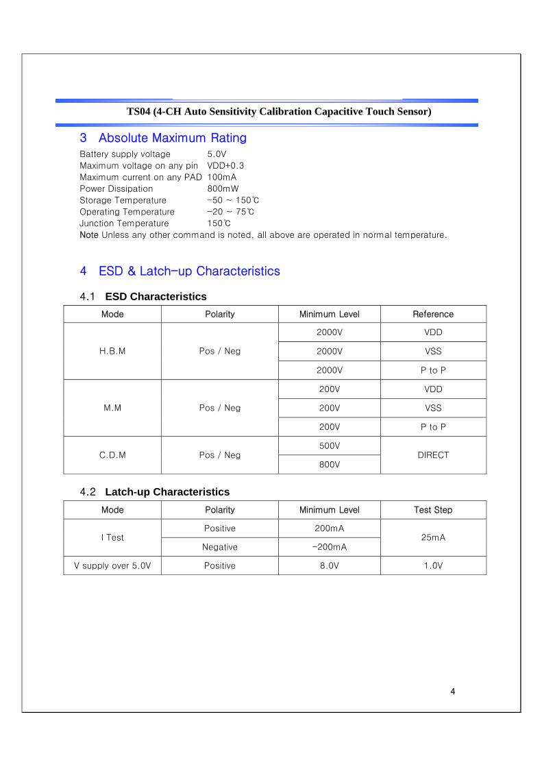
4 ESD & Latch-up Characteristics
4.1 ESD Characteristics Mode Polarity Minimum Level Reference
2000V VDD
2000V VSS H.B.M Pos / Neg
2000V P to P
200V VDD
200V VSS M.M Pos / Neg
200V P to P
500V C.D.M Pos / Neg
800V DIRECT
4.2 Latch-up Characteristics Mode Polarity Minimum Level Test Step
Positive 200mA I Test
Negative -200mA 25mA
V supply over 5.0V Positive 8.0V 1.0V

TS04 (4-CH Auto Sensitivity Calibration Capacitive Touch Sensor)
5
5 Electrical Characteristics
VDD=3.3V, Rb=510k, Sync Mode (Rsync = 2MΩ) (Unless otherwise noted), TA = 25
Characteristics Symbol Test Condition Min Typ Max Units
Operating supply
voltage VDD 2.5 3.3 5.0 V
VDD= 3.3V RB=510k RSB=0 - 40 70 Current consumption IDD
VDD= 5.0V RB=510k RSB =0 - 80 140
Digital output
maximum sink currentIOUT TA = 25 (Normal I2C Output) - - 4.0
Internal reset criterion
VDD voltage VDD_RST TA = 25, RB=510k - - 0.3∙VDD V
Sense input
capacitance range
[Note1]
CS - - 100
Minimum detective
capacitance differenceΔC
Cs = 10pF
0.2 - -
ΔC > 0.2pF, Cs = 10pF - 12 - Output impedance
(open drain) ZO
ΔC < 0.2pF, Cs = 10pF - 30M - Ω
VDD = 3.3V RB = 510k - 100 - Self calibration time
after system reset TCAL
VDD = 5.0V RB = 510k - 80 - ms
Sense input
resistance range RS - 200 1000 Ω
VDD = 3.3V 200 510 820 Recommended bias
resistance range
[Note2]
RB VDD = 5.0V 330 620 1200
kΩ
Maximum bias
capacitance CB_MAX - 820 1000 pF
Note 1 : The sensitivity can be increased with lower CS value.
The recommended value of CS is 10pF when using 3T PC(Poly Carbonate) cover and
10 x 7 touch pattern.
Note 2 : The lower RB is recommended in noisy condition.
TS04 (4-CH Auto Sensitivity Calibration Capacitive Touch Sensor)
6
6 Implementation of TS04
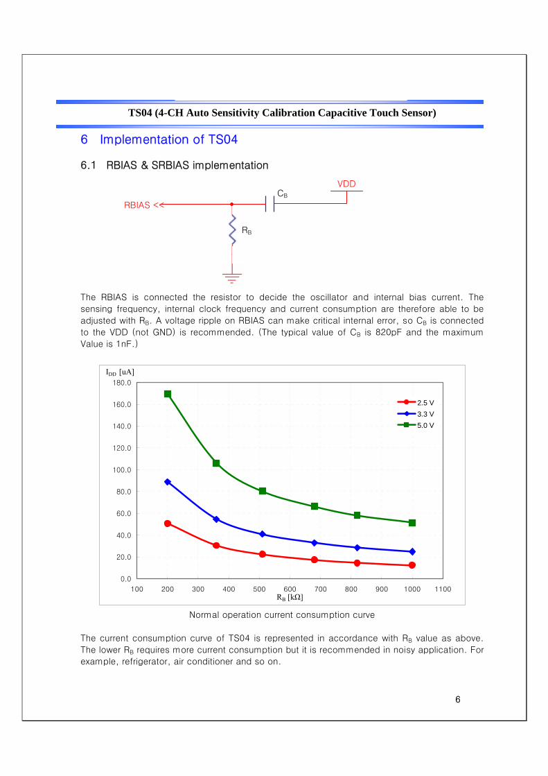
6.1 RBIAS & SRBIAS implementation
The RBIAS is connected the resistor to decide the oscillator and internal bias current. The
sensing frequency, internal clock frequency and current consumption are therefore able to be
adjusted with RB. A voltage ripple on RBIAS can make critical internal error, so CB is connected
to the VDD (not GND) is recommended. (The typical value of CB is 820pF and the maximum
Value is 1nF.)
0.0
20.0
40.0
60.0
80.0
100.0
120.0
140.0
160.0
180.0
100 200 300 400 500 600 700 800 900 1000 1100RB [kΩ]
IDD [uA]
2.5 V3.3 V5.0 V
Normal operation current consumption curve
The current consumption curve of TS04 is represented in accordance with RB value as above.
The lower RB requires more current consumption but it is recommended in noisy application. For
example, refrigerator, air conditioner and so on.
RB
CB
VDD
RBIAS <<

TS04 (4-CH Auto Sensitivity Calibration Capacitive Touch Sensor)
7
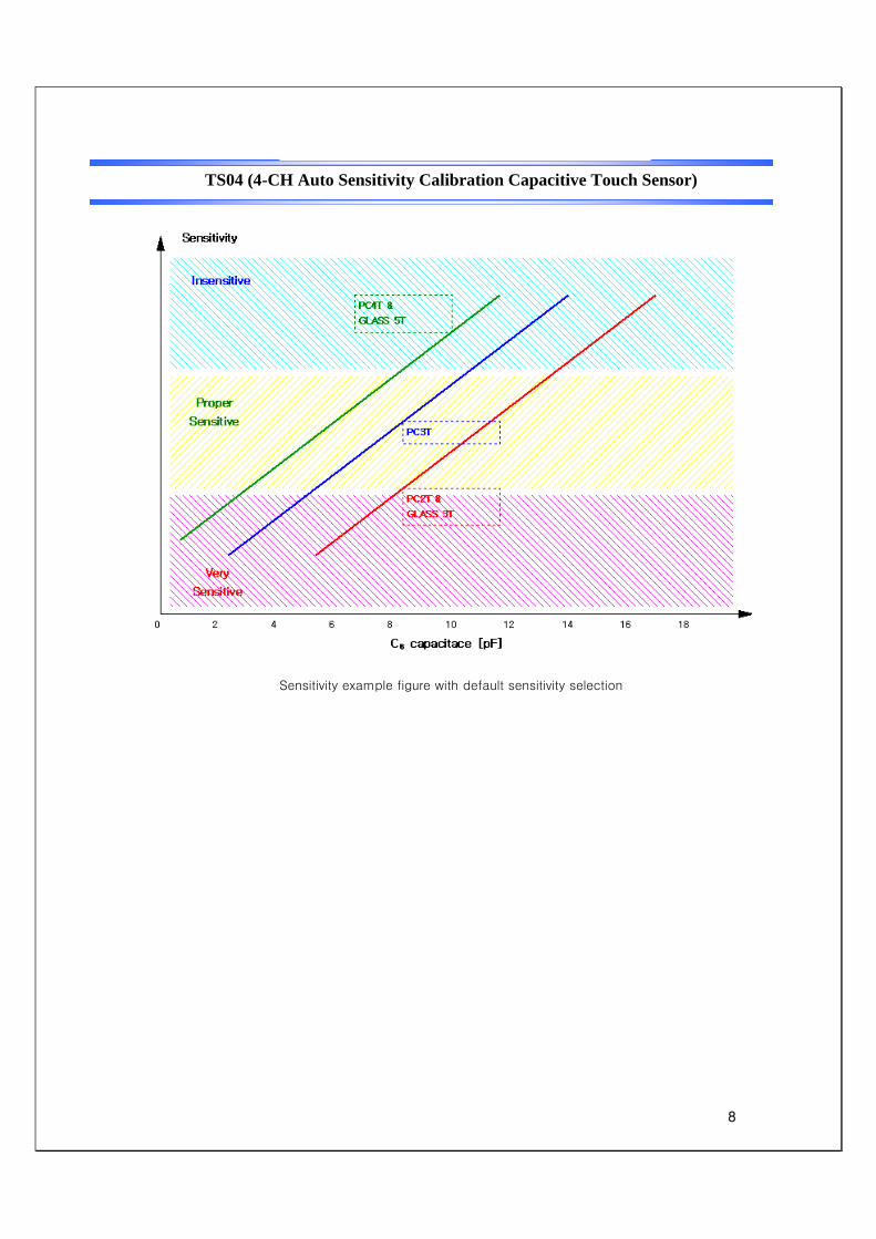
6.2 CS implementation
The TS04 has available sensing channel up to 4. The parallel capacitor CS1 is added to CS1 and
CS4 to CS4 to adjust fine sensitivity. The sensitivity would increase when a smaller value of CS is
used. (Refer to the below Sensitivity Example Figure) It could be useful in case detail sensitivity
mediation is required. The internal touch decision process of each channel is separated from
each other. The four channel touch key board application can therefore be designed by using
only one TS04 without coupling problem. The RS is serial connection resistor to avoid mal-
function from external surge and ESD. (It might be optional.) From 200Ω to 1kΩ is
recommended for RS. The size and shape of PAD might have influence on the sensitivity. The
sensitivity will be optimal when the size of PAD is approximately an half of the first knuckle (it’s
about 10 x 7 ). The connection line of CS1 ~ CS4 to touch PAD is recommended to be
routed as short as possible to prevent from abnormal touch detect caused by connection line.
There are some sensitivity difference among CS1, CS2 and CS3, and CS4 caused by internal
parasitic capacitance. That sensitivity difference could be compensated by using different CS
capacitor or sensitivity setting with internal register. To use different touch pattern area could
be used for sensitivity compensation but not recommended. The sensitivity of each channel
can be represented as below.
Sensitivity of CS1 ≥ Sensitivity of CS2, CS3 > Sensitivity of CS4
(In case of the external parasitic capacitance value is same on each channel.)
CCS1_PARA + about 3.5pF = CCS2,3_PARA + about 3pF = CCS4_PARA
* CCS1_PARA : Parasitic capacitance of CS1
* CCS2,3_PARA : Parasitic capacitance of CS2 and CS3
* CCS4_PARA : Parasitic capacitance of CS4
CS4 << Touch PAD4
CS4
CS1 <<
CS1
RS1 Touch PAD1
RS4
TS04 (4-CH Auto Sensitivity Calibration Capacitive Touch Sensor)
8
Sensitivity example figure with default sensitivity selection

TS04 (4-CH Auto Sensitivity Calibration Capacitive Touch Sensor)
9
6.3 Output Circuit Implementation
The OUTPUT pins have an open drain structure. For this reason, the connection of pull-up
resistor ROUT is required between OUTPUT and VDD. The maximum output sink current is 4mA,
so over a few kΩ must be used as ROUT. Normally 10kΩ is used as ROUT.
The OUTPUT is high in normal situation, and the value is low when a touch is detected on the
corresponding CS.
6.4 Internal reset operation
The TS04 has stable internal reset circuit to offer reset pulse to digital block. The supply voltage
for a system start or restart should be under 0.3∙VDD of normal operation VDD. No external
components required for TS04 power reset, that helps simple circuit design and to realize the
low cost application.
OUT1
ROUT1
OUTPUT1
VDD
OUT2
OUT3
OUT4
ROUT2
OUTPUT2
OUTPUT3
OUTPUT4
ROUT3
ROUT4

TS04 (4-CH Auto Sensitivity Calibration Capacitive Touch Sensor)
10
7 Recommended Circuit Diagram
7.1 Application Example (16QFN)
LED_GND
T3Pad
1Pad
N.C
.
CS410p
0
N.C.
CVDD1u
0
T1Pad
1Pad
0
TS04ADS
1
2
3
4
5 6 87
9
10
11
12
13141516
N.C.
RBIAS
GND
CS1
CS
2
CS
3
GN
D
Dum
my
CS4
OUT1
OUT2
GND
OU
T3
OU
T4
GN
D
VD
D
VDD
RS4200
0
0
RB510k
CS310p
VDD
OUT1
RO410k
RO110k
RS1200
0
0
CB820p
T4Pad
1Pad
OU
T3
T2Pad
1Pad
VDD
0
RS2200
OU
T4
CS210p
RO210k
RO310k
RS3200
CS110p
OUT2
TS04(16QFN) Application Example Circuit
In PCB layout, RB should not be placed on touch pattern. If not, CB has to be connected. The
RB pattern should be routed as short as possible. The CS patterns also should be routed as short as possible and the width of line might be
about 0.25mm (or narrower line). The capacitor that is between VDD and GND is an obligation. It should be located as close as
possible from TS04. The CS pattern routing should be formed by bottom metal (opposite metal of touch PAD). The empty space of PCB must be filled with GND pattern to strengthen GND pattern and to
prevent external noise from interfere with sensing frequency. The TS04 is reset when power rise from 0V to proper VDD

TS04 (4-CH Auto Sensitivity Calibration Capacitive Touch Sensor)
11
The VDD periodic voltage ripple over 50mV and the ripple frequency is lower than 10 kHz
can cause wrong sensitivity calibration. To prevent above problem, power (VDD, GND)
line of touch circuit should be separated from other circuit. Especially LED driver power
line or digital switching circuit power line certainly should be treated to be separated from
touch circuit.
The smaller R_B is recommended in noisy environments.
About 200Ω Resistor (RS1~RS4) and parallel capacitor (CS1~CS4) is might be inserted
to improve external noise immunity. Parallel capacitor value effects on touch sensitivity. The LED_GND and GND should be short in the system and the lines are recommended to be
split from the most low impedance ground point to avoid ground bouncing problems.
7.2 Application Example (14 SOP)
CS410p
RO210K
0
T4Pad
1 Pad
0
TS04
4
5
1
2
6
3
7 8
9
10
11
12
13
14
CS1
CS2
Gnd
VDD
CS3
Rbias
Dummy GND
CS4
OUT1
OUT2
GND
OUT3
OUT4CVDD1u
OUT1
RO310K
RS3200
0
0
OUT4
RO410K
0 0
CB820p
T3Pad
1Pad
RS1200
RB510K
VDD
RS4200
RS2200
0
OUT2
CS310p
CS210p
VDD
T2Pad
1Pad
N.C.
OUT3
RO110K
T1Pad
1Pad
CS110p
VDD
TS04(14 SOP) Application Example Circuit

TS04 (4-CH Auto Sensitivity Calibration Capacitive Touch Sensor)
12
7.3 Example – Power Line Split Strategy PCB Layout A. Not split power line (Bad power line design)
The noise that is generated by AC load or relay can be loaded at 5V power line. A big inductance might be appeared in case of the connection line between main board and
display board is too long, moreover the voltage ripple could be generated by LED (LCD) display driver at VDD (5V).
B. Split power line (One 5V regulator used) – Recommended
C. Split power line (Separated 5V regulator used) – Strongly recommended

TS04 (4-CH Auto Sensitivity Calibration Capacitive Touch Sensor)
13
8 MECHANICAL DRAWING
8.1 Mechanical drawing (16 QFN)
NOTE: Dimensions are in millimeters

TS04 (4-CH Auto Sensitivity Calibration Capacitive Touch Sensor)
14

TS04 (4-CH Auto Sensitivity Calibration Capacitive Touch Sensor)
15
8.2 Mechanical Drawing (14 SOP)

TS04 (4-CH Auto Sensitivity Calibration Capacitive Touch Sensor)
16
9 MARKING DESCRIPTION
Device Code :
Weekly Code : YY WW
Manufacturing Year Manufacturing Week
Channel Number Touch Switch Group