Embed Size (px)
Citation preview

Chip Design • www.chipdesignmag.com March �008 • 35
Interoperability GuideCadence
TRUE CIRCUITS AD

36
Cadence Interoperability Guide
Cadence Interoperability Guide www.chipdesignmag.com/cadence
CADENCE EDIT (MISSING) CADENCE EDIT (MISSING)

Cadence Interoperability Guide www.chipdesignmag.com/cadence 37www.chipdesignmag.com/cadence Cadence Interoperability Guide
Cadence Interoperability Guide
CADENCE EDIT (MISSING) CADENCE EDIT (MISSING)

38
Cadence Interoperability Guide
Cadence Interoperability Guide www.chipdesignmag.com/cadence
AMIQ
For e and SystemVerilog Development
www.dvteclipse.com
Benefits for 150Euro/seat/year
Errors as You Type
Autocomplete
Code Templates
Task Tracking
Format Source
Spell Checking
Class Browser
Semantic Search
Name Checking
Revision Control
What is DVT? DVT allows you to enjoy a modern development environment for hardware design and verification (Design and Verification Tools).
The IDE (Integrated Development Environment)approach offers significant added value over non-IDE editors. A single unified window combines the editor with the syntax checker, linter, class browser,revision control and other useful tools, enables fast and smart code development, both for beginners and complex maintenance.
DVT improves the productivity and the qualitythrough state of the art innovations: autocomplete,class browsing, task tracking, advanced search and code navigation etc.
Community is DVT onwww.eclipseplugincentral.comGet support from [email protected]
Copyright 2008 AMIQ
Eclipse and Eclipse Ready are trademarks of EclipseFoundation, Inc.

Cadence Interoperability Guide www.chipdesignmag.com/cadence 39www.chipdesignmag.com/cadence Cadence Interoperability Guide
Cadence Interoperability Guide
Apache Design Solutions
Apache Design Solutions, Inc.2645 Zanker RoadSan Jose, CA 95134USATel: 408-457-2000Fax: [email protected]
Apache’s Sentinel is the industry’s first true Chip-Package co-design/co-analysis solution for package and PCB designers. It addresses system-level power, noise, and reliability challenges for high performance, advanced package and system designs including SiPs.
Co-Design/Co-Analysis
At the core of co-design technology is the Chip Power Model (CPM), a compact spice compatible model of the full-chip power delivery network (PDN) built on the silicon-correlated RedHawk power signoff engine. CPM provides an accurate model for package and board designers to perform IC-aware package/board power and noise analyses.
By considering the impact of CPM early in the design phase, package and PCB designers can optimize their design by eliminating excess package layers, power pads, and decoupling capacitance, while maintaining its power integrity to minimize late stage design issues. During signoff, the accuracy of CPM, including on-die Power/Ground resistance, decoupling capacitance, and transistor parastics provides designers with higher degree of confidence in their package and PCB signoff.
Package/SiP Designs
Apache’s PakSi-E, a 3-D package extraction and analysis tool, is tightly integrated with Cadence’s Allegro Package Designer and SiP product lines. The embedded PakSi-E provides package designers with access to the industry’s leading 3-D package extraction technology. Through this integrated solution, designers can quickly create a full package-level simulation model that can be used to make tradeoffs among electrical and physical design requirements to meet their cost and performance targets.
For package and system designers concerned about the impact of chip’s power supply and crosstalk / jitter noise on their designs, Apache’s Sentinel product line provides a complete chip-package-system co-design/co-analysis solution for risk mitigation, cost optimization, and faster time to market.
Sentinel: Power, Noise, Reliability Platform for Chip-Package-System Co-Design
www.si2.org
• Purpose: Interoperable low-power design flows• Approach: Flow-based, user-centric, validation of standard with practical usage, supports wide range of power minimization techniques, from mobile devices to large servers• Status: CPF 1.0 Released, CPF 1.1 in process, CPF Pocket Guide available, CPF Tutorial on-line, CPF part of Reference Flow of major Fabs
level shifterisolation
retentionswitch virtual
AnalysisView
Powermode
Operatingcorner
Isolationrule
LevelShifter
Modetransition
Nominalcondition
Power Domain
Library set
Powerswitch rule
Stateretention
Libary(.lib)
BiasGndPower
ModuleInstance
Net
Ports
Pins
domain@nominal
Cell
ActivityFile
SDC
Scope Sensitivity ??
domain@corner
pwr,gnd,n-bias,p-bias
pwr,gnd
Low-Power Information Model
AMDApache DesignARMAtrentaAzuroCadenceCalyptoChipVisionEntasys Design
FreescaleGolden Gate TechnologyIBMIntelLSINXPSequence DesignSTMicroelectronicsVirage Logic
LPC Members
Low Power CoalitionLow Power Coalition

ANSYS Icemax—Parasitic Extraction Tool for Electronic Packages and Printed Circuit Boards
ANSYS® Icemax® software is an advanced parasitic extraction tool for analyzing complex integrated circuit (IC) package de-signs. The ANSYS Icemax product is based on state-of-the-art finite volume field solver technologies, which allow quick andaccurate electrical performance characterization of IC packages. Using ANSYS Icemax tools, engineers and researchersinvolved in IC package design and analysis can easily generate reliable parasitic parameters for the entire package quickly.
Fast, Accurate, 3-D Finite Volume Field SolverANSYS Icemax software uses robust and proven 3-D finite volume algorithms that reduce electromagnetic field solutiontime by several orders of magnitude. The technology is linearly scalable to multi-CPU/multi-core execution environments.Running ANSYS Icemax on multi-core 64-bit processors allows users to solve larger cases even faster.
Embedded Electrical Circuit Model GenerationUsers can run ANSYS Icemax as an engine embedded in Cadence® APD and SiP, allowing them to extract RLCG of the full package or individual subcircuits easily and fast. Models can be created in IBIS, RLCG, or subcircuit model formats forpost-layout system interconnect verification with the L and XL tiers of Allegro Package SI.
Multiple Package ConfigurationsANSYS Icemax software can handle a wide variety of package styles.• Leadframe packages, BGA packages and printed circuit boards (PCBs)• Bondwire and C4 (flipchip) packages• Stack die and other multi-die configurations• Package-on-PCB• System-in-package designs
- Combination of flipchip and bondwire designs- Package-on-package (PoP)- Package-in-package (PiP)- Combination of die-up and die-down designs
Source-to-Sink extractionUsers can place their package from Cadence APD or SiP onto a printed circuit board imported from Cadence Allegro PCBDesign within ANSYS Icemax and characterize nets from silicon to board connector. The ANSYS Icemax alignment toolmakes it easy to accurately place a package on the board, or one package on another, to create a PoP.
Easy-to-Use, Menu-Driven Modeling InterfaceThe ANSYS Icemax modeling interface is very easy to use. The software eliminates the major bottleneck in the model-build-ing process by directly importing Cadence APD, SiP or Allegro PCB Design data. Using super-fast geometry processing engines, ANSYS Icemax software works directly on industry-standard layout data and generates full 3-D numerical modelsin a matter of minutes. No special expertise or training is required for working with even the most complex package models.
Balance of Accuracy and Speed of Extraction• Quasistatic approximation to Maxwell’s equations • Hex-dominant mesh reduces mesh count • Full 3-D solver; better accuracy without compromising solution accuracy
Flexibility• Frequency update as post-processing step; no need to • Automatic ground detection; captures
rerun solution shielding effect due to ground planes • Automatic neighbor detection to set tightly coupled • Batch processing: build models first, then
subcircuits execute in batch later
OutputANSYS Icemax software will output RLCG (resistance, inductance, capacitance and conductance) in industry-standardequivalent circuit format (SPICE), matrix format (IBIS) or tabular document formats (csv, html).
©20
08 A
NS
YS
, Inc
. A
ll R
ight
s R
eser
ved.
www.ansys.com275 Technology Drive • Canonsburg, PA 15317 • USA 724.746.3304 • 1.866.267.9724
CST of America®, Inc. | To request literature or a free demo CD (508) 665 4400 | info: www.cst.com
CHANGING THE STANDARDS
Speed and accuracy blended into one. Designed to fit into the CADENCE® Allegro and APD workflow, CST harnesses the power of leading edge 3D EM full wave simulations software to study signal integrity, power integrity and EMI on your layouts.
CST MICROWAVE STUDIO® (CST MWS) is the technology leading, high performance 3D EM field simulation software. Offering true time-domain as well as frequency-domain analysis, CST MWS puts an end to the question of which tool to use. The advantages of both methods are at your disposal, separated by just one mouse click.
CST MWS’ powerful link to CADENCE® Allegro and APD facilitates the creation of full 3D structures from your layouts, including vias, BGA,
Get the flow. Enjoy your speed.
flipchip, wirebonds. The imported data will be automatically cleaned to make it suitable for 3D simulation.
Arbitrary time signals can be employed for simulation, TDR on your virtual prototype becomes an easy task. All effects such as radiated emission, electromagnetic interference and crosstalk are taken into account; for arbitrary geometries; for arbitrary frequencies. 3D EM simulation with CST MWS grants you insight into your design that measurements cannot reveal. Don’t breadboard, simulate!
CST MICROWAVE STUDIO® 2008. There’s more behind it.
CST_chip_design_cadence_03_08_v01 1 10.03.2008 09:33:04


43www.chipdesignmag.com/cadence Cadence Interoperability Guide
Cadence Interoperability Guide
Dassault Systèmes
900 Chelmsford St.Lowell, MA 01851978-442-25003DS.com
Important capabilities in the ENOVIA semiconductor solution portfolio Your design team used to be in a single department - today it’s often global. Yelling down the hallway once sufficed for collaboration, but now communication must cross borders, languages and time zones. At one time, you could survive with little or no design management in the final stages of chip development - not any more.
As the complexity facing design teams has grown, so has their need for collaboration and management for the backend of the design process. ENOVIA Synchronicity DesignSync® DFII™ adds Cadence® data recognition and processing to the standard ENOVIA Synchronicity DesignSync Design Data Management (DDM) solution. ENOVIA Synchronicity DesignSync DFII integrates into the Cadence Custom IC tool user interface and is aware of the unique file system behaviors of the Cadence software.
ENOVIA Synchronicity DesignSync manages the immense amounts of information generated from large design teams with hundreds of users. It has special features, such as data caching and mirroring to maintain performance across multiple sites, while ensuring security with LDAP
access control and SSL encryption. Detailed information on the base platform is included in the ENOVIA Synchronicity DesignSync datasheet.
ENOVIA Synchronicity DesignSync DFII is the clear industry leader for the Cadence IC community. With thousands of users across the widest customer base in the semiconductor community, IC development teams have been successfully reaping the benefits of design collaboration, IP reuse and library development and distribution as a part of their design flow. ENOVIA Synchronicity DesignSync DFII manages all kinds of data within one project and is the clear, proven choice for IC design teams and semiconductor product companies.
ENOVIA Synchronicity DesignSync DFIII
GSA Hard IP Quality Risk Assessment Tool Available for Download
The first tool in the suite, addressing hard IP quality, is available
complimentary to the industry. It enables companies to collect
important information about an IP vendor, its design methodology
and the IP under evaluation to enable risk assessment across seven
categories: IP design, integration, verification, process technology,
product documentation, reliability and test.
GSA Hard IP Licensing Risk Assessment Tool
The second Tool in the Suite, the Licensing Tool, focuses on
assessing the licensing risk an integrator is willing to accept before
acquiring the desired IP. Designed for semiconductor companies,
the Licensing Tool provides a benchmark set of questions that cover
the major areas of IP licensing and acquisition, including scope of
license, payment, warranty, limitation of liability, indemnity, governing
law, confidentiality and term and termination.
Introducing the GSA IPecosystem (IPe) Tool Suite
Future IPe Suite Tools Include: IPe Technology Risk Assessment Tool IPe Manufacturability Risk Assessment Tool
More Information: www.gsaglobal.org/ipecosystem
Tools Aid in IP Risk Assessment Process
GSA is pleased to offer a new suite of productivity tools that enables more efficient communication between IP vendors, IP integrators and foundries for IP interaction, an area critical for design success. The tools create efficiencies and lower riskby reducing the time spent collecting the specific information required to purchase, integrate and utilize IP.

44
Cadence Interoperability Guide
Cadence Interoperability Guide www.chipdesignmag.com/cadence
eInfochips
eInfochips is a valued Cadence Verification Alliance member with proven spec to silicon to system capabilities and has executed100+ complex Chip/SoC design and verification/ consultation project both onsite and offshore.
For more info on eInfochips’ products and services contact:: [email protected] , www.einfochips.com
eInfochips releases highly configurable, URM compliant HDMI UVC for verification of HDMIcompliant devices
eInfochips, Inc., a leading IP leveraged electronics design services company offering silicon design and verificationservices, IP cores and product realization services, has developed an HDMI Universal Verification Component (HDMIUVC). eInfochips’ UVC is a ready-made highly configurable, reusable, scalable and extensible verification component thatis suitable for verification of HDMI source (transmitter) and/or HDMI sink (receiver).
Top Level HDMI UVC Architecture:
Key Features:
Supports HDMI 1.3 specificationFully URM-compliant, HDL independentSupports Video Data Period, Data Island Period, Control Period, Extended Control Period Operating modesSupports Type A, Type B, Type CConnectorsSupports Display Data Channel(DDC), CEC ChannelOffers Control and Configuration of Display Data Channel(DDC),CEC ChannelBuilt-in monitors for protocolmonitoring and checking such asCharacter Synchronization bySink, High Bandwidth DigitalContent Protection(HDCP)Capable of handling Video formats such as RGB 4:4:4,YCBCR 4:2:2, YCBCR 4:4:4 atUser Configurable video encoding formats, pixel rates, format timing & frame count User configurable audio sampling frequenciesPixel Rates Ranging from below25Mhz to 680 MhzBuilt-in coverage model implemented for all transactionstypesSupports scoreboard checking Architected with ProtocolCheckers, Scoreboard, HDMISource/Sink Monitor & HDMISink & Video control libraries
Benefits:Configurable and easy to use Simplifies design verification processStandards-based for fast, easy integrationEasily compatible through highly adaptable interfacesSuperior design IP and verification IP integration shortening time to market
Deliverables:
HDMI UVC encrypted source in e-Language withSystemVerilog interface support Release notesTraining presentationUser’s Guide Test SuiteExamples of UVC usage Demos for easy feature demonstration
Applications:
The HDMI 1.3 UVC can be used in both module-level and SoC-level verification. In either test environment, the HDMI 1.3 interface of each device under test (DUT) is connected to an associatedHDMI 1.3 UVC component. Each UVC instance represents an UVC environment with a single device function.
UVC COMPLIANT VIP PORTFOLIO:PCIGbEPCI ExpressHDMII2CSPI (Serial Peripheral Interface)SONET/SDHSPI 4.2(System Packet Interface)PCI – X OCP

Cadence Interoperability Guide www.chipdesignmag.com/cadence 45www.chipdesignmag.com/cadence Cadence Interoperability Guide
Cadence Interoperability Guide
HDL Design House
HDL Design HouseMakenzijeva 79/III 11 000 BelgradeSerbiaPhone: +381 11 344 23 59Fax: +381 11 245 99 87 email: [email protected]
SoCVerify Kit is a library of HDL Design House Verification IP (VIP) with unified organization, implementation and supported verification methodologies. SoCVerify Kit is a single verification solution for SoC projects that allows verification managers to select necessary VIP from one vendor assuring that unified and advanced verification methodologies are used in all segments of SoC projects. HDL DH SocVerify Kit provides verification engineers and managers with a broad portfolio of VIP allowing easy verification of today’s SoC. With large investments in development, verification, maintenance and support for this library, HDL DH provides its customers with complete verification solutions.
SoCVerify Kit covers a large number of standards and protocols such as I2C, HyperTransport, Serial RapidIO, SATA, ATA/ATAPI, SAS, LPC, PCI, PCI-X, UART, HDMI, SPI4, SMBUS, PMBUS, JTAG, MMC, CE-ATA and VIP which constitute SoCVerify Kit library support a wide set of verification methodologies such as: eRM, UVC, OVM. HDL Design House provides to the market a multi-language verification environment and a smooth transition to advanced verification methodologies.
The purpose of SoCVerify Kit is to provide HDL Design House customers with one unified solution for SoC verification problems. Large number of supported protocols and standards by VIP in SoCVerify Kit solve typical verification problems in today’s SoC, and HDL Design House plans to include even more protocols and standards for its SoCVerify Kit VIP. Therefore, SoCVerify Kit users can count on constant improvements and enlargements of SoCVerify Kit library that will meet the requirements of each unique SoC project.
Features & Benefits:
- eRM-compliant - configurable & easy to use - URM-compliant - simplifies design verification process- SystemVerilog API provided - reduces development costs- OVM ready - speeds time-to-market with new SoCs- Transaction Based Acceleration (TBA) implemented- standards-based for fast, easy integration- vPlan with compliance tests provided- reusable in mixed language environments- benefit from a 100-1,000x increase in performance over RTL simulation- reach very high coverage with push-button ease
SoCVerify Kit by HDL Design House
Extended Evaluation Program:
HDL Design House’s SoCVerify Kit offers a broad range of VIP based on Cadence Design Verification methodologies and tools. Being longtime Cadence Verification Alliance member, HDL Design House has announced an offer for eligible users to evaluate, use and verify the quality of HDL DH UVCs from SoCVerify Kit in real SoC projects before purchase, completely free of charge. This special offer is called Extended Evaluation Program and it includes 3 month licenses for their popular UVCs along with support, with a possibility to extend the period under certain terms and conditions.
http://www.hdl-dh.com/news_item10.html
Industries served:
Consumer Products, Entertainment, Health-care, Networking, Security, Telecommunications, Wireless.
About HDL Design House:
HDL Design House specializes in rendering design and verification services for SoC projects and providing soft IP cores and verification IP (VIP) based on advanced verification methodologies such as OVM and URM. With primary focus on fulfilling each customer’s unique requirements, HDL Design House can offer design and verification services for SoC projects. In order to meet requirements of the most complex projects, HDL Design House creates dedicated engineering teams who also provide support and maintenance for VIP. The company’s high-quality and verification IP (VIP) can be easily integrated to rapidly create sophisticated verification environments for complex SoCs. The VIP program is built around advanced verification methodologies (OVM, URM) and languages (System Verilog, e). HDL Design House delivers high quality VIP with rigorous QC procedures and helps customers develop their projects by combining design and verification services and VIP portfolio. The company also delivers component (VITAL) models for major SoC product developers. Having developed more than 400 VHDL VITAL models for major memory provider companies, HDL Design House has established a reputation as a market leader in VHDL/Verilog/SystemVerilog modeling.
For additional information, please visit www.hdl-dh.com.

46
Cadence Interoperability Guide
Cadence Interoperability Guide www.chipdesignmag.com/cadence
Hummingbird
Many companies that use Cadence electronic design automation (EDA) technologies also rely on Exceed®, the industry leading PC X server, to provide the X Window environment on the latest Microsoft Windows operating systems, and offers users seamless access to the Cadence development tools. As a software solution developed by Hummingbird®, the Open Text Connectivity Solutions Group, Exceed is a reliable choice by 9 of the top 10 semiconductor companies in the world over the years.
However, with the onslaught of changes within the market, the evolution in communication technologies and a renewed business focus on reducing operational costs has posed many new challenges to the semiconductor industry….
• What if your organization is consolidating UNIX resources to central application centers that are thousands of miles away from Cadence users?
• What if your users need to reliable access Cadence from remote locations?
• What if your users want to share their work and project data with team members across the world in real-time?
How will your existing IT infrastructure manage the change? What will be the impact to your user productivity? Can you guarantee your users a secure access to Cadence development tools without significant degradation in performance all while leveraging your existing Exceed investment?
Exceed Freedom™ is the solution…
Resource Consolidation
Instead of replicating IT infrastructure when setting up worldwide design center, a growing number of semiconductor companies are creating capable application centers in strategic locations. All projects are centrally stored and managed in those centers for all developers and engineers to access. With its unique architecture and up to 100 times network bandwidth reduction, Exceed Freedom allows users to securely and efficiently access application centers in any part of the world.
Resiliency to Failures
How many times have you had a user panicking on the phone because their computer was rebooted after a mandatory Windows Update? As a result, the Exceed session was gone, along with the design project that the user had been working on for the past four hours.
The Crash and Resume feature of Exceed Freedom shields your users from many unexpected and unpleasant system and network failures by keeping their sessions alive in a middle-tier server. Your users’ value projects are protected.
Hummingbird®: Pushing the Limits of Cadence Applications and Exceed Users
Real-time Collaboration
With design centers and engineers scattered all over the world working on the same project, extensive collaboration amongst all stakeholders is critical. Exceed Freedom can instantly add collaborative capabilities to any UNIX application without modification. Through its Desktop Sharing feature, Exceed Freedom users from different development centers can share Exceed sessions and design ideas in real-time. Moreover, IT staff can shadow user’s sessions, visualize and troubleshoot their problems on-the-fly. Exceed Freedom helps improve communication efficiency and reduce your time-to-market
Leveraging Existing Exceed Configuration
Exceed Freedom is designed for Exceed so it works right out-of-the-box. Installation is driven by industry standard Windows Installer technology. There are little post-deployment configuration requirements because Exceed Freedom reuses existing Exceed configuration files, which are the culmination of many hours of customer support and “tweaking.” Users do not have to be re-trained and the IT support group will not be flooded with an increased volume of support incidents, as it would likely be with any other new software roll-out. There is no break-in period and no downtime. Exceed Freedom is a no-risk choice for improving productivity and security, and reducing downtime
About Hummingbird
To obtain more information about Exceed Freedom, please visit www.hummingbird.com to download a free evaluation, whitepaper, business & technical solution overview and press release.
To learn more about how Hummingbird
has been successful with
semiconductor companies please go to
www.hummingbird.com/cadence under Success Stories.
www.hummingbird.com | [email protected] | 905-762-6400

Cadence Interoperability Guide www.chipdesignmag.com/cadence
48
Cadence Interoperability Guide
Cadence Interoperability Guide www.chipdesignmag.com/cadence
MunEDA
MunEDAMunEDA WiCkeDTM: Improve Design Performance and Yield
MunEDA provides leading EDA technology for analysis and optimization of yield and performance of analog, mixed-signal and custom digital designs. MunEDA’s products and solutions enable customers to reduce the design time of their circuits and to maximize robustness and yield. MunEDA’s tools are in industrial use in the areas of communication, computer, memories, automotive, and consumer electronics by leading semiconductor companies worldwide and proven in more than 1000+ design and tape-out projects.
MunEDA was founded in 2001 and is a privately held company. The company headquarter is located in Munich, Germany. MunEDA has offices in Munich, Germany (Headquarter) and Sunnyvale, California, USA (MunEDA Inc.).
MunEDA is represented by leading EDA distribution companies worldwide in USA, Japan, Korea, Taiwan, Singapore, Malaysia, Scandinavia, and others (see the Contact section on www.muneda.com).
WiCkeDTM DFM-DFY Tool Overview WiCkeDTM is a comprehensive and powerful interactive software tool suite for manual, semi- and fully automatic analysis and optimization of performance, robustness and yield as well as performance modelling of analog and mixed-signal circuits.
WiCkeDTM includes tools and methodologies for - Topology Analysis & Optimization - Nominal Performance Analysis & Optimization - Yield Analysis & Optimization - Response Surface Modelling
Picture: MunEDA WiCkeDTM Tools Overview
WiCkeDTM can be operated either through a graphical user interface or through a programmable scripting interface (batch mode).
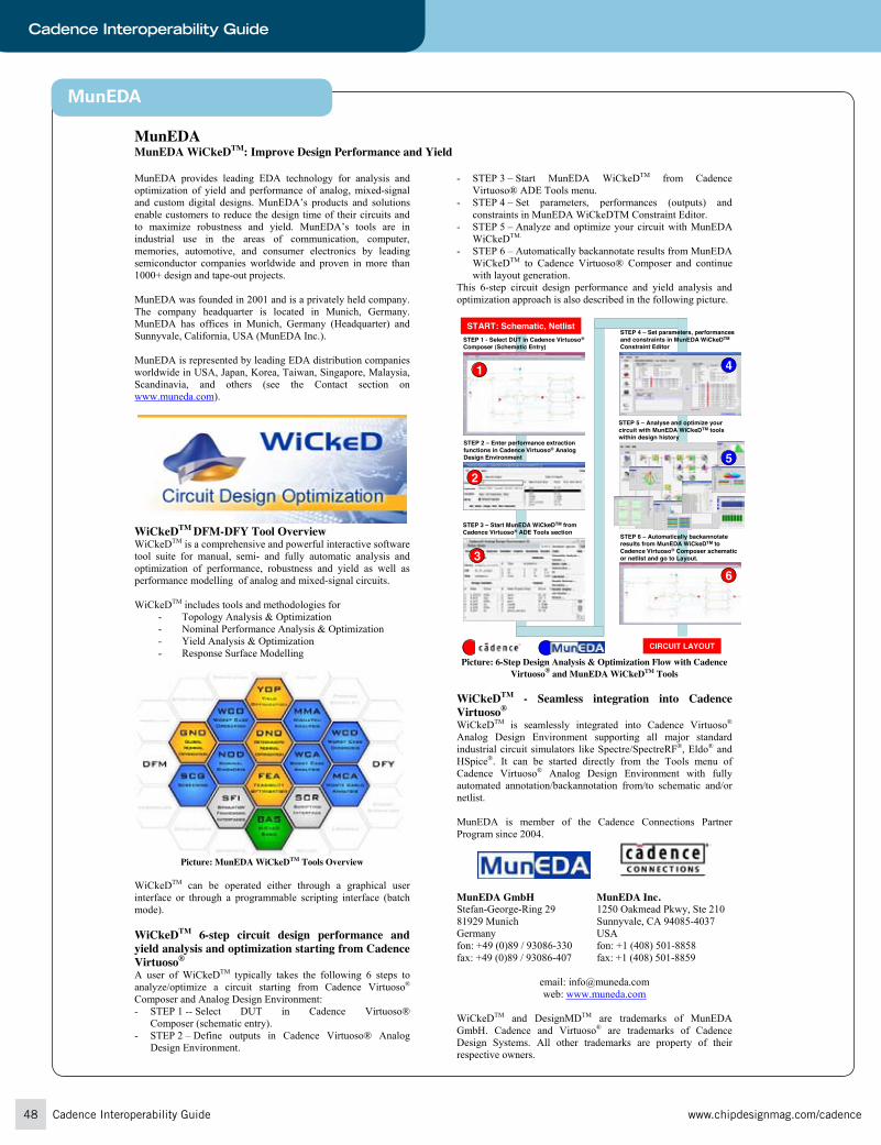
WiCkeDTM 6-step circuit design performance and yield analysis and optimization starting from Cadence Virtuoso®
A user of WiCkeDTM typically takes the following 6 steps to analyze/optimize a circuit starting from Cadence Virtuoso®
Composer and Analog Design Environment: - STEP 1 -- Select DUT in Cadence Virtuoso®
Composer (schematic entry). - STEP 2 – Define outputs in Cadence Virtuoso® Analog
Design Environment.
- STEP 3 – Start MunEDA WiCkeDTM from Cadence Virtuoso® ADE Tools menu.
- STEP 4 – Set parameters, performances (outputs) and constraints in MunEDA WiCkeDTM Constraint Editor.
- STEP 5 – Analyze and optimize your circuit with MunEDA WiCkeDTM.
- STEP 6 – Automatically backannotate results from MunEDA WiCkeDTM to Cadence Virtuoso® Composer and continue with layout generation.
This 6-step circuit design performance and yield analysis and optimization approach is also described in the following picture.
STEP 1 - Select DUT in Cadence Virtuoso®
Composer (Schematic Entry)
STEP 2 – Enter performance extractionfunctions in Cadence Virtuoso® Analog Design Environment
STEP 3 – Start MunEDA WiCkeDTM fromCadence Virtuoso® ADE Tools section
STEP 4 – Set parameters, performancesand constraints in MunEDA WiCkeDTM
Constraint Editor
STEP 6 – Automatically backannotateresults from MunEDA WiCkeDTM toCadence Virtuoso® Composer schematicor netlist and go to Layout.
STEP 5 – Analyse and optimize yourcircuit with MunEDA WiCkeDTM toolswithin design history
START: Schematic, Netlist
CIRCUIT LAYOUT
2
1
3
4
5
6
Picture: 6-Step Design Analysis & Optimization Flow with Cadence Virtuoso® and MunEDA WiCkeDTM Tools
WiCkeDTM - Seamless integration into Cadence Virtuoso®
WiCkeDTM is seamlessly integrated into Cadence Virtuoso®
Analog Design Environment supporting all major standard industrial circuit simulators like Spectre/SpectreRF®, Eldo® and HSpice®. It can be started directly from the Tools menu of Cadence Virtuoso® Analog Design Environment with fully automated annotation/backannotation from/to schematic and/or netlist.
MunEDA is member of the Cadence Connections Partner Program since 2004.
MunEDA GmbH MunEDA Inc. Stefan-George-Ring 29 1250 Oakmead Pkwy, Ste 210 81929 Munich Sunnyvale, CA 94085-4037 Germany USA fon: +49 (0)89 / 93086-330 fon: +1 (408) 501-8858 fax: +49 (0)89 / 93086-407 fax: +1 (408) 501-8859
email: [email protected] web: www.muneda.com
WiCkeDTM and DesignMDTM are trademarks of MunEDA GmbH. Cadence and Virtuoso® are trademarks of Cadence Design Systems. All other trademarks are property of their respective owners.

Cadence Interoperability Guide www.chipdesignmag.com/cadence
Nangate’s Design Optimizer™ is the re-synthesis solution for next-generation physical design flows. The Design Optimizer brings together standard-cell library creation with gate-level optimization to provide significant improvements in design speed, area and power consumption.
RTL Synthesis and Physical Design flows from leadingsuppliers all rely on a predefined, fixed standard-cell library. Standard-cell libraries are created with the intent ofgeneral-purpose usage across various design types, so compromises have to be made that affect performance on a particular design. The Design Optimizer removes these restrictions and introduces concurrent optimization of design and library, resulting in speed gains of 10-20% or area and power gains of 10-30%, depending on the design’s ratio of combinational to sequential logic cells.
The Nangate Library Creator™ enables digital CMOS IC designers to custom-tailor digital cell libraries and to explore the impact of alternate device models, design rules and cell architectures. The Library Creator enables minute control of individual cell attributes, enabling custom cell libraries which enhance performance beyond the capabilities of commercially available libraries.
Nangate’s Library Characterizer™ is an ultra-fast, all-inclusive package for accurate characterization of digital cell libraries. It includes a powerful Spice-based characterization engine with fully automated stimulus generation, a library model checker and a databook generator. Characterized libraries can be qualified against test circuits to ensure Spice-level accuracy and correlation with Static Timing Analysis.
155-A Moffett Park Drive, Suite 101Sunnyvale, CA 94089-1321Phone: +1 (408) 541-1992
www.nangate.com
Nangate Physical Re-synthesis Flow
NANGATE - THE DESIGN OPTIMIZATION COMPANYNangate’s EDA tools and silicon IP benefit IC designers by providing lower power consumption,reduced manufacturing costs, higher chip performance, improved manufacturability and shorter time to market.

www.novas.com
Genius at work
Spare time provided by Novas
Genius is working smarter—not harder.
Genius is spending time adding value to designs—instead of debugging.
Genius is a verification methodology without extra runs for recording results.
Genius is getting designs done on time without giving up the rest of your life.
Novas is quite literally, accelerating engineers.
How will you use the extra time?
Faster Debug—Enhanced Visibility—Better Verification
ACCELERATING ENGINEERS
SERIES_Dad_Kid 6/23/06 2:39 PM Page 1

51www.chipdesignmag.com/cadence Cadence Interoperability Guide
Cadence Interoperability Guide
Perception Software
Perception Software105 W. Riverside Dr.Suite 100Austin, TX 78704USATel: 512.472.1700www.perceptionsoftware.comsales@perceptionsoftware.com
The goal of EDAConnect -SIP is to enable to rapid integration of the SiP design process within a company’s total system design process. Time to market pressures and the time/resource costs of process updates dictate a streamlined approach to the total product design environment. To address this, many companies have invested in product lifecycle management (PLM) systems to keep track of the product record, manage design changes, and manage release to manufacturing. To be most effective in integrating the package design process with the enterprise, the solution must be implemented to tightly couple PLM tasks with the Package Design tasks as to not extend design cycle time or place undue burdens on design engineers. EDAConnect-SIP accomplishes this by understanding both the design environment as well as enterprise PLM practices with respect to roles, permissions and business processes. EDAConnect-SiP provides a window to data held in enterprise PLM systems for the engineer at the point-of-decision during design creation. Package designers are provided a view of PLM that is relevant to package design process, allowing them to collaborate in an efficient and controlled fashion with IC design and manufacturing, as well as PCB designers, while managing and tracking changes. This cross-domain cooperation results in an efficient system design process and enterprise visibility of the total end product. With a single click EDAConnect-SIP can update PLM with the current configuration of the SiP and populate required PLM objects with characteristics extracted from the SIP design databases. Timely and accurate data insures PLM is kept current with latest versions of the critical design and manufacturing files.
EDAConnect-SIP uses a template approach to consistently drive design publishing. This enables a wide set of data to be transferred with minimal interaction from the engineer. Secure, accurate, and accessible design data will help drive collaboration between IC and package design teams, as well as help minimize errors and cycle time with the manufacturing chain. Engineering work requests contain information that generally needs to be re-entered in the CAD system with outputs manually associated with the original request. EDAConnect-SiP intercepts these requests and sends data creation parameters directly to the design environment. Upon completion of the work request EDAConnect-SIP creates all necessary PLM data items with searchable attributes and attaches data files in one step. In addition EDAConnect-SIP also provides additional benefit for the IC designer by allowing the publishing of package critical design files to PLM and automatically notifications routed to the package designer of the update. This allows the die designer to release design data quickly to the enterprise PLM system so that downstream engineering processes can begin.
EDAConnect-SiP

52
Cadence Interoperability Guide
Cadence Interoperability Guide www.chipdesignmag.com/cadence
PLDA
PLDAParc du Golf Bât. 11A Rue Guillibert13856, Aix-en-ProvencePhone: +33 442 393 600Fax: +33 442 394 902 email: [email protected]
PLDA designs and sells a wide range of FPGA and ASIC IP interfacing solutions for the high speed bus market. Profitable since its inception in 1996, PLDA is privately owned and has reported increasing profits for the last seven years. Our success is based on doing one thing very well—Intellectual Property Cores (and related boards) for ASICs, Structured-ASICs, and FPGAs. We provide solutions for the following high speed bus interfaces:
• PCI Express 2.0• PCI Express • PCI-X • PCI • AXI-PCI Express• AHB-PCI Express
PLDA has been an OpenChoice Cadence partner for many years. Our leading edge IP products include support for Cadence simulation tools and formal verification tools. You can use PLDA PCIe IP products with confidence, knowing that:
• PLDA has the most PCI designs in the industry today. With over 500 FPGA and ASIC designs in layout and production, PLDA is the go-to resource for PCI IP and prototyping boards.
PLDA – Premier PCIe IP Products featuring Support for Cadence Tools
• PLDA has a strong history with Cadence. We have provided critical IP products for many joint designs. PLDA prides itself on delivering the best support in the industry, so you can rest assured that your design will be on-time and on-budget.
• PLDA is uniquely focused on PCI. With an offering that includes ASIC, FPGA and Structured ASIC products, you will have the flexibility you need during product development to design quickly using an FPGA prototype and then seamlessly transition to an ASIC for cost advantages.
Evaluate PlDa PCie iP free for 30 days and let us show you why PlDa is your PCie resource center for Cadence users.
The Online Network Dedicated to the Needs of the Advanced IC Design Market
Visit www.chipdesignmag.com
Latest News
Focus Reports
Blogs
White Papers andProduct Information
Interoperability Guides
High Value Feature Articles
Resource Center Essential Tools

Cadence Interoperability Guide www.chipdesignmag.com/cadence 53www.chipdesignmag.com/cadence Cadence Interoperability Guide
Cadence Interoperability Guide
Virage Logic Corporation
Virage Logic is the preferred supplier of semiconductor IP solutions to the global semiconductor industry providing a broad portfolio of silicon proven physical IP products targeted at the world’s leading foundry processes from 250- to 45nm and application specific IP for DDR memory interface solutions. Silicon Aware IP™ Incorporating silicon behavior knowledge for increased predictability and manufacturability Physical IP Solutions SiWare™ Memory Power-Optimized Memories for Advanced Processes at 65nm and 45nm SiWare™ Logic Yield-Optimized Standard Cells for a Wide Variety of Design Applications at 65nm and 45nm ASAP™ Memory Self-Test Enabled High-Density, High-Speed and Ultra-Low-Power Memories ASAP™ Logic Metal Programmable, Standard Cell, Ultra-Low-Power and ECO Libraries STAR™ Memory Embedded Memories Designed for Testability and Manufacturability to Optimize Yield STAR™ Memory System Self-Test and Repairable Memories STAR™ Yield Accelerator Reduces Silicon Time-to-Test, Time-to-Product Bring-Up, Time-to-Volume Production NOVeA® NVM on a Standard CMOS Process IPrima® Foundation Optimized Platforms for Specific Technology Nodes and Foundry Processes Foundry Pays IP Silicon Proven Foundry Pays Free IP – in Partnership with Leading Foundries Worldwide Base I/O Libraries Rich Set of I/O Cells Intelli™ DDR High Performance and Low Latency Memory Controllers for DDR1/DDR2/DDR3 Based Systems Low Power,
Semiconductor IP Solutions
High Bandwidth Memory Controller for MobileSDR and Mobile DDR Based Systems Application Specific IP Solutions Intelli™ PHY+DLL Physical Layer Interface + DLL Hard Macro Solution for DDR1/DDR2/DDR3 Based Systems Intelli™ PHY Physical Layer Interface Companion for Intelli DDR Products Intelli™ DLL High Precision, Small Footprint, Digital Delay Locked Loop Intelli™ Models Vendor Independent Simulation Models for DDR Memories
Virage Logic Corporation47100 Bayside ParkwayFremont, CA 94538USAPhone: 510-360-8000Toll Free: 1-800-524-0133Fax: 510-360-8089 [email protected]
The Online Network Dedicated to the Needs of the Advanced IC Design Market
Visit www.chipdesignmag.com
Latest News
Focus Reports
Blogs
White Papers andProduct Information
Interoperability Guides
High Value Feature Articles
Resource Center Essential Tools

54
Cadence Interoperability Guide
Cadence Interoperability Guide www.chipdesignmag.com/cadence
Innovator in Pattern Conversion, Validation, and Retargeting Technologies since 1979 Debugging and verifying test patterns after first silicon is an inefficient and expensive process, especially when your test teams or test partners report failing patterns in test-centric terminologies. This results in cost overruns and significant delays in the IC development cycle.
TSSI tools help design and verification engineers to generate ATE-ready test patterns and validate them on a virtual test model of their target ATE. Pre-, and post-silicon test programs can be validated or debugged by simulating them with the DUT model in the same design environment.
TSSI VirtualTester (TVTTM)TVT minimizes the time and resources needed to debug and verify test program files by providing design and test engineers with a workstation-based model of their target ATE. The same design environment for the DUT model can be added with the target ATE model. Test programs can be simulated as if on the tester without further conversion back to testbench format to avoid potentially introducing new variations.
TVT’s Powerful Debug Features and Benefits: Automated tester-device connection Source line numbers retained throughout “Micro-probes”. Virtually no physical accessibility limitation to internal nodes Activity log with pattern labels and microcode annotations for easy correlation Error log of all compare mismatches On-the-fly pattern editing and masking enables “What-if” debug processes Waveform display of ATE system status and user selected device pins Seamless interface with industry leading Verilog and VHDL simulators Retargeting one ATE program to another enables flexible ATE utilization and early selection with confidence IEEE 1450 STIL Standard Based Architecture enables ATE-neutral validation for enterprise standardization of design-to-test methodology Layered architecture enables scalability and extendibility into future capabilities including mixed signal validation Simulation and Tester Errors Comparison
Typical Silicon Big Up Issues Detected by TVT:
Timing Errors – due to device initialization, tester rules violation, resource allocation, etc Read/Write Register Tests Fail on the Tester – due to reversed bit sequenceI/O Contention Non-Functional Patterns – typically due to translation errors
TSSI’s Pattern Conversion Tools Help Generate Accurate Test Patterns, Fast! TDS (Test Development Series)
With the largest installed base, TDS is the enterprise strength tool suite since the 80’s and has contributed to the industry the de facto standard Waveform Generation Language (WGL) in its heavily used WaveMaker module. TDS supports 30+ EDA formats and 90+ ATE models
TestDeveloper Family (TD, TDSim, and TDScan) This Windows-based product suite is scalable, and most portable for pattern conversion teams to get their job done anywhere, anytime. TD products support VCD, EVCD, WGL, STIL and all leading ATE models from Advantest, Credence, LTX, Verigy, and Teradyne.
Visit Us Online at: www.tessi.com
14789 SW Millikan Way Beaverton, Oregon 97006 USA
DesignTestBench
Tester-ReadyFiles
VirtualTester
SCB
TSSI Conversion Tools: TDS, TD, TDSim, TDScan
Other Conversion Tools
Finished ATE Programs
ATPG or Functional STIL
Re-simulates Tester Output Files “as is”. No additional conversion. Different
ATEPlatforms
Retargeting

Cadence Interoperability Guide www.chipdesignmag.com/cadence
Just One Click!
ZELAND SOFTWARE, INC.48834 Kato Road, Suite 103A, Fremont, CA 94538, U.S.A.,
Tel: 510-623-7162 Fax: 510-623-7135 E-mail: [email protected] functional free evaluation license available from www.zeland.com
Layered polygons in GDSII or other IC and PCB layout formats
Full 3D model with ports defined and ready for simulation on IE3D
Just One Click!
You can actually go directly into IE3D simulations of a batch of GDSII files with a single click of button.
From IC and PCB Layouts to IE3D Full-Wave EM ResultsFor the design of microwave circuits, MMIC, RFIC, LTCC, RFID, IC Interconnects, PCB,MCM, SoP, SIP, antennas, signal and power integrity & other high frequency applications
IE3D 14 features integrated EM design environment with FastEM Design Kit for real-timeEM tuning, optimization and synthesis and covering frequency range from 1 Hz to 10 THz
Just One Click!
Just One Click!
Automatic EM Simulation on IE3D from GDSII Layouts
RFIC EM Simulation on IE3D from Cadence Virtuoso
PCB EM Simulation on IE3D from Cadence Allegro/APD
Real-Time Full-Wave Spiral and RFIC Synthesis on IE3D
High Performance EM Simulation and Optimization and Electronic Design Automation

Over the past decade, the evolution of radio design for wireless communications has accelerated to accommodate the
demands of communications standards and systems. Commercial cellular standards, for example, have transitioned from all-analog, single-channel FM, AMPS-based systems to the currently proposed multi-channel, 100-Mbps, orthogonal frequency division multiple access (OFDMA) -based fourth-generation (4G) systems. Today’s military and homeland-security applications heavily leverage these commercial wireless developments. After all, they’re seeking to rapidly deploy secure multi-format, multiband radios.
These demands have driven commercial suppliers of silicon-based signal-processing systems to new levels of integration, power consumption, and speed. State-of-the-art silicon-based, signal-processing engines can handle thousands of MIPS in milliWatt-power-consumption ranges. Meanwhile, commercial silicon-based data-converter technology is driving higher sample rates with very high dynamic ranges.
The implication is clear: It’s now possible to deploy high-performance, multi-format, multiband radios without the need for a costly and complex analog-radio front end. In effect, the analog-to-digital converter (ADC) is moving closer to the antenna than was previously possible. The results are true software- and firmware-defined radios. The achieved adaptability and flexibility in tactical radio is driving down the cost of new system deployment. At the same time, design and test requirements for these systems have become much more demanding. Big rewards await the engineer who does it right while huge hits await the designer who misses something.
SDR DEVELOPMENT CHALLENGESIt is becoming more important for developers of software-defined-radio (SDR) architectures to utilize development tools that can carry their designs from early algorithm development all the way through to prototype/hardware test and verification. Today, many different methodologies are employed in the design of SDRs—each with its own merits and detractors. Some methodologies, for example, provide extraordinary engineering efficiencies for the individual or small group. But they lack the portability required for larger groups or enterprise development. Others utilize high-level language constructs, but lack the low-level capability needed for transferring IP to hardware.
SDR development must also support multiple wireless signaling formats and validate system performance under demanding signal conditions. Many man years have been invested to address this challenge, yet new waveform types appear every day. The demand for additional new-waveform development continues to drive resource and budget decisions.
SDR Development Challenges Are RevealedA VIABLE ALTERNATIVEDevelopers of SDR architectures require tools and methodologies that allow the rapid design and prototyping of potential designs. They also must permit the creation of virtual waveform libraries, which accurately represent commercial-off-the-shelf (COTS) signals. These tools and methodologies should allow for the easy customization of COTS signals to include interference and implementation impairments of the given SDR architecture. As the complexity of waveforms and SDR architectures grow, it is increasingly important for these tools and methodologies to be easy to use, support highly portable intermediate design output (e.g., VHDL and ANSI-C), and enable the easy creation of waveform libraries that can flow from early design all the way to design validation.
These virtual waveform libraries will allow SDR developers to create scenarios that simulate performance of their SDR architectures. Thus they can wring out potential shortcomings in compatibility or performance before committing to a design. This includes modeling today’s crowded spectral environments with multiple waveform types occupying the same frequency bands—something the developer would not want to find out about after the product has been deployed to the commercial market or battlefield. At that point, it’s simply too late.
Virtual waveform libraries also can allow for actual hardware system measurements and validation. Once the developer has committed to an architecture, it is highly desirable to validate radio performance using the same stringent ssignaling scenarios that were created during the design phase. This enables final validation of SDR-architecture performance using actual hardware prototypes and raises the developer’s confidence that the system will work in actual deployment.
Today, SDR concepts are being realized in part due to improvements in technology stemming from commercial and defense-oriented SDR development. As a result, developers now face many challenges including the ability to design and validate the performance of their SDR architectures against COTS signaling formats. These SDR developers require powerful, easy-to-use tools and methodologies that bring their designs through deployment quickly. In doing so, they should ensure both performance and compatibility with each of these signal waveforms.
Jim McGillivary is the vice president and general manager of Agilent EEsof EDA. McGillivary joined Hewlett-Packard Company in 1986 as a hardware and software development engineer.
More gates, more speed, more versatility, and of course, less cost— it’s what you expect from The Dini Group. This new board features 16 Xilinx Virtex-5
LX 330s (-1 or -2 speed grades). With over 32 Million ASIC gates (not counting memories ormultipliers) the DN9000K10 is the biggest, fastest, ASIC prototyping platform in production.
User-friendly features include:
• 9 clock networks, balanced and distributed to all FPGAs
• 6 DDR2 SODIMM modules with options for FLASH, SSRAM, QDR SSRAM, Mictor(s),DDR3, RLDRAM, and other memories
• USB and multiple RS 232 ports for user interface
• 1500 I/O pins for the most demanding expansion requirements
Software for board operation includes reference designs to get you up and running quickly. Theboard is available “off-the-shelf ” with lead times of 2-3 weeks. For more gates and more speed,call The Dini Group and get your product to market faster.
www.dinigroup.com • 1010 Pearl Street, Suite 6 • La Jolla, CA 92037 • (858) 454-3419 • e-mail: [email protected]� • March �008
By Jim Mcgillivary nO respIns

More gates, more speed, more versatility, and of course, less cost— it’s what you expect from The Dini Group. This new board features 16 Xilinx Virtex-5
LX 330s (-1 or -2 speed grades). With over 32 Million ASIC gates (not counting memories ormultipliers) the DN9000K10 is the biggest, fastest, ASIC prototyping platform in production.
User-friendly features include:
• 9 clock networks, balanced and distributed to all FPGAs
• 6 DDR2 SODIMM modules with options for FLASH, SSRAM, QDR SSRAM, Mictor(s),DDR3, RLDRAM, and other memories
• USB and multiple RS 232 ports for user interface
• 1500 I/O pins for the most demanding expansion requirements
Software for board operation includes reference designs to get you up and running quickly. Theboard is available “off-the-shelf ” with lead times of 2-3 weeks. For more gates and more speed,call The Dini Group and get your product to market faster.
www.dinigroup.com • 1010 Pearl Street, Suite 6 • La Jolla, CA 92037 • (858) 454-3419 • e-mail: [email protected]

iv • March �008 Chip Design • www.chipdesignmag.com
New TimingDesigner® 9.0 Design KitsLike placing an actual DDR2 right into your design
Timing
PCB
SI
Custom IC
Analog
Digital
Libraries
Mechanical
PLM
Training {
Design kits save design timeImagine placing DDR2 memory directly into yourtiming analysis. Or an FPGA. Or a processor. No searchingfor specifications and no time wasted. The new design kits forTimingDesigner are pre-assembled component diagrams completewith all specified libraries for speed and voltage ratings. They provideall documented timing protocols associated with one or more designcomponents. They are assembled for easy import into TimingDesignerallowing quick assembly of any timing project.
Wide variety of kitsDesign Kits are available for a variety of processors, various memory stylessuch as DDR2 and Flash, and interface specifications like PCI-Express andUSB. They give you that time saving head start for accurate timing analysis.
Boost your productivity with TimingDesigner 9.0 today!For more information about TimingDesigner call EMA at 800.813.7288 orvisit us online at www.timingdesigner.com/kits
©2007 EMA Design Automation, Inc. All rights reserved in the U.S. andother countries. TimingDesigner is a registered trademarks of EMA DesignAutiomation, Inc. Cadence is a registered trademarks of Cadence DesignSystems, Inc.All other marks are the property of their respective owners.
EMA_TD 9.0_DDR_Chip_Design.qxp:Layout 1 11/16/07 11:05 AM Page 1