Embed Size (px)
Citation preview

1SLUA783–October 2016Submit Documentation Feedback
Copyright © 2016, Texas Instruments Incorporated
Troubleshooting TI PSR Controllers
Application ReportSLUA783–October 2016
Troubleshooting TI PSR Controllers
KeningGao
ABSTRACTPower supply designers must often troubleshoot problems. The problems may include smoke upon firstsupplying power or the device displays no light or noise and does not start up at all. The fundamentals ofdebugging should be to make sure the components are assembled correctly according to the schematicwith no incorrect PCB connections[1]. This document focuses on the design issues and assumes the boardhas been checked and that failed components have been repaired. This application note can be used forTI’s primary-side regulated (PSR) controllers and switchers, such as the UCC2870X, UCC2871X,UCC2872X, UCC28730, and UCC2891X.
Contents1 Background ................................................................................................................... 22 Issue 1: Power Converter Cannot Startup or Shuts Down Unexpectedly ............................................ 3
2.1 Cause 1: VDD UVLO ................................................................................................ 32.2 Cause 2: VDD Clamp Current Exceeding Rating (Only for UCC2891X)...................................... 32.3 Cause 3: VIN UVLO ................................................................................................. 32.4 Improper BJT Selection ............................................................................................ 42.5 Cause 4: On-time Detection ....................................................................................... 52.6 Cause 5: CS Short Circuit (1.5-V) Protection ................................................................... 62.7 Cause 6: AUX Winding Detection (OVP) ........................................................................ 7
3 Issue 2: Output Voltage Ripple and Noise is Quite High at Certain Load............................................ 83.1 Is That a Line Frequency Ripple? ................................................................................ 83.2 Is that a low frequency oscillation (loop unstable for TI PSR)?............................................... 8
4 Issue 3: Transient Response Worse ...................................................................................... 94.1 PSR Limitation ...................................................................................................... 9
5 Issue 4: Constant Current Mode........................................................................................... 95.1 CC Value Varies With High or Low Line Input .................................................................. 9
6 Issue 5: Missing Valley Switching ......................................................................................... 96.1 Cause 1 - LC Resonant Period Too Long ....................................................................... 96.2 Cause 2 - Very Quick Resonant Decay With TVS Snubber ................................................. 10
7 Issue 6: Audible Noise..................................................................................................... 108 Device Nomenclature ...................................................................................................... 119 Other Support Resources ................................................................................................. 1210 References .................................................................................................................. 12
List of Figures
1 Simplified Typical TI PSR Flyback Application .......................................................................... 22 VDD UVLO Protection ........................................................................................................ 33 Waveforms Needed to Distinguish Input UVLO Issue .................................................................. 44 UVLO Protection Caused by Improper BJT Selection .................................................................. 55 Startup Issue Caused by Long tON on a UCC28704 Board............................................................. 56 OCP Caused by the Noise ................................................................................................. 67 OCP Protection Caused by Transformer Saturation .................................................................... 78 B-H Temperature Characteristics of the TDK PC95 .................................................................... 79 Line Frequency Ripple in Output Voltage ................................................................................ 8

+
-VAC
CB1 CB2 NP
RSTR
VAUX
NA RS1
RS2
CDD
RCBC
GND
CBC
VS
VDD
UCC28700SOT23-6
NS
VF+ -
DRV
CS
RCS
RLS
COUT
RPL
VBLK
Copyright © 2016, Texas Instruments Incorporated
Background www.ti.com
2 SLUA783–October 2016Submit Documentation Feedback
Copyright © 2016, Texas Instruments Incorporated
Troubleshooting TI PSR Controllers
10 Higher Output Ripple With Approximate kHz Oscillation ............................................................... 911 Long LC Resonant Period Causes Missing Valley Switching ........................................................ 1012 Very Quick Resonant Decay Caused by Improper Snubber Design ................................................ 10
1 BackgroundTable 1 is a comparison table for TI’s PSR controllers and switchers. Minor differences are noted eventhough the control laws and working principles may be similar.
Table 1. Comparison Table for TI PSR Parts
TI PSR Part HV Start Output Drive forUCC2870X No MOSFETUCC2871X Yes MOSFETUCC28720 Yes BJTUCC28722 No BJTUCC28730 Yes MOSFETUCC2891X Yes Integrated MOSFET
Figure 1 is a simplified basic reference circuit used for description purposes in this application note. Notethe part used in Figure 1 is the UCC28700. If using other parts, there are minor differences in the circuitthat will not affect troubleshooting. Also note that primary and secondary snubbers are not shown.
Figure 1. Simplified Typical TI PSR Flyback Application

VVDD(off)
VVDD(on)
DRV
VDD
IC output pulses until VDDOFF
www.ti.com Issue 1: Power Converter Cannot Startup or Shuts Down Unexpectedly
3SLUA783–October 2016Submit Documentation Feedback
Copyright © 2016, Texas Instruments Incorporated
Troubleshooting TI PSR Controllers
2 Issue 1: Power Converter Cannot Startup or Shuts Down Unexpectedly
2.1 Cause 1: VDD UVLOPhenomenon: Before VDD goes down to VVDD(off), there are switching pulses with which the frequency ishigher than minimum frequency, Fsw(min), as shown in Figure 2.
Figure 2. VDD UVLO Protection
Potential Solutions:• Increasing the auxiliary winding turns will elevate the VDD level.• Increase VDD capacitance. This helps the VDD sustain time also helping with startup.• Decrease output capacitance and increase the constant current point. See the “primary side regulation”
on the datasheet for the constant current. A simple way to increase the constant current point is todecrease the RCS resistor. These methods increase the rising time of Vout to help startup.
• Decrease the resistor in-series with an auxiliary diode, if any. It will elevate the VDD level by collectingmore leakage energy of the transformer with some load.
• “Full Load, CC Mode, load-on point = 0 V” is the serious configuration of E-load for startup. Sometimeschanges on the E-load configuration, such as setting half load or CR Mode or setting load-on point athigher value, are acceptable within the system requirements.
2.2 Cause 2: VDD Clamp Current Exceeding Rating (Only for UCC2891X)Phenomenon: VDD reaches VDDCLP (minimum 26 V), and the clamp flowing current exceeds 6 mA[2].
Potential Solutions: Make sure VDD stays lower than VDDCLP at all conditions by setting the Na/Nsproperly and adjusting the resistor in-series with VDD diode.
2.3 Cause 3: VIN UVLOTI PSR parts have AC-line input undervoltage protection functions by detecting current information at theVS pin during the MOSFET on-time. While the VS pin is clamped close to GND during the MOSFET on-time, the current through RS1 is monitored to determine a sample of the bulk capacitor voltage[4]. To makesure the converter works properly, the VS dividers should be designed carefully according to thedatasheet.

Issue 1: Power Converter Cannot Startup or Shuts Down Unexpectedly www.ti.com
4 SLUA783–October 2016Submit Documentation Feedback
Copyright © 2016, Texas Instruments Incorporated
Troubleshooting TI PSR Controllers
However, if you believe the calculation is right, but there is a shutdown or startup issue, capture the lastthree cycles of VBLK, VAUX, and VDRV as is suggested in Figure 3. Determine the root cause by checking thefollowing:1. Is the voltage of VBLK too low? — A bulk capacitor value that is too small would make the ripple on VBLK
too much, especially at low-line input and full load. A rough suggestion for bulk capacitor selection isabout 2 µF / W. For a 10-W design, 22-µF capacitance (22 µF is standard value) is suggested.
2. Is the VAUX waveform flat and the VAUX approach to VBLK × Na / Np during MOSFET on-time? — If not,there is something wrong; check the transformer turns ratio and the voltage on the primary windingsduring Q1 on-time. A common issue is Improper BJT Selection.
3. Is the current from the VS pin at startup (for the issues where there are only three cycles of pulses)VAUX / RS1 larger than IVSL(run)? — Make sure the current is larger than IVSL(run), or else go back check therelated parameters.
4. Is the current from the VS pin at the last switching cycle (for the issues where there are many cycles)VAUX / RS1 lower than IVSL(stop)? — If yes, it will cause the converter to shut down.
Figure 3. Waveforms Needed to Distinguish Input UVLO Issue
2.4 Improper BJT SelectionFor UCC28722 and UCC28720 devices, improper selection for BJT could cause the input UVLOprotection. The BJT may not be fully switched on due to the low current gain. VAUX during MOSFET on-time is not flat and does not match VBLK × Na / Np near the end of MOSFET on-time. Figure 4 shows atypical UVLO protection caused by improper BJT selection.
An important parameter for a BJT is hFE, DC current gain. It varies with IB, VCE and temperature and canbe quite low. For the UCC2872X application, base current IB is decided by the controller’s driving currentIDRS (19 mA to 37 mA).
So the hFE current gain of BJT should be high enough to make the BJT operate with lower on-state VCE.

www.ti.com Issue 1: Power Converter Cannot Startup or Shuts Down Unexpectedly
5SLUA783–October 2016Submit Documentation Feedback
Copyright © 2016, Texas Instruments Incorporated
Troubleshooting TI PSR Controllers
Figure 4. UVLO Protection Caused by Improper BJT Selection
2.5 Cause 4: On-time Detection
2.5.1 On-Time is Too Long at First Startup CyclePhenomenon: TI PSR controllers and switchers check the MOSFET on-time by detecting the voltage onthe CS pin on the very first cycle after VDD UVLO on. If the voltage on the CS pin does not reach IPP(min) inthe desired time, the IC will confirm the fault and discharge VDD to VVDD(off) where IPP(min) = VCST(min) / RCS. ForUCC28704 and UCC28730, this desired time is typical 4 µs. For UCC28700/1/2/3, UCC28710/1/2/3,UCC28720/2, UCC28740 the desired time for tON fault is 1 / FSW(max). As for the first cycle, tON = (LPRI × IPRI) /VBLK, too high inductance or very low input voltage can cause this startup issue. Figure 5 shows the tONfault of the UCC28704 circuit.
Potential Solutions: To verify the issue, increasing input voltage, decreasing LPRI or increasing RCS canbe used. However, the circuit designer should check the power system design completely to find out whythe tON time is so large.
Right side of image is zooRight side of image is zoomed in, tON is larger than 4 µs.
Figure 5. Startup Issue Caused by Long tON on a UCC28704 Board
2.5.2 Too Long On-Time Causes ShutdownPhenomenon: This is only suited for the UCC2891X. The IC will stop DRV output and start the VDD UVLOcycle when it detects three consecutive on-times larger than tONMAX(max) at high load and tONMAX(min) at lightload.
Potential Solutions: To verify the issue, decrease LPRI or increase RIPK. However, the circuit designershould check the power system design completely to find out why the tON time is so large.
CCRPK
IPK
VI
R=
( )CST max
PRI
CS
V
IR
=
PRI PRIMAX
P
L IB
N Ae
´
=
´
Issue 1: Power Converter Cannot Startup or Shuts Down Unexpectedly www.ti.com
6 SLUA783–October 2016Submit Documentation Feedback
Copyright © 2016, Texas Instruments Incorporated
Troubleshooting TI PSR Controllers
2.6 Cause 5: CS Short Circuit (1.5-V) ProtectionThe converter will stop the switching cycle and start a VDD reset cycle when the IC detects a voltage onthe CS pin higher than 1.5 V for three consecutive cycles.
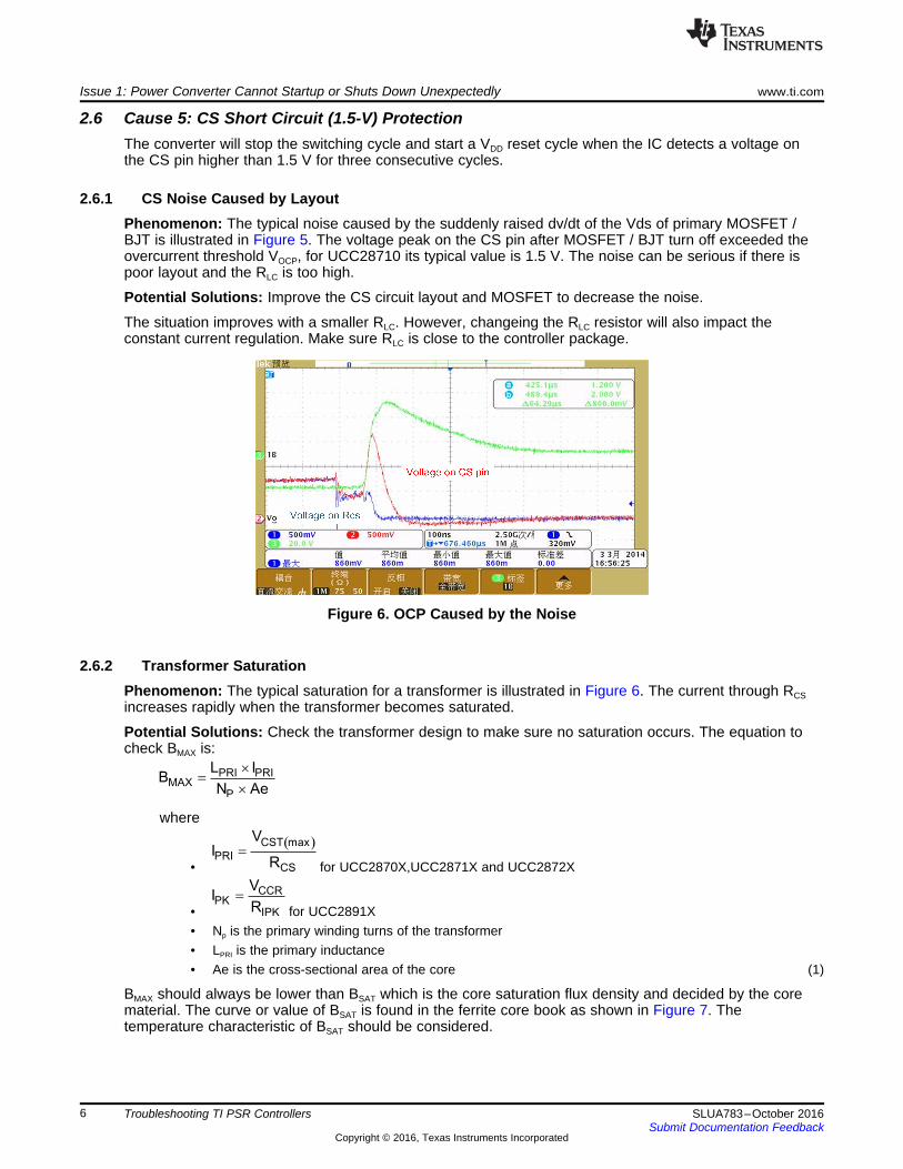
2.6.1 CS Noise Caused by LayoutPhenomenon: The typical noise caused by the suddenly raised dv/dt of the Vds of primary MOSFET /BJT is illustrated in Figure 5. The voltage peak on the CS pin after MOSFET / BJT turn off exceeded theovercurrent threshold VOCP, for UCC28710 its typical value is 1.5 V. The noise can be serious if there ispoor layout and the RLC is too high.
Potential Solutions: Improve the CS circuit layout and MOSFET to decrease the noise.
The situation improves with a smaller RLC. However, changeing the RLC resistor will also impact theconstant current regulation. Make sure RLC is close to the controller package.
Figure 6. OCP Caused by the Noise
2.6.2 Transformer SaturationPhenomenon: The typical saturation for a transformer is illustrated in Figure 6. The current through RCSincreases rapidly when the transformer becomes saturated.
Potential Solutions: Check the transformer design to make sure no saturation occurs. The equation tocheck BMAX is:
where
• for UCC2870X,UCC2871X and UCC2872X
• for UCC2891X• Np is the primary winding turns of the transformer• LPRI is the primary inductance• Ae is the cross-sectional area of the core (1)
BMAX should always be lower than BSAT which is the core saturation flux density and decided by the corematerial. The curve or value of BSAT is found in the ferrite core book as shown in Figure 7. Thetemperature characteristic of BSAT should be considered.

Magnetic field H(A/m)
Flu
x de
nsity
B(m
T)
0 200 400 600 800 1000 1200 1400 16000
100
200
300
400
500
600
D001
25 qC60 qC100 qC120 qC
VCS
VDRV
Transformer became saturated
www.ti.com Issue 1: Power Converter Cannot Startup or Shuts Down Unexpectedly
7SLUA783–October 2016Submit Documentation Feedback
Copyright © 2016, Texas Instruments Incorporated
Troubleshooting TI PSR Controllers
Figure 7. OCP Protection Caused by Transformer Saturation
Figure 8. B-H Temperature Characteristics of the TDK PC95
2.7 Cause 6: AUX Winding Detection (OVP)The output overvoltage function is determined by the voltage feedback on the VS pin. The device stopsswitching and starts to discharge the VDD capacitor to the VVDD(off) threshold when it detects an overvoltage.
2.7.1 Output Voltage Trigger OVP at Zero LoadPhenomenon: When probing on the output voltage, the output voltage exceeds the regulation level andthe voltage reflected to the VS pin exceeds the overvoltage threshold VOVP.
Potential Solutions: Decrease the capacitance of the drain node, which mainly includes the COSS of theMOSFET and input capacitance of the transformer;• To decrease the preload resistor value• To check if the turn-off of the MOSFET is too slow which may cause too large of a series resistor in the
gate
2.7.2 The Shape on the VS Pin Affects the DetectionThe PSR controller does not sense the output directly like a traditional optocoupler feedback. It is moresensitive by its working scheme of detecting the auxiliary winding voltage. The shape of the voltage on theVS pin is very important to avoid mis-detection and OVP. Because probing on the VS pin could also affectthe detection, estimate the waveform of the VS pin by probing the auxiliary winding.
See the respective datasheet for the needed shapes.

Issue 2: Output Voltage Ripple and Noise is Quite High at Certain Load www.ti.com
8 SLUA783–October 2016Submit Documentation Feedback
Copyright © 2016, Texas Instruments Incorporated
Troubleshooting TI PSR Controllers
However, snubber adjusting especially on the damping resistor can affect the waveforms. A leakageinductance of the transformer that is too high would make the detection less accurate. The layout of theVS relative circuit should also be done correctly. The trace between the VS dividers and the VS pin shouldbe as short as possible to reduce EMI coupling[4].
3 Issue 2: Output Voltage Ripple and Noise is Quite High at Certain LoadFirst of all, check if the converter is in VDD UVLO reset and restart sequence. If the VDD crosses betweenVVDD(on) and VVDD(off), which will cause ripple issues, the protection is triggered. From issue 1, you could getclues to find out and solve the root cause. If the VDD does not hiccup between VVDD(on) and VVDD(off)thresholds, then proceed to debug with one of the following tips:
3.1 Is That a Line Frequency Ripple?Figure 9 is a typical waveform of high ripple with line frequency. When VBLK is at a lower point, theconverter cannot provide enough power to the output, so the “Dip” ripple may be seen. To solve thisproblem, increasing the bulk cap or decreasing the Np/Ns ratio can be used. However, as changing theNp/Ns also affects other performance, checking the calculation according to the datasheet is the root wayto solve this issue.
Figure 9. Line Frequency Ripple in Output Voltage
3.2 Is that a low frequency oscillation (loop unstable for TI PSR)?The closed-loop of PSR is not as apparent as it is of opto-feedback. So if there is unexpected ripple withseveral kHz frequency (not the line frequency) as shown in Figure 10, investigate the following points:• Check if there is a missing valley switching, as mentioned in Issue 5: Missing Valley Switching. The
abnormal valley switching could cause some oscillation on the ripple.• The loop instability could cause high ripple. As it is difficult to measure the closed loop response in
PSR parts, the way to mitigate it is to increase the output capacitor and increase the working frequencyat full load.
• Noise on the VS and CS pin can also have an effect on the instability.

PRIperiod 2 L Csw= p ´
www.ti.com Issue 3: Transient Response Worse
9SLUA783–October 2016Submit Documentation Feedback
Copyright © 2016, Texas Instruments Incorporated
Troubleshooting TI PSR Controllers
Figure 10. Higher Output Ripple With Approximate kHz Oscillation
4 Issue 3: Transient Response Worse
4.1 PSR LimitationThe PSR has a limitation of the transient response, especially when the load is switched from light load tohalf load or full load. This is because the switching frequency is very low at light load.
For special cases which need better transient response when the load switches from zero load to a certainload, increasing the working frequency of zero load and increasing the output capacitor can work. But,increasing the working frequency of a zero load also means a higher preload requirement whichdeteriorates standby power.
Another choice is using the UCC28730+UCC24650 chipset solution, which brings both very low standbypower and a good transient response performance.
5 Issue 4: Constant Current Mode
5.1 CC Value Varies With High or Low Line InputPhenomenon: The CC greatly varies with different line input voltage.
Potential Solutions: Adjusting the RLC resistor should mitigate the difference. See the respectivedatasheet for the function of the RLC resistor.
6 Issue 5: Missing Valley SwitchingThe PSR controllers and switchers from TI operate in discontinuous conduction mode with valley-switching to minimize switching losses. However, improper design could make the valley switchingdisappear, which could cause increased switching loss and higher ripple or higher noise.
6.1 Cause 1 - LC Resonant Period Too LongPhenomenon: The LC resonant tank exceeded the tZTO. tZTO is defined as zero crossing timeout delay andis specified in datasheet. For UCC2870X, UCC2871X and UCC2891X, the minimum value of tZTO is 1.8µs, for the UCC28730 it is 1.6 µs. As the resonant frequency is decided by the primary inductance of thetransformer and equivalent capacitor on the drain node CSW = COSS + CW (where COSS is the outputcapacitance of primary MOSFET and Cw is the transformer capacitance), the resonant
.
Potential Solutions: Decrease the primary inductance IPRI or capacitance on the drain node to solve thisissue.

Issue 5: Missing Valley Switching www.ti.com
10 SLUA783–October 2016Submit Documentation Feedback
Copyright © 2016, Texas Instruments Incorporated
Troubleshooting TI PSR Controllers
Figure 11. Long LC Resonant Period Causes Missing Valley Switching
6.2 Cause 2 - Very Quick Resonant Decay With TVS SnubberPhenomenon: When very low standby power is required and switching frequency is very low, a TVSsnubber must be used. With a TVS snubber, improper selection of slow clamp diode will cause a veryquick decaying as shown in Figure 12. For a detailed explanation of this issue, see Choosing StandardRecovery Diode or Ultra-Fast Diode in Snubber (SNVA744).
Potential Solutions: An R2CD snubber is suggested to replace the TVS snubber for those which do notneed very low standby power applications; If a TVS snubber is a must, using ultra-fast diode in a snubbercircuit or paralleling small capacitor on TVS.
Figure 12. Very Quick Resonant Decay Caused by Improper Snubber Design
7 Issue 6: Audible NoiseThe audible noise of flyback is usually caused by ceramic capacitors or the ferrite transformer because ofmechanical vibration.
If replacing the ceramic capacitors, which have high dv/dt swings (such as snubber cap), with a metal-filmcapacitor and dip-varnishing the transformer does not work, an improper design must be considered asthe problem. Engineers should check the output stability (Issue 2: Output Voltage Ripple and Noise isQuite High at Certain Load) .
Another way to mitigate the audible noise is to make the converter work in the highest frequency allowedby the part’s datasheet.

www.ti.com Device Nomenclature
11SLUA783–October 2016Submit Documentation Feedback
Copyright © 2016, Texas Instruments Incorporated
Troubleshooting TI PSR Controllers
8 Device NomenclatureDevice Terms
VVDD(off) UVLO turn-off voltage (see the electrical characteristics table of the respective datasheet)VVDD(on) UVLO turn-on voltage (see the electrical characteristics table of the respective datasheet)VDDCLP VDD voltage clamp (see the electrical characteristics table of the UCC28910, UCC28911
datasheet (SLUS769))VCST(min) CS pin minimum current-sense threshold (see the electrical characteristics table of the
respective datasheet)VCST(max) CS pin maximum current-sense threshold (see the electrical characteristics table of the
respective datasheet)VOCP Overcurrent threshold (see the electrical characteristics table of the respective datasheet)VCCR Constant-current regulating voltage (see the electrical characteristics table of the
respective datasheet)VOVP Overvoltage threshold (see the electrical characteristics table of the respective datasheet)FSW(min) Minimum switching frequency (see the electrical characteristics table of the respective
datasheet)FSW(max) Maximum switching frequency (see the electrical characteristics table of the respective
datasheet)IVSL(run) VS line-sense run current (see the electrical characteristics table of the respective
datasheet)IVSL(stop) VS line-sense stop current (see the electrical characteristics table of the respective
datasheet)IDRS DRV source current (see the electrical characteristics table of the respective datasheet)tONMAX(max) Maximum FET on time at high load (see the electrical characteristics table of the
UCC28910, UCC28911 datasheet (SLUS769))tONMAX(min) Maximum FET on time at low load (see the electrical characteristics table of the
UCC28910, UCC28911 datasheet (SLUS769))tZTO Zero-crossing timeout delay (see the electrical characteristics table of the UCC28910,
UCC28911 datasheet (SLUS769))
BJT Terms
VCE Collector-emitter voltagehFE DC current gainIB Base current
Transformer Terms
Na/Ns Auxiliary-to-secondary turns ratioNa/Np Auxiliary-to-primary turns ratioNp/Ns Primary-to-secondary turns ratioLPRI Primary inductanceBSAT Saturation flux density
Other Support Resources www.ti.com
12 SLUA783–October 2016Submit Documentation Feedback
Copyright © 2016, Texas Instruments Incorporated
Troubleshooting TI PSR Controllers
Other Terms
RIPK UCC28910, UCC28911 primary current programming resistanceRLC Line compensation resistorRS1 High-side VS pin resistanceRCS Primary current programming resistanceCOSS Output capacitance of MOSFETCw Total capacitance on the switching nodeTON On-time of MOSFET / BJTIPRI Peak primary current
9 Other Support ResourcesMore help is available from TI's E2D forum:https://e2e.ti.com/support/power_management/isolated_controllers/
10 References1. Robert Taylor, Ryan Mannack, Debugging power-supply startup issues, Analog Applications Journal,
3Q-20152. UCC28910, UCC28911 datasheet (SLUS769)3. Kening Gao, Ulrich B. Goerke, Choosing Standard Recovery Diode or Ultra-Fast Diode in Snubber, TI
application note (SNVA744)4. UCC2870x datasheet (SLUSB41)

IMPORTANT NOTICE
Texas Instruments Incorporated and its subsidiaries (TI) reserve the right to make corrections, enhancements, improvements and otherchanges to its semiconductor products and services per JESD46, latest issue, and to discontinue any product or service per JESD48, latestissue. Buyers should obtain the latest relevant information before placing orders and should verify that such information is current andcomplete. All semiconductor products (also referred to herein as “components”) are sold subject to TI’s terms and conditions of salesupplied at the time of order acknowledgment.TI warrants performance of its components to the specifications applicable at the time of sale, in accordance with the warranty in TI’s termsand conditions of sale of semiconductor products. Testing and other quality control techniques are used to the extent TI deems necessaryto support this warranty. Except where mandated by applicable law, testing of all parameters of each component is not necessarilyperformed.TI assumes no liability for applications assistance or the design of Buyers’ products. Buyers are responsible for their products andapplications using TI components. To minimize the risks associated with Buyers’ products and applications, Buyers should provideadequate design and operating safeguards.TI does not warrant or represent that any license, either express or implied, is granted under any patent right, copyright, mask work right, orother intellectual property right relating to any combination, machine, or process in which TI components or services are used. Informationpublished by TI regarding third-party products or services does not constitute a license to use such products or services or a warranty orendorsement thereof. Use of such information may require a license from a third party under the patents or other intellectual property of thethird party, or a license from TI under the patents or other intellectual property of TI.Reproduction of significant portions of TI information in TI data books or data sheets is permissible only if reproduction is without alterationand is accompanied by all associated warranties, conditions, limitations, and notices. TI is not responsible or liable for such altereddocumentation. Information of third parties may be subject to additional restrictions.Resale of TI components or services with statements different from or beyond the parameters stated by TI for that component or servicevoids all express and any implied warranties for the associated TI component or service and is an unfair and deceptive business practice.TI is not responsible or liable for any such statements.Buyer acknowledges and agrees that it is solely responsible for compliance with all legal, regulatory and safety-related requirementsconcerning its products, and any use of TI components in its applications, notwithstanding any applications-related information or supportthat may be provided by TI. Buyer represents and agrees that it has all the necessary expertise to create and implement safeguards whichanticipate dangerous consequences of failures, monitor failures and their consequences, lessen the likelihood of failures that might causeharm and take appropriate remedial actions. Buyer will fully indemnify TI and its representatives against any damages arising out of the useof any TI components in safety-critical applications.In some cases, TI components may be promoted specifically to facilitate safety-related applications. With such components, TI’s goal is tohelp enable customers to design and create their own end-product solutions that meet applicable functional safety standards andrequirements. Nonetheless, such components are subject to these terms.No TI components are authorized for use in FDA Class III (or similar life-critical medical equipment) unless authorized officers of the partieshave executed a special agreement specifically governing such use.Only those TI components which TI has specifically designated as military grade or “enhanced plastic” are designed and intended for use inmilitary/aerospace applications or environments. Buyer acknowledges and agrees that any military or aerospace use of TI componentswhich have not been so designated is solely at the Buyer's risk, and that Buyer is solely responsible for compliance with all legal andregulatory requirements in connection with such use.TI has specifically designated certain components as meeting ISO/TS16949 requirements, mainly for automotive use. In any case of use ofnon-designated products, TI will not be responsible for any failure to meet ISO/TS16949.
Products ApplicationsAudio www.ti.com/audio Automotive and Transportation www.ti.com/automotiveAmplifiers amplifier.ti.com Communications and Telecom www.ti.com/communicationsData Converters dataconverter.ti.com Computers and Peripherals www.ti.com/computersDLP® Products www.dlp.com Consumer Electronics www.ti.com/consumer-appsDSP dsp.ti.com Energy and Lighting www.ti.com/energyClocks and Timers www.ti.com/clocks Industrial www.ti.com/industrialInterface interface.ti.com Medical www.ti.com/medicalLogic logic.ti.com Security www.ti.com/securityPower Mgmt power.ti.com Space, Avionics and Defense www.ti.com/space-avionics-defenseMicrocontrollers microcontroller.ti.com Video and Imaging www.ti.com/videoRFID www.ti-rfid.comOMAP Applications Processors www.ti.com/omap TI E2E Community e2e.ti.comWireless Connectivity www.ti.com/wirelessconnectivity
Mailing Address: Texas Instruments, Post Office Box 655303, Dallas, Texas 75265Copyright © 2016, Texas Instruments Incorporated
![YQLW Qt UR]P U velikosti.pdfpsr 73/74/79/1 25 psr 140/160/1 75 psr 21 5/225 psr 260/270/280/290 psr 295/340/350 psr 540/550/730/740 psr 1000/2000 psr 1500/3000/8000 psr 9000 psr a300](https://img.dokumen.tips/doc/110x75/5e2699892211d34f32527d31/yqlw-qt-urp-u-psr-7374791-25-psr-1401601-75-psr-21-5225-psr-260270280290.jpg)


![Инструкция Yamaha PSR-E453PSR-E453/PSR-EW400 7 + " , . 4 " [ ] ( 5 .) ( 6&- " ), " . $ , . # "](https://img.dokumen.tips/doc/110x75/60dceb7003bf806879693103/f-yamaha-psr-e453-psr-e453psr-ew400-7-4-.jpg)