Embed Size (px)
Citation preview

TRIPLE TRACK Delta ASIC WITH SHIFT-OUT
ROHS COMPLIANT
SPECIFICATIONS
Specification Part Number 99875336 Rev 1
DECEMBER 2005
An ISO 9001 Registered Company
1710 Apollo Court Seal Beach, CA 90740 Phone: (562) 546-6400 FAX: (562) 546-6301
Technical Support: (651) 415-6800 www.magtek.com
ii
Copyright© 2001-2005 MagTek®, Inc.
All Rights Reserved Printed in the United States of America
Information in this document is subject to change without notice. No part of this document may be reproduced or transmitted in any form or by any means, electronic or mechanical, for any purpose, without the express written permission of MagTek, Inc. MagTek is a registered trademark of MagTek, Inc. MLF is a trademark of AmkorTM, Inc.
REVISIONS
Rev Date Notes 1 8 Dec 05 Initial Release based on 99875259-12. Corrected example connector part
numbers. Added specification for head cleanliness. Added notes about additional head loading, unused tracks, and head load for sensitivity measurements. Further clarified WDT operation. Basically removed errata section. Removed “Considerations for New Designs…” section.

iii
TABLE OF CONTENTS
INTRODUCTION .................................................................................................................................................1 FEATURES..........................................................................................................................................................1 CONFIGURATIONS ............................................................................................................................................2 SHIFT-OUT PROTOCOL – ISO FORMAT CARDS AND MOST OTHERS ........................................................3 SHIFT-OUT TIMING ............................................................................................................................................7 PREAMBLE KEY .................................................................................................................................................9 SHIFT-OUT PROTOCOL– CARDS ALLOWING 13 OR MORE CONSECUTIVE ZERO-BITS IN THE DATA FIELD ..............................................................................................................................................10 RECOMMENDATIONS AND PRECAUTIONS FOR MECHANICAL DESIGN .................................................12
Technical Specifications ................................................................................................................................13 PACKAGING AND DRAWINGS ........................................................................................................................14
Packaging and Pin Assignments ...................................................................................................................14 Mechanical Drawings ....................................................................................................................................14
PRINTED CIRCUIT BOARD LAYOUT RECOMMENDATIONS AND SCHEMATICS ......................................17 General Guidelines........................................................................................................................................17 IntelliHead......................................................................................................................................................17 MLFTM-14 with Provision for Shift-Out IntelliHeadTM......................................................................................19 Recommended PCB Land Pattern for the MLFTM-14 Package.....................................................................21
ERRATA.............................................................................................................................................................22 Products Affected ..........................................................................................................................................22 Details............................................................................................................................................................22
TABLE OF FIGURES AND TABLES
Figure 1. Timing ................................................................................................................................................ 7 Table 1. Signal and Pin Assignments – Triple Track ASIC ............................................................................ 14 Figure 2. Package Marking for 21006529....................................................................................................... 15 Figure 3. Package Marking for 21006539....................................................................................................... 16 Figure 4. PCB Layout...................................................................................................................................... 19 Figure 5. Schematic ........................................................................................................................................ 20 Figure 6. Recommended PCB Land Pattern .................................................................................................. 21

iv
(This page left blank)

1
INTRODUCTION MagTek is pleased to offer a high-performance low-cost three-channel fully integrated magnetic stripe decoder chip or ASIC (Application Specific Integrated Circuit). This innovative, yet low-cost card reading solution offers many important advantages over the conventional less-integrated approach. Packaged in a 14 pin MLFTM (MicroLeadFrameTM), this miniaturized Triple-Track Delta ASIC provides a “Shift-Out” protocol for extracting data that significantly simplifies the card-reader to micro-controller interface. In addition to the 14 pin MLFTM Packaged Triple-Track ASIC as a stand-alone chip, MagTek also offers the Shift-Out IntelliHead, a magnetic head with the chip actually built-in. The Shift-Out IntelliHead uses the same Triple-Track ASIC, but completely encapsulated in a low-profile magnetic head, offering further integration and excellent noise immunity by shielding the low-level analog signals inside the head. Unless your application dictates the use of a particular separate or custom magnetic head, MagTek recommends the Shift-Out IntelliHead for best performance, best miniaturization, and best economy. See MagTek specification 99875258 for information on the Shift-Out IntelliHead product family. For applications that can limit the supply voltage to the ASIC to 3.6V, the 21006540/41 ASIC is recommended instead of the 21006529/39 ASIC described in this manual. The 21006540/41 ASIC is a newer chip that will provide reduced power consumption and additional features at a reduced cost. It is also available integrated into a head as part of the Shift-Out IntelliHead product family. See MagTek specification 99875337 for information on this newer ASIC. FEATURES
• Low cost solution for single, dual, or triple track readers – one triple-track chip works for all • Compact design – 4 mm x 5mm 14 pin MLFTM (also called QFN) surface mount package
• Minimal external components – only a decoupling capacitor is required. Only 2 signals, DATA,
and STROBE, to connect to your micro-controller for up to 3 tracks
• Data buffer with Shift-Out – allows full card data to be locally stored on ASIC. Retrieve when desired. Use a low-cost controller with no interrupts, limited memory, low-speed, low pin-count, etc.
• High noise immunity – with proper PCB layout, the ASIC can withstand noisy PC monitors, cell
phones, switching power supplies, etc.
• High performance decoding – reads badly damaged cards; compensates for poor head mounting
• Low voltage operation – 2.8 Vdc to 5.5 Vdc
• Low operating current – less than 4 mA maximum total current at 3.3V (for up to 3 tracks) while card is being swiped
• Ultra-low Sleep current – less than 75 μA maximum total current when no card is being swiped

Triple Track ASIC
2
• AGC (Automatic Gain Control) – reads cards from 30% - 200% of International Standards Organization (ISO) 7811 amplitude standard
• Wide operational temperature range – -40° C to +85° C
• Wide range of card swipe speeds – from 2.5 to 100 in/s (6.3 to 254 cm/s) for the standard 75 to
210 bits per inch (bpi) data density1
• RoHS Compliant – “lead (Pb) free” component
CONFIGURATIONS Part Number Description 21006529 ASIC, Triple Track, F/2F Decode, MLF14, RoHS-compliant, Tube 21006539 ASIC, Triple Track, F/2F Decode, MLF14, RoHS-compliant, Tape and Reel Note: The 21006529 and 21006539 are equivalent to the now obsolete 21006536 and 21006537
respectively, except the newer parts are RoHS-compliant (“Pb-free”).
1 The actual minimum instantaneous card speed allowed is 4.7cm/s (1.85ips) using zero-jitter 75bpi data; however, there is a whole card timeout of 1.35s minimum, yielding a whole card average speed lower limit of approximately 6.3cm/s (2.5ips).

Triple Track ASIC
3
SHIFT-OUT PROTOCOL – ISO FORMAT CARDS AND MOST OTHERS The magnetic-stripe card formats most commonly used, including the ISO format, do not allow 13 consecutive zero-bits to occur in the actual data field. This section of the specification applies to only these commonly occurring cards. If your application requires the reading of custom-data-formats that do allow 13 consecutive zero-bits to appear in the data-field (excluding the “leading” and “trailing” zero-bits), then refer to the “SHIFT-OUT PROTOCOL – CARDS ALLOWING 13 OR MORE CONSECUTIVE ZERO-BITS IN THE DATA FIELD” section located near the end of this specification. DATA is the sole output of the ASIC and is normally held high. Once the ASIC has qualified a head signal as a magnetic stripe card, it begins to store data from the card in its buffer. In general, after the card is read, the DATA line transitions from high to a low level (ZEROES FLAG) indicating the Buffer-Ready state. This falling edge of DATA is the signal to a micro-controller that the on-chip memory of the ASIC contains data to be read. After a “handshake” sequence, the data is extracted (read from the buffer memory) by pulsing the STROBE input low to advance the data pointer that steers the data to the DATA pin. During data extraction and when the STROBE input is low, a low on DATA represents a “one” bit and a high represents a “zero” bit. The state of DATA is indeterminate after each rising edge of the controller-issued STROBE, until the next falling edge of STROBE. STROBE is a digital input to the ASIC and should be normally held high. When the DATA line goes low at the end of a card swipe, STROBE should be pulsed low twice to complete the required “handshake” and shift out stored data in the ASIC buffer to the DATA output. The STROBE pin is a Schmitt-trigger input. The on-chip buffer (memory) is fixed at a size of 608 bits for each of the three magnetic stripe tracks, 1824 bits total. The storage of each track begins with the first “one-bit” obtained from the card. The zero-bits that precede the first one-bit will not be stored. After detecting the first one-bit, the ASIC stores up to 608 bits per track; any bits exceeding this amount will be lost. These lost bits are guaranteed to be zero-bits for ISO-encoded cards. Note that some damaged cards may have one or more initial zero-bits with media scratches that may appear as one-bits to some types of readers. This ASIC is highly immune to misinterpreting even deeply scratched zero-bits, and thus the full 608 bits will be available for real data, starting from the first encoded one-bit encountered on the card. Also note that in the case of a backwards swipe, the ISO Longitudinal Redundancy Check (LRC) may have trailing zero-bits that are not stored in the chip’s buffer. These missing bits are easily reconstructed with proper firmware. Extraction of the data, as initiated by STROBE, proceeds in the order it was received for track ‘A’, ‘B’, and then ‘C’. When the data pointer reaches the last position of the 1824 bit/3-track memory, it cycles back through the data in opposite order. To clarify, the data is shifted out first in the order it was received for track ’A’ ‘B’ and then track ’C’. The ASIC does not determine “which end of the data is which”, but simply reports the data as it was received. Next, the opposite direction data Shift-Out also occurs in the order of track ‘C’, ‘B’, and then ‘A’, as if an audio tape were being “rewound”. This process of data output in alternating order will occur for maximum of four (4) forward-and-back cycles (total path = ABCCBAABCCBAABCCBAABCCBA) as long as the micro-controller provides pulses to the STROBE pin that meet the timing requirements and the ASIC is not reset.

Triple Track ASIC
4
Prior to issuing track ‘A’ data for the first time following a card swipe, the ASIC issues a “preamble” of 16 bits. This preamble indicates the revision of the ASIC. See PREAMBLE KEY. The preamble is the first “data” issued following a card swipe and is issued only once per data-extraction routine; it is not repeated until the chip has been reset, and another swipe is completed. The ASIC provides two indications for end-of-card (the initial Buffer-Ready state). The primary indication normally occurs first and is triggered when all awakened tracks have each issued thirteen consecutive zero-bits starting from 32 bit-cells after the first one-bit for a given track. This primary indication of end-of-card is the ZEROES FLAG, a high to low transition on the DATA line. The ZEROES FLAG indication on the DATA line should elicit a response of two low-going pulses from the user’s controller on the STROBE line. The first of these low-going STROBE pulses is designated the CLEAR signal, indicating a clearing of the ZEROES FLAG. The second STROBE is designated the STOP signal, indicating a stopping of analog data collection. After a period of “Tss” (see timing chart that follows) the ASIC will acknowledge the second low-going pulse of the STROBE by pulling DATA low (if not already low) to the BUFFER-READY state. This is the “handshake” mentioned earlier. At this point the ASIC is ready to accept a low-going STROBE pulse for extraction of the first bit of the 16-bit “preamble”. Issuing the two “handshake” STROBE pulses upon receiving the ZEROES FLAG allows the user to begin extracting data as soon as possible, even before the card has finished its swipe past the magnetic head. This practice combined with a high speed data extraction routine will minimize the time required to re-arm the ASIC for reading – critical in some applications. If the card is so badly damaged such that 13 consecutive zero-bits do not exist at the end of the data on all utilized tracks, then there will be no ZEROES FLAG issued. However, the DATA line will still transition from high to low to indicate the card’s end. This transition is called the AUXILIARY FLAG and is the secondary end-of-card indication. In this case, the two low-going STROBE pulses must still be issued as the “handshake” before data can be extracted. There will be no acknowledgement of either STROBE pulse on the DATA line in this case. Note that if such a damaged card has one or more 75 bpi tracks and is used in a high ambient noise environment, under some unlikely conditions the time required to receive the AUXILIARY FLAG may be as much as from 1.35 to 3.1 seconds from the start of the card swipe. With the exception of this rare case or a swipe that is so slow as to cause an internal timeout, the ASIC will issue the AUXILIARY FLAG coincident with the encoded portion of the magnetic stripe losing contact with the magnetic head gap. If an internal timeout occurs because of an extremely slow swipe, the buffer will not be cleared, but will contain all data up to the point of the timeout. An internal timeout may occur because of too slow of a swipe speed for a single bit, or for the aggregate time elapsed for the swipe. If the card being decoded has less than 13 consecutive zero-bits at the end of the swipe as described above, then there may be some extraneous noise bits at the end of the ASIC’s buffer. Firmware should anticipate the possibility of these extraneous bits. The STROBE pin is edge triggered. Thus, for example, if the controller for some reason is holding STROBE low when DATA indicates the ZEROES FLAG, the controller must take STROBE high and then low again to issue the first of the two handshake STROBE signals required. It is recommended that STROBE be kept high when not in the state of “BUFFER-READY” to maintain compatibility with future products. It is also recommended that STROBE be held in a high state at power-up.
Triple Track ASIC
5
To identify which track is providing data, the controller must count the issued strobes. If fewer than three tracks are implemented, the “empty” tracks, in addition to the required “handshake” and “preamble” must still be extracted to reach the desired data. The alternating data retrieval direction allows for the reading of cards swiped in either direction without using micro-controller memory to store all the card data. For both directions of card swipe, the card data can be verified for integrity before transmission to the host. There are three ways to clear the on-chip memory of the ASIC. Clearing the buffer sets the data therein to all ‘zeroes’ (high level). One way is to simply complete the “ABCCBAABCCBAABCCBAABCCBA” data extraction sequence. Counting from first STROBE pulse issued upon first indication of the Buffer-Ready state (be it the ZEROES FLAG or the AUXILIARY FLAG), there are a total of 2+16+8*3*608 = 14,610 STROBE pulses required to trigger the memory clear. DATA will go low, if not already the case, in acknowledgement to the 14,610th rising edge of STROBE, the memory clear signal. After a period of Tsc, DATA will return to its high idle state; however, this action may be delayed. If a card happens to be in the process of being swiped at the time of the normal expiration of Tsc (see “Shift-Out Timing”), then the ASIC will wait until this card is gone before re-arming and returning DATA to its high idle state. In all future versions of this ASIC, DATA will return to a high state after each rising edge of STROBE, including the 14,610th. There will be a delay of up to 8 ms before the reset completes and the ASIC is re-armed, but there will no longer be an increase in this delay-to-re-arm due to a swipe-in-progress, nor will there be an indication on DATA when the reset has completed. Cycling power to the ASIC is the second way to clear the on-chip memory. The ASIC requires little supply current, enabling it to be powered in many applications by a low-impedance micro-controller pin if desired. In this version of the ASIC, a watchdog timeout of 262 to 630 milliseconds will also clear the on-chip memory of the ASIC if a STROBE pulse is not detected under certain conditions. The watchdog timer begins to run from the initial falling edge of DATA following a card swipe, indicating the ZEROES FLAG for ISO cards. The CLEAR STROBE must be issued prior to the expiration of the watchdog to avoid data loss. In the case of ISO cards, the timeout that applies to the expectation of the second STROBE of the required handshake, the STOP STROBE, begins at the second falling edge of DATA, the AUXILIARY FLAG. The previous statement assumes that the ZEROES FLAG was cleared prior to internal assertion of the AUXILIARY FLAG. The watchdog “looking” for a reset from the falling edge of STOP-STROBE (2nd STROBE) actually begins at the latter of the falling edge of DATA indicating the AUXILIARY FLAG or the falling edge of a valid CLEAR-STROBE (1st STROBE). This complexity is required to keep compatibility with some non-ISO cards (see “SHIFT-OUT PROTOCOL – CARDS ALLOWING 13 OR MORE CONSECUTIVE ZERO-BITS IN THE DATA FIELD”). With the falling edge of the STOP-STROBE (2nd STROBE), the watchdog resumes operation with each falling edge of STROBE clearing the watchdog timer. To maintain future compatibility, do not rely solely on the watchdog timeout to clear the chip’s memory. Instead, use the other methods outlined in this document for clearing memory. After DATA initially falls to its Buffer-Ready state, the ASIC’s decoding circuits will ignore further card signals until the memory is cleared. In this version of the ASIC, any swipe in progress when the memory

Triple Track ASIC
6
is cleared will keep the ASIC awake, but this partial swipe will not be stored, and there will not be any signal given on the DATA line pertaining to this partial swipe other than the extension of Tsc discussed above. Such a “swipe-in-progress” at the time of a memory clear operation has to end before the ASIC will “re-arm” to be ready for a new swipe. Note that if the data is extracted quickly after receiving the ZEROES FLAG, the magnetic stripe with its remaining zero-bits may still be passing under the magnetic head. Thus, it may appear that Tsc (see “Shift-Out Timing”) is excessively long when in fact there is a “swipe-in-progress” delaying the response of DATA. This may be an important consideration when designing a “dip” or “insert” reader, and a fast turnaround is required to read on both insertion and withdrawal. The check for “swipe-in-progress” will not be enforced in future revisions of this ASIC. The ASIC will re-arm quickly after its memory has been cleared. Partial swipes will be reported, although the report may be erroneous in cases where an adequate number of leading zero-bits was not available for synchronization. The ASIC features circuitry that filters most ambient noise and prevents “bothering” the controller needlessly when there has been no card swipe. The signal from the magnetic head must first meet certain amplitude and frequency characteristics before any data is stored in the buffer. The ASIC must be able to establish a sufficiently stable bit-cell time-base from an adequate number of consecutive zero-bits before decoding can proceed. Also the length of the binary data (including all zero-bits) following and including the first one-bit must exceed 32 bits, or the swipe for that track may be ignored. The 32-bit limit will not be enforced in future revisions of this ASIC. There will be no lower limit on the length of the data.

Triple Track ASIC
7
SHIFT-OUT TIMING The timing is shown in Figure 1. The timing diagrams are not to scale. TIMING – TYPICAL APPLICATION WITH ISO DATA AND STROBE INDUCED RESET
CARD DATA 13 ZEROES AUX DATA DON'T CARE
Z FLAG FLAG CLR ?? VALID ?? VALID VALID ?? VALID RESETTING CLEAR
CLR FLAG STOP STRB 3 STRB 4 STRB 14,610
TscTdh
TsdTdhTsdTdhTsdTssTsfcTzf
TstbL_minTstbH_min
TstbL_minTstbH_min
TstbH_minTstbH_minTstbL_min
TstbH_min
TstbL_min
TstbH_minTstbL_min
TstbH_minTstbL_min
TstbH_minTstbL_minTstbL_min
Head Signals
DATA
STROBE
TIMING – CUSTOM DATA APPLICATION; ALSO SHOWING PREMATURE RESET WITH WATCHDOG
CARD DATA 13 ZEROES AUX DATA DON'T CARE
Z FLAG FLAG CLR ?? VALID ?? VALID ?? RESETTING CLEAR
CLR FLAG (STOP) STRB 3 STRB 4
TscTwd
TdhTsdTdhTsdTauxTsfcTzf
TstbH_minTstbH_minTstbL_min
TstbH_min
TstbL_min
TstbH_minTstbL_minTstbH_minTstbL_minTstbH_minTstbL_minTstbL_min
Head Signals
DATA
STROBE
Figure 1. Timing
Tzf (Zeroes Flag) = 1/2 of a bit-cell maximum (25μs to 3.3 ms maximum depending on card data rate) Time from the last flux reversal of 13 consecutive zero-bits of the last track awake to the subsequent falling edge of DATA. All active tracks must have completed 13 consecutive zero-bits for this flag to be asserted. In a typical ISO card application, these 13 consecutive zero-bits are in the trailing-zero or leading-zero (for a backwards swipe) area of the card, and this edge indicates to the controller that the ASIC has ISO data in its buffer ready for extraction. Two STROBE pulses should be issued immediately upon receiving this indication in most applications. Tsfc (STROBE to FLAG CLEAR) = 2.4 μs maximum Time from the falling edge of a STROBE pulse issued to clear the Zeroes Flag, until said flag is cleared. Not a concern for typical ISO data applications. Used only with custom data formats that allow 13 consecutive zeroes as a valid sequence in the actual data portion of the card. Note that if the Auxiliary Flag occurs before Tsfc expires, then DATA will not go high to indicate the Zeroes Flag has cleared. Tss (STROBE to STOP) = 10 μs maximum Time from the falling edge of a STROBE pulse issued to stop data collection until said data collection is stopped and the DATA line assumes the BUFFER-READY state. The STOP-STROBE should be used in typical ISO data applications to ensure that data is extracted as quickly as possible and to reduce extraneous data collected in the ASIC’s buffer.

Triple Track ASIC
8
Taux (Auxiliary) = 0 s to 3.1 s Time from the last detected signal peak of any track to the subsequent falling edge of DATA. Not a concern for typical ISO data applications. Used only with custom data formats that allow 13 consecutive zeroes as a valid sequence in the actual data portion of the card. When utilized, this edge indicates to the controller that all ASIC buffers are completely full or a card swipe timeout has expired. The ZEROES FLAG condition, if it occurs, must be cleared with a low pulse to STROBE to unmask this falling edge of DATA indicating Taux has expired and BUFFER-READY. Tsd (STROBE to DATA) = 170 ns maximum Time from falling edge of STROBE until DATA is valid. Tsc (STROBE to CLEAR) = 25ms maximum after any “card-in-progress” ends Time from the 14,610th rising edge of STROBE, issued to reset the ASIC, until DATA assumes the idle state and the unit is re-armed, ready to read. If there is a card swipe in progress when this STROBE is issued, this Tsc time might not commence until the “card-in-progress” has ended as determined by the ASIC. Tsc is also the time period immediately following a Watchdog timeout. In both cases, the ASIC is performing a reset during this time and holding DATA low. Twd (Watchdog) = 262 ms to 630 ms Normally, the time from the falling edge of a STROBE pulse until the expiration of the “watchdog” or reset timer. If this “watchdog” timer is allowed to expire, the ASIC’s buffer will normally be reset. If this reset is allowed to happen, then DATA will be taken high to the “Buffer-Not-Ready” state after the time “Tsc”. To prevent the “watchdog” timer from expiring, a STROBE falling edge must be issued prior to the time “Twd” to restart the “watchdog” timer. The “watchdog” timer normally only starts running at the falling edge of a STROBE pulse; however, there are two exceptions where the falling edge of DATA is the starting point for the “watchdog” timer. These two exceptions occur at the beginning of the Shift-out sequence, and are listed below:
1) The first run of the “watchdog” timer following a card swipe does not start at the falling edge of a STROBE pulse, but instead starts at the first falling edge of DATA subsequent to a card swipe. The latter of the falling edge of CLEAR-STROBE (1st STROBE) or the falling edge of DATA indicating the AUXILIARY FLAG restarts the watchdog timer in this particular case. More time than “Twd” is allowed from the initial falling edge of DATA until the first falling edge of STROBE must be given. The point in time where the first falling edge of STROBE must be given will be a maximum of 3.1 seconds from the beginning (wake-up) of the card swipe.
2) The second run of the “watchdog” timer following a card swipe does not necessarily begin at the falling edge of the first STROBE pulse. The second run of the “watchdog” timer begins at the falling edge of DATA indicating the AUXILIARY FLAG, unless the AUXILIARY FLAG was masked by delay of the CLEAR-STROBE. In this case the falling edge of DATA indicating the AUXILIARY FLAG is never seen, and the watchdog does begin on the falling edge of the delayed CLEAR-STROBE. The falling edge of STOP-STROBE (2nd STROBE) restarts the “watchdog” timer.
NOTE: THERE WILL BE NO WATCHDOG IN FUTURE REVISIONS OF THE ASIC. Trdy (Ready) = 40 ms maximum (not shown) Initialization time required after VDD becomes valid. Note that the state of DATA may be indeterminate during this time and, therefore, an appropriate delay should be considered after applying power.

Triple Track ASIC
9
Tdh (DATA Hold) = 0 ns minimum Time from rising edge of STROBE that DATA is still valid. TstbL_min (STROBE low minimum) = 500 ns minimum for CLEAR-STROBE (1st STROBE), 12.4 μs minimum for STOP-STROBE, and 250 ns minimum otherwise. Allowable STROBE width (active-low). TstbH_min (STROBE high minimum) = 500 ns minimum for the time between the rising edge of CLEAR-STROBE (1st STROBE) and the falling edge of STOP-STROBE; 250 ns minimum otherwise. Allowable duration for STROBE to be high for recognition by the ASIC. Trst (Reset) = 1 μs minimum (not shown in timing diagram) VDD low-time to guarantee a reset for the ASIC. DATA extraction rate = 1 / Twd to 1 / (TstbL_min+TstbH_min) = 4 bits/sec to 2 Mbits/sec Maximum STROBE rate when it is not required that the DATA line be readable = 10MHz Strobing at this limit is useful for reducing the time required to reset the chip. This limit is applicable only after the completion of the two-STROBE handshake. PREAMBLE KEY
Last bit shifted out First bit shifted out 21006536/37 Revision ‘A/B/C’ 0 0 0 0 0 0 0 0 0 0 0 0 0 0 0 0 21006529/39 Revision ‘B’ 1 0 0 0 0 0 0 0 0 0 0 0 0 0 0 0 21006540/41 Revision ‘A’ “Old” Mode 0 1 0 0 0 0 0 0 0 0 0 0 0 0 0 0 21006540/41 Revision ‘A’ “New” Mode 1 1 0 0 0 0 0 0 0 0 0 0 0 0 0 0 ‘1’ represents a low voltage level and ‘0’ represents a high voltage level. The 21006540/41 is a “3V only” part. “Old” Mode for this chip is backwards compatible to 21006529/39. “New” Mode is not backwards compatible. Note that 21006529/39 Revision ‘A’ was never released to production.

Triple Track ASIC
10
SHIFT-OUT PROTOCOL– CARDS ALLOWING 13 OR MORE CONSECUTIVE ZERO-BITS IN THE DATA FIELD Most card reader applications need only be concerned with ISO format cards. The ZEROES FLAG protocol is designed to facilitate dealing with these cards easily and with a quick re-arm to read. Some non-ISO cards are not compatible with this protocol, and must be handled as outlined below. The secondary indication for end-of-card is triggered by a card swipe timeout (1.35 s to 3.1 s from wake-up), failure to meet an amplitude threshold for each of the active tracks, or a full data-buffer for all of the active tracks. This secondary indication of end-of-card is the AUXILIARY FLAG, a high to low transition on the DATA line usually occurring after the ZEROES FLAG. The first STROBE issued in the typical “handshake” described earlier in the PROTOCOL actually clears the ZEROES FLAG, allowing the DATA line to return high so that the AUXILIARY FLAG event may be seen. This flag is useful for custom data formats that allow thirteen consecutive zeroes as a valid sequence in the actual data section of the card or between multiple data sections on the same card. The second STROBE issued in the typical “handshake” described in the PROTOCOL actually stops the data collection process if still in progress. For non-ISO applications that use the AUXILIARY FLAG, this STOP-STROBE should not be issued until after the AUXILIARY FLAG has occurred, or the user’s controller has some other indication that the card swipe is complete, such as a mechanical switch or interrupter in the card swipe path. Using this sequence or “handshake”, the ASIC and controller can collect all the data available from a card, independent of how many consecutive zero-bits are used in the data format. It is always necessary to issue two high-to-low STROBE transitions as the “handshake” before the 1st bit of the “preamble” can be extracted. For example, in the case where a ZEROES FLAG is never issued, the first and only high-to-low transition of DATA represents the AUXILIARY FLAG. The first STROBE in the “handshake” then no longer serves to clear the ZEROES FLAG, but must be issued anyway. There will be no acknowledgement of it on DATA. Likewise, the second STROBE in the “handshake” no longer serves to stop data collection, but must be issued anyway. There will be no acknowledgement of it on DATA. If the AUXILIARY FLAG occurs prior to the falling edge of the first STROBE, regardless of whether the ZEROES FLAG has occurred, then DATA will not respond to the first STROBE. DATA will simply stay low in this case. In other words, if there is no response to an attempt to clear the ZEROES FLAG, then it must be assumed that the AUXILIARY FLAG has occurred. Why use the ZEROES FLAG at all? Why not wait for the AUXILIARY FLAG and thus accommodate all manner of data formats? First, the ASIC’s data recovery algorithm is designed to recover very low level signals resulting from poor media and/or poor encoding and/or poor playback conditions. With high ambient noise and at least one track of 75 bpi data, it is possible that the ASIC will not find the end of the card by examining signal level alone, as ambient noise can exceed the signal level at which the ASIC is capable of decoding. The consequence is that some random bits may be generated at the tail end of the buffer for 75 bpi tracks. These random bits are 100% separable from ISO data, but the firmware required is more complex than needed for the case where the buffer is truncated after the ZEROES FLAG indication. Note that to ensure a “clean” buffer, it is necessary to issue the STOP-STROBE before the physical end of the card passes the magnetic head gap. The STOP-STROBE has no effect until the ZEROES FLAG has been issued. Note also that cards with exclusively 210 bpi data density will always

Triple Track ASIC
11
fill the 608-bit buffer for each active track (because of “trailing zeroes”), and thus will not produce any random bits if a full swipe is completed. The second reason for utilizing the ZEROES FLAG whenever possible concerns timing. Under certain unlikely conditions involving high ambient noise, it may take up to 3.1 seconds from the start of the card swipe for the AUXILIARY FLAG to be issued. In some applications it may be desirable to re-arm the reader for a second swipe more quickly. If a custom-data application not compatible with utilizing the ZEROES FLAG has one or more 75 bpi tracks, is used in a high ambient noise environment, and requires a re-arm time of less than 3.1 seconds, then an external method should be used to determine end-of-card such as a mechanical or optical switch. Upon receiving indication from the switch, the controller can issue a STOP-STROBE to the ASIC.

Triple Track ASIC
12
RECOMMENDATIONS AND PRECAUTIONS FOR MECHANICAL DESIGN Most magnetic stripe reading devices on the market today, including this one, operate as temporal decoding devices as opposed to spatial decoding devices. Temporal decoding describes the technique of estimating the relative distances between flux reversals in the magnetic media by measuring the time that has elapsed between the flux reversals passing the magnetic head gap during the swipe of a card. Spatial decoding is a technique that allows for directly discerning the actual distances between flux reversals on the card, but to apply this technique is relatively expensive. Temporal decoding relies on the assumption that the acceleration from bit-cell to bit-cell as a card is swiped is insignificant in terms of distinguishing one-bits from zero-bits. This applies to all temporal decoding devices. It is critical for the mechanical designer to increase the probability that this assumption is valid. Thus for a robust magnetic stripe reader there can be no sudden accelerations in the card path while the head gap is in contact with the magnetic stripe. For hand-swipe readers here is a list of common problems related to this concern that should be avoided while the magnetic media is in contact with the head:
1) Burrs or bumps in the card slot. 2) Smart-Card connectors contacting the card. 3) Card “gates” or latches that are actuated by the card motion. 4) Electro-mechanical switches that are actuated by the card motion. 5) Poor ergonomics that cause the hand to bump into an obstacle during the swipe. 6) Poor head spring design that allows the head to oscillate back and forth when a card is presented at
high speed. For motorized card-drive devices, additional care must be taken. Here are some common additional problems:
1) Stepper motor induced jitter. 2) Gear cogging induced jitter.
In addition to keeping the card motion smooth, the mechanical design must also minimize azimuth and track location errors, allow for embossed cards, and keep the magnetic head in very close contact with the magnetic stripe. Common problems related to these constraints include:
1) Head bounce causing poor head-to-stripe contact when the card is presented at high speeds. 2) Too wide a card slot, allowing the card to tilt beyond the compliance of the head spring, resulting
in poor head-to-stripe contact. 3) Too short a “lead-in” or poor swiping ergonomics causing azimuth errors for the typical user.
This is usually motivated by a desire to make the overall reader very small. 4) For insert-withdrawal or “dip” readers: azimuth error as the card is first inserted or right as it
leaves the slot in the case of withdrawal. Consider a deeper slot and/or a “floating” wear-plate that allows the head to follow the azimuth error of the card as it enters/exits.

Triple Track ASIC
13
Technical Specifications Electrical
Parameter Conditions (-40°C to +85°C) Value Units VDD Operating Min 2.8 V VDD Operating Max 5.5 V VDD Absolute Max 6.0 V
VDD = 3.3 V 4 mA IDD Operating Max VDD = 5.5 V 8.5 mA
IDD Sleep Max VDD = 2.8 V to 5.5 V 60 μA VOL Max VDD = 2.8 V IOL = 1.5 mA 0.40 V VOH Min VDD = 2.8 V IOL = -2 mA 2.30 V VIL Max VDD = 2.8 V 0.4 V VIH Min VDD = 2.8 V 2.3 V IIN Max Leakage VDD = 2.8 V to 5.5V; VIN = 0 V to VDD; STROBE pin +/-10 μA CLOAD Max VDD = 2.8 V to 5.5V; HEAD COMMON pin 20 pF Head Inductance
Recommended @ 1kHz 100 mH
Head Inductance Max @ 1kHz 200 mH Head Sensitivity Min Pk-to-Pk amplitude; ISO 7811 100% reference; no head load 1.1 mV/cm/sHead Sensitivity Max Pk-to-Pk amplitude; ISO 7811 100% reference; no head load 2.0 mV/cm/sHead Resistance Max (DC) 500 Ω Head Track Width Min 800 μm Head Gap Length Max 35 μm Resistance from
HEAD_COMMON to GND Min*
Measured at a 5V potential 10 MΩ
Resistance from HEAD_A/B/C to GND Min*
Measured at a 5V potential 10 MΩ
Resistive load of Head Max*
This load is varied as the chip operates. Additional loading must not be introduced.
130 kΩ
* These specifications are provided to quantify how isolated the magnetic head must be in the event that
contaminants, such as from soldering wires to the head, leave unwanted conductive paths between the head pins and ground.
Mechanical For details concerning this package visit http://www.amkor.com/Products/all_products/MLF.cfm. Environmental
Storage Environment Temperature -55°C to +125°C Relative Humidity 10% to 95% non-condensing Operating Environment Temperature -40°C to +85°C Relative Humidity 10% to 90% non-condensing

Triple Track ASIC
14
PACKAGING AND DRAWINGS Packaging and Pin Assignments Signal and pin assignments for the Decode ASIC are shown in Table 1.
Table 1. Signal and Pin Assignments – Triple Track ASIC
Pin Number Shift-Out 1 HEAD_COMMON 2 AVSS 3 HEAD_A 4 AVDD 5 HEAD_B 6 NC 7 HEAD_C 8 STROBE 9 NC 10 DATA 11 GND 12 DVSS 13 DVDD 14 GND
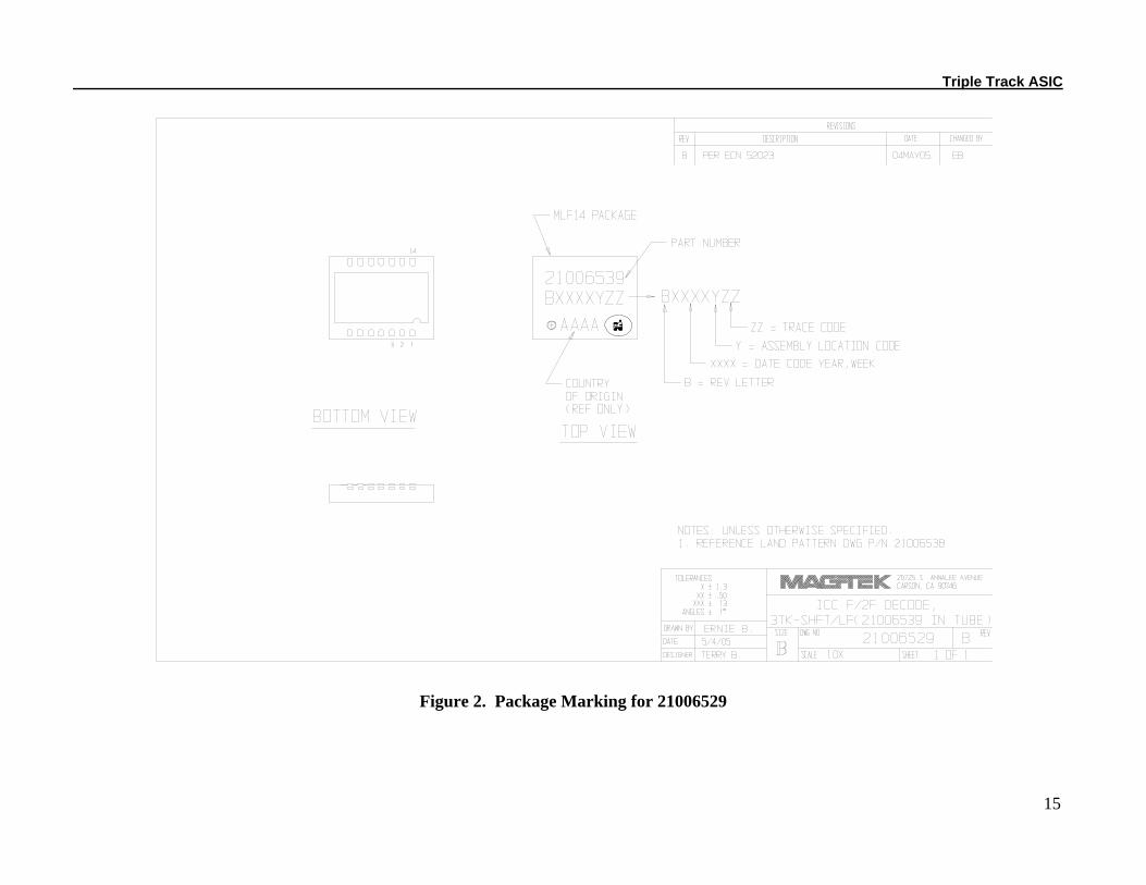
Note that AVSS must be connected to DVSS, and AVDD must be connected to DVDD. A single 0.1µF decoupling capacitor is required. All pins labeled “GND” are not power connections for the chip (as AVSS and DVSS are), but must be grounded for proper configuration of the device. “NC” indicates “No Connection”. These pins must be left floating for proper operation. Mechanical Drawings The 14 pin 4mm x 5 mm MLFTM (MicroLeadFrameTM) package and package marking drawings are shown in Figures 2 and 3.
Triple Track ASIC
15
Figure 2. Package Marking for 21006529

Triple Track ASIC
16
Figure 3. Package Marking for 21006539
Triple Track ASIC
17
PRINTED CIRCUIT BOARD LAYOUT RECOMMENDATIONS AND SCHEMATICS General Guidelines As with any analog or mixed-signal circuit, PCB layout must be approached with care to achieve optimal results with the Triple Track ASIC.
• The low-level analog head signals must be routed clear of any noise sources or digital signals. Use a quiet ground or other low impedance DC source to shield if necessary.
• The loop formed by each head signal conductor and its return path must be minimized to reduce noise pickup. Each track’s pair of conductors must be routed with minimal clearance between them.
• The chip should be decoupled with a 0.1µF ceramic capacitor placed as close as possible to the DVDD and DVSS pins with minimal inductance between the capacitor and the chip.
• DO NOT add additional head loading (resistance or capacitance) to the circuit. Head loading for this chip is dynamic and built into the chip. Additional head loading may degrade performance.
• Unused HEAD_A/B/C pins must not be connected to any potential. IntelliHead The Triple Track ASIC is also available integrated into a magnetic head. As an alternative to a separate ASIC and magnetic head, the Shift-Out IntelliHead product can be easily accommodated on the PCB with very little if any additional board area. Shown in each of the recommended PCB layouts for the Triple Track ASIC is a “hook” for the Shift-Out IntelliHead in the form of a 5-pin connector. If using the Shift-Out IntelliHead, the only component that need be installed on the board is this 5 pin connector. If not using the Shift-Out IntelliHead, the 7-pin connector2 along with all the other components is installed instead of the 5 pin connector. The 7 pin and 5 pin connectors are mutually exclusive in terms of installation. MagTek recommends that this “hook” be included in all Triple Track ASIC PCB layouts so that the customer may have the option of using the Shift-Out IntelliHead with its performance benefits and possible future cost reduction benefits. A note concerning Shift-Out IntelliHead compatibility: The on-chip memory tracks of the Shift-Out IntelliHead are permanently assigned to particular tracks of the magnetic head via internal wires connecting the head coil wires to particular inputs of the built-in ASIC. Typically the dual-track Shift-Out IntelliHead serves as a track 1&2 reader. As such, tracks ‘A’ and ‘B’ of the ASIC correspond to tracks ‘1’ and ‘2’ of the reader respectively when the Shift-Out IntelliHead on a spring is mounted as designed, with the centerline of the spring mounting holes running through the center of track 2. For the less common track 2&3 reader, this Shift-Out IntelliHead/spring assembly may be used in an inverted configuration on the same chassis used by a track 1&2 reader. In this case, on-chip memory track ‘A’ corresponds to physical magnetic stripe track 3, and on-chip memory track ‘B’ corresponds to physical magnetic stripe track 2. This is important since it affects the arrangement of the data upon extraction from the chip. For the triple-track Shift-Out IntelliHead, tracks ‘A’, ‘B’, and ‘C’ of the ASIC are assigned to tracks ‘1’, ‘2’, and ‘3’ respectively of the reader. MagTek recommends that these track assignments be
2 Some MagTek head assemblies use different connectors and pin assignments. Be sure to check your particular head assembly.

Triple Track ASIC
18
respected when using the stand-alone chip to allow for easy migration to the Shift-Out IntelliHead products. The 7-pin connector shown in the PCB layout is Molex part number 53048-0710. The 5-pin Shift-Out IntelliHead connector shown in the PCB layout is Molex part number 53048-0510. Other connectors may be used of course, but this 5-pin connector ensures compatibility when using MagTek Shift-Out IntelliHead assemblies that already include the wiring and connector. The MLFTM-14 is a near-chip-scale package, and requires some care for proper assembly. It is recommended, but not required, that the relatively large pad on the bottom of the package be grounded. For details concerning this package visit http://www.amkor.com/Products/all_products/MLF.cfm A recommended PCB land pattern for the MLFTM-14 package is included in this section. MagTek has successfully used this land pattern in our manufacturing process, but cannot guarantee success in any situation, as manufacturing processes do vary. The MLFTM or similar package is also known as the QFN (Quad-Flat-No-lead) package.

Triple Track ASIC
19
MLFTM-14 with Provision for Shift-Out IntelliHeadTM
Figure 4. PCB Layout

Triple Track ASIC
20
TK-A
TK-C
STROBEDATA*
1234567
J1
7PIN
VDD
HD-CMN1
AVDD4
AVSS2
HD-A3
HD-B5
NC6
HD-C7
STB8NC9
GND11
DATA10
DVSS12DVDD13GND14
U1
SHIFT OUT ASIC
12345
J2
5PIN
DATA*STROBE VDD
VDD
TK-C
TK-B
TK-AVDDTK-B DATA*
STROBE
C1.1uF
IntelliHEAD conector
* The DATA line should beconnected to an OPEN DRAINOUTPUT/INPUT pin forcompatiblity with futureversions.
TO HOST
INDIVIDUAL HEAD COMMONS (HC) TRACES SHOULDTIGHTLY FOLLOW MATCHING TRACE UNTIL THEYARE CLOSE TO CHIP AND THEN BE JOINED TOGETHER.THIS IS TO REDUCE NOISE.
Note that MagTek head assembly pin assignments do vary. The J1 connectorshown represents only one example of a head assembly. Be sure to checkyour particular head assembly for its connector pin assignment.
HC
Figure 5. Schematic

Triple Track ASIC
21
Recommended PCB Land Pattern for the MLFTM-14 Package
Figure 6. Recommended PCB Land Pattern

Triple Track ASIC
ERRATA Products Affected There is no known errata affecting the 21006529/39 ASIC. The following obsolete versions of the ASIC were affected. They are included here for reference. Triple track ASIC, P/N 21006536/37, Revisions A, B, & C. Details See 99875259-12 for details of the errata affecting the above obsolete parts.
22