Embed Size (px)
Citation preview

Triple-Speed Ethernet MegaCore FunctionUser Guide
Last updated for Altera Complete Design Suite: 14.0101 Innovation DriveSan Jose, CA 95134www.altera.com
UG-010082014.06.30
Subscribe
Send Feedback
Contents
About This MegaCore Function.........................................................................1-1About This MegaCore Function................................................................................................................1-1Device Family Support................................................................................................................................1-1Features.........................................................................................................................................................1-110/100/1000 Ethernet MAC Versus Small MAC.....................................................................................1-2High-Level Block Diagrams........................................................................................................................1-3Example Applications..................................................................................................................................1-5MegaCore Verification................................................................................................................................1-6
Optical Platform...............................................................................................................................1-7Copper Platform...............................................................................................................................1-7
Performance and Resource Utilization.....................................................................................................1-7Release Information...................................................................................................................................1-11
Getting Started with Altera IP Cores..................................................................2-1Introduction to Altera IP Cores.................................................................................................................2-1Installing and Licensing IP Cores..............................................................................................................2-1OpenCore Plus IP Evaluation....................................................................................................................2-2Upgrading Outdated IP Cores...................................................................................................................2-2IP Catalog and Parameter Editor...............................................................................................................2-4
Using the Parameter Editor............................................................................................................2-5Design Walkthrough...................................................................................................................................2-6
Creating a New Quartus II Project................................................................................................2-6Specifying IP Core Parameters and Options................................................................................2-7Generating a Design Example or Simulation Model..................................................................2-7Simulate the System.........................................................................................................................2-8Compiling the Triple-Speed Ethernet MegaCore Function Design.........................................2-8Programming an FPGA Device.....................................................................................................2-8
Generated Files.............................................................................................................................................2-9Design Constraint File No Longer Generated...........................................................................2-10
Parameter Settings..............................................................................................3-1Parameter Settings.......................................................................................................................................3-1Core Configuration......................................................................................................................................3-1
Altera Corporation
Triple-Speed Ethernet MegaCore Function User GuideTOC-2
Ethernet MAC Options...............................................................................................................................3-2FIFO Options................................................................................................................................................3-4Timestamp Options.....................................................................................................................................3-5PCS/Transceiver Options...........................................................................................................................3-5
Functional Description.......................................................................................4-110/100/1000 Ethernet MAC.......................................................................................................................4-1
MAC Architecture...........................................................................................................................4-2MAC Interfaces................................................................................................................................4-3MAC Transmit Datapath................................................................................................................4-4MAC Receive Datapath...................................................................................................................4-7MAC Transmit and Receive Latencies........................................................................................4-11FIFO Buffer Thresholds................................................................................................................4-12Congestion and Flow Control......................................................................................................4-16Magic Packets.................................................................................................................................4-17MAC Local Loopback....................................................................................................................4-18MAC Error Correction Code.......................................................................................................4-19MAC Reset......................................................................................................................................4-19PHY Management (MDIO).........................................................................................................4-20Connecting MAC to External PHYs...........................................................................................4-22
1000BASE-X/SGMII PCS With Optional Embedded PMA................................................................4-241000BASE-X/SGMII PCS Architecture......................................................................................4-25Transmit Operation.......................................................................................................................4-26Receive Operation..........................................................................................................................4-27Transmit and Receive Latencies...................................................................................................4-28SGMII Converter...........................................................................................................................4-28Auto-Negotiation...........................................................................................................................4-29Ten-bit Interface............................................................................................................................4-32PHY Loopback...............................................................................................................................4-33PHY Power-Down.........................................................................................................................4-331000BASE-X/SGMII PCS Reset...................................................................................................4-34
Altera IEEE 1588v2 Feature......................................................................................................................4-35IEEE 1588v2 Supported Configurations.....................................................................................4-35IEEE 1588v2 Features....................................................................................................................4-36IEEE 1588v2 Architecture.............................................................................................................4-37IEEE 1588v2 Transmit Datapath.................................................................................................4-37IEEE 1588v2 Receive Datapath....................................................................................................4-38IEEE 1588v2 Frame Format.........................................................................................................4-38
Altera Corporation
TOC-3Triple-Speed Ethernet MegaCore Function User Guide
Triple-Speed Ethernet with IEEE 1588v2 Design Example................................5-1Software Requirements...............................................................................................................................5-1Triple-Speed Ethernet with IEEE 1588v2 Design Example Components...........................................5-2
Base Addresses..................................................................................................................................5-3Triple-Speed Ethernet MAC with IEEE 1588v2 Design Example Files...............................................5-3Creating a New Triple-Speed Ethernet MAC with IEEE 1588v2 Design............................................5-4Triple-Speed Ethernet with IEEE 1588v2 Testbench .............................................................................5-4
Triple-Speed Ethernet with IEEE 1588v2 Testbench Files.........................................................5-5Triple-Speed Ethernet with IEEE 1588v2 Testbench Simulation Flow....................................5-5Simulating Triple-Speed Ethernet with IEEE 1588v2 Testbench with ModelSim
Simulator.....................................................................................................................................5-6
Configuration Register Space.............................................................................6-1MAC Configuration Register Space..........................................................................................................6-1
Base Configuration Registers (Dword Offset 0x00 – 0x17).......................................................6-3Statistics Counters (Dword Offset 0x18 – 0x38).......................................................................6-11Transmit and Receive Command Registers (Dword Offset 0x3A – 0x3B)............................6-13Supplementary Address (Dword Offset 0xC0 – 0xC7)............................................................6-15IEEE 1588v2 Feature (Dword Offset 0xD0 – 0xD6).................................................................6-16IEEE 1588v2 Feature PMA Delay................................................................................................6-17
PCS Configuration Register Space..........................................................................................................6-18Control Register (Word Offset 0x00)..........................................................................................6-20Status Register (Word Offset 0x01).............................................................................................6-22Dev_Ability and Partner_Ability Registers (Word Offset 0x04 – 0x05)................................6-23An_Expansion Register (Word Offset 0x06).............................................................................6-26If_Mode Register (Word Offset 0x14)........................................................................................6-26
Register Initialization................................................................................................................................6-27Triple-Speed Ethernet System with MII/GMII or RGMII.......................................................6-28Triple-Speed Ethernet System with SGMII................................................................................6-30Triple-Speed Ethernet System with 1000BASE-X Interface....................................................6-31
Interface Signals..................................................................................................7-1Interface Signals...........................................................................................................................................7-1
10/100/1000 Ethernet MAC Signals..............................................................................................7-210/100/1000 Multiport Ethernet MAC Signals..........................................................................7-1210/100/1000 Ethernet MAC with 1000BASE-X/SGMII PCS Signals.....................................7-16
Altera Corporation
Triple-Speed Ethernet MegaCore Function User GuideTOC-4
10/100/1000 Multiport Ethernet MAC with 1000BASE-X/SGMII PCS Signals...................7-2010/100/1000 Ethernet MAC with 1000BASE-X/SGMII PCS and Embedded PMA
Signals........................................................................................................................................7-2210/100/1000 Multiport Ethernet MAC with 1000BASE-X/SGMII PCS and Embedded
PMA...........................................................................................................................................7-251000BASE-X/SGMII PCS Signals................................................................................................7-341000BASE-X/SGMII PCS and PMA Signals..............................................................................7-38
Timing.........................................................................................................................................................7-39Avalon-ST Receive Interface........................................................................................................7-39Avalon-ST Transmit Interface.....................................................................................................7-41GMII Transmit...............................................................................................................................7-41GMII Receive..................................................................................................................................7-41RGMII Transmit............................................................................................................................7-42RGMII Receive...............................................................................................................................7-42MII Transmit..................................................................................................................................7-43MII Receive.....................................................................................................................................7-43IEEE 1588v2 Timestamp...............................................................................................................7-43
Design Considerations........................................................................................8-1Optimizing Clock Resources in Multiport MAC with PCS and Embedded PMA.............................8-1
MAC and PCS With GX Transceivers..........................................................................................8-2MAC and PCS With LVDS Soft-CDR I/O...................................................................................8-4
Sharing PLLs in Devices with LVDS Soft-CDR I/O................................................................................8-6Sharing PLLs in Devices with GIGE PHY................................................................................................8-6Sharing Transceiver Quads.........................................................................................................................8-7Migrating From Old to New User Interface For Existing Designs.......................................................8-7
Exposed Ports in the New User Interface.....................................................................................8-7
Timing Constraints.............................................................................................9-1Creating Clock Constraints........................................................................................................................9-1Recommended Clock Frequency...............................................................................................................9-3
Testbench...........................................................................................................10-1Triple-Speed Ethernet Testbench Architecture ....................................................................................10-1Testbench Components............................................................................................................................10-1Testbench Verification..............................................................................................................................10-2Testbench Configuration..........................................................................................................................10-3
Altera Corporation
TOC-5Triple-Speed Ethernet MegaCore Function User Guide
Test Flow.....................................................................................................................................................10-3Simulation Model......................................................................................................................................10-4
Generate the Simulation Model...................................................................................................10-4Simulate the IP Core......................................................................................................................10-4Simulation Model Files.................................................................................................................10-5
Software Programming Interface.....................................................................11-1Driver Architecture...................................................................................................................................11-1Directory Structure....................................................................................................................................11-2PHY Definition .........................................................................................................................................11-2Using Multiple SG-DMA Descriptors....................................................................................................11-4Using Jumbo Frames.................................................................................................................................11-4API Functions.............................................................................................................................................11-5
alt_tse_mac_get_common_speed().............................................................................................11-5alt_tse_mac_set_common_speed().............................................................................................11-5alt_tse_phy_add_profile()............................................................................................................11-6alt_tse_system_add_sys().............................................................................................................11-6triple_speed_ethernet_init().........................................................................................................11-7tse_mac_close()..............................................................................................................................11-7tse_mac_raw_send()......................................................................................................................11-8tse_mac_setGMII mode().............................................................................................................11-9tse_mac_setMIImode().................................................................................................................11-9tse_mac_SwReset()........................................................................................................................11-9
Constants..................................................................................................................................................11-10
Ethernet Frame Format......................................................................................A-1Basic Frame Format....................................................................................................................................A-1VLAN and Stacked VLAN Frame Format..............................................................................................A-1Pause Frame Format...................................................................................................................................A-3
Pause Frame Generation................................................................................................................A-3
Simulation Parameters.......................................................................................B-1Functionality Configuration Parameters.................................................................................................B-1Test Configuration Parameters.................................................................................................................B-3
Time-of-Day (ToD) Clock..................................................................................C-1ToD Clock Features....................................................................................................................................C-1
Altera Corporation
Triple-Speed Ethernet MegaCore Function User GuideTOC-6
ToD Clock Device Family Support...........................................................................................................C-1ToD Clock Performance and Resource Utilization................................................................................C-1ToD Clock Parameter Setting....................................................................................................................C-2ToD Clock Interface Signals......................................................................................................................C-3
ToD Clock Avalon-MM Control Interface Signals....................................................................C-3ToD Clock Avalon-ST Transmit Interface Signals.....................................................................C-4
ToD Clock Configuration Register Space................................................................................................C-5Adjusting ToD Clock Drift............................................................................................................C-6
ToD Synchronizer..............................................................................................D-1ToD Synchronizer Block............................................................................................................................D-2ToD Synchronizer Parameter Settings.....................................................................................................D-3ToD Synchronizer Signals.........................................................................................................................D-4
ToD Synchronizer Common Clock and Reset Signals..............................................................D-4ToD Synchronizer Interface Signals.............................................................................................D-4
Packet Classifier..................................................................................................E-1Packet Classifier Block................................................................................................................................E-1Packet Classifier Signals..............................................................................................................................E-2
Packet Classifier Common Clock and Reset Signals..................................................................E-2Packet Classifier Avalon-ST Interface Signals.............................................................................E-2Packet Classifier Ingress Control Signals.....................................................................................E-3Packet Classifier Control Insert Signals........................................................................................E-4Packet Classifier Timestamp Field Location Signals..................................................................E-5
Additional Information......................................................................................F-1Document Revision History.......................................................................................................................F-2How to Contact Altera................................................................................................................................F-7
Altera Corporation
TOC-7Triple-Speed Ethernet MegaCore Function User Guide

1About This MegaCore Function
2014.06.30
UG-01008 Subscribe Send Feedback
About This MegaCore FunctionThe Altera® Triple-Speed Ethernet MegaCore® function is a configurable intellectual property (IP) corethat complies with the IEEE 802.3 standard. The IP corewas tested and successfully validated by theUniversityof New Hampshire (UNH) interoperability lab. It combines the features of a 10/100/1000-Mbps Ethernetmedia access controller (MAC) and 1000BASE-X/SGMII physical coding sublayer (PCS) with an optionalphysical medium attachment (PMA).
Device Family Support
For new additions and enhancements to the latest Quartus II software and Altera IP, refer to the What’sNew for Altera IP page of the Altera website.
For a list of IP support for all device families, refer to theAll Intellectual Property page of theAltera website.
Features• Complete triple-speed Ethernet IP: 10/100/1000-Mbps Ethernet MAC, 1000BASE-X/SGMII PCS, and
embedded PMA.• Successful validation from the University of New Hampshire (UNH) InterOperability Lab.• 10/100/1000-Mbps Ethernet MAC features:
• Multiple variations: 10/100/1000-Mbps Ethernet MAC in full duplex, 10/100-Mbps Ethernet MACin half duplex, 10/100-Mbps or 1000-Mbps small MAC (resource-efficient variant), and multiportMAC that supports up to 24 ports.
• Support for basic, VLAN, stacked VLAN, and jumbo Ethernet frames. Also supports control framesincluding pause frames.
• Optional internal FIFO buffers, depth from 64 bytes to 256 Kbytes.• Optional statistics counters.
ISO9001:2008Registered
© 2014 Altera Corporation. All rights reserved. ALTERA, ARRIA, CYCLONE, ENPIRION, MAX, MEGACORE, NIOS, QUARTUS and STRATIX wordsand logos are trademarks of Altera Corporation and registered in the U.S. Patent and Trademark Office and in other countries. All otherwords and logos identified as trademarks or service marks are the property of their respective holders as described atwww.altera.com/common/legal.html. Altera warrants performance of its semiconductor products to current specifications in accordance withAltera's standard warranty, but reserves the right to make changes to any products and services at any time without notice. Altera assumesno responsibility or liability arising out of the application or use of any information, product, or service described herein except as expresslyagreed to in writing by Altera. Altera customers are advised to obtain the latest version of device specifications before relying on any publishedinformation and before placing orders for products or services.
www.altera.com
101 Innovation Drive, San Jose, CA 95134
• 1000BASE-X/SGMII PCS features:
• Compliance with Clause 36 of the IEEE standard 802.3.• Optional embedded PMA implemented with serial transceiver or LVDS I/O and soft CDR in Altera
devices that support this interface at 1.25-Gbps data rate.• Support for auto-negotiation as defined in Clause 37.• Support for connection to 1000BASE-X PHYs. Support for 10BASE-T, 100BASE-T, and 1000BASE-
T PHYs if the PHYs support SGMII.
• MAC interfaces:
• Client side—8-bit or 32-bit Avalon® Streaming (Avalon-ST)• Network side—medium independent interface (MII), gigabit medium independent interface (GMII),
or reduced gigabit medium independent interface (RGMII) on the network side. Optional loopbackon these interfaces.
• Optional management data I/O (MDIO) master interface for PHY device management.
• PCS interfaces:
• Client side—MII or GMII• Network side—ten-bit interface (TBI) for PCS without PMA; 1.25-Gbps serial interface for PCS with
PMA implemented with serial transceiver or LVDS I/O and soft CDR in Altera devices that supportthis interface at 1.25-Gbps data rate.
• Programmable features via 32-bit configuration registers:
• FIFO buffer thresholds.• Pause quanta for flow control.• Source and destination MAC addresses.• Address filtering on receive, up to 5 unicast and 64 multicast MAC addresses.• Promiscuous mode—receive frame filtering is disabled in this mode.• Frame length—in MAC only variation, up to 64 Kbytes including jumbo frames. In all variants
containing 1000BASE-X/SGMII PCS, the frame length is up to 10 Kbytes.• Optional auto-negotiation for the 1000BASE-X/SGMII PCS.
• Error correction code protection feature for internal memory blocks.• Optional IEEE 1588v2 feature for 10/100/1000-Mbps Ethernet MAC with SGMII PCS and embedded
serial PMA variation operating without internal FIFO buffer in full-duplex mode, 10/100/1000-MbpsMAC with SGMII PCS and embedded LVDS I/O, or MAC only variation operating without internalFIFO buffer in full-duplex mode. These features are supported in Arria V, Arria 10, Cyclone V, MAX10, and Stratix V device families.
10/100/1000 Ethernet MAC Versus Small MAC
Table 1-1: Feature Comparison between 10/100/1000 Ethernet MAC and Small MAC
Small MAC10/100/1000 Ethernet MACFeature
10/100 Mbps or 1000 MbpsTriple speed (10/100/1000Mbps)Speed
MII only for 10/100 Mbps small MAC, GMII or RGMIIfor 1000 Mbps small MAC
MII/GMII or RGMIIExternalinterfaces
About This MegaCore FunctionAltera Corporation
Send Feedback
UG-0100810/100/1000 Ethernet MAC Versus Small MAC1-2 2014.06.30

Small MAC10/100/1000 Ethernet MACFeature
Limited programmable options. The following optionsare fixed:
• Maximum frame length is fixed to 1518. Jumboframes are not supported.
• FIFO buffer thresholds are set to fixed values.• Store and forward option is not available.• Interpacket gap is set to 12.• Flow control is not supported; pause quanta is not in
use.• Checking of payload length is disabled.• Supplementary MAC addresses are disabled.• Padding removal is disabled.• Sleep mode and magic packet detection is not
supported.
Fully programmableControlinterfaceregisters
Limited configurable options. The following options areNOT available:
• Flow control• VLAN• Statistics counters• Multicast hash table• Loopback• TBI and 1.25 Gbps serial interface• 8-bit wide FIFO buffers
Fully configurableSynthesisoptions
High-Level Block DiagramsHigh-level block diagrams of different variations of the Triple-Speed Ethernet MegaCore function.
Figure 1-1: 10/100/1000-Mbps Ethernet MAC
10/100/1000-MbpsEthernet MAC
MII/GMII/RGMII
Clien
tSide
Netw
orkS
ide
Avalon-ST(Transmit and Receive)
Avalon-MM(Management and Control)
Altera CorporationAbout This MegaCore Function
Send Feedback
1-3High-Level Block DiagramsUG-010082014.06.30
Figure 1-2: Multi-port MAC
10/100/1000-MbpsEthernet MAC
MII/GMII/RGMII
Clien
tSide
Netw
orkS
ide
Avalon-ST(Transmit and Receive)
Avalon-MM(Management and Control)
10/100/1000-MbpsEthernet MAC
MII/GMII/RGMIIAvalon-ST(Transmit and Receive)
Multi-Port MAC
Figure 1-3: 10/100/1000-Ethernet MAC and 1000BASE-X/SGMII PCS with Optional PMA
10/100/1000-MbpsEthernet MAC
MII/GMII
Clien
tSide
Netw
orkS
ide
Avalon-ST(Transmit and
Receive)
Avalon-MM(Management
and Control) 1.25-GbpsSerial
MAC and PCS with Optional Embedded PMA
1000BASE-X/SGMIIPCS
PMA(Optional)
TBI
Figure 1-4: 1000BASE-X/SGMII PCS with Optional PMA
MII/GMII
Clien
tSide
Netw
orkS
ide
1.25-GbpsSerial
PCS with Optional Embedded PMA
1000BASE-X/SGMIIPCS
PMA(Optional)
TBI
About This MegaCore FunctionAltera Corporation
Send Feedback
UG-01008High-Level Block Diagrams1-4 2014.06.30

Figure 1-5: Stand-Alone 10/100/1000 Mbps Ethernet MAC
Gigabit or FastEthernet PHY
DeviceUser
Application
Host Interface MDIO Master
Altera Device Triple-Speed Ethernet MegaCore Function
ManagementApplication
MDI
O
Copper
MII/
GMII/
RGMII
Avalo
n-ST
Avalo
n-MM
10/100/1000-MbpsEthernet MAC
Example ApplicationsThis section shows example applications of different variations of the Triple-Speed Ethernet MegaCorefunction.
The 10/100/1000-Gbps Ethernet MAC only variation can serve as a bridge between the user application andstandard fast or gigabit Ethernet PHY devices.
Figure 1-6: Stand-Alone 10/100/1000 Mbps Ethernet MAC
Example application using this variation for a copper network.
Gigabit or FastEthernet PHY
DeviceUser
Application
Host Interface MDIO Master
Altera Device Triple-Speed Ethernet MegaCore Function
ManagementApplication
MDI
O
Copper
MII/
GMII/
RGMII
Avalo
n-ST
Avalo
n-MM
10/100/1000-MbpsEthernet MAC
When configured to include the 1000BASE-X/SGMII PCS function, the MegaCore function can seamlesslyconnect to any industry standard gigabit Ethernet PHY device via a TBI. Alternatively, when the 1000BASE-X/SGMII PCS function is configured to include an embedded PMA, the MegaCore function can connect
Altera CorporationAbout This MegaCore Function
Send Feedback
1-5Example ApplicationsUG-010082014.06.30

directly to a gigabit interface converter (GBIC), small form-factor pluggable (SFP) module, or an SGMIIPHY.
Figure 1-7: 10/100/1000 Mbps Ethernet MAC and 1000BASE-X PCS with Embedded PMA
Example application using the Triple-Speed Ethernet MegaCore function with 1000BASE-X and PMA. ThePMA block connects to an off-the-shelf GBIC or SFP module to communicate directly over the optical link.
GMIIPMA
FiberGBIC/SFPModule
1.25GbpsSerial
Altera Device
Triple-Speed Ethernet MegaCore Function
TBI10/100/1000-MbpsEthernet MAC
1000BASE-XPCS
Figure 1-8: 10/100/1000 Mbps Ethernet MAC and SGMII PCS with Embedded PMA—GMII/MII to 1.25-GbpsSerial Bridge Mode
Example application using the Triple-Speed Ethernet MegaCore function with 1000BASE-X and PMA, inwhich the PCS function is configured to operate in SGMII mode and acts as a GMII-to-SGMII bridge. Inthis case, the transceiver I/O connects to an off-the-shelf Ethernet PHY that supports SGMII (10BASE-T,100BASE-T, or 1000BASE-T Ethernet PHY).
CopperMII/GMIISGMII PCS PMA 10/100/1000
1.25GbpsSGMII
Altera Device
TBI
Triple-Speed Ethernet MegaCore Function
BASE-T PHY10/100/1000-Mbps
Ethernet MAC
MegaCore VerificationFor each release, Altera verifies the Triple-Speed Ethernet MegaCore function through extensive simulationand internal hardware verification in various Altera device families. The University of New Hampshire(UNH) InterOperability Lab also successfully verified the MegaCore function prior to its release.
Altera used a highly parameterizeable transaction-based testbench to test the following aspects of theMegaCore function:
• Register access
About This MegaCore FunctionAltera Corporation
Send Feedback
UG-01008MegaCore Verification1-6 2014.06.30
• MDIO access• Frame transmission and error handling• Frame reception and error handling• Ethernet frame MAC address filtering• Flow control• Retransmission in half-duplex
Altera has also validated the Triple-Speed EthernetMegaCore function in both optical and copper platformsusing the following development kits:
• Altera Nios II Development Kit, Cyclone II Edition (2C35)• Altera Stratix III FPGA Development Kit• Altera Stratix IV FPGA Development Kit• Quad 10/100/1000 Marvell PHY• MorethanIP 10/100 and 10/100/1000 Ethernet PHY Daughtercards
Optical PlatformIn the optical platform, the 10/100/1000Mbps EthernetMAC, 1000BASE-X/SGMII PCS, and PMA functionsare instantiated.
The FPGA application implements the Ethernet MAC, the 1000BASE-X PCS, and an internal system usingEthernet connectivity. This internal system retrieves all frames received by the MAC function and returnsthem to the sender by manipulating the MAC address fields, thus implementing a loopback. A directconnection to an optical module is provided through an external SFP optical module. Certified 1.25 GBaudoptical SFP transceivers are Finisar 1000BASE-SX FTLF8519P2BNL, Finisar 1000BASE-LX FTRJ-1319-3,and Avago Technologies AFBR-5710Z.
Copper PlatformIn the copper platform, Altera tested the Triple-Speed Ethernet MegaCore function with an external1000BASE-T PHY devices. The MegaCore function is connected to the external PHY device using MII,GMII, RGMII, and SGMII, in conjunction with the 1000BASE-X/SGMII PCS and PMA functions.
A 10/100/1000 Mbps Ethernet MAC and an internal system are implemented in the FPGA. The internalsystem retrieves all frames received by the MAC function and returns them to the sender by manipulatingthe MAC address fields, thus implementing a loopback. A direct connection to an Ethernet link is providedthrough a combined MII to an external PHY module. Certified 1.25 GBaud copper SFP transceivers areFinisar FCMJ-8521-3, Methode DM7041, and Avago Technologies ABCU-5700RZ.
Performance and Resource UtilizationIn the following tables, the fMAX of the configurations is more than 125 MHz.
Altera CorporationAbout This MegaCore Function
Send Feedback
1-7Optical PlatformUG-010082014.06.30

Table 1-2: Arria II GX Performance and Resource Utilization
The estimated resource utilization and performance of the Triple-Speed Ethernet MegaCore function for the ArriaII GX device family. The estimates are obtained by compiling the Triple-Speed Ethernet MegaCore function usingthe Quartus II software targeting an Arria II GX (EP2AGX260EF29I3) device with speed grade -3.
Memory
(M9K Blocks/M144K Blocks/
MLAB Bits)
LogicRegisters
Combina-tionalALUTs
FIFO BufferSize (Bits)
SettingsMegaCore Function
26/0/1828394733572048x32RGMII
All MAC options enabled
Full and half-duplex modessupported
10/100/1000-MbpsEthernet MAC
32/0/146242229220201—MII/GMII All MAC optionsenabled
Full and half-duplex modessupported
8-port 10/100/1000-Mbps EthernetMAC
0/0/0661624—1000BASE-X1000BASE-X/SGMII PCS 1/0/16012141191—1000BASE-X SGMII bridge
enabled PMA block (GXB)
Table 1-3: Stratix IV Performance and Resource Utilization
The estimated resource utilization and performance of the Triple-Speed Ethernet MegaCore function for the StratixIV device family. The estimates are obtained by compiling the Triple-Speed Ethernet MegaCore function using theQuartus II software targeting a Stratix IV GX (EP4SGX530NF45C4) device with speed grade -4.
Memory
(M9K Blocks/ M144KBlocks/MLAB Bits)
LogicRegisters
Combina-tional ALUTs
FIFO BufferSize (Bits)
SettingsMegaCoreFunction
12/1/1408212714102048x32MII
Full and half-duplex modessupported
10/100-Mbps SmallMAC
12/1/128189411572048x32MII All MAC options enabled
12/1/176182711602048x32GMII All MAC options enabled1000-MbpsSmall MAC 12/1/176186111702048x32RGMII All MAC options enabled
About This MegaCore FunctionAltera Corporation
Send Feedback
UG-01008Performance and Resource Utilization1-8 2014.06.30
Memory
(M9K Blocks/ M144KBlocks/MLAB Bits)
LogicRegisters
Combina-tional ALUTs
FIFO BufferSize (Bits)
SettingsMegaCoreFunction
0/0/336433952721—MII/GMII Full and half-duplexmodes supported10/100/
1000-MbpsEthernetMAC
8/0/3620397732012048x8
12/1/3364442533452048x32
12/1/2084399431252048x32MII/GMII All MAC optionsenabled
12/1/2084402131332048x32RGMII All MAC options enabled
0/0/250083437227215—
MII/GMII All MAC optionsenabled
12-port 10/100/1000-MbpsEthernetMAC
0/0/500166840454123—24-port 10/100/1000-MbpsEthernetMAC
0/0/0661624—1000BASE-X
1000BASE-X/SGMIIPCS
2/0/0986808—1000BASE-X SGMII bridgeenabled
2/0/01057819—1000BASE-X SGMII bridgeenabled PMA block (LVDS_IO)
1/0/16012121189—1000BASE-X SGMII bridgeenabled PMA block (GXB)
14/1/2084495039712048×32All MAC options enabled SGMIIbridge enabled
10/100/1000-MbpsEthernetMAC and1000BASE-X/SGMIIPCS
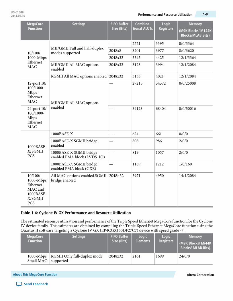
Table 1-4: Cyclone IV GX Performance and Resource Utilization
The estimated resource utilization and performance of the Triple Speed EthernetMegaCore function for theCycloneIV device family. The estimates are obtained by compiling the Triple-Speed Ethernet MegaCore function using theQuartus II software targeting a Cyclone IV GX (EP4CGX150DF27C7) device with speed grade -7.
Memory
(M9K Blocks/ Mi44KBlocks/ MLAB Bits)
LogicRegisters
LogicElements
FIFO BufferSize (Bits)
SettingsMegaCoreFunction
24/0/0169921612048x32RGMII Only full-duplex modesupported
1000-MbpsSmall MAC
Altera CorporationAbout This MegaCore Function
Send Feedback
1-9Performance and Resource UtilizationUG-010082014.06.30

Memory
(M9K Blocks/ Mi44KBlocks/ MLAB Bits)
LogicRegisters
LogicElements
FIFO BufferSize (Bits)
SettingsMegaCoreFunction
31/0/0366656142048x32MII/GMII Full and half-duplexmodes supported
10/100/1000-MbpsEthernetMAC
36/0/01061217017—MII/GMII All MAC optionsenabled
Full and half-duplex modessupported
4-port 10/100/ 1000-MbpsEthernetMAC
0/0/06611149—1000BASE-X1000BASE-X/SGMIIPCS
2/0/011272001—1000BASE-X SGMII bridgeenabled PMA block (GXB)
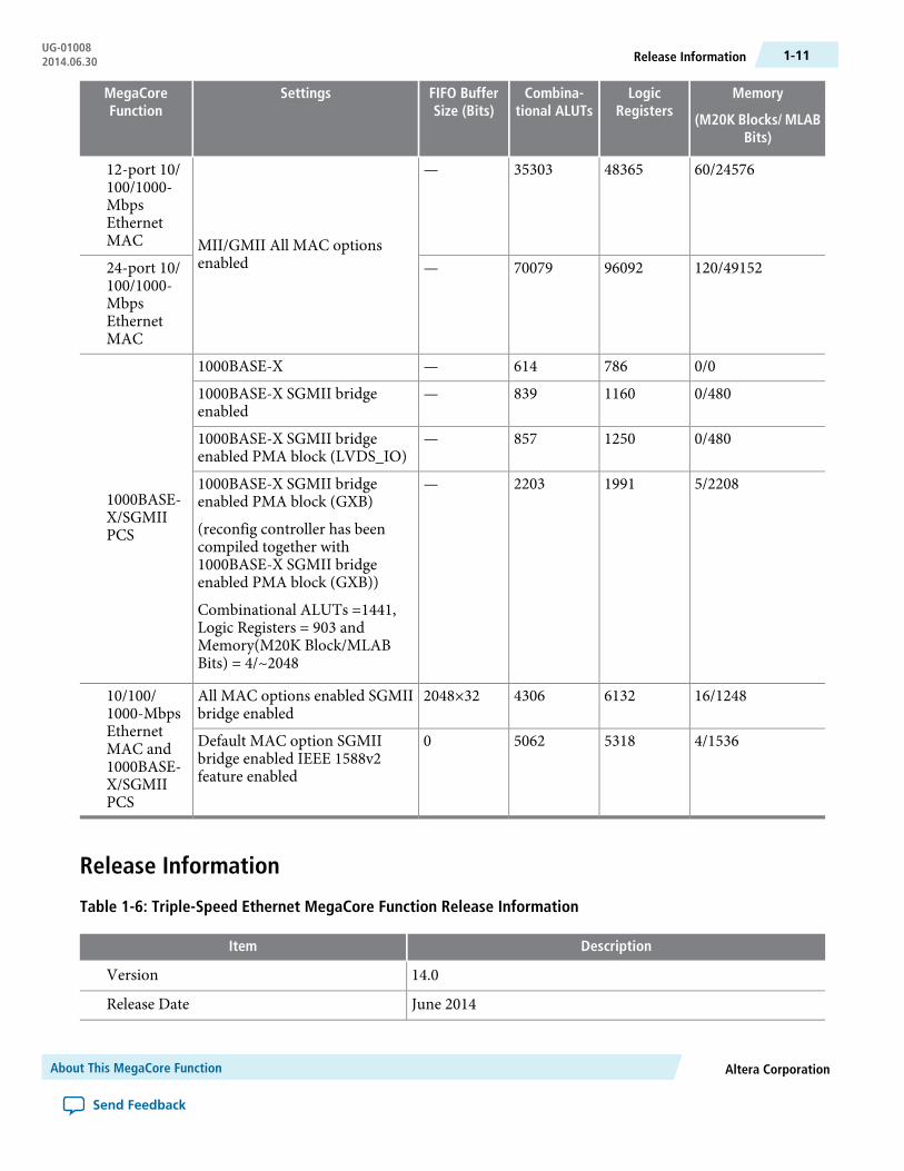
Table 1-5: Stratix V Performance and Resource Utilization
The estimated resource utilization and performance of the Triple-Speed EthernetMegaCore function for the Stratix Vdevice family. The estimates are obtained by compiling the Triple-Speed Ethernet MegaCore function using theQuartus II software targeting a Stratix V GX (5SGXMA7N3F45C3) device with speed grade -3.
Memory
(M20K Blocks/ MLABBits)
LogicRegisters
Combina-tional ALUTs
FIFO BufferSize (Bits)
SettingsMegaCoreFunction
11/0201812612048x32MII
Full and half-duplex modessupported
10/100-Mbps SmallMAC
11/0201812612048x32MII All MAC options enabled
10/128195912272048x32GMII All MAC options enabled1000-MbpsSmall MAC 10/128198412372048x32RGMII All MAC options enabled
5/204842983137—MII/GMII Full and half-duplexmodes supported10/100/
1000-MbpsEthernetMAC
10/2048497136272048x8
16/2048514537772048x32
16/768492834542048x32MII/GMII All MAC optionsenabled
16/768493334662048x32RGMII All MAC options enabled
About This MegaCore FunctionAltera Corporation
Send Feedback
UG-01008Performance and Resource Utilization1-10 2014.06.30
Memory
(M20K Blocks/ MLABBits)
LogicRegisters
Combina-tional ALUTs
FIFO BufferSize (Bits)
SettingsMegaCoreFunction
60/245764836535303—
MII/GMII All MAC optionsenabled
12-port 10/100/1000-MbpsEthernetMAC
120/491529609270079—24-port 10/100/1000-MbpsEthernetMAC
0/0786614—1000BASE-X
1000BASE-X/SGMIIPCS
0/4801160839—1000BASE-X SGMII bridgeenabled
0/4801250857—1000BASE-X SGMII bridgeenabled PMA block (LVDS_IO)
5/220819912203—1000BASE-X SGMII bridgeenabled PMA block (GXB)
(reconfig controller has beencompiled together with1000BASE-X SGMII bridgeenabled PMA block (GXB))
Combinational ALUTs =1441,Logic Registers = 903 andMemory(M20K Block/MLABBits) = 4/~2048
16/1248613243062048×32All MAC options enabled SGMIIbridge enabled
10/100/1000-MbpsEthernetMAC and1000BASE-X/SGMIIPCS
4/1536531850620Default MAC option SGMIIbridge enabled IEEE 1588v2feature enabled
Release Information
Table 1-6: Triple-Speed Ethernet MegaCore Function Release Information
DescriptionItem
14.0Version
June 2014Release Date
Altera CorporationAbout This MegaCore Function
Send Feedback
1-11Release InformationUG-010082014.06.30

DescriptionItem
IP-TRIETHERNETOrdering Code
00BD (Triple-Speed Ethernet MegaCore function)
0104 (IEEE 1588v2)
Product ID(s)
6AF7Vendor ID(s)
Altera verifies that the current version of the Quartus®
II software compiles the previous version of eachMegaCore function. The MegaCore IP Library Release Notes and Errata report any exceptions to thisverification. Altera does not verify compilation with MegaCore function versions older than one release.
Related InformationMegaCore IP Library Release Notes and Errata
About This MegaCore FunctionAltera Corporation
Send Feedback
UG-01008Release Information1-12 2014.06.30
2Getting Started with Altera IP Cores
2014.06.30
UG-01008 Subscribe Send Feedback
Introduction to Altera IP CoresAltera® and strategic IP partners offer a broad portfolio of off-the-shelf, configurable IP cores optimized forAltera devices. Altera delivers an IP core library with the Quartus® II software. OpenCore Plus IP evaluationenables fast acquisition, evaluation, and hardware testing of all Altera IP cores.
Nearly all complex FPGA designs include optimized logic from IP cores. You can integrate optimized andverified IP cores into your design to shorten design cycles and maximize performance. The Quartus IIsoftware includes the Altera IP Library, and supports IP cores from other sources. You can define andgenerate a custom IP variation to represent complex design logic in your project.
The Altera IP Library includes the following IP core types:
• Basic functions• DSP functions• Interface protocols• Memory interfaces and controllers• Processors and peripherals
Related InformationIP User Guide Documentation
Installing and Licensing IP CoresThe Quartus II software includes the Altera IP Library. The library provides many useful IP core functionsfor production use without additional license. You can fully evaluate any licensedAltera IP core in simulationand in hardware until you are satisfied with its functionality and performance. Some Altera IP cores, suchas MegaCore® functions, require that you purchase a separate license for production use. After you purchasea license, visit the Self Service Licensing Center to obtain a license number for any Altera product.
ISO9001:2008Registered
© 2014 Altera Corporation. All rights reserved. ALTERA, ARRIA, CYCLONE, ENPIRION, MAX, MEGACORE, NIOS, QUARTUS and STRATIX wordsand logos are trademarks of Altera Corporation and registered in the U.S. Patent and Trademark Office and in other countries. All otherwords and logos identified as trademarks or service marks are the property of their respective holders as described atwww.altera.com/common/legal.html. Altera warrants performance of its semiconductor products to current specifications in accordance withAltera's standard warranty, but reserves the right to make changes to any products and services at any time without notice. Altera assumesno responsibility or liability arising out of the application or use of any information, product, or service described herein except as expresslyagreed to in writing by Altera. Altera customers are advised to obtain the latest version of device specifications before relying on any publishedinformation and before placing orders for products or services.
www.altera.com
101 Innovation Drive, San Jose, CA 95134

Figure 2-1: IP Core Installation Path
acdsquartus - Contains the Quartus II softwareip - Contains the Altera IP Library and third-party IP cores
altera - Contains the Altera IP Library source code<IP core name> - Contains the IP core source files
The default IP installation directory on Windows is <drive>:\altera\<version number>; on Linux itis <home directory>/altera/ <version number>.
Note:
Related Information
• Altera Licensing Site
• Altera Software Installation and Licensing Manual
OpenCore Plus IP EvaluationAltera's free OpenCore Plus feature allows you to evaluate licensed MegaCore IP cores in simulation andhardware before purchase. You need only purchase a license for MegaCore IP cores if you decide to takeyour design to production. OpenCore Plus supports the following evaluations:
• Simulate the behavior of a licensed IP core in your system.• Verify the functionality, size, and speed of the IP core quickly and easily.• Generate time-limited device programming files for designs that include IP cores.• Program a device with your IP core and verify your design in hardware
OpenCore Plus evaluation supports the following two operation modes:
• Untethered—run the design containing the licensed IP for a limited time.• Tethered—run the design containing the licensed IP for a longer time or indefinitely. This requires a
connection between your board and the host computer.
All IP cores using OpenCore Plus in a design time out simultaneously when any IP core times out.Note:
Upgrading Outdated IP CoresEach IP core has a release version number that corresponds to its Quartus II software release. When youinclude IP cores from a previous version of the Quartus II software in your project, click Project > UpgradeIP Components to identify and upgrade any outdated IP cores.
TheQuartus II software prompts you to upgrade an IP core when the latest version includes port, parameter,or feature changes. The Quartus II software also notifies you when IP cores are unsupported or cannotupgrade in the current version of the Quartus II software. Most Altera IP cores support automatic simulta-neous upgrade, as indicated in the Upgrade IP Components dialog box. IP cores unsupported by auto-upgrade may require regeneration in the parameter editor, as indicated in the Upgrade IP Componentsdialog box.
Getting Started with Altera IP CoresAltera Corporation
Send Feedback
UG-01008OpenCore Plus IP Evaluation2-2 2014.06.30
Before you begin
Upgrading IP cores changes your original design files. If you have not already preserved your original sourcefiles, click Project > Archive Project and save the project archive.
1. In the latest version of the Quartus II software, open the Quartus II project containing an outdated IPcore variation.
File paths in a restored project archive must be relative to the project directory and you mustreference the IP variation .v or .vhd file or .qsys file, not the .qip file.
Note:
2. ClickProject >Upgrade IPComponents. TheUpgrade IPComponents dialog box displays all outdatedIP cores in your project, along with basic instructions for upgrading each core.
3. To simultaneously upgrade all IP cores that support automatic upgrade, click Perform AutomaticUpgrade. The IP variation upgrades to the latest version.
4. To upgrade IP cores unsupported by automatic upgrade, follow these steps:a. Select the IP core in the Upgrade IP Components dialog box.b. Click Upgrade in Editor. The parameter editor appears.c. ClickFinish orGenerate to regenerate the IP variation and complete the upgrade. The version number
updates when complete.
Example designs provided with any Altera IP core regenerate automatically whenever youupgrade the IP core in the Upgrade IP Components dialog box.
Note:
Figure 2-2: Upgrading Outdated IP Cores
Displays upgradestatus for all IP coresin the Project
Upgrades all IP core that support “Auto Upgrade”Upgrades individual IP cores unsupported by “Auto Upgrade”
Indicates IP upgrade is:RequiredOptionalCompleteUnsupported
Altera CorporationGetting Started with Altera IP Cores
Send Feedback
2-3Upgrading Outdated IP CoresUG-010082014.06.30
Example 2-1: Upgrading IP Cores at the Command Line
Alternatively, you can upgrade IP cores at the command line. To upgrade a single IP core, type thefollowing command:
quartus_sh --ip_upgrade -variation_files <my_ip_path> <project>
To upgrade a list of IP cores, type the following command:
quartus_sh --ip_upgrade -variation_files "<my_ip>.qsys;<my_ip>.<hdl>; <project>"
IP cores older than Quartus II software version 12.0 do not support upgrade. Alteraverifies that the current version of the Quartus II software compiles the previous
Note:
version of each IP core. The MegaCore IP Library Release Notes reports anyverification exceptions forMegaCore IP. TheQuartus II Software andDevice SupportRelease Notes reports any verification exceptions for other IP cores. Altera does notverify compilation for IP cores older than the previous two releases.
Related Information
• MegaCore IP Library Release Notes
• Quartus II Software and Device Support Release Notes
IP Catalog and Parameter EditorTheQuartus II IP Catalog (Tools > IPCatalog) and parameter editor help you easily customize and integrateIP cores into your project. You can use the IP Catalog and parameter editor to select, customize, and generatefiles representing your custom IP variation.
The IP Catalog automatically displays the IP cores available for your target device. Double-click any IP corename to launch the parameter editor and generate files representing your IP variation. The parameter editorprompts you to specify your IP variation name, optional ports, architecture features, and output file generationoptions. The parameter editor generates a top-level .qsys or .qip file representing the IP core in your project.Alternatively, you can define an IP variation without an open Quartus II project. When no project is open,select the Device Family directly in IP Catalog to filter IP cores by device.
The IP Catalog is also available in Qsys (View > IP Catalog). The Qsys IP Catalog includes exclusivesystem interconnect, video and image processing, and other system-level IP that are not available inthe Quartus II IP Catalog.
Note:
Use the following features to help you quickly locate and select an IP core:
• Filter IP Catalog to Show IP for active device family or Show IP for all device families.• Search to locate any full or partial IP core name in IP Catalog. Click Search for Partner IP, to access
partner IP information on the Altera website.• Right-click an IP core name in IPCatalog to display details about supported devices, installation location,
and links to documentation.
Getting Started with Altera IP CoresAltera Corporation
Send Feedback
UG-01008IP Catalog and Parameter Editor2-4 2014.06.30
Figure 2-3: Quartus II IP Catalog
Search and filter IP for your target device
Double-click to customize, right-click for information
The IP Catalog and parameter editor replace the MegaWizard™
Plug-In Manager in the Quartus IIsoftware. The Quartus II software may generate messages that refer to the MegaWizard Plug-In
Note:
Manager. Substitute "IP Catalog and parameter editor" for "MegaWizard Plug-In Manager" in thesemessages.
Using the Parameter EditorThe parameter editor helps you to configure your IP variation ports, parameters, architecture features, andoutput file generation options.
• Use preset settings in the parameter editor (where provided) to instantly apply preset parameter valuesfor specific applications.
• View port and parameter descriptions, and links to documentation.• Generate testbench systems or example designs (where provided).
Altera CorporationGetting Started with Altera IP Cores
Send Feedback
2-5Using the Parameter EditorUG-010082014.06.30

Figure 2-4: IP Parameter Editors
View IP portand parameterdetails
Apply preset parameters forspecific applications
Specify your IP variation nameand target device
Legacy parametereditors
Design WalkthroughThis walkthrough explains how to create a Triple-Speed Ethernet MegaCore function design using Qsys inthe Quartus II software. After you generate a custom variation of the Triple-Speed Ethernet MegaCorefunction, you can incorporate it into your overall project.
This walkthrough includes the following steps:
1. Creating a New Quartus II Project on page 2-62. Specifying IP Core Parameters and Options on page 2-73. Generating a Design Example or Simulation Model on page 2-74. Simulate the System on page 2-85. Compiling the Triple-Speed Ethernet MegaCore Function Design on page 2-86. Programming an FPGA Device on page 2-8
Creating a New Quartus II ProjectYou need to create a new Quartus II project with the New Project Wizard, which specifies the workingdirectory for the project, assigns the project name, and designates the name of the top-level design entity.
To create a new project, follow these steps:
1. From the Windows Start menu, select Programs >Altera >Quartus II <version> to launch the QuartusII software. Alternatively, you can use the Quartus II Web Edition software.
2. On the File menu, click New Project Wizard.3. In the New Project Wizard: Directory, Name, Top-Level Entity page, specify the working directory,
project name, and top-level design entity name. Click Next.
Getting Started with Altera IP CoresAltera Corporation
Send Feedback
UG-01008Design Walkthrough2-6 2014.06.30
4. In the New Project Wizard: Add Files page, select the existing design files (if any) you want to includein the project.(1) Click Next.
5. In the New Project Wizard: Family & Device Settings page, select the device family and specific deviceyou want to target for compilation. Click Next.
6. In the EDA Tool Settings page, select the EDA tools you want to use with the Quartus II software todevelop your project.
7. The last page in the New Project Wizard window shows the summary of your chosen settings. ClickFinish to complete the Quartus II project creation.
Specifying IP Core Parameters and OptionsFollow these steps to specify IP core parameters and options.
1. In the IP Catalog (Tools > IP Catalog), locate and double-click the name of the IP core to customize.The parameter editor appears.
2. Specify a top-level name for your custom IP variation. This name identifies the IP core variation files inyour project. If prompted, also specify the target Altera device family and output file HDL preference.Click OK.
3. Specify parameters and options for your IP variation:
• Optionally select preset parameter values. Presets specify all initial parameter values for specificapplications (where provided).
• Specify parameters defining the IP core functionality, port configurations, and device-specific features.• Specify options for generation of a timing netlist, simulation model, testbench, or example design
(where applicable).• Specify options for processing the IP core files in other EDA tools.
4. Click Finish or Generate to generate synthesis and other optional files matching your IP variationspecifications. The parameter editor generates the top-level .qip or .qsys IP variation file and HDL filesfor synthesis and simulation. Some IP cores also simultaneously generate a testbench or example designfor hardware testing.
5. To generate a simulation testbench, click Generate > Generate Testbench System. Generate TestbenchSystem is not available for some IP cores that do not provide a simulation testbench.
6. To generate a top-level HDL example for hardware verification, click Generate > HDL Example.Generate > HDL Example is not available for some IP cores.
The top-level IP variation is added to the current Quartus II project. Click Project > Add/Remove Files inProject to manually add a .qip or .qsys file to a project. Make appropriate pin assignments to connect ports.
Generating a Design Example or Simulation ModelAfter you have parameterized the MegaCore function, you can also generate a design example, in additionto generating the MegaCore component files.
In the parameter editor, click ExampleDesign to create a functional simulation model (design example thatincludes a testbench). The testbench and the automated script are located in the <variation name>_testbenchdirectory.
(1) To include existing files, you must specify the directory path to where you installed the MegaCore function.Youmust also add the user libraries if you installed theMegaCore IP Library in a different directory fromwhereyou installed the Quartus II software.
Altera CorporationGetting Started with Altera IP Cores
Send Feedback
2-7Specifying IP Core Parameters and OptionsUG-010082014.06.30
Generating a design example can increase processing time.Note:
You can now integrate your custom IP core instance in your design, simulate, and compile.While integratingyour IP core instance into your design, you must make appropriate pin assignments. You can create a virtualpin to avoid making specific pin assignments for top-level signals while you are simulating and not readyto map the design to hardware.
Related Information
• TestbenchMore information about the MegaCore function simulation model.
• Quartus II HelpMore information about the Quartus II software, including virtual pins.
Simulate the SystemDuring system generation, Qsys generates a functional simulation model—or design example that includesa testbench—which you can use to simulate your system in any Altera-supported simulation tool.
Related Information
• Quartus II Software Release NotesMore information about the latest Altera-supported simulation tools.
• Simulating Altera DesignsMore information in volume 3 of the Quartus II Handbook about simulating Altera IP cores.
• System Design with QsysMore information in volume 1 of the Quartus II Handbook about simulating Qsys systems.
Compiling the Triple-Speed Ethernet MegaCore Function Design
Before you begin
Refer toDesignConsiderations on page 8-1 chapter before compiling the Triple-Speed Ethernet MegaCorefunction design.
To compile your design, click Start Compilation on the Processing menu in the Quartus II software. Youcan use the generated .qip file to include relevant files into your project.
Related InformationQuartus II HelpMore information about compilation in Quartus II software.
Programming an FPGA DeviceAfter successfully compiling your design, program the targetedAltera devicewith theQuartus II Programmerand verify the design in hardware. For instructions on programming the FPGA device, refer to the DeviceProgramming section in volume 3 of the Quartus II Handbook.
Related InformationDevice Programming
Getting Started with Altera IP CoresAltera Corporation
Send Feedback
UG-01008Simulate the System2-8 2014.06.30

Generated FilesThe type of files generated in your project directory and their names may vary depending on the customvariation of the MegaCore function you created.
Table 2-1: Generated Files
DescriptionFile Name
A MegaCore function variation file, which defines a VHDL orVerilog HDL top-level description of the custom MegaCorefunction. Instantiate the entity defined by this file inside yourdesign. Include this file when compiling your design in theQuartus II software.
<variation_name>.v or
<variation_name>.vhd
Quartus II symbol file for the MegaCore function variation. Youcan use this file in the Quartus II block diagram editor.
<variation_name>.bsf
Contains Quartus II project information for your MegaCorefunction variations.
<variation_name>.qip and
<variation_name>.sip
A VHDL component declaration file for the MegaCore functionvariation. Add the contents of this file to any VHDL architecturethat instantiates the MegaCore.
<variation_name>.cmp
Simulation Package Descriptor file. Specifies the files requiredfor simulation.
<variation_name>.spd
Testbench Files (in <variation_name>_testbench folder)
Read me file for the testbench design.README.txt
Dummy Quartus II project and project setting file. Use this tostart theQuartus II in the correct directory to launch the generate_sim_verilog.tcl and generate_sim_vhdl.tcl files.
generate_sim.qpf and
generate_sim.qsf
A Tcl script to generate the DUT VHDL or Verilog HDLsimulation model for use in the testbench.
generate_sim_verilog.tcl and
generate_sim_vhdl.tcl
VHDL or Verilog HDL testbench that exercises your MegaCorefunction variation in a third party simulator.
/testbench_vhdl/<variation_name>/<variation_name>_tb.vhd or
/testbench_verilog/<variation_name>/<variation_name>_tb.v
A Tcl script for use with the ModelSim simulation software./testbench_vhdl/<variation_name>/run_<variation_name>_tb.tcl or
/testbench_verilog/<variation_name>/run_ <variation_name>_tb.tcl
A signal tracingmacro script usedwith theModelSim simulationsoftware to display testbench signals.
/testbench_vhdl/<variation_name>/<variation_name>_wave.do or
/testbench_verilog/<variation_name>/<variation_name>_wave.do
Altera CorporationGetting Started with Altera IP Cores
Send Feedback
2-9Generated FilesUG-010082014.06.30

DescriptionFile Name
A directory containing VHDL and Verilog HDL models of theEthernet generators andmonitors used by the generated testbench.
/testbench_vhdl/models or
/testbench_verilog/models
Design Constraint File No Longer GeneratedFor a new Triple-Speed Ethernet MegaCore function created using the Quartus II software ACDS 13.0 orlater, the Quartus II software no longer generate the <variation_name>_constraints.tcl file that contains thenecessary constraints for the compilation of your MegaCore Function variation. Table 2-2 lists therecommended Quartus II pin assignments that you can set in your design.
Table 2-2: Recommended Quartus II Pin Assignments
Design PinDescriptionAssignmentValue
Quartus II PinAssignment
MII, GMII, RGMII, TBI input pins.To optimize I/O timing for MII, GMIIand TBI interface.
ONFAST_INPUT_REGISTER
MII, GMII, RGMII, TBI outputpins.
To optimize I/O timing for MII, GMIIand TBI interface.
ONFAST_OUTPUT_REGISTER
GXB transceiver serial input andoutput pins.
I/O standard for GXB serial input andoutput pins.
1.4-V PCMLor 1.5-VPCML
IO_STANDARD
LVDS/IO transceiver serial inputand output pins.
I/O standard for LVDS/IO serial inputand output pins.
LVDSIO_STANDARD
• ref_clk forMACandPCSwithLVDS/IO (with internal FIFO).
• clk and reset pins for MAConly (without internal FIFO).
• clk and ref_clk input pins forMAC and PCS with transceiver(without internal FIFO).
To assign clock signals to use the globalclock network. Use this setting to guidethe Quartus II in the fitter process forbetter timing closure.
Global clockGLOBAL_SIGNAL
• rx_clk <n> and tx_clk <n>
input pins for MAC only usingMII/GMII interface (withoutinternal FIFO).
• rx_clk <n> input pin for MAConly using RGMII interface(without internal FIFO).
To assign clock signals to use theregional clock network.Use this settingto guide the Quartus II in the fitterprocess for better timing closure.
Regional clockGLOBAL_SIGNAL
Signals for Arria V devices:
• *reset_ff_wr and *reset_ff_rd
• *| altera_tse_reset_
synchronizer_chain_out
To prevent a signal to be used as aglobal signal.
OFFGLOBAL_SIGNAL
Getting Started with Altera IP CoresAltera Corporation
Send Feedback
UG-01008Design Constraint File No Longer Generated2-10 2014.06.30
3Parameter Settings
2014.06.30
UG-01008 Subscribe Send Feedback
Parameter SettingsYou customize theTriple-SpeedEthernetMegaCore function by specifying parameters using theTriple-SpeedEthernet parameter editor, launched fromQsys in theQuartus II software. The customization enables specificcore features during synthesis and generation.
This chapter describes the parameters and how they affect the behavior of the MegaCore function. Eachsection corresponds to a page in the Parameter Settings tab in the parameter editor interface.
Core Configuration
Table 3-1: Core Configuration Parameters
DescriptionValueName
Determines the primary blocks to include in thevariation.
• 10/100/1000 MbEthernet MAC
• 10/100/1000 MbEthernet MAC with1000BASE-X/SGMIIPCS
• 1000BASE-X/SGMIIPCS only
• 1000 Mb Small MAC• 10/100Mb SmallMAC
Core Variation
Turn on this option to enable ECC protectionfor internal memory blocks.
On/OffEnable ECC protection
ISO9001:2008Registered
© 2014 Altera Corporation. All rights reserved. ALTERA, ARRIA, CYCLONE, ENPIRION, MAX, MEGACORE, NIOS, QUARTUS and STRATIX wordsand logos are trademarks of Altera Corporation and registered in the U.S. Patent and Trademark Office and in other countries. All otherwords and logos identified as trademarks or service marks are the property of their respective holders as described atwww.altera.com/common/legal.html. Altera warrants performance of its semiconductor products to current specifications in accordance withAltera's standard warranty, but reserves the right to make changes to any products and services at any time without notice. Altera assumesno responsibility or liability arising out of the application or use of any information, product, or service described herein except as expresslyagreed to in writing by Altera. Altera customers are advised to obtain the latest version of device specifications before relying on any publishedinformation and before placing orders for products or services.
www.altera.com
101 Innovation Drive, San Jose, CA 95134

DescriptionValueName
Determines the Ethernet-side interface of theMAC block.
• MII—The only option available for 10/100Mb Small MAC core variations.
• GMII—Available only for 1000 Mb SmallMAC core variations.
• RGMII—Available for 10/100/1000 MbEthernetMACand1000MbSmallMACcorevariations.
• MII/GMII—Available only for 10/100/1000Mb Ethernet MAC core variations. If this isselected, media independent interface (MII)is used for the 10/100 interface, and gigabitmedia independent interface (GMII) for thegigabit interface.
• MII• GMII• RGMII• MII/GMII
Interface
Turn on this option to include internal FIFObuffers in the core. You can only include internalFIFO buffers in single-port MACs.
On/OffUse internal FIFO
Specifies the number of Ethernet ports supportedby the IP core. This parameter is enabled if theparameter Use internal FIFO is turned off. Amultiport MAC does not support internal FIFObuffers.
1, 4, 8, 12, 16, 20, and 24Number of ports
This option is only available for variations thatinclude the PCS block.
• None—the PCS block does not include anintegrated transceivermodule. ThePCSblockimplements a ten-bit interface (TBI) to anexternal SERDES chip.
• LVDS I/O orGXB—theMegaCore functionincludes an integrated transceivermodule toimplement a 1.25 Gbps transceiver.RespectiveGXBmodule is included for targetdevices with GX transceivers. For targetdevices with LVDS I/O including Soft-CDRsuch as Stratix III, the ALTLVDS module isincluded.
• None• LVDS I/O• GXB
Transceiver type
Ethernet MAC OptionsThese options are enabledwhen your variation includes theMAC function. In smallMACs, only the followingoptions are available:
Parameter SettingsAltera Corporation
Send Feedback
UG-01008Ethernet MAC Options3-2 2014.06.30
• Enable MAC 10/100 half duplex support (10/100 Small MAC variations)• Align packet headers to 32-bit boundary (10/100 and 1000 Small MAC variations)
Table 3-2: MAC Options Parameters
DescriptionValueName
Ethernet MAC Options
Turn on this option to include support for halfduplex operation on 10/100 Mbps connections.
On/OffEnable MAC 10/100 halfduplex support
Turn on this option to enable local loopback onthe MAC’s MII, GMII, or RGMII interface. Ifyou turn on this option, the loopback functioncan be dynamically enabled or disabled duringsystem operation via the MAC configurationregister.
On/OffEnable local loopback onMII/GMII/RGMII
Turn on this option to include support forsupplementary destination MAC unicastaddresses for fast hardware-based received framefiltering.
On/OffEnable supplemental MACunicast addresses
Turn on this option to include support for simplenetwork monitoring protocol (SNMP)management informationbase (MIB) and remotemonitoring (RMON) statistics counter registersfor incoming and outgoing Ethernet packets.
By default, the width of all statistics counters are32 bits.
On/OffInclude statistics counters
Turn on this option to extend the width ofselected statistics counters— aOctetsTransmit-
tedOK, aOctetsReceivedOK, and etherStat-
sOctets—to 64 bits.
On/OffEnable 64-bit statistics bytecounters
Turn on this option to implement a hash table,a fast hardware-based mechanism to detect andfilter multicast destination MAC address inreceived Ethernet packets.
On/OffInclude multicast hashtable
Turn on this option to include logic that alignsall packet headers to a 32-bit boundary. Thishelps reduce software overhead processing inrealignment of data buffers.
This option is available for MAC variations with32 bits wide internal FIFO buffers and MACvariations without internal FIFO buffers.
You must turn on this option if you intend touse the Triple-Speed Ethernet MegaCorefunction with the Interniche TCP/IP protocolstack.
On/OffAlign packet headers to 32-bitboundary
Altera CorporationParameter Settings
Send Feedback
3-3Ethernet MAC OptionsUG-010082014.06.30

DescriptionValueName
Turn on this option to include the logic for full-duplex flow control that includes pause framesgeneration and termination.
On/OffEnable full-duplex flowcontrol
Turn on this option to include the logic forVLAN and stacked VLAN frame detection.When turned off, the MAC does not detectVLAN and staked VLAN frames. The MACforwards these frames to the user applicationwithout processing them.
On/OffEnable VLAN detection
Turn on this option to include logic for magicpacket detection (Wake-on LAN).
On/OffEnablemagicpacket detection
MDIO Module
Turn on this option if youwant to access externalPHY devices connected to the MAC function.When turned off, the core does not include thelogic or signals associated with the MDIOinterface.
On/OffInclude MDIO module(MDC/MDIO)
Clock divisor to divide the MAC controlinterface clock to produce theMDCclock outputon the MDIO interface. The default value is 40.
For example, if the MAC control interface clockfrequency is 100 MHz and the desired MDCclock frequency is 2.5 MHz, a host clock divisorof 40 should be specified.
Altera recommends that the division factor isdefined such that the MDC frequency does notexceed 2.5 MHz.
—Host clock divisor
FIFO OptionsThe FIFO options are enabled only for MAC variations that include internal FIFO buffers.
Table 3-3: FIFO Options Parameters
ParameterValueName
Width
Determines the data width in bits of the transmitand receive FIFO buffers.
8 Bits and 32 BitsWidth
Depth
Determines the depth of the internal FIFObuffers.Between 64 and 64K
Transmit
Receive
Parameter SettingsAltera Corporation
Send Feedback
UG-01008FIFO Options3-4 2014.06.30
Timestamp Options
Table 3-4: Timestamp Options Parameters
ParameterValueName
Timestamp
Turn on this parameter to enable time stampingon the transmitted and received frames.
On/OffEnable timestamping
Turn on this parameter to insert timestamp onPTP messages for 1-step clock based on the TXTimestamp Insert Control interface.
This parameter is disabled if you do not turn onEnable timestamping.
On/OffEnable PTP 1-step clock
Use this parameter to set the width in bits forthe timestamp fingerprint on the TX path. Thedefault value is 4 bits.
—Timestamp fingerprintwidth
PCS/Transceiver OptionsThe PCS/Transceiver options are enabled only if your core variation includes the PCS function.
Table 3-5: PCS/Transceiver Options Parameters
ParameterValueName
PCS Options
Configures the PHY ID of the PCS block.—PHY ID (32 bit)
Turn on this option to add the SGMII clock andrate-adaptation logic to the PCS block. Thisoption allows you to configure the PCS either inSGMII mode or 1000Base-X mode. If yourapplication only requires 1000BASE-X PCS,turning off this option reduces resource usage.
In Cyclone IV GX devices, REFCLK[0,1] andREFCLK[4,5] cannot connect directly to theGCLK network. If you enable the SGMII bridge,you must connect ref_clk to an alternativededicated clock input pin.
On/OffEnable SGMII bridge
Transceiver Options—apply only to variations that include GXB transceiver blocks
Altera CorporationParameter Settings
Send Feedback
3-5Timestamp OptionsUG-010082014.06.30

ParameterValueName
This option is not supported in Stratix V,Arria V, Arria V GZ, and Cyclone V devices.
Turn on this option to export the powerdownsignal of the GX transceiver to the top-level ofyour design. Powerdown is shared among thetransceivers in a quad. Therefore, turning on thisoption in multiport Ethernet configurationsmaximizes efficient use of transceivers withinthe quad.
Turn off this option to connect the powerdownsignal internally to the PCS control registerinterface. This connection allows the hostprocessor to control the transceiver powerdownin your system.
On/OffExport transceiverpowerdown signal
This option is always turned on in devices otherthan Arria GX and Stratix II GX. When thisoption is turned on, the MegaCore functionincludes the dynamic reconfiguration signals.
For designs targeting devices other thanArria V,Cyclone V, Stratix V, and Arria 10, Alterarecommends that you instantiate the ALTGX_RECONFIG megafunction and connect themegafunction to the dynamic reconfigurationsignals to enable offset cancellation.
For Arria V, Cyclone V, and Stratix V designs,Altera recommends that you instantiate theTransceiver Reconfiguration Controllermegafunction and connect the megafunction tothe dynamic reconfiguration signals to enableoffset cancellation. The transceivers in theArria V, Cyclone V, and Stratix V designs areconfigured with Altera Custom PHY IP core.The Custom PHY IP core require two reconfig-uration interfaces for external reconfigurationcontroller. For more information on thereconfiguration interfaces required, refer to theAltera Transceiver PHY IP Core User Guideand the respective device handbook.
For more information about quad sharingconsiderations, refer to SharingPLLs inDeviceswith GIGE PHY on page 8-6 .
On/OffEnable transceiver dynamicreconfiguration
Parameter SettingsAltera Corporation
Send Feedback
UG-01008PCS/Transceiver Options3-6 2014.06.30

ParameterValueName
Specifies the channel number for the GXBtransceiver block. In a multiport MAC, thisparameter specifies the channel number for thefirst port. Subsequent channel numbers are infour increments.
In designs with multiple instances of GXBtransceiver block (multiple instances of Triple-Speed Ethernet IP core with GXB transceiverblock or a combination of Triple-Speed EthernetIP core and other IP cores), Altera recommendsthat you set a unique starting channel numberfor each instance to eliminate conflicts when theGXB transceiver blocks share a transceiver quad.
This option is not supported inArria V, CycloneV, Stratix V, and Arria 10 devices. For thesedevices, the channel numbers depends on thedynamic reconfiguration controller.
0 – 284Starting channel number
Series V GXB Transceiver Options
This option is only available for variations thatinclude the PCS block for Stratix V and Arria VGZ devices.
Specifies the TX phase-locked loops (PLLs)type—CMU or ATX—in the GXB transceiverfor Series V devices.
• CMU• ATX
TX PLLs type
Turn on this option to enable SyncE support byseparating the TX PLL and RX PLL referenceclock.
On/OffEnable SyncE Support
This option is only available for variations thatinclude the PCS block for Arria V and CycloneV devices.
Specifies the TX PLL clock network type.
• x1• xN
TX PLL clock network
Arria 10 GXB Transceiver Options
Turn on this option for the MegaCore functionto include the dynamic reconfiguration signals.
On/OffEnable Arria 10 transceiverdynamic reconfiguration
You must configure the Arria 10 Transceiver ATX PLL with an output clock frequency of 1250.0MHz (instead of applying the default value of 625 MHz) when using the Arria 10 Transceiver NativePHY with the Triple-Speed Ethernet IP core.
Note:
Refer to the respective device handbook formore information on dynamic reconfiguration inAltera devices.
Related InformationArria 10 Transceiver PHY User GuideMore information about the Arria 10 Transceiver ATX PLL.
Altera CorporationParameter Settings
Send Feedback
3-7PCS/Transceiver OptionsUG-010082014.06.30

4Functional Description
2014.06.30
UG-01008 Subscribe Send Feedback
The Triple-Speed Ethernet MegaCore function includes the following functions:
• 10/100/1000 Ethernet MAC• 1000BASE-X/SGMII PCS With Optional Embedded PMA• Altera IEEE 1588v2
10/100/1000 Ethernet MACThe Altera 10/100/1000 Ethernet MAC function handles the flow of data between user applications andEthernet network through an internal or external Ethernet PHY.Altera offers the followingMACvariations:
• Variations with internal FIFO buffers—supports only single port.• Variations without internal FIFO buffers—supports up to 24 ports and the ports can operate at different
speeds.• Small MAC—provides basic functionalities of a MAC function using minimal resources.
Refer to 10/100/1000 EthernetMACVersus Small MAC on page 1-2 for a feature comparison betweenthe 10/100/1000 Ethernet MAC and small MAC.
The MAC function supports the following Ethernet frames: basic, VLAN and stacked VLAN, jumbo, andcontrol frames. For more information about these frame formats, refer to Ethernet Frame Format on page12-1.
ISO9001:2008Registered
© 2014 Altera Corporation. All rights reserved. ALTERA, ARRIA, CYCLONE, ENPIRION, MAX, MEGACORE, NIOS, QUARTUS and STRATIX wordsand logos are trademarks of Altera Corporation and registered in the U.S. Patent and Trademark Office and in other countries. All otherwords and logos identified as trademarks or service marks are the property of their respective holders as described atwww.altera.com/common/legal.html. Altera warrants performance of its semiconductor products to current specifications in accordance withAltera's standard warranty, but reserves the right to make changes to any products and services at any time without notice. Altera assumesno responsibility or liability arising out of the application or use of any information, product, or service described herein except as expresslyagreed to in writing by Altera. Altera customers are advised to obtain the latest version of device specifications before relying on any publishedinformation and before placing orders for products or services.
www.altera.com
101 Innovation Drive, San Jose, CA 95134

MAC ArchitectureFigure 4-1: 10/100/1000 Ethernet MAC With Internal FIFO Buffers
ReceiveFIFO Buffer
TransmitFIFO Buffer
Configuration andStatistics MDIO Master
CRC CheckPauseFrame
Termination
MII/GMII /RGMIIReceive
LocalLoopbackReceiver Control
MII/GMII /RGMIITransmit
PHYManagementInterface
Control Interface(Avalon -MM)
Magic PacketDetection
Ethernet SideSystem Side
CRCGeneration
PauseFrame
Generation
Transmitter ControlMAC Transmit
Interface(Avalon-ST)
MAC ReceiveInterface
(Avalon-ST)
10/100/1000 Ethernet MAC with Internal FIFO Buffers
The FIFO buffers, which you can configure to 8- or 32-bits wide, store the transmit and receive data. Thebuffer width determines the data width on the Avalon-ST receive and transmit interfaces. You can configurethe FIFO buffers to operate in cut-through or store-and-forward mode using the rx_section_full andtx_section_full registers.
Functional DescriptionAltera Corporation
Send Feedback
UG-01008MAC Architecture4-2 2014.06.30

Figure 4-2: Multiport MAC Without Internal FIFO Buffers
Configuration andStatistics
CRC Check Pause FrameTermination
Port 0Loopback
Receiver Control
Transmitter Control
Magic PacketDetection
CRC Generation Pause FrameGeneration
Port n
...
MDIO MasterConfiguration andStatistics
CRC Check Pause FrameTermination
LoopbackReceiver Control
Transmitter Control
Magic PacketDetection
CRC Generation Pause FrameGeneration
SharedConfiguration
Multiport MAC (Without Internal FIFO Buffers) Ethernet Side(MII/GMII/RGMII)
System Side(Avalon-ST)
Transmit / ReceiveInterfaces
Transmit / ReceiveInterfaces
To/FromExternal PHY
To/FromExternal PHY
Avalon-MM Interface
In a multiport MAC, the instances share the MDIO master and some configuration registers. You can usethe Avalon-ST Multi-Channel Shared Memory FIFO core in Qsys to store the transmit and receive data.
Related InformationMAC Configuration Register Space on page 6-1
MAC InterfacesThe MAC function implements the following interfaces:
Altera CorporationFunctional Description
Send Feedback
4-3MAC InterfacesUG-010082014.06.30
• Avalon-ST on the system side.
• Avalon-ST sink port on transmit with the following properties:
• Fixed data width, 8 bits, in MAC variations without internal FIFO buffers; configurable data width,8 or 32 bits, in MAC variations with internal FIFO buffers.
• Packet support using start-of-packet (SOP) and end-of-packet (EOP) signals, and partial finalpacket signals.
• Error reporting.• Variable-length ready latency specified by the tx_almost_full register.
• Avalon-ST source port on receive with the following properties:
• Fixed data width of 8 bits in MAC variations without internal FIFO buffers; configurable datawidth, 8 or 32 bits, in MAC variations with internal FIFO buffers.
• Backpressure is supported only in MAC variations with internal FIFO buffers. Transmission stopswhen the level of the FIFO buffer reaches the respective programmable thresholds.
• Packet support using SOP and EOP signals, and partial final packet signals.• Error reporting.• Ready latency is zero in MAC variations without internal FIFO buffers. In MAC variations with
internal FIFO buffers, the ready latency is two.
• Media independent interfaces on the network side—select MII, GMII, or RGMII by setting the Interfaceoption on the Core Configuration page or the ETH_SPEED bit in the command_config register.
• Control interface—an Avalon-MM slave port that provides access to 256 32-bit configuration and statusregisters, and statistics counters. This interface supports the use of waitrequest to stall the interconnectfabric for as many cycles as required.
• PHYmanagement interface—implements the standardMDIO specification, IEEE 803.2 standardClause22, to access the PHY device management registers. This interface supports up to 32 PHY devices.
MAC variations without internal FIFO buffers implement the following additional interfaces:
• FIFO status interface—an Avalon-ST sink port that streams in the fill level of an external FIFO buffer.Only MAC variations without internal buffers implement this interface.
• Packet classification interface—an Avalon-ST source port that streams out receive packet classificationinformation. Only MAC variations without internal buffers implement this interface.
Related Information
• Transmit Thresholds on page 4-15
• Interface Signals on page 7-1
• MAC Configuration Register Space on page 6-1
• Avalon Interface SpecificationsMore information about the Avalon interfaces.
MAC Transmit DatapathOn the transmit path, the MAC function accepts frames from a user application and constructs Ethernetframes before forwarding them to the PHY.Depending on theMAC configuration, theMAC function couldperform the following tasks: realigns the payload, modifies the source address, calculates and appends the
Functional DescriptionAltera Corporation
Send Feedback
UG-01008MAC Transmit Datapath4-4 2014.06.30

CRC-32 field, and inserts interpacket gap (IPG) bytes. In half-duplex mode, the MAC function also detectscollision and attempts to retransmit frames when a collision occurs. The following conditions triggertransmission:
• In MAC variations with internal FIFO buffers:
• Cut-through mode—transmission starts when the level of the FIFO level hits the transmit section-fullthreshold.
• Store and forward mode—transmission starts when a full packet is received.
• In MAC variations without internal FIFO buffers, transmission starts as soon as data is available on theAvalon-ST transmit interface.
Related InformationEthernet Frame Format on page 12-1
IP Payload Re-alignmentIf you turn theAlign packet headers to 32-bit boundaries option, the MAC function removes the additionaltwo bytes from the beginning of Ethernet frames.
Related InformationIP Payload Alignment on page 4-11
Address InsertionBy default, theMAC function retains the source address received from the user application. You can configurethe MAC function to replace the source address with the primary MAC address or any of the supplementaryaddresses by setting the TX_ADDR_INS bit in the command_config register to 1. The TX_ADDR_SEL bits in thecommand_config register determines the address selection.
Related InformationCommand_Config Register (Dword Offset 0x02) on page 6-7
Frame Payload PaddingTheMAC function inserts padding bytes (0x00) when the payload length does notmeet theminimum lengthrequired:
• 46 bytes for basic frames• 42 bytes for VLAN tagged frames• 38 bytes for stacked VLAN tagged frames
CRC-32 GenerationTo turn on CRC-32 generation, you must set the OMIT_CRC bit in the tx_cmd_stat register to 0 and sendthe frame to the MAC function with the ff_tx_crc_fwd signal deasserted.
The following equation shows the CRC polynomial, as specified in the IEEE 802.3 standard:
FCS(X) = X 32 +X 26 +X 23 +X 22 +X 16 +X 12 +X 11 +X 10 +X 8 +X 7 +X 5 +X 4 +X 2 +X 1 +1
The 32-bit CRC value occupies the FCS field with X31 in the least significant bit of the first byte. The CRCbits are thus transmitted in the following order: X31, X30,..., X1, X0.
Altera CorporationFunctional Description
Send Feedback
4-5IP Payload Re-alignmentUG-010082014.06.30

Interpacket Gap InsertionIn full-duplex mode, the MAC function maintains the minimum number of IPG configured in thetx_ipg_length register between transmissions. You can configure the minimum IPG to any value between64 and 216 bit times, where 64 bit times is the time it takes to transmit 64 bits of raw data on the medium.
In half-duplex mode, the MAC function constantly monitors the line. Transmission starts only when theline has been idle for a period of 96 bit times and any backoff time requirements have been satisfied. Inaccordance with the standard, the MAC function begins to measure the IPG when the m_rx_crs signal isdeasserted.
Collision Detection in Half-Duplex ModeCollision occurs only in a half-duplex network. It occurs when two or more nodes transmit concurrently.The PHY device asserts the m_rx_col signal to indicate collision.
When the MAC function detects collision during transmission, it stops the transmission and sends a 32-bitjam pattern instead. A jam pattern is a fixed pattern, 0x648532A6, and is not compared to the CRC of theframe. The probability of a jam pattern to be identical to the CRC is very low, 0.532%.
If the MAC function detects collision while transmitting the preamble or SFD field, it sends the jam patternonly after transmitting the SFD field, which subsequently results in a minimum of 96-bit fragment.
If the MAC function detects collision while transmitting the first 64 bytes, including the preamble and SFDfields, the MAC function waits for an interval equal to the backoff period and then retransmits the frame.The frame is stored in a 64-byte retransmit buffer. The backoff period is generated from a pseudo-randomprocess, truncated binary exponential backoff.
Figure 4-3: Frame Retransmission
MAC TransmitControl
MAC TransmitDatapath PHY Interface
Retransmission Block
PHY Control
LFSR
Col
Rd _en
FrameDiscard
MAC Transmit
BackoffPeriod
RetransmitBufferControl
64 x8Retransmit
Buffer
Avalon-STInterface
WAddr RAddr
Functional DescriptionAltera Corporation
Send Feedback
UG-01008Interpacket Gap Insertion4-6 2014.06.30
The backoff time is a multiple of slot times. One slot is equal to a 512 bit times period. The number of thedelay slot times, before the Nth retransmission attempt, is chosen as a uniformly distributed random integerin the following range:
0 ≤ r < 2k
k = min(n, N), where n is the number of retransmissions and N = 10.
For example, after the first collision, the backoff period, in slot time, is 0 or 1. If a collision occurs duringthe first retransmission, the backoff period, in slot time, is 0, 1, 2, or 3.
The maximum backoff time, in 512 bit times slots, is limited by N set to 10 as specified in the IEEE Standard802.3.
If collision occurs after 16 consecutive retransmissions, the MAC function reports an excessive collisioncondition by setting the EXCESS_COL bit in the command_config register to 1, and discards the current framefrom the transmit FIFO buffer.
In networks that violate standard requirements, collision may occur after the transmission of the first 64bytes. If this happens, the MAC function stops transmitting the current frame, discards the rest of the framefrom the transmit FIFO buffer, and resumes transmitting the next available frame.
MAC Receive DatapathThe MAC function receives Ethernet frames from the network via a PHY and forwards the payload withrelevant frame fields to the user application after performing checks, filtering invalid frames, and removingthe preamble and SFD.
Preamble ProcessingThe MAC function uses the SFD (0xD5) to identify the last byte of the preamble. If an SFD is not found afterthe seventh byte, the MAC function rejects the frame and discards it.
The IEEE standard specifies that frames must be separated by an interpacket gap (IPG) of at least 96 bittimes. The MAC function, however, can accept frames with an IPG of less than 96 bit times; at least 8-bytesand 6-bytes in RGMII/GMII (1000 Mbps operation) and RGMII/MII (10/100 Mbps operation) respectively.
The MAC function removes the preamble and SFD fields from valid frames.
Collision Detection in Half-Duplex ModeIn half-duplex mode, the MAC function checks for collisions during frame reception. When collision isdetected during the reception of the first 64 bytes, the MAC function discards the frame if the RX_ERR_DISCbit is set to 1. Otherwise, the MAC function forwards the frame to the user application with error.
Address CheckingThe MAC function can accept frames with the following address types:
• Unicast address—bit 0 of the destination address is 0.• Multicast address—bit 0 of the destination address is 1.• Broadcast address—all 48 bits of the destination address are 1.
The MAC function always accepts broadcast frames. If promiscuous mode is enabled (PROMIS_EN bit inthe command_config register = 1), the MAC function omits address filtering and accepts all frames.
Altera CorporationFunctional Description
Send Feedback
4-7MAC Receive DatapathUG-010082014.06.30

Unicast Address CheckingWhen promiscuous mode is disabled, the MAC function only accepts unicast frames if the destinationaddress matches any of the following addresses:
• The primary address, configured in the registers mac_0 and mac_1
• The supplementary addresses, configured in the following registers: smac_0_0/smac_0_1,smac_1_0/smac_1_1, smac_2_0/smac_2_1 and smac_3_0/smac_3_1
Otherwise, the MAC function discards the frame.
Multicast Address ResolutionYou can use either a software program running on the host processor or a hardware multicast addressresolution engine to resolve multicast addresses. Address resolution using a software program can affect thesystem performance, especially in gigabit mode.
The MAC function uses a 64-entry hash table in the register space, multicast hash table, to implement thehardware multicast address resolution engine as shown in figure below. The host processor must build thehash table according to the specified algorithm. A 6-bit code is generated from each multicast address byXORing the address bits as shown in table below. This code represents the address of an entry in the hashtable. Write one to the most significant bit in the table entry. All multicast addresses that hash to the addressof this entry are valid and accepted.
You can choose to generate the 6-bit code from all 48 bits of the destination address by setting the MHASH_SELbit in the command_config register to 0, or from the lower 24 bits by setting the MHASH_SEL bit to 1. Thelatter option is provided if you want to omit the manufacturer's code, which typically resides in the upper24 bits of the destination address, when generating the 6-bit code.
Figure 4-4: Hardware Multicast Address Resolution Engine
HashGenerate
multicast_matchframe destinationaddress (47:0)
write_port
din
read_addr(5:0)dout
hash_addr(5:0)
hash_wrenhash_data
wclk
Look-Up Table(64x1 DPRAM)
Table 4-1: Hash Code Generation—Full Destination Address
Algorithm for generating the 6-bit code from the entire destination address.ValueHash Code Bit
xor multicast MAC address bits 7:00
xor multicast MAC address bits 15:81
xor multicast MAC address bits 23:162
xor multicast MAC address bits 31:243
xor multicast MAC address bits 39:324
Functional DescriptionAltera Corporation
Send Feedback
UG-01008Unicast Address Checking4-8 2014.06.30
ValueHash Code Bit
xor multicast MAC address bits 47:405
Table 4-2: Hash Code Generation—Lower 24 Bits of Destination Address
Algorithm for generating the 6-bit code from the lower 24 bits of the destination address.ValueHash Code Bit
xor multicast MAC address bits 3:00
xor multicast MAC address bits 7:41
xor multicast MAC address bits 11:82
xor multicast MAC address bits 15:123
xor multicast MAC address bits 19:164
xor multicast MAC address bits 23:205
The MAC function checks each multicast address received against the hash table, which serves as a fastmatching engine, and a match is returned within one clock cycle. If there is no match, the MAC functiondiscards the frame.
All multicast frames are accepted if all entries in the hash table are one.
Frame Type ValidationThe MAC function checks the length/type field to determine the frame type:
• Length/type < 0x600—the field represents the payload length of a basic Ethernet frame. TheMAC functioncontinues to check the frame and payload lengths.
• Length/type >= 0x600—the field represents the frame type.
• Length/type = 0x8100—VLAN or stacked VLAN tagged frames. The MAC function continues tocheck the frame and payload lengths, and asserts the following signals:
• for VLAN frames, rx_err_stat[16] in MAC variations with internal FIFO buffers orpkt_class_data[1] in MAC variations without internal FIFO buffers
• for stacked VLAN frames, rx_err_stat[17] in MAC variations with internal FIFO buffers orpkt_class_data[0] in MAC variations without internal FIFO buffers.
• Length/type = 0x8088—control frames. The next two bytes, the Opcode field, indicate the type ofcontrol frame.
• For pause frames (Opcode = 0x0001), theMAC function continues to check the frame and payloadlengths. For valid pause frames, the MAC function proceeds with pause frame processing. TheMAC function forwards pause frames to the user application only when the PAUSE_FWD bit in thecommand_config register is set to 1.
• For other types of control frames, the MAC function accepts the frames and forwards them to theuser application only when the CNTL_FRM_ENA bit in the command_config register is set to 1.
• For other field values, the MAC function forwards the receive frame to the user application.
Related InformationRemote Device Congestion on page 4-17
Altera CorporationFunctional Description
Send Feedback
4-9Frame Type ValidationUG-010082014.06.30
Payload Pad RemovalYou can turn on padding removal by setting the PAD_EN bit in the command_config register to 1. The MACfunction removes the padding, prior to forwarding the frames to the user application, when the payloadlength is less than the following values for the different frame types:
• 46 bytes for basic MAC frames• 42 bytes for VLAN tagged frames• 38 bytes for stacked VLAN tagged frames
When padding removal is turned off, complete frames including the padding are forwarded to the Avalon-ST receive interface.
CRC CheckingThe following equation shows the CRC polynomial, as specified in the IEEE 802.3 standard:
FCS(X) = X 32 +X 26 +X 23 +X 22 +X 16 +X 12 +X 11 +X 10 +X 8 +X 7 +X 5 +X 4 +X 2 +X 1 +1
The 32-bit CRC value occupies the FCS field with X31 in the least significant bit of the first byte. The CRCbits are thus received in the following order: X31, X30,..., X1, X0.
If the MAC function detects CRC-32 error, it marks the frame invalid by asserting the following signals:
• rx_err[2] in MAC variations with internal FIFO buffers.• data_rx_error[1] in MAC variations without internal FIFO buffers.
TheMAC function discards frameswithCRC-32 error if the RX_ERR_DISC bit in the command_config registeris set to 1.
The MAC function forwards the CRC-32 field to the user application if the CRC_FWD and PAD_EN bits in thecommand_config register are 1 and 0 respectively. Otherwise, the CRC-32 field is removed from the frame.
Length CheckingThe MAC function checks the frame and payload lengths of basic, VLAN tagged, and stacked VLAN taggedframes.
The frame length must be at least 64 (0x40) bytes and not exceed the following maximum value for thedifferent frame types:
• Basic frames—the value specified in the frm_length register• VLAN tagged frames—the value specified in the frm_length register plus four• Stacked VLAN tagged frames—the value specified in the frm_length register plus eight
To prevent FIFO buffer overflow, the MAC function truncates the frame if it is more than 11 bytes longerthan the allowed maximum length.
For frames of a valid length, the MAC function continues to check the payload length if the NO_LGTH_CHECKbit in the command_config register is set to 0. The MAC function keeps track of the payload length as itreceives a frame, and checks the length against the length/type field in basic MAC frames or the clientlength/type field in VLAN tagged frames. The payload length is valid if it satisfies the following conditions:
• The actual payload length matches the value in the length/type or client length/type field.• Basic frames—the payload length is between 46 (0x2E)and 1536 (0x0600) bytes, excluding 1536.• VLAN tagged frames—the payload length is between 42 (0x2A)and 1536 (0x0600), excluding 1536.
Functional DescriptionAltera Corporation
Send Feedback
UG-01008Payload Pad Removal4-10 2014.06.30
• Stacked VLAN tagged frames—the payload length is between 38 (0x26) and 1536 (0x0600), excluding1536.
If the frame or payload length is not valid, the MAC function asserts one of the following signals to indicatelength error:
• rx_err[1] in MACs with internal FIFO buffers.• data_rx_error[0] in MACs without internal FIFO buffers.
Frame WritingThe MegaCore function removes the preamble and SFD fields from the frame. The CRC field and paddingbytes may be removed depending on the configuration.
For MAC variations with internal FIFO buffers, the MAC function writes the frame to the internal receiveFIFO buffers.For MAC variations without internal FIFO buffers, it forwards the frame to the Avalon-STreceive interface.
MAC variations without internal FIFO buffers do not support backpressure on the Avalon-ST receiveinterface. In this variation, if the receiving component is not ready to receive data from the MAC function,the frame gets truncated with error and subsequent frames are also dropped with error.
IP Payload AlignmentThe network stack makes frequent use of the IP addresses stored in Ethernet frames. When you turn on theAlign packet headers to 32-bit boundaries option, the MAC function aligns the IP payload on a 32-bitboundary by adding two bytes to the beginning of Ethernet frames. The padding of Ethernet frames aredetermined by the registers tx_cmd_stat and rx_cmd_stat on transmit and receive, respectively.
Table 4-3: 32-Bit Interface Data Structure — Non-IP Aligned Ethernet Frame
Bits
7...015...823...1631...24
Byte 3Byte 2Byte 1Byte 0
Byte 7Byte 6Byte 5Byte 4
Table 4-4: 32-Bit Interface Data Structure — IP Aligned Ethernet Frame
Bits
7...015...823...1631...24
Byte 1Byte 0padded with zeros
Byte 5Byte 4Byte 3Byte 2
MAC Transmit and Receive LatenciesAltera uses the following definitions for the transmit and receive latencies:
• Transmit latency is the number of clock cycles the MAC function takes to transmit the first bit on thenetwork-side interface (MII/GMII/RGMII) after the bit was first available on the Avalon-ST interface.
• Receive latency is the number of clock cycles theMAC function takes to present the first bit on theAvalon-ST interface after the bit was received on the network-side interface (MII/GMII/RGMII).
Altera CorporationFunctional Description
Send Feedback
4-11Frame WritingUG-010082014.06.30

Table 4-5: Transmit and Receive Nominal Latency
The transmit and receive nominal latencies in various modes. The FIFO buffer thresholds are set to the typical valuesspecified in this user guide when deriving the latencies.
Latency (Clock Cycles) (1)MAC Configuration
ReceiveTransmit
MAC with Internal FIFO Buffers (2)
11032GMII in cut-through mode
21841MII in cut-through mode
11333RGMII in gigabit and cut-through mode
22142RGMII in 10/100 Mbps and cut-through mode
MAC without Internal FIFO Buffers (3)
3711GMII
7722MII
4012RGMII in gigabit mode
8023RGMII in10/100 Mbps
Notes to Table 4-5 :
1. The clocks in all domains are running at the same frequency.2. The data width is set to 32 bits.3. The data width is set to 8 bits.
Related InformationBase Configuration Registers (Dword Offset 0x00 – 0x17) on page 6-3
FIFO Buffer ThresholdsFor MAC variations with internal FIFO buffers, you can change the operations of the FIFO buffers, andmanage potential FIFO buffer overflow or underflow by configuring the following thresholds:
• Almost empty• Almost full• Section empty• Section full
These thresholds are defined in bytes for 8-bit wide FIFO buffers and in words for 32-bit wide FIFO buffers.The FIFO buffer thresholds are configured via the registers.
Functional DescriptionAltera Corporation
Send Feedback
UG-01008FIFO Buffer Thresholds4-12 2014.06.30

Receive Thresholds
Figure 4-5: Receive FIFO Thresholds
Network
Switch Fabric
Frame Buffer n
Frame Buffer n - 1
Frame Buffer k
Frame Buffer 2
Frame Buffer 1
The remainingunwritten entries in
the FIFO bufferbefore it is full. Almost full
The remainingunread entries in
the FIFO bufferbefore it is empty.
Almost empty
An early indicationthat the FIFObuffer is gettingfull.
Section Empty
Sufficient unreadentries in the FIFObuffer for the userapplication to startreading from it.
Section full
Table 4-6: Receive Thresholds
DescriptionRegister NameThreshold
The number of unread entries in the FIFO buffer before the bufferis empty. When the level of the FIFO buffer reaches this threshold,the MAC function asserts the ff_rx_a_empty signal. The MACfunction stops reading from the FIFObuffer and subsequently stopstransferring data to the user application to avoid buffer underflow.
When the MAC function detects an EOP, it transfers all data to theuser application even if the number of unread entries is below thisthreshold.
rx_almost_emptyAlmostempty
Altera CorporationFunctional Description
Send Feedback
4-13Receive ThresholdsUG-010082014.06.30
DescriptionRegister NameThreshold
The number of unwritten entries in the FIFObuffer before the bufferis full. When the level of the FIFO buffer reaches this threshold, theMAC function asserts the ff_rx_a_full signal. If the userapplication is not ready to receive data (ff_rx_rdy = 0), the MACfunction performs the following operations:
• Stops writing data to the FIFO buffer.• Truncates received frames to avoid FIFO buffer overflow.• Asserts the rx_err[0] signal when the ff_rx_eop signal is
asserted.• Marks the truncated frame invalid by setting the rx_err[3]
signal to 1.
If the RX_ERR_DISC bit in the command_config register is set to 1and the section-full (rx_section_full) threshold is set to 0, theMAC function discards frames with error received on the Avalon-ST interface.
rx_almost_fullAlmost full
An early indication that the FIFO buffer is getting full. When thelevel of the FIFO buffer hits this threshold, the MAC functiongenerates an XOFF pause frame to indicate FIFO congestion to theremote Ethernet device. When the FIFO level goes below thisthreshold, the MAC function generates an XON pause frame toindicate its readiness to receive new frames.
To avoid data loss, you can use this threshold as an early warningto the remote Ethernet device on the potential FIFO buffercongestion before the buffer level hits the almost-full threshold. TheMAC function truncates receive frames when the buffer level hitsthe almost-full threshold.
rx_section_emptySectionempty
The section-full threshold indicates that there are sufficient entriesin the FIFO buffer for the user application to start reading from it.The MAC function asserts the ff_rx_dsav signal when the bufferlevel hits this threshold.
Set this threshold to 0 to enable store and forward on the receivedatapath. In the store and forward mode, the ff_rx_dsav signalremains deasserted. The MAC function asserts the ff_rx_dvalsignal as soon as a complete frame is written to the FIFO buffer.
rx_section_fullSection full
Functional DescriptionAltera Corporation
Send Feedback
UG-01008Receive Thresholds4-14 2014.06.30

Transmit Thresholds
Figure 4-6: Transmit FIFO Thresholds
Network
Switch Fabric
Frame Buffer n
Frame Buffer n - 1
Frame Buffer k
Frame Buffer 1
The remainingunwritten entries in
the FIFO bufferbefore it is full. Almost full
The remainingunread entries in
the FIFO bufferbefore it is empty.
Almost empty
An early indicationthat the FIFObuffer is gettingfull.
Section Empty
Sufficient unreadentries in the FIFObuffer for thetransmitter to starttransmission.
Section full
Frame Buffer 2
Table 4-7: Transmit Thresholds
DescriptionRegister NameThreshold
The number of unread entries in the FIFO buffer before the bufferis empty. When the level of the FIFO buffer reaches this threshold,the MAC function asserts the ff_tx_a_empty signal. The MACfunction stops reading from the FIFObuffer and sends the Ethernetframe with GMII / MII/ RGMII error to avoid FIFO underflow.
tx_almost_emptyAlmostempty
The number of unwritten entries in the FIFObuffer before the bufferis full. When the level of the FIFO buffer reaches this threshold, theMAC function asserts the ff_tx_a_full signal. TheMAC functiondeasserts the ff_tx_rdy signal to backpressure the Avalon-STtransmit interface.
tx_almost_fullAlmost full
An early indication that the FIFO buffer is getting full. When thelevel of the FIFO buffer reaches this threshold, the MAC functiondeasserts the ff_tx_septy signal. This threshold can serve as awarning about potential FIFO buffer congestion.
tx_section_emptySectionempty
This threshold indicates that there are sufficient entries in the FIFObuffer to start frame transmission.
Set this threshold to 0 to enable store and forward on the transmitpath. When you enable the store and forward mode, the MACfunction forwards each frame as soon as it is completely written tothe transmit FIFO buffer.
tx_section_fullSection full
Altera CorporationFunctional Description
Send Feedback
4-15Transmit ThresholdsUG-010082014.06.30

Transmit FIFO Buffer UnderflowIf the transmit FIFO buffer hits the almost-empty threshold during transmission and the FIFO buffer doesnot contain the end-of-packet indication, the MAC function stops reading data from the FIFO buffer andinitiates the following actions:
1. The MAC function asserts the RGMII/GMII/MII error signals (tx_control/gm_tx_err/m_tx_err) toindicate that the fragment transferred is not valid.
2. The MAC function deasserts the RGMII/GMII/MII transmit enable signals(tx_control/gm_tx_en/m_tx_en) to terminate the frame transmission.
3. After the underflow, the user application completes the frame transmission.4. The transmitter control discards any new data in the FIFO buffer until the end of frame is reached.5. The MAC function starts to transfer data on the RGMII/GMII/MII when the user application sends a
new frame with an SOP.
Figure 4-7: Transmit FIFO Buffer Underflow
Figure illustrates the FIFO buffer underflow protection algorithm for gigabit Ethernet system.
[1] [2] [5]
[3] [4]
ff_tx_data
ff_tx_sop
ff_tx_eop
ff_tx_rdy
ff_tx_wren
ff_tx_crc_fwd
ff_tx_err
ff_tx_septy
ff_tx_uflow
ff_tx_a_full
ff_tx_a_empty
gm_tx_err
gm_tx_en
gm_tx_d
GMII Transmit
Transmit FIFO
valid valid
valid valid
Congestion and Flow ControlIn full-duplexmode, theMAC function implements flow control tomanage the following types of congestion:
• Remote device congestion—the receiving device experiences congestion and requests the MAC functionto stop sending data.
• Receive FIFO buffer congestion—when the receive FIFO buffer is almost full, the MAC function sendsa pause frame to the remote device requesting the remote device to stop sending data.
• Local device congestion—any device connected to the MAC function, such as a processor, can requestthe remote device to stop data transmission.
Related InformationMAC Configuration Register Space on page 6-1
Functional DescriptionAltera Corporation
Send Feedback
UG-01008Transmit FIFO Buffer Underflow4-16 2014.06.30
Remote Device CongestionWhen the MAC function receives an XOFF pause frame and the PAUSE_IGNORE bit in the command_configregister is set to 0, the MAC function completes the transfer of the current frame and stops transmission forthe amount of time specified by the pause quanta in 512 bit times increments. Transmission resumes whenthe timer expires or when the MAC function receives an XON frame.
You can configure the MAC function to ignore pause frames by setting the PAUSE_IGNORE bit in thecommand_config register is set to 1.
Receive FIFO Buffer and Local Device CongestionPause frames generated are compliant to the IEEE Standard 802.3 annex 31A & B. The MAC functiongenerates pause frames when the level of the receive FIFO buffer hits a level that can potentially cause anoverflow, or at the request of the user application. The user application can trigger the generation of anXOFF pause frame by setting the XOFF_GEN bit in the command_config register to 1 or asserting the xoff_gensignal.
For MAC variations with internal FIFO buffers, the MAC function generates an XOFF pause frame whenthe level of the FIFO buffer reaches the section-empty threshold (rx_section_empty). If transmission is inprogress, the MAC function waits for the transmission to complete before generating the pause frame. Thefill level of an external FIFO buffer is obtained via the Avalon-ST receive FIFO status interface.
When generating a pause frame, the MAC function fills the pause quanta bytes P1 and P2 with the valueconfigured in the pause_quant register. The source address is set to the primary MAC address configuredin the mac_0 and mac_1 registers, and the destination address is set to a fixed multicast address, 01-80-C2-00-00-01 (0x010000c28001).
The MAC function automatically generates an XON pause frame when the FIFO buffer section-empty flagis deasserted and the current frame transmission is completed. The user application can trigger the generationof an XON pause frame by clearing the XOFF_GEN bit and signal, and subsequently setting the XON_GEN bitto 1 or asserting the XON_GEN signal.
When generating an XON pause frame, the MAC function fills the pause quanta (payload bytes P1 and P2)with 0x0000 (zero quanta). The source address is set to the primary MAC address configured in the mac_0and mac_1 registers and the destination address is set to a fixed multicast address, 01-80-C2-00-00-01(0x010000c28001).
In addition to the flow control mechanism, the MAC function prevents an overflow by truncating excessframes. The status bit, rx_err[3], is set to 1 to indicate such errors. The user application should subsequentlydiscard these frames by setting the RX_ERR_DISC bit in the command_config register to 1.
Magic PacketsA magic packet can be a unicast, multicast, or broadcast packet which carries a defined sequence in thepayload section. Magic packets are received and acted upon only under specific conditions, typically inpower-down mode.
The defined sequence is a stream of six consecutive 0xFF bytes followed by a sequence of 16 consecutiveunicast MAC addresses. The unicast address is the address of the node to be awakened.
The sequence can be located anywhere in the magic packet payload and the magic packet is formed with astandard Ethernet header, optional padding and CRC.
Altera CorporationFunctional Description
Send Feedback
4-17Remote Device CongestionUG-010082014.06.30

Sleep ModeYou can only put a node to sleep (set SLEEP bit in the command_config register to 1 and deassert themagic_sleep_n signal) if magic packet detection is enabled (set the MAGIC_ENA bit in the command_configregister to 1).
Altera recommends that you do not put a node to sleep if you disable magic packet detection.
Network transmission is disabled when a node is put to sleep. The receiver remains enabled, but it ignoresall traffic from the line except magic packets to allow a remote agent to wake up the node. In the sleep mode,only etherStatsPkts and etherStatsOctets count the traffic statistics.
Magic Packet DetectionMagic packet detection wakes up a node that was put to sleep. The MAC function detects magic packetswith any of the following destination addresses:
• Any multicast address• A broadcast address• The primary MAC address configured in the mac_0 and mac_1 registers• Any of the supplementary MAC addresses configured in the following registers if they are enabled:
smac_0_0, smac_0_1, smac_1_0, smac_1_1, smac_2_0, smac_2_1, smac_3_0 and smac_3_1
When the MAC function detects a magic packet, the WAKEUP bit in the command_config register is set to 1,and the etherStatsPkts and etherStatsOctets statistics registers are incremented.
Magic packet detection is disabled when the SLEEP bit in the command_config register is set to 0. Setting theSLEEP bit to 0 also resets the WAKEUP bit to 0 and resumes the transmit and receive operations.
MAC Local LoopbackYou can enable local loopback on the MII/GMII/RGMII of the MAC function to exercise the transmit andreceive paths. If you enable local loopback, use the same clock source for both the transmit and receive clocks.If you use different clock sources, ensure that the difference between the transmit and receive clocks is lessthan ±100 ppm.
To enable local loopback:
1. Initiate software reset by setting the SW_RESET bit in command_config register to 1.
Software reset disables the transmit and receive operations, flushes the internal FIFOs, and clears thestatistics counters. The SW_RESET bit is automatically cleared upon completion.
2. When software reset is complete, enable local loopback on the MAC's MII/GMII/RGMII by setting theLOOP_ENA bit in command_config register to 1.
3. Enable transmit and receive operations by setting the TX_ENA and RX_ENA bits in command_config registerto 1.
4. Initiate frame transmission.5. Compare the statistics counters aFramesTransmittedOK and aFramesReceivedOK to verify that the
transmit and receive frame counts are equal.6. Check the statistics counters ifInErrors and ifOutErrors to determine the number of packets
transmitted and received with errors.7. To disable loopback, initiate a software reset and set the LOOP_ENA bit in command_config register to 0.
Functional DescriptionAltera Corporation
Send Feedback
UG-01008Sleep Mode4-18 2014.06.30
MAC Error Correction CodeThe error correction code feature is implemented to memory instances in the MegaCore function. Thisfeature is capable of detecting single and double bit errors, and can fix single bit errors in the corrupted data.
Table 4-8: Core Variation and ECC Protection Support
ECC Protection SupportCore Variation
Protects the following options:
transmit and receive FIFO buffer
Retransmit buffer (if half duplex is enabled)
Statistic counters (if enabled)
Multicast hashtable (if enabled)
10/100/1000 Mb Ethernet MAC
Protects the following options:
transmit and receive FIFO buffer
Retransmit buffer (if half duplex is enabled)
Statistic counters (if enabled)
Multicast hashtable (if enabled)
SGMII bridge (if enabled)
10/100/1000 Mb Ethernet MAC with1000BASE-X/SGMII PCS
Protects the SGMII bridge (if enabled)1000BASE-X/SGMII PCS only
Protects the transmit and receive FIFO buffer1000 Mb Small MAC
Protects the following options:
transmit and receive FIFO buffer
Retransmit buffer (if half duplex is enabled)
10/100 Mb Small MAC
When you enable this feature, the following output ports are added for 10/100/1000 Mb Ethernet MAC and1000BASE-X/SGMII PCS variants to provide ECC status of all the memory instances in the MegaCorefunction.
• Single channel core configuration—eccstatus[1:0] output ports.• Multi-channel core configuration—eccstatus_<n>[1:0] output ports, where eccstatus_0[1:0] is for
channel 0, eccstatus_1[1:0] for channel 1, and so on.
MAC ResetA hardware reset resets all logic. A software reset only disables the transmit and receive paths, clears allstatistics registers, and flushes the receive FIFO buffer. The values of configuration registers, such as theMAC address and thresholds of the FIFO buffers, are preserved during a software reset.
When you trigger a software reset, theMAC function sets the TX_ENA and RX_ENA bits in the command_configregister to 0 to disable the transmit and receive paths. However, the transmit and receive paths are onlydisabled when the current frame transmission and reception complete.
Altera CorporationFunctional Description
Send Feedback
4-19MAC Error Correction CodeUG-010082014.06.30
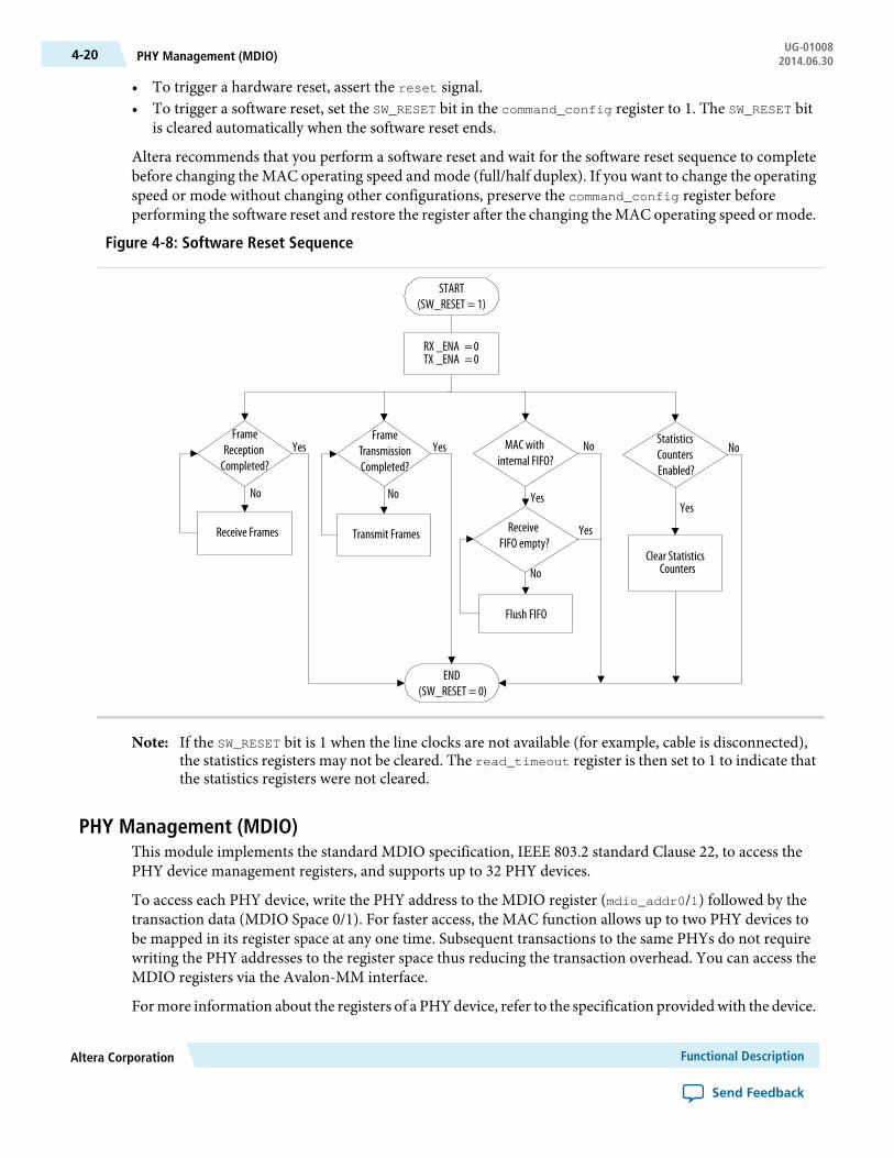
• To trigger a hardware reset, assert the reset signal.• To trigger a software reset, set the SW_RESET bit in the command_config register to 1. The SW_RESET bit
is cleared automatically when the software reset ends.
Altera recommends that you perform a software reset and wait for the software reset sequence to completebefore changing the MAC operating speed and mode (full/half duplex). If you want to change the operatingspeed or mode without changing other configurations, preserve the command_config register beforeperforming the software reset and restore the register after the changing the MAC operating speed or mode.
Figure 4-8: Software Reset Sequence
Receive Frames Transmit Frames
Flush FIFO
Clear StatisticsCounters
Yes Yes
Yes
No
No No Yes
No
Yes
No
RX _ENA =0TX _ENA =0
START(SW_RESET = 1)
END(SW_RESET = 0)
FrameReceptionCompleted?
FrameTransmissionCompleted?
MAC withinternal FIFO?
ReceiveFIFO empty?
StatisticsCountersEnabled?
If the SW_RESET bit is 1 when the line clocks are not available (for example, cable is disconnected),the statistics registers may not be cleared. The read_timeout register is then set to 1 to indicate thatthe statistics registers were not cleared.
Note:
PHY Management (MDIO)This module implements the standard MDIO specification, IEEE 803.2 standard Clause 22, to access thePHY device management registers, and supports up to 32 PHY devices.
To access each PHY device, write the PHY address to the MDIO register (mdio_addr0/1) followed by thetransaction data (MDIO Space 0/1). For faster access, the MAC function allows up to two PHY devices tobe mapped in its register space at any one time. Subsequent transactions to the same PHYs do not requirewriting the PHY addresses to the register space thus reducing the transaction overhead. You can access theMDIO registers via the Avalon-MM interface.
Formore information about the registers of a PHYdevice, refer to the specification providedwith the device.
Functional DescriptionAltera Corporation
Send Feedback
UG-01008PHY Management (MDIO)4-20 2014.06.30
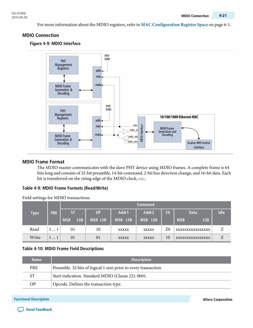
For more information about the MDIO registers, refer to MACConfiguration Register Space on page 6-1.
MDIO Connection
Figure 4-9: MDIO Interface
PHYAddr
MDIO FrameGeneration and
Decoding
MDIO
Inter
facemdc
mdio_in
mdio_out
mdio_oen
PHYAddrPHY
ManagementRegisters
MDIO FrameGeneration &
Decoding
mdio
mdc
addr
PHYManagementRegisters
MDIO FrameGeneration &
Decoding
mdio
mdc
addr
Avalon-MM ControlInterface
10/100/1000 Ethernet MAC
MDIO Frame FormatThe MDIO master communicates with the slave PHY device using MDIO frames. A complete frame is 64bits long and consists of 32-bit preamble, 14-bit command, 2-bit bus direction change, and 16-bit data. Eachbit is transferred on the rising edge of the MDIO clock, mdc.
Table 4-9: MDIO Frame Formats (Read/Write)
Field settings for MDIO transactions.Command
PREType IdleData
MSB LSB
TAAddr2
MSB LSB
Addr1
MSB LSB
OP
MSB LSB
ST
MSB LSB
ZxxxxxxxxxxxxxxxxZ0xxxxxxxxxx10011 ... 1Read
Zxxxxxxxxxxxxxxxx10xxxxxxxxxx01011 ... 1Write
Table 4-10: MDIO Frame Field Descriptions
DescriptionName
Preamble. 32 bits of logical 1 sent prior to every transaction.PRE
Start indication. Standard MDIO (Clause 22): 0b01.ST
Opcode. Defines the transaction type.OP
Altera CorporationFunctional Description
Send Feedback
4-21MDIO ConnectionUG-010082014.06.30
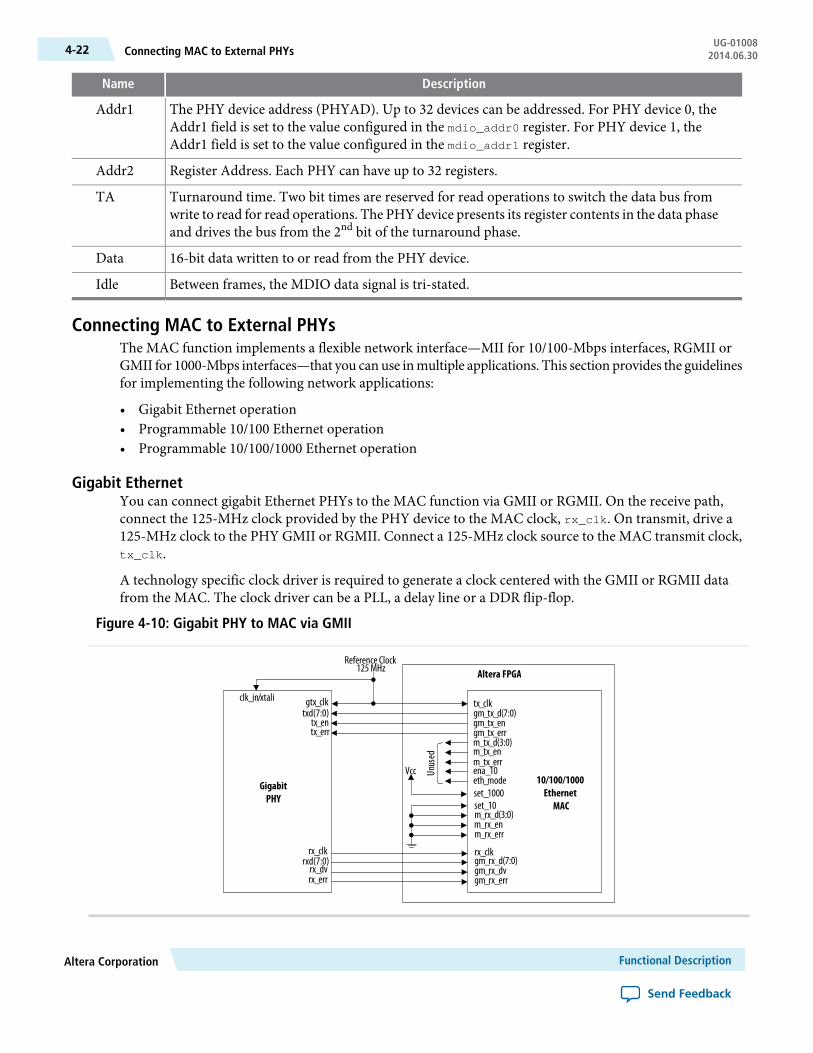
DescriptionName
The PHY device address (PHYAD). Up to 32 devices can be addressed. For PHY device 0, theAddr1 field is set to the value configured in the mdio_addr0 register. For PHY device 1, theAddr1 field is set to the value configured in the mdio_addr1 register.
Addr1
Register Address. Each PHY can have up to 32 registers.Addr2
Turnaround time. Two bit times are reserved for read operations to switch the data bus fromwrite to read for read operations. The PHY device presents its register contents in the data phaseand drives the bus from the 2nd bit of the turnaround phase.
TA
16-bit data written to or read from the PHY device.Data
Between frames, the MDIO data signal is tri-stated.Idle
Connecting MAC to External PHYsThe MAC function implements a flexible network interface—MII for 10/100-Mbps interfaces, RGMII orGMII for 1000-Mbps interfaces—that you can use inmultiple applications. This section provides the guidelinesfor implementing the following network applications:
• Gigabit Ethernet operation• Programmable 10/100 Ethernet operation• Programmable 10/100/1000 Ethernet operation
Gigabit EthernetYou can connect gigabit Ethernet PHYs to the MAC function via GMII or RGMII. On the receive path,connect the 125-MHz clock provided by the PHY device to the MAC clock, rx_clk. On transmit, drive a125-MHz clock to the PHY GMII or RGMII. Connect a 125-MHz clock source to the MAC transmit clock,tx_clk.
A technology specific clock driver is required to generate a clock centered with the GMII or RGMII datafrom the MAC. The clock driver can be a PLL, a delay line or a DDR flip-flop.
Figure 4-10: Gigabit PHY to MAC via GMII
Unus
ed
Altera FPGA
ena_10eth_mode
set_10set_1000
tx_clk
m_tx_d(3:0)m_tx_enm_tx_err
gm_tx_d(7:0)gm_tx_engm_tx_err
rx_clk
m_rx_d(3:0)m_rx_en
gm_rx_d(7:0)gm_rx_dvgm_rx_err
m_rx_err
Reference Clock125MHz
Vcc
clk_in/xtali gtx_clk
tx_entx_err
rx_clk
rx_dvrx_err
txd(7:0)
rxd(7:0)
10/100/1000Ethernet
MAC
GigabitPHY
Functional DescriptionAltera Corporation
Send Feedback
UG-01008Connecting MAC to External PHYs4-22 2014.06.30

Programmable 10/100 EthernetConnect 10/100 Ethernet PHYs to the MAC function via MII. On the receive path, connect the 25-MHz(100 Mbps) or 2.5-MHz (10 Mbps) clock provided by the PHY device to the MAC clock, rx_clk. On thetransmit path, connect the 25 MHz (100 Mbps) or a 2.5 MHz (10 Mbps) clock provided by the PHY to theMAC clock, tx_clk.
Figure 4-11: 10/100 PHY Interface
Unus
ed
Altera FPGA
Optional tie to 0if not used
Reference Clock25Mhz
ena_10eth_modeset_10set_1000
tx_clkm_tx_d(3:0)m_tx_enm_tx_errgm_tx_d(7:0)gm_tx_engm_tx_err
rx_clkm_rx_d(3:0)m_rx_en
gm_rx_d(7:0)gm_rx_dvgm_rx_err
m_rx_err
tx_clktxd(3:0)
tx_entx_err
clk_in/xtali
rx_clkrxd(3:0)
rx_dvrx_err
m_rx_colm_rx_crs
m_rx_colm_rx_crs
10/100/1000Ethernet
MAC10/100PHY
Programmable 10/100/1000 Ethernet OperationTypically, 10/100/1000 Ethernet PHYdevices implement a shared interface that you connect to a 10/100-MbpsMAC via MII/RGMII or to a gigabit MAC via GMII/RGMII.
On the receive path, connect the clock provided by the PHY device (2.5 MHz, 25 MHz or 125 MHz) to theMAC clock, rx_clk. The PHY interface is connected to both the MII (active PHY signals) and GMII of theMAC function.
On the transmit path, standard programmable PHY devices operating in 10/100 mode generate a 2.5 MHz(10 Mbps) or a 25 MHz (100 Mbps) clock. In gigabit mode, the PHY device expects a 125-MHz clock fromthe MAC function. Because the MAC function does not generate a clock output, an external clock moduleis introduced to drive the 125 MHz clock to the MAC function and PHY devices. In 10/100 mode, the clockgenerated by the MAC to the PHY can be tri-stated.
During transmission, the MAC control signal eth_mode selects either MII or GMII. The MAC functionasserts the eth_mode signal when the MAC function operates in gigabit mode, which subsequently drivesthe MAC GMII to the PHY interface. The eth_mode signal is deasserted when the MAC function operatesin 10/100 mode. In this mode, the MAC MII is driven to the PHY interface.
Altera CorporationFunctional Description
Send Feedback
4-23Programmable 10/100 EthernetUG-010082014.06.30

Figure 4-12: 10/100/1000 PHY Interface via MII/GMII
Altera FPGAx5
Unused
eth_modeset_1000set_10
tx_clk
m_tx_d(3:0)m_tx_enm_tx_errgm_tx_d(7:0)gm_tx_engm_tx_err
rx_clkm_rx_d(3:0)m_rx_en
gm_rx_d(7:0)gm_rx_dvgm_rx_err
m_rx_err
en_10
25MHzOsc
125 /25/2.5 MHz
25MHz
clk_in/xtali
25/2.5 MHz
gtx_clktxd(7:0)
tx_entx_err
tx_clk
rx_clk
rxd(7:0)rx_dvrx_err
ClockDriver
10/100/1000Ethernet
MAC
10/100/1000PHY
Optional tie to 0if not used
Figure 4-13: 10/100/1000 PHY Interface via RGMII
Altera FPGA
ena _10eth_mode
set _10set _1000
tx_clktx_controlrgmii _out [3:0]
rx_clkrx_controlrgmii _in[3:0]
Reference Clock125 MHz
gtx_clktx_en
txd [3:0]
rx_clkrx_dv
rxd [3:0]
clk _in/xtaliClockDivider
10/100/1000Ethernet
MAC10/100/1000
PHY
Optional tie to 0if not used
1000BASE-X/SGMII PCS With Optional Embedded PMAThe Altera 1000BASE-X/SGMII PCS function implements the functionality specified by IEEE 802.3 Clause36. The PCS function is accessible via MII (SGMII) or GMII (1000BASE-X/SGMII). The PCS functioninterfaces to an on- or off-chip SERDES component via the industry standard ten-bit interface (TBI).
Functional DescriptionAltera Corporation
Send Feedback
UG-010081000BASE-X/SGMII PCS With Optional Embedded PMA4-24 2014.06.30

You can configure the PCS function to include an embedded physical medium attachment (PMA) with a aserial transceiver or LVDS I/O and soft CDR. The PMA interoperates with an external physical mediumdependent (PMD) device, which drives the external copper or fiber network. The interconnect betweenAltera and PMD devices can be TBI or 1.25 Gbps serial.
The PCS function supports the following external PHYs:
• 1000 BASE-X PHYs as is.• 10BASE-T, 100BASE-T and 1000BASE-T PHYs if the PHYs support SGMII.
1000BASE-X/SGMII PCS ArchitectureFigure 4-14: 1000BASE-X/SGMII PCS
SGMIIReceiveConverter
SGMIITransmitConverter
Configuration
Encapsulation
De -encapsulation&
Synchronization
Auto-Negotiation
1000BASE -X/SGMII PCS
TBIReceive
TBITransmit
StatusLEDs
Avalon -MM Interface
MII/GMIIReceive
MII/GMIITransmit
Ethernet SideMAC Side
8b/10bDecoder
8b/10bEncoder
1000 Base-X PCS Receive Control
1000 Base-X PCS Transmit Control
Altera CorporationFunctional Description
Send Feedback
4-251000BASE-X/SGMII PCS ArchitectureUG-010082014.06.30

Figure 4-15: 1000BASE-X/SGMII PCS with Embedded PMA
SGMIIReceiveConverter
SGMIITransmitConverter
Configuration
Encapsulation
De -encapsulation&
Synchronization
Auto-Negotiation
StatusLEDs
Avalon -MM Interface
MII/GMIIReceive
MII/GMIITransmit
Serializer
PMA
PHYLoopback
Ethernet SideMAC Side
1000 Base-X PCS Receive Control
1000 Base-X PCS Transmit Control
8b/10bDecoder
8b/10bEncoder
1.25 GbpsSerial Receive
1.25 GbpsSerial Transmit
1000BASE-X/SGMII PCS with PMA
CDR &Deserializer
Transmit OperationThe transmit operation includes frame encapsulation and encoding.
Frame EncapsulationThe PCS function replaces the first preamble byte in the MAC frame with the start of frame /S/ symbol.Then, the PCS function encodes the rest of the bytes in the MAC frame with standard 8B/10B encodedcharacters. After the last FCS byte, the PCS function inserts the end of frame sequence, /T/ /R/ /R/ or /T//R/, depending on the number of character transmitted. Between frames, the PCS function transmits /I/symbols.
If the PCS function receives a frame from theMAC functionwith an error (gm_tx_err asserted during frametransmission), the PCS function encodes the error by inserting a /V/ character.
8b/10b EncodingThe 8B/10B encoder maps 8-bit words to 10-bit symbols to generate a DC balance and ensure disparity ofthe stream with a maximum run length of 5.
Functional DescriptionAltera Corporation
Send Feedback
UG-01008Transmit Operation4-26 2014.06.30
Receive OperationThe receive operation includes comma detection, decoding, de-encapsulation, synchronization, and carriersense.
Comma DetectionThe comma detection function searches for the 10-bit encoded comma character, K28.1/K28.5/K28.7, inconsecutive samples received from PMA devices. When the K28.1/K28.5/K28.7 comma code group isdetected, the PCS function realigns the data stream on a valid 10-bit character boundary. A standard 8b/10bdecoder can subsequently decodes the aligned stream.
The comma detection function restarts the search for a valid comma character if the receive synchronizationstate machine loses the link synchronization.
8b/10b DecodingThe 8b/10b decoder performs the disparity checking to ensure DC balancing and produces a decoded 8-bitstream of data for the frame de-encapsulation function.
Frame De-encapsulationThe frame de-encapsulation state machine detects the start of frame when the /I/ /S/ sequence is receivedand replaces the /S/ with a preamble byte (0x55). It continues decoding the frame bytes and transmits themto the MAC function. The /T/ /R/ /R/ or the /T/ /R/ sequence is decoded as an end of frame.
A /V/ character is decoded and sent to theMAC function as frame error. The statemachine decodes sequencesother than /I/ /I/ (Idle) or /I/ /S/ (Start of Frame) as wrong carrier.
During frame reception, the de-encapsulation state machine checks for invalid characters. When the statemachine detects invalid characters, it indicates an error to the MAC function.
SynchronizationThe link synchronization constantly monitors the decoded data stream and determines if the underlyingreceive channel is ready for operation. The link synchronization state machine acquires link synchronizationif the state machine receives three code groups with comma consecutively without error.
When link synchronization is acquired, the link synchronization statemachine counts the number of invalidcharacters received. The state machine increments an internal error counter for each invalid characterreceived and incorrectly positioned comma character. The internal error counter is decremented when fourconsecutive valid characters are received. When the counter reaches 4, the link synchronization is lost.
The PCS function drives the led_link signal to 1 when link synchronization is acquired. This signal can beused as a common visual activity check using a board LED.
Carrier SenseThe carrier sense state machine detects an activity when the link synchronization is acquired and when thetransmit and receive encapsulation or de-encapsulation state machines are not in the idle or error states.
The carrier sense state machine drives the mii_rx_crs and led_crs signals to 1 when it detects an activity.The led_crs signal can be used as a common visual activity check using a board LED.
Collision DetectionA collision happens when non-idle frames are received from the PHY and transmitted to the PHYsimultaneously. Collisions can be detected only in SGMII and half-duplex mode.
Altera CorporationFunctional Description
Send Feedback
4-27Receive OperationUG-010082014.06.30

When a collision happens, the collision detection state machine drives the mii_rx_col and led_col signalsto 1. You can use the led_col signal as a visual check using a board LED.
Transmit and Receive LatenciesAltera uses the following definitions for the transmit and receive latencies for the PCS function with anembedded PMA:
• Transmit latency is the time the PCS function takes to transmit the first bit on the PMA-PCS interfaceafter the bit was first available on the MAC side interface (MII/GMII).
• Receive latency is the time the PCS function takes to present the first bit on the MAC side interface(MII/GMII) after the bit was received on the PMA-PCS interface.
Table 4-11: PCS Transmit and Receive Latency
These latencies are derived from a simulation. For transceiver latency, refer to the transceiver handbook of therespective device family.
Latency (ns)PCS Configuration
ReceiveTransmit
PCS with GX transceivers
2489336810-Mbps SGMII
335488100-Mbps SGMII
1351841000-Mbps SGMII
40241000BASE-X
PCS with LVDS Soft-CDR I/O
2344360010-Mbps SGMII
344440100-Mbps SGMII
1841921000-Mbps SGMII
104401000BASE-X
SGMII ConverterYou can enable the SGMII converter by setting the SGMII_ENA bit in the if_mode register to 1.When enabledand the USE_SGMII_AN bit in the if_mode register is set to 1, the SGMII converter is automatically configuredwith the capabilities advertised by the PHY. Otherwise, Altera recommends that you configure the SGMIIconverter with the SGMII_SPEED bits in the if_mode register.
In 1000BASE-X mode, the PCS function always operates in gigabit mode and data duplication is disabled.
TransmitIn gigabitmode, the PCS andMAC functionsmust operate at the same rate. The transmit converter transmitseach byte from the MAC function once to the PCS function.
In 100-Mbps mode, the transmit converter replicates each byte received by the PCS function 10 times. In10Mbps, the transmit converter replicates each byte transmitted from theMAC function to the PCS function100 times.
Functional DescriptionAltera Corporation
Send Feedback
UG-01008Transmit and Receive Latencies4-28 2014.06.30

ReceiveIn gigabitmode, the PCS andMAC functionsmust operate at the same rate. The transmit converter transmitseach byte from the PCS function once to the MAC function.
In 100-Mbps mode, the receive converter transmits one byte out of 10 bytes received from the PCS functionto the MAC function. In 10-Mbps, the receive converter transmits one byte out of 100 bytes received fromthe PCS function to the MAC function.
Auto-NegotiationAuto-negotiation is an optional function that can be started when link synchronization is acquired duringsystem start up. To start auto-negotiation automatically, set the AUTO_NEGOTIATION_ENABLE bit in the PCScontrol register to 1. During auto-negotiation, the PCS function advertises its device features and exchangesthem with a link partner device.
If the SGMII_ENA bit in the if_mode register is set to 0, the PCS function operates in 1000BASE-X.Otherwise,the operatingmode is SGMII. The following sections describe the auto-negotiation process for each operatingmode.
When simulating your design, you can disable auto-negotiation to reduce the simulation time. If you enableauto-negotiation in your design, set the link_timer time to a smaller value to reduce the auto-negotiationlink timer in the simulation.
Related InformationPCS Configuration Register Space on page 6-18
1000BASE-X Auto-NegotiationWhen link synchronization is acquired, the PCS function starts sending a /C/ sequence (configurationsequence) to the link partner device with the advertised register set to 0x00. The sequence is sent for a timespecified in the PCS link_timer register mapped in the PCS register space.
When the link_timer time expires, the PCS dev_ability register is advertised, with the ACK bit set to 0for the link partner. The auto-negotiation state machine checks for three consecutive /C/ sequences receivedfrom the link partner.
The auto-negotiation state machine then sets the ACK bit to 1 in the advertised dev_ability register andchecks if three consecutive /C/ sequences are received from the link partner with the ACK bit set to 1.
Auto-negotiation waits for the value configured in the link_timer register to ensure no more consecutive/C/sequences are received from the link partner. The auto-negotiation is successfully completed when threeconsecutive idle sequences are received after the link timer expires.
After auto-negotiation completes successfully, the user software reads both the dev_ability andpartner_ability register and proceed to resolve priority for duplex mode and pause mode. If the designcontains a MAC and PCS, the user software configures the MAC with a proper resolved pause mode bysetting the PAUSE_IGNORE bit in command_config register. To disable pause frame generation based on thereceive FIFO buffer level, you should set the rx_section_empty register accordingly.
Altera CorporationFunctional Description
Send Feedback
4-29ReceiveUG-010082014.06.30

Figure 4-16: Auto-Negotiation Activity (Simplified)
Data
Link Partner PCS
LinkSynchronization
Acquired
Link Timer= 10 ms
/C/ with dev_ability register andACK bit set to 0
/C/ with dev_ability register andACK bit set to 1
Send /I/ (Idle) sequence
/C/ with 0x00 ability
3Consecutive/C/withAcknowledge
3Consecutive/C/LinkTim
erLinkTim
er
Once auto-negotiation completes successfully, the ability advertised by the link partner device is availablein the partner_ability register and the AUTO_NEGOTIATION_COMPLETE bit in the status register is set to 1.
The PCS function restarts auto-negotiation when link synchronization is lost and reacquired, or when youset the RESTART_AUTO_NEGOTIATION bit in the PCS control register to 1.
SGMII Auto-NegotiationIn SGMII mode, the capabilities of the PHY device are advertised and exchanged with a link partner PHYdevice.
Possible application of SGMII auto-negotiation in MAC mode and PHY mode.
Functional DescriptionAltera Corporation
Send Feedback
UG-01008SGMII Auto-Negotiation4-30 2014.06.30

Figure 4-17: SGMII Auto-Negotiation in MAC Mode and PHY Mode
SGMII PCS(MAC Mode)
SGMII Link
MediumTwistedCopperPair
Device Ability
Link Partner Ability
Altera Device
Triple Speed EthernetMegaCore Function
SGMII PCS with PMA(PHY Mode)
Device Ability
Link Partner Ability
Altera Device
Triple Speed EthernetMegaCore Function
Device Ability
10/100/1000BASE-T PHY 10/100/1000BASE-T PHYLink Partner
Link Partner Ability
Device Ability
Link Partner Ability
If the SGMII_ENA and USE_SGMII_AN bits in the if_mode register are 1, the PCS function is automaticallyconfigured with the capabilities advertised by the PHY device once the auto-negotiation completes.
If the SGMII_ENA bit is 1 and the USE_SGMII_AN bit is 0, the PCS function can be configured with theSGMII_SPEED and SGMII_DUPLEX bits in the if_mode register.
If the SGMII_ENA bit is 1 and the SGMII_AN_MODE bit is 1 (SGMII PHY Mode auto-negotiation is enabled)the speed and duplex mode resolution will be resolved based on the value that you set in the dev_abilityregister once auto negotiation is done. You should use set to the PHY mode if you want to advertise the linkspeed and duplex mode to the link partner.
Altera CorporationFunctional Description
Send Feedback
4-31SGMII Auto-NegotiationUG-010082014.06.30
Figure 4-18: SGMII Auto-Negotiation Activity
Link Timer= 1.6 ms
Data
PHY SGMII PCS
LinkSynchronization
Acquired
/C/ with 0x00 ability
/C/ with dev_ability/C/ with 0x0001
/C/ with dev_ability and ACK
Send /I/ (Idle) sequence
LinkTimer
LinkTimer
3Consecutive/C/3Consecutive/C/withAcknowledge
For more information, refer to CISCO Serial-GMII Specifications.
Ten-bit InterfaceIn PCS variations with embedded PMA, the PCS function implements a TBI to an external SERDES.
On transmit, the SERDES must serialize tbi_tx_d[0], the least significant bit of the TBI output bus firstand tbi_tx_d[9], the most significant bit of the TBI output bus last to ensure the remote node receives thedata correctly, as figure below illustrates.
Functional DescriptionAltera Corporation
Send Feedback
UG-01008Ten-bit Interface4-32 2014.06.30

Figure 4-19: SERDES Serialization Overview
serialization
tbi_tx_d(9:0)
1.25GbpsSerial Stream
9 0
On receive, the SERDES must serialize the TBI least significant bit first and the TBI most significant bit last,as figure below illustrates.
Figure 4-20: SERDES De-Serialization Overview
de-serialization
tbi_rx_d(9:0)
1.25GbpsSerial Stream
9 0
PHY LoopbackIn PCS variations with embedded PMA targeting devices with GX transceivers, you can enable loopback onthe serial interface to test the PCS and embedded PMA functions in isolation of the PMD. To enable loopback,set the sd_loopback bit in the PCS control register to 1.
The serial loopback option is not supported in Cyclone IV devices with GX transceiver.
Figure 4-21: Serial Loopback
SERDESTransmit
SERDESReceive
SERDES
Serial Receive
Serial TransmitPCS Transmit
PCS Receive
sd _ loopbackControl
MDIOSlave
1000BASE-X PCS
Ten-bitInterface
PHY Power-DownPower-down is controlled by the POWERDOWN bit in the PCS control register. When the system managementagent enables power-down, the PCS function drives the powerdown signal, which can be used to control atechnology specific circuit to switch off the PCS function clocks to reduce the application activity.
Altera CorporationFunctional Description
Send Feedback
4-33PHY LoopbackUG-010082014.06.30
When the PHY is in power-down state, the PCS function is in reset and any activities on the GMII transmitand the TBI receive interfaces are ignored. The management interface remains active and responds tomanagement transactions from the MAC layer device.
Figure 4-22: Power-Down
MDIOSlave
powerdownControl
Powerdown Control(Technology Specific)
1000BASE-X PCS
Power-Down in PCS Variations with Embedded PMAIn PCS variations with embedded PMA targeting devices with GX transceivers, the power-down signal isinternally connected to the power-down of theGX transceiver. In these devices, the power-down functionalityis shared across quad-port transceiver blocks. Ethernet designs must share a common gbx_pwrdn_in signalto use the same quad-port transceiver block.
For designs targeting devices other than Stratix V, you can export the power-down signals to implementyour own power-down logic to efficiently use the transceivers within a particular transceiver quad. Turn onthe Export transceiver powerdown signal parameter to export the signals.
Figure 4-23: Power-Down with Export Transceiver Power-Down Signal
PMA
POWERDOWNCONTROL
pcs_pwrdn_out
gxb_pwrdn_in
1000BASE-X PCS
1000BASE-X/SGMII PCS ResetA hardware reset resets all logic synchronized to the respective clock domains whereas a software reset onlyresets the PCS state machines, comma detection function, and 8B10B encoder and decoder. To trigger ahardware reset on the PCS, assert the respective reset signals: reset_reg_clk, reset_tx_clk, andreset_rx_clk. To trigger a software reset, set the RESET bit in the control register to 1.
In PCS variations with embedded PMA, assert the respective reset signals or the power-down signal to triggera hardware reset. Youmust assert the reset signal subsequent to asserting the reset_rx_clk, reset_tx_clk,or gbx_pwrdn_in signal. The reset sequence is also initiated when the active-low rx_freqlocked signal goeslow.
Functional DescriptionAltera Corporation
Send Feedback
UG-01008Power-Down in PCS Variations with Embedded PMA4-34 2014.06.30
Figure 4-24: Reset Distribution in PCS with Embedded PMA
PMA
ResetSequencer
ResetSynchronizer
ResetSynchronizer
PCS
reset
reset_tx_clkreset_rx_clk
gbx_pwrdn_in
rx_freqlocked
Formore information about the rx_freqlocked signal and transceiver reset, refer to the transceiver handbookof the respective device family.
Assert the reset or gxb_pwrdn_in signals to perform a hardware reset on MAC with PCS and embeddedPMA variation.
You must assert the reset signal for at least three clock cycles.Note:
Figure 4-25: Reset Distribution in MAC with PCS and Embedded PMA
PMA
ResetSequencer
ResetSynchronizer
ResetSynchronizer
MAC
reset gbx_pwrdwn
PCS
Altera IEEE 1588v2 FeatureThe Altera IEEE 1588v2 feature provides timestamp for receive and transmit frames in the Triple-SpeedEthernet MegaCore function designs. The feature consists of Precision Time Protocol (PTP). PTP is a layer-3protocol that accurately synchronizes all real time-of-day clocks in a network to a master clock.
This feature is supported in Arria V, Arria 10, Cyclone V, MAX10, and Stratix V device families.
IEEE 1588v2 Supported ConfigurationsThe Triple-Speed Ethernet MegaCore functions support the IEEE 1588v2 feature only in the followingconfigurations:
Altera CorporationFunctional Description
Send Feedback
4-35Altera IEEE 1588v2 FeatureUG-010082014.06.30

• 10/100/1000-MbpsMACwith 1000BASE-X/SGMII PCS and embedded serial PMAwithout FIFO bufferin full-duplex mode
• 10/100/1000-Mbps MAC with 1000BASE-X/SGMII PCS and embedded LVDS I/O without FIFO bufferin full-duplex mode
• 10/100/1000-Mbps MAC with 1000BASE-X/SGMII PCS• 10/100/1000-Mbps MAC without FIFO buffer in full-duplex mode
IEEE 1588v2 Features• Supports 4 types of PTP clock on the transmit datapath:
• Master and slave ordinary clock• Master and slave boundary clock• End-to-end (E2E) transparent clock• Peer-to-peer (P2P) transparent clock
• Supports PTP message types:
• PTP event messages—Sync, Delay_Req, Pdelay_Req, and Pdelay_Resp.• PTP generalmessages—Follow_Up,Delay_Resp, Pdelay_Resp_Follow_Up,Announce,Management,
and Signaling.
• Supports simultaneous 1-step and 2-step clock synchronizations on the transmit datapath.
• 1-step clock synchronization—The MAC function inserts accurate timestamp in Sync PTP messageor updates the correction field with residence time.
• 2-step clock synchronization—The MAC function provides accurate timestamp and the relatedfingerprint for all PTP message.
• Supports the following PHY operating speed accuracy:
• random error:
• 10Mbps—NA• 100Mbps—timestamp accuracy of ± 5 ns• 1000Mbps—timestamp accuracy of ± 2 ns
• static error—timestamp accuracy of ± 3 ns
• Supports IEEE 802.3, UDP/IPv4, and UDP/IPv6 transfer protocols for the PTP frames.• Supports untagged, VLAN tagged, Stacked VLAN Tagged PTP frames, and any number of MPLS labels.• Supports configurable register for timestamp correction on both transmit and receive datapaths.• Supports Time-of-Day (ToD) clock that provides a stream of 64-bit and 96-bit timestamps.
Functional DescriptionAltera Corporation
Send Feedback
UG-01008IEEE 1588v2 Features4-36 2014.06.30
IEEE 1588v2 ArchitectureFigure 4-26: Overview of the IEEE 1588v2 Feature
This figure shows only the datapaths related to the IEEE 1588v2 feature.
IEEE 1588v2Tx Logic
IEEE 1588v2Rx Logic
PTP SoftwareStack
Time-of-DayClock
PHYTx
PHYRx
MAC PHY
tx_path_delay
rx_path_delay
Timestamp &User Fingerprint
Correction
Time of Day
Timestamp Aligned toReceive Frame
tx_egress_timestamp_requesttx_ingress_timestamp
tx_time_of_dayrx_time_of_day
IEEE 1588v2 Transmit DatapathThe IEEE 1588v2 feature supports 1-step and 2-step clock synchronizations on the transmit datapath.
• For 1-step clock synchronization:
• Timestamp insertion depends on the PTP device and message type.• The MAC function inserts a timestamp in the Sync PTP message if the PTP clock operates as ordinary
or boundary clock.• Depending on the PTP device and message type, the MAC function updates the residence time in the
correction field of the PTP frame when the client assertstx_etstamp_ins_ctrl_residence_time_update. The residence time is the difference between theegress and ingress timestamps.
• For PTP frames encapsulated using the UDP/IPv6 protocol, the MAC function performs UDPchecksum correction using extended bytes in the PTP frame.
• The MAC function re-computes and re-inserts CRC-32 into the PTP frames after each timestamp orcorrection field insertion.
• For 2-step clock synchronization, theMAC function returns the timestamp and the associated fingerprintfor all transmit frames when the client asserts tx_egress_timestamp_request_valid.
Altera CorporationFunctional Description
Send Feedback
4-37IEEE 1588v2 ArchitectureUG-010082014.06.30
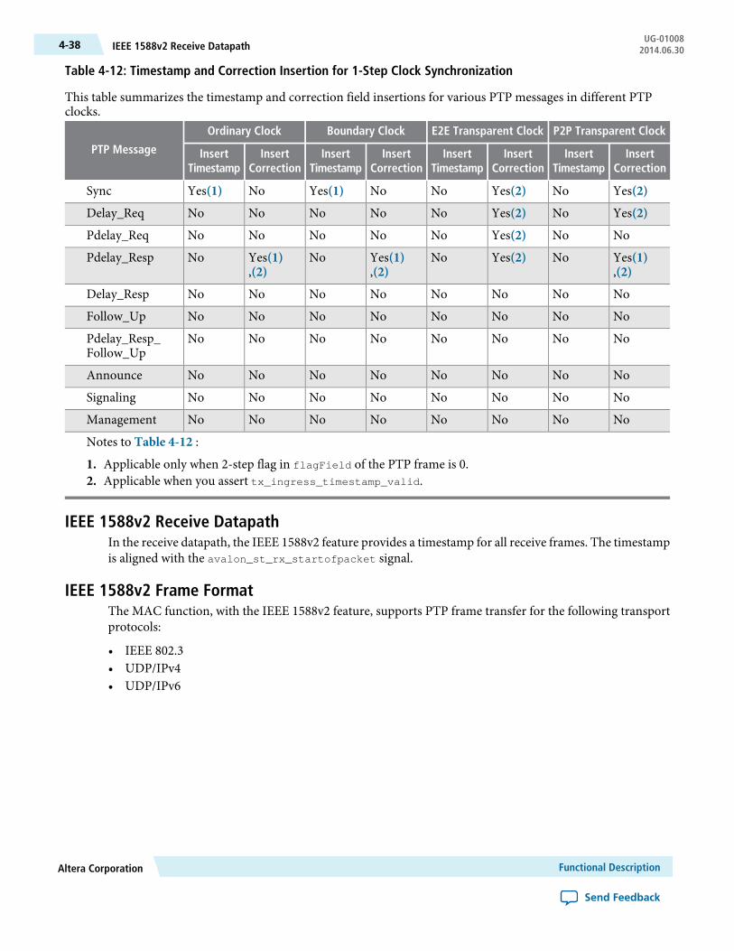
Table 4-12: Timestamp and Correction Insertion for 1-Step Clock Synchronization
This table summarizes the timestamp and correction field insertions for various PTP messages in different PTPclocks.
P2P Transparent ClockE2E Transparent ClockBoundary ClockOrdinary Clock
PTP Message InsertCorrection
InsertTimestamp
InsertCorrection
InsertTimestamp
InsertCorrection
InsertTimestamp
InsertCorrection
InsertTimestamp
Yes(2)NoYes(2)NoNoYes(1)NoYes(1)Sync
Yes(2)NoYes(2)NoNoNoNoNoDelay_Req
NoNoYes(2)NoNoNoNoNoPdelay_Req
Yes(1),(2)
NoYes(2)NoYes(1),(2)
NoYes(1),(2)
NoPdelay_Resp
NoNoNoNoNoNoNoNoDelay_Resp
NoNoNoNoNoNoNoNoFollow_Up
NoNoNoNoNoNoNoNoPdelay_Resp_Follow_Up
NoNoNoNoNoNoNoNoAnnounce
NoNoNoNoNoNoNoNoSignaling
NoNoNoNoNoNoNoNoManagement
Notes to Table 4-12 :
1. Applicable only when 2-step flag in flagField of the PTP frame is 0.2. Applicable when you assert tx_ingress_timestamp_valid.
IEEE 1588v2 Receive DatapathIn the receive datapath, the IEEE 1588v2 feature provides a timestamp for all receive frames. The timestampis aligned with the avalon_st_rx_startofpacket signal.
IEEE 1588v2 Frame FormatThe MAC function, with the IEEE 1588v2 feature, supports PTP frame transfer for the following transportprotocols:
• IEEE 802.3• UDP/IPv4• UDP/IPv6
Functional DescriptionAltera Corporation
Send Feedback
UG-01008IEEE 1588v2 Receive Datapath4-38 2014.06.30

PTP Frame in IEEE 802.3
Figure 4-27: PTP Frame in IEEE 8002.3
flagField
correctionField
transportSpecific | messageType
reserved | versionPTP
reserved
1 Octet
1 Octet
1 Octet
2 Octets
8 Octets
reserved4 Octets
SourcePortIdentify10 Octets
sequenceId2 Octets
controlField1 Octet
logMessageInterval1 Octet
TimeStamp10 Octets
domainNumber
messageLength2 Octets
1 Octet
Length/Type = 0x88F7
Source Address
Destination Address
2 Octets
6 Octets
6 Octets
MAC Header
PTP Header
0..1500/9600 Octets
CRC
Payload
4 Octets
(1)
Note to Figure 4–27 :
1. For frames with VLAN or Stacked VLAN tag, add 4 or 8 octets offsets before the length/type field.
PTP Frame over UDP/IPv4Checksum calculation is optional for the UDP/IPv4 protocol. The 1588v2 Tx logic should set the checksumto zero.
Altera CorporationFunctional Description
Send Feedback
4-39PTP Frame in IEEE 802.3UG-010082014.06.30

Figure 4-28: PTP Frame over UDP/IPv4
MAC Header
UDP Header
IP Header
PTP Header
Time To Live
Protocol = 0x11
Version | Internet Header Length
Differentiated Services
Flags | Fragment Offsets
1 Octet
1 Octet
2 Octets
1 Octet
1 Octet
Header Checksum2 Octets
Source IP Address4 Octets
Destination IP Address4 Octets
Options | Padding0 Octet
Source Port2 Octets
Destination Port = 319 / 3202 Octets
Identification
Total Length2 Octets
2 Octets
Length/Type = 0x0800
Source Address
Destination Address
2 Octets
6 Octets
6 Octets
Checksum
Length
2 Octets
2 Octets
flagField
correctionField
transportSpecific | messageType
reserved | versionPTP
reserved
1 Octet
1 Octet
1 Octet
2 Octets
8 Octets
reserved4 Octets
SourcePortIdentify10 Octets
sequenceId2 Octets
controlField1 Octet
logMessageInterval1 Octet
TimeStamp10 Octets
domainNumber
messageLength2 Octets
1 Octet
CRC4 Octets
(1)
0..1500/9600 Octets Payload
Note to Figure 4-28 :
1. For frames with VLAN or Stacked VLAN tag, add 4 or 8 octets offsets before the length/type field.
PTP Frame over UDP/IPv6Checksum calculation is mandatory for the UDP/IPv6 protocol. You must extend 2 bytes at the end of theUDP payload of the PTP frame. The MAC function modifies the extended bytes to ensure that the UDPchecksum remains uncompromised.
Functional DescriptionAltera Corporation
Send Feedback
UG-01008PTP Frame over UDP/IPv64-40 2014.06.30
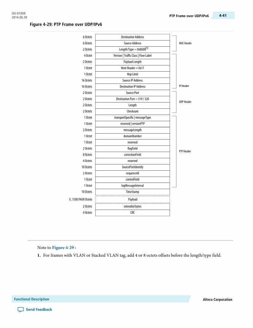
Figure 4-29: PTP Frame over UDP/IPv6
Version | Traffic Class | Flow Label
Payload Length
4 Octet
2 Octets
Source IP Address16 Octets
Destination IP Address16 Octets
Source Port2 Octets
Destination Port = 319 / 3202 Octets
Hop Limit
Next Header = 0x111 Octet
1 Octet
Length/Type = 0x86DD
Source Address
Destination Address
2 Octets
6 Octets
6 Octets
Checksum
Length
2 Octets
2 Octets
flagField
correctionField
transportSpecific | messageType
reserved | versionPTP
reserved
1 Octet
1 Octet
1 Octet
2 Octets
8 Octets
reserved4 Octets
SourcePortIdentify10 Octets
sequenceId2 Octets
controlField1 Octet
logMessageInterval1 Octet
TimeStamp10 Octets
extended bytes2 Octets
CRC4 Octets
domainNumber
messageLength2 Octets
1 Octet
MAC Header
UDP Header
IP Header
PTP Header
(1)
0..1500/9600 Octets Payload
Note to Figure 4-29 :
1. For frames with VLAN or Stacked VLAN tag, add 4 or 8 octets offsets before the length/type field.
Altera CorporationFunctional Description
Send Feedback
4-41PTP Frame over UDP/IPv6UG-010082014.06.30
5Triple-Speed Ethernet with IEEE 1588v2 DesignExample
2014.06.30
UG-01008 Subscribe Send Feedback
Software RequirementsAltera uses the following software to test the Triple-Speed Ethernet with IEEE 1588v2 design example andtestbench:
• Altera Complete Design Suite 14.0• ModelSim-SE 10.0b or higher
ISO9001:2008Registered
© 2014 Altera Corporation. All rights reserved. ALTERA, ARRIA, CYCLONE, ENPIRION, MAX, MEGACORE, NIOS, QUARTUS and STRATIX wordsand logos are trademarks of Altera Corporation and registered in the U.S. Patent and Trademark Office and in other countries. All otherwords and logos identified as trademarks or service marks are the property of their respective holders as described atwww.altera.com/common/legal.html. Altera warrants performance of its semiconductor products to current specifications in accordance withAltera's standard warranty, but reserves the right to make changes to any products and services at any time without notice. Altera assumesno responsibility or liability arising out of the application or use of any information, product, or service described herein except as expresslyagreed to in writing by Altera. Altera customers are advised to obtain the latest version of device specifications before relying on any publishedinformation and before placing orders for products or services.
www.altera.com
101 Innovation Drive, San Jose, CA 95134
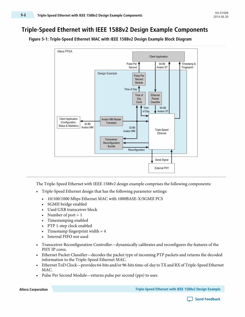
Triple-Speed Ethernet with IEEE 1588v2 Design Example ComponentsFigure 5-1: Triple-Speed Ethernet MAC with IEEE 1588v2 Design Example Block Diagram
EthernetPacketClassifier
Pulse PerSecondModule
Time ofDayClock
Time of Day
Triple-SpeedEthernet
Avalon MM MasterTranslator
Client Application(Configuration,
Status & Statistics)
TransceiverReconfiguration
Bundle
External PHY
Serial Signal
64-BitAvalon ST
Timeof Day
32-BitAvalon MM
Reconfiguration
32-BitAvalon MM
64-BitAvalon ST
Pulse PerSecond
Timestamp &Fingerprint
Client Application
Altera FPGA
Design Example
The Triple-Speed Ethernet with IEEE 1588v2 design example comprises the following components:
• Triple-Speed Ethernet design that has the following parameter settings:
• 10/100/1000 Mbps Ethernet MAC with 1000BASE-X/SGMII PCS• SGMII bridge enabled• Used GXB transceiver block• Number of port = 1• Timestamping enabled• PTP 1-step clock enabled• Timestamp fingerprint width = 4• Internal FIFO not used
• Transceiver Reconfiguration Controller—dynamically calibrates and reconfigures the features of thePHY IP cores.
• Ethernet Packet Classifier—decodes the packet type of incoming PTP packets and returns the decodedinformation to the Triple-Speed Ethernet MAC.
• Ethernet ToDClock—provides 64-bits and/or 96-bits time-of-day to TX andRXof Triple-Speed EthernetMAC.
• Pulse Per Second Module—returns pulse per second (pps) to user.
Triple-Speed Ethernet with IEEE 1588v2 Design ExampleAltera Corporation
Send Feedback
UG-01008Triple-Speed Ethernet with IEEE 1588v2 Design Example Components5-2 2014.06.30

• Avalon-MM Master Translator—provides access to the registers of the following components throughthe Avalon-MM interface:
• Triple-Speed Ethernet MAC• Transceiver Reconfiguration Controller• ToD Clock
Base AddressesTable below lists the design example components that you can reconfigure to suit your verification objectives.To reconfigure the components, write to their registers using the base addresses listed in the table and theregister offsets described in the components' user guides.
Table 5-1: Base Addresses of Triple-Speed Ethernet MAC with IEEE 1588v2 Design Example Components
Base AddressComponent
0x0000Triple-Speed Ethernet
0x1000Time of Day Clock
0x2000Transceiver Reconfiguration Controller
Triple-Speed Ethernet MAC with IEEE 1588v2 Design Example FilesFigure 5-2: Triple-Speed Ethernet MAC with IEEE 1588v2 Design Example Folders
<ip_library>/ethernet/altera_eth_tse_design_example
tse_ieee1588
testbench
Table 5-2: Triple-Speed Ethernet MAC with IEEE 1588v2 Design Example Files
These files are located in the ..\tse_ieee1588 directory.DescriptionFile Name
The top-level entity file of the design example for verification in hardware.tse_1588_top.v
The Quartus II SDC constraint file for use with the TimeQuest timinganalyzer.
tse_1588_top.sdc
A Qsys file for the Triple-Speed Ethernet design example with IEEE1588v2 option enabled.
tse_1588.qsys
Tcl script to run testbench simulation.tb_run_simulation.tcl
Altera CorporationTriple-Speed Ethernet with IEEE 1588v2 Design Example
Send Feedback
5-3Base AddressesUG-010082014.06.30

Creating a New Triple-Speed Ethernet MAC with IEEE 1588v2 DesignYou can use the Quartus II software to create a new Triple-Speed Ethernet MAC with IEEE 1588v2 design.Altera provides a Qsys design example file that you can customize to facilitate the development of yourTriple-Speed Ethernet MAC with IEEE 1588v2 design.
1. Launch the Quartus II software and open the tse_1588.top.v file from the project directory.2. LaunchQsys from theToolsmenu and open the tse_1588.qsys file. By default, the design example targets
the Stratix V device family. To change the target family, click on the Project Settings tab and select thedesired device from the Device family list.
3. Turn off the additional module under the Use column if your design does not require it. This actiondisconnects the module from the Triple-Speed Ethernet MAC with IEEE 1588v2 system.
4. Double-click on triple_speed_ethernet_0 to launch the parameter editor.5. Specify the required parameters in the parameter editor.6. Click Finish.7. On the Generation tab, select either a Verilog HDL or VHDL simulation model and make sure that the
Create HDL design files for synthesis option is turned on.8. Click Generate to generate the simulation and synthesis files.
Triple-Speed Ethernet with IEEE 1588v2 TestbenchAltera provides a testbench for you to verify the Triple-Speed Ethernet with IEEE 1588v2 design example.The following sections describe the testbench, its components, and use.
The testbench operates in loopback mode. Figure 5-3 shows the flow of the packets in the design example.
Figure 5-3: Testbench Block Diagram
Loopbackon serialinterface
Testbench
Avalon-MM
Avalon-MMControlRegister
Avalon-STTransmitFrame
Generator
Avalon-STReceiveFrameMonitor
EthernetPacketMonitor
EthernetPacketMonitor
DUT
avalon_bfm_wrapper.sv
Avalon Driver
Avalon-ST
Avalon-ST
Triple-Speed Ethernet with IEEE 1588v2 Design ExampleAltera Corporation
Send Feedback
UG-01008Creating a New Triple-Speed Ethernet MAC with IEEE 1588v2 Design5-4 2014.06.30
The testbenches comprise the following modules:
• Device under test (DUT)—the design example.• Avalon driver—uses Avalon-STmaster bus functionalmodels (BFMs) to exercise the transmit and receive
paths. The driver also uses themaster Avalon-MMBFM to access the Avalon-MM interfaces of the designexample components.
• Packet monitors—monitors the transmit and receive datapaths, and displays the frames in the simulatorconsole.
Triple-Speed Ethernet with IEEE 1588v2 Testbench FilesThe <ip library>/ethernet/altera_eth_tse_design_example/tse_ieee1588/ testbench directory contains thetestbench files.
Table 5-3: Triple-Speed Ethernet with IEEE 1588v2 Testbench Files
DescriptionFile Name
A wrapper for the Avalon BFMs that the avalon_driver.sv file uses.avalon_bfm_wrapper.sv
A SystemVerilog HDL driver that utilizes the BFMs to exercise thetransmit and receive path, and access the Avalon-MM interface.
avalon_driver.sv
A SystemVerilog HDL testbench that contains parameters to configurethe BFMs. Because the configuration is specific to the DUT, you mustnot change the contents of this file.
avalon_if_params_pkg.sv
A SystemVerilog HDL testbench that monitors the Avalon-ST transmitand receive interfaces.
avalon_st_eth_packet_monitor.sv
ASystemVerilogHDLpackage that contains the default parameter settingsof the testbench.
default_test_params_pkg.sv
ASystemVerilogHDL class that defines the Ethernet frames. The avalon_driver.sv file uses this class.
eth_mac_frame.sv
A SystemVerilog HDL package that maps addresses to the Avalon-MMcontrol registers.
eth_register_map_params_pkg.sv
A SystemVerilog HDL class that defines the timestamp in the testbench.ptp_timestamp.sv
A SystemVerilog HDL testbench file that controls the flow of thetestbench.
tb_testcase.sv
The top-level testbench file. This file includes the customized Triple-Speed Ethernet MAC, which is the device under test (DUT), a clientpacket generator, and a client packet monitor along with other logicblocks.
tb_top.sv
A signal tracing macro script for use with the ModelSim simulationsoftware to display testbench signals.
wave.do
Triple-Speed Ethernet with IEEE 1588v2 Testbench Simulation FlowUpon a simulated power-on reset, each testbench performs the following operations:
1. Initializes the DUT by configuring the following options through the Avalon-MM interface:
Altera CorporationTriple-Speed Ethernet with IEEE 1588v2 Design Example
Send Feedback
5-5Triple-Speed Ethernet with IEEE 1588v2 Testbench FilesUG-010082014.06.30
• Configures the MAC. In the MAC, sets the transmit primary MAC address to EE-CC-88-CC-AA-EE,sets the speed to 1000 Mbps, enables TX and RX MAC, enables pad removal at receive, sets IPG to12, and sets maximum packet size to 1518.
• Configures PCS and SGMII interface to 1000BASE-X.• Configures Timestamp Unit in the MAC, by setting periods and path delay adjustments of the clocks.• Configures ToD clock by loading a predefined time value.• Configures clock mode of Packet Classifier to Ordinary Clock mode.
2. Starts packet transmission with different clock mode. The testbench sends a total of three packets:
• 1-step PTP Sync message over Ethernet• 1-step PTP Sync message over UDP/IPv4 with VLAN tag• 2-step PTP Sync message over UDP/IPv6 with stacked VLAN tag
3. Configures clock mode of Packet Classifier to End-to-end Transparent Clock mode.4. Starts packet transmission. The testbench sends a total of three packets:
• 1-step PTP Sync message over Ethernet• 1-step PTP Sync message over UDP/IPv4 with VLAN tag• 2-step PTP Sync message over UDP/IPv6 with stacked VLAN tag
5. Ends transmission.
Simulating Triple-Speed Ethernet with IEEE 1588v2 Testbench with ModelSim SimulatorTo use the ModelSim simulator to simulate the testbench design:
1. Copy the respective design example directory to your preferred project directory: tse_ieee1588 from<ip library>/ethernet/altera_eth_tse_design_example.
2. Launch Qsys from the Tools menu and open the tse_1588.qsys file.3. On the Generation tab, select either a Verilog HDL or VHDL simulation model.4. Click Generate to generate the simulation and synthesis files.5. Run the following command to set up the required libraries, to compile the generated IP Functional
simulation model, and to exercise the simulation model with the provided testbench:do tb_run.tcl
Triple-Speed Ethernet with IEEE 1588v2 Design ExampleAltera Corporation
Send Feedback
UG-01008Simulating Triple-Speed Ethernet with IEEE 1588v2 Testbench with ModelSim Simulator5-6 2014.06.30
6Configuration Register Space
2014.06.30
UG-01008 Subscribe Send Feedback
MAC Configuration Register SpaceUse the registers to configure the different aspects of the MAC function and retrieve its status and statisticscounters.
In multiport MACs, a contiguous register space is allocated for all ports and accessed via the Avalon-MMcontrol interface. For example, if the register space base address for the first port is 0x00, the base addressfor the next port is 0x100 and so forth. The registers that are shared among the instances occupy the registerspace of the first port. Updating these registers in the register space of other ports has no effect on theconfiguration.
Table 6-1: Overview of MAC Register Space
DescriptionSectionDword Offset
Base registers to configure the MAC function. At the minimum,you must configure the following functions:
• Primary MAC address (mac_0/mac_1)• Enable transmit and receive paths (TX_ENA and RX_ENA bits
in the command_config register)
The following registers are shared among all instances of amultiport MAC:
• rev
• scratch
• frm_length
• pause_quant
• mdio_addr0 and mdio_addr1
• tx_ipg_length
For more information about the base configuration registers,refer to Base Configuration Registers (Dword Offset 0x00 –0x17) on page 6-3.
Base Configuration0x00 – 0x17
Counters collecting traffic statistics. Formore information aboutthe statistics counters, refer to StatisticsCounters (DwordOffset0x18 – 0x38) on page 6-11.
Statistics Counters0x18 – 0x38
ISO9001:2008Registered
© 2014 Altera Corporation. All rights reserved. ALTERA, ARRIA, CYCLONE, ENPIRION, MAX, MEGACORE, NIOS, QUARTUS and STRATIX wordsand logos are trademarks of Altera Corporation and registered in the U.S. Patent and Trademark Office and in other countries. All otherwords and logos identified as trademarks or service marks are the property of their respective holders as described atwww.altera.com/common/legal.html. Altera warrants performance of its semiconductor products to current specifications in accordance withAltera's standard warranty, but reserves the right to make changes to any products and services at any time without notice. Altera assumesno responsibility or liability arising out of the application or use of any information, product, or service described herein except as expresslyagreed to in writing by Altera. Altera customers are advised to obtain the latest version of device specifications before relying on any publishedinformation and before placing orders for products or services.
www.altera.com
101 Innovation Drive, San Jose, CA 95134
DescriptionSectionDword Offset
Transmit and receive datapaths control register. For moreinformation about these registers, see Transmit and ReceiveCommand Registers (Dword Offset 0x3A – 0x3B) on page6-13.
Transmit Command0x3A
Receive Command0x3B
Upper 32 bits of selected statistics counters. These registers areused if you turn on the option to use extended statistics counters.For more information about these counters, refer to StatisticsCounters (Dword Offset 0x18 – 0x38) on page 6-11 .
Extended StatisticsCounters0x3C – 0x3E
Unused.Reserved0x3F
64-entry write-only hash table to resolve multicast addresses.Only bit 0 in each entry is significant. When you write a 1 to adword offset in the hash table, the MAC accepts all multicastMAC addresses that hash to the value of the address (bits 5:0).Otherwise, the MAC rejects the multicast address. This table iscleared during reset.
Hashing is not supported in 10/100 and 1000 Mbps Small MACcore variations.
Multicast Hash Table0x40 – 0x7F
MDIO Space 0 and MDIO Space 1 map to registers 0 to 31 ofthe PHY devices whose addresses are configured in the mdio_addr0 and mdio_addr1 registers respectively. For example,register 0 of PHY device 0 maps to dword offset 0x80, register 1maps to dword offset 0x81 and so forth.
Reading or writing to MDIO Space 0 or MDIO Space 1immediately triggers a correspondingMDIO transaction to reador write the PHY register. Only bits [15:0] of each register aresignificant. Write 0 to bits [31:16] and ignore them on reads.
If your variation does not include the PCS function, you can useMDIO Space 0 and MDIO Space 1 to map to two PHY devices.
If your MAC variation includes the PCS function, the PCSfunction is always device 0 and its configuration registers (PCSConfiguration Register Space on page 6-18) occupy MDIOSpace 0. You can use MDIO Space 1 to map to a PHY device.
MDIO Space 0
or PCSFunctionConfigura-tion
0x80 – 0x9F
MDIO Space 10xA0 – 0xBF
Supplementary unicast addresses. For more information aboutthese addresses, refer to SupplementaryAddress (DwordOffset0xC0 – 0xC7) on page 6-15.
Supplementary Address0xC0 – 0xC7
Unused.Reserved(1)0xC8 – 0xCF
Registers to configure the IEEE 1588v2 feature. For moreinformation about these registers, refer to IEEE 1588v2 Feature(Dword Offset 0xD0 – 0xD6) on page 6-16.
IEEE 1588v2 Feature0xD0– 0xD6
Unused.Reserved(1)0xD7 – 0xFF
Note to Table 6-1 :
1. Altera recommends that you set all bits in the reserved registers to 0 and ignore them on reads.
Configuration Register SpaceAltera Corporation
Send Feedback
UG-01008MAC Configuration Register Space6-2 2014.06.30

Base Configuration Registers (Dword Offset 0x00 – 0x17)Table 6-2 lists the base registers you can use to configure the MAC function. A software reset does not resetthese registers except the first two bits (TX_ENA and RX_ENA = 0) in the command_config register.
Table 6-2: Base Configuration Register Map
HW ResetDescriptionR/WNameDword
Offset
<IPversionnumber>
• Bits[15:0]—Set to the current version of theMegaCorefunction.
• Bits[31:16]—Customer specific revision, specified bythe CUST_VERSION parameter defined in the top-levelfile generated for the instance of the MegaCorefunction. These bits are set to 0 during the configura-tion of the MegaCore function.
ROrev0x00
0Scratch register. Provides a memory location for you totest the device memory operation.
RWscratch(1)0x01
0MAC configuration register. Use this register to controland configure the MAC function. The MAC functionstarts operation as soon as the transmit and receive enablebits in this register are turned on. Altera, therefore,recommends that you configure this register last.
See Command_Config Register (Dword Offset 0x02)on page 6-7 for the bit description.
RWcommand_config0x02
06-byte MAC primary address. The first four mostsignificant bytes of the MAC address occupy mac_0 inreverse order. The last two bytes of the MAC addressoccupy the two least significant bytes of mac_1 in reverseorder.
For example, if theMACaddress is 00-1C-23-17-4A-CB,the following assignments are made:
mac_0 = 0x17231c00
mac_1 = 0x0000CB4a
Ensure that you configure these registers with a validMAC address if you disable the promiscuous mode(PROMIS_EN bit in command_config = 0).
RWmac_00x03
0RWmac_10x04
1518• Bits[15:0]—16-bit maximum frame length in bytes.The MegaCore function checks the length of receiveframes against this value. Typical value is 1518.
In 10/100 and 1000 Small MAC core variations, thisregister is RO and the maximum frame length is fixedto 1518.
• Bits[31:16]—unused.
RW/
RO
frm_length0x05
Altera CorporationConfiguration Register Space
Send Feedback
6-3Base Configuration Registers (Dword Offset 0x00 – 0x17)UG-010082014.06.30
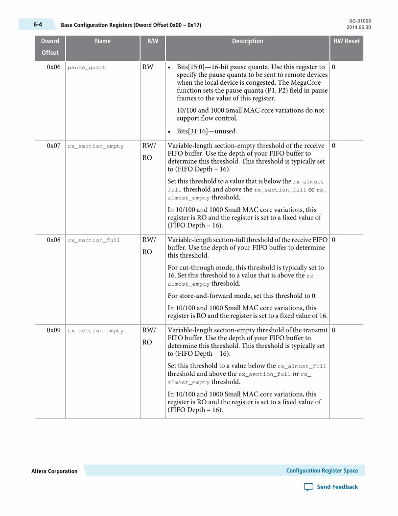
HW ResetDescriptionR/WNameDword
Offset
0• Bits[15:0]—16-bit pause quanta. Use this register tospecify the pause quanta to be sent to remote deviceswhen the local device is congested. The MegaCorefunction sets the pause quanta (P1, P2) field in pauseframes to the value of this register.
10/100 and 1000 Small MAC core variations do notsupport flow control.
• Bits[31:16]—unused.
RWpause_quant0x06
0Variable-length section-empty threshold of the receiveFIFO buffer. Use the depth of your FIFO buffer todetermine this threshold. This threshold is typically setto (FIFO Depth – 16).
Set this threshold to a value that is below the rx_almost_full threshold and above the rx_section_full or rx_almost_empty threshold.
In 10/100 and 1000 Small MAC core variations, thisregister is RO and the register is set to a fixed value of(FIFO Depth – 16).
RW/
RO
rx_section_empty0x07
0Variable-length section-full threshold of the receive FIFObuffer. Use the depth of your FIFO buffer to determinethis threshold.
For cut-through mode, this threshold is typically set to16. Set this threshold to a value that is above the rx_almost_empty threshold.
For store-and-forward mode, set this threshold to 0.
In 10/100 and 1000 Small MAC core variations, thisregister is RO and the register is set to a fixed value of 16.
RW/
RO
rx_section_full0x08
0Variable-length section-empty threshold of the transmitFIFO buffer. Use the depth of your FIFO buffer todetermine this threshold. This threshold is typically setto (FIFO Depth – 16).
Set this threshold to a value below the rx_almost_fullthreshold and above the rx_section_full or rx_almost_empty threshold.
In 10/100 and 1000 Small MAC core variations, thisregister is RO and the register is set to a fixed value of(FIFO Depth – 16).
RW/
RO
tx_section_empty0x09
Configuration Register SpaceAltera Corporation
Send Feedback
UG-01008Base Configuration Registers (Dword Offset 0x00 – 0x17)6-4 2014.06.30

HW ResetDescriptionR/WNameDword
Offset
0Variable-length section-full threshold of the transmitFIFO buffer. Use the depth of your FIFO buffer todetermine this threshold.
For cut-through mode, this threshold is typically set to16. Set this threshold to a value above the tx_almost_empty threshold.
For store-and-forward mode, set this threshold to 0.
In 10/100 and 1000 Small MAC core variations, thisregister is RO and the register is set to a fixed value of 16.
RW/
RO
tx_section_full0x0A
0Variable-length almost-empty threshold of the receiveFIFO buffer. Use the depth of your FIFO buffer todetermine this threshold.
Due to internal pipeline latency, you must set thisthreshold to a value greater than 3. This threshold istypically set to 8.
In 10/100 and 1000 Small MAC core variations, thisregister is RO and the register is set to a fixed value of 8.
RW/
RO
rx_almost_empty0x0B
0Variable-length almost-full threshold of the receive FIFObuffer. Use the depth of your FIFO buffer to determinethis threshold.
Due to internal pipeline latency, you must set thisthreshold to a value greater than 3. This threshold istypically set to 8.
In 10/100 and 1000 Small MAC core variations, thisregister is RO and the register is set to a fixed value of 8.
RW/
RO
rx_almost_full0x0C
0Variable-length almost-empty threshold of the transmitFIFO buffer. Use the depth of your FIFO buffer todetermine this threshold.
Due to internal pipeline latency, you must set thisthreshold to a value greater than 3. This threshold istypically set to 8.
In 10/100 and 1000 Small MAC core variations, thisregister is RO and the register is set to a fixed value of 8.
RW/
RO
tx_almost_empty0x0D
Altera CorporationConfiguration Register Space
Send Feedback
6-5Base Configuration Registers (Dword Offset 0x00 – 0x17)UG-010082014.06.30
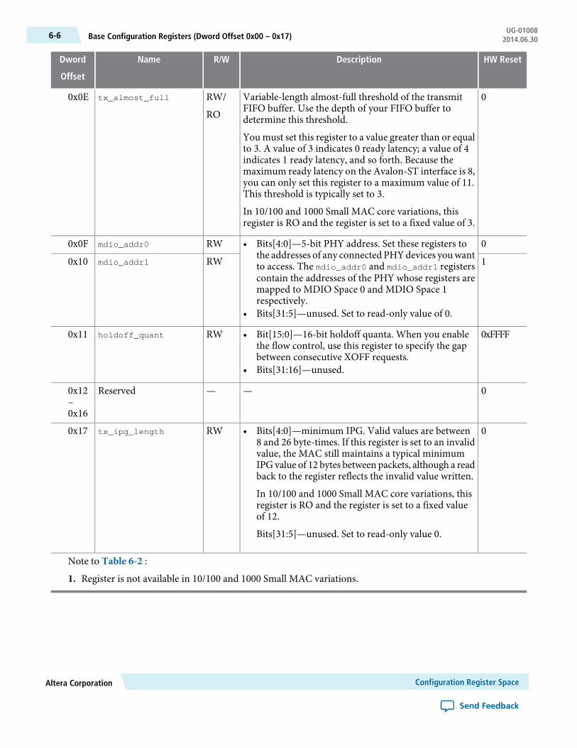
HW ResetDescriptionR/WNameDword
Offset
0Variable-length almost-full threshold of the transmitFIFO buffer. Use the depth of your FIFO buffer todetermine this threshold.
You must set this register to a value greater than or equalto 3. A value of 3 indicates 0 ready latency; a value of 4indicates 1 ready latency, and so forth. Because themaximum ready latency on the Avalon-ST interface is 8,you can only set this register to a maximum value of 11.This threshold is typically set to 3.
In 10/100 and 1000 Small MAC core variations, thisregister is RO and the register is set to a fixed value of 3.
RW/
RO
tx_almost_full0x0E
0• Bits[4:0]—5-bit PHY address. Set these registers tothe addresses of any connected PHYdevices youwantto access. The mdio_addr0 and mdio_addr1 registerscontain the addresses of the PHY whose registers aremapped to MDIO Space 0 and MDIO Space 1respectively.
• Bits[31:5]—unused. Set to read-only value of 0.
RWmdio_addr00x0F
1RWmdio_addr10x10
0xFFFF• Bit[15:0]—16-bit holdoff quanta. When you enablethe flow control, use this register to specify the gapbetween consecutive XOFF requests.
• Bits[31:16]—unused.
RWholdoff_quant0x11
0——Reserved0x12–0x16
0• Bits[4:0]—minimum IPG. Valid values are between8 and 26 byte-times. If this register is set to an invalidvalue, the MAC still maintains a typical minimumIPGvalue of 12 bytes between packets, although a readback to the register reflects the invalid value written.
In 10/100 and 1000 Small MAC core variations, thisregister is RO and the register is set to a fixed valueof 12.
Bits[31:5]—unused. Set to read-only value 0.
RWtx_ipg_length0x17
Note to Table 6-2 :
1. Register is not available in 10/100 and 1000 Small MAC variations.
Configuration Register SpaceAltera Corporation
Send Feedback
UG-01008Base Configuration Registers (Dword Offset 0x00 – 0x17)6-6 2014.06.30
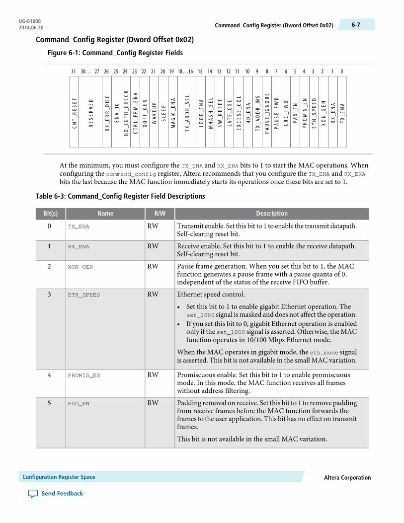
Command_Config Register (Dword Offset 0x02)
Figure 6-1: Command_Config Register Fields
TX_E
NA
RX_E
NA
XO
N_G
EN
ETH
_SPE
ED
PR
OM
IS_E
N
PAD
_EN
CR
C_F
WD
PAU
SE_F
WD
PAU
SE_I
GN
OR
E
TX_A
DD
R_I
NS
HD
_EN
A
EXC
ESS
_CO
L
LATE
_CO
L
SW
_RES
ET
MH
ASH
_SEL
LOO
P_EN
A
TX_A
DD
R_S
EL
MAG
IC_E
NA
SLE
EP
WAK
EUP
XOFF
_GEN
CTR
L_FR
M_E
NA
NO
_LG
TH_C
HEC
K
EN
A_10
RX_
ER
R_D
ISC
RESE
RV
ED
CN
T_R
ESET
31 30… 26 25 24 23 22 21 20 19 18…16 15 14 13 12 11 10 9 8 7 6 5 4 3 2 1 027
At the minimum, you must configure the TX_ENA and RX_ENA bits to 1 to start the MAC operations. Whenconfiguring the command_config register, Altera recommends that you configure the TX_ENA and RX_ENA
bits the last because the MAC function immediately starts its operations once these bits are set to 1.
Table 6-3: Command_Config Register Field Descriptions
DescriptionR/WNameBit(s)
Transmit enable. Set this bit to 1 to enable the transmit datapath.Self-clearing reset bit.
RWTX_ENA0
Receive enable. Set this bit to 1 to enable the receive datapath.Self-clearing reset bit.
RWRX_ENA1
Pause frame generation. When you set this bit to 1, the MACfunction generates a pause frame with a pause quanta of 0,independent of the status of the receive FIFO buffer.
RWXON_GEN2
Ethernet speed control.
• Set this bit to 1 to enable gigabit Ethernet operation. Theset_1000 signal ismasked and does not affect the operation.
• If you set this bit to 0, gigabit Ethernet operation is enabledonly if the set_1000 signal is asserted. Otherwise, the MACfunction operates in 10/100 Mbps Ethernet mode.
When the MAC operates in gigabit mode, the eth_mode signalis asserted. This bit is not available in the small MAC variation.
RWETH_SPEED3
Promiscuous enable. Set this bit to 1 to enable promiscuousmode. In this mode, the MAC function receives all frameswithout address filtering.
RWPROMIS_EN4
Padding removal on receive. Set this bit to 1 to remove paddingfrom receive frames before the MAC function forwards theframes to the user application. This bit has no effect on transmitframes.
This bit is not available in the small MAC variation.
RWPAD_EN5
Altera CorporationConfiguration Register Space
Send Feedback
6-7Command_Config Register (Dword Offset 0x02)UG-010082014.06.30

DescriptionR/WNameBit(s)
CRC forwarding on receive.
• Set this bit to 1 to forward the CRC field to the userapplication.
• Set this bit to 0 to remove the CRC field from receive framesbefore the MAC function forwards the frame to the userapplication.
• TheMAC function ignores this bit when it receives a paddedframe and the PAD_EN bit is 1. In this case, the MACfunction checks the CRC field and removes the checksumand padding from the frame before forwarding the frameto the user application.
RWCRC_FWD6
Pause frame forwarding on receive.
• Set this bit to 1 to forward receive pause frames to the userapplication.
• Set this bit to 0 to terminate and discard receive pauseframes.
RWPAUSE_FWD7
Pause frame processing on receive.
• Set this bit to 1 to ignore receive pause frames.• Set this bit to 0 to process receive pause frames. The MAC
function suspends transmission for an amount of timespecified by the pause quanta.
RWPAUSE_IGNORE8
MAC address on transmit.
• Set this bit to 1 to overwrite the source MAC address intransmit frames received from the user application with theMAC primary or supplementary address configured in theregisters. The TX_ADDR_SEL bit determines the addressselection.
• Set this bit to 0 to retain the sourceMAC address in transmitframes received from the user application.
RWTX_ADDR_INS9
Half-duplex enable.
• Set this bit to 1 to enable half-duplex.• Set this bit to 0 to enable full-duplex.• The MAC function ignores this bit if you set the ETH_SPEED
bit to 1.
RWHD_ENA10
Excessive collision condition.
• The MAC function sets this bit to 1 when it discards a frameafter detecting a collision on 16 consecutive frame retrans-missions.
• The MAC function clears this bit following a hardware orsoftware reset. See the SW_RESET bit description.
ROEXCESS_COL11
Configuration Register SpaceAltera Corporation
Send Feedback
UG-01008Command_Config Register (Dword Offset 0x02)6-8 2014.06.30
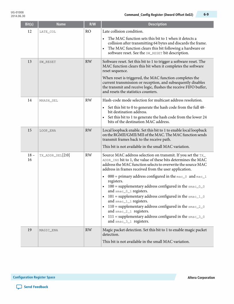
DescriptionR/WNameBit(s)
Late collision condition.
• The MAC function sets this bit to 1 when it detects acollision after transmitting 64 bytes and discards the frame.
• The MAC function clears this bit following a hardware orsoftware reset. See the SW_RESET bit description.
ROLATE_COL12
Software reset. Set this bit to 1 to trigger a software reset. TheMAC function clears this bit when it completes the softwarereset sequence.
When reset is triggered, the MAC function completes thecurrent transmission or reception, and subsequently disablesthe transmit and receive logic, flushes the receive FIFO buffer,and resets the statistics counters.
RWSW_RESET13
Hash-code mode selection for multicast address resolution.
• Set this bit to 0 to generate the hash code from the full 48-bit destination address.
• Set this bit to 1 to generate the hash code from the lower 24bits of the destination MAC address.
RWMHASH_SEL14
Local loopback enable. Set this bit to 1 to enable local loopbackon theRGMII/GMII/MII of theMAC.TheMAC function sendstransmit frames back to the receive path.
This bit is not available in the small MAC variation.
RWLOOP_ENA15
Source MAC address selection on transmit. If you set the TX_ADDR_INS bit to 1, the value of these bits determines the MACaddress theMAC function selects to overwrite the sourceMACaddress in frames received from the user application.
• 000 = primary address configured in the mac_0 and mac_1
registers.• 100 = supplementary address configured in the smac_0_0
and smac_0_1 registers.• 101 = supplementary address configured in the smac_1_0
and smac_1_1 registers.• 110 = supplementary address configured in the smac_2_0
and smac_2_1 registers.• 111 = supplementary address configured in the smac_3_0
and smac_3_1 registers.
RWTX_ADDR_SEL[2:0]18 –16
Magic packet detection. Set this bit to 1 to enable magic packetdetection.
This bit is not available in the small MAC variation.
RWMAGIC_ENA19
Altera CorporationConfiguration Register Space
Send Feedback
6-9Command_Config Register (Dword Offset 0x02)UG-010082014.06.30
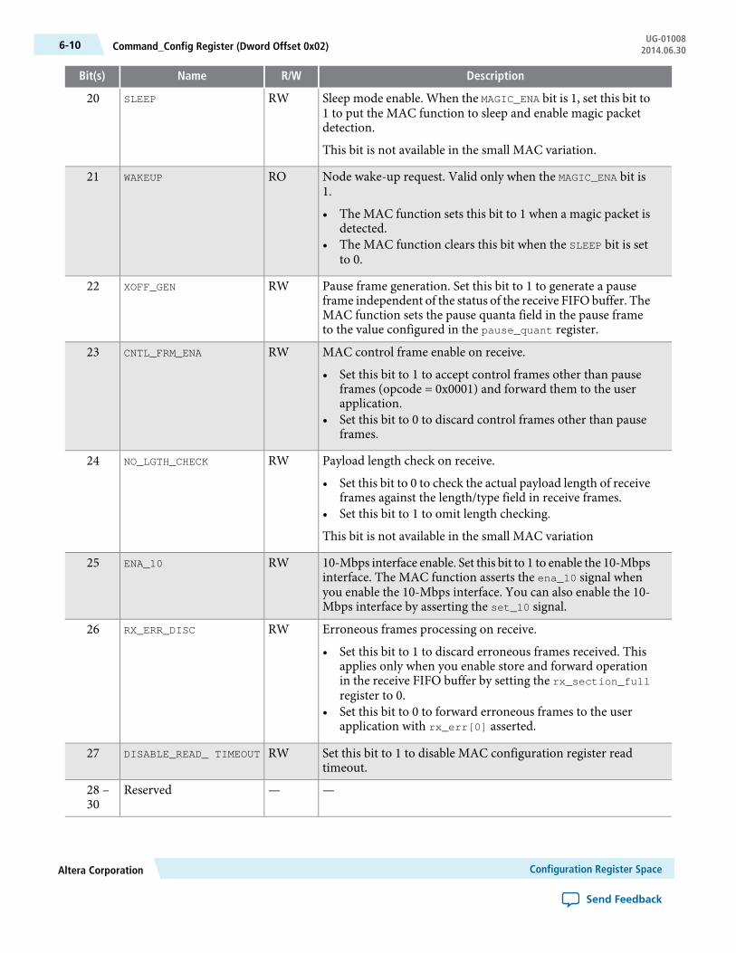
DescriptionR/WNameBit(s)
Sleep mode enable. When the MAGIC_ENA bit is 1, set this bit to1 to put the MAC function to sleep and enable magic packetdetection.
This bit is not available in the small MAC variation.
RWSLEEP20
Node wake-up request. Valid only when the MAGIC_ENA bit is1.
• The MAC function sets this bit to 1 when a magic packet isdetected.
• The MAC function clears this bit when the SLEEP bit is setto 0.
ROWAKEUP21
Pause frame generation. Set this bit to 1 to generate a pauseframe independent of the status of the receive FIFO buffer. TheMAC function sets the pause quanta field in the pause frameto the value configured in the pause_quant register.
RWXOFF_GEN22
MAC control frame enable on receive.
• Set this bit to 1 to accept control frames other than pauseframes (opcode = 0x0001) and forward them to the userapplication.
• Set this bit to 0 to discard control frames other than pauseframes.
RWCNTL_FRM_ENA23
Payload length check on receive.
• Set this bit to 0 to check the actual payload length of receiveframes against the length/type field in receive frames.
• Set this bit to 1 to omit length checking.
This bit is not available in the small MAC variation
RWNO_LGTH_CHECK24
10-Mbps interface enable. Set this bit to 1 to enable the 10-Mbpsinterface. The MAC function asserts the ena_10 signal whenyou enable the 10-Mbps interface. You can also enable the 10-Mbps interface by asserting the set_10 signal.
RWENA_1025
Erroneous frames processing on receive.
• Set this bit to 1 to discard erroneous frames received. Thisapplies only when you enable store and forward operationin the receive FIFO buffer by setting the rx_section_fullregister to 0.
• Set this bit to 0 to forward erroneous frames to the userapplication with rx_err[0] asserted.
RWRX_ERR_DISC26
Set this bit to 1 to disable MAC configuration register readtimeout.
RWDISABLE_READ_ TIMEOUT27
——Reserved28 –30
Configuration Register SpaceAltera Corporation
Send Feedback
UG-01008Command_Config Register (Dword Offset 0x02)6-10 2014.06.30

DescriptionR/WNameBit(s)
Statistics counters reset. Set this bit to 1 to clear the statisticscounters. The MAC function clears this bit when the resetsequence completes.
RWCNT_RESET31
Statistics Counters (Dword Offset 0x18 – 0x38)Table 6-4 describes the read-only registers that collect the statistics on the transmit and receive datapaths.A hardware reset clears these registers; a software reset also clears these registers except aMacID.
The register description uses the following definitions:
• Good frame—error-free frames with valid frame length.• Error frame—frames that contain errors or whose length is invalid.• Invalid frame—frames that are not addressed to the MAC function. The MAC function drops this frame.
Table 6-4: Statistics Counters
DescriptionR/WNameDword
Offset
The MAC address. This register is wired to the primary MACaddress in the mac_0 and mac_1 registers.
ROaMacID0x18–0x19
The number of frames that are successfully transmittedincluding the pause frames.
ROaFramesTransmittedOK0x1A
The number of frames that are successfully received includingthe pause frames.
ROaFramesReceivedOK0x1B
The number of receive frames with CRC error.ROaFrameCheck
SequenceErrors
0x1C
The number of receive frames with alignment error.ROaAlignmentErrors0x1D
The number of data and padding octets that are successfullytransmitted.
This register contains the lower 32 bits of the aOctetsTrans-mittedOK counter. The upper 32 bits of this statistics counterreside at the dword offset 0x0F.
ROaOctetsTransmittedOK0x1E
The number of data and padding octets that are successfullyreceived.
The lower 32 bits of the aOctetsReceivedOK counter. Theupper 32 bits of this statistics counter reside at the dword offset0x3D.
ROaOctetsReceivedOK0x1F
The number of pause frames transmitted.ROaTxPAUSEMACCtrlFrames0x20
The number received pause frames received.ROaRxPAUSEMACCtrlFrames0x21
The number of errored frames received.ROifInErrors0x22
Altera CorporationConfiguration Register Space
Send Feedback
6-11Statistics Counters (Dword Offset 0x18 – 0x38)UG-010082014.06.30

DescriptionR/WNameDword
Offset
The number of transmit frames with one the following errors:
• FIFO overflow error• FIFO underflow error• Errors defined by the user application
ROifOutErrors0x23
The number of valid unicast frames received.ROifInUcastPkts0x24
The number of valid multicast frames received. The countdoes not include pause frames.
ROifInMulticastPkts0x25
The number of valid broadcast frames received.ROifInBroadcastPkts0x26
This statistics counter is not in use.
The MAC function does not discard frames that are writtento the FIFO buffer by the user application.
—ifOutDiscards0x27
The number of valid unicast frames transmitted.ROifOutUcastPkts0x28
The number of valid multicast frames transmitted, excludingpause frames.
ROifOutMulticastPkts0x29
The number of valid broadcast frames transmitted.ROifOutBroadcastPkts0x2A
The number of frames that are dropped due to MAC internalerrors when FIFO buffer overflow persists.
ROetherStatsDropEvents0x2B
The total number of octets received. This count includes bothgood and errored frames.
This register is the lower 32 bits of etherStatsOctets. Theupper 32 bits of this statistics counter reside at the dword offset0x3E.
ROetherStatsOctets0x2C
The total number of good and errored frames received.ROetherStatsPkts0x2D
The number of frames received with length less than 64 bytes.This count does not include errored frames.
ROetherStatsUndersizePkts0x2E
The number of frames received that are longer than the valueconfigured in the frm_length register. This count does notinclude errored frames.
ROetherStatsOversizePkts0x2F
The number of 64-byte frames received. This count includesgood and errored frames.
ROetherStatsPkts64Octets0x30
The number of received good and errored frames between thelength of 65 and 127 bytes.
ROetherStatsPkts65to127Octets0x31
The number of received good and errored frames between thelength of 128 and 255 bytes.
ROetherStatsPkts128to255Octets0x32
The number of received good and errored frames between thelength of 256 and 511 bytes.
ROetherStatsPkts256to511Octets0x33
The number of received good and errored frames between thelength of 512 and 1023 bytes.
ROetherStatsPkts512to1023Octets0x34
Configuration Register SpaceAltera Corporation
Send Feedback
UG-01008Statistics Counters (Dword Offset 0x18 – 0x38)6-12 2014.06.30

DescriptionR/WNameDword
Offset
The number of received good and errored frames between thelength of 1024 and 1518 bytes.
ROetherStatsPkts1024to1518Octets0x35
The number of received good and errored frames between thelength of 1519 and the maximum frame length configured inthe frm_length register.
ROetherStatsPkts1519toXOctets0x36
Too long frames with CRC error.ROetherStatsJabbers0x37
Too short frames with CRC error.ROetherStatsFragments0x38
Unused—Reserved0x39
Extended Statistics Counters (0x3C – 0x3E)
Upper 32 bits of the respective statistics counters. By defaultall statistics counters are 32 bits wide. These statistics counterscan be extended to 64 bits by turning on the Enable 64-bitbyte counters parameter.
ROmsb_
aOctetsTransmittedOK
0x3C
ROmsb_aOctetsReceivedOK0x3D
ROmsb_etherStatsOctets0x3E
Transmit and Receive Command Registers (Dword Offset 0x3A – 0x3B)Table 6-5 describes the registers that determine how the MAC function processes transmit and receiveframes. A software reset does not change the values in these registers.
Altera CorporationConfiguration Register Space
Send Feedback
6-13Transmit and Receive Command Registers (Dword Offset 0x3A – 0x3B)UG-010082014.06.30
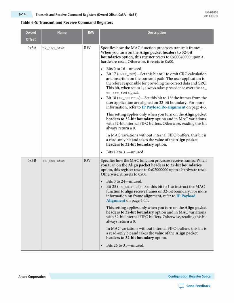
Table 6-5: Transmit and Receive Command Registers
DescriptionR/WNameDword
Offset
Specifies how the MAC function processes transmit frames.When you turn on the Align packet headers to 32-bitboundaries option, this register resets to 0x00040000 upon ahardware reset. Otherwise, it resets to 0x00.
• Bits 0 to 16—unused.• Bit 17 (OMIT_CRC)—Set this bit to 1 to omit CRC calculation
and insertion on the transmit path. The user application istherefore responsible for providing the correct data andCRC.This bit, when set to 1, always takes precedence over the ff_tx_crc_fwd signal.
• Bit 18 (TX_SHIFT16)—Set this bit to 1 if the frames from theuser application are aligned on 32-bit boundary. For moreinformation, refer to IP Payload Re-alignment on page 4-5.
This setting applies only when you turn on the Align packetheaders to 32-bit boundary option and in MAC variationswith 32-bit internal FIFO buffers. Otherwise, reading this bitalways return a 0.
In MAC variations without internal FIFO buffers, this bit isa read-only bit and takes the value of the Align packetheaders to 32-bit boundary option.
• Bits 19 to 31—unused.
RWtx_cmd_stat0x3A
Specifies how theMAC function processes receive frames.Whenyou turn on the Align packet headers to 32-bit boundariesoption, this register resets to 0x02000000 upon a hardware reset.Otherwise, it resets to 0x00.
• Bits 0 to 24—unused.• Bit 25 (RX_SHIFT16)—Set this bit to 1 to instruct the MAC
function to align receive frames on 32-bit boundary. Formoreinformation on frame alignment, refer to IP PayloadAlignment on page 4-11.
This setting applies only when you turn on the Align packetheaders to 32-bit boundary option and in MAC variationswith 32-bit internal FIFO buffers. Otherwise, reading this bitalways return a 0.
In MAC variations without internal FIFO buffers, this bit isa read-only bit and takes the value of the Align packetheaders to 32-bit boundary option.
• Bits 26 to 31—unused.
RWrx_cmd_stat0x3B
Configuration Register SpaceAltera Corporation
Send Feedback
UG-01008Transmit and Receive Command Registers (Dword Offset 0x3A – 0x3B)6-14 2014.06.30

Supplementary Address (Dword Offset 0xC0 – 0xC7)A software reset has no impact on these registers. MAC supplementary addresses are not available in 10/100and 1000 Small MAC variations.
Table 6-6: Supplementary Address Registers
HW ResetDescriptionR/WNameDword
Offset
0
You can specify up to four 6-byte supplementary addresses:
• smac_0_0/1• smac_1_0/1• smac_2_0/1• smac_3_0/1
Map the supplementary addresses to the respective registersin the same manner as the primary MAC address. Refer tothe description of mac_0 and mac_1.
The MAC function uses the supplementary addresses forthe following operations:
• to filter unicast frames when the promiscuous mode isdisabled (refer toCommand_ConfigRegister (DwordOffset 0x02) on page 6-7 for the description of thePROMIS_EN bit).
• to replace the source address in transmit frames receivedfrom the user application when address insertion isenabled (refer toCommand_Config Register (DwordOffset 0x02) on page 6-7 for the description of theTX_ADDR_INS and TX_ADDR_SEL bits).
If you do not require the use of supplementary addresses,configure them to the primary address.
RW
smac_0_00xC0
smac_0_10xC1
smac_1_00xC2
smac_1_10xC3
smac_2_00xC4
smac_2_10xC5
smac_3_00xC6
smac_3_10xC7
Altera CorporationConfiguration Register Space
Send Feedback
6-15Supplementary Address (Dword Offset 0xC0 – 0xC7)UG-010082014.06.30

IEEE 1588v2 Feature (Dword Offset 0xD0 – 0xD6)
Table 6-7: IEEE 1588v2 MAC Registers
HW ResetDescriptionR/WNameDwordOffset
0x0Clock period for timestamp adjustment on thetransmit datapath. The period register ismultiplied by the number of stages separatingactual timestamp and the GMII bus.
• Bits 0 to 15: Period in fractional nanoseconds(TX_PERIOD_FNS).
• Bits 16 to 24: Period in nanoseconds (TX_PERIOD_NS).
• Bits 25 to 31: Not used.
The default value for the period is 0. For 125-MHz clock, set this register to 8 ns.
RWtx_period0xD0
0x0Static timing adjustment in fractionalnanoseconds for outbound timestamps on thetransmit datapath.
• Bits 0 to 15: Timing adjustment in fractionalnanoseconds.
• Bits 16 to 31: Not used.
RWtx_adjust_fns0xD1
0x0Static timing adjustment in nanoseconds foroutbound timestamps on the transmit datapath.
• Bits 0 to 15: Timing adjustment in nanosec-onds.
• Bits 16 to 23: Not used.
RWtx_adjust_ns0xD2
0x0Clock period for timestamp adjustment on thereceive datapath. The period register ismultiplied by the number of stages separatingactual timestamp and the GMII bus.
• Bits 0 to 15: Period in fractional nanoseconds(RX_PERIOD_FNS).
• Bits 16 to 24: Period in nanoseconds (RX_PERIOD_NS).
• Bits 25 to 31: Not used.
The default value for the period is 0. For 125-MHz clock, set this register to 8 ns.
RWrx_period0xD3
Configuration Register SpaceAltera Corporation
Send Feedback
UG-01008IEEE 1588v2 Feature (Dword Offset 0xD0 – 0xD6)6-16 2014.06.30

HW ResetDescriptionR/WNameDwordOffset
0x0Static timing adjustment in fractionalnanoseconds for outbound timestamps on thereceive datapath.
• Bits 0 to 15: Timing adjustment in fractionalnanoseconds.
• Bits 16 to 31: Not used.
RWrx_adjust_fns0xD4
0x0Static timing adjustment in nanoseconds foroutbound timestamps on the receive datapath.
• Bits 0 to 15: Timing adjustment in nanosec-onds.
• Bits 16 to 23: Not used.
RWrx_adjust_ns0xD5
IEEE 1588v2 Feature PMA DelayPMA digital and analog delay of hardware for the IEEE 1588v2 feature and the register timing adjustment.1 UI is equivalent to 800 ps.
Table 6-8: IEEE 1588v2 Feature PMA Delay—Hardware
Timing AdjustmentDeviceDelay
RX registerTX register
26 UI53 UIStratix V or Arria V GZ
Digital 34 UI52 UIArria V GX, Arria V GT, or Arria V SoC
44 UI32 UICyclone V GX or Cyclone V SoC
1.75 ns-1.1 nsStratix V
Analog 1.75 ns-1.1 nsArria V
1.75 ns-1.1 nsCyclone V
Table 6-9: IEEE 1588v2 Feature LVDS I/O Delay—Hardware
Timing AdjustmentDeviceDelay
RX registerTX register
36 UI11 UIStratix V or Arria V GZDigital
36 UI11 UIArria V GX, Arria V GT, or Arria V SoC
PMA digital and analog delay of simulation model for the IEEE 1588v2 feature and the register timingadjustment.
Altera CorporationConfiguration Register Space
Send Feedback
6-17IEEE 1588v2 Feature PMA DelayUG-010082014.06.30

Table 6-10: IEEE 1588v2 Feature PMA Delay—Simulation Model
Timing AdjustmentDeviceDelay
RX registerTX register
33.5 UI11 UIStratix V or Arria V GZ
Digital23.5 UI10 UIArria V GX, Arria V GT, or Arria V SoC
23.5 UI32 UIArria 10
23.5 UI10 UICyclone V GX or Cyclone V SoC
Table 6-11: IEEE 1588v2 Feature LVDS I/O Delay—Simulation Model
Timing AdjustmentDeviceDelay
RX registerTX register
26 UI19.5 UIStratix V or Arria V GZ
Digital26 UI19.5 UIArria V GX, Arria V GT, or Arria V SoC
24.5 UI19.5 UIArria 10
26 UI19.5 UICyclone V GX or Cyclone V SoC
PCS Configuration Register SpaceThis section describes the PCS registers. Use the registers to configure the PCS function or retrieve its status.
In MAC and PCS variations, the PCS registers occupy the MAC register space and you access theseregisters via the MAC 32-bit Avalon-MM control interface. PCS registers are 16 bits wide, they
Note:
therefore occupy only the lower 16 bits and the upper 16 bits are set to 0. The offset of the first PCSregister in this variation is mapped to dword offset 0x80.
If you instantiate the IP core using the MegaWizard Plug-in Manager flow, use word addressing to accessthe register spaces. When you instantiate MAC and PCS variations, map the PCS registers to the respectivedword offsets in the MAC register space by adding the PCS word offset to the offset of the first PCS. Forexample,
• In PCS only variation, you can access the if_mode register at word offset 0x14.• In MAC and PCS variations, map the if_mode register to the MAC register space:
• Offset of the first PCS register = 0x80• if_mode word offset = 0x14• if_mode dword offset = 0x80 + 0x14 = 0x94
If you instantiate the MAC and PCS variation using the Qsys system, access the register spaces using byteaddressing. Convert the dword offsets to byte offsets by multiplying the dword offsets by 4. For example,
• For MAC registers:
• comand_config dword offset = 0x02• comand_config byte offset = 0x02 × 4 = 0x08
Configuration Register SpaceAltera Corporation
Send Feedback
UG-01008PCS Configuration Register Space6-18 2014.06.30

• For PCS registers, map the registers to the dword offsets in the MAC register space before you convertthe dword offsets to byte offsets:
• if_mode word offset = 0x14• if_mode dword offset = 0x80 + 0x14 = 0x94• if_mode byte offset = 0x94 × 4 = 0x250
Table 6-12: PCS Configuration Registers
DescriptionR/WRegister NameWord
Offset
PCS control register. Use this register to control andconfigure the PCS function. For the bit description, seeControl Register (Word Offset 0x00) on page 6-20.
RWcontrol0x00
Status register. Provides information on the operation ofthe PCS function.
ROstatus0x01
32-bit PHY identification register. This register is set to thevalue of the PHY ID parameter. Bits 31:16 are written toword offset 0x02. Bits 15:0 are written to word offset 0x03.
ROphy_identifier0x02
0x03
Use this register to advertise the device abilities to a linkpartner during auto-negotiation. In SGMIIMACmode, thePHYdoes not use this register during auto-negotiation. Forthe register bits description in 1000BASE-X and SGMIImode, see 1000BASE-X on page 6-23 and SGMII PHYMode Auto Negotiation on page 6-25.
RWdev_ability0x04
Contains the device abilities advertised by the link partnerduring auto-negotiation. For the register bits description in1000BASE-X and SGMII mode, refer to 1000BASE-X onpage 6-23 and SGMII PHY Mode Auto Negotiation onpage 6-25, respectively.
ROpartner_ability0x05
Auto-negotiation expansion register. Contains the PCSfunction capability and auto-negotiation status.
ROan_expansion0x06
The PCS function does not support these features. Theseregisters are always set to 0x0000 and any write access tothe registers is ignored.
RO
device_next_page0x07
partner_next_page0x08
master_slave_cntl0x09
master_slave_stat0x0A
——Reserved0x0B –0x0E
The PCS function does not implement extended statusregisters.
ROextended_status0x0F
Specific Extended Registers
Scratch register. Provides amemory location to test registerread and write operations.
RWscratch0x10
Altera CorporationConfiguration Register Space
Send Feedback
6-19PCS Configuration Register SpaceUG-010082014.06.30
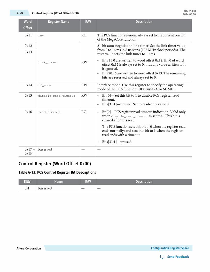
DescriptionR/WRegister NameWord
Offset
The PCS function revision. Always set to the current versionof the MegaCore function.
ROrev0x11
21-bit auto-negotiation link timer. Set the link timer valuefrom 0 to 16 ms in 8 ns steps (125 MHz clock periods). Thereset value sets the link timer to 10 ms.
• Bits 15:0 are written to word offset 0x12. Bit 0 of wordoffset 0x12 is always set to 0, thus any value written to itis ignored.
• Bits 20:16 are written toword offset 0x13. The remainingbits are reserved and always set to 0.
RWlink_timer
0x12
0x13
Interface mode. Use this register to specify the operatingmode of the PCS function; 1000BASE-X or SGMII.
RWif_mode0x14
• Bit[0]—Set this bit to 1 to disable PCS register readtimeout.
• Bits[31:1]—unused. Set to read-only value 0.
RWdisable_read_timeout0x15
• Bit[0]—PCS register read timeout indication. Valid onlywhen disable_read_timeout is set to 0. This bit iscleared after it is read.
The PCS function sets this bit to 0when the register readends normally; and sets this bit to 1 when the registerread ends with a timeout.
• Bits[31:1]—unused.
ROread_timeout0x16
——Reserved0x17 –0x1F
Control Register (Word Offset 0x00)
Table 6-13: PCS Control Register Bit Descriptions
DescriptionR/WNameBit(s)
——Reserved0:4
Configuration Register SpaceAltera Corporation
Send Feedback
UG-01008Control Register (Word Offset 0x00)6-20 2014.06.30
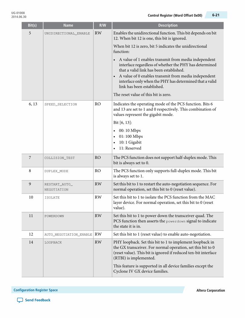
DescriptionR/WNameBit(s)
Enables the unidirectional function. This bit depends on bit12. When bit 12 is one, this bit is ignored.
When bit 12 is zero, bit 5 indicates the unidirectionalfunction:
• A value of 1 enables transmit from media independentinterface regardless of whether the PHY has determinedthat a valid link has been established.
• A value of 0 enables transmit from media independentinterface onlywhen the PHYhas determined that a validlink has been established.
The reset value of this bit is zero.
RWUNIDIRECTIONAL_ENABLE5
Indicates the operating mode of the PCS function. Bits 6and 13 are set to 1 and 0 respectively. This combination ofvalues represent the gigabit mode.
Bit [6, 13]:
• 00: 10 Mbps• 01: 100 Mbps• 10: 1 Gigabit• 11: Reserved
ROSPEED_SELECTION6, 13
The PCS function does not support half-duplex mode. Thisbit is always set to 0.
ROCOLLISION_TEST7
The PCS function only supports full-duplex mode. This bitis always set to 1.
RODUPLEX_MODE8
Set this bit to 1 to restart the auto-negotiation sequence. Fornormal operation, set this bit to 0 (reset value).
RWRESTART_AUTO_
NEGOTIATION
9
Set this bit to 1 to isolate the PCS function from the MAClayer device. For normal operation, set this bit to 0 (resetvalue).
RWISOLATE10
Set this bit to 1 to power down the transceiver quad. ThePCS function then asserts the powerdown signal to indicatethe state it is in.
RWPOWERDOWN11
Set this bit to 1 (reset value) to enable auto-negotiation.RWAUTO_NEGOTIATION_ENABLE12
PHY loopback. Set this bit to 1 to implement loopback inthe GX transceiver. For normal operation, set this bit to 0(reset value). This bit is ignored if reduced ten-bit interface(RTBI) is implemented.
This feature is supported in all device families except theCyclone IV GX device families.
RWLOOPBACK14
Altera CorporationConfiguration Register Space
Send Feedback
6-21Control Register (Word Offset 0x00)UG-010082014.06.30
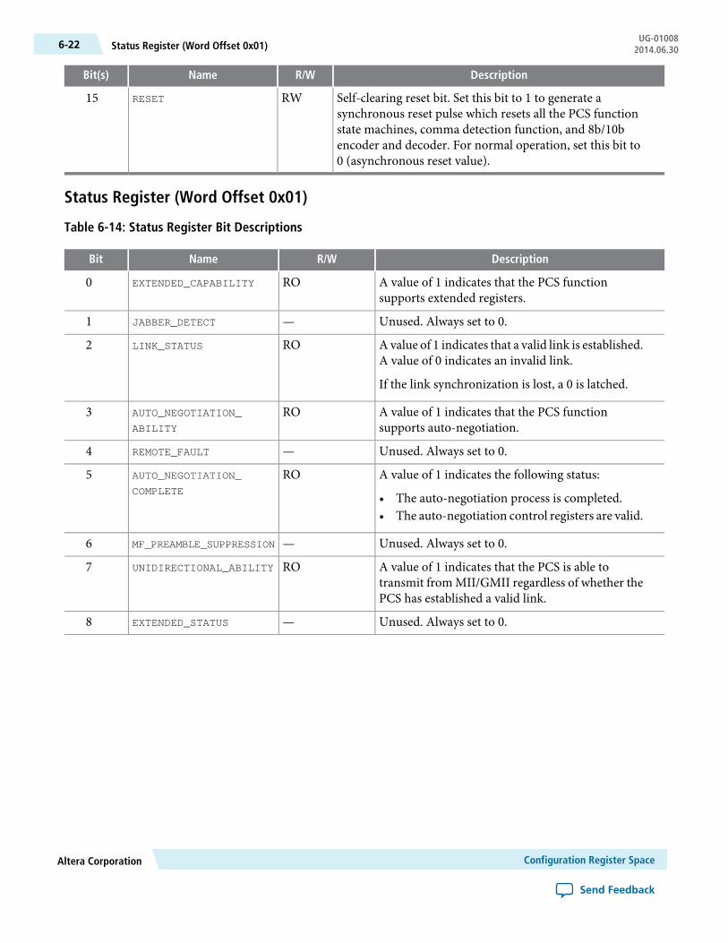
DescriptionR/WNameBit(s)
Self-clearing reset bit. Set this bit to 1 to generate asynchronous reset pulse which resets all the PCS functionstate machines, comma detection function, and 8b/10bencoder and decoder. For normal operation, set this bit to0 (asynchronous reset value).
RWRESET15
Status Register (Word Offset 0x01)
Table 6-14: Status Register Bit Descriptions
DescriptionR/WNameBit
A value of 1 indicates that the PCS functionsupports extended registers.
ROEXTENDED_CAPABILITY0
Unused. Always set to 0.—JABBER_DETECT1
A value of 1 indicates that a valid link is established.A value of 0 indicates an invalid link.
If the link synchronization is lost, a 0 is latched.
ROLINK_STATUS2
A value of 1 indicates that the PCS functionsupports auto-negotiation.
ROAUTO_NEGOTIATION_
ABILITY
3
Unused. Always set to 0.—REMOTE_FAULT4
A value of 1 indicates the following status:
• The auto-negotiation process is completed.• The auto-negotiation control registers are valid.
ROAUTO_NEGOTIATION_
COMPLETE
5
Unused. Always set to 0.—MF_PREAMBLE_SUPPRESSION6
A value of 1 indicates that the PCS is able totransmit from MII/GMII regardless of whether thePCS has established a valid link.
ROUNIDIRECTIONAL_ABILITY7
Unused. Always set to 0.—EXTENDED_STATUS8
Configuration Register SpaceAltera Corporation
Send Feedback
UG-01008Status Register (Word Offset 0x01)6-22 2014.06.30
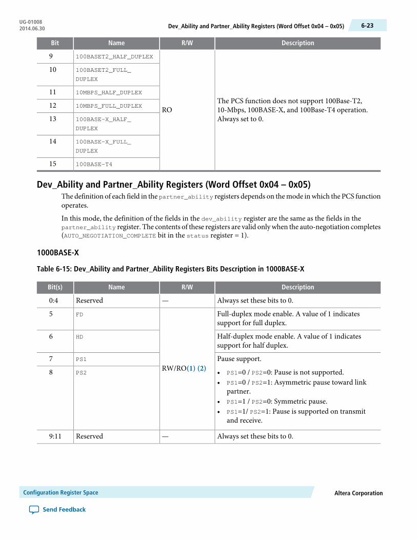
DescriptionR/WNameBit
The PCS function does not support 100Base-T2,10-Mbps, 100BASE-X, and 100Base-T4 operation.Always set to 0.
RO
100BASET2_HALF_DUPLEX9
100BASET2_FULL_
DUPLEX
10
10MBPS_HALF_DUPLEX11
10MBPS_FULL_DUPLEX12
100BASE-X_HALF_
DUPLEX
13
100BASE-X_FULL_
DUPLEX
14
100BASE-T415
Dev_Ability and Partner_Ability Registers (Word Offset 0x04 – 0x05)The definition of each field in the partner_ability registers depends on themode inwhich the PCS functionoperates.
In this mode, the definition of the fields in the dev_ability register are the same as the fields in thepartner_ability register. The contents of these registers are valid onlywhen the auto-negotiation completes(AUTO_NEGOTIATION_COMPLETE bit in the status register = 1).
1000BASE-X
Table 6-15: Dev_Ability and Partner_Ability Registers Bits Description in 1000BASE-X
DescriptionR/WNameBit(s)
Always set these bits to 0.—Reserved0:4
Full-duplex mode enable. A value of 1 indicatessupport for full duplex.
RW/RO(1) (2)
FD5
Half-duplex mode enable. A value of 1 indicatessupport for half duplex.
HD6
Pause support.
• PS1=0 / PS2=0: Pause is not supported.• PS1=0 / PS2=1: Asymmetric pause toward link
partner.• PS1=1 / PS2=0: Symmetric pause.• PS1=1/ PS2=1: Pause is supported on transmit
and receive.
PS17
PS28
Always set these bits to 0.—Reserved9:11
Altera CorporationConfiguration Register Space
Send Feedback
6-23Dev_Ability and Partner_Ability Registers (Word Offset 0x04 – 0x05)UG-010082014.06.30

DescriptionR/WNameBit(s)
Remote fault condition:
• RF1=0 / RF2=0: No error, link is valid (resetcondition).
• RF1=0 / RF2=1: Offline.• RF1=1 / RF2=0: Failure condition.• RF1=1 / RF2=1: Auto-negotiation error.
RW/RO(1) (2)
RF112
RF213
Acknowledge. A value of 1 indicates that the devicehas received three consecutive matching abilityvalues from its link partner.
ROACK14
Next page. In dev_ability register, this bit isalways set to 0.
RW/RO(1) (2)NP15
Notes to Table 6-15 :
1. All bits in the dev_ability register have RW access.2. All bits in the partner_ability register are read-only.
SGMII MAC Mode Auto NegotiationWhen the SGMII mode and the SGMII MAC mode auto-negotiation are enabled, the Triple-Speed EthernetIP core ignores the value in the dev_ability register and automatically sets the value to 16’h4001 as specifiedin the SGMII specification for SGMII auto-negotiation.
When the auto-negotiation is complete, the Triple-Speed Ethernet IP core speed and the duplex mode willbe resolved based on the value in the partner_ability register. The partner_ability register is receivedfrom the link partner during the auto-negotiation process.
Table 6-16: Partner_Ability Register Bits Description in SGMII MAC Mode
DescriptionR/WNameBit(s)
——Reserved9:0
Link partner interface speed:
• 00: copper interface speed is 10 Mbps• 01: copper interface speed is 100 Mbps• 10: copper interface speed is 1 gigabit• 11: reserved
ROCOPPER_SPEED[1:0]11:10
Link partner duplex capability:
• 1: copper interface is capable of operating in full-duplex mode
• 0: copper interface is capable of operating in half-duplex mode
ROCOPPER_DUPLEX_STATUS12
——Reserved13
Configuration Register SpaceAltera Corporation
Send Feedback
UG-01008SGMII MAC Mode Auto Negotiation6-24 2014.06.30
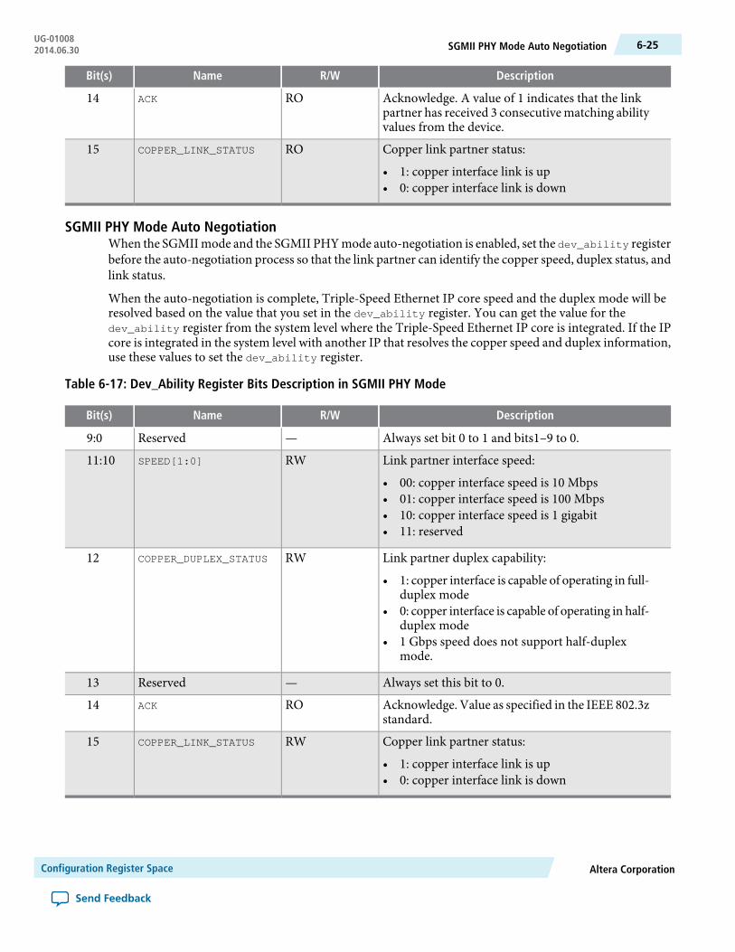
DescriptionR/WNameBit(s)
Acknowledge. A value of 1 indicates that the linkpartner has received 3 consecutive matching abilityvalues from the device.
ROACK14
Copper link partner status:
• 1: copper interface link is up• 0: copper interface link is down
ROCOPPER_LINK_STATUS15
SGMII PHY Mode Auto NegotiationWhen the SGMIImode and the SGMII PHYmode auto-negotiation is enabled, set the dev_ability registerbefore the auto-negotiation process so that the link partner can identify the copper speed, duplex status, andlink status.
When the auto-negotiation is complete, Triple-Speed Ethernet IP core speed and the duplex mode will beresolved based on the value that you set in the dev_ability register. You can get the value for thedev_ability register from the system level where the Triple-Speed Ethernet IP core is integrated. If the IPcore is integrated in the system level with another IP that resolves the copper speed and duplex information,use these values to set the dev_ability register.
Table 6-17: Dev_Ability Register Bits Description in SGMII PHY Mode
DescriptionR/WNameBit(s)
Always set bit 0 to 1 and bits1–9 to 0.—Reserved9:0
Link partner interface speed:
• 00: copper interface speed is 10 Mbps• 01: copper interface speed is 100 Mbps• 10: copper interface speed is 1 gigabit• 11: reserved
RWSPEED[1:0]11:10
Link partner duplex capability:
• 1: copper interface is capable of operating in full-duplex mode
• 0: copper interface is capable of operating in half-duplex mode
• 1 Gbps speed does not support half-duplexmode.
RWCOPPER_DUPLEX_STATUS12
Always set this bit to 0.—Reserved13
Acknowledge. Value as specified in the IEEE 802.3zstandard.
ROACK14
Copper link partner status:
• 1: copper interface link is up• 0: copper interface link is down
RWCOPPER_LINK_STATUS15
Altera CorporationConfiguration Register Space
Send Feedback
6-25SGMII PHY Mode Auto NegotiationUG-010082014.06.30
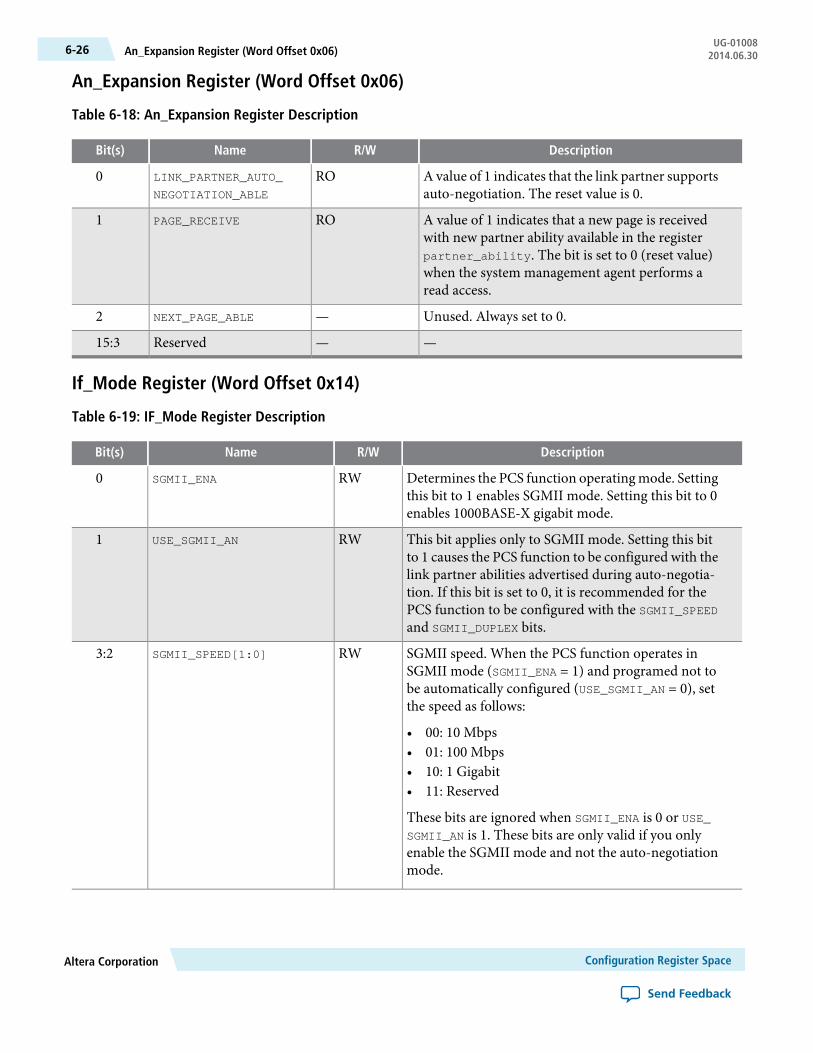
An_Expansion Register (Word Offset 0x06)
Table 6-18: An_Expansion Register Description
DescriptionR/WNameBit(s)
A value of 1 indicates that the link partner supportsauto-negotiation. The reset value is 0.
ROLINK_PARTNER_AUTO_
NEGOTIATION_ABLE
0
A value of 1 indicates that a new page is receivedwith new partner ability available in the registerpartner_ability. The bit is set to 0 (reset value)when the system management agent performs aread access.
ROPAGE_RECEIVE1
Unused. Always set to 0.—NEXT_PAGE_ABLE2
——Reserved15:3
If_Mode Register (Word Offset 0x14)
Table 6-19: IF_Mode Register Description
DescriptionR/WNameBit(s)
Determines the PCS function operating mode. Settingthis bit to 1 enables SGMII mode. Setting this bit to 0enables 1000BASE-X gigabit mode.
RWSGMII_ENA0
This bit applies only to SGMII mode. Setting this bitto 1 causes the PCS function to be configured with thelink partner abilities advertised during auto-negotia-tion. If this bit is set to 0, it is recommended for thePCS function to be configured with the SGMII_SPEEDand SGMII_DUPLEX bits.
RWUSE_SGMII_AN1
SGMII speed. When the PCS function operates inSGMII mode (SGMII_ENA = 1) and programed not tobe automatically configured (USE_SGMII_AN = 0), setthe speed as follows:
• 00: 10 Mbps• 01: 100 Mbps• 10: 1 Gigabit• 11: Reserved
These bits are ignored when SGMII_ENA is 0 or USE_SGMII_AN is 1. These bits are only valid if you onlyenable the SGMII mode and not the auto-negotiationmode.
RWSGMII_SPEED[1:0]3:2
Configuration Register SpaceAltera Corporation
Send Feedback
UG-01008An_Expansion Register (Word Offset 0x06)6-26 2014.06.30

DescriptionR/WNameBit(s)
SGMII half-duplex mode. Setting this bit to 1 enableshalf duplex for 10/100 Mbps speed. This bit is ignoredwhen SGMII_ENA is 0 or USE_SGMII_AN is 1. These bitsare only valid if you only enable the SGMII mode andnot the auto-negotiation mode.
RWSGMII_DUPLEX4
SGMII auto-negotiation mode:
• 1: enable SGMII PHY mode• 0: enable SGMII MAC mode
This bit resets to 0, which defaults to SGMII MACmode.
RWSGMII_AN_MODE5
——Reserved15:6
Register InitializationThe Triple-Speed Ethernet MegaCore function supports various types of interface commonly used by thefollowing Ethernet solutions:
• MII/GMII• RGMII• 10-bit Interface• SGMII• 1000BASE-X• Management Data Input/Output (MDIO) for external PHY register configuration
When using the Triple-Speed Ethernet MegaCore function with an external interface, you must understandthe requirements and initialize the registers.
Register initialization mainly performed in the following configurations:
• External PHY Initialization using MDIO (Optional)• PCS Configuration Register Initialization• MAC Configuration Register Initialization
This section discusses the register initialization for the following examples of the Ethernet system usingdifferent MAC interfaces with recommended initialization sequences:
• Triple-Speed Ethernet System with MII/GMII or RGMII on page 6-28• Triple-Speed Ethernet System with SGMII on page 6-30• Triple-Speed Ethernet System with 1000BASE-X Interface on page 6-31
Altera CorporationConfiguration Register Space
Send Feedback
6-27Register InitializationUG-010082014.06.30
Triple-Speed Ethernet System with MII/GMII or RGMIIFigure 6-2: Triple-Speed Ethernet System with MII/GMII or RGMII with Register Initialization Recommendation
10/100/1000 Mbps MAC External PHY
MACRegisterSpace
MDIO Space 0
MDIO Space 1 MDIOHost
PHYRegisterSpace
MDIOSlave
Avalon ST TX
Avalon ST RX
Avalon MM
Copper/FiberInterface
MII/GMII/RGMII Interface
MDIO
Use the following recommended initialization sequences for the example in Figure 6–2.
1. External PHY Initialization using MDIO
//Assume the External PHY Address is 0x0A
mdio_addr0 = 0x0A
//External PHY Register will Map to MDIO Space 0
Read/write to MDIO space 0 (dword offset 0x80 - 0x9F) = Read/write to PHY Register 0 to 31
2. MAC Configuration Register Initializationa. Disable MAC Transmit and Receive DatapathDisable the MAC transmit and receive datapath before
performing any changes to configuration.
//Set TX_ENA and RX_ENA bit to 0 in Command Config Register
Command_config Register = 0x00802220
//Read the TX_ENA and RX_ENA bit is set 0 to ensure TX and RX path is disable
Wait Command_config Register = 0x00802220
b. MAC FIFO Configuration
Tx_section_empty = Max FIFO size - 16
Tx_almost_full = 3
Tx_almost_empty = 8
Rx_section_empty = Max FIFO size - 16
Rx_almost_full = 8
Rx_almost_empty = 8
//Cut Throught Mode, Set this Threshold to 0 to enable Store and Forward Mode
Configuration Register SpaceAltera Corporation
Send Feedback
UG-01008Triple-Speed Ethernet System with MII/GMII or RGMII6-28 2014.06.30
Tx_section_full = 16
//Cut Throught Mode, Set this Threshold to 0 to enable Store and Forward Mode
Rx_section_full = 16
c. MAC Address Configuration
//MAC address is 00-1C-23-17-4A-CB
mac_0 = 0x17231C00
mac_1 = 0x0000CB4A
d. MAC Function Configuration
//Maximum Frame Length is 1518 bytes
Frm_length = 1518
//Minimum Inter Packet Gap is 12 bytes
Tx_ipg_length = 12
//Maximum Pause Quanta Value for Flow Control
Pause_quant = 0xFFFF
//Set the MAC with the following option:
// 100Mbps, User can get this information from the PHY status/PCS status
//Full Duplex, User can get this information from the PHY status/PCS status
//Padding Removal on Receive
//CRC Removal
//TX MAC Address Insertion on Transmit Packet
//Select mac_0 and mac_1 as the source MAC Address
Command_config Register = 0x00800220
e. Reset MACAltera recommends that you perform a software reset when there is a change in the MAC speed orduplex. The MAC software reset bit self-clears when the software reset is complete.
//Set SW_RESET bit to 1
Command_config Register = 0x00802220
Wait Command_config Register = 0x00800220
f. Enable MAC Transmit and Receive Datapath
//Set TX_ENA and RX_ENA to 1 in Command Config Register
Command_config Register = 0x00802223
//Read the TX_ENA and RX_ENA bit is set 1 to ensure TX and RX path is enable
Wait Command_config Register = 0x00802223
Altera CorporationConfiguration Register Space
Send Feedback
6-29Triple-Speed Ethernet System with MII/GMII or RGMIIUG-010082014.06.30

Triple-Speed Ethernet System with SGMIIFigure 6-3: Triple-Speed Ethernet System with SGMII with Register Initialization Recommendation
10/100/1000 Mbps MAC External PHY
MACRegisterSpace
MDIO Space 0
MDIO Space 1 MDIOHost
PHYRegisterSpace
MDIOSlave
Avalon ST TX
Avalon ST RX
Avalon MM
Copper/FiberInterface
SGMII Interface (1.25 Gbps)
MDIO
1000BASE-X/SGMII PCS
PCSRegisterSpace
Use the following recommended initialization sequences for the example in Figure 6–4.
1. External PHY Initialization using MDIO
Refer to step 1 in Triple-Speed Ethernet System with MII/GMII or RGMII on page 6-28.
2. PCS Configuration Register Initializationa. Set Auto Negotiation Link Timer
//Set Link timer to 1.6ms for SGMII
link_timer (address offset 0x12) = 0x0D40
Link_timer (address offset 0x13) = 0x03
b. Configure SGMII
//Enable SGMII Interface and Enable SGMII Auto Negotiation
//SGMII_ENA = 1, USE_SGMII_AN = 1
if_mode = 0x0003
c. Enable Auto Negotiation
//Enable Auto Negotiation
//AUTO_NEGOTIATION_ENA = 1, Bit 6,8,13 can be ignore
PCS Control Register = 0x1140
d. PCS Reset
//PCS Software reset is recommended where there any configuration changed
//RESET = 1
Configuration Register SpaceAltera Corporation
Send Feedback
UG-01008Triple-Speed Ethernet System with SGMII6-30 2014.06.30
PCS Control Register = 0x9140
Wait PCS Control Register RESET bit is clear
3. MAC Configuration Register Initialization
Refer to step 2 in Triple-Speed Ethernet System with MII/GMII or RGMII on page 6-28.
If 1000BASE-X/SGMII PCS is initialized, set the ETH_SPEED (bit 3) and ENA_10 (bit 25) incommand_config register to 0. If half duplex is reported in the PHY/PCS status register, set the HD_ENA(bit 10) to 1 in command_config register.
Note:
Triple-Speed Ethernet System with 1000BASE-X InterfaceFigure 6-4: Triple-Speed Ethernet System with 1000BASE-X Interface with Register InitializationRecommendation
10/100/1000 Mbps MAC 1000BASE-XOptical
Tranceiver (SFP)
MACRegisterSpace
MDIO Space 0
MDIO Space 1 MDIOHost
Avalon ST TX
Avalon ST RX
Avalon MM
FiberInterface
1000BASE-X Interface (1.25 Gbps)
1000BASE-X/SGMII PCS
PCSRegisterSpace
Use the following recommended initialization sequences for the example in Figure 6–5.
1. External PHY Initialization using MDIO
Refer to step 1 in Triple-Speed Ethernet System with MII/GMII or RGMII on page 6-28.
2. PCS Configuration Register Initializationa. Set Auto Negotiation Link Timer
//Set Link timer to 10ms for 1000BASE-X
link_timer (address offset 0x12) = 0x12D0
link_timer (address offset 0x13) = 0x13
b. Configure SGMII
//1000BASE-X/SGMII PCS is default in 1000BASE-X Mode
//SGMII_ENA = 0, USE_SGMII_AN = 0
if_mode = 0x0000
c. Enable Auto Negotiation
//Enable Auto Negotiation
Altera CorporationConfiguration Register Space
Send Feedback
6-31Triple-Speed Ethernet System with 1000BASE-X InterfaceUG-010082014.06.30
//AUTO_NEGOTIATION_ENA = 1, Bit 6,8,13 is Read Only
PCS Control Register = 0x1140
d. PCS Reset
//PCS Software reset is recommended where there any configuration changed
//RESET = 1
PCS Control Register = 0x9140
Wait PCS Control Register RESET bit is clear
3. MAC Configuration Register Initialization
Refer to step 2 in Triple-Speed Ethernet System with MII/GMII or RGMII on page 6-28.
If 1000BASE-X/SGMII PCS is initialized, set the ETH_SPEED (bit 3) and ENA_10 (bit 25) incommand_config register to 0. If half duplex is reported in the PHY/PCS status register, set the HD_ENA(bit 10) to 1 in command_config register.
Note:
Configuration Register SpaceAltera Corporation
Send Feedback
UG-01008Triple-Speed Ethernet System with 1000BASE-X Interface6-32 2014.06.30
7Interface Signals
2014.06.30
UG-01008 Subscribe Send Feedback
Interface SignalsThe following sections describe the Triple-Speed Ethernet MegaCore function interface signals:
• 10/100/1000 Ethernet MAC Signals on page 7-2• 10/100/1000 Multiport Ethernet MAC Signals on page 7-12• 10/100/1000 Ethernet MAC with 1000BASE-X/SGMII PCS Signals on page 7-16• 10/100/1000 Multiport Ethernet MAC with 1000BASE-X/SGMII PCS Signals on page 7-20• 10/100/1000EthernetMACwith 1000BASE-X/SGMIIPCS andEmbeddedPMASignals on page 7-22• 10/100/1000 Multiport Ethernet MAC with 1000BASE-X/SGMII PCS and Embedded PMA on page
7-25• 1000BASE-X/SGMII PCS Signals on page 7-34• 1000BASE-X/SGMII PCS and PMA Signals on page 7-38
To view all the interface signal names, turn on Show Signals in the BlockDiagram tab in the Triple-Speed Ethernet parameter editor interface. Otherwise, only the connection signal names are shown.
Note:
ISO9001:2008Registered
© 2014 Altera Corporation. All rights reserved. ALTERA, ARRIA, CYCLONE, ENPIRION, MAX, MEGACORE, NIOS, QUARTUS and STRATIX wordsand logos are trademarks of Altera Corporation and registered in the U.S. Patent and Trademark Office and in other countries. All otherwords and logos identified as trademarks or service marks are the property of their respective holders as described atwww.altera.com/common/legal.html. Altera warrants performance of its semiconductor products to current specifications in accordance withAltera's standard warranty, but reserves the right to make changes to any products and services at any time without notice. Altera assumesno responsibility or liability arising out of the application or use of any information, product, or service described herein except as expresslyagreed to in writing by Altera. Altera customers are advised to obtain the latest version of device specifications before relying on any publishedinformation and before placing orders for products or services.
www.altera.com
101 Innovation Drive, San Jose, CA 95134

10/100/1000 Ethernet MAC SignalsFigure 7-1: 10/100/1000 Ethernet MAC Function with Internal FIFO Buffers Signals
10/100/1000 Ethernet MAC
PHYManagementSignals
mdio_in
mdc
mdio_oen
mdio_out
Pause and MagicPacket Signals
xon_gen
xoff_gen
magic_wakeup
magic_sleep_n
ff_rx_clk
MACStatusSignals
ClockSignals
rx_clk
tx_clk
ResetSignal
reset
n
2
MAC TransmitInterface Signals
ff_tx_crc_fwd
ff_tx_data[DATAWIDTH-1:0]
ff_tx_eop
ff_tx_err
ff_tx_sop
ff_tx_wren
tx_ff_uflow
ff_tx_clk
ff_tx_rdy
ff_tx_septy
ff_tx_mod[1:0]
ff_tx_a_full
ff_tx_a_empty
2
n
6
18
4
MAC ReceiveInterface Signals
ff_rx_data[DATAWIDTH-1:0]
ff_rx_mod[1:0]
ff_rx_eop
ff_rx_sop
rx_err[5:0]
rx_err_stat[17:0]
rx_frm_type[3:0]
ff_rx_dsav
ff_rx_rdy
ff_rx_dval
ff_rx_a_full
ff_rx_a_empty
32
32
MAC ControlInterface
Signals
clk
reg_addr[7:0]
reg_rd
reg_wr
reg_data_out[31:0]
reg_data_in[31:0]
reg_busy
8
4
4
MIISignals
m_rx_d[3:0]m_rx_en
m_rx_err
m_rx_col
m_rx_crs
m_tx_d[3:0]
m_tx_en
m_tx_err
8
GMIISignals
gm_rx_d[7:0]
gm_rx_dv
gm_rx_err
gm_tx_d[7:0]
gm_tx_en
gm_tx_err
8
4
4
RGMIISignalsrgmii_out[3:0]
tx_control
rgmii_in[3:0]
rx_control
ECCStatusSignal
mac_eccstatus[1:0]
set_10_n
set_1000_n
ena_10_n
eth_mode_n
Clock and Reset SignalData transfers on the MAC Ethernet-side interface are synchronous to the receive and transmit clocks.
Table 7-1: GMII/RGMII/MII Clock Signal
DescriptionI/OName
GMII / RGMII/ MII transmit clock. Provides the timing reference forall GMII /MII transmit signals. The values of gm_tx_d[7:0], gm_tx_en, gm_tx_err, and of m_tx_d[3:0], m_tx_en, m_tx_err are validon the rising edge of tx_clk.
Itx_clk
Interface SignalsAltera Corporation
Send Feedback
UG-0100810/100/1000 Ethernet MAC Signals7-2 2014.06.30
DescriptionI/OName
GMII /RGMII/ MII receive clock. Provides the timing reference forall rx related signals. The values of gm_rx_d[7:0], gm_rx_dv, gm_rx_err, and of m_rx_d[3:0], m_rx_en, m_rx_err are valid on the risingedge of rx_clk.
Irx_clk
Table 7-2: Reset Signal
DescriptionI/OName
Assert this signal to reset all logic in the MAC and PCS controlinterface. The signal must be asserted for at least three clock cycles.
Ireset
MAC Control Interface SignalsThe MAC control interface is an Avalon-MM slave port that provides access to the register space.
Table 7-3: MAC Control Interface Signals
DescriptionI/OAvalon-MM SignalType
Name
Register access reference clock. Set the signal toa value less than or equal to 125 MHz.
Iclkclk
Register write enable.Iwritereg_wr
Register read enable.Ireadreg_rd
32-bit word-aligned register address.Iaddressreg_addr[7:0]
Register write data. Bit 0 is the least significantbit.
Iwritedatareg_data_in[31:0]
Register read data. Bit 0 is the least significant bit.Oreaddatareg_data_out[31:0]
Register interface busy. Asserted during registerread or register write access; deasserted when thecurrent register access completes.
Owaitrequestreg_busy
MAC Status SignalsThe MAC status signals which allow you to set the transfer mode of the Ethernet-side interface.
Table 7-4: MAC Status Signals
DescriptionI/OName
Ethernet mode. This signal is set to 1 when the MAC function isconfigured to operate at 1000 Mbps; set to 0 when it is configured tooperate at 10/100 Mbps.
Oeth_mode
10Mbps enable. This signal is set to 1 to indicate that the PHY interfaceshould operate at 10 Mbps. Valid only when the eth_mode signal is setto 0.
Oena_10
Altera CorporationInterface Signals
Send Feedback
7-3MAC Control Interface SignalsUG-010082014.06.30

DescriptionI/OName
Gigabit mode selection. Can be driven to 1 by an external device, forexample a PHY device, to set the MAC function to operate in gigabit.When set to 0, the MAC is set to operate in 10/100 Mbps. This signalis ignored when the ETH_SPEED bit in the command_config register isset to 1.
Iset_1000
10Mbps selection. Can be driven to 1 by an external device, for examplea PHY device, to indicate that the MAC function is connected to a 10-Mbps PHY device. When set to 0, the MAC function is set to operatein 100-Mbps or gigabit mode. This signal is ignored when the ETH_SPEED or ENA_10 bit in the command_config register is set to 1. TheENA_10 bit has a higher priority than this signal.
Iset_10
MAC Receive Interface Signals
Table 7-5: MAC Receive Interface Signals
DescriptionI/OAvalon-ST SignalType
Name
Avalon-ST Signals
Receive clock. All signals on theAvalon-ST receiveinterface are synchronized on the rising edge ofthis clock. Set this clock to the frequency requiredto get the desired bandwidth on this interface.This clock can be completely independent fromrx_clk.
Iclkff_rx_clk
Receive data valid. When asserted, this signalindicates that the data on the following signals arevalid: ff_rx_data[(DATAWIDTH -1):0], ff_rx_sop, ff_rx_eop, rx_err[5:0], rx_frm_type[3:0], and rx_err_stat[17:0].
Ovalidff_rx_dval
Receive data.When DATAWIDTH is 32, the first bytereceived is ff_rx_data[31:24] followed by ff_rx_data[23:16] and so forth.
Odataff_rx_data
[(DATAWIDTH-1):0]
Receive data modulo. Indicates invalid bytes inthe final frame word:
• 11: ff_rx_data[23:0] is not valid• 10: ff_rx_data[15:0] is not valid• 01: ff_rx_data[7:0] is not valid• 00: ff_rx_data[31:0] is valid
This signal applies only when DATAWIDTH is set to32.
Oemptyff_rx_mod[1:0]
Interface SignalsAltera Corporation
Send Feedback
UG-01008MAC Receive Interface Signals7-4 2014.06.30

DescriptionI/OAvalon-ST SignalType
Name
Receive start of packet. Asserted when the firstbyte or word of a frame is driven on ff_rx_
data[(DATAWIDTH-1):0].
Ostartofpacketff_rx_sop
Receive end of packet. Asserted when the last byteor word of frame data is driven on ff_rx_
data[(DATAWIDTH-1):0].
Oendofpacketff_rx_eop
Receive application ready. Assert this signal onthe rising edge of ff_rx_clk when the userapplication is ready to receive data from the MACfunction.
Ireadyff_rx_rdy
Receive error. Asserted with the final byte in theframe to indicate that an error was detected whenreceiving the frame. See Table 7-7 for the bitdescription.
Oerrorrx_err[5:0]
Component-Specific Signals
Receive frame available.When asserted, this signalindicates that the internal receive FIFO buffercontains some data to be read but not necessarilya complete frame. The user application may wantto start reading from the FIFO buffer.
This signal remains deasserted in the store andforward mode.
O—ff_rx_dsav
Frame type. See Table 7-6 for the bit description.O—rx_frm_type[3:0]
Assertedwhen the FIFObuffer reaches the almost-full threshold.
O—ff_rx_a_full
Asserted when the FIFO buffer goes below thealmost-empty threshold.
O—ff_rx_a_empty
rx_err_stat[17]: One indicates that the receiveframe is a stacked VLAN frame.
rx_err_stat[16]: One indicates that the receiveframe is either a VLAN or stacked VLAN frame.
rx_err_stat[15:0]: The value of the length/typefield of the receive frame.
O—rx_err_stat[17:0]
Table 7-6: rx_frm_type Bit Description
DescriptionBit
Indicates VLAN frames. Asserted with ff_rx_sop and remains asserted until the end of theframe.
3
Altera CorporationInterface Signals
Send Feedback
7-5MAC Receive Interface SignalsUG-010082014.06.30

DescriptionBit
Indicates broadcast frames. Asserted with ff_rx_sop and remains asserted until the end ofthe frame.
2
Indicates multicast frames. Asserted with ff_rx_sop and remains asserted until the end ofthe frame.
1
Indicates unicast frames. Asserted with ff_rx_sop and remains asserted until the end ofthe frame.
0
Table 7-7: rx_err Bit Description
DescriptionBit
Collision error. Asserted when the frame was received with a collision.5
Corrupted receive frame caused by PHY or PCS error. Asserted when the error is detectedon the MII/GMII/RGMII.
4
Truncated receive frame. Asserted when the receive frame is truncated due to an overflowin the receive FIFO buffer.
3
CRC error. Asserted when the frame is received with a CRC-32 error. This error bit appliesonly to frames with a valid length. Refer to Length Checking on page 4-10.
2 (1)
Invalid length error. Asserted when the receive frame has an invalid length as defined bythe IEEE Standard 802.3. For more information on the frame length, refer to LengthChecking on page 4-10 .
1 (1)
Receive frame error. Indicates that an error has occurred. It is the logical OR of rx_err[5:1].0
Note to Table 7-7 :
1. Bits 1 and 2 are not mutually exclusive. Ignore CRC error rx_err[2] signal if it is asserted at the sametime as the invalid length error rx_err[1] signal.
MAC Transmit Interface Signals
Table 7-8: MAC Transmit Interface Signals
DescriptionI/OAvalon-ST SignalType
Name
Avalon-ST Signals
Transmit clock. All transmit signals aresynchronized on the rising edge of this clock.
Set this clock to the required frequency to get thedesired bandwidth on the Avalon-ST transmitinterface. This clock can be completely indepen-dent from tx_clk.
Iclkff_tx_clk
Interface SignalsAltera Corporation
Send Feedback
UG-01008MAC Transmit Interface Signals7-6 2014.06.30
DescriptionI/OAvalon-ST SignalType
Name
Transmit data write enable. Assert this signal toindicate that the data on the following signals arevalid: ff_tx_data[(DATAWIDTH-1):0], ff_tx_sop, and ff_tx_eop.
In cut-through mode, keep this signal assertedthroughout the frame transmission. Otherwise,the frame is truncated and forwarded to theEthernet-side interface with an error.
Ivalidff_tx_wren
Transmit data. DATAWIDTH can be either 8 or 32depending on the FIFO data width configured.When DATAWIDTH is 32, the first byte transmittedis ff_tx_data[31:24] followed by ff_tx_data[23:16] and so forth.
Idataff_tx_data
[(DATAWIDTH-1):0]
Transmit datamodulo. Indicates invalid bytes inthe final frame word:
• 11: ff_tx_data[23:0] is not valid• 10: ff_tx_data[15:0] is not valid• 01: ff_tx_data[7:0] is not valid• 00: ff_tx_data[31:0] is valid
This signal applies only when DATAWIDTH is setto 32.
Iemptyff_tx_mod[1:0]
Transmit start of packet. Assert this signal whenthe first byte in the frame (the first byte of thedestination address) is driven on ff_tx_data.
Istartofpacketff_tx_sop
Transmit end of packet. Assert this signal whenthe last byte in the frame (the last byte of the FCSfield) is driven on ff_tx_data.
Iendofpacketff_tx_eop
Transmit frame error. Assert this signal with thefinal byte in the frame to indicate that thetransmit frame is invalid. The MAC functionforwards the invalid frame to the GMII with anerror.
Ierrorff_tx_err
MAC ready. When asserted, the MAC functionis ready to accept data from the user application.
Oreadyff_tx_rdy
Component-Specific Signals
Transmit CRC insertion. Set this signal to 0whenff_tx_eop is set to 1 to instruct the MACfunction to compute a CRC and insert it into theframe. If this signal is set to 1, the user applicationis expected to provide the CRC.
I—ff_tx_crc_fwd
Altera CorporationInterface Signals
Send Feedback
7-7MAC Transmit Interface SignalsUG-010082014.06.30
DescriptionI/OAvalon-ST SignalType
Name
Asserted when an underflow occurs on thetransmit FIFO buffer.
O—tx_ff_uflow
Deasserted when the FIFO buffer is filled to orabove the section-empty threshold defined in thetx_section_empty register. User applicationscan use this signal to indicate when to stopwriting to the FIFO buffer and initiate backpres-sure.
O—ff_tx_septy
Asserted when the transmit FIFO buffer reachesthe almost- full threshold.
O—ff_tx_a_full
Asserted when the transmit FIFO buffer goesbelow the almost-empty threshold.
O—ff_tx_a_empty
Pause and Magic Packet SignalsThe pause and magic packet signals are component-specific signals.
Table 7-9: Pause and Magic Packet Signals
DescriptionI/OName
Assert this signal for at least 1 tx_clk clock cycle to trigger thegeneration of a pause frame with a 0 pause quanta. The MAC functiongenerates the pause frame independent of the status of the receiveFIFO buffer.
This signal is not in use in the following conditions:
• Ignored when the xon_gen bit in the command_config register isset to 1.
• Absent when the Enable full duplex flow control option is turnedoff.
Ixon_gen
Assert this signal for at least one tx_clk clock cycle to trigger thegeneration of a pause frame with a pause quanta configured in thepause_quant register. The MAC function generates the pause frameindependent of the status of the receive FIFO buffer.
This signal is not in use in the following conditions:
• Ignored if the xoff_gen bit in the command_config register is setto 1.
• Absent when the Enable full duplex flow control option is turnedoff.
Ixoff_gen
Interface SignalsAltera Corporation
Send Feedback
UG-01008Pause and Magic Packet Signals7-8 2014.06.30

DescriptionI/OName
Assert this active-low signal to put the node into a power-down state.
If magic packets are supported (the MAGIC_ENA bit in the command_config register is set to 1), the receiver logic stops writing data to thereceive FIFO buffer and the magic packet detection logic is enabled.Setting this signal to 1 restores the normal frame reception mode.
This signal is present only if theEnablemagic packet detection optionis turned on.
Imagic_sleep_n
If the MAC function is in the power-down state, the MAC functionasserts this signal to indicate that a magic packet has been detectedand the node is requested to restore its normal frame reception mode.
This signal is present only if theEnablemagic packet detection optionis turned on.
0magic_wakeup
MII/GMII/RGMII Signals
Table 7-10: GMII/RGMII/MII Signals
DescriptionI/OName
GMII Transmit
GMII transmit data bus.Igm_tx_d[7:0]
Asserted to indicate that the data on the GMII transmit data bus isvalid.
Ogm_tx_en
Asserted to indicate to the PHY that the frame sent is invalid.Ogm_tx_err
GMII Receive
GMII receive data bus.Igm_rx_d[7:0]
Assert this signal to indicate that the data on the GMII receive data busis valid. Keep this signal asserted during frame reception, from the firstpreamble byte until the last byte of the CRC field is received.
Igm_rx_dv
The PHY asserts this signal to indicate that the receive frame containserrors.
Igm_rx_err
RGMII Transmit
RGMII transmit data bus. Drives gm_tx_d[3:0] on the positive edgeof tx_clk and gm_tx_d[7:4] on the negative edge of tx_clk.
Orgmii_out[3:0]
Control output signal. Drives gm_tx_en on the positive edge of tx_clkand a logical derivative of (gm_tx_en XOR gm_tx_err) on the negativeedge of tx_clk.
Otx_control
RGMII Receive
RGMII receive data bus. Expects gm_rx_d[3:0] on the positive edgeof rx_clk and gm_rx_d[7:4] on the negative edge of rx_clk.
Irgmii_in[3:0]
Altera CorporationInterface Signals
Send Feedback
7-9MII/GMII/RGMII SignalsUG-010082014.06.30
DescriptionI/OName
RGMII control input signal. Expects gm_rx_dv on the positive edge ofrx_clk and a logical derivative of (gm_rx_dv XOR gm_rx_err) on thenegative edge of rx_clk.
Irx_control
MII Transmit
MII transmit data bus.Om_tx_d[3:0]
Asserted to indicate that the data on the MII transmit data bus is valid.Om_tx_en
Asserted to indicate to the PHY device that the frame sent is invalid.Om_tx_err
MII Receive
MII receive data bus.Im_rx_d[3:0]
Assert this signal to indicate that the data on the MII receive data busis valid. Keep this signal asserted during frame reception, from the firstpreamble byte until the last byte of the CRC field is received.
Im_rx_en
The PHY asserts this signal to Indicate that the receive frame containserrors.
Im_rx_err
MII PHY Status
Collision detection. The PHY asserts this signal to indicate a collisionduring frame transmission. This signal is not used in full- duplex orgigabit mode.
Im_rx_col
Carrier sense detection. The PHY asserts this signal to indicate that ithas detected transmit or receive activity on the Ethernet line. Thissignal is not used in full-duplex or gigabit mode.
Im_rx_crs
PHY Management Signals
Table 7-11: PHY Management Interface Signals
DescriptionI/OName
Management data input.Imdio_in
Management data output.Omdio_out
An active-low signal that enables mdio_in or mdio_out. For moreinformation about theMDIO connection, refer toMDIOConnectionon page 4-21.
Omdio_oen
Management data clock. Generated from the Avalon-MM interfaceclock signal, clk. Specify the division factor using the Host clockdivisor parameter such that the frequency of this clock does not exceed2.5MHz. Formore information about the parameters, refer toEthernetMAC Options on page 3-2.
A data bit is shifted in/out on each rising edge of this clock. All fieldsare shifted in and out starting from the most significant bit.
Omdc
Interface SignalsAltera Corporation
Send Feedback
UG-01008PHY Management Signals7-10 2014.06.30

ECC Status Signals
Table 7-12: ECC Status Signals
DescriptionI/OName
ECC status indication.
• 11: An uncorrectable error occurred and the error data appears atthe output.
• 10: A correctable error occurred and the error has been correctedat the output. However, the memory array has not been updated.
• 01: Not valid.• 00: No error.
Omac_eccstatus[1:0]
Altera CorporationInterface Signals
Send Feedback
7-11ECC Status SignalsUG-010082014.06.30
10/100/1000 Multiport Ethernet MAC SignalsFigure 7-2: 10/100/1000 Multiport Ethernet MAC Function without Internal FIFO Buffers Signals
Multi -Port MAC
PHYManagementSignals
mdio _inmdc
mdio _oenmdio _out
Pause and MagicPacket Signals
mac _tx_clk _nmac _rx_clk _n
ClockSignals
xon _gen _nxoff _gen _n
magic _wakeup _nmagic _sleep _n_n
MACStatusSignals
set _10 _nset _1000 _n
ena _10 _neth _mode _n
ResetSignalreset
ClockSignals
rx_clk _ntx_clk _n
8data _tx_data _n [7 :0]
data _tx_eop _ndata _tx_error _n
data _tx_sop _n
data _tx_valid _ndata _tx_ready _n
MAC TransmitInterface Signals
tx_crc _fwd_ntx_ff_uflow _n
MAC ReceiveInterface Signals
5
MAC PacketClassification
Signals
pkt_class _valid _npkt_class _data _n [4 :0]
nrx_afull _channel [CHANNEL _WIDTH -1:0]rx_afull _data [1 :0]rx_afull _valid
MAC FIFOStatus Signals
rx_afull _clk
4
4
MIISignals
m_rx_d_n [3 :0]m_rx_dv _n
m_rx_err _nm_col _n
m_crs _n
m_tx_d_n [3 :0]m_tx_en _nm_tx_err _n
4
4
RGMIISignalsrgmii _out _n [3 :0]
tx_control _n
rgmii _in_n [3 :0]rx_control _n
8
8
GMIISignals
gm _rx_d_n [7 :0]gm _rx_dv _n
gm _rx_err _ngm _tx_d_n [7 :0]
gm _tx_en _ngm _tx_err _n
5
8data _rx_data _n [7 :0]
data _rx_eop _ndata _rx_sop _n
data _rx_error _n [4 :0]data _rx_ready _ndata _rx_valid _n
2
32
32
MAC ControlInterfaceSignals
clkreg _addr [7 :0]
reg _rdreg _wr
reg _data _out [31 :0]reg _data _in[31 :0]
reg _busy
8
ECC StatusSignal
mac_eccstatus[1:0]
Multiport MAC Clock and Reset Signals
Table 7-13: Clock Signals
DescriptionI/OAvalon-ST SignalType
Name
Receive MAC clock (2.5/25/125 MHz) for theAvalon-ST receive data and receive packetclassification interfaces.
Oclkmac_rx_clk
Interface SignalsAltera Corporation
Send Feedback
UG-0100810/100/1000 Multiport Ethernet MAC Signals7-12 2014.06.30
DescriptionI/OAvalon-ST SignalType
Name
Transmit MAC clock (2.5/25/125 MHz) for theAvalon-ST transmit data interface.
Oclkmac_tx_clk
Multiport MAC Receive Interface Signals
Table 7-14: MAC Receive Interface Signals
DescriptionI/OAvalon-ST SignalType
Name
Receive data valid. When asserted, this signalindicates that the data on the following signals arevalid: data_rx_data_n, data_rx_sop_n, data_rx_eop_n, and data_rx_error_n.
Ovaliddata_rx_valid_n
Receive data.Odatadata_rx_data_n[7:0]
Receive start of packet. Assertedwhen the first byteor word of a frame is driven on data_rx_data_n.
Ostartofpacketdata_rx_sop_n
Receive end of packet. Asserted when the last byteor word of frame data is driven on data_rx_data_n.
Oendofpacketdata_rx_eop_n
Receive application ready. Assert this signal on therising edge of data_rx_clk_n when the userapplication is ready to receive data from the MACfunction.
If the user application is not ready to receive data,the packet is dropped or truncated with an error.
Ireadydata_rx_ready_n
Receive error. Asserted with the final byte in theframe to indicate that an error was detected whenreceiving the frame. For the description of eachbit, refer to the description of bits 5 to 1 in MACReceive Interface Signals on page 7-4 . Bit 4 ofthis signal maps to bit 5 in the table and so forth.
Oerrordata_rx_error_n[4:0]
Multiport MAC Transmit Interface Signals
Table 7-15: MAC Transmit Interface Signals
DescriptionI/OAvalon-ST SignalType
Name
Avalon-ST Signals
Altera CorporationInterface Signals
Send Feedback
7-13Multiport MAC Receive Interface SignalsUG-010082014.06.30
DescriptionI/OAvalon-ST SignalType
Name
Transmit data valid. Assert this signal to indicatethat the data on the following signals are valid:data_tx_data_n, data_tx_sop_n, data_tx_eop_n, and data_tx_error_n.
Ivaliddata_tx_valid_n
Transmit data.Idatadata_tx_data_n[7:0]
Transmit start of packet. Assert this signal whenthe first byte in the frame is driven on data_tx_
data_n.
Istartofpacketdata_tx_sop_n
Transmit end of packet. Assert this signal whenthe last byte in the frame (the last byte of the FCSfield) is driven on data_tx_data_n.
Iendofpacketdata_tx_eop_n
Transmit frame error. Assert this signal with thefinal byte in the frame to indicate that the transmitframe is invalid. TheMAC function then forwardsthe frame to the GMII with error.
Ierrordata_tx_error_n
MAC ready. When asserted, this signal indicatesthat theMAC function is ready to accept data fromthe user application.
Oreadydata_tx_ready_n
Component-Specific Signal
Transmit CRC insertion. Assert this active-lowsignal when data_tx_eop_n is asserted for theMAC function to compute the CRC and insert itinto the frame. Otherwise, the user application isexpected to provide the CRC.
I—tx_crc_fwd_n
Multiport MAC Packet Classification SignalsThe MAC packet classification interface is an Avalon-ST source port which streams out receive packetclassifications.
Table 7-16: MAC Packet Classification Signals
DescriptionI/OAvalon-ST SignalType
Name
When asserted, this signal indicates that classifica-tion data is valid.
Ovalidpkt_class_valid_n
Interface SignalsAltera Corporation
Send Feedback
UG-01008Multiport MAC Packet Classification Signals7-14 2014.06.30

DescriptionI/OAvalon-ST SignalType
Name
Classification presented at the beginning of eachpacket:
Bit 4—Set to 1 for unicast frames.
Bit 3—Set to 1 for broadcast frames.
Bit 2—Set to 1 for multicast frames.
Bit 1—Set to 1 for VLAN frames.
Bit 0—Set to 1 for stacked VLAN frames.
Odatapkt_class_data_n[4:0]
Multiport MAC FIFO Status SignalsThe MAC FIFO status interface is an Avalon-ST sink port which streams in information on the fill level ofthe external FIFO buffer to the MAC function.
Table 7-17: MAC FIFO Status Signals
DescriptionI/OAvalon-ST SignalType
Signal Name
Assert this signal to indicate that the fill level of theexternal FIFObuffer, rx_afull_data_n[1:0],is valid.
Ivalidrx_afull_valid_n
Carries the fill level of the external FIFO buffer:
rx_afull_data_n[1]—Set to 1 if the external receiveFIFO buffer reaches the initial warning levelindicating that it is almost full. Upon detecting this,the MAC function generates pause frames.
rx_afull_data_n[0]—Set to 1 if the external receiveFIFO buffer reaches the critical level before itoverflows. The FIFO buffer can be consideredoverflow if this bit is set to 1 in the middle of apacket transfer.
Idatarx_afull_data_n[1:0]
The port number the status applies to.Ichannelrx_afull_channel
[(CHANNEL_WIDTH-1):0]
The clock that drives theMACFIFO status interface.Iclkrx_afull_clk
Table 7-18: References
SectionInterface Signal
Clock and Reset Signal on page 7-2Clock and reset signals
MAC Control Interface Signals on page 7-3MAC control interface
MAC Transmit Interface Signals on page 7-6MAC transmit interface
MAC Receive Interface Signals on page 7-4MAC receive interface
MAC Status Signals on page 7-3Status signals
Altera CorporationInterface Signals
Send Feedback
7-15Multiport MAC FIFO Status SignalsUG-010082014.06.30
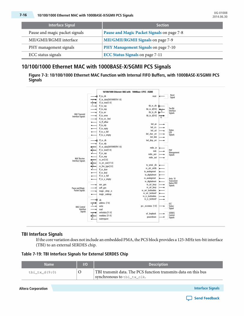
SectionInterface Signal
Pause and Magic Packet Signals on page 7-8Pause and magic packet signals
MII/GMII/RGMII Signals on page 7-9MII/GMII/RGMII interface
PHY Management Signals on page 7-10PHY management signals
ECC Status Signals on page 7-11ECC status signals
10/100/1000 Ethernet MAC with 1000BASE-X/SGMII PCS SignalsFigure 7-3: 10/100/1000 Ethernet MAC Function with Internal FIFO Buffers, with 1000BASE-X/SGMII PCSSignals
10/100/1000 Ethernet MAC with 1000Base -X PCS /SGMIIResetSignalreset
StatusLEDSignals
led_anled_crsled_col
led_char _errled_link
led_disp _err
PHYManagementSignals
mdio_inmdc
mdio_oenmdio_out
SERDESControlSignals
sd_loopbackpowerdown
Pause and MagicPacket Signals
xon_genxoff_gen
magic _wakeupmagic _sleep _n
n
2
MAC TransmitInterface Signals
ff_tx_crc _fwd
ff_tx_eopff_tx_err
ff_tx_sop
ff_tx_wren
tx_ff_uflow
ff_tx_clk
ff_tx_rdyff_tx_septy
ff_tx_mod[1:0]
ff_tx_a_fullff_tx_a_empty
n
2
6
18
4
MAC ReceiveInterface Signals
ff_rx_mod[1:0]
ff_rx_eopff_rx_sop
rx_err [5:0]rx_err_stat[17 :0]rx_frm_type[3:0]ff_rx_dsav
ff_rx_rdyff_rx_clk
ff_rx_dvalff_rx_a_fullff_rx_a_empty
8
32
32
MAC ControlInterfaceSignals
clkaddress [7:0]
readwrite
readdata [31 :0]writedata [31 :0]
waitrequest
Ten BitInterfaceSignals
tbi_rx_clktbi_rx_d[9:0]
tbi_tx_clktbi_tx_d[9:0]
10
10
ECCStatusSignal
pcs _eccstatus [1:0]
Arria 10TransceiverNative PHYSignals
tx_serial _clkrx_cdr_refclk
tx_analogresettx_digitalreset
rx_analogresetrx_digitalreset
tx_cal _busyrx_cal _busy
rx_set_locktodatarx_set_locktorefrx_is_locktodata
rx_is_locktoref
ff_rx_data[DATAWIDTH-1:0]
ff_tx_data[DATAWIDTH-1:0]
TBI Interface SignalsIf the core variation does not include an embedded PMA, the PCS block provides a 125-MHz ten-bit interface(TBI) to an external SERDES chip.
Table 7-19: TBI Interface Signals for External SERDES Chip
DescriptionI/OName
TBI transmit data. The PCS function transmits data on this bussynchronous to tbi_tx_clk.
Otbi_tx_d(9:0)
Interface SignalsAltera Corporation
Send Feedback
UG-0100810/100/1000 Ethernet MAC with 1000BASE-X/SGMII PCS Signals7-16 2014.06.30

DescriptionI/OName
125-MHzTBI transmit clock from external SERDES, typically sourcedby the local reference clock oscillator.
Itbi_tx_clk
125-MHz TBI receive clock from external SERDES, typically sourcedby the line clock recovered from the encoded line stream.
Itbi_rx_clk
TBI receive data. This bus carries the data from the external SERDES.Synchronize the bus with tbi_rx_clk. The data can be arbitraryaligned.
Itbi_rx_d[9:0]
Status LED Control Signals
Table 7-20: Status LED Interface Signals
DescriptionI/OName
When asserted, this signal indicates a successful link synchronization.Oled_link
When asserted, this signal indicates some activities on the transmitand receive paths. When deasserted, it indicates no traffic on thepaths.
Oled_crs
When asserted, this signal indicates that a collision was detectedduring frame transmission. This signal is always deasserted when thePCS function operates in standard 1000BASE-X mode or in full-duplex mode when SGMII is enabled.
Oled_col
Auto-negotiation status. The PCS function asserts this signal whenan auto-negotiation completes.
Oled_an
10-bit character error. Asserted for one tbi_rx_clk cycle when anerroneous 10-bit character is detected.
Oled_char_err
10-bit running disparity error. Asserted for one tbi_rx_clk cyclewhen a disparity error is detected. A running disparity error indicatesthat more than the previous and perhaps the current received grouphad an error.
Oled_disp_err
SERDES Control Signals
Table 7-21: SERDES Control Signal
DescriptionI/OName
Power-down enable. Asserted when the PCS function is in power-downmode; deassertedwhen the PCS function is operating in normalmode. This signal is implemented only when an external SERDES isused.
Opowerdown
SERDESLoopbackControl. Assertedwhen the PCS function operatesin loopback mode. You can use this signal to configure an externalSERDES device to operate in loopback mode.
Osd_loopback
Altera CorporationInterface Signals
Send Feedback
7-17Status LED Control SignalsUG-010082014.06.30

Arria 10 Transceiver Native PHY Signals
Table 7-22: Arria 10 Transceiver Native PHY Signals
DescriptionI/OName
Serial clock input from the transceiver PLL. The frequency of this clockdepends on the data rate and clock division factor.
Itx_serial_clk
Reference clock input to the receive clock data recovery (CDR)circuitry.
Irx_cdr_refclk
Resets the analog transmit portion of the transceiver PHY.Itx_analogreset
Resets the digital transmit portion of the transceiver PHY.Itx_digitalreset
Resets the analog receive portion of the transceiver PHY.Irx_analogreset
Resets the digital receive portion of the transceiver PHY.Irx_digitalreset
When asserted, this signal indicates that the transmit channel is beingcalibrated.
Otx_cal_busy
When asserted, this signal indicates that the receive channel is beingcalibrated.
Orx_cal_busy
Force the receiver CDR to lock to the incoming data.Irx_set_locktodata
Force the receiver CDR to lock to the phase and frequency of the inputreference clock.
Irx_set_locktoref
When asserted, this signal indicates that the CDR PLL is locked to theincoming data rx_serial_data.
Orx_is_lockedtodata
When asserted, this signal indicates that the CDR PLL is locked to theincoming reference clock, rx_cdr_refclk.
Orx_is_lockedtoref
Related InformationArria 10 Transceiver PHY User GuideMore information about Gigabit Ethernet (GbE) and GbE with 1588, the connection guidelines for a PHYdesign, and how to implement GbE/GbE with 1588 in Arria 10 Transceivers
Interface SignalsAltera Corporation
Send Feedback
UG-01008Arria 10 Transceiver Native PHY Signals7-18 2014.06.30
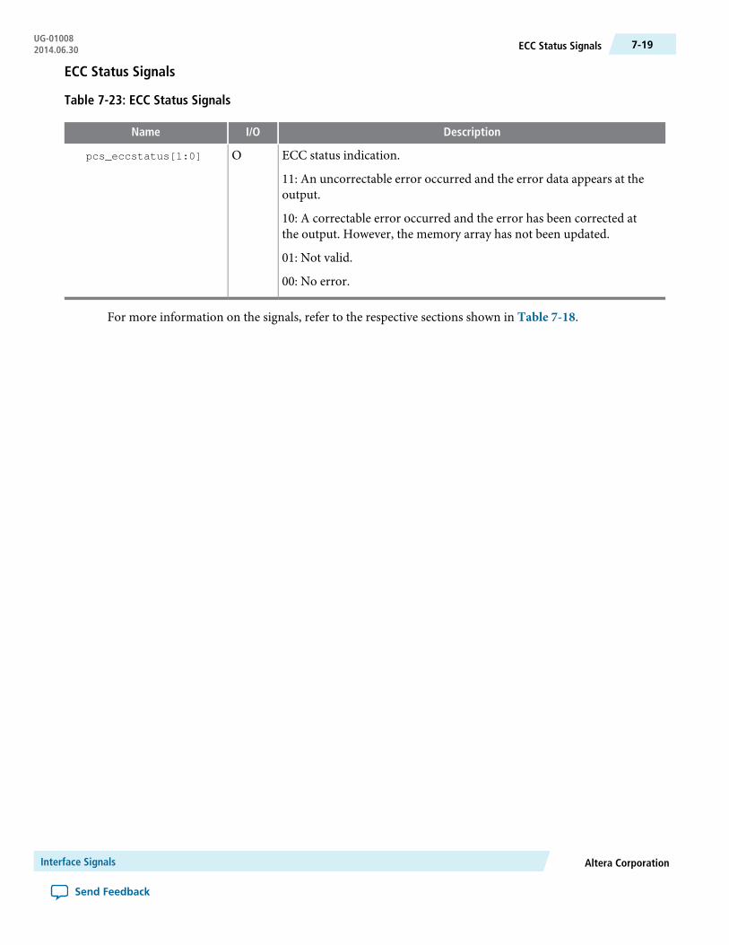
ECC Status Signals
Table 7-23: ECC Status Signals
DescriptionI/OName
ECC status indication.
11: An uncorrectable error occurred and the error data appears at theoutput.
10: A correctable error occurred and the error has been corrected atthe output. However, the memory array has not been updated.
01: Not valid.
00: No error.
Opcs_eccstatus[1:0]
For more information on the signals, refer to the respective sections shown in Table 7-18.
Altera CorporationInterface Signals
Send Feedback
7-19ECC Status SignalsUG-010082014.06.30

10/100/1000 Multiport Ethernet MAC with 1000BASE-X/SGMII PCS SignalsFigure 7-4: 10/100/1000 Multiport Ethernet MAC Function without Internal FIFO Buffers with1000BASE-X/SGMII PCS Signals
PHYManagementSignals
mdio_inmdc
mdio_oenmdio_out
ResetSignalreset
StatusLEDSignals
led_an_nled_crs _nled_col _n
led_char _err_nled_link_n
led_disp _err_n
SERDESControlSignals
sd _loopback _npowerdown _n
Pause and MagicPacket Signals
xon _gen _nxoff_gen _n
magic _wakeup _nmagic _sleep _n_n
8
5
mac _tx_clk_nmac _rx_clk_n
ClockSignals
data _rx_data _n[7:0]
data _rx_eop _ndata _rx_sop _n
data _rx_error _n[4:0]data _rx_ready _ndata _rx_valid _n
MAC ReceiveInterface Signals
MAC TransmitInterface Signals
data _tx_data _n[7:0]
data _tx_eop _ndata _tx_error _n
data _tx_sop _n
data _tx_valid _ndata _tx_ready _ntx_crc _fwd_ntx_ff_uflow_n
8
MAC PacketClassification
Signals
pkt_class _valid _npkt_class _data _n[4:0]
5
n rx_afull_data [1:0]rx_afull_valid
MAC FIFOStatus Signals
rx_afull_clk
Ten BitInterfaceSignals
tbi_rx_clk_ntbi_rx_d_n[9:0]
tbi_tx_clk_ntbi_tx_d_n[9:0]
10
10
32
32
MAC ControlInterfaceSignals
clk
reg_rdreg_wr
reg_data _out[31 :0]reg_data _in[31 :0]
reg_busy
8
rx_afull_channel[CHANNEL_WIDTH-1:0]
reg_addr[(log2 MAX_CHANNELS+7):0][7:0]
ECC StatusSignalpcs_eccstatus[1:0]
Multi-Port MAC with 1000BASE-X/SGMII PCS
Table 7-24: References
SectionInterface Signal
Clock and Reset Signal on page 7-2Clock and reset signals
MAC Control Interface Signals on page 7-3MAC control interface
MAC Transmit Interface Signals on page 7-6MAC transmit interface
MAC Receive Interface Signals on page 7-4MAC receive interface
Multiport MAC Packet Classification Signals on page 7-14MAC packet classification signals
Interface SignalsAltera Corporation
Send Feedback
UG-0100810/100/1000 Multiport Ethernet MAC with 1000BASE-X/SGMII PCS Signals7-20 2014.06.30

SectionInterface Signal
Multiport MAC FIFO Status Signals on page 7-15MAC FIFO status signals
Pause and Magic Packet Signals on page 7-8Pause and magic packet signals
PHY Management Signals on page 7-10PHY management signals
TBI Interface Signals on page 7-16Ten-bit interface
Status LED Control Signals on page 7-17Status LED signals
SERDES Control Signals on page 7-17SERDES control signals
Altera CorporationInterface Signals
Send Feedback
7-2110/100/1000 Multiport Ethernet MAC with 1000BASE-X/SGMII PCS SignalsUG-010082014.06.30
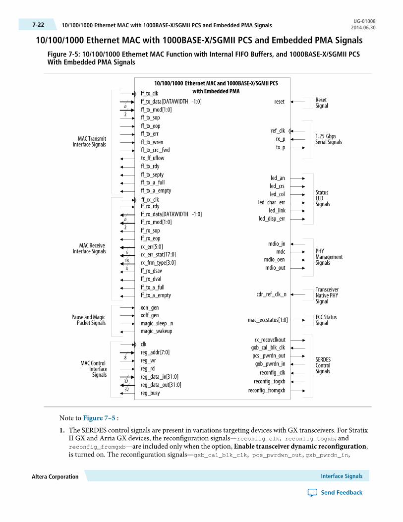
10/100/1000 Ethernet MAC with 1000BASE-X/SGMII PCS and Embedded PMA SignalsFigure 7-5: 10/100/1000 Ethernet MAC Function with Internal FIFO Buffers, and 1000BASE-X/SGMII PCSWith Embedded PMA Signals
StatusLEDSignals
led_anled_crsled_col
led_char_errled_link
led_disp_err
PHYManagementSignals
mdio_inmdc
mdio_oenmdio_out
1.25 GbpsSerial Signals
ref_clkrx_ptx_p
ResetSignal
reset
ECC StatusSignalmac_eccstatus[1:0]
TransceiverNative PHYSignal
cdr_ref_clk_n
Pause andMagicPacket Signals
xon_genxoff_gen
magic_wakeupmagic_sleep _n
n
2
MAC TransmitInterface Signals
ff_tx_crc_fwd
ff_tx_data[DATAWIDTH -1:0]
ff_tx_eopff_tx_err
ff_tx_sop
ff_tx_wren
tx_ff_uflowff_tx_rdyff_tx_septy
ff_tx_mod[1:0]
ff_tx_a_fullff_tx_a_empty
ff_tx_clk
ff_rx_clk
MAC ReceiveInterface Signals
ff_rx_data[DATAWIDTH -1:0]ff_rx_mod[1:0]
ff_rx_eopff_rx_sop
rx_err[5:0]rx_err_stat[17:0]rx_frm_type[3:0]ff_rx_dsav
ff_rx_rdy
ff_rx_dvalff_tx_a_fullff_tx_a_empty
n
2
6
18
4
SERDESControlSignals
pcs _pwrdn_outgxb_pwrdn_in
gxb_cal_blk_clk
reconfig_clkreconfig_togxb
reconfig_fromgxb
rx_recovclkout
32
32
MAC ControlInterfaceSignals
clkreg_addr[7:0]
reg_rdreg_wr
reg_data_out[31:0]reg_data_in[31:0]
reg_busy
8
10/100/1000 Ethernet MAC and 1000BASE-X/SGMII PCSwith Embedded PMA
Note to Figure 7–5 :
1. The SERDES control signals are present in variations targeting devices with GX transceivers. For StratixII GX and Arria GX devices, the reconfiguration signals—reconfig_clk, reconfig_togxb, andreconfig_fromgxb—are included only when the option, Enable transceiver dynamic reconfiguration,is turned on. The reconfiguration signals—gxb_cal_blk_clk, pcs_pwrdwn_out, gxb_pwrdn_in,
Interface SignalsAltera Corporation
Send Feedback
UG-0100810/100/1000 Ethernet MAC with 1000BASE-X/SGMII PCS and Embedded PMA Signals7-22 2014.06.30
reconfig_clk, and reconfig_busy—are not present in variations targeting Stratix V devices with GXtransceivers.
1.25 Gbps Serial InterfaceIf the variant includes an embedded PMA, the PMA provides a 1.25-GHz serial interface.
Table 7-25: 1.25 Gbps MDI Interface Signals
DescriptionI/OName
125 MHz local reference clock oscillator.Iref_clk
Serial Differential Receive Interface.Irx_p
Serial Differential Transmit Interface.Otx_p
Transceiver Native PHY Signal
Table 7-26: Transceiver Native PHY Signal
DescriptionI/OName
Port to connect the RX PLL reference clock with a frequency of 125MHz when you enable SyncE support.
Icdr_ref_clk_n
SERDES Control SignalsThese signals apply only to PMA blocks implemented in devices with GX transceivers.
Table 7-27: SERDES Control Signal
DescriptionI/OName
Recovered clock from the PMA block.Orx_recovclkout
Power-down status. Asserted when the PCS function is in power-downmode; deassertedwhen thePCS function is operating in normalmode. This signal is implemented only when an internal SERDES isused with the option to export the power-down signal.
This signal is not present in PMA blocks implemented in Stratix Vdevices with GX transceivers.
Opcs_pwrdn_out
Power-down enable. Assert this signal to power down the transceiverquad block. This signal is implemented only when an internalSERDES is used with the option to export the power-down signal.
This signal is not present in PMA blocks implemented in Stratix Vdevices with GX transceivers.
Igxb_pwrdn_in
Calibration block clock for the ALT2GXB module (SERDES). Thisclock is typically tied to the 125 MHz ref_clk. Only implementedwhen an internal SERDES is used.
This signal is not present in PMA blocks implemented in Stratix Vdevices with GX transceivers.
Igxb_cal_blk_clk
Altera CorporationInterface Signals
Send Feedback
7-231.25 Gbps Serial InterfaceUG-010082014.06.30

DescriptionI/OName
Reference clock for the dynamic reconfiguration controller. If youuse a dynamic reconfiguration controller in your design todynamically control the transceiver, both the reconfigurationcontroller and the MegaCore function require this clock. This clockmust operate between 37.5–50 MHz. Tie this clock low if you arenot using an external reconfiguration controller.
This signal is not present in PMA blocks implemented in Stratix Vdevices with GX transceivers.
Ireconfig_clk
Driven from an external dynamic reconfiguration controller.Supports the selection of multiple transceiver channels for dynamicreconfiguration.
For PMA blocks implemented in Stratix V devices with GXtransceivers, the bus width is [139:0]. For more information aboutthe bus width for PMA blocks implemented in each device, refer tothe Dynamic Reconfiguration chapter of the respective devicehandbook.
Ireconfig_togxb[n:0]
Connects to an external dynamic reconfiguration controller. Thebus identifies the transceiver channel whose settings are beingtransmitted to the reconfiguration controller. Leave this busdisconnected if you are not using an external reconfigurationcontroller.
For more information about the bus width for PMA blocksimplemented in each device, refer to the Dynamic Reconfigurationchapter of the respective device handbook.
Oreconfig_fromgxb[n:0]
Driven from an external dynamic reconfiguration controller. Thissignal will indicate the busy status of the dynamic reconfigurationcontroller during offset cancellation. Tie this signal to 1'b0 if you arenot using an external reconfiguration controller.
This signal is not present in PMA blocks implemented in Stratix Vdevices with GX transceivers.
Ireconfig_busy
For more information on the signals, refer to the respective sections shown in Table 7-24.
Interface SignalsAltera Corporation
Send Feedback
UG-01008SERDES Control Signals7-24 2014.06.30

10/100/1000 Multiport Ethernet MAC with 1000BASE-X/SGMII PCS and Embedded PMAFigure 7-6: 10/100/1000 Multiport Ethernet MAC Function without Internal FIFO Buffers, with IEEE 1588v2,1000BASE-X/SGMII PCS and Embedded PMA Signals
PHYManagementSignals
mdio_inmdc
mdio_oenmdio_out
ResetSignalreset
TransceiverNative PHY
Signalcdr_ref_clk_n
ECC StatusSignal
pcs_eccstatus[1:0]
1.25 GbpsSerial Signals
ref_clk_nrx_p_ntx_p_n
StatusLEDSignals
led_an_nled_crs_nled_col_n
led_char_err_nled_link_n
led_disp_err_n
mac_tx_clk_nmac_rx_clk_n
ClockSignals
xon_gen_nxoff_gen_n
magic_wakeup_nmagic_sleep_n_n
Pause and MagicPacket Signals
SERDESControlSignals
IEEE 1588v2Signals
pcs_pwrdn_outgxb_pwrdn_in_n
gxb_cal_blk_clk
reconfig_clk_nreconfig_togxb_n
8data_tx_data_n[7:0]
data_tx_eop_ndata_tx_error_n
data_tx_sop_n
data_tx_valid_ndata_tx_ready_n
MAC TransmitInterfaceSignals
tx_crc_fwd_ntx_ff_uflow_n
8
5
data_rx_data_n[7:0]
data_rx_eop_ndata_rx_sop_n
data_rx_error_n[4:0]data_rx_ready_ndata_rx_valid_n
MAC ReceiveInterfaceSignals
MAC PacketClassification
Signalspkt_class_valid_n
5
n rx_afull_data[1:0]rx_afull_valid
MAC FIFOStatus Signals
rx_afull_clk
32
n
clk
reg_rdreg_wr
reg_data_in[31:0]
reg_busyreg_data_out[31:0]
reg_addr[(log2 MAX_CHANNELS+7):0]
32
MAC ControlInterface Signals rx_recovclkout
reconfig_busy
reconfig_fromgxb_n
tx_egress_timestamp_96b_n
tx_time_of_day_96b_ntx_time_of_day_64b_nrx_time_of_day_96b_nrx_time_of_day_64b_npcs_phase_measure_clk
tx_egress_timestamp_request_ntx_etstamp_ins_ctrl_n
tx_egress_timestamp_64b_nrx_ingress_timestamp_96b_nrx_ingress_timestamp_64b_n
Multi-Port MAC and 1000BASE-X/SGMII PCSwith Embedded PMA
pkt_class_data_n[4:0]
rx_afull_channel(CHANNEL_WIDTH-1:0)
Note to Figure 7–6 :
1. The SERDES control signals are present in variations targeting devices with GX transceivers. For StratixII GX and Arria GX devices, the reconfiguration signals—reconfig_clk, reconfig_togxb, andreconfig_fromgxb—are included only when the Enable transceiver dynamic reconfiguration option isturned on. The reconfiguration signals—gxb_cal_blk_clk, pcs_pwrdwn_out, gxb_pwrdn_in,reconfig_clk, and reconfig_busy—are not present in variations targeting Stratix V devices with GXtransceivers.
Altera CorporationInterface Signals
Send Feedback
7-2510/100/1000 Multiport Ethernet MAC with 1000BASE-X/SGMII PCS and Embedded PMAUG-010082014.06.30
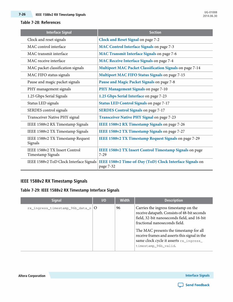
Table 7-28: References
SectionInterface Signal
Clock and Reset Signal on page 7-2Clock and reset signals
MAC Control Interface Signals on page 7-3MAC control interface
MAC Transmit Interface Signals on page 7-6MAC transmit interface
MAC Receive Interface Signals on page 7-4MAC receive interface
Multiport MAC Packet Classification Signals on page 7-14MAC packet classification signals
Multiport MAC FIFO Status Signals on page 7-15MAC FIFO status signals
Pause and Magic Packet Signals on page 7-8Pause and magic packet signals
PHY Management Signals on page 7-10PHY management signals
1.25 Gbps Serial Interface on page 7-231.25 Gbps Serial Signals
Status LED Control Signals on page 7-17Status LED signals
SERDES Control Signals on page 7-17SERDES control signals
Transceiver Native PHY Signal on page 7-23Transceiver Native PHY signal
IEEE 1588v2 RX Timestamp Signals on page 7-26IEEE 1588v2 RX Timestamp Signals
IEEE 1588v2 TX Timestamp Signals on page 7-27IEEE 1588v2 TX Timestamp Signals
IEEE 1588v2 TX Timestamp Request Signals on page 7-29IEEE 1588v2 TX Timestamp RequestSignals
IEEE 1588v2 TX Insert Control Timestamp Signals on page7-29
IEEE 1588v2 TX Insert ControlTimestamp Signals
IEEE 1588v2 Time-of-Day (ToD) Clock Interface Signals onpage 7-32
IEEE 1588v2 ToD Clock Interface Signals
IEEE 1588v2 RX Timestamp Signals
Table 7-29: IEEE 1588v2 RX Timestamp Interface Signals
DescriptionWidthI/OSignal
Carries the ingress timestamp on thereceive datapath. Consists of 48-bit secondsfield, 32-bit nanoseconds field, and 16-bitfractional nanoseconds field.
The MAC presents the timestamp for allreceive frames and asserts this signal in thesame clock cycle it asserts rx_ingress_timestamp_96b_valid.
96Orx_ingress_timestamp_96b_data_n
Interface SignalsAltera Corporation
Send Feedback
UG-01008IEEE 1588v2 RX Timestamp Signals7-26 2014.06.30

DescriptionWidthI/OSignal
When asserted, this signal indicates thatrx_ingress_timestamp_96b_data
contains valid timestamp.
For all receive frame, the MAC asserts thissignal in the same clock cycle it receivesthe start of packet (avalon_st_rx_startofpacket is asserted).
1Orx_ingress_timestamp_96b_valid
Carries the ingress timestamp on thereceive datapath. Consists of 48-bitnanoseconds field and 16-bit fractionalnanoseconds field.
The MAC presents the timestamp for allreceive frames and asserts this signal in thesame clock cycle it asserts rx_ingress_timestamp_64b_valid.
64Orx_ingress_timestamp_64b_data
When asserted, this signal indicates thatrx_ingress_timestamp_64b_data
contains valid timestamp.
For all receive frame, the MAC asserts thissignal in the same clock cycle it receivesthe start of packet (avalon_st_rx_startofpacket is asserted).
1Orx_ingress_timestamp_64b_valid
IEEE 1588v2 TX Timestamp Signals
Table 7-30: IEEE 1588v2 TX Timestamp Interface Signals
DescriptionWidthI/OSignal
A transmit interface signal. This signalrequests timestamp of frames on the TXpath. The timestamp is used to calculatethe residence time.
Consists of 48-bit seconds field, 32-bitnanoseconds field, and 16-bit fractionalnanoseconds field.
96Otx_egress_timestamp_96b_data_n
Altera CorporationInterface Signals
Send Feedback
7-27IEEE 1588v2 TX Timestamp SignalsUG-010082014.06.30
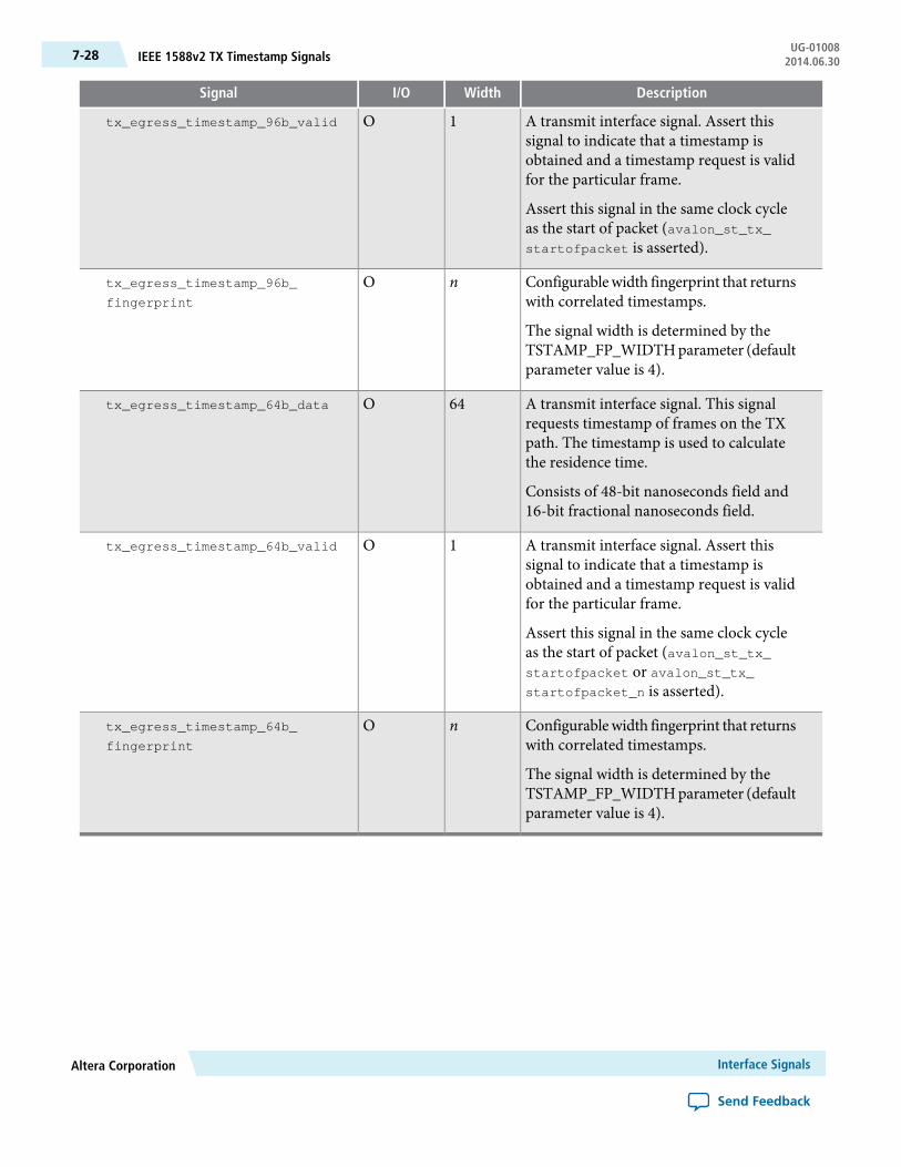
DescriptionWidthI/OSignal
A transmit interface signal. Assert thissignal to indicate that a timestamp isobtained and a timestamp request is validfor the particular frame.
Assert this signal in the same clock cycleas the start of packet (avalon_st_tx_startofpacket is asserted).
1Otx_egress_timestamp_96b_valid
Configurablewidth fingerprint that returnswith correlated timestamps.
The signal width is determined by theTSTAMP_FP_WIDTHparameter (defaultparameter value is 4).
nOtx_egress_timestamp_96b_
fingerprint
A transmit interface signal. This signalrequests timestamp of frames on the TXpath. The timestamp is used to calculatethe residence time.
Consists of 48-bit nanoseconds field and16-bit fractional nanoseconds field.
64Otx_egress_timestamp_64b_data
A transmit interface signal. Assert thissignal to indicate that a timestamp isobtained and a timestamp request is validfor the particular frame.
Assert this signal in the same clock cycleas the start of packet (avalon_st_tx_startofpacket or avalon_st_tx_startofpacket_n is asserted).
1Otx_egress_timestamp_64b_valid
Configurablewidth fingerprint that returnswith correlated timestamps.
The signal width is determined by theTSTAMP_FP_WIDTHparameter (defaultparameter value is 4).
nOtx_egress_timestamp_64b_
fingerprint
Interface SignalsAltera Corporation
Send Feedback
UG-01008IEEE 1588v2 TX Timestamp Signals7-28 2014.06.30
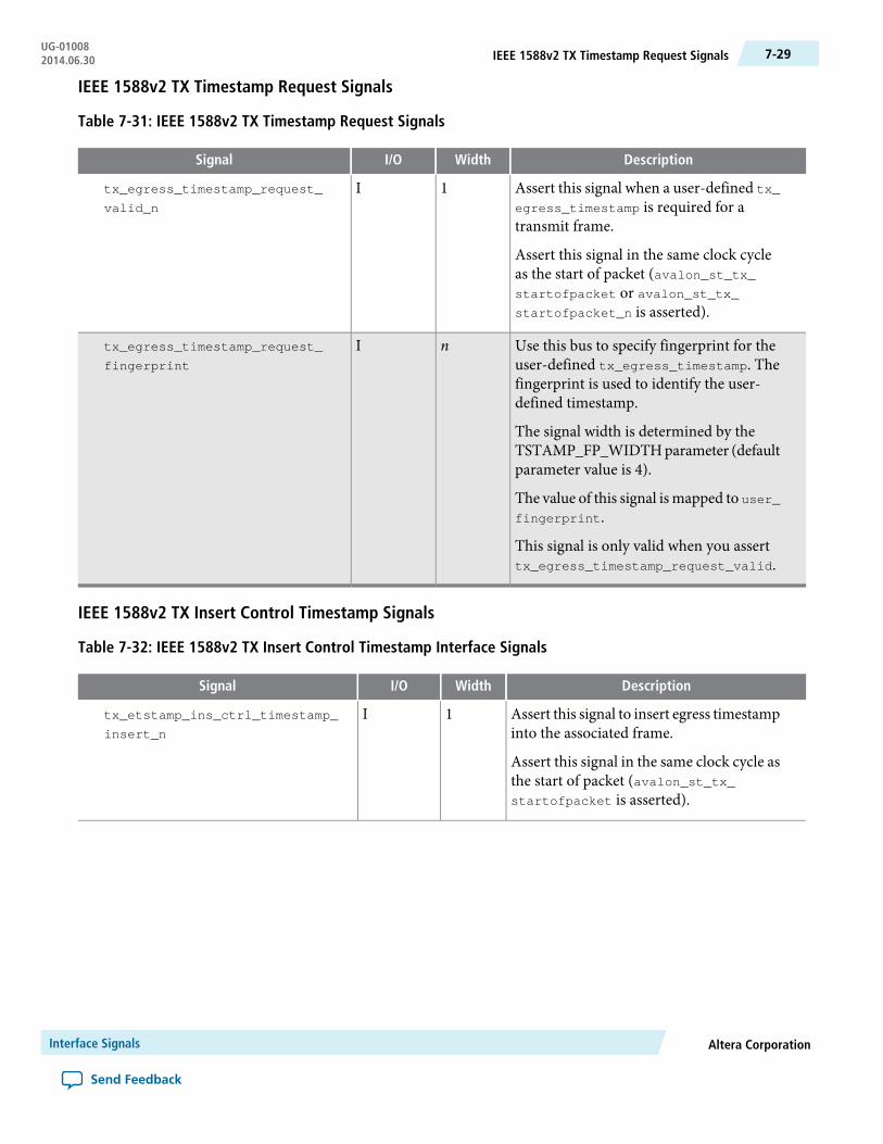
IEEE 1588v2 TX Timestamp Request Signals
Table 7-31: IEEE 1588v2 TX Timestamp Request Signals
DescriptionWidthI/OSignal
Assert this signal when a user-defined tx_
egress_timestamp is required for atransmit frame.
Assert this signal in the same clock cycleas the start of packet (avalon_st_tx_startofpacket or avalon_st_tx_startofpacket_n is asserted).
1Itx_egress_timestamp_request_
valid_n
Use this bus to specify fingerprint for theuser-defined tx_egress_timestamp. Thefingerprint is used to identify the user-defined timestamp.
The signal width is determined by theTSTAMP_FP_WIDTHparameter (defaultparameter value is 4).
The value of this signal ismapped to user_fingerprint.
This signal is only valid when you asserttx_egress_timestamp_request_valid.
nItx_egress_timestamp_request_
fingerprint
IEEE 1588v2 TX Insert Control Timestamp Signals
Table 7-32: IEEE 1588v2 TX Insert Control Timestamp Interface Signals
DescriptionWidthI/OSignal
Assert this signal to insert egress timestampinto the associated frame.
Assert this signal in the same clock cycle asthe start of packet (avalon_st_tx_startofpacket is asserted).
1Itx_etstamp_ins_ctrl_timestamp_
insert_n
Altera CorporationInterface Signals
Send Feedback
7-29IEEE 1588v2 TX Timestamp Request SignalsUG-010082014.06.30
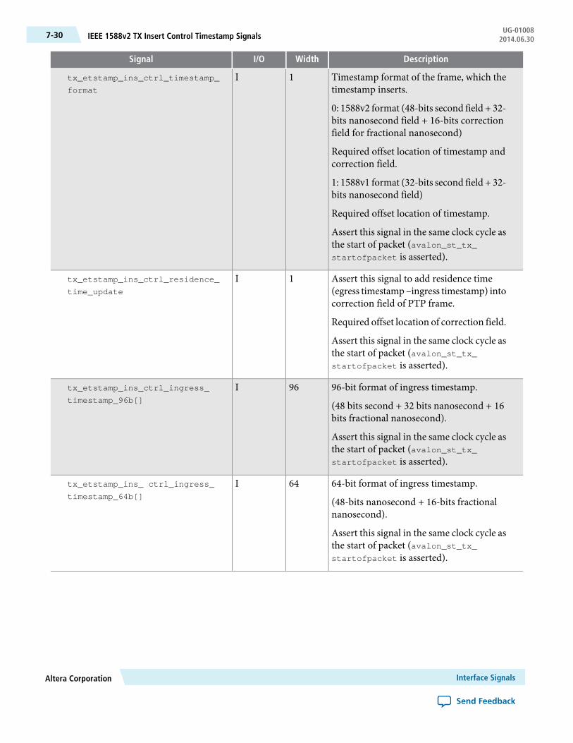
DescriptionWidthI/OSignal
Timestamp format of the frame, which thetimestamp inserts.
0: 1588v2 format (48-bits second field + 32-bits nanosecond field + 16-bits correctionfield for fractional nanosecond)
Required offset location of timestamp andcorrection field.
1: 1588v1 format (32-bits second field + 32-bits nanosecond field)
Required offset location of timestamp.
Assert this signal in the same clock cycle asthe start of packet (avalon_st_tx_startofpacket is asserted).
1Itx_etstamp_ins_ctrl_timestamp_
format
Assert this signal to add residence time(egress timestamp –ingress timestamp) intocorrection field of PTP frame.
Required offset location of correction field.
Assert this signal in the same clock cycle asthe start of packet (avalon_st_tx_startofpacket is asserted).
1Itx_etstamp_ins_ctrl_residence_
time_update
96-bit format of ingress timestamp.
(48 bits second + 32 bits nanosecond + 16bits fractional nanosecond).
Assert this signal in the same clock cycle asthe start of packet (avalon_st_tx_startofpacket is asserted).
96Itx_etstamp_ins_ctrl_ingress_
timestamp_96b[]
64-bit format of ingress timestamp.
(48-bits nanosecond + 16-bits fractionalnanosecond).
Assert this signal in the same clock cycle asthe start of packet (avalon_st_tx_startofpacket is asserted).
64Itx_etstamp_ins_ ctrl_ingress_
timestamp_64b[]
Interface SignalsAltera Corporation
Send Feedback
UG-01008IEEE 1588v2 TX Insert Control Timestamp Signals7-30 2014.06.30

DescriptionWidthI/OSignal
Format of timestamp to be used forresidence time calculation.
0: 96-bits (96-bits egress timestamp - 96-bits ingress timestamp).
1: 64-bits (64-bits egress timestamp - 64-bits ingress timestamp).
Assert this signal in the same clock cycle asthe start of packet (avalon_st_tx_startofpacket is asserted).
1Itx_etstamp_ins_ctrl_residence_
time_calc_format
Assert this signal to set the checksum fieldof UDP/IPv4 to zero.
Required offset location of checksum field.
Assert this signal in the same clock cycle asthe start of packet (avalon_st_tx_startofpacket is asserted).
1Itx_etstamp_ins_ctrl_checksum_zero
Assert this signal to correct UDP/IPv6packet checksum, by updating thechecksum correction, which is specified bychecksum correction offset.
Required offset location of checksumcorrection.
Assert this signal in the same clock cycle asthe start of packet (avalon_st_tx_startofpacket is asserted).
1Itx_etstamp_ins_ctrl_checksum_
correct
The location of the timestamp field, relativeto the first byte of the packet.
Assert this signal in the same clock cycle asthe start of packet (avalon_st_tx_startofpacket is asserted).
1Itx_etstamp_ins_ctrl_offset_
timestamp
The location of the correction field, relativeto the first byte of the packet.
Assert this signal in the same clock cycle asthe start of packet (avalon_st_tx_startofpacket is asserted).
16Itx_etstamp_ins_ctrl_offset_
correction_field[]
Altera CorporationInterface Signals
Send Feedback
7-31IEEE 1588v2 TX Insert Control Timestamp SignalsUG-010082014.06.30

DescriptionWidthI/OSignal
The location of the checksum field, relativeto the first byte of the packet.
Assert this signal in the same clock cycle asthe start of packet (avalon_st_tx_startofpacket is asserted).
16Itx_etstamp_ins_ctrl_offset_
checksum_field[]
The location of the checksum correctionfield, relative to the first byte of the packet.
Assert this signal in the same clock cycle asthe start of packet (avalon_st_tx_startofpacket is asserted).
16Itx_etstamp_ins_ctrl_offset_
checksum_correction[]
IEEE 1588v2 Time-of-Day (ToD) Clock Interface Signals
Table 7-33: IEEE 1588v2 ToD Clock Interface Signals
DescriptionWidthI/OSignal
Use this bus to carry the time-of-day fromexternal ToD module to 96-bit MAC TXclock.
Consists of 48 bits seconds field, 32 bitsnanoseconds field, and 16 bits fractionalnanoseconds field
96Itx_time_of_day_96b_data_n
Use this bus to carry the time-of-day fromexternal ToD module to 96-bit MAC RXclock.
Consists of 48 bits seconds field, 32 bitsnanoseconds field, and 16 bits fractionalnanoseconds field
96Irx_time_of_day_96b_data
Use this bus to carry the time-of-day fromexternal ToD module to 64-bit MAC TXclock.
Consists of 48-bit nanoseconds field and16-bit fractional nanoseconds field
64Itx_time_of_day_64b_data
Use this bus to carry the time-of-day fromexternal ToD module to 64-bit MAC RXclock.
Consists of 48-bit nanoseconds field and16-bit fractional nanoseconds field
64Irx_time_of_day_64b_data
Interface SignalsAltera Corporation
Send Feedback
UG-01008IEEE 1588v2 Time-of-Day (ToD) Clock Interface Signals7-32 2014.06.30

IEEE 1588v2 PCS Phase Measurement Clock Signal
Table 7-34: IEEE 1588v2 PCS Phase Measurement Clock Signal
DescriptionWidthI/OSignal
Sampling clock to measure the latencythrough the PCS FIFO buffer. Therecommended frequency is 80 MHz.
1Ipcs_phase_measure_clk
IEEE 1588v2 PHY Path Delay Interface Signals
Table 7-35: IEEE 1588v2 PHY Path Delay Interface Signals
DescriptionWidthI/OSignal
Use this bus to carry the path delay on thetransmit datapath. The delay is measuredbetween the physical network and MII/GMII to adjust the egress timestamp.
Bits 0 to 9—Fractional number of clockcycles
Bits 10 to 21—Number of clock cycles
22Itx_path_delay_data
Use this bus to carry the path delay on thereceive datapath. The delay is measuredbetween the physical network and MII/GMII to adjust the ingress timestamp.
Bits 0 to 9—Fractional number of clockcycles
Bits 10 to 21—Number of clock cycles
22Irx_path_delay_data
Altera CorporationInterface Signals
Send Feedback
7-33IEEE 1588v2 PCS Phase Measurement Clock SignalUG-010082014.06.30

1000BASE-X/SGMII PCS SignalsFigure 7-7: 1000BASE-X/SGMII PCS Function Signals
ResetSignals
reset _rx_clk
reset _tx_clkreset _reg _clk
set _10set _100set _1000hd_ena
SGMIIStatus
Signals
StatusLEDSignals
led _anled _crs
led _colled _char _err
led _linkled _disp _err
SERDESControlSignals
sd _loopbackpowerdown
rx_clktx_clk
MII /GMIIClock
Signals
rx_clkenatx_clkena
ClockEnablerSignals
GMIISignals gmii _rx_d[7 :0]
gmii _rx_dvgmii _rx_err
gmii _tx_d[7 :0]gmii _tx_engmii _tx_err
8
8
mii_rx_d[3 :0]mii_rx_dvmii_rx_errmii_colmii_crs
mii_tx_d[3 :0]mii_tx_enmii_tx_err
MIISignals 4
4
PCSControlInterfaceSignals
reg _clkreg _addr [4 :0]
reg _rdreg _wr
reg _data _out [15 :0]reg _data _in[15 :0]
reg _busy
5
16
16
Ten BitInterfaceSignals
tbi_rx_clk
tbi_rx_d[9 :0]tbi_tx_clk
tbi_tx_d[9 :0]
10
10
Arria 10TransceiverNative PHYSignals
1000 BASE-X/SGMII PCS Function
tx_serial_clkrx_cdr_refclk
tx_analogresettx_digitalresetrx_analogresetrx_digitalreset
tx_cal_busyrx_cal_busy
rx_set_locktodatarx_set_locktorefrx_is_locktodatarx_is_locktoref
Note to Figure 7–7 :
1. The clock enabler signals are present only in SGMII mode.
Interface SignalsAltera Corporation
Send Feedback
UG-010081000BASE-X/SGMII PCS Signals7-34 2014.06.30
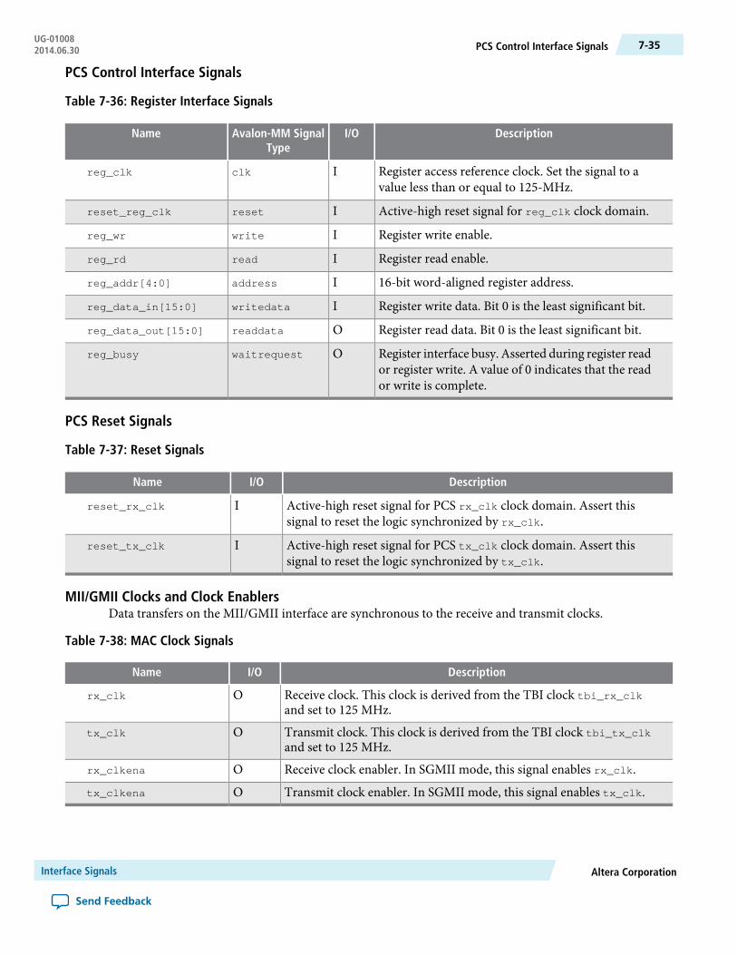
PCS Control Interface Signals
Table 7-36: Register Interface Signals
DescriptionI/OAvalon-MM SignalType
Name
Register access reference clock. Set the signal to avalue less than or equal to 125-MHz.
Iclkreg_clk
Active-high reset signal for reg_clk clock domain.Iresetreset_reg_clk
Register write enable.Iwritereg_wr
Register read enable.Ireadreg_rd
16-bit word-aligned register address.Iaddressreg_addr[4:0]
Register write data. Bit 0 is the least significant bit.Iwritedatareg_data_in[15:0]
Register read data. Bit 0 is the least significant bit.Oreaddatareg_data_out[15:0]
Register interface busy. Asserted during register reador register write. A value of 0 indicates that the reador write is complete.
Owaitrequestreg_busy
PCS Reset Signals
Table 7-37: Reset Signals
DescriptionI/OName
Active-high reset signal for PCS rx_clk clock domain. Assert thissignal to reset the logic synchronized by rx_clk.
Ireset_rx_clk
Active-high reset signal for PCS tx_clk clock domain. Assert thissignal to reset the logic synchronized by tx_clk.
Ireset_tx_clk
MII/GMII Clocks and Clock EnablersData transfers on the MII/GMII interface are synchronous to the receive and transmit clocks.
Table 7-38: MAC Clock Signals
DescriptionI/OName
Receive clock. This clock is derived from the TBI clock tbi_rx_clk
and set to 125 MHz.Orx_clk
Transmit clock. This clock is derived from the TBI clock tbi_tx_clk
and set to 125 MHz.Otx_clk
Receive clock enabler. In SGMII mode, this signal enables rx_clk.Orx_clkena
Transmit clock enabler. In SGMII mode, this signal enables tx_clk.Otx_clkena
Altera CorporationInterface Signals
Send Feedback
7-35PCS Control Interface SignalsUG-010082014.06.30

Figure 7-8: Clock Enabler Signal Behavior
125 MHz Clock
25 MHz Clock Enable
Input Data
Output Data
0xAA
0xAA
0xBB
0xBB
0xCC
0xCC
0xDD
0xDD
0xEE
GMII
Table 7-39: GMII Signals
DescriptionI/OName
GMII Transmit Interface
GMII transmit data bus.Igmii_tx_d[7:0]
Assert this signal to indicate that the data on gmii_tx_d[7:0]is valid.Igmii_tx_en
Assert this signal to indicate to the PHY device that the current framesent is invalid.
Igmii_tx_err
GMII Receive Interface
GMII receive data bus.Ogmii_rx_d[7:0]
Asserted to indicate that the data on gmii_rx_d[7:0] is valid. Staysasserted during frame reception, from the first preamble byte untilthe last byte in the CRC field is received.
Ogmii_rx_dv
Asserted by the PHY to indicate that the current frame contains errors.Ogmii_rx_err
MII
Table 7-40: MII Signals
DescriptionI/OName
MII Transmit Interface
MII transmit data bus.Imii_tx_d[3:0]
Assert this signal to indicate that the data on mii_tx_d[3:0]is valid.Imii_tx_en
Assert this signal to indicate to the PHY device that the frame sent isinvalid.
Imii_tx_err
MII Receive Interface
MII receive data bus.Omii_rx_d[3:0]
Asserted to indicate that the data on mii_rx_d[3:0]is valid. The signalstays asserted during frame reception, from the first preamble byteuntil the last byte of the CRC field is received.
Omii_rx_dv
Interface SignalsAltera Corporation
Send Feedback
UG-01008GMII7-36 2014.06.30

DescriptionI/OName
Asserted by the PHY to indicate that the current frame contains errors.Omii_rx_err
Collision detection. Asserted by the PCS function to indicate that acollision was detected during frame transmission.
Outmii_col
Carrier sense detection. Asserted by the PCS function to indicate thata transmit or receive activity is detected on the Ethernet line.
Outmii_crs
SGMII Status SignalsThe SGMII status signals provide status information to the PCS block. When the PCS is instantiatedstandalone, these signals are inputs to the MAC and serve as interface control signals for that block.
Table 7-41: SGMII Status Signals
DescriptionI/OName
Gigabit mode enabled. In 1000BASE-X, this signal is always set to 1.In SGMII, this signal is set to 1 if one of the following conditions ismet:
the USE_SGMII_AN bit is set to 1 and a gigabit link is established withthe link partner, as decoded from the partner_ability register
the USE_SGMII_AN bit is set to 0 and the SGMII_SPEED bit is set to 10
Oset_1000
100 -Mbps mode enabled. In 1000BASE-X, this signal is always set to0. In SGMII, this signal is set to 1 if one of the following conditions ismet:
the USE_SGMII_AN bit is set to 1 and a 100Mbps link is establishedwith the link partner, as decoded from the partner_ability register
the USE_SGMII_AN bit is set to 0 and the SGMII_SPEED bit is set to 01
Oset_100
10 -Mbps mode enabled. In 1000BASE-X, this signal is always set to0. In SGMII, this signal is set to 1 if one of the following conditions ismet:
the USE_SGMII_AN bit is set to 1 and a 10Mbps link is established withthe link partner, as decoded from the partner_ability register
the USE_SGMII_AN bit is set to 0 and the SGMII_SPEED bit is set to 00
Oset_10
Half-duplex mode enabled. In 1000BASE-X, this signal is always setto 0. In SGMII, this signal is set to 1 if one of the following conditionsis met:
the USE_SGMII_AN bit is set to 1 and a half-duplex link is establishedwith the link partner, as decoded from the partner_ability register
the USE_SGMII_AN bit is set to 0 and the SGMII_DUPLEX bit is set to 1
Ohd_ena
Altera CorporationInterface Signals
Send Feedback
7-37SGMII Status SignalsUG-010082014.06.30
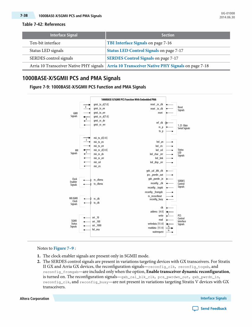
Table 7-42: References
SectionInterface Signal
TBI Interface Signals on page 7-16Ten-bit interface
Status LED Control Signals on page 7-17Status LED signals
SERDES Control Signals on page 7-17SERDES control signals
Arria 10 Transceiver Native PHY Signals on page 7-18Arria 10 Transceiver Native PHY signals
1000BASE-X/SGMII PCS and PMA SignalsFigure 7-9: 1000BASE-X/SGMII PCS Function and PMA Signals
ResetSignals
reset _rx_clkreset _tx_clk
reset
set _10set _100set _1000hd_ena
SGMIIStatus
Signals
StatusLEDSignals
led_anled_crsled_col
led_char _errled_link
led_disp _err
led_an
rx_clktx_clk
MII /GMIIClock
Signals
rx_clkenatx_clkena
ClockEnablerSignals
GMIISignals gmii_rx_d[7:0]
gmii_rx_dvgmii_rx_err
gmii_tx_d[7:0]gmii_tx_engmii_tx_err
8
8
mii_rx_d[3:0]mii_rx_dvmii_rx_errmii_colmii_crs
mii_tx_d[3:0]mii_tx_enmii_tx_err
MIISignals
4
4
PCSControlInterfaceSignals
clkaddress [4:0]
readwrite
readdata [15 :0]writedata [15 :0]
waitrequest 16
16
5
SERDESControlSignals
pcs _pwrdn _outgxb _pwrdn _in
gxb _cal _blk_clk
reconfig _clkreconfig _togxb
reconfig _fromgxbrx_recovclkout
1.25 GbpsSerial Signals
ref_clkrx_ptx_p
reconfig_busy
1000BASE-X/SGMII PCS Function With Embedded PMA
Notes to Figure 7–9 :
1. The clock enabler signals are present only in SGMII mode.2. The SERDES control signals are present in variations targeting devices with GX transceivers. For Stratix
II GX and Arria GX devices, the reconfiguration signals—reconfig_clk, reconfig_togxb, andreconfig_fromgxb—are included only when the option, Enable transceiver dynamic reconfiguration,is turned on. The reconfiguration signals—gxb_cal_blk_clk, pcs_pwrdwn_out, gxb_pwrdn_in,reconfig_clk, and reconfig_busy—are not present in variations targeting Stratix V devices with GXtransceivers.
Interface SignalsAltera Corporation
Send Feedback
UG-010081000BASE-X/SGMII PCS and PMA Signals7-38 2014.06.30

Table 7-43: References
SectionInterface Signal
PCS Reset Signals on page 7-35Reset signals
MII/GMII Clocks and Clock Enablers on page 7-35MII/GMII clocks and clock enablers
PCS Control Interface Signals on page 7-35PCS control interface
GMII on page 7-36GMII signals
MII on page 7-36MII signals
SGMII Status Signals on page 7-37SGMII status signals
1.25 Gbps Serial Interface on page 7-231.25 Gbps Serial Signals
Status LED Control Signals on page 7-17Status LED signals
SERDES Control Signals on page 7-17SERDES control signals
Transceiver Native PHY Signal on page 7-23Transceiver Native PHY signal
TimingThis section shows the timing on the Triple-Speed Ethernet transmit and receive interfaces as well as thetimestamp signals for the IEEE 1588v2 feature.
Related InformationAvalon Interface SpecificationsMore information on Avalon-MM control interface timing
Avalon-ST Receive InterfaceFigure 7-10: Receive Operation—MAC With Internal FIFO Buffers
ff_rx_clk
ff_rx_data[31:0]
ff_rx_sop
ff_rx_eop
ff_rx_rdy
ff_rx_dval
ff_rx_dsav
rx_frm_type[3:0]
rx_err_stat[17:0]
rx_err[5:0]
ff_rx_mod[1:0]
0000000000000000 00000000 00000001 00000002 00000003 00000004 00000005 00000000
00 1 0
0000000000 00064 00000
00
0
Altera CorporationInterface Signals
Send Feedback
7-39TimingUG-010082014.06.30
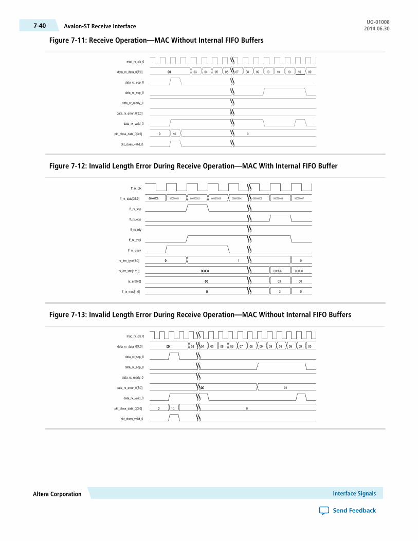
Figure 7-11: Receive Operation—MAC Without Internal FIFO Buffers
mac_rx_clk_0
data_rx_data_0[7:0]
data_rx_sop_0
data_rx_eop_0
data_rx_ready_0
data_rx_error_0[5:0]
data_rx_valid_0
pkt_class_data_0[3:0]
pkt_class_valid_0
0000 03 04 05 06 07 08 09 10 10 10 10 00
00
00 10 0
Figure 7-12: Invalid Length Error During Receive Operation—MAC With Internal FIFO Buffer
ff_rx_clk
ff_rx_data[31:0]
ff_rx_sop
ff_rx_eop
ff_rx_rdy
ff_rx_dval
ff_rx_dsav
rx_frm_type[3:0]
rx_err_stat[17:0]
rx_err[5:0]
ff_rx_mod[1:0]
0000000000000000 00000001 00000002 00000003 00000004 00000005 00000006 00000007
00 1 0
0000000000 005DD 00000
0000 03 00
00 3 0
Figure 7-13: Invalid Length Error During Receive Operation—MAC Without Internal FIFO Buffers
mac_rx_clk_0
data_rx_data_0[7:0]
data_rx_sop_0
data_rx_eop_0
data_rx_ready_0
data_rx_error_0[5:0]
data_rx_valid_0
pkt_class_data_0[3:0]
pkt_class_valid_0
0000 03 04 05 06 06 07 08 09 09 09 09 09 00
0000 01
00 10 0
Interface SignalsAltera Corporation
Send Feedback
UG-01008Avalon-ST Receive Interface7-40 2014.06.30

Avalon-ST Transmit InterfaceFigure 7-14: Transmit Operation—MAC With Internal FIFO Buffers
ff_tx_clk
ff_tx_data[31:0]
ff_tx_sop
ff_tx_eop
ff_tx_rdy
ff_tx_wren
ff_tx_crc_fwd
ff_tx_err
ff_tx_mod[1:0]
ff_tx_septy
tx_ff_uflow
00000001 00000002 00000003 00000004 00000005 00000006
Figure 7-15: Transmit Operation—MAC Without Internal FIFO Buffers
mac_tx_clk_0
data_tx_data_0[7:0]
data_tx_sop_0
data_tx_eop_0
data_tx_ready_0
data_tx_err_0
data_tx_valid_0
0000 01 01 01 02 03 04 05 06 07 08 09
GMII TransmitOn transmit, all data transfers are synchronous to the rising edge of tx_clk. The GMII data enable signalgm_tx_en is asserted to indicate the start of a new frame and remains asserted until the last byte of the frameis present on gm_tx_d[7:0] bus. Between frames, gm_tx_en remains deasserted.
If a frame is received on the Avalon-ST interface with an error (asserted with ff_tx_eop), the frame issubsequently transmitted with the GMII gm_tx_err error signal at any time during the frame transfer.
GMII ReceiveOn receive, all signals are sampled on the rising edge of rx_clk. The GMII data enable signal gm_rx_dv isasserted by the PHY to indicate the start of a new frame and remains asserted until the last byte of the frameis present on the gm_rx_d[7:0] bus. Between frames, gm_rx_dv remains deasserted.
If the PHY detects an error on the frame received from the line, the PHY asserts the GMII error signal,gm_rx_err, for at least one clock cycle at any time during the frame transfer.
A frame received on the GMII interface with a PHY error indication is subsequently transferred on theAvalon-ST interface with the error signal rx_err[0] asserted.
Altera CorporationInterface Signals
Send Feedback
7-41Avalon-ST Transmit InterfaceUG-010082014.06.30

RGMII TransmitOn transmit, all data transfers are synchronous to both edges of tx_clk. TheRGMII control signal tx_controlis asserted to indicate the start of a new frame and remains asserted until the last upper nibble of the frameis present on the rgmii_out[3:0] bus. Between frames, tx_control remains deasserted.
Figure 7-16: RGMII Transmit in 10/100 Mbps
tx_clk
tx_control
rgmii_out[3:0] 00 5 D 0 5 1 6 1 9 1
Figure 7-17: RGMII Transmit in Gigabit Mode
tx_clk
tx_control
rgmii_out[3:0] 00 5 D 0 5 4 5 E 5 F 5 0 6 0
If a frame is received on the Avalon-ST interface with an error (ff_tx_err asserted with ff_tx_eop), theframe is subsequently transmitted with the RGMII tx_control error signal (at the falling edge of tx_clk)at any time during the frame transfer.
Figure 7-18: RGMII Transmit with Error in 1000 Mbps
tx_clk
tx_control
rgmii_out[3:0] 00 5 0 4 6 0 1 0 0 8 0 9 0
RGMII ReceiveOn receive all signals are sampled on both edges of rx_clk. The RGMII control signal rx_control is assertedby the PHY to indicate the start of a new frame and remains asserted until the last upper nibble of the frameis present on rgmii_in[3:0] bus. Between frames, rx_control remains deasserted.
Figure 7-19: RGMII Receive in 10/100 Mbps
rx_clk
rx_control
rgmii_in[3:0] 00 5 D 0 5 1 6 1 9 0
Interface SignalsAltera Corporation
Send Feedback
UG-01008RGMII Transmit7-42 2014.06.30

Figure 7-20: RGMII Receive in 1000 Mbps
rx_clk
rx_control
rgmii_in[3:0] 00 5 D 0 5 4 5 E 5 F 5 0 6 0
A frame received on the RGMII interface with a PHY error indication is subsequently transferred on theAvalon-ST interface with the error signal rx_err[0]asserted.
Figure 7-21: RGMII Receive with Error in Gigabit Mode
rx_clk
rx_control
rgmii_in[3:0] 00 5 0 4 6 0 1 0 0 8 0 9 0
The current implementation of the RGMII receive interface expects a positive-delay rx_clk relative to thereceive data (the clock comes after the data).
MII TransmitOn transmit, all data transfers are synchronous to the rising edge of tx_clk. The MII data enable signal,m_tx_en, is asserted to indicate the start of a new frame and remains asserted until the last byte of the frameis present on m_tx_d[3:0] bus. Between frames, m_tx_en remains deasserted.
If a frame is received on the FIFO interface with an error (ff_tx_err asserted) the frame is subsequentlytransmitted with the MII error signal m_tx_err for one clock cycle at any time during the frame transfer.
MII ReceiveOn receive, all signals are sampled on the rising edge of rx_clk. The MII data enable signal m_rx_en isasserted by the PHY to indicate the start of a new frame and remains asserted until the last byte of the frameis present on m_rx_d[3:0] bus. Between frames, m_rx_en remains deasserted.
If the PHY detects an error on the frame received from the line, the PHY asserts the MII error signal,m_rx_err, for at least one clock cycle at any time during the frame transfer.
A frame received on the MII interface with a PHY error indication is subsequently transferred on the FIFOinterface with the error signal rx_err[0] asserted.
IEEE 1588v2 TimestampThe following timing diagrams show the timestamp of frames observed on TX path for the IEEE 1588v2feature.
Figure below shows the TX timestamp signals for the IEEE 1588v2 feature in a 1-step operation.
In a 1-step operation, a TX egress timestamp is inserted into timestamp field of the PTP frame in the MAC.You need to drive the 1-step related signal appropriately so that the timestamp can be inserted into thecorrect location of the packet. The input signals related to the 2-step operation are not important and canbe driven low or ignored.
Altera CorporationInterface Signals
Send Feedback
7-43MII TransmitUG-010082014.06.30

Figure 7-22: Egress Timestamp Insert for IEEE 1588v2 PTP Packet Encapsulated in IEEE 802.3
Egress Timestamp Insert, IEEE 1588v2, PTP Packet
2-step Timestamp Request,Inputtx_egress_timestamp_request_valid
tx_egress_timestamp_request_data[N:0]
2-step Timestamp Return,Outputtx_egress_timestamp_96b_valid
tx_egress_timestamp_96b_fingerprint[N:0]tx_egress_timestamp_96b_data[95:0]
tx_egress_timestamp_64b_validtx_egress_timestamp_64b_fingerprint[N:0]
tx_egress_timestamp_64b_data[63:0]
1-step Timestamp Insert,Inputtx_etstamp_ins_ctrl_timestamp_insert
tx_etstamp_ins_ctrl_timestamp_format
1-step Residence Time Update,Inputtx_etstamp_ins_ctrl_residence_time_update
tx_etstamp_ins_ctrl_ingress_timestamp_96b[95:0]tx_etstamp_ins_ctrl_ingress_timestamp_64b[63:0]tx_etstamp_ins_ctrl_residence_time_calc_format
1-step IPv4 and IPv6 Checksum,Inputtx_etstamp_ins_ctrl_checksum_zero
tx_etstamp_ins_ctrl_checksum_correct
1-step Location Offset,Inputtx_etstamp_ins_ctrl_offset_timestamp[15:0] Offset 1
Don’t-care
Don’t-care
Don’t-care
Don’t-care
Don’t-care
Don’t-care
Don’t-care
Don’t-care
Don’t-care
Don’t-care
tx_etstamp_ins_ctrl_offset_correction_field[15:0] Offset 2
tx_etstamp_ins_ctrl_offset_checksum_field[15:0]tx_etstamp_ins_ctrl_offset_checksum_correction[15:0]
Figure 7-23 shows the TX timestamp signals for the first type of egress correction field update, where theresidence time is calculated by subtracting 96 bit ingress timestamp from 96 bit egress timestamp. The resultis updated in the correction field of the PTP frame encapsulated over UDP/IPv4.
The tx_etstamp_ins_ctrl_residence_time_calc_format signal is driven low to indicate that this is a96b residence time calculation. The tx_etstamp_ins_ctrl_checksum_zero signal is driven high to clearthe UDP/IPv4 checksum field to all 0.
Interface SignalsAltera Corporation
Send Feedback
UG-01008IEEE 1588v2 Timestamp7-44 2014.06.30

Figure 7-23: Type 1 Egress Correction Field Update
Type 1 Egress Correction Field Update, 96b, IPV4
2-step Timestamp Request,Inputtx_egress_timestamp_request_valid
tx_egress_timestamp_request_data[N:0]
2-step Timestamp Return,Outputtx_egress_timestamp_96b_valid
tx_egress_timestamp_96b_fingerprint[N:0]
tx_egress_timestamp_96b_data[95:0]
tx_egress_timestamp_64b_validtx_egress_timestamp_64b_fingerprint[N:0]
tx_egress_timestamp_64b_data[63:0]
1-step Timestamp Insert,Inputtx_etstamp_ins_ctrl_timestamp_insert
tx_etstamp_ins_ctrl_timestamp_format
1-step Residence Time Update,Inputtx_etstamp_ins_ctrl_residence_time_update
tx_etstamp_ins_ctrl_ingress_timestamp_96b[95:0]tx_etstamp_ins_ctrl_ingress_timestamp_64b[63:0]tx_etstamp_ins_ctrl_residence_time_calc_format
1-step IPv4 and IPv6 Checksum,Inputtx_etstamp_ins_ctrl_checksum_zero
tx_etstamp_ins_ctrl_checksum_correct
1-step Location Offset,Inputtx_etstamp_ins_ctrl_offset_timestamp[15:0]
Offset 1tx_etstamp_ins_ctrl_offset_correction_field[15:0]Offset 2tx_etstamp_ins_ctrl_offset_checksum_field[15:0]
tx_etstamp_ins_ctrl_offset_checksum_correction[15:0]
Ingress Timestamp
Don’t-care
Don’t-care
Don’t-care
Don’t-careDon’t-care
Don’t-care
Don’t-care
Don’t-care
Don’t-care
Figure 7-24 shows the TX timestamp signals for the second type of egress correction field update, wherethe 64 bit ingress timestamp has been pre-subtracted from the correction field at the ingress port. At theegress port, the 64 bit egress timestamp is added into the correction field and the correct residence time isupdated in the correction field. This is the example of PTP frame encapsulated over UPD/IPV6.
The tx_etstamp_ins_ctrl_residence_time_calc_format signal is driven high to indicate that this is a64b residence time calculation. The tx_etstamp_ins_ctrl_checksum_correct signal is driven high tocorrect the packet UPD/IPV6 checksum by updating the checksum correction field.
Altera CorporationInterface Signals
Send Feedback
7-45IEEE 1588v2 TimestampUG-010082014.06.30

Figure 7-24: Type 2 Egress Correction Field Update
Type 2 Egress Correction Field Update, 64b, IPV6
2-step Timestamp Request,Inputtx_egress_timestamp_request_valid
tx_egress_timestamp_request_data[N:0]
2-step Timestamp Return,Outputtx_egress_timestamp_96b_valid
tx_egress_timestamp_96b_fingerprint[N:0]
tx_egress_timestamp_96b_data[95:0]tx_egress_timestamp_64b_valid
tx_egress_timestamp_64b_fingerprint[N:0]
tx_egress_timestamp_64b_data[63:0]
1-step Timestamp Insert,Inputtx_etstamp_ins_ctrl_timestamp_insert
tx_etstamp_ins_ctrl_timestamp_format
1-step Residence Time Update,Inputtx_etstamp_ins_ctrl_residence_time_update
tx_etstamp_ins_ctrl_ingress_timestamp_96b[95:0]tx_etstamp_ins_ctrl_ingress_timestamp_64b[63:0]
tx_etstamp_ins_ctrl_residence_time_calc_format
1-step IPv4 and IPv6 Checksum,Inputtx_etstamp_ins_ctrl_checksum_zero
tx_etstamp_ins_ctrl_checksum_correct
1-step Location Offset,Inputtx_etstamp_ins_ctrl_offset_timestamp[15:0]
Offset 1tx_etstamp_ins_ctrl_offset_correction_field[15:0]
Offset 2
tx_etstamp_ins_ctrl_offset_checksum_field[15:0]tx_etstamp_ins_ctrl_offset_checksum_correction[15:0]
64’b0
Don’t-care
Don’t-care
Don’t-care
Don’t-care
Don’t-care
Don’t-care
Don’t-care
Don’t-care
Don’t-care
Figure 7-25 shows the TX timestamp signals for the IEEE 1588v2 feature in a two step operation.
When the tx_egress_timestamp_request_valid signal is driven high with a unique fingerprint, the MACreturns an egress timestamp associatedwith that unique fingerprint. The signals related to the 1-step operationcan be driven low or ignored. There is no modification to the packet content.
Interface SignalsAltera Corporation
Send Feedback
UG-01008IEEE 1588v2 Timestamp7-46 2014.06.30
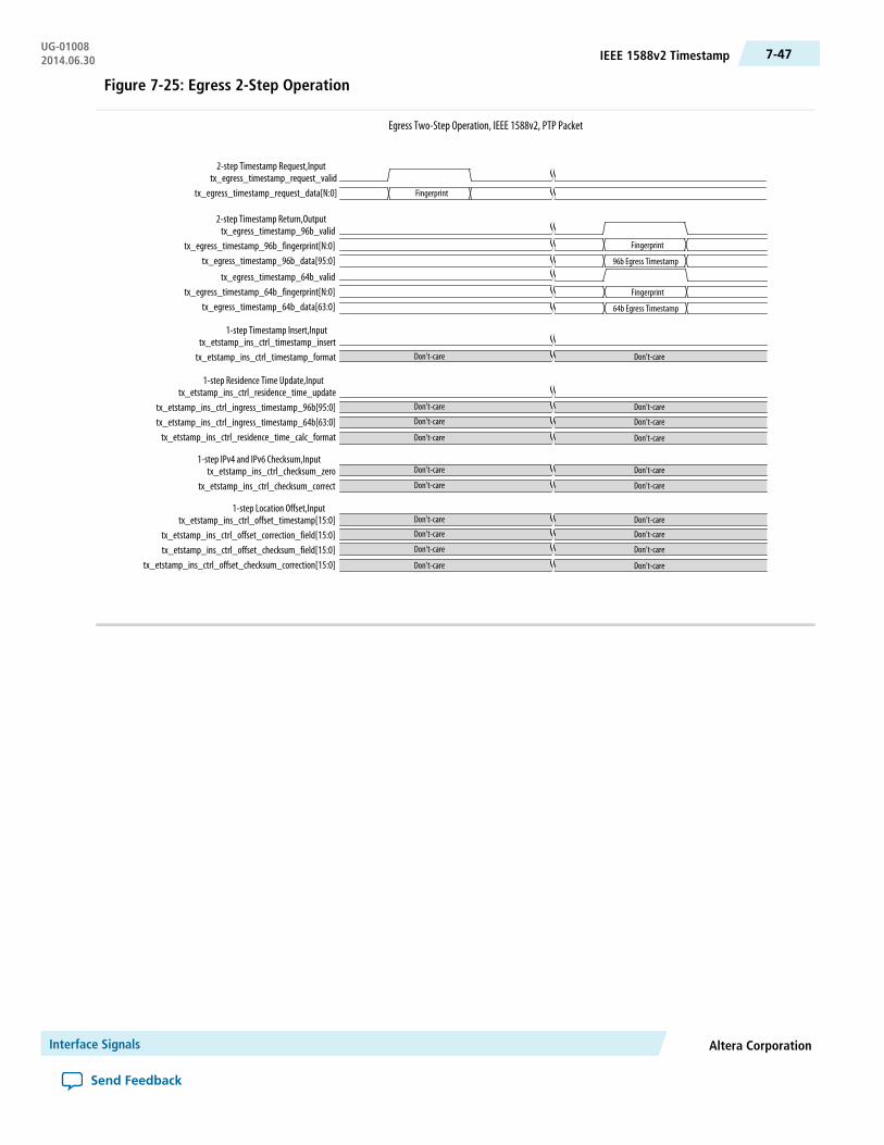
Figure 7-25: Egress 2-Step Operation
Egress Two-Step Operation, IEEE 1588v2, PTP Packet
2-step Timestamp Request,Inputtx_egress_timestamp_request_valid
tx_egress_timestamp_request_data[N:0]
2-step Timestamp Return,Outputtx_egress_timestamp_96b_valid
tx_egress_timestamp_96b_fingerprint[N:0]tx_egress_timestamp_96b_data[95:0]
tx_egress_timestamp_64b_validtx_egress_timestamp_64b_fingerprint[N:0]
tx_egress_timestamp_64b_data[63:0]
1-step Timestamp Insert,Inputtx_etstamp_ins_ctrl_timestamp_insert
tx_etstamp_ins_ctrl_timestamp_format
1-step Residence Time Update,Inputtx_etstamp_ins_ctrl_residence_time_update
tx_etstamp_ins_ctrl_ingress_timestamp_96b[95:0]tx_etstamp_ins_ctrl_ingress_timestamp_64b[63:0]tx_etstamp_ins_ctrl_residence_time_calc_format
1-step IPv4 and IPv6 Checksum,Inputtx_etstamp_ins_ctrl_checksum_zero
tx_etstamp_ins_ctrl_checksum_correct
1-step Location Offset,Inputtx_etstamp_ins_ctrl_offset_timestamp[15:0]
tx_etstamp_ins_ctrl_offset_correction_field[15:0]tx_etstamp_ins_ctrl_offset_checksum_field[15:0]
tx_etstamp_ins_ctrl_offset_checksum_correction[15:0]
Fingerprint
Fingerprint
96b Egress Timestamp
Fingerprint
64b Egress Timestamp
Don’t-care
Don’t-care
Don’t-care
Don’t-care
Don’t-care
Don’t-care
Don’t-care
Don’t-care
Don’t-care
Don’t-care
Don’t-care
Don’t-care
Don’t-care
Don’t-care
Don’t-care
Don’t-care
Don’t-care
Don’t-care
Don’t-care
Don’t-care
Altera CorporationInterface Signals
Send Feedback
7-47IEEE 1588v2 TimestampUG-010082014.06.30

8Design Considerations
2014.06.30
UG-01008 Subscribe Send Feedback
Optimizing Clock Resources in Multiport MAC with PCS and Embedded PMAThe following factors determine the total number of global and regional clock resources required by yoursystem:
• Configuration of the Triple-Speed Ethernet MegaCore function and the blocks it contains• PCS operating mode (SGMII or 1000BASE-X)• PMA technology implemented in the target device• Number of clocks that can share a single source• Number of PMAs required in the design• ALTGX megafunction operating mode
You can use the same clock source to drive clocks that are visible at the top-level design, thus reducing thetotal number of clock sources required by the entire design.
Table 8-1: Clock Signals Visible at Top-Level Design
Clock and reset signals that are visible at the top-level design for each possible configuration.Configurations(1)
ClocksMAC and PCS with PMAMAC and PCSMAC Only
Yes——rx_recovclkout
Yes——ref_clk
YesYesYesclk
YesYesYesff_tx_clk
YesYesYesff_rx_clk
NoNoYestx_clk
NoNoYesrx_clk
NoYes—tbi_rx_clk
NoYes—tbi_tx_clk
Yes——gxb_cal_blk_clk(2)
Yes——reconfig_clk
ISO9001:2008Registered
© 2014 Altera Corporation. All rights reserved. ALTERA, ARRIA, CYCLONE, ENPIRION, MAX, MEGACORE, NIOS, QUARTUS and STRATIX wordsand logos are trademarks of Altera Corporation and registered in the U.S. Patent and Trademark Office and in other countries. All otherwords and logos identified as trademarks or service marks are the property of their respective holders as described atwww.altera.com/common/legal.html. Altera warrants performance of its semiconductor products to current specifications in accordance withAltera's standard warranty, but reserves the right to make changes to any products and services at any time without notice. Altera assumesno responsibility or liability arising out of the application or use of any information, product, or service described herein except as expresslyagreed to in writing by Altera. Altera customers are advised to obtain the latest version of device specifications before relying on any publishedinformation and before placing orders for products or services.
www.altera.com
101 Innovation Drive, San Jose, CA 95134
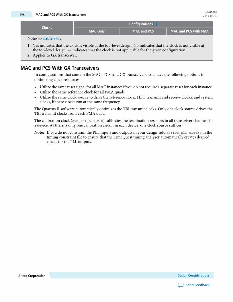
Configurations(1)Clocks
MAC and PCS with PMAMAC and PCSMAC Only
Notes to Table 8-1 :
1. Yes indicates that the clock is visible at the top-level design. No indicates that the clock is not visible atthe top-level design. — indicates that the clock is not applicable for the given configuration.
2. Applies to GX transceiver.
MAC and PCS With GX TransceiversIn configurations that contain the MAC, PCS, and GX transceivers, you have the following options inoptimizing clock resources:
• Utilize the same reset signal for all MAC instances if you do not require a separate reset for each instance.• Utilize the same reference clock for all PMA quads• Utilize the same clock source to drive the reference clock, FIFO transmit and receive clocks, and system
clocks, if these clocks run at the same frequency.
The Quartus II software automatically optimizes the TBI transmit clocks. Only one clock source drives theTBI transmit clocks from each PMA quad.
The calibration clock (gxb_cal_blk_clk) calibrates the termination resistors in all transceiver channels ina device. As there is only one calibration circuit in each device, one clock source suffices.
If you do not constrain the PLL inputs and outputs in your design, add derive_pll_clocks in thetiming constraint file to ensure that the TimeQuest timing analyzer automatically creates derivedclocks for the PLL outputs.
Note:
Design ConsiderationsAltera Corporation
Send Feedback
UG-01008MAC and PCS With GX Transceivers8-2 2014.06.30

Figure 8-1: Clock Distribution in MAC and SGMII PCS with GXB Configuration—Optimal Case
Figure shows the optimal clock distribution scheme you can achieve in configurations that contain the10/100/1000 Ethernet MAC, SGMII PCS, and GX transceivers.
tbi _ tx _clk 1
tbi _ rx _clk 1
tbi _ rx _clk 2
tbi _ rx _clk 3
tbi _ rx _clk 4
Port 4
clk 1
clk 2
clk 3
clk 4
PCS 1
rx _clk 1
tx _clk 1
PCS 2
rx _clk 2
tx _clk 2
PCS 3
rx _clk 3
tx _clk 3
PCS 4rx _clk 4
tx _clk 4
4-port MAC
Port 2
Port 3
ref _clk
rx _clk 1
tx _clk 1
rx _clk 2
tx _clk 2
rx _clk 3
tx _clk 3
rx _clk 4
tx _clk 4
ALTGX(GIGE Mode )
ALTGX(GIGE Mode )
ALTGX(GIGE Mode )
QuadTransceivers
ALTGX(GIGE Mode )
cal_blk_clk
ref _clk
TosubsequentQ
uads,ifany
tbi _ tx _clk 2
tbi _ tx _clk 3
tbi _ tx _clk 4
Port 1
tx _clk _en 1
rx _clk _en 1
tx _clk _en 2
rx _clk _en 2
tx _clk _en 3
rx _clk _en 3
tx _clk _en 1
rx _clk _en 1
Note to Figure 8-1 :
1. The PMA layer in devices with GX transceivers uses ALTGX megafunctions.
In addition to the aforementioned optimization options, the TBI transmit and receive clocks can be used todrive the MAC transmit and receive clocks, respectively.
Altera CorporationDesign Considerations
Send Feedback
8-3MAC and PCS With GX TransceiversUG-010082014.06.30

Figure 8-2: Clock Distribution in MAC and 1000BASE-X PCS with GXB Configuration—Optimal Case
Figure shows the optimal clock distribution scheme you can achieve in configurations that contain the10/100/1000 Ethernet MAC, 1000Base-X PCS, and GX transceivers.
ALTGX(GIGE Mode )
ALTGX(GIGE Mode )
ALTGX(GIGE Mode )
QuadTransceivers
ALTGX(GIGE Mode )
Port 2
4 -port MAC
cal_blk_clkref _clk
tbi _ rx _clk 1
tbi _ rx _clk 2
tbi _ rx _clk 3
tbi _ rx _clk 4
rx _clk 1
tx _clk 1
rx _clk 2
tx _clk 2
rx _clk 3
tx _clk 3
TosubsequentQ
uads,ifany
Port 4
Port 3
rx _clk 4
tx _clk 4
clk 1
clk 2
clk 3
clk 4
PCS 1
PCS 2
PCS 3
PCS 4
tbi _ tx _clk
Port 1
Note to Figure 8–2 :
1. The PMA layer in devices with GX transceivers uses ALTGX megafunctions.
MAC and PCS With LVDS Soft-CDR I/OIn configurations that contain the MAC, PCS, and LVDS Soft-CDR I/O, you have the following options inoptimizing clock resources:
• Utilize the same reset signal for all MAC instances if you do not require a separate reset for each instance.• Utilize the same clock source to drive the reference clock, FIFO transmit and receive clocks, and system
clocks, if these clocks run at the same frequency.
Design ConsiderationsAltera Corporation
Send Feedback
UG-01008MAC and PCS With LVDS Soft-CDR I/O8-4 2014.06.30
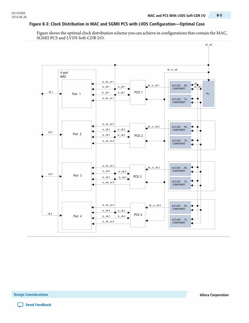
Figure 8-3: Clock Distribution in MAC and SGMII PCS with LVDS Configuration—Optimal Case
Figure shows the optimal clock distribution scheme you can achieve in configurations that contain theMAC,SGMII PCS and LVDS Soft-CDR I/O.
tbi _ tx _clk
tbi _ rx _clk 1
tbi _ rx _clk 2
tbi _ rx _clk 3
tbi _ rx _clk 4
clk 1
clk 2
clk 3
clk 4
PCS 1
rx _clk 1
tx _clk 1
PCS 2
rx _clk 2
tx _clk 2
PCS 3
rx _clk 3
tx _clk 3
PCS 4rx _clk 4
tx _clk 4
4-portMAC
Port 1
ref _clk
ALTLVDS _RX _COMPONENT
ALTLVDS _TX _COMPONENT
PLL
ALTLVDS _RX _COMPONENT
ALTLVDS _TX _COMPONENT
ALTLVDS _RX _COMPONENT
ALTLVDS _TX _COMPONENT
ALTLVDS _RX _COMPONENT
ALTLVDS _TX _COMPONENT
pllpll ~clk 1rx _clk 1
tx _clk 1
rx _clk 2
tx _clk 2
rx _clk 3
tx _clk 3
rx _clk 4
tx _clk 4
Port 2
Port 3
Port 4
tx _clk _en 1
rx _clk _en 1
tx _clk _en 2
rx _clk _en 2
tx _clk _en 3
rx _clk _en 3
tx _clk _en 4
rx _clk _en 4
Altera CorporationDesign Considerations
Send Feedback
8-5MAC and PCS With LVDS Soft-CDR I/OUG-010082014.06.30
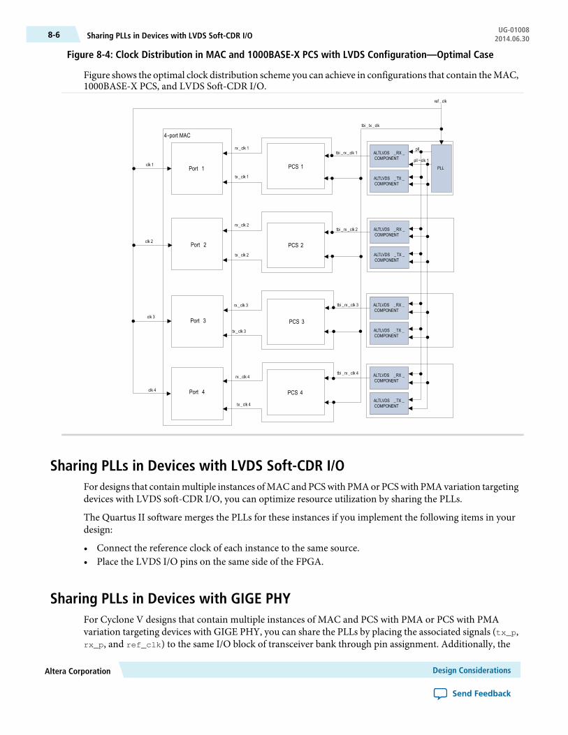
Figure 8-4: Clock Distribution in MAC and 1000BASE-X PCS with LVDS Configuration—Optimal Case
Figure shows the optimal clock distribution scheme you can achieve in configurations that contain theMAC,1000BASE-X PCS, and LVDS Soft-CDR I/O.
Port 1
4-port MACtbi _ tx _clk
tbi _rx _clk 1
tbi _rx _clk 2
tbi _rx _clk 3
tbi _rx _clk 4
rx _clk 1
tx _clk 1
rx _clk 2
tx _clk 2
rx _clk 3
tx _clk 3
Port 4
Port 3
rx _clk 4
tx _clk 4
clk 1
clk 2
clk 3
clk 4
PCS 1
PCS 2
PCS 3
PCS 4
ref _clk
ALTLVDS _RX _COMPONENT
ALTLVDS _TX _COMPONENT
PLL
ALTLVDS _RX _COMPONENT
ALTLVDS _TX _COMPONENT
ALTLVDS _RX _COMPONENT
ALTLVDS _TX _COMPONENT
ALTLVDS _RX _COMPONENT
ALTLVDS _TX _COMPONENT
pll
pll ~clk 1
Port 2
Sharing PLLs in Devices with LVDS Soft-CDR I/OFor designs that containmultiple instances ofMAC and PCSwith PMAor PCSwith PMAvariation targetingdevices with LVDS soft-CDR I/O, you can optimize resource utilization by sharing the PLLs.
The Quartus II software merges the PLLs for these instances if you implement the following items in yourdesign:
• Connect the reference clock of each instance to the same source.• Place the LVDS I/O pins on the same side of the FPGA.
Sharing PLLs in Devices with GIGE PHYFor Cyclone V designs that contain multiple instances of MAC and PCS with PMA or PCS with PMAvariation targeting devices with GIGE PHY, you can share the PLLs by placing the associated signals (tx_p,rx_p, and ref_clk) to the same I/O block of transceiver bank through pin assignment. Additionally, the
Design ConsiderationsAltera Corporation
Send Feedback
UG-01008Sharing PLLs in Devices with LVDS Soft-CDR I/O8-6 2014.06.30

rx_recovclkout clock must be buffered by two levels of inverter in the top level module so that it can befitted to the general I/O pins.
Sharing Transceiver QuadsFor designs that contain multiple PMA blocks targeting Altera device families with GX transceivers, youcan combine the transceiver channels in the same quad. To share the same transceiver quad, the transceiverchannels must have the same dynamic reconfiguration setting. In other words, you must turn on dynamicreconfiguration capabilities in all channels in a quad even though you only intend to use these capabilitiesin some of the channels.
The dynamic reconfiguration is always turned on in devices other than Arria GX and Stratix II GX. Whenthe dynamic reconfiguration is turned on in designs targeting devices other than StratixV,Altera recommendsthat you connect the dynamic reconfiguration signals to the ALTGX_RECONFIG megafunction.
In Stratix V devices, Altera recommends that you connect the dynamic reconfiguration signals to theTransceiver Reconfiguration Controller megafunction. For transceiver quad sharing between Triple-SpeedEthernet IP core and other IP cores that target Stratix V devices, reset signal for all the cores must be fromthe same source.
Refer to the respective device handbook for more information on dynamic reconfiguration signals in Alteradevices.
Migrating From Old to New User Interface For Existing DesignsIn Quartus II software ACDS 13.0 release, the old Triple-Speed Ethernet MegaCore function user interfaceis deprecated. Existing Triple-Speed Ethernet designs generated prior to the ACDS 13.0 release can still loadproperly in ACDS 13.0. However, starting from ACDS 13.1 release, the old Triple-Speed Ethernet interfaceand the design generated using the old interface will not be supported.
You need to manually migrate your design to the new user interface. Reopening and saving the existingdesign created with the old user interface will not automatically convert the design to the new user interface.
Tomigrate your design to the new user interface, launch theQuartus II softwareACDS 13.0 or higher, createa new project, and specify the parameters as described in Design Walkthrough on page 2-6.
Exposed Ports in the New User InterfaceIn the new user interface in Qsys, for a design that has a MAC function, you have to manually connect theexposed ports or terminate them.
In MAC variation with internal FIFO buffers, the ready latency is two in both standalone and Qsys flow.The Qsys system inserts a timing adapter to change the ready latency to zero.
Table 8-2: Exposed Ports and Recommended Termination Value for MAC Variation With Internal FIFO Buffers
Recommended Termination ValueWidthI/OPort Name
1'b01Ixon_gen
1'b01Ixoff_gen
Left open1Omagic_wakeup
Altera CorporationDesign Considerations
Send Feedback
8-7Sharing Transceiver QuadsUG-010082014.06.30
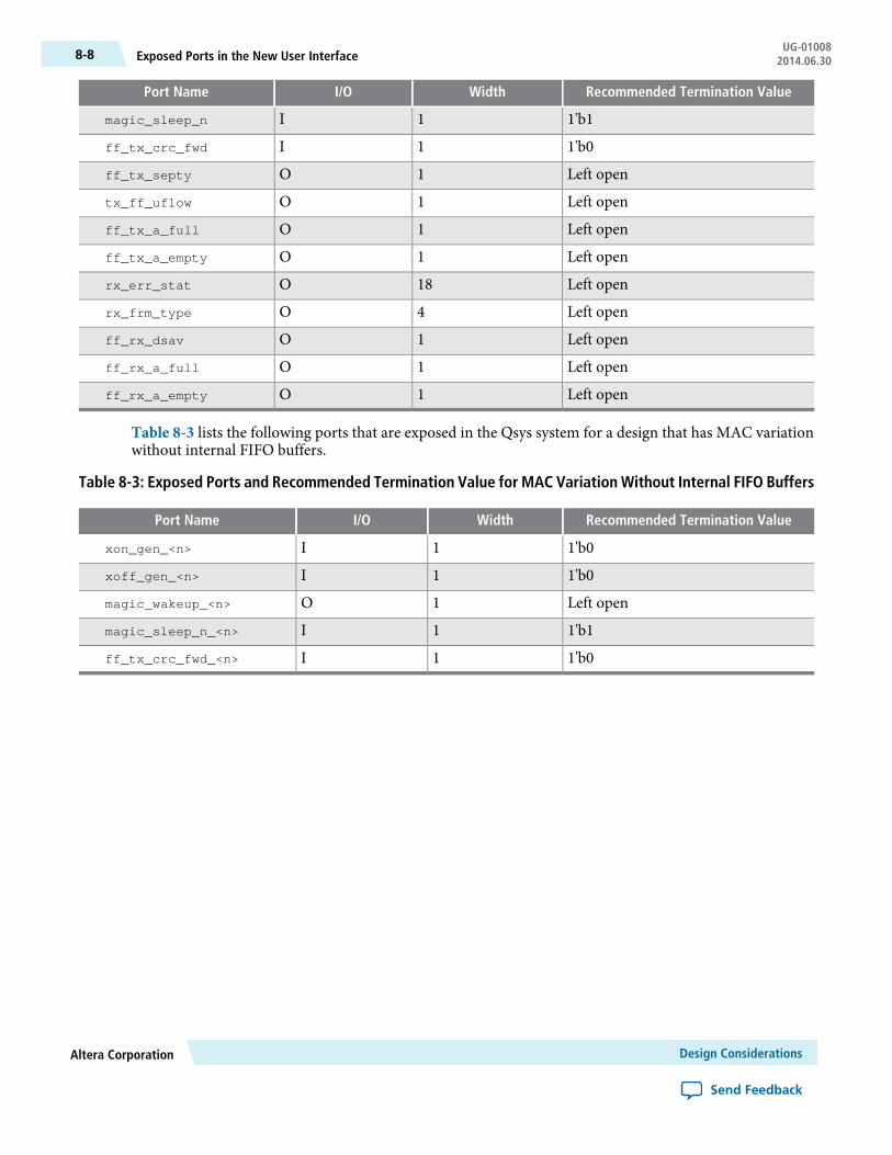
Recommended Termination ValueWidthI/OPort Name
1'b11Imagic_sleep_n
1'b01Iff_tx_crc_fwd
Left open1Off_tx_septy
Left open1Otx_ff_uflow
Left open1Off_tx_a_full
Left open1Off_tx_a_empty
Left open18Orx_err_stat
Left open4Orx_frm_type
Left open1Off_rx_dsav
Left open1Off_rx_a_full
Left open1Off_rx_a_empty
Table 8-3 lists the following ports that are exposed in the Qsys system for a design that has MAC variationwithout internal FIFO buffers.
Table 8-3: Exposed Ports and Recommended Termination Value for MAC Variation Without Internal FIFO Buffers
Recommended Termination ValueWidthI/OPort Name
1'b01Ixon_gen_<n>
1'b01Ixoff_gen_<n>
Left open1Omagic_wakeup_<n>
1'b11Imagic_sleep_n_<n>
1'b01Iff_tx_crc_fwd_<n>
Design ConsiderationsAltera Corporation
Send Feedback
UG-01008Exposed Ports in the New User Interface8-8 2014.06.30

9Timing Constraints
2014.06.30
UG-01008 Subscribe Send Feedback
Altera provides timing constraint files (.sdc) to ensure that the Triple-Speed Ethernet MegaCore functionmeets the design timing requirements in Altera devices. The files constraints the false paths and multi-cyclepaths in the Triple-Speed Ethernet Megacore function. The timing constraints files are specified in the<variation_name>.qip file and is automatically included in the Quartus II project files.
You may need to add timing constraints that are external to the MegaCore function. The following sectionsdescribe the procedure to create the timing constraint file.
Creating Clock ConstraintsAfter you generate and integrate the Triple-Speed Ethernet MegaCore function into the system, you needto create a timing constraints file to specify the clock constraint requirement.
You can specify the clock requirement in the timing constraint file using the following command:
create_clock
For example, for a new clock named "reg_clk", with a 50 MHz clock targeted to the top level input port"clk", enter the following command line:
create_clock -name "reg_clk" -period "50 MHz" [get_ports "clk"]
Figure 9–1 shows an example of how you can create a timing constraint file to constrain the Triple-SpeedEthernet MegaCore function clocks.
ISO9001:2008Registered
© 2014 Altera Corporation. All rights reserved. ALTERA, ARRIA, CYCLONE, ENPIRION, MAX, MEGACORE, NIOS, QUARTUS and STRATIX wordsand logos are trademarks of Altera Corporation and registered in the U.S. Patent and Trademark Office and in other countries. All otherwords and logos identified as trademarks or service marks are the property of their respective holders as described atwww.altera.com/common/legal.html. Altera warrants performance of its semiconductor products to current specifications in accordance withAltera's standard warranty, but reserves the right to make changes to any products and services at any time without notice. Altera assumesno responsibility or liability arising out of the application or use of any information, product, or service described herein except as expresslyagreed to in writing by Altera. Altera customers are advised to obtain the latest version of device specifications before relying on any publishedinformation and before placing orders for products or services.
www.altera.com
101 Innovation Drive, San Jose, CA 95134

Figure 9-1: Triple-Speed Ethernet Timing Constraint Example
user_instance.v
TOP.v
Altera PLL
10/100/1000-Mbps Ethernet MACwith 1000BASE-X/SGMII
PCS and PMA(with internal FIFO)ff_tx_clk
ff_rx_clk
tse_variation.v
ref_clk
clk
ext_clkpll_inclk100-Mhz 50-Mhz
110-Mhz
inclk0
c1 c0
xcvr_ref_clk125-Mhz
Note to Figure 9–2:
1. reconfig_clk is not shown in this example. Constrain reconfig_clk based on your design implemen-tation.
The example in above consists of the following Verilog modules:
• TOP.v—The top level design module which contains an Altera PLL and a user-defined instance. The toplevel input clocks consist of pll_inclk, ext_clk, and xcvr_ref_clk.
• user_instance.v—The user-defined instance that instantiates theTriple-SpeedEthernetMegaCore function.• tse_variation.v—ATriple-Speed EthernetMegaCore function variation. This example uses a 10/100/1000-
Mbps Ethernet MAC with an internal FIFO buffer, a 1000BASE-X/SGMII PCS, and an embedded PMA.
The frequency for the PLL clock input, inclk0, is 100 MHz, and the frequency for the PLL clock output, c0,is 110 MHz. The Triple-Speed Ethernet MAC Avalon-ST clocks, ff_tx_clk and ff_rx_clk, use c0 as theclock source. The input clock frequency for the transceiver reference clock, xcvr_ref_clk, is 125 MHz.
Example of the Triple-Speed Ethernet MegaCore function timing constraint file:
# PLL clock input, 100 MHzcreate_clock -name pll_inclk -period 10.000 [get_ports {pll_inclk}]
# ext_clk, 50 MHzcreate_clock -name ext_clk -period 20.000 [get_ports {pll_ext_clk}]
# xcvr_ref_clk, 125 MHzcreate_clock -name xcvr_ref_clk -period 8.000 [get_ports {xcvr_ref_clk}]
# Derive PLL generated output clocks.derive_pll_clocks
Timing ConstraintsAltera Corporation
Send Feedback
UG-01008Creating Clock Constraints9-2 2014.06.30
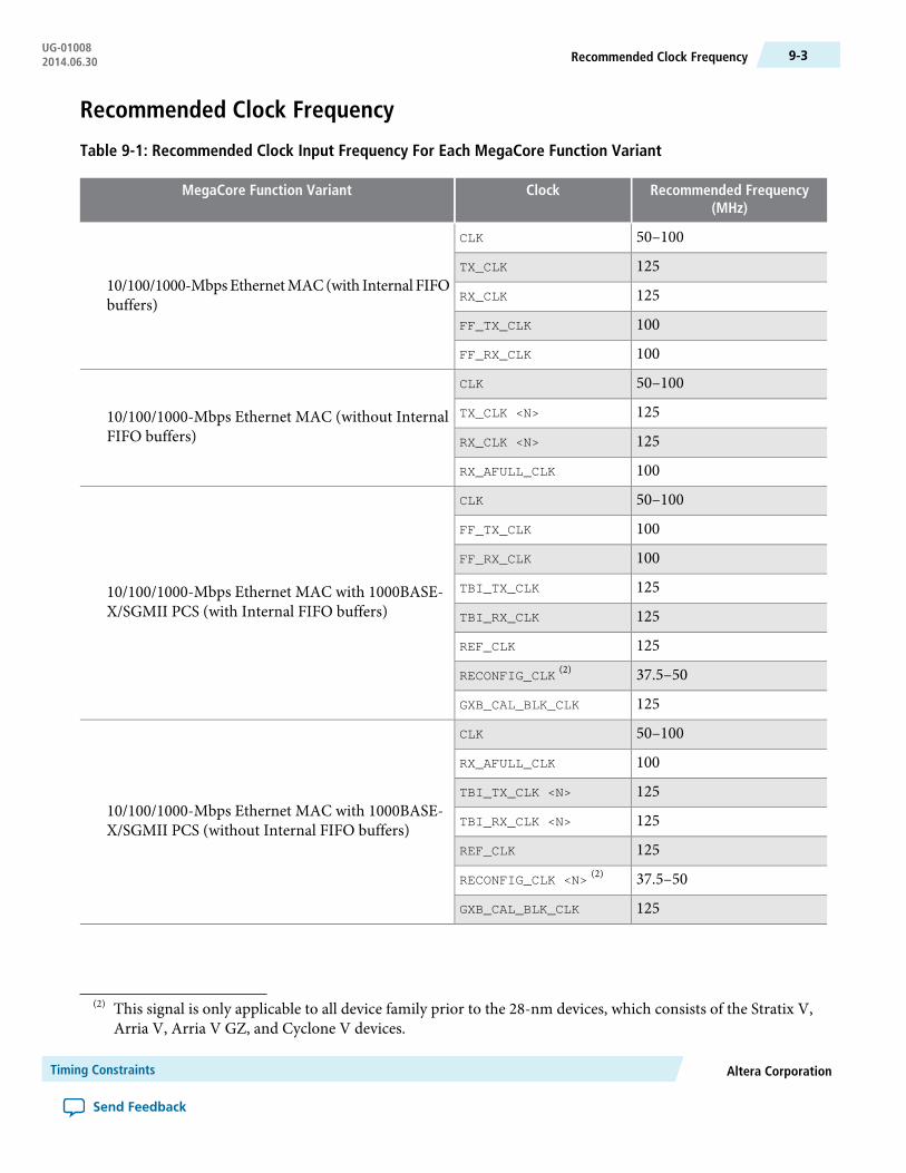
Recommended Clock Frequency
Table 9-1: Recommended Clock Input Frequency For Each MegaCore Function Variant
Recommended Frequency(MHz)
ClockMegaCore Function Variant
50–100CLK
10/100/1000-MbpsEthernetMAC(with Internal FIFObuffers)
125TX_CLK
125RX_CLK
100FF_TX_CLK
100FF_RX_CLK
50–100CLK
10/100/1000-Mbps Ethernet MAC (without InternalFIFO buffers)
125TX_CLK <N>
125RX_CLK <N>
100RX_AFULL_CLK
50–100CLK
10/100/1000-Mbps Ethernet MAC with 1000BASE-X/SGMII PCS (with Internal FIFO buffers)
100FF_TX_CLK
100FF_RX_CLK
125TBI_TX_CLK
125TBI_RX_CLK
125REF_CLK
37.5–50RECONFIG_CLK(2)
125GXB_CAL_BLK_CLK
50–100CLK
10/100/1000-Mbps Ethernet MAC with 1000BASE-X/SGMII PCS (without Internal FIFO buffers)
100RX_AFULL_CLK
125TBI_TX_CLK <N>
125TBI_RX_CLK <N>
125REF_CLK
37.5–50RECONFIG_CLK <N>(2)
125GXB_CAL_BLK_CLK
(2) This signal is only applicable to all device family prior to the 28-nm devices, which consists of the Stratix V,Arria V, Arria V GZ, and Cyclone V devices.
Altera CorporationTiming Constraints
Send Feedback
9-3Recommended Clock FrequencyUG-010082014.06.30

Recommended Frequency(MHz)
ClockMegaCore Function Variant
50–100CLK
1000BASE-X/SGMII PCS only125REF_CLK
125TBI_TX_CLK
125TBI_RX_CLK
Timing ConstraintsAltera Corporation
Send Feedback
UG-01008Recommended Clock Frequency9-4 2014.06.30
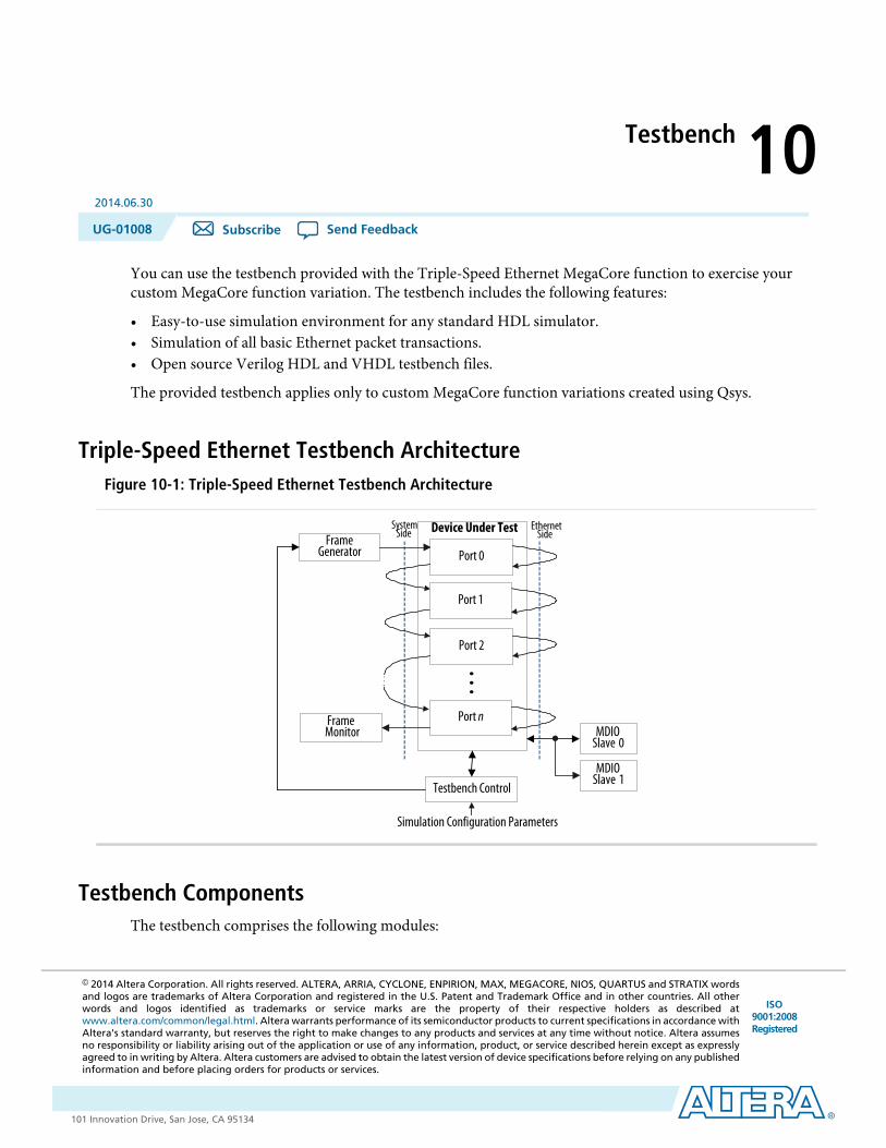
10Testbench
2014.06.30
UG-01008 Subscribe Send Feedback
You can use the testbench provided with the Triple-Speed Ethernet MegaCore function to exercise yourcustom MegaCore function variation. The testbench includes the following features:
• Easy-to-use simulation environment for any standard HDL simulator.• Simulation of all basic Ethernet packet transactions.• Open source Verilog HDL and VHDL testbench files.
The provided testbench applies only to custom MegaCore function variations created using Qsys.
Triple-Speed Ethernet Testbench ArchitectureFigure 10-1: Triple-Speed Ethernet Testbench Architecture
Device Under TestFrame
Generator
SystemSide
EthernetSide
Port 0
Port 2
Port n
...
Port 1
FrameMonitor MDIO
Slave 0
MDIOSlave 1
Testbench Control
Simulation Configuration Parameters
Testbench ComponentsThe testbench comprises the following modules:
ISO9001:2008Registered
© 2014 Altera Corporation. All rights reserved. ALTERA, ARRIA, CYCLONE, ENPIRION, MAX, MEGACORE, NIOS, QUARTUS and STRATIX wordsand logos are trademarks of Altera Corporation and registered in the U.S. Patent and Trademark Office and in other countries. All otherwords and logos identified as trademarks or service marks are the property of their respective holders as described atwww.altera.com/common/legal.html. Altera warrants performance of its semiconductor products to current specifications in accordance withAltera's standard warranty, but reserves the right to make changes to any products and services at any time without notice. Altera assumesno responsibility or liability arising out of the application or use of any information, product, or service described herein except as expresslyagreed to in writing by Altera. Altera customers are advised to obtain the latest version of device specifications before relying on any publishedinformation and before placing orders for products or services.
www.altera.com
101 Innovation Drive, San Jose, CA 95134
• Device under test (DUT)—Your custom MegaCore function variation• Avalon-ST Ethernet frame generator—Simulates a user application connected to the MAC system-side
interface. It generates frames on the Avalon-ST transmit interface.• Avalon-STEthernet framemonitor—Simulates a user application receiving frames from theMAC system-
side interface. It monitors the Avalon-ST receive interface and decodes all data received.• MII/RGMII/GMII Ethernet frame generator—Simulates a MAC function that sends frames to the PCS
function.• MII/RGMII/GMII Ethernet frame monitor—Simulates a MAC function that receives frames from the
PCS function and decodes them.• MDIO slaves—Simulates a PHY management interface. It responds to an MDIO master transactor.• Clock and reset generator.
Table 10-1: Testbench Components
Frame MonitorFrame GeneratorEthernet-SideInterface
System-SideInterface
Configuration
Avalon-ST FrameMonitor
Avalon-ST FrameGenerator
GMII/MII/RGMII
Avalon-STMAC only
Avalon-ST FrameMonitor
Avalon-ST FrameGenerator
TBIAvalon-STMAC with PCS
Avalon-ST FrameMonitor
Avalon-ST FrameGenerator
1.25 GbpsAvalon-STMAC with PCS andembedded PMA
GMII/MII FrameMonitor
GMII/MII FrameGenerator
TBIGMII/MIIPCS only
GMII/MII FrameMonitor
GMII/MII FrameGenerator
1.25 GbpsGMII/MIIPCS with embeddedPMA
Testbench VerificationThe testbench is self-checking and determines the success of a simulation by verifying the frames received.It also checks for any errors detected by the frame monitors. The testbench does not verify the IEEE statisticsgenerated by the MAC layer. Simulation fails only if the testbench is not able to detect deliberately insertederrors. At the end of a simulation, the testbench displays messages in the simulator console indicating itsresults.
The testbench verifies the following functionality:
• Transmit and receive datapaths are functionally correct.• Ethernet frames generated by the frame generator are received by the frame monitor.• Additional checks for configurations that contain the MAC function:
• Correct CRC-32 is inserted.• Short frames are padded up to at least 64 bytes in length.• Untagged received frames of size greater than themaximum frame length are truncated to themaximum
frame length with additional bytes up to 12.• CRC-32 is optionally discarded before the frames are received by the traffic monitor.
TestbenchAltera Corporation
Send Feedback
UG-01008Testbench Verification10-2 2014.06.30
• Additional checks for configurations that contain the PCS function with optional embedded PMA:
• Transmit frames generated by the frame generator are correctly encapsulated.• Received frames are de-encapsulated before they are forwarded to the frame monitor.
Testbench ConfigurationThe testbench is configured, by default, to operate in loopback mode. Frames sent through the transmit pathare looped back into the receive path.
Separate data paths can be configured for single-channel MAC with internal FIFO buffers. In this configu-ration, the MII/GMII Ethernet frame generator is enabled and the testbench control block simulatesindependent yet complete receive and transmit datapaths.
You can also customize other aspects of the testbench using the testbench simulation parameters.
The device under test is configured with the following default settings:
• Link speed is set to Gigabit except for configurations that contain Small MAC. For Small MACs, thedefault speed is 100 Mbps.
• Five Ethernet frames of payload length 100, 101, 102, 103 and 104 bytes are transmitted to the system-side interface and looped back on the ethernet-side interface.
• Default settings for the MAC function:
• The command_config register is set to 0x0408003B.• Promiscuous mode is enabled.• The maximum frame length, register frm_length, is configured to 1518.• For a single-channel MAC with internal FIFO buffers, the transmit FIFO buffer is set to start data
transmission as soon as its level reaches tx_section_full. The receive FIFO buffer is set to beginforwarding Ethernet frames to theAvalon-ST receive interfacewhen its level reaches rx_section_full.
• Default setting for the PCS function:
• The if_mode register is set to 0x0000.• Auto-negotiation between the local PHY and remote link PHY is bypassed.
Test FlowThe testbench performs the following operations upon a simulated power-on reset:
• Initializes the DUT registers.• Starts transmission. For a single-channel MAC with internal FIFO buffers, clears the FIFOs.• Ends transmission and checks the following elements to determine that the simulation is successful:
• No Ethernet protocol errors detected.• Ethernet frames generated and transmitted are received by the frame monitor.
Altera CorporationTestbench
Send Feedback
10-3Testbench ConfigurationUG-010082014.06.30

Simulation ModelThis section describes the step-by-step instructions for generating the simulation model and simulating yourdesign using the ModelSim simulator or other simulators.
Generate the Simulation ModelThe generated design example includes both Verilog HDL and VHDL testbench files for the device undertest (DUT)—your custom MegaCore function variation.
To generate a Verilog functional simulation model, use the command prompt and run the quartus_sh -tgenerate_sim_verilog.tcl file. Alternatively, perform the following steps:
1. Launch the Quartus II software and browse to the <variation name>_testbench directory.2. Open the generate_sim.qpf file from the project directory.3. On the Tools menu, select Tcl Scripts and select the generate_sim_verilog.tcl file.4. Click Run.
To generate a VHDL functional simulation model, you can use the command prompt and run the quartus_sh -t generate_sim_vhdl.tcl file. Alternatively, perform the following steps:
1. Launch the Quartus II software and browse to the <variation name>_testbench directory.2. Open the generate_sim.qpf file from the project directory.3. On the Tools menu, select Tcl Scripts and browse to the generate_sim_vhdl.tcl file.4. Click Run.
Simulate the IP CoreYou can simulate your IP core variation with the functional simulation model and the testbench or designexample generated with your IP core. The functional simulation model and testbench files are generated ina project subdirectory. This directory may also include scripts to compile and run the testbench.
For a complete list of models or libraries required to simulate your IP core, refer to the scripts provided withthe testbench in Simulation Model Files on page 10-5.
Before you begin
Generate the simulation model as shown inGenerate the SimulationModel on page 10-4 before simulatingthe testbench design.
To use the ModelSim®
simulation software to simulate the testbench design, follow these steps:
1. For Verilog testbench design:a. Browse to the following project directory:
<variation name>_testbench/testbench_verilog/<variation name>b. Run the following command to set up the required libraries, to compile the generated IP Functional
simulation model, and to exercise the simulation model with the provided testbench:
run_<variation_name>_tb.tcl
2. For VHDL testbench design:a. Browse to the following project directory:
<variation name>_testbench/testbench_vhdl/<variation name>
TestbenchAltera Corporation
Send Feedback
UG-01008Simulation Model10-4 2014.06.30
b. Run the following command to set up the required libraries, to compile the generated IP Functionalsimulation model, and to exercise the simulation model with the provided testbench:
run_<variation_name>_tb.tcl
For more information about simulating Altera IP cores, refer to Simulating Altera Designs in volume3 of the Quartus II Handbook.
Use the simulation models only for simulation and not for synthesis or any other purposes. Usingthese models for synthesis creates a nonfunctional design.
Note:
Simulation Model FilesPreviously, the Triple-Speed Ethernet MegaCore function generates a <variation_name>.vho or<variation_name>.vo file for VHDL or Verilog HDL IP functional simulation model.
For the new Triple-Speed Ethernet MegaCore function created in Quartus II ACDS 13.0, the simulationmodel will be generated using the industrial standard IEEE simulation encryption.
Table 10-2 lists the scripts available for you to compile the simulation model files in a standalone flow.
Table 10-2: Simulation Model Files
DescriptionDirectory Name
Contains a ModelSim script msim_setup.tcl to set up and run asimulation.
<variation_name>_sim/mentor/
Contains a shell script vcs_setup.sh to set up and run aVCS®simulation.<variation_name>_sim/synopsys/
vcs
Contains a shell script vcsmx_setup.sh and synopsys_sim.setup to setup and run a VCS MX simulation.
<variation_name>_sim/synopsys/vcsmx
Contains a shell script ncsim_setup.sh and other setup files to set upand run an NCSIM simulation.
<variation_name>_sim/mentor/cadence
Altera CorporationTestbench
Send Feedback
10-5Simulation Model FilesUG-010082014.06.30

11Software Programming Interface
2014.06.30
UG-01008 Subscribe Send Feedback
Driver ArchitectureFigure 11-1: Triple-Speed Ethernet Software Driver Architecture
TX SGDMA
RX SGDMA
Memory
ClientApps
InternicheStack TSE Driver
Control Interface
TX FIFO (2)
RX FIFO (2)
TX Descriptor
RX Descriptor
TSE MAC
Descriptor Memory (1)
Nios II CPU
TX Path
RX Path
Avalon -MM Interface
SetupDescriptors
MII/GMII
MII/GMII
Proc
ess&
Writ
eBac
kSta
tus
Proc
ess&
Writ
eBac
kSta
tus
Notes to Figure 11–1 :
1. The first n bytes are reserved for SGDMA descriptors, where n = (Total number of descriptors + 3) × 32.Applications must not use this memory region.
2. For MAC variations without internal FIFO buffers, the transmit and receive FIFOs are external to theMAC function.
ISO9001:2008Registered
© 2014 Altera Corporation. All rights reserved. ALTERA, ARRIA, CYCLONE, ENPIRION, MAX, MEGACORE, NIOS, QUARTUS and STRATIX wordsand logos are trademarks of Altera Corporation and registered in the U.S. Patent and Trademark Office and in other countries. All otherwords and logos identified as trademarks or service marks are the property of their respective holders as described atwww.altera.com/common/legal.html. Altera warrants performance of its semiconductor products to current specifications in accordance withAltera's standard warranty, but reserves the right to make changes to any products and services at any time without notice. Altera assumesno responsibility or liability arising out of the application or use of any information, product, or service described herein except as expresslyagreed to in writing by Altera. Altera customers are advised to obtain the latest version of device specifications before relying on any publishedinformation and before placing orders for products or services.
www.altera.com
101 Innovation Drive, San Jose, CA 95134
Directory StructureStructure of the altera_triple_speed_ethernet directory.
Figure 11-2: Directory Structure
HAL
altera_triple_speed_ethernet
inctriple_speed_ethernet.haltera_avalon_tse.haltera_avalon_tse_system_info.h
inctriple_speed_ethernet_regs.h
srcaltera_avalon_tse.caltera_avalon_tse_system_info.c
inicheins_tse_mac.htriple_speed_ethernet_iniche.h
iniche
UCOSII
inc
src
ins_tse_mac.c
PHY DefinitionBy default, the software driver only supports the following PHYs:
• National DP83848C (10/100 Mbps)• National DP83865 (10/100/1000 Mbps)• Marvell 88E1111 (10/100/1000 Mbps)• Marvell 88E1145 (Quad PHY, 10/100/1000 Mbps).
You can extend the software driver to support other PHYs by defining the PHY profile using the structurealt_tse_phy_profile and adding it to the system using the function alt_tse_phy_add_profile(). Foreach PHY instance, use the structure alt_tse_system_phy_struct to define it and the functionalt_tse_system_add_sys() to add the instance to the system.
The software driver automatically detects the PHY’s operating mode and speed if the PHY conforms to thefollowing specifications:
• One bit to specify duplex and two consecutive bits (the higher bit being themost significant bit) to specifythe speed in the same extended PHY specific register.
• The speed bits are set according to the convention shown in Table 11-1.
Table 11-1: PHY Speed Bit Values
PHY Speed BitsSpeed (Mbps)
LSBMSB
011000
10100
Software Programming InterfaceAltera Corporation
Send Feedback
UG-01008Directory Structure11-2 2014.06.30
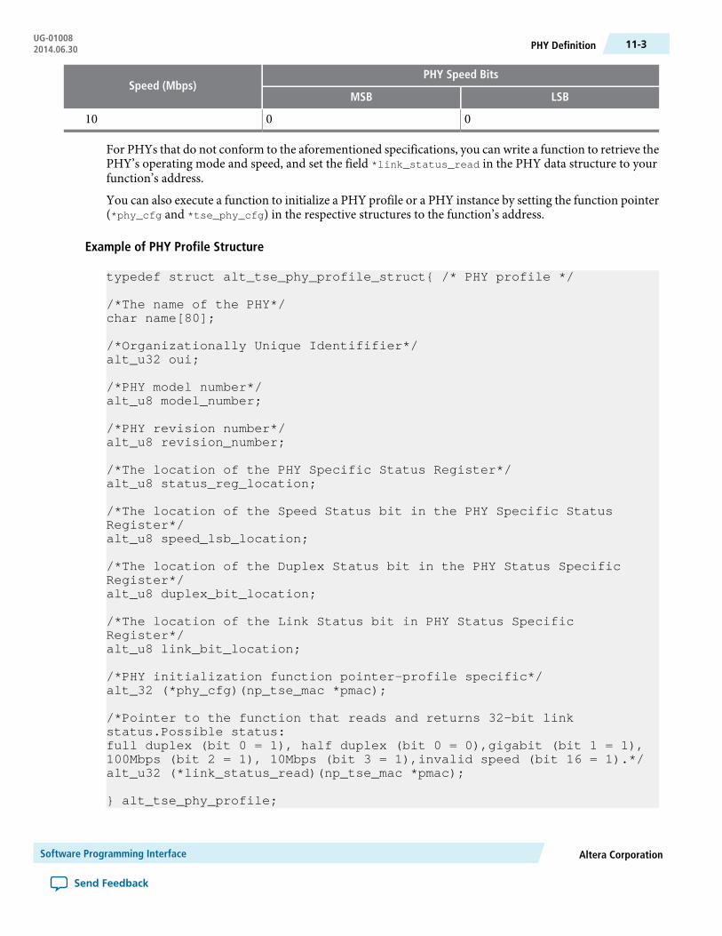
PHY Speed BitsSpeed (Mbps)
LSBMSB
0010
For PHYs that do not conform to the aforementioned specifications, you can write a function to retrieve thePHY’s operating mode and speed, and set the field *link_status_read in the PHY data structure to yourfunction’s address.
You can also execute a function to initialize a PHY profile or a PHY instance by setting the function pointer(*phy_cfg and *tse_phy_cfg) in the respective structures to the function’s address.
Example of PHY Profile Structure
typedef struct alt_tse_phy_profile_struct{ /* PHY profile */
/*The name of the PHY*/char name[80];
/*Organizationally Unique Identififier*/alt_u32 oui;
/*PHY model number*/alt_u8 model_number;
/*PHY revision number*/alt_u8 revision_number;
/*The location of the PHY Specific Status Register*/alt_u8 status_reg_location;
/*The location of the Speed Status bit in the PHY Specific StatusRegister*/alt_u8 speed_lsb_location;
/*The location of the Duplex Status bit in the PHY Status SpecificRegister*/alt_u8 duplex_bit_location;
/*The location of the Link Status bit in PHY Status SpecificRegister*/alt_u8 link_bit_location;
/*PHY initialization function pointer—profile specific*/alt_32 (*phy_cfg)(np_tse_mac *pmac);
/*Pointer to the function that reads and returns 32-bit link status.Possible status:full duplex (bit 0 = 1), half duplex (bit 0 = 0),gigabit (bit 1 = 1),100Mbps (bit 2 = 1), 10Mbps (bit 3 = 1),invalid speed (bit 16 = 1).*/alt_u32 (*link_status_read)(np_tse_mac *pmac);
} alt_tse_phy_profile;
Altera CorporationSoftware Programming Interface
Send Feedback
11-3PHY DefinitionUG-010082014.06.30

Example of PHY Instance Structure
typedef struct alt_tse_system_phy_struct { /* PHY instance */
/* PHY's MDIO address */alt_32tse_phy_mdio_address;/* PHY initialization function pointer—instance specific */alt_32 (*tse_phy_cfg)(np_tse_mac *pmac);
} alt_tse_system_phy;
Using Multiple SG-DMA DescriptorsTo successfully use multiple SG-DMA descriptors in your application, make the following modifications:
• Set the value of the constant ALTERA_TSE_SGDMA_RX_DESC_CHAIN_SIZE in altera_avalon_tse.h to thenumber of descriptors optimal for your application. The default value is 1 and the maximum value isdetermined by the constant NUMBIGBUFFS. For TCP applications, Altera recommends that you use thedefault value.
• Increase the amount of memory allocated for the Interniche stack.
Thememory space for the Interniche stack is allocated using the Interniche function pk_alloc(). Althoughuser applications and other network interfaces such as LAN91C111 can share the memory space, Alterarecommends that you use this memory space for only one purpose, that is storing unprocessed packetsfor the Triple-Speed Ethernet MegaCore function. Each SG-DMA descriptor used by the device driverconsumes a buffer size of 1536 bytes (defined by the constant BIGBUFSIZE) in the memory space. Toachieve reasonable performance and to avoidmemory exhaustion, add a new constant named NUMBIGBUFSto your application and set its value using the following guideline:
NUMBIGBUFS = <current value> + <number of SG-DMA descriptors>
By default, the constant NUMBIGBUFS is set to 30 in ipport.h. If you changed the default value in the previousrelease of the MegaCore function to optimize performance and resource usage, use the modified valueto compute the new value of NUMBIGBUFS.
Using Jumbo FramesTo use jumbo frames, set the frm_length register to 9600 and edit the files and definitions.
Table 11-2: Jumbo Frames Definitions
DefinitionFile
#define ALTERA_TSE_PKT_INIT_LEN 8206
#define ALTERA_TSE_MAX_MTU_SIZE 8192
#define ALTERA_TSE_MIN_MTU_SIZE 14
ip\altera\ethernet\altera_eth_tse\src\software\lib\UCOSII\inc\iniche\altera_eth_tse_iniche.h
#define ALTERA_TSE_MAC_MAX_FRAME_LENGTH 8196(1)ip\altera\ethernet\altera_eth_tse\src\software\lib\HAL\inc\altera_avalon_tse.h
Software Programming InterfaceAltera Corporation
Send Feedback
UG-01008Using Multiple SG-DMA Descriptors11-4 2014.06.30

DefinitionFile
#ifndef BIGBUFSIZE
#define BIGBUFSIZE 1536
#endif
<BSP project directory> \iniche\src\h\nios2\ipport.h
Note to Table 11-2 :
1. The maximum value for ALTERA_TSE_MAC_MAX_FRAME_LENGTH is defined by the frm_length register.
API FunctionsThis section describes each provided API function in alphabetical order.
alt_tse_mac_get_common_speed()Details
alt_tse_mac_get_common_speed(np_tse_mac *pmac)Prototype:
NoThread-safe:
NoAvailable from ISR:
<altera_avalon_tse.h>Include:
The alt_tse_mac_get_common_speed()obtains the common speed supported bythe PHYs connected to a multiport MAC and remote link partners.
Description:
pmac—A pointer to the base of the MAC control interface.Parameter:
TSE_PHY_SPEED_1000 if the PHYs common speed is 1000 Mbps. TSE_PHY_SPEED_100 if the PHYs common speed is 100 Mbps. TSE_PHY_SPEED_10 if the PHYscommon speed is 10 Mbps. TSE_PHY_SPEED_NO_COMMON if there isn’t a commonspeed among the PHYs.
Return:
alt_32 alt_tse_mac_set_common_speed()See also:
alt_tse_mac_set_common_speed()Details
alt_tse_mac_set_common_speed(np_tse_mac *pmac, alt_32 common_speed)Prototype:
NoThread-safe:
NoAvailable from ISR:
<altera_avalon_tse.h>Include:
The alt_tse_mac_set_common_speed() sets the speed of a multiport MAC andthe PHYs connected to it.
Description:
pmac—A pointer to the base of the MAC control interface.
common_speed—The speed to set.
Parameter:
Altera CorporationSoftware Programming Interface
Send Feedback
11-5API FunctionsUG-010082014.06.30

Details
TSE_PHY_SPEED_1000 if the PHYs common speed is 1000 Mbps.
TSE_PHY_SPEED_100 if the PHYs common speed is 100 Mbps.
TSE_PHY_SPEED_10 if the PHYs common speed is 10 Mbps.
TSE_PHY_SPEED_NO_COMMON if there isn’t a common speed among the PHYs. Thecurrent speed of the MAC and PHYs is not changed.
Return:
alt_32 alt_tse_mac_get_common_speed()See also:
alt_tse_phy_add_profile()Details
alt_tse_phy_add_profile(alt_tse_phy_profile *phy)Prototype:
NoThread-safe:
NoAvailable from ISR:
<altera_avalon_tse.h>Include:
The alt_tse_phy_add_profile() function adds a new PHY to the PHY profile.Use this function if you want to use PHYs other than Marvell 88E1111, MarvellQuad PHY 88E1145, National DP83865, and National DP83848C.
Description:
phy—A pointer to the PHY structure.Parameter:
ALTERA_TSE_MALLOC_FAILED if the operation is not successful. Otherwise, theindex of the newly added PHY is returned.
Return:
alt_tse_system_add_sys()
Details
alt_tse_system_add_sys(alt_tse_system_mac *psys_mac, alt_tse_system_
sgdma *psys_sgdma, alt_tse_system_desc_mem *psys_mem, alt_tse_system_
shared_fifo *psys_shared_fifo, alt_tse_system_phy *psys_phy)
Prototype:
NoThread-safe:
NoAvailable from ISR:
<system.h><system.h><altera_avalon_tse_system_info.h> <altera_avalon_tse.h><altera_avalon_tse_system_info.h><altera_avalon_tse_system_info.h><altera_avalon_tse_system_info.h>
Include:
The alt_tse_system_add_sys() function defines the TSE system’s components:MAC, scatter-gather DMA, memory, FIFO and PHY. This needs to be done foreach port in the system.
Description:
Software Programming InterfaceAltera Corporation
Send Feedback
UG-01008alt_tse_phy_add_profile()11-6 2014.06.30
Details
psys_mac—A pointer to the MAC structure.
psys_sgdma—A pointer to the scatter-gather DMA structure.
psys_mem—A pointer to the memory structure.
psys_shared_fifo—A pointer to the FIFO structure.
psys_phy—A pointer to the PHY structure.
Parameter:
SUCCESS if the operation is successful.SUCCESS if the operation is successful. ALTERA_TSE_MALLOC_FAILED if the operation fails. ALTERA_TSE_SYSTEM_DEF_ERROR if oneor more of the definitions are incorrect, or empty.
Return:
triple_speed_ethernet_init()Details
error_t triple_speed_ethernet_init(alt_niche_dev *p_dev)Prototype:
NoThread-safe:
NoAvailable from ISR:
<triple_speed_ethernet_iniche.h>Include:
The triple_speed ethernet_init() function opens and initializes the Triple-Speed Ethernet driver. Initialization involves the following operations:
• Set up the NET structure of the MAC device instance.• Configure the MAC PHY Address.• Register and open the SGDMARXandTXModule of theMACdevice instance.• Enable the SGDMA RX interrupt and register it to the Operating System.• Register the SGDMA RX callback function.• Obtains the PHY Speed of the MAC.• Set up the Ethernet MAC Register settings for the Triple-Speed Ethernet driver
operation.• Set up the initial descriptor chain to start the SGDMA RX operation.
Description:
p_dev—A pointer to the Triple-Speed Ethernet device instance.Parameter:
SUCCESS if the Triple-Speed Ethernet driver is successfully initialized.Return:
tse_mac_close()See also:
tse_mac_close()Details
int tse_mac_close(int iface)Prototype:
NoThread-safe:
NoAvailable from ISR:
Altera CorporationSoftware Programming Interface
Send Feedback
11-7triple_speed_ethernet_init()UG-010082014.06.30

Details
<triple_speed_ethernet_iniche.h>Include:
The tse_mac_close() closes the Triple-Speed Ethernet driver by performing thefollowing operations:
• Configure the admin and operation status of the NET structure of the Triple-Speed Ethernet driver instance to ALTERA_TSE_ADMIN_STATUS_DOWN.
• De-register the SGDMA RX interrupt from the operating system.• Clear the RX_ENA bit in the command_config register to disable the RX
datapath.
Description:
iface—The index of the MAC interface. This argument is reserved for configura-tions that contain multiple MAC instances.
Parameter:
SUCCESS if the close operations are successful. An error code if de-registration ofSGDMA RX from the operating system failed.
Return:
triple_speed_ethernet_init()See also:
tse_mac_raw_send()Details
int tse_mac_raw_send(NET net, char *data, unsigned data_bytes)Prototype:
NoThread-safe:
NoAvailable from ISR:
<triple_speed_ethernet_iniche.h>Include:
The tse_mac_raw_send() function sends Ethernet frames data to the MACfunction. It validates the arguments to ensure the data length is greater than theethernet header size specified by ALTERA_TSE_MIN_MTU_SIZE. The function alsoensures the SGDMA TX engine is not busy prior to constructing the descriptorfor the current transmit operation.
Upon successful validations, this function calls the internal API, tse_mac_sTxWrite, to initiate the synchronous SGDMA transmit operation on the currentdata buffer.
Description:
net—The NET structure of the Triple-Speed Ethernet MAC instance. data—Adata pointer to the base of the Ethernet frame data, including the header, to betransmitted to the MAC. The data pointer is assumed to be word-aligned. data_bytes—The total number of bytes in the Ethernet frame including the additionalpadding bytes as specified by ETHHDR_BIAS.
Parameter:
SUCCESS if the current data buffer is successfully transmitted.
SEND_DROPPED if the number of data bytes is less than the Ethernet header size.
ENP_RESOURCE if the SGDMA TX engine is busy.
Return:
Software Programming InterfaceAltera Corporation
Send Feedback
UG-01008tse_mac_raw_send()11-8 2014.06.30

tse_mac_setGMII mode()Details
int tse_mac_setGMIImode(np_tse_mac *pmac)Prototype:
NoThread-safe:
NoAvailable from ISR:
<triple_speed_ethernet_iniche.h>Include:
The tse_mac_setGMIImode() function sets the MAC function operation mode toGigabit (GMII). The settings of the command_config register are restored at theend of the function.
Description:
pmac—A pointer to the MAC control interface base address.Parameter:
SUCCESSReturn:
tse_mac_setMIImode()See also:
tse_mac_setMIImode()Details
int tse_mac_setMIImode(np_tse_mac *pmac)Prototype:
NoThread-safe:
NoAvailable from ISR:
<triple_speed_ethernet_iniche.h>Include:
The tse_mac_setMIImode() function sets the MAC function operation mode toMII (10/100). The settings of the command_config register are restored at the endof the function.
Description:
pmac—A pointer to the MAC control interface base address.Parameter:
SUCCESSReturn:
tse_mac_setGMIImode()See also:
tse_mac_SwReset()Details
int tse_mac_SwReset(np_tse_mac *pmac)Prototype:
NoThread-safe:
NoAvailable from ISR:
<triple_speed_ethernet_iniche.h>Include:
The tse_mac_SwReset() performs a software reset on the MAC function. Asoftware reset occurs with some latency as specified by ALTERA_TSE_SW_RESET_TIME_OUT_CNT. The settings of the command_config register are restored at theend of the function.
Description:
Altera CorporationSoftware Programming Interface
Send Feedback
11-9tse_mac_setGMII mode()UG-010082014.06.30

Details
pmac—A pointer to the MAC control interface base address.Parameter:
SUCCESSReturn:
ConstantsTable 11-3 lists all constants defined for the MAC registers manipulation and provides links to detaileddescriptions of the registers. It also list the constants that define the MAC operating mode and timeoutvalues.
Table 11-3: Constants Mapping
DescriptionValueConstant
0: Half-duplex 1: Full-duplex1ALTERA_TSE_DUPLEX_MODE_DEFAULT
0: 10 Mbps 1: 100 Mbps 2: 1000Mbps
0ALTERA_TSE_MAC_SPEED_DEFAULT
The number of SG-DMA descrip-tors required for the currentoperating mode.
1ALTERA_TSE_SGDMA_RX_DESC_CHAIN_SIZE
The timeout value when the MACtries to establish a link with a PHY.
1000000ALTERA_CHECKLINK_TIMEOUT_THRESHOLD
The auto-negotiation timeoutvalue.
250000ALTERA_AUTONEG_TIMEOUT_THRESHOLD
Command_Config Register (Command_Config Register (Dword Offset 0x02) on page 6-7)
Configures the TX_ENA bit.0ALTERA_TSEMAC_CMD_TX_ENA_OFST
0x1ALTERA_TSEMAC_CMD_TX_ENA_MSK
Configures the RX_ENA bit.1ALTERA_TSEMAC_CMD_RX_ENA_OFST
0x2ALTERA_TSEMAC_CMD_RX_ENA_MSK
Configures the XON_GEN bit.2ALTERA_TSEMAC_CMD_XON_GEN_OFST
0x4ALTERA_TSEMAC_CMD_XON_GEN_MSK
Configures the ETH_SPEED bit.3ALTERA_TSEMAC_CMD_ETH_SPEED_OFST
0x8ALTERA_TSEMAC_CMD_ETH_SPEED_MSK
Configures the PROMIS_EN bit.4ALTERA_TSEMAC_CMD_PROMIS_EN_OFST
0x10ALTERA_TSEMAC_CMD_PROMIS_EN_MSK
Configures the PAD_EN bit.5ALTERA_TSEMAC_CMD_PAD_EN_OFST
0x20ALTERA_TSEMAC_CMD_PAD_EN_MSK
Configures the CRC_FWD bit.6ALTERA_TSEMAC_CMD_CRC_FWD_OFST
0x40ALTERA_TSEMAC_CMD_CRC_FWD_MSK
Software Programming InterfaceAltera Corporation
Send Feedback
UG-01008Constants11-10 2014.06.30

DescriptionValueConstant
Configures the PAUSE_FWD bit.7ALTERA_TSEMAC_CMD_PAUSE_FWD_OFST
0x80ALTERA_TSEMAC_CMD_PAUSE_FWD_MSK
Configures the PAUSE_IGNORE bit.8ALTERA_TSEMAC_CMD_PAUSE_IGNORE_OFST
0x100ALTERA_TSEMAC_CMD_PAUSE_IGNORE_MSK
Configures the TX_ADDR_INS bit.9ALTERA_TSEMAC_CMD_TX_ADDR_INS_OFST
0x200ALTERA_TSEMAC_CMD_TX_ADDR_INS_MSK
Configures the HD_ENA bit.10ALTERA_TSEMAC_CMD_HD_ENA_OFST
0x400ALTERA_TSEMAC_CMD_HD_ENA_MSK
Configures the EXCESS_COL bit.11ALTERA_TSEMAC_CMD_EXCESS_COL_OFST
0x800ALTERA_TSEMAC_CMD_EXCESS_COL_MSK
Configures the LATE_COL bit.12ALTERA_TSEMAC_CMD_LATE_COL_OFST
0x1000ALTERA_TSEMAC_CMD_LATE_COL_MSK
Configures the SW_RESET bit.13ALTERA_TSEMAC_CMD_SW_RESET_OFST
0x2000ALTERA_TSEMAC_CMD_SW_RESET_MSK
Configures the MHASH_SEL bit.14ALTERA_TSEMAC_CMD_MHASH_SEL_OFST
0x4000ALTERA_TSEMAC_CMD_MHASH_SEL_MSK
Configures the LOOP_ENA bit.15ALTERA_TSEMAC_CMD_LOOPBACK_OFST
0x8000ALTERA_TSEMAC_CMD_LOOPBACK_MSK
Configures the TX_ADDR_SEL bits(bits 16 - 18).
16ALTERA_TSEMAC_CMD_TX_ADDR_SEL_OFST
0x70000ALTERA_TSEMAC_CMD_TX_ADDR_SEL_MSK
Configures the MAGIC_ENA bit.19ALTERA_TSEMAC_CMD_MAGIC_ENA_OFST
0x80000ALTERA_TSEMAC_CMD_MAGIC_ENA_MSK
Configures the SLEEP bit.20ALTERA_TSEMAC_CMD_SLEEP_OFST
0x100000ALTERA_TSEMAC_CMD_SLEEP_MSK
Configures the WAKEUP bit.21ALTERA_TSEMAC_CMD_WAKEUP_OFST
0x200000ALTERA_TSEMAC_CMD_WAKEUP_MSK
Configures the XOFF_GEN bit.22ALTERA_TSEMAC_CMD_XOFF_GEN_OFST
0x400000ALTERA_TSEMAC_CMD_XOFF_GEN_MSK
Configures the CNTL_FRM_ENA bit.23ALTERA_TSEMAC_CMD_CNTL_FRM_ENA_OFST
0x800000ALTERA_TSEMAC_CMD_CNTL_FRM_ENA_MSK
Configures the NO_LENGTH_CHECKbit.
24ALTERA_TSEMAC_CMD_NO_LENGTH_CHECK_OFST
0x1000000ALTERA_TSEMAC_CMD_NO_LENGTH_CHECK_MSK
Altera CorporationSoftware Programming Interface
Send Feedback
11-11ConstantsUG-010082014.06.30

DescriptionValueConstant
Configures the ENA_10 bit.25ALTERA_TSEMAC_CMD_ENA_10_OFST
0x2000000ALTERA_TSEMAC_CMD_ENA_10_MSK
Configures the RX_ERR_DISC bit.26ALTERA_TSEMAC_CMD_RX_ERR_DISC_OFST
0x4000000ALTERA_TSEMAC_CMD_RX_ERR_DISC_MSK
Configures the CNT_RESET bit.31ALTERA_TSEMAC_CMD_CNT_RESET_OFST
0x80000000ALTERA_TSEMAC_CMD_CNT_RESET_MSK
Tx_Cmd_StatRegister (Transmit andReceiveCommandRegisters (DwordOffset 0x3A– 0x3B) on page6-13)
Configures the OMIT_CRC bit.17ALTERA_TSEMAC_TX_CMD_STAT_OMITCRC_OFST
0x20000ALTERA_TSEMAC_TX_CMD_STAT_OMITCRC_MSK
Configures the TX_SHIFT16 bit.18ALTERA_TSEMAC_TX_CMD_STAT_TXSHIFT16_OFST
0x40000ALTERA_TSEMAC_TX_CMD_STAT_TXSHIFT16_MSK
Rx_Cmd_StatRegister (Transmit andReceiveCommandRegisters (DwordOffset 0x3A– 0x3B) on page6-13)
Configures the RX_SHIFT16 bit25ALTERA_TSEMAC_RX_CMD_STAT_RXSHIFT16_OFST
0x2000000ALTERA_TSEMAC_RX_CMD_STAT_RXSHIFT16_MSK
Software Programming InterfaceAltera Corporation
Send Feedback
UG-01008Constants11-12 2014.06.30

AEthernet Frame Format
2014.06.30
UG-01008 Subscribe Send Feedback
Basic Frame FormatFigure A-1: MAC Frame Format
7 octets PREAMBLE1 octet SFD6 octets DESTINATION ADDRESS6 octets SOURCE ADDRESS2 octets
0..1500 /9600 octets PAYLOAD DATA0..46 octets PAD4 octets FRAME CHECK SEQUENCE
EXTENSION
Frame length
(half duplex only)
LENGTH/TYPE
A basic Ethernet frame comprises the following fields:
• Preamble—a maximum of 7-octet fixed value of 0x55.• Start frame delimiter (SFD)—a 1-octet fixed value of 0xD5 which marks the beginning of a frame.• Destination and source addresses—6 octets each. The least significant byte is transmitted first.• Length or type—a 2-octet value equal to or greater than 1536 (0x600) indicates a type field. Otherwise,
this field contains the length of the payload data. The most significant byte of this field is transmittedfirst.
• Payload Data and Pad—variable length data and padding.• Frame check sequence (FCS)—a 4-octet cyclic redundancy check (CRC) value for detecting frame errors
during transmission.• An extension field—Required only for gigabit Ethernet operating in half-duplexmode. TheMAC function
does not support this implementation.
VLAN and Stacked VLAN Frame FormatThe extension of a basic MAC frame is a virtual local area network (VLAN) tagged frame, which containsan additional 4-byte field for the VLAN tag and information between the source address and length/type
ISO9001:2008Registered
© 2014 Altera Corporation. All rights reserved. ALTERA, ARRIA, CYCLONE, ENPIRION, MAX, MEGACORE, NIOS, QUARTUS and STRATIX wordsand logos are trademarks of Altera Corporation and registered in the U.S. Patent and Trademark Office and in other countries. All otherwords and logos identified as trademarks or service marks are the property of their respective holders as described atwww.altera.com/common/legal.html. Altera warrants performance of its semiconductor products to current specifications in accordance withAltera's standard warranty, but reserves the right to make changes to any products and services at any time without notice. Altera assumesno responsibility or liability arising out of the application or use of any information, product, or service described herein except as expresslyagreed to in writing by Altera. Altera customers are advised to obtain the latest version of device specifications before relying on any publishedinformation and before placing orders for products or services.
www.altera.com
101 Innovation Drive, San Jose, CA 95134

fields. VLAN tagging is defined by the IEEE Standard 802.1Q.VLAN tagging can identify and separatemanygroups' network traffic from each other in enterprise and metro networks. Each VLAN group can consistof many users with varied MAC address in different geographical locations of a network. VLAN taggingincreases and scales the network performance and add privacy and safety to various groups and customers'network traffic.
VLAN tagged frames have a maximum length of 1522 bytes, excluding the preamble and the SFD fields.
Figure A-2: VLAN Tagged MAC Frame Format
7 octets PREAMBLE1 octet SFD6 octets DESTINATION ADDRESS6 octets SOURCE ADDRESS
2 octets CLIENT LENGTH/TYPEPAYLOAD DATA
0..42 octets PAD4 octets FRAME CHECK SEQUENCE
EXTENSION (half duplex only)
Frame length
2 octets2 octets VLAN info
LENGTH/TYPE (VLAN Tag 0x8100)
0..1500/9600 octets
Inmetro Ethernet applications, which requiremore scalability and security due to the sharing of an Ethernetlink bymany service providers,MAC frames can be taggedwith two consecutiveVLAN tags (stackedVLAN).Stacked VLAN frames contain an additional 8-byte field between the source address and client length/typefields, as illustrated.
Figure A-3: Stacked VLAN Tagged MAC Frame Format
7 octets PREAMBLE1 octet SFD6 octets DESTINATION ADDRESS6 octets SOURCE ADDRESS
2 octetsPAYLOAD DATA
0..38 octets PAD4 octets FRAME CHECK SEQUENCE
Frame length2 octets2 octets VLAN info
Stacked VLANs2 octets2 octets
VLAN info
EXTENSION (half duplex only)
CLIENT LENGTH/TYPE
LENGTH/TYPE (VLAN Tag 0x8100)
LENGTH/TYPE (VLAN Tag 0x8100)
0..1500/9600 octets
Ethernet Frame FormatAltera Corporation
Send Feedback
UG-01008VLAN and Stacked VLAN Frame FormatA-2 2014.06.30
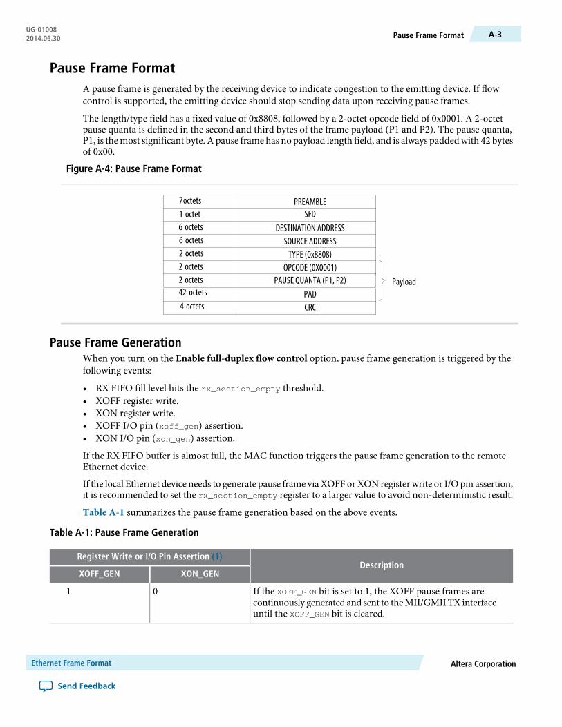
Pause Frame FormatA pause frame is generated by the receiving device to indicate congestion to the emitting device. If flowcontrol is supported, the emitting device should stop sending data upon receiving pause frames.
The length/type field has a fixed value of 0x8808, followed by a 2-octet opcode field of 0x0001. A 2-octetpause quanta is defined in the second and third bytes of the frame payload (P1 and P2). The pause quanta,P1, is themost significant byte. A pause frame has no payload length field, and is always paddedwith 42 bytesof 0x00.
Figure A-4: Pause Frame Format
7octets PREAMBLE1 octet SFD6 octets DESTINATION ADDRESS6 octets SOURCE ADDRESS2 octets
42 octets PADCRC
2 octets2 octets
4 octets
PayloadPAUSE QUANTA (P1, P2)OPCODE (0X0001)TYPE (0x8808)
Pause Frame GenerationWhen you turn on the Enable full-duplex flow control option, pause frame generation is triggered by thefollowing events:
• RX FIFO fill level hits the rx_section_empty threshold.• XOFF register write.• XON register write.• XOFF I/O pin (xoff_gen) assertion.• XON I/O pin (xon_gen) assertion.
If the RX FIFO buffer is almost full, the MAC function triggers the pause frame generation to the remoteEthernet device.
If the local Ethernet device needs to generate pause frame via XOFF orXON register write or I/O pin assertion,it is recommended to set the rx_section_empty register to a larger value to avoid non-deterministic result.
Table A-1 summarizes the pause frame generation based on the above events.
Table A-1: Pause Frame Generation
DescriptionRegister Write or I/O Pin Assertion (1)
XON_GENXOFF_GEN
If the XOFF_GEN bit is set to 1, the XOFF pause frames arecontinuously generated and sent to theMII/GMIITX interfaceuntil the XOFF_GEN bit is cleared.
01
Altera CorporationEthernet Frame Format
Send Feedback
A-3Pause Frame FormatUG-010082014.06.30
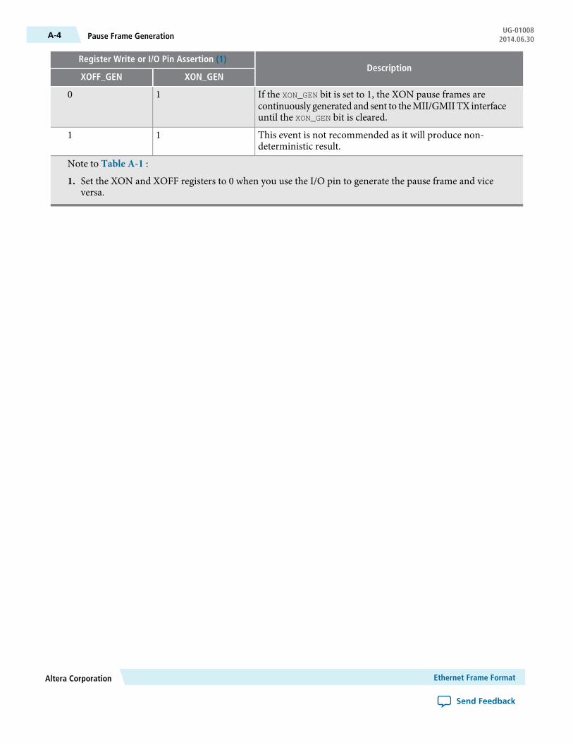
DescriptionRegister Write or I/O Pin Assertion (1)
XON_GENXOFF_GEN
If the XON_GEN bit is set to 1, the XON pause frames arecontinuously generated and sent to theMII/GMIITX interfaceuntil the XON_GEN bit is cleared.
10
This event is not recommended as it will produce non-deterministic result.
11
Note to Table A-1 :
1. Set the XON and XOFF registers to 0 when you use the I/O pin to generate the pause frame and viceversa.
Ethernet Frame FormatAltera Corporation
Send Feedback
UG-01008Pause Frame GenerationA-4 2014.06.30
BSimulation Parameters
2014.06.30
UG-01008 Subscribe Send Feedback
Functionality Configuration ParametersYou can use these parameters to enable or disable specific functionality in the MAC and PCS.
Table B-1: MegaCore Functionality Configuration Parameters
DefaultDescriptionParameter
Supported in configurations that contain the 10/100/1000 Ethernet MAC
100010: Enables MII.
100: Enables MII.
1000: Enables GMII.
ETH_MODE
0Sets the HD_ENA bit in the command_config register. SeeCommand_Config Register (Dword Offset 0x02) onpage 6-7.
HD_ENA
15Sets the pause_quant register. See Base ConfigurationRegisters (Dword Offset 0x00 – 0x17) on page 6-3.
TB_MACPAUSEQ
0Sets the PAUSE_IGNORE bit in the command_configregister. SeeCommand_ConfigRegister (DwordOffset0x02) on page 6-7.
TB_MACIGNORE_PAUSE
0Sets the PAUSE_FWD bit in the command_config register.See Command_Config Register (Dword Offset 0x02)on page 6-7.
TB_MACFWD_PAUSE
0Sets the CRC_FWD bit in the command_config register. SeeCommand_Config Register (Dword Offset 0x02) onpage 6-7.
TB_MACFWD_CRC
0Sets the ADDR_INS bit in the command_config register.See Command_Config Register (Dword Offset 0x02)on page 6-7.
TB_MACINSERT_ADDR
1Sets the PROMIS_EN bit in the command_config register.See Command_Config Register (Dword Offset 0x02)on page 6-7.
TB_PROMIS_ENA
ISO9001:2008Registered
© 2014 Altera Corporation. All rights reserved. ALTERA, ARRIA, CYCLONE, ENPIRION, MAX, MEGACORE, NIOS, QUARTUS and STRATIX wordsand logos are trademarks of Altera Corporation and registered in the U.S. Patent and Trademark Office and in other countries. All otherwords and logos identified as trademarks or service marks are the property of their respective holders as described atwww.altera.com/common/legal.html. Altera warrants performance of its semiconductor products to current specifications in accordance withAltera's standard warranty, but reserves the right to make changes to any products and services at any time without notice. Altera assumesno responsibility or liability arising out of the application or use of any information, product, or service described herein except as expresslyagreed to in writing by Altera. Altera customers are advised to obtain the latest version of device specifications before relying on any publishedinformation and before placing orders for products or services.
www.altera.com
101 Innovation Drive, San Jose, CA 95134

DefaultDescriptionParameter
1Sets the PAD_EN bit in the command_config register. SeeCommand_Config Register (Dword Offset 0x02) onpage 6-7.
TB_MACPADEN
1518Maximum frame length.TB_MACLENMAX
12Sets the tx_ipg_length register. SeeBaseConfigurationRegisters (Dword Offset 0x00 – 0x17) on page 6-3.
TB_IPG_LENGTH
0Sets the mdio_addr0 register. See Base ConfigurationRegisters (Dword Offset 0x00 – 0x17) on page 6-3.
TB_MDIO_ADDR0
1Sets the mdio_addr1 register. See Base ConfigurationRegisters (Dword Offset 0x00 – 0x17) on page 6-3.
TB_MDIO_ADDR1
8Sets the tx_almost_empty register. See BaseConfiguration Registers (Dword Offset 0x00 – 0x17)on page 6-3.
TX_FIFO_AE
10Sets the tx_almost_full register. See BaseConfiguration Registers (Dword Offset 0x00 – 0x17)on page 6-3.
TX_FIFO_AF
8Sets the rx_almost_empty register. See BaseConfiguration Registers (Dword Offset 0x00 – 0x17)on page 6-3.
RX_FIFO_AE
8Sets the rx_almost_full register. See BaseConfiguration Registers (Dword Offset 0x00 – 0x17)on page 6-3.
RX_FIFO_AF
16Sets the tx_section_empty register. See BaseConfiguration Registers (Dword Offset 0x00 – 0x17)on page 6-3.
TX_FIFO_SECTION_EMPTY
16Sets the tx_section_full register. See BaseConfiguration Registers (Dword Offset 0x00 – 0x17)on page 6-3.
TX_FIFO_SECTION_FULL
0Sets the rx_section_empty register. See BaseConfiguration Registers (Dword Offset 0x00 – 0x17)on page 6-3.
RX_FIFO_SECTION_EMPTY
16Sets the rx_section_full register. See BaseConfiguration Registers (Dword Offset 0x00 – 0x17)on page 6-3.
RX_FIFO_SECTION_FULL
9Specifies the first n addresses from MCAST_ADDRESSLIST
from which multicast address is selected.MCAST_TABLEN
Simulation ParametersAltera Corporation
Send Feedback
UG-01008Functionality Configuration ParametersB-2 2014.06.30
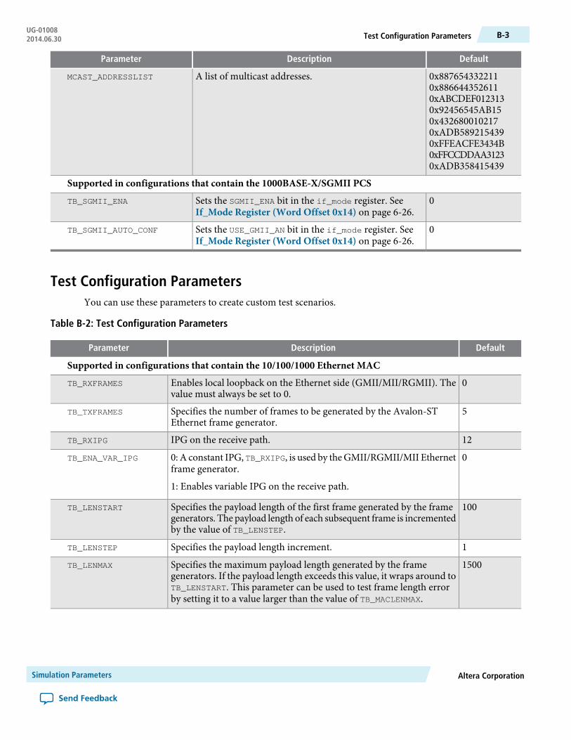
DefaultDescriptionParameter
0x8876543322110x8866443526110xABCDEF0123130x92456545AB150x4326800102170xADB5892154390xFFEACFE3434B0xFFCCDDAA31230xADB358415439
A list of multicast addresses.MCAST_ADDRESSLIST
Supported in configurations that contain the 1000BASE-X/SGMII PCS
0Sets the SGMII_ENA bit in the if_mode register. SeeIf_Mode Register (Word Offset 0x14) on page 6-26.
TB_SGMII_ENA
0Sets the USE_GMII_AN bit in the if_mode register. SeeIf_Mode Register (Word Offset 0x14) on page 6-26.
TB_SGMII_AUTO_CONF
Test Configuration ParametersYou can use these parameters to create custom test scenarios.
Table B-2: Test Configuration Parameters
DefaultDescriptionParameter
Supported in configurations that contain the 10/100/1000 Ethernet MAC
0Enables local loopback on the Ethernet side (GMII/MII/RGMII). Thevalue must always be set to 0.
TB_RXFRAMES
5Specifies the number of frames to be generated by the Avalon-STEthernet frame generator.
TB_TXFRAMES
12IPG on the receive path.TB_RXIPG
00: A constant IPG, TB_RXIPG, is used by theGMII/RGMII/MII Ethernetframe generator.
1: Enables variable IPG on the receive path.
TB_ENA_VAR_IPG
100Specifies the payload length of the first frame generated by the framegenerators. The payload length of each subsequent frame is incrementedby the value of TB_LENSTEP.
TB_LENSTART
1Specifies the payload length increment.TB_LENSTEP
1500Specifies the maximum payload length generated by the framegenerators. If the payload length exceeds this value, it wraps around toTB_LENSTART. This parameter can be used to test frame length errorby setting it to a value larger than the value of TB_MACLENMAX.
TB_LENMAX
Altera CorporationSimulation Parameters
Send Feedback
B-3Test Configuration ParametersUG-010082014.06.30
DefaultDescriptionParameter
10: Disables padding.
1: If the length of frames generated by the GMII/RGMII/MII Ethernetframe generator is less than the minimum frame length (64 bytes), thegenerator inserts padding bytes to the frames tomake up theminimumlength.
TB_ENA_PADDING
00: Only basic frames are generated.
1: Enables VLAN frames generation. This value specifies the numberof basic frames generated before a VLAN frame is generated followedby a stacked VLAN frame.
TB_ENA_VLAN
0Specifies the number of packets to be read from the receive FIFO beforereading is suspended. You can use this parameter to test FIFO overflowand flow control.
TB_STOPREAD
1000Specifies the number of clock cycles before the Avalon-ST monitorstops reading from the receive FIFO.
TB_HOLDREAD
00: Normal behavior.
1: Drives theAvalon-ST error signal high to simulate erroneous framestransmission.
TB_TX_FF_ERR
0Specifies the number of clock cycles from the start of simulation beforethe xoff_gen signal is driven.
TB_TRIGGERXOFF
0Specifies the number of clock cycles from the start of simulation beforethe xon_gen signal is driven high.
TB_TRIGGERXON
0Specifies which frame is received with collision. Valid in fast Ethernetand half-duplex mode only.
RX_COL_FRM
0Specifies which nibble within the frame collision occurs.RX_COL_GEN
0Specifies which frame is transmitted with a collision. Valid in fastEthernet and half-duplex mode only.
TX_COL_FRM
0Specifies which nibble within the frame collision occurs on the transmitpath.
TX_COL_GEN
0Specifies the number of consecutive collisions during retransmission.TX_COL_NUM
0Specifies the delay, in nibbles, between collision and retransmission.TX_COL_DELAY
10: GMII frame generator does not respond to pause frames.
1: Enables flow control in the GMII frame generator.
TB_PAUSECONTROL
0Enable / Disable MDIO simulation.TB_MDIO_SIMULATION
Supported in configurations that contain the 1000BASE-X/SGMII PCS
00: Disables half-duplex mode.
1: Enables half-duplex mode.
TB_SGMII_HD
Simulation ParametersAltera Corporation
Send Feedback
UG-01008Test Configuration ParametersB-4 2014.06.30
DefaultDescriptionParameter
10: Disables gigabit operation.
1: Enables gigabit operation.
TB_SGMII_1000
00: Disables 100 Mbps operation.
1: Enables 100 Mbps operation.
TB_SGMII_100
00: Disables 10 Mbps operation.
1: Enables 10 Mbps operation.
TB_SGMII_10
00: Disables error generation.
1: Enables error generation.
TB_TX_ERR
Altera CorporationSimulation Parameters
Send Feedback
B-5Test Configuration ParametersUG-010082014.06.30

CTime-of-Day (ToD) Clock
2014.06.30
UG-01008 Subscribe Send Feedback
The Time-of-Day (ToD) clock provides a stream of timestamps for the IEEE 1588v2 feature.
ToD Clock Features• Provides a stream of 64-bit and 96-bit timestamps.
• The 64-bit timestamp has 48-bit nanosecond field and 16-bit fractional nanosecond field.• The 96-bit timestamphas 48-bit second field, 32-bit nanosecond field, and 16-bit fractional nanosecond
field.
• Runs at 125-MHz for the Triple-Speed Ethernet MegaCore function.• Supports coarse adjustment and fine adjustments through clean frequency adjustment.• Supports period adjustment for frequency control using the Period register.• Supports offset adjustment using the AdjustPeriod register.
ToD Clock Device Family Support
Table C-1: Device Family Support
SupportDevice Family
PreliminaryArria V GX/GT/GZ/SoC
PreliminaryCyclone V GX/GT/SoC
PreliminaryStratix V GX/GT
No supportOther device families
ToD Clock Performance and Resource UtilizationTable C-2 provides the estimated resource utilization and performance of the ToD clock for the Stratix Vdevice family. The estimates are obtained by compiling the Triple-Speed Ethernet MegaCore function usingthe Quartus II software targeting a Stratix V GX (5SGXMA7N3F45C3) device with speed grade -3.
ISO9001:2008Registered
© 2014 Altera Corporation. All rights reserved. ALTERA, ARRIA, CYCLONE, ENPIRION, MAX, MEGACORE, NIOS, QUARTUS and STRATIX wordsand logos are trademarks of Altera Corporation and registered in the U.S. Patent and Trademark Office and in other countries. All otherwords and logos identified as trademarks or service marks are the property of their respective holders as described atwww.altera.com/common/legal.html. Altera warrants performance of its semiconductor products to current specifications in accordance withAltera's standard warranty, but reserves the right to make changes to any products and services at any time without notice. Altera assumesno responsibility or liability arising out of the application or use of any information, product, or service described herein except as expresslyagreed to in writing by Altera. Altera customers are advised to obtain the latest version of device specifications before relying on any publishedinformation and before placing orders for products or services.
www.altera.com
101 Innovation Drive, San Jose, CA 95134

Table C-2: Stratix V Performance and Resource Utilization
Memory (M20KBlocks/MLAB
Bits)
Logic RegistersCombinationalALUTs
FIFO BufferSize (Bits)
SettingsMegaCore Function
0/01,1203780DefaultTOD Clock
ToD Clock Parameter Setting
Table C-3: ToD Clock Configuration Parameters
DescriptionValueName
4-bit value that defines the reset valuefor PERIOD_NS. For Triple-SpeedEthernet MegaCore function, set thevalue to 0x0008.
The default value is 0x0006.
Between 0 and 0x000FDEFAULT_NSEC_PERIOD
16-bit value that defines the reset valuefor PERIOD_FNS. For Triple-SpeedEthernet MegaCore function, set thevalue to 0x0000.
The default value is 0x6666.
Between 0 and 0xFFFFDEFAULT_FNSEC_PERIOD
4-bit value that defines the reset valuefor ADJPERIOD_NS.
The default value is 0x0006.
Between 0 and 0x000FDEFAULT_NSEC_ADJPERIOD
16-bit value that defines the reset valuefor PERIOD_FNS.
The default value is 0x6666.
Between 0 and 0xFFFFDEFAULT_FNSEC_ADJPERIOD
Time-of-Day (ToD) ClockAltera Corporation
Send Feedback
UG-01008ToD Clock Parameter SettingC-2 2014.06.30
ToD Clock Interface SignalsFigure C-1: Time-of-Day Clock Interface Signals
ToD Clock
Avalon-MMControl
InterfaceSignals
csr_readdata[] 32
csr_read
clk
rst_n
csr_write
csr_writedata[]32
csr_address[]4
time_of_day_96[] 96
time_of_day_64[]64
csr_readdata[] 32
time_of_day_96b_load_valid
period_clk
time_of_day_96b_load_data[]Avalon-STTransmitInterfaceSignals time_of_day_64b_load_valid
time_of_day_64b_load_data[]64
96
ToD Clock Avalon-MM Control Interface Signals
Table C-4: Avalon-MM Control Interface Signals for ToD Clock
DescriptionWidthDirectionSignal
Use this bus to specify the register address you wantto read from or write to.
2Inputcsr_address[]
Assert this signal to request a read.1Inputcsr_read
Carries the data read from the specified register.32Outputcsr_readdata[]
Assert this signal to request a write.1Inputcsr_write
Carries the data to be written to the specified register.32Inputcsr_writedata[]
Register access reference clock.1Inputclk
Assert this active low signal to reset the ToD clock.1Inputrst_n
Altera CorporationTime-of-Day (ToD) Clock
Send Feedback
C-3ToD Clock Interface SignalsUG-010082014.06.30
ToD Clock Avalon-ST Transmit Interface Signals
Table C-5: Avalon-ST Transmit Interface Signals for ToD Clock
DescriptionWidthDirectionSignal
Timestamp from the ToD clock
• Bits 0 to 15: 16-bit fractional nanosecondfield
• Bits 16 to 63: 48-bit nanosecond field
64Outputtime_of_day_64b[]
Timestamp from the ToD clock
• Bits 0 to 15: 16-bit fractional nanosecondfield
• Bits 16 to 47: 32-bit nanosecond field• Bits 48 to 95: 48-bit second field
96Outputtime_of_day_96b[]
Indicates that the synchronized ToD is valid.Every time you assert this signal, the synchro-nized ToD is loaded into the ToD clock. Assertthis signal for only one clock cycle.
1Inputtime_of_day_96b_load_valid
Loads 96-bit synchronized ToD from masterToD clock to slave ToD clock within 1 clockcycle.
• Bits 0 to 15: 16-bit fractional nanosecondfield
• Bits 16 to 63: 32-bit nanosecond field• Bits 64 to 95: 48-bit second field
96Inputtime_of_day_96b_load_data[]
Indicates that the synchronized ToD is valid.Every time you assert this signal, the synchro-nized ToD is loaded into the ToD clock. Assertthis signal for only one clock cycle.
1Inputtime_of_day_64b_load_valid
Loads 64-bit synchronized ToD from masterToD clock to slave ToD clock within 1 clockcycle.
• Bits 0 to 15: 16-bit fractional nanosecondfield
• Bits 16 to 63: 48-bit nanosecond field
64Inputtime_of_day_64b_load_data[]
Clock for the ToD clock. The clock must be inthe same clock domain as tx_time_of_day andrx_time_of_day in the MAC function.
1Inputperiod_clk
Assert this signal to reset period_clk to thesame clock domain as tx_time_of_day andrx_time_of_day in the MAC function.
1Inputperiod_rst_n
Time-of-Day (ToD) ClockAltera Corporation
Send Feedback
UG-01008ToD Clock Avalon-ST Transmit Interface SignalsC-4 2014.06.30

ToD Clock Configuration Register Space
Table C-6: ToD Clock Registers
HWReset
DescriptionR/WNameDword
Offset
0x0• Bits 0 to 15: High-order 16-bit second field.• Bits 16 to 31: Not used.
RWSecondsH0x00
0x0Bits 0 to 32: Low-order 32-bit second field.RWSecondsL0x01
0x0Bits 0 to 32: 32-bit nanosecond field.RWNanoSec0x02
—Reserved for future use—Reserved0x03
nThe period for the frequency adjustment.
• Bits 0 to 15: Period in fractional nanosecond(PERIOD_FNS).
• Bits 16 to 24: Period in nanosecond (PERIOD_NS).
• Bits 25 to 31: Not used.
The default value for the period depends on thefMAX of the MAC function. For example, if fMAX =125-MHz, the period is 8-ns (PERIOD_NS = 0x0008and PERIOD_FNS = 0x0000).
RWPeriod0x04
0x0The period for the offset adjustment.
• Bits 0 to 15: Period in fractional nanosecond(ADJPERIOD_FNS).
• Bits 16 to 24: Period in nanosecond(ADJPERIOD_NS).
• Bits 25 to 31: Not used.
RWAdjustPeriod0x05
0x06Bits 0 to 19: The number of AdjustPeriod clockcycles used during offset adjustment.
Bits 20 to 31: Not used.
RWAdjustCount0x06
Altera CorporationTime-of-Day (ToD) Clock
Send Feedback
C-5ToD Clock Configuration Register SpaceUG-010082014.06.30
HWReset
DescriptionR/WNameDword
Offset
0x0The drift of ToD adjusted periodically by addinga correction value as configured in this registerspace.
• Bits 0 to 15: Adjustment value in fractionalnanosecond (DRIFT_ADJUST_FNS). This valueis added into the current ToD during theadjustment. The default value is 0.
• Bits 16 to 19: Adjustment value in nanosecond(DRIFT_ADJUST_NS). This value is added intothe current ToD during the adjustment. Thedefault value is 0.
• Bits 20 to 32: Not used.
RWDriftAdjust0x1C
0x0The count of clock cycles for each ToD’s driftadjustment to take effect.
• Bits 0 to 15: The number of clock cycles(ADJUST_RATE). The ToD adjustment happensonce after every period in number of clockcycles as indicated by this register space.
• Bits 16 to 32: Not used.
RWDriftAdjustRate0x20
Adjusting ToD Clock DriftYou can use the DriftAdjust and DriftAdjustRate registers to correct any drift in the ToD clock.
In the case of a ToD for 10G with period of 6.4ns, the nanosecond field is converted directly to PERIOD_NS
while the fractional nanosecond need to be multiplied with 216 or 65536 in order to convert to PERIOD_FNS.This results in 0x6 PERIOD_NS and 0x6666.4 PERIOD_FNS.
PERIOD_NS only accepts 0x6666 and ignores 0x0000.4, which in turn would cause some inaccuracy in theconfigured period. This inaccuracy causes the ToD to drift from the actual time as much as 953.67 ns aftera period of 1 second. You would notice that after every 5 cycles, 0x0000.4 accumulates to 0x0002. If the TODis able to add 0x0002 of fractional nanosecond into the ToD once after every period of 5 cycles, then it willcorrect the drift.
Therefore, for the 10G case, DRIFT_ADJUST_NS is now configured to 0x0, DRIFT_ADJUST_FNS is configuredto 0x0002 and ADJUST_RATE is configured to 0x5.
Time-of-Day (ToD) ClockAltera Corporation
Send Feedback
UG-01008Adjusting ToD Clock DriftC-6 2014.06.30
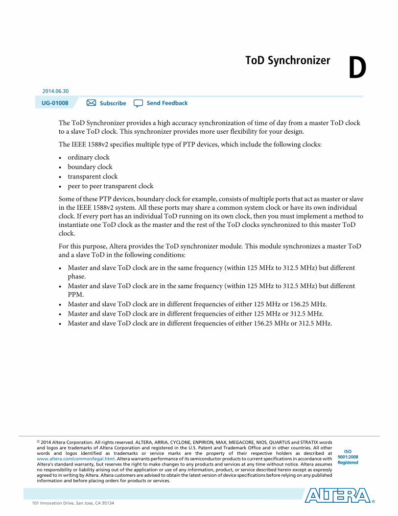
DToD Synchronizer
2014.06.30
UG-01008 Subscribe Send Feedback
The ToD Synchronizer provides a high accuracy synchronization of time of day from a master ToD clockto a slave ToD clock. This synchronizer provides more user flexibility for your design.
The IEEE 1588v2 specifies multiple type of PTP devices, which include the following clocks:
• ordinary clock• boundary clock• transparent clock• peer to peer transparent clock
Some of these PTP devices, boundary clock for example, consists of multiple ports that act as master or slavein the IEEE 1588v2 system. All these ports may share a common system clock or have its own individualclock. If every port has an individual ToD running on its own clock, then you must implement a method toinstantiate one ToD clock as the master and the rest of the ToD clocks synchronized to this master ToDclock.
For this purpose, Altera provides the ToD synchronizer module. This module synchronizes a master ToDand a slave ToD in the following conditions:
• Master and slave ToD clock are in the same frequency (within 125 MHz to 312.5 MHz) but differentphase.
• Master and slave ToD clock are in the same frequency (within 125 MHz to 312.5 MHz) but differentPPM.
• Master and slave ToD clock are in different frequencies of either 125 MHz or 156.25 MHz.• Master and slave ToD clock are in different frequencies of either 125 MHz or 312.5 MHz.• Master and slave ToD clock are in different frequencies of either 156.25 MHz or 312.5 MHz.
ISO9001:2008Registered
© 2014 Altera Corporation. All rights reserved. ALTERA, ARRIA, CYCLONE, ENPIRION, MAX, MEGACORE, NIOS, QUARTUS and STRATIX wordsand logos are trademarks of Altera Corporation and registered in the U.S. Patent and Trademark Office and in other countries. All otherwords and logos identified as trademarks or service marks are the property of their respective holders as described atwww.altera.com/common/legal.html. Altera warrants performance of its semiconductor products to current specifications in accordance withAltera's standard warranty, but reserves the right to make changes to any products and services at any time without notice. Altera assumesno responsibility or liability arising out of the application or use of any information, product, or service described herein except as expresslyagreed to in writing by Altera. Altera customers are advised to obtain the latest version of device specifications before relying on any publishedinformation and before placing orders for products or services.
www.altera.com
101 Innovation Drive, San Jose, CA 95134

ToD Synchronizer BlockFigure D-1: Connection between ToD Synchronizer, Master ToD, Slave ToD, and Sampling Clock PLL
Slave ToD
time_of_day_96b_load_valid
time_of_day_96b_load_data
period_rst_n
period_clk
ToD Synchronizer
tod_master_data
reset_master
clk_master
tod_slave_validSynchronization valid
Synchronization ToDtod_slave_data
reset_slave
clk_slave
clk_sampling
start_tod_syncMaster ToD
PLL
time_of_day_96b Master ToD
1’b1
Sampling clock
Master reset
Slave reset
Master clock
Slave clock
period_rst_n
period_clk
The components:
• Master TOD clock domain—consists of three interfaces: clk_master, reset_master, andtod_master_data.
• Slave TOD clock domain—consists of five interfaces: clk_slave, reset_slave, tod_slave_valid,tod_slave_data, and start_tod_sync.
• Sampling clock PLL—consists of the clk_domain interface.
TheTod synchronizermodule synchronizes themaster ToD clock domainwith the slave ToD clock domain.The dual-clock FIFO in the Tod synchronizer block takes in the time of day from the master ToD clockdomain and transfers it to the slave ToD clock domain. The slave ToD then will load the synchronized timeof day into its own internal counter, which then increments based on the new value.
As the ToD transfer is in progress, the master ToD domain keeps incrementing. When the ToD reaches theslave ToD clock domain and is ready to be loaded, it is much slower than the master ToD. To achieve highaccuracy synchronization, the latency caused by the transfer must be reflected in the synchronized ToD.
The sampling clock PLL (clk_sampling) samples the FIFO fill level and calculates the latency through theFIFO. For better accuracy, the sampling clock must be derived from the master (clk_master) or slave(clk_slave) clock domain using a PLL.
If you use the recommended sampling clock frequency, the Tod synchronizer module takes 64 clock cyclesof sampling clock for every newly synchronized ToDto be valid at the output port.
Altera recommends that you use the following sampling clock frequencies:
• 1G master and slave—(64/63)*125 MHz• 10G master and slave—(64/63)*156.25 MHz• 1G master and 10G slave—(16/63)*125 MHz or (64/315)*156.25 MHz• 10G master and 1G slave—(16/63)*125 MHz or (64/315)*156.25 MHz• 10G (312.5 Mhz) master and slave—(64/63)*312.5 MHz
ToD SynchronizerAltera Corporation
Send Feedback
UG-01008ToD Synchronizer BlockD-2 2014.06.30
• 1G master and 10G (312.5 Mhz) slave—(32/63)*125 MHz or (64/315)*312.5 MHz• 10G (156.25 MHz) master and 10G (312.5 Mhz) slave—(64/63)*156.25 MHz or (32/63)*312.5 MHz
Table D-1: Settings to Achieve The Recommended Factors for Stratix V PLL
32/6364/31516/6364/63Settings
32641664M-Counter
03210321N-Counter
21152103C-Counter
ToD Synchronizer Parameter Settings
Table D-2: ToD Synchronizer Configuration Parameters
DescriptionValueName
Value that defines the time of day format thatthis block is synchronizing.
The default value is 1.
• 1: 96-bits format (32 bits seconds, 48 bitsnanosecond and 16 bits fractionalnanosecond)
• 0: 64-bits format (48 bits nanosecond and 16bits fractional nanoseconds).
Between 0 and 1TOD_MODE
Value that defines types of synchronization.
The default value is 1.
• 0: Master clock frequency is 125MHz (1G)while slave is 156.25MHz (10G).
• 1: Master clock frequency is 156.25MHz(10G) while slave is 125MHz (1G).
• 2: Master and slave are same in the samefrequency; can be in different ppm or phase.When you select this mode, specify theperiod of master and slave through thePERIOD_NSEC andPERIOD_FNSECparameters.
• 3: Master clock frequency is 156.25MHz(10G) while slave is 312.5MHz (10G).
• 4:Master clock frequency is 312.5MHz (10G)while slave is 156.25MHz (10G).
• 5: Master clock frequency is 125MHz (1G)while slave is 312.5MHz (10G).
• 6:Master clock frequency is 312.5MHz (10G)while slave is 125MHz (1G).
Between 0 and 6SYNC_MODE
Altera CorporationToD Synchronizer
Send Feedback
D-3ToD Synchronizer Parameter SettingsUG-010082014.06.30

DescriptionValueName
A 4-bit value that defines the reset value for ananosecond of period.
The default value is 4'h6 to capture 6.4ns for156.25MHz frequency. For 125MHz frequency(1G), set this parameter to 4'h8.
Between 0 and 4’hFPERIOD_NSEC
A 4-bit value that defines the reset value for afractional nanosecond of period.
The default value is 16'h6666 to capture 0.4nsof 6.4ns for 156.25 MHz frequency. For 125MHz frequency (1G), set this parameter to 16'h0.
Between 0 and 16’hFFFFPERIOD_FNSEC
ToD Synchronizer Signals
ToD Synchronizer Common Clock and Reset Signals
Table D-3: Clock and Reset Signals for the ToD Synchronizer
DescriptionWidthDirectionSignal
Clock from master ToD domain.1Inputclk_master
Reset signal that is synchronized to the masterToD clock domain.
1Inputreset_master
Clock from slave ToD domain.1Inputclk_slave
Reset signal that is synchronized to the slaveToD clock domain.
1Inputreset_slave
Sampling clock to measure the latency acrossthe ToD Synchronizer.
1Inputclk_sampling
ToD Synchronizer Interface Signals
Table D-4: Interface Signals for the ToD Synchronizer
DescriptionWidthDirectionSignal
Assert this signal to start the ToD synchroniza-tion process. When this signal is asserted, thesynchronization process continues and the timeof day from the master ToD clock domain willbe repeatedly synchronized with the slave ToDclock domain.
1Inputstart_tod_sync
ToD SynchronizerAltera Corporation
Send Feedback
UG-01008ToD Synchronizer SignalsD-4 2014.06.30

DescriptionWidthDirectionSignal
This signal carries the 64-bit or 96-bit formatdata for the time of day from the master ToD.The width of this signal is determined by theTOD_MODE parameter.
1Inputtod_master_data
This signal indicates that the tod_data_slavesignal is valid and ready to be loaded into theslave ToD clock in the following cycle.
This signal will only be high for 1 cycle everytime a new time of day is successfully synchro-nized to the slave clock domain.
tod_slave_valid
This signal carries the 64-bit or 96-bit formatsynchronized time of day that is ready to beloaded into the slave clock domain. The widthof this signal is determined by the TOD_MODEparameter.
The synchronized time of day will be 1 slaveclock period bigger than the master ToDbecause it takes 1 slave clock cycle to load thisdata into the slave ToD.
1Inputtod_slave_data[n-1:0]
Altera CorporationToD Synchronizer
Send Feedback
D-5ToD Synchronizer Interface SignalsUG-010082014.06.30
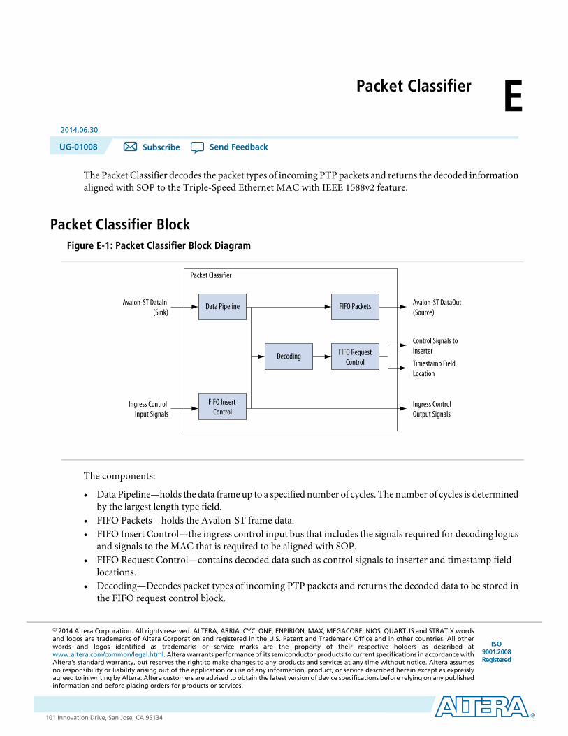
EPacket Classifier
2014.06.30
UG-01008 Subscribe Send Feedback
The Packet Classifier decodes the packet types of incoming PTP packets and returns the decoded informationaligned with SOP to the Triple-Speed Ethernet MAC with IEEE 1588v2 feature.
Packet Classifier BlockFigure E-1: Packet Classifier Block Diagram
Packet Classifier
Avalon-ST DataIn(Sink)
Ingress ControlInput Signals
Ingress ControlOutput Signals
Avalon-ST DataOut(Source)
Control Signals toInserter
Timestamp FieldLocation
Data Pipeline FIFO Packets
FIFO InsertControl
FIFO RequestControl
Decoding
The components:
• Data Pipeline—holds the data frame up to a specified number of cycles. The number of cycles is determinedby the largest length type field.
• FIFO Packets—holds the Avalon-ST frame data.• FIFO Insert Control—the ingress control input bus that includes the signals required for decoding logics
and signals to the MAC that is required to be aligned with SOP.• FIFO Request Control—contains decoded data such as control signals to inserter and timestamp field
locations.• Decoding—Decodes packet types of incoming PTP packets and returns the decoded data to be stored in
the FIFO request control block.
ISO9001:2008Registered
© 2014 Altera Corporation. All rights reserved. ALTERA, ARRIA, CYCLONE, ENPIRION, MAX, MEGACORE, NIOS, QUARTUS and STRATIX wordsand logos are trademarks of Altera Corporation and registered in the U.S. Patent and Trademark Office and in other countries. All otherwords and logos identified as trademarks or service marks are the property of their respective holders as described atwww.altera.com/common/legal.html. Altera warrants performance of its semiconductor products to current specifications in accordance withAltera's standard warranty, but reserves the right to make changes to any products and services at any time without notice. Altera assumesno responsibility or liability arising out of the application or use of any information, product, or service described herein except as expresslyagreed to in writing by Altera. Altera customers are advised to obtain the latest version of device specifications before relying on any publishedinformation and before placing orders for products or services.
www.altera.com
101 Innovation Drive, San Jose, CA 95134
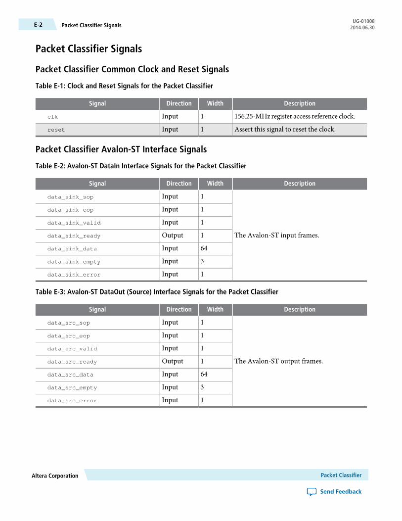
Packet Classifier Signals
Packet Classifier Common Clock and Reset Signals
Table E-1: Clock and Reset Signals for the Packet Classifier
DescriptionWidthDirectionSignal
156.25-MHz register access reference clock.1Inputclk
Assert this signal to reset the clock.1Inputreset
Packet Classifier Avalon-ST Interface Signals
Table E-2: Avalon-ST DataIn Interface Signals for the Packet Classifier
DescriptionWidthDirectionSignal
The Avalon-ST input frames.
1Inputdata_sink_sop
1Inputdata_sink_eop
1Inputdata_sink_valid
1Outputdata_sink_ready
64Inputdata_sink_data
3Inputdata_sink_empty
1Inputdata_sink_error
Table E-3: Avalon-ST DataOut (Source) Interface Signals for the Packet Classifier
DescriptionWidthDirectionSignal
The Avalon-ST output frames.
1Inputdata_src_sop
1Inputdata_src_eop
1Inputdata_src_valid
1Outputdata_src_ready
64Inputdata_src_data
3Inputdata_src_empty
1Inputdata_src_error
Packet ClassifierAltera Corporation
Send Feedback
UG-01008Packet Classifier SignalsE-2 2014.06.30

Packet Classifier Ingress Control Signals
Table E-4: Ingress Control Signals for the Packet Classifier
DescriptionWidthDirectionSignal
96-bit format of ingress timestamp thatholds data so that the output can alignwith the start of an incoming packet.
96Inputtx_etstamp_ins_ctrl_in_ingress_
timestamp_96b
64-bit format of ingress timestamp thatholds data so that the output can alignwith the start of an incoming packet.
64Inputtx_etstamp_ins_ctrl_in_ingress_
timestamp_64b
96-bit format of ingress timestamp thatholds data so that the output can alignwith the start of an outgoing packet.
96Outputtx_etstamp_ins_ctrl_out_ingress_
timestamp_96b
64-bit format of ingress timestamp thatholds data so that the output can alignwith the start of an outgoing packet.
64Outputtx_etstamp_ins_ctrl_out_ingress_
timestamp_64b
Assert this signal when timestamp isrequired for the particular frame. Thissignal must be aligned to the start of anincoming packet.
1Inputtx_egress_timestamp_request_in_
valid
A width-configurable fingerprint thatcorrelates timestamps for incomingpackets.
4Inputtx_egress_timestamp_request_in_
fingerprint
Assert this signal when timestamp isrequired for the particular frame. Thissignal must be aligned to the start of anoutgoing packet.
1Outputtx_egress_timestamp_request_out_
valid
A width-configurable fingerprint thatcorrelates timestamps for outgoingpackets.
4Outputtx_egress_timestamp_request_out_
fingerprint
Determines the clock mode.
• 00: Ordinary clock• 01: Boundary clock• 10: End-to-end transparent clock• 11: Peer-to-peer transparent clock
2Inputclock mode
Indicates whether or not a packetcontains CRC.
• 1: Packet contains CRC• 0: Packet does not contain CRC
1Inputpkt_with_crc
Altera CorporationPacket Classifier
Send Feedback
E-3Packet Classifier Ingress Control SignalsUG-010082014.06.30

DescriptionWidthDirectionSignal
Indicates the update for residence time.
• 1: Allows update for residence timebased on decoded results.
• 0: Prevents update for residence time.When this signal is deasserted, tx_etstamp_ins_ctrl_out_residence_
time_update also gets deasserted.
1Inputtx_etstamp_ins_ctrl_in_residence_
time_update
Format of the timestamp to be used forcalculating residence time. This signalmust be aligned to the start of anincoming packet.
• 1: 64-bit timestamp format• 0: 96-bit timestamp format
1Inputtx_etstamp_ins_ctrl_in_residence_
time_calc_format
Format of the timestamp to be used forcalculating residence time. This signalmust be aligned to the start of anoutgoing packet.
• 1: 64-bit timestamp format• 0: 96-bit timestamp format
1Outputtx_etstamp_ins_ctrl_out_residence_
time_calc_format
Packet Classifier Control Insert SignalsThese signals must be aligned to the start of a packet.
Table E-5: Control Insert Signals for the Packet Classifier
DescriptionWidthDirectionSignal
Assert this signal to set the checksumfield.
1Outputtx_etstamp_ins_ctrl_out_checksum_
zero
Assert this signal to correct the packetchecksum by updating the checksumcorrection specified by tx_etstamp_ins_ctrl_out_offset_checksum_
correction.
1Outputtx_etstamp_ins_ctrl_out_checksum_
correct
The timestamp format of the framewhere the timestamp is inserted.
1Outputtx_etstamp_ins_ctrl_out_timestamp_
format
Assert this signal to insert timestampinto the associated frame.
1Outputtx_etstamp_ins_ctrl_out_timestamp_
insert
Assert this signal to add the residencetime into the correction field of the PTPframe.
1Outputtx_etstamp_ins_ctrl_out_residence_
time_update
Packet ClassifierAltera Corporation
Send Feedback
UG-01008Packet Classifier Control Insert SignalsE-4 2014.06.30

Packet Classifier Timestamp Field Location SignalsThese signals must be aligned to the start of a packet.
Table E-6: Timestamp Field Location Signals for the Packet Classifier
DescriptionWidthDirectionSignal
Indicates the location of the timestampfield.
16Outputtx_etstamp_ins_ctrl_out_offset_
timestamp
Indicates the location of the correctionfield.
16Outputtx_etstamp_ins_ctrl_out_offset_
correction_field
Indicates the location of the checksumfield.
16Outputtx_etstamp_ins_ctrl_out_offset_
checksum_field
Indicates the location of the checksumcorrector field.
16Outputtx_etstamp_ins_ctrl_out_offset_
checksum_correction
Altera CorporationPacket Classifier
Send Feedback
E-5Packet Classifier Timestamp Field Location SignalsUG-010082014.06.30

FAdditional Information
2014.06.30
UG-01008 Subscribe Send Feedback
Additional information about the document and Altera.
ISO9001:2008Registered
© 2014 Altera Corporation. All rights reserved. ALTERA, ARRIA, CYCLONE, ENPIRION, MAX, MEGACORE, NIOS, QUARTUS and STRATIX wordsand logos are trademarks of Altera Corporation and registered in the U.S. Patent and Trademark Office and in other countries. All otherwords and logos identified as trademarks or service marks are the property of their respective holders as described atwww.altera.com/common/legal.html. Altera warrants performance of its semiconductor products to current specifications in accordance withAltera's standard warranty, but reserves the right to make changes to any products and services at any time without notice. Altera assumesno responsibility or liability arising out of the application or use of any information, product, or service described herein except as expresslyagreed to in writing by Altera. Altera customers are advised to obtain the latest version of device specifications before relying on any publishedinformation and before placing orders for products or services.
www.altera.com
101 Innovation Drive, San Jose, CA 95134

Document Revision History
ChangesVersionDate
• Added a link to the Altera website that provides the latest device supportinformation for Altera IP.
• Added a note in PCS/Transceiver Options on page 3-5—You mustconfigure theArria 10TransceiverATXPLL output clock frequency to 1250.0MHzwhenusing theArria 10TransceiverNative PHYwith theTriple-SpeedEthernet IP core.
• Added MAC Error Correction Code on page 4-19 section.• Added new support configuration for IEEE 1588v2 feature.• Updated the tx_period and rx_period register bits in IEEE1588v2 Feature
(Dword Offset 0xD0 – 0xD6) on page 6-16.• Updated the timing adjustment for the IEEE 1588v2 feature PMA delay in
IEEE 1588v2 Feature PMA Delay on page 6-17.• Revised the control interface signal names to reg_rd, reg_data_in, reg_
wr, reg_busy, and reg_addr in MAC Control Interface Signals on page7-3.
• Added ECC status signals in ECC Status Signals on page 7-11 and ECCStatus Signals on page 7-19.
• Added Arria 10 Transceiver Native PHY signals in Arria 10 TransceiverNative PHY Signals on page 7-18.
• Added Transceiver Native PHY signal in Transceiver Native PHY Signalon page 7-23.
• Updated the following the signal diagrams:
• 10/100/1000 Ethernet MAC Signals• 1000BASE-X/SGMII PCS Function Signals• 10/100/1000 Ethernet MAC with 1000BASE-X/SGMII PCS Signals• 10/100/1000 Multiport Ethernet MAC Function without Internal FIFO
Buffers, with IEEE1588v2, 1000BASE-X/SGMII PCS andEmbeddedPMASignals
• Added IEEE 1588v2 feature PHYpath delay interface signals in IEEE1588v2PHY Path Delay Interface Signals on page 7-33.
• Updated the Period and AdjustPeriod register bits in ToD ClockConfiguration Register Space on page 14-5.
• Added two new conditions that the ToD synchronizer module supports inToD Synchronizer chapter.
• Added three new recommended sampling clock frequencies in ToDSynchronizer chapter.
• Added a new setting of 32/63 in ToD Synchronizer Block on page 15-2.• Updated the SYNC_MODE parameter value and description in ToD Synchro-
nizer Parameter Settings on page 15-3.
14.0June 2014
Additional InformationAltera Corporation
Send Feedback
UG-01008Document Revision HistoryF-2 2014.06.30

ChangesVersionDate
• Added support for Arria 10 device.• Added device family support list for IEEE 1588v2 variant.• Updated the PCS/Transceiver options parameters in PCS/Transceiver
Options on page 3-5.• Updated the bit order in Table F-16 , Table F-17 and Table F-19.• Added information on how to view all the signal names when implementing
the IP in Qsys in Interface Signals.• Added a section about exposed ports in the new user interface in Design
Considerations.
13.1December2013
Altera CorporationAdditional Information
Send Feedback
F-3Document Revision HistoryUG-010082014.06.30

ChangesVersionDate
• Updated the MegaWizard Plug-In Manager flow in Getting Started withAltera IP Cores.
• Added information about generating a design example and simulationtestbench in Generating a Design Example or Simulation Model on page2-7.
• Updated the list of Quartus II generated files.• Added information about the recommended pin assignments in Design
Constraint File No Longer Generated on page 2-10.• Updated the MegaCore parameter names and description in Parameter
Settings• Updated the IEEE 1588v2 feature list in Functional Description.• Updated the SGMII auto-negotiation description inFunctionalDescription.• Added information about the IEEE1588v2 feature PMAdelay in IEEE1588v2
Feature PMA Delay on page 6-17.• Updated the Multiport Ethernet MAC with IEEE 1588v2, 1000BASE-X/
SGMII PCS and Embedded PMA Signals in Figure F-6.• Updated the IEEE 1588v2 timestamp signal names in Interface Signals.• Added timing diagrams for IEEE 1588v2 timestamp signals in Interface
Signals.• Added a section about migrating existing design to the Quartus II software
new MegaCore user interface in Design Considerations.• UpdatedTimingConstraints chapter, to describe the new timing constraint
files and the recommended clock input frequency for eachMegaCore Functionvariant.
• Added information about the simulation model files generated using IEEEsimulation encryption in Simulation Model Files on page 10-5.
• Updated the jumbo frames file directory in Using Jumbo Frames on page11-4.
• Updated the ToD configuration parameters inToDClockParameter Settingon page 14-2 and ToD interface signals in Figure D–1 , ToDClock Avalon-ST Transmit Interface Signals on page 14-4 and ToD Clock Avalon-MMControl Interface Signals on page 14-3.
• Added information to describe the ToD’s drift adjustment inAdjustingToDClock Drift on page 14-6.
• Added ToD Synchronizer and Packet Classifier chapters.• Removed SOPC Builder information.
13.0May 2013
Additional InformationAltera Corporation
Send Feedback
UG-01008Document Revision HistoryF-4 2014.06.30
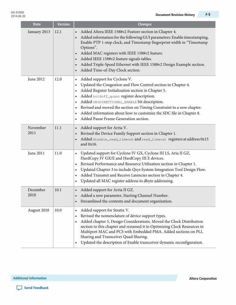
ChangesVersionDate
• Added Altera IEEE 1588v2 Feature section in Chapter 4.• Added information for the followingGUI parameters: Enable timestamping,
Enable PTP 1-step clock, and Timestamp fingerprint width in “TimestampOptions”.
• Added MAC registers with IEEE 1588v2 feature.• Added IEEE 1588v2 feature signals tables.• Added Triple-Speed Ethernet with IEEE 1588v2 Design Example section.• Added Time-of-Day Clock section.
12.1January 2013
• Added support for Cyclone V.• Updated the Congestion and Flow Control section in Chapter 4.• Added Register Initialization section in Chapter 5.• Added holdoff_quant register description.• Added UNIDIRECTIONAL_ENABLE bit description.• Revised and moved the section on Timing Constraint to a new chapter.• Added information about how to customize the SDC file in Chapter 8.• Added Pause Frame Generation section.
12.0June 2012
• Added support for Arria V.• Revised the Device Family Support section in Chapter 1.• Added disable_read_timeout and read_timeout registers at address 0x15
and 0x16.
11.1November2011
• Updated support for Cyclone IV GX, Cyclone III LS, Aria II GZ,HardCopy IV GX/E and HardCopy III E devices.
• Revised Performance and Resource Utilization section in Chapter 1.• Updated Chapter 3 to include Qsys System Integration Tool Design Flow.• Added Transmit and Receive Latencies section in Chapter 4.• Updated all MAC register address to dbyte addressing.
11.0June 2011
• Added support for Arria II GZ.• Added a new parameter, Starting Channel Number.• Streamlined the contents and document organization.
10.1December2010
• Added support for Stratix V.• Revised the nomenclature of device support types.• Added chapter 5, Design Considerations. Moved the Clock Distribution
section to this chapter and renamed it to Optimizing Clock Resources inMultiport MAC and PCS with Embedded PMA. Added sections on PLLSharing and Transceiver Quad Sharing.
• Updated the description of Enable transceiver dynamic reconfiguration.
10.0August 2010
Altera CorporationAdditional Information
Send Feedback
F-5Document Revision HistoryUG-010082014.06.30

ChangesVersionDate
• Added support for Cyclone IV,Hardcopy III, andHardcopy IV, and updatedsupport for Hardcopy II to full.
• Updated chapter 1 to include a feature comparison between 10/100/1000Ethernet MAC and small MAC.
• Updated chapter 4 to revise the 10/100/1000 Ethernet MAC description,Length checking, Reset, and Control Interface sections.
9.1November2009
• Added support for Arria II GX.• Updated chapter 3 to include a new parameter that enables wider statistics
counters.• Updated chapter 4 to reflect support for different speed in multiport MACs
and gated clocks elimination.• Updated chapter 6 to reflect enhancements made on the device drivers.
9.0March 2009
• Updated Chapters 3 and 4 to add description on dynamic reconfiguration.• Updated Chapter 6 to include a procedure to add unsupported PHYs.
8.1November2008
• Revised the performance tables and device support.• Updated Chapters 3 and 4 to include information on MAC with multi ports
and without internal FIFOs.• Revised the clock distribution section in Chapter 4.• Reorganized Chapter 5 to remove redundant information and to include the
new testbench architecture.• Updated Chapter 6 to include new public APIs.
8.0May 2008
• Updated Chapter 1 to reflect new device support.• Updated Chapters 3 and 4 to include information on Small MAC.
7.2October 2007
• Added Chapters 2, 3, 5 and 6.• Updated contents to reflect changes and enhancements in the current version.
7.1May 2007
Updated signal names and description.7.0March 2007
• Global terminology changes: 1000BASE-X PCS/SGMII to 1000BASE-X/SGMII PCS, host side or client side to internal system side,HD to half-duplex.
• Initial release of document on Web.
6.1December2006
Initial release of document on DVD.6.1December2006
Additional InformationAltera Corporation
Send Feedback
UG-01008Document Revision HistoryF-6 2014.06.30

How to Contact Altera
Table F-1: Altera Contact Information
AddressContact MethodContact(3)
www.altera.com/supportWebsiteTechnical support
www.altera.com/trainingWebsiteTechnical training
www.altera.com/literatureWebsiteProduct literature
[email protected] support
[email protected] licensing
Related Information
• www.altera.com/support
• www.altera.com/training
• www.altera.com/literature
(3) You can also contact your local Altera sales office or sales representative.
Altera CorporationAdditional Information
Send Feedback
F-7How to Contact AlteraUG-010082014.06.30