Embed Size (px)
Citation preview
Application Report SLOAxxxx –05/2013
1
TRF7970A External Power Amplifier Kostas Aslanidis, Felix Risch
Embedded RF/ Safety & Security
ABSTRACT
This document is intended to give a practical example on how to design an external power amplifier based on the TRF7970A Transmitter device.
The specific reference design is EMVco compliant in the described configuration.
The design supports ISO14443A, ISO14443B, and ISO15693 as well as the related NFC/RFID protocols/standards.
The design as shown is not intended to be used for long range ISO15693 applications. In such applications the receiver channel has to use improved filters. An optional improved RX filter circuit example is available on the design.
This application note is based on Felix Risch’s Bachelor work of 2013.
SLOAxxxx
2 TRF7970A External Power Amplifier
Contents
1. Scope ............................................................................................................................................... 4 2. Hardware Descriptions: .................................................................................................................. 4 3. TRF7970A Power Amplifier Design ............................................................................................... 5
3.1. Block Diagram ........................................................................................................................... 5 3.2. Schematics ................................................................................................................................ 6 3.3. Board / Layout ........................................................................................................................... 7 3.4. Functional Block Description ..................................................................................................... 8 3.4.1. ................................................................................................................................................. 8 3.4.2. TX/RX Filter ................................................................................................................... 8 3.4.3. Class E Power Amplifier / Adjustment ......................................................................... 10 3.4.4. External Modulation Control ........................................................................................ 11
4. Antenna .......................................................................................................................................... 12 5. TRF7970A EVM Modifications ...................................................................................................... 15 6. Signal Analysis .............................................................................................................................. 16
6.1. Test point definition ................................................................................................................. 16 6.2. Test Point signal overview ....................................................................................................... 17
7. EMVco L1 Test ............................................................................................................................... 22 7.1. TRF7970A Power Amplifier Parameters/Settings ................................................................... 22 7.2. Antenna parameters ................................................................................................................ 22 7.3. EMVco L1 Analog Test Setup ................................................................................................. 23 7.4. Operating Volume Results ...................................................................................................... 23 7.5. Modulation Depth .................................................................................................................... 24 7.6. EMVco L1 Analog Tests .......................................................................................................... 26
8. References ..................................................................................................................................... 31 9. ANNEX ............................................................................................................................................ 32
9.1. Alternative Control Module “MSP-EXP430F5529” .................................................................. 32 9.2. Bill of Material ................................................................................................................................ 34 9.3. Schematic ...................................................................................................................................... 36 10. Revision History ............................................................................................................................ 36
Figures Figure 1: TRF7970A Reference Power Amplifier Circuit 6 Figure 2: TRF7970A Reference Power Amplifier Layout 7 Figure 3: TRF7970A Reference Power Amplifier Board 7 Figure 4: TRF7970A Reference Power Amplifier Functional Module Description 8 Figure 5: RX/TX Circuit 9 Figure 6: RX/TX Filter Characteristic (stand alone |s21|) 9 Figure 7: Class E Amplifier Circuit 10 Figure 8: Class E Circuit Adjustment (Sokal slope) 10 Figure 9: Class E Circuit, Ideal Signal Form at TP2 11 Figure 10: External Modulation Control Circuit 11 Figure 11: Modulation Overshoot Control 12 Figure 12: Reference Antenna (5x5cm) 13 Figure 13: Antenna Smith Chart Matched to 50 Ohm @13.3MHz 13 Figure 14: Magnitude Chart for the Antenna Matched to 50 Ohm @13.3MHz 14 Figure 15: TRF7970A EVM Modifications (Top) 15 Figure 16: TP01 and TP02 Signal overview 17
SLOAxxxx
TRF7970A External Power Amplifier 3
Figure 17: TP02 and TP03 18 Figure 18: TP03 and TP04 19 Figure 19: TP04 and TP05 19 Figure 20: TP05 and TP06 20 Figure 21: Multiplexer TP11 to TP14 20 Figure 22: OPA TP14, TP15 and TP17 21 Figure 23: TRF7970A Reader with Power Amplifier and TRF7970A EVM 22 Figure 24: EMVco Test Setup 23 Figure 25: EMVco Defined Operating Volume 24 Figure 26: 10% Modulation Depth Example 25 Figure 27: EMVco Test PICC, d= 0cm, timing tr/tf 26 Figure 28: EMVco Test PICC, d= 1cm, timing tr/tf 27 Figure 29: EMVco Test PICC, d= 3cm, timing tr/tf 27 Figure 30: EMVco Test PICC, d= 4cm, timing tr/tf 28 Figure 31: EMVco Test PICC Signal, d=0cm 28 Figure 32: EMVco Test PICC Signal, d=2cm 29 Figure 33: EMVco Test PICC Signal, d=4cm 30 Figure 34: MSP-EXP430F5529 board 32 Figure 35: MSP-EXP430F5529 / TRF7970A PA interface 32
Tables Table 1: Voltage at PICC in critical Operating Volume position ................................................................................. 24 Table 2: Modulation Depth Results at 10% Mode ......................................................................................................... 25 Table 3: MSP-EXP430F5529 / TRF7970A PA Interface definition ............................................................................... 33
SLOAxxxx
4 TRF7970A External Power Amplifier
1. Scope
This document is intended to give a practical example on how to design an external power amplifier (PA) based on the TRF7970A NFC/RFID transceiver. The design is primary intended to support the EMVco specifications as well as ISO14443A, ISO14443B, ISO15693, NFC and other standards referring to them. The current implementation is not optimized to give the full reading range performance for the ISO standards given above.
The key feature of this design is the support of the 100% modulation as well as the implementation of the 10% modulation depth from the Reader to Tag communication as used in ISO14443B and ISO15693 and the capability to pass the EMVco L1 Analog specification in the defined configuration.
The current document shows the design of a standalone power amplifier module. At the board an antenna connector for the use of external antennas and Test Points (TP) for fast access to all necessary signals are available.
An interface connector is also available with all necessary signals for the connection to the micro controller board. This external micro controller required to control the TRF7970A and the external amplifier circuit.
An optional RX circuit is included in the circuit concept with optimized filter characteristics for higher sensitivity. Any other concept to further improve the sensitivity can be used.
To simplify the tests procedure, the standard TI TRF7970A EVM with some modifications can be used to control the PA (http://www.ti.com/tool/trf7970aevm).
The FW in the TI TRF7970A EVM to control the PA, is the same used in the standard version on the EVM (www.ti.com/litv/zip/sloc250)
2. Hardware Descriptions:
TRF7970A
Detailed information can be found in http://www.ti.com/product/trf7970a
TRF7970A EVM
Detailed information can be found in http://www.ti.com/tool/trf7970aevm

SLOAxxxx
TRF7970A External Power Amplifier 5
3. TRF7970A Power Amplifier Design
3.1. Block Diagram
TheTRF7970A external Power Amplifier (PA) board contains the TRF7970A IC circuit and the analog modules required for the PA functionality. The PA board is a standalone analog board including the TRF7970A and all the discrete circuitry required as well as an interface connector to the external control board. The concept having no micro controller (uC) on the PA board, keeps the PA design independent from the uC family intended to be used in the application. An external uC module with the control FW has to be connected to the PA board over the interface connector JP1. The communication mode between TRF7970A (on the PA board) and the external uC is SPI with slave select. For the high power generation of the PA, an external power supply is needed to supply the amplifier part with higher voltage. Interface Connector (JP1): The board provides an interface connector (JP1) to be connected to a micro controller (uC) module and the external power supply. The SPI interface is used for the communication between the TRF7970A and the uC. External Antenna: An external antenna has to be connected to the connector (X1). The antenna parameters are defined in chapter 4. TRF7970A Circuit: This part of the PA, implements the basic circuit of the TRF7970A as defined in the datasheet (TRF7970A Data Sheet (SLOS743)). RX/TX Filter: This filter circuit is used for impedance matching between the Class E amplifier output and the antenna impedance. Further the circuit filters the relevant signal components for the communication and eliminate unwanted spurious emission. The RX filter is kept very simple as the read range is sufficient for the EMVco compliance. For improved read range performance an improved circuit is needed in the RX channel. Optional RX Channel: To achieve higher read range, the RX filter characteristics have to be improved. The filter characteristics depend on the requirements, antenna parameters and output power. An example of an improved filter is given in this part of the circuit. Amplifier
SLOAxxxx
6 TRF7970A External Power Amplifier
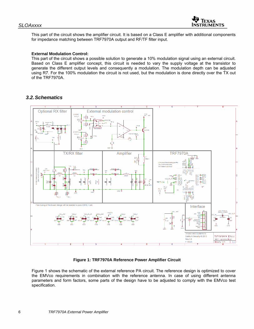
This part of the circuit shows the amplifier circuit. It is based on a Class E amplifier with additional components for impedance matching between TRF7970A output and RF/TF filter input. External Modulation Control: This part of the circuit shows a possible solution to generate a 10% modulation signal using an external circuit. Based on Class E amplifier concept, this circuit is needed to vary the supply voltage at the transistor to generate the different output levels and consequently a modulation. The modulation depth can be adjusted using R7. For the 100% modulation the circuit is not used, but the modulation is done directly over the TX out of the TRF7970A.
3.2. Schematics
Figure 1: TRF7970A Reference Power Amplifier Circuit
Figure 1 shows the schematic of the external reference PA circuit. The reference design is optimized to cover the EMVco requirements in combination with the reference antenna. In case of using different antenna parameters and form factors, some parts of the design have to be adjusted to comply with the EMVco test specification.
SLOAxxxx
TRF7970A External Power Amplifier 7
3.3. Board / Layout
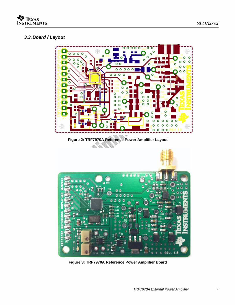
Figure 2: TRF7970A Reference Power Amplifier Layout
Figure 3: TRF7970A Reference Power Amplifier Board

SLOAxxxx
8 TRF7970A External Power Amplifier
3.4. Functional Block Description
TX/RX Filter Amplifier
External Modulation Control
TRF7970ATX_OUT
Figure 4: TRF7970A Reference Power Amplifier Functional Module Description
The basic functional blocks of the design are shown in the module description in Figure 4.
3.4.1.
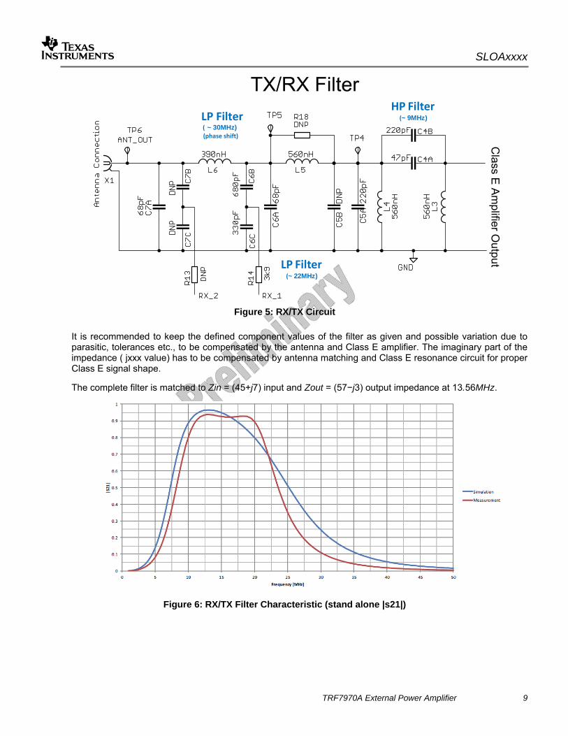
3.4.2. TX/RX Filter The complete filter consists of:
High pass filter with a corner frequency of 8.5MHz Low pass filter with a corner frequency of 21.8MHz and Low pass, filter with a corner frequency of >30MHz. The filter generates a phase shift of about 40-60
deg to prevent read holes. This is required for the RX_2 channel. The TX/RX filter is designed to have an overall band pass characteristic with cut-off frequency about 9MHz – 22MHz.
SLOAxxxx
TRF7970A External Power Amplifier 9
Class E
Am
plifier Output
LP Filter( ~ 30MHz)(phase shift)
LP Filter(~ 22MHz)
HP Filter(~ 9MHz)
Figure 5: RX/TX Circuit
It is recommended to keep the defined component values of the filter as given and possible variation due to parasitic, tolerances etc., to be compensated by the antenna and Class E amplifier. The imaginary part of the impedance ( jxxx value) has to be compensated by antenna matching and Class E resonance circuit for proper Class E signal shape.
The complete filter is matched to Zin = (45+j7) input and Zout = (57−j3) output impedance at 13.56MHz.
Figure 6: RX/TX Filter Characteristic (stand alone |s21|)

SLOAxxxx
10 TRF7970A External Power Amplifier
3.4.3. Class E Power Amplifier / Adjustment
This part of the circuit is supplied by an external power supply with up to 9V1. A class E amplifier generates a RF output power of about 1W (about 20Vpp at TP03). The circuit generates the impedance transformation from 4 Ω (TRF7970A TX out) to 50 Ω (TP03) and signal amplification. The components C1/C2/L2 are used for the matching and resonance frequency of the circuit. The curve shape of the Class E part is very important for the operation in view of efficiency and spurious emissions.
Filt
er In
put
External Modulation Control
Figure 7: Class E Amplifier Circuit
To achieve the best efficiency and signal shape, the circuit can be adjusted according to the guidelines given in Figure 8.
Figure 8: Class E Circuit Adjustment (Sokal slope)
1 External power supply voltage depending on the MOS transistor parameters
SLOAxxxx
TRF7970A External Power Amplifier 11
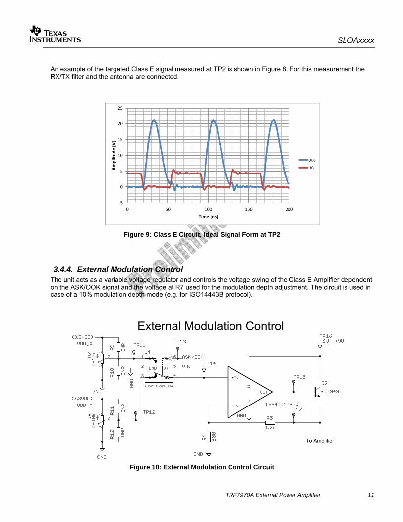
An example of the targeted Class E signal measured at TP2 is shown in Figure 8. For this measurement the RX/TX filter and the antenna are connected.
‐5
0
5
10
15
20
25
0 50 100 150 200
Amplitude [V]
Time [ns]
UDS
UG
Figure 9: Class E Circuit, Ideal Signal Form at TP2
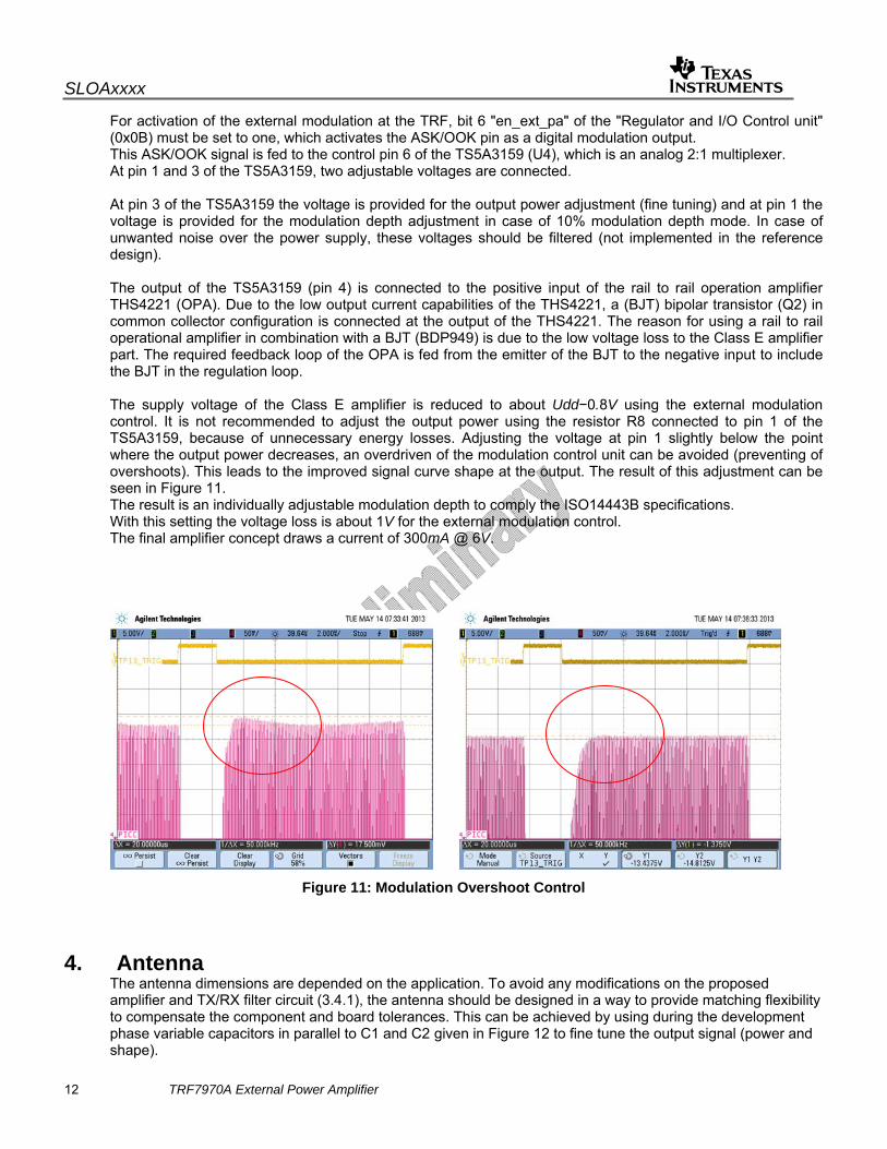
3.4.4. External Modulation Control The unit acts as a variable voltage regulator and controls the voltage swing of the Class E Amplifier dependent on the ASK/OOK signal and the voltage at R7 used for the modulation depth adjustment. The circuit is used in case of a 10% modulation depth mode (e.g. for ISO14443B protocol).
To Amplifier
Figure 10: External Modulation Control Circuit
SLOAxxxx
12 TRF7970A External Power Amplifier
For activation of the external modulation at the TRF, bit 6 "en_ext_pa" of the "Regulator and I/O Control unit" (0x0B) must be set to one, which activates the ASK/OOK pin as a digital modulation output. This ASK/OOK signal is fed to the control pin 6 of the TS5A3159 (U4), which is an analog 2:1 multiplexer. At pin 1 and 3 of the TS5A3159, two adjustable voltages are connected. At pin 3 of the TS5A3159 the voltage is provided for the output power adjustment (fine tuning) and at pin 1 the voltage is provided for the modulation depth adjustment in case of 10% modulation depth mode. In case of unwanted noise over the power supply, these voltages should be filtered (not implemented in the reference design). The output of the TS5A3159 (pin 4) is connected to the positive input of the rail to rail operation amplifier THS4221 (OPA). Due to the low output current capabilities of the THS4221, a (BJT) bipolar transistor (Q2) in common collector configuration is connected at the output of the THS4221. The reason for using a rail to rail operational amplifier in combination with a BJT (BDP949) is due to the low voltage loss to the Class E amplifier part. The required feedback loop of the OPA is fed from the emitter of the BJT to the negative input to include the BJT in the regulation loop. The supply voltage of the Class E amplifier is reduced to about Udd−0.8V using the external modulation control. It is not recommended to adjust the output power using the resistor R8 connected to pin 1 of the TS5A3159, because of unnecessary energy losses. Adjusting the voltage at pin 1 slightly below the point where the output power decreases, an overdriven of the modulation control unit can be avoided (preventing of overshoots). This leads to the improved signal curve shape at the output. The result of this adjustment can be seen in Figure 11. The result is an individually adjustable modulation depth to comply the ISO14443B specifications. With this setting the voltage loss is about 1V for the external modulation control. The final amplifier concept draws a current of 300mA @ 6V.
Figure 11: Modulation Overshoot Control
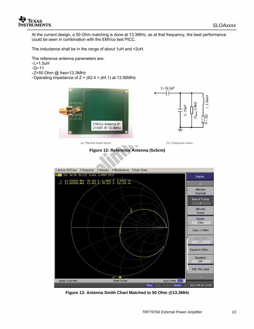
4. Antenna The antenna dimensions are depended on the application. To avoid any modifications on the proposed amplifier and TX/RX filter circuit (3.4.1), the antenna should be designed in a way to provide matching flexibility to compensate the component and board tolerances. This can be achieved by using during the development phase variable capacitors in parallel to C1 and C2 given in Figure 12 to fine tune the output signal (power and shape).
SLOAxxxx
TRF7970A External Power Amplifier 13
At the current design, a 50 Ohm matching is done at 13.3MHz, as at that frequency, the best performance could be seen in combination with the EMVco test PICC. The inductance shall be in the range of about 1uH and <2uH. The reference antenna parameters are: - L=1.5uH - Q~11 - Z=50 Ohm @ fres=13.3MHz - Operating impedance of Z = (62.4 + j44.1) at 13.56MHz
Figure 12: Reference Antenna (5x5cm)
Figure 13: Antenna Smith Chart Matched to 50 Ohm @13.3MHz

SLOAxxxx
14 TRF7970A External Power Amplifier
Figure 14: Magnitude Chart for the Antenna Matched to 50 Ohm @13.3MHz
SLOAxxxx
TRF7970A External Power Amplifier 15
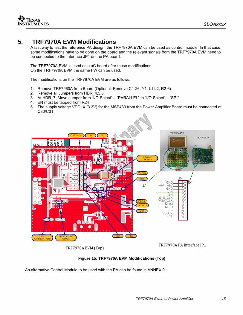
5. TRF7970A EVM Modifications A fast way to test the reference PA design, the TRF7970A EVM can be used as control module. In that case, some modifications have to be done on the board and the relevant signals from the TRF7970A EVM need to be connected to the Interface JP1 on the PA board. The TRF7970A EVM is used as a uC board after these modifications. On the TRF7970A EVM the same FW can be used. The modifications on the TRF7970A EVM are as follows:
1. Remove TRF7960A from Board (Optional: Remove C1-26, Y1, L1,L2, R2-6) 2. Remove all Jumpers from HDR_4,5,6 3. At HDR_7: Move Jumper from “I/O-Select” – “PARALLEL” to “I/O-Select” – “SPI” 4. EN must be tapped from R24 5. The supply voltage VDD_X (3.3V) for the MSP430 from the Power Amplifier Board must be connected at
C30/C31
3)HDR_7“I/O-Select” – “SPI”
5)VDD_X(3.3V)C30/C31
1)Remove TRF7960A
GND
DATA_CLK
Vin(5V)
4)EN
SYS_CLK
MOSI MISO
IRQSS
TRF7970AEVM(Top)TRF7970APAInterfaceJP1
TRF7970AEVM
TRF7970APA2)HDR_4-5-6
Figure 15: TRF7970A EVM Modifications (Top)
An alternative Control Module to be used with the PA can be found in ANNEX 9.1
SLOAxxxx
16 TRF7970A External Power Amplifier
6. Signal Analysis
Several test points (TP) have been included into the design. These TPs simplify the signal observation and adjustments during the development phase. A short explanation of the TPs and the expected signal form is shown below.
6.1. Test point definition TP1 TX-Out signal from TRF7970A TP2 Amplifier signal (UDS) TP3 Class E Amplifier Out TP4 Signal after HP filter TP5 Signal after LP filter TP6 Amplifier OUT, (signal at antenna connector) TP7 RX_1 signal input @ TRF7970 TP8 RX_2 signal input @ TRF7970 TP9 Optional RX channel Input (same as TP5 or TP6 depending on the jumper setting) TP10 Signal after RX channel rectifier TP11 Amplifier power control voltage (fine-tuning for shape adjustment) PA supply voltage TP12 Modulation depth voltage TP13 ASK/OOK Signal from TRF7970A TP14 Multiplexer output voltage TP15 OPA output voltage TP16 Amplifier supply voltage TP17 Output External modulation control circuit.
SLOAxxxx
TRF7970A External Power Amplifier 17
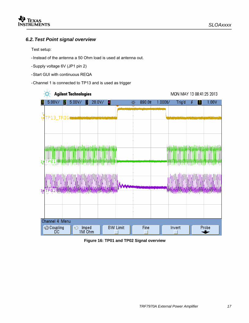
6.2. Test Point signal overview
Test setup:
- Instead of the antenna a 50 Ohm load is used at antenna out.
- Supply voltage 6V (JP1 pin 2)
- Start GUI with continuous REQA
- Channel 1 is connected to TP13 and is used as trigger
Figure 16: TP01 and TP02 Signal overview
SLOAxxxx
18 TRF7970A External Power Amplifier
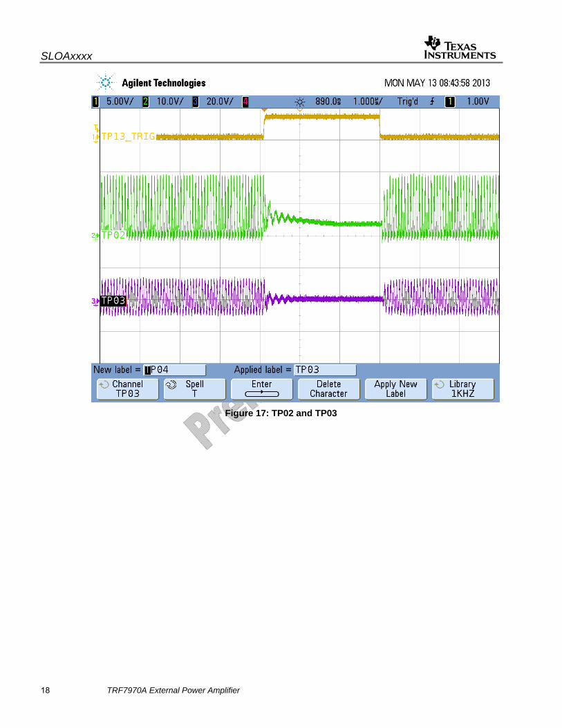
Figure 17: TP02 and TP03

SLOAxxxx
TRF7970A External Power Amplifier 19
Figure 18: TP03 and TP04
Figure 19: TP04 and TP05
SLOAxxxx
20 TRF7970A External Power Amplifier
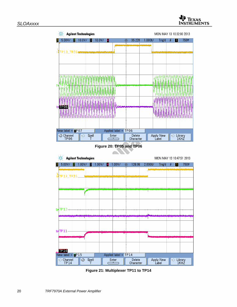
Figure 20: TP05 and TP06
Figure 21: Multiplexer TP11 to TP14
SLOAxxxx
TRF7970A External Power Amplifier 21
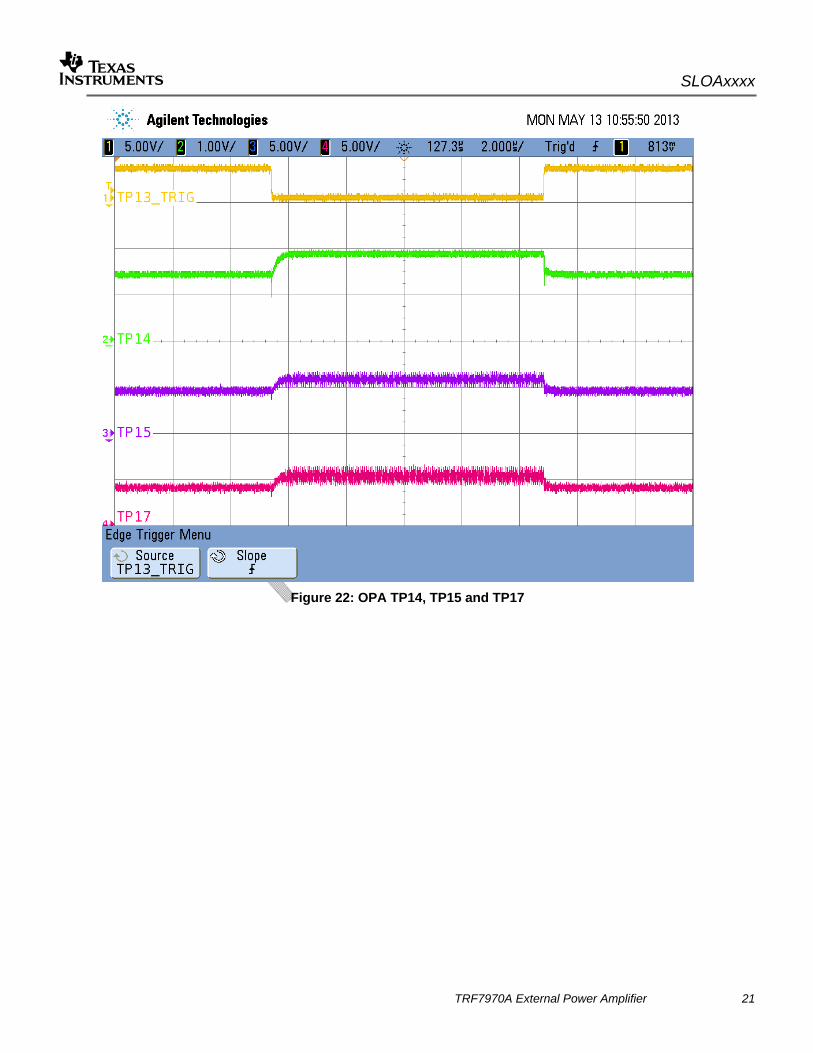
Figure 22: OPA TP14, TP15 and TP17
SLOAxxxx
22 TRF7970A External Power Amplifier
7. EMVco L1 Test
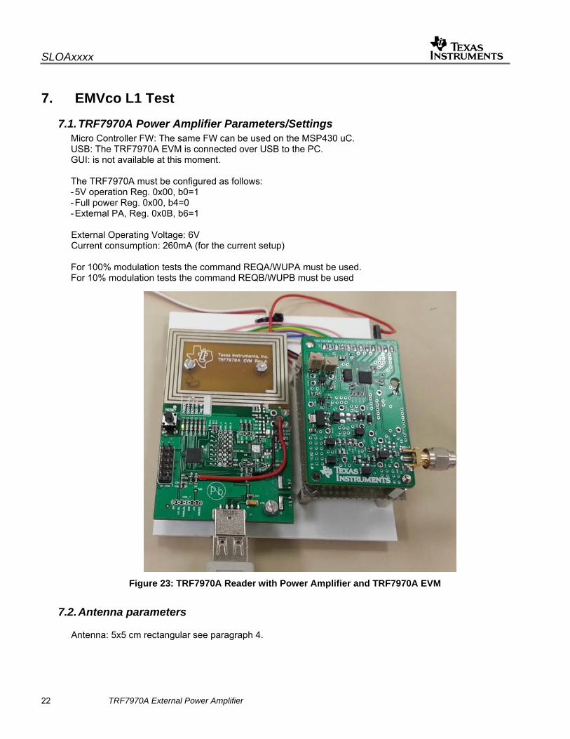
7.1. TRF7970A Power Amplifier Parameters/Settings Micro Controller FW: The same FW can be used on the MSP430 uC. USB: The TRF7970A EVM is connected over USB to the PC. GUI: is not available at this moment. The TRF7970A must be configured as follows: - 5V operation Reg. 0x00, b0=1 - Full power Reg. 0x00, b4=0 - External PA, Reg. 0x0B, b6=1
External Operating Voltage: 6V Current consumption: 260mA (for the current setup)
For 100% modulation tests the command REQA/WUPA must be used. For 10% modulation tests the command REQB/WUPB must be used
Figure 23: TRF7970A Reader with Power Amplifier and TRF7970A EVM
7.2. Antenna parameters
Antenna: 5x5 cm rectangular see paragraph 4.
SLOAxxxx
TRF7970A External Power Amplifier 23
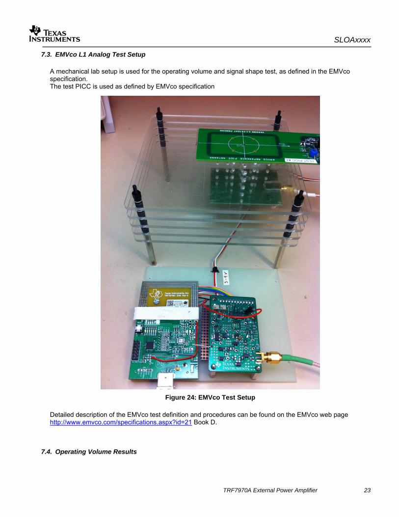
7.3. EMVco L1 Analog Test Setup
A mechanical lab setup is used for the operating volume and signal shape test, as defined in the EMVco specification. The test PICC is used as defined by EMVco specification
Figure 24: EMVco Test Setup
Detailed description of the EMVco test definition and procedures can be found on the EMVco web page http://www.emvco.com/specifications.aspx?id=21 Book D.
7.4. Operating Volume Results
SLOAxxxx
24 TRF7970A External Power Amplifier
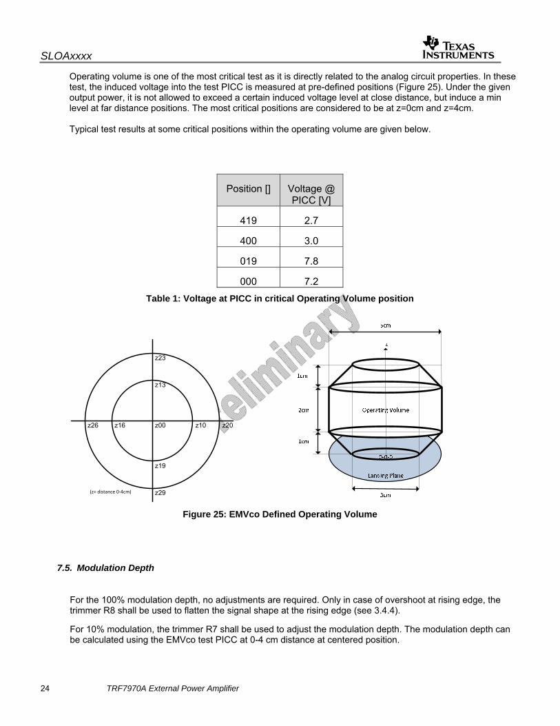
Operating volume is one of the most critical test as it is directly related to the analog circuit properties. In these test, the induced voltage into the test PICC is measured at pre-defined positions (Figure 25). Under the given output power, it is not allowed to exceed a certain induced voltage level at close distance, but induce a min level at far distance positions. The most critical positions are considered to be at z=0cm and z=4cm. Typical test results at some critical positions within the operating volume are given below.
Position [] Voltage @ PICC [V]
419 2.7
400 3.0
019 7.8
000 7.2
Table 1: Voltage at PICC in critical Operating Volume position
z00 z10 z20
z13
z23
z16z26
z19
z29(z= distance 0‐4cm)
Figure 25: EMVco Defined Operating Volume
7.5. Modulation Depth
For the 100% modulation depth, no adjustments are required. Only in case of overshoot at rising edge, the trimmer R8 shall be used to flatten the signal shape at the rising edge (see 3.4.4).
For 10% modulation, the trimmer R7 shall be used to adjust the modulation depth. The modulation depth can be calculated using the EMVco test PICC at 0-4 cm distance at centered position.

SLOAxxxx
TRF7970A External Power Amplifier 25
The resulting values are recommended to be within 10-14% modulation depth. Detailed modulation depth limits at the different positions can be found in the EMVco specification http://www.emvco.com/specifications.aspx?id=21 Book D.
Typical modulation depth results of the current design:
Distance [cm]
Mod. Depth [%]
0 13.1
1 13.3
2 13.3
3 12.6
4 12.8
Table 2: Modulation Depth Results at 10% Mode
To avoid generation of inverse modulation during the 10% adjustment, Figure 26 shows the RF pattern of the WUPB command.
Figure 26: 10% Modulation Depth Example
SLOAxxxx
26 TRF7970A External Power Amplifier
7.6. EMVco L1 Analog Tests
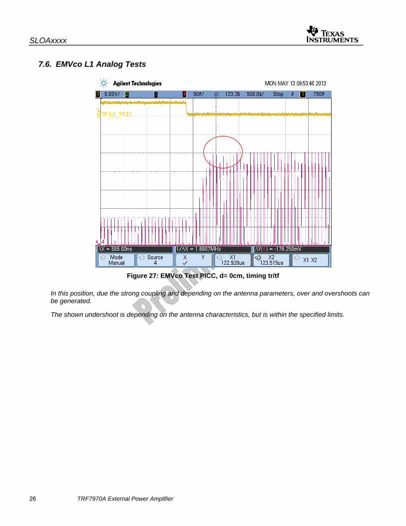
Figure 27: EMVco Test PICC, d= 0cm, timing tr/tf
In this position, due the strong coupling and depending on the antenna parameters, over and overshoots can be generated.
The shown undershoot is depending on the antenna characteristics, but is within the specified limits.
SLOAxxxx
TRF7970A External Power Amplifier 27
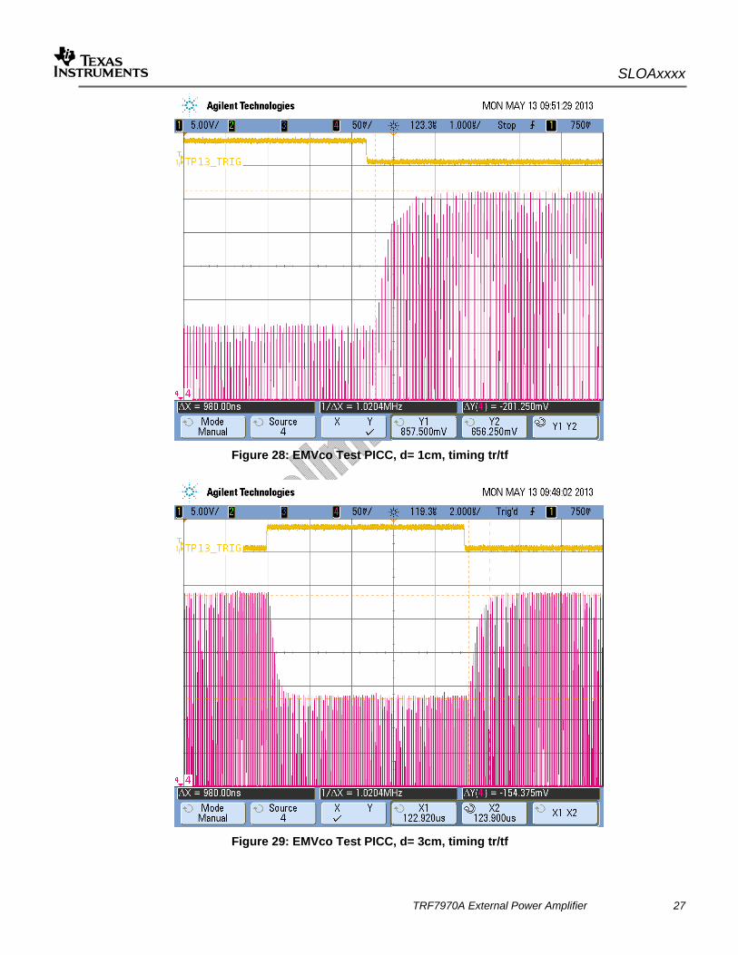
Figure 28: EMVco Test PICC, d= 1cm, timing tr/tf
Figure 29: EMVco Test PICC, d= 3cm, timing tr/tf

SLOAxxxx
28 TRF7970A External Power Amplifier
Figure 30: EMVco Test PICC, d= 4cm, timing tr/tf
Figure 31: EMVco Test PICC Signal, d=0cm
In this position, due the strong coupling and depending on the antenna parameters, over and overshoots can be generated. The shown overshoot is depending on the antenna characteristics, but is within the specified limits.
SLOAxxxx
TRF7970A External Power Amplifier 29
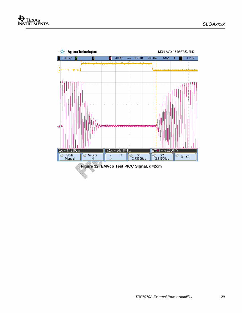
Figure 32: EMVco Test PICC Signal, d=2cm
SLOAxxxx
30 TRF7970A External Power Amplifier
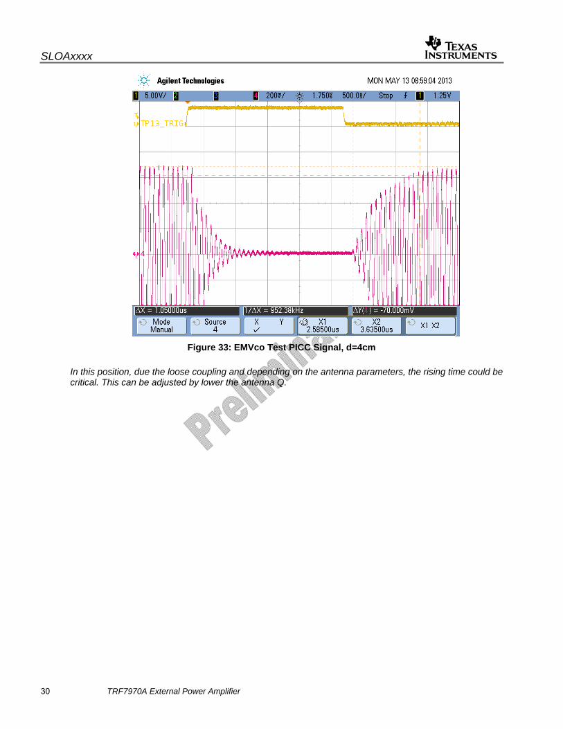
Figure 33: EMVco Test PICC Signal, d=4cm
In this position, due the loose coupling and depending on the antenna parameters, the rising time could be critical. This can be adjusted by lower the antenna Q.

SLOAxxxx
TRF7970A External Power Amplifier 31
8. References 1. Texas Instruments http://www.ti.com/
2. TI Wireless Connectivity / RFID / NFC
3. TRF7970A Data Sheet (SLOS743)
4. TRF7970A EVM (http://www.ti.com/tool/trf7970aevm )
5. ISO/IEC14443-2:2009(E)
6. ISO/IEC14443-3:2009(E)
7. ISO/IEC14443-4:2008(E)
8. EMVco (http://www.emvco.com/ )
9. Sokal slope (http://www.eel.ufsc.br/~lci/siteramo/documentos/mestres/artigos/classe.pdf )

SLOAxxxx
32 TRF7970A External Power Amplifier
9. ANNEX
9.1. Alternative Control Module “MSP-EXP430F5529”
An alternative control module which can be used with the TRF7970A Power Amplifier board is the MSP-EXP430F5529 (http://www.ti.com/tool/msp-exp430f5529). This HW can be used in combination with the TI NFCLink FW for the board.
Figure 34: MSP-EXP430F5529 board
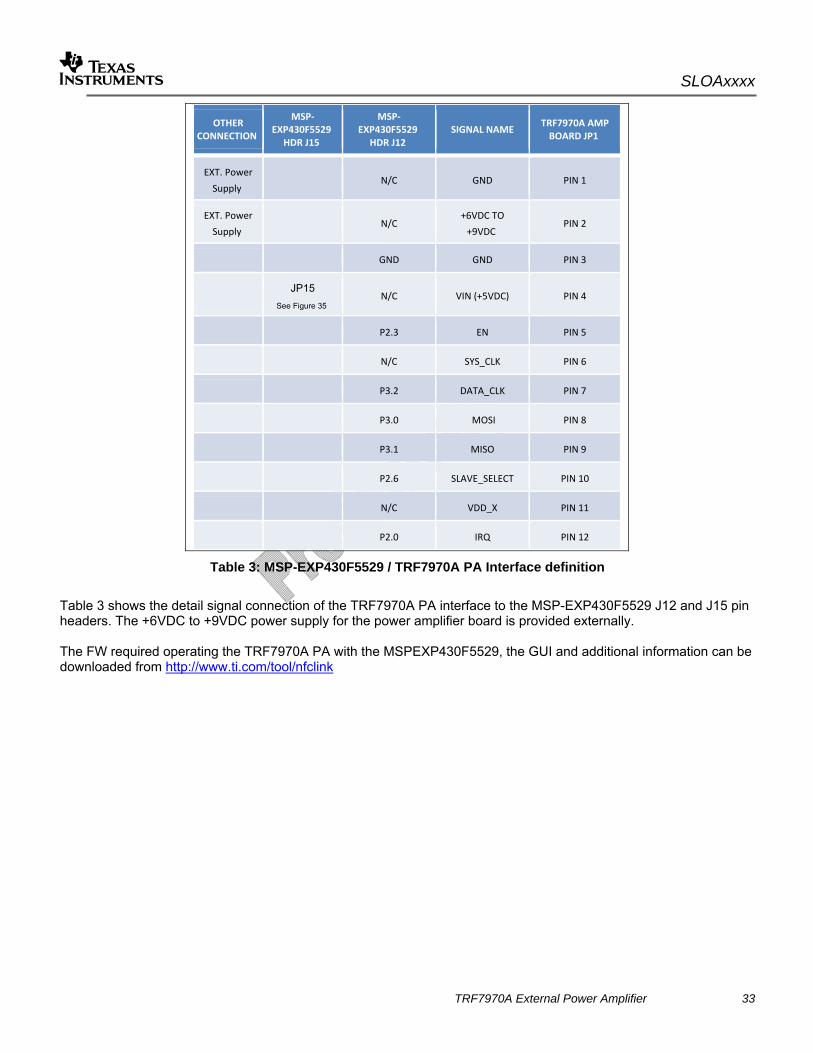
For operation the TRF7970A Power Amplifier board has to be connected to the MSP-EXP430F5529 board. J12 marked in Figure 34 is used to interface with the TRF7970A Power Amplifier board (JP1). The detailed connection guidance can be found below.
Figure 35: MSP-EXP430F5529 / TRF7970A PA interface
SLOAxxxx
TRF7970A External Power Amplifier 33
OTHER CONNECTION
MSP‐EXP430F5529
HDR J15 MSP‐
EXP430F5529 HDR J12
SIGNAL NAME TRF7970A AMP BOARD JP1
EXT. Power
Supply N/C GND PIN 1
EXT. Power
Supply N/C +6VDC TO
+9VDC PIN 2
GND GND PIN 3
JP15
See Figure 35 N/C VIN (+5VDC) PIN 4
P2.3 EN PIN 5 N/C SYS_CLK PIN 6 P3.2 DATA_CLK PIN 7 P3.0 MOSI PIN 8 P3.1 MISO PIN 9 P2.6 SLAVE_SELECT PIN 10 N/C VDD_X PIN 11 P2.0 IRQ PIN 12
Table 3: MSP-EXP430F5529 / TRF7970A PA Interface definition
Table 3 shows the detail signal connection of the TRF7970A PA interface to the MSP-EXP430F5529 J12 and J15 pin headers. The +6VDC to +9VDC power supply for the power amplifier board is provided externally. The FW required operating the TRF7970A PA with the MSPEXP430F5529, the GUI and additional information can be downloaded from http://www.ti.com/tool/nfclink
SLOAxxxx
34 TRF7970A External Power Amplifier
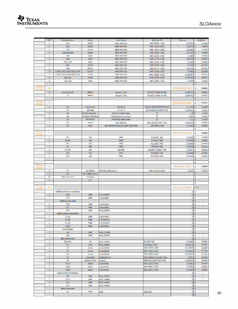
9.2. Bill of Material
The BOM will be available on the TI TRF7970A EVM Product Folder http://www.ti.com/tool/trf7970aevm
BOM
SLOAxxxx
TRF7970A External Power Amplifier 35
SLOAxxxx
36 TRF7970A External Power Amplifier
9.3. Schematic
The Schematic and Board layout files in Eagle format and Gerber files, will be available on the TI TRF7970A EVM Product Folder http://www.ti.com/tool/trf7970aevm
10. Revision History
Revision Data Changes Comment
28-05-2013 Initial release
V53 21-05-2013 Added 9.1