Embed Size (px)
Citation preview

Technion 046188/2012 Lect 06
Lecture 06
DIGITAL TO ANALOG CONVERTERS
Welcome to046188 Winter semester 2012Mixed Signal Electronic Circuits
Instructor: Dr. M. Moyal
Transfer FunctionDAC architectures/Examples Calibrations
www.gigalogchip.com

Technion 046188/2012 Lect 06
Transfer FunctionDAC architecturesDAC Example Calibrations
Agenda

Technion 046188/2012 Lect 06
Equation (Binary weighted DAC)
ExampleA 4 bit DAC having n=4 bits will have 4 digital inputs from 0000 to 1111. (0-15)
Vout (Fscale) = Vref(1/16) x [ B0 x1 + B1 x (2) + B2 x (4) + B3 x (8)]. = 15/16 x Vref
Can also be called “multiplying dac”B’s is a digital code, it is assumed a 0 value or a 1 value ( digital codes)
Vref is a reference set by design to control the output range (supply range is the limitation, ~Vdd-0.6)
The minimum step is assume when B0=1 all other B’s are 0! Is the Least significant bit (LSB).
Transfer Function
DAC Basics: D/A conversion does not change the Spe ctrum of the input signal
Technion 046188/2012 Lect 06
Transfer Function (TF)
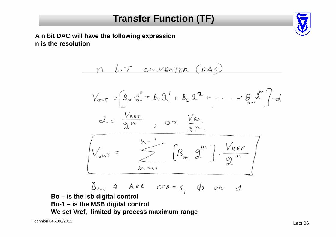
A n bit DAC will have the following expressionn is the resolution
Bo – is the lsb digital controlBn-1 – is the MSB digital controlWe set Vref, limited by process maximum range
Technion 046188/2012 Lect 06
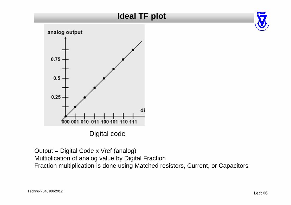
Output = Digital Code x Vref (analog) Multiplication of analog value by Digital Fraction Fraction multiplication is done using Matched resistors, Current, or Capacitors
Digital code
Ideal TF plot

Technion 046188/2012 Lect 06
Misc..Frequency domain in sampling
Technion 046188/2012 Lect 06
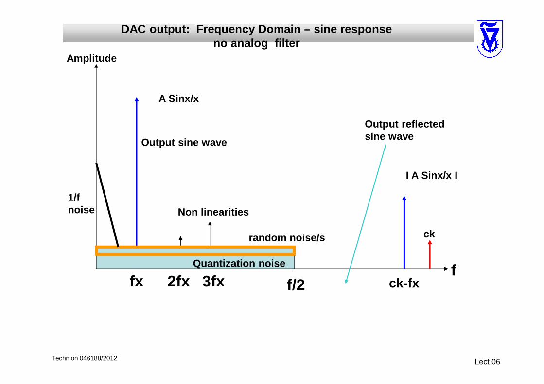
DAC output: Frequency Domain – sine responseno analog filter
f f/2
ck
Output sine wave
Output reflected sine wave
fx ck-fx 2fx 3fx Quantization noise
random noise/s
Amplitude
I A Sinx/x I
A Sinx/x
1/fnoise Non linearities

Technion 046188/2012 Lect 06
ISinx/xI means what !Example:
If fin lies at ¼ fs ! ( fs=1MHz and fin=250KHz )
Pi x ¾ = 135 deg.
Sin(135) / 3.14x3/4 = 0.707/2.355=0.3
Technion 046188/2012 Lect 06
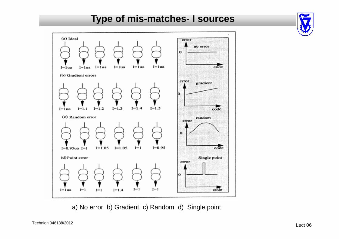
a) No error b) Gradient c) Random d) Single point
Type of mis-matches- I sources

Technion 046188/2012 Lect 06
1 2 3 45 6 7 89 10 11 12
13 14 15 16
1 2 3 4 5 6 7 8 9 10 11 12 13 14 15 16
10 12 9 112 4 1 3
14 16 13 156 8 5 7
gradient
gradient
gradient
gradient
gradient
Common centered design
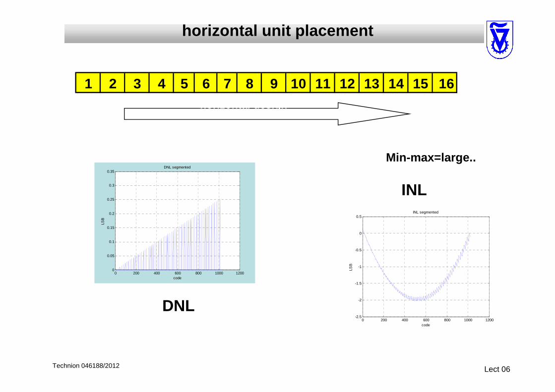
horizontal design
Thermometer unit placement architecture: Gradient affect
Shufle designHorizontal/Vertical
Horizontal
Technion 046188/2012 Lect 06
1 2 3 4 5 6 7 8 9 10 11 12 13 14 15 16
gradienthorizontal design
0 200 400 600 800 1000 12000
0.05
0.1
0.15
0.2
0.25
0.3
0.35DNL segmented
code
LSB
0 200 400 600 800 1000 1200-2.5
-2
-1.5
-1
-0.5
0
0.5INL segmented
code
LSB
DNL
INL
horizontal unit placement
Min-max=large..

Technion 046188/2012 Lect 06
1 2 3 45 6 7 89 10 11 12
13 14 15 16
gradient
gradient
0 200 400 600 800 1000 12000
0.01
0.02
0.03
0.04
0.05
0.06
0.07DNL segmented
code
LSB
INL
0 200 400 600 800 1000 1200-0.3
-0.25
-0.2
-0.15
-0.1
-0.05
0
0.05INL segmented
code
LSB
DNL
Min-max=~0.27lsb
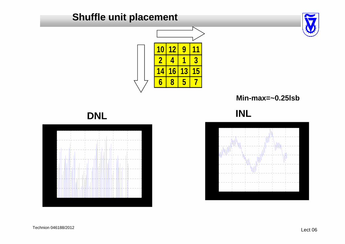
Horizontal/Vertical unit placement
Technion 046188/2012 Lect 06
10 12 9 112 4 1 3
14 16 13 156 8 5 7
gradient
gradient
Shuffle unit placement
0 200 400 600 800 1000 12000
0.01
0.02
0.03
0.04
0.05
0.06
0.07DNL segmented
code
LSB
DNL
0 200 400 600 800 1000 1200-0.2
-0.15
-0.1
-0.05
0
0.05
0.1
0.15INL segmented
code
LSB
INL
Min-max=~0.25lsb
Technion 046188/2012 Lect 06
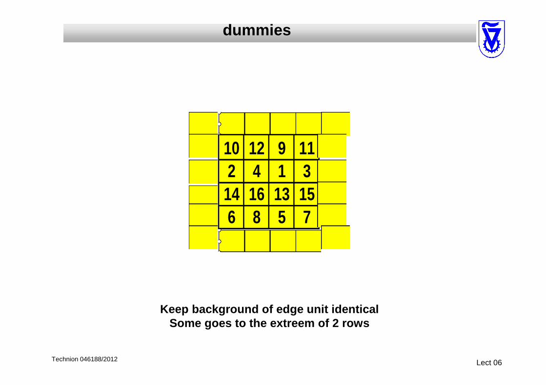
10 12 9 112 4 1 3
14 16 13 156 8 5 7
dummies
Keep background of edge unit identicalSome goes to the extreem of 2 rows
Technion 046188/2012 Lect 06
DACs Architectures
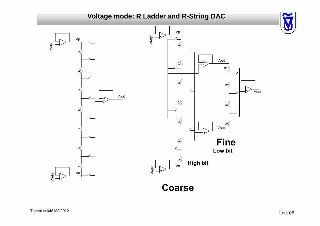
Voltage mode: R Ladder and R-String DACThe Basic R-2R DACR and I DACC DACCurrent (steering) DAC
Technion 046188/2012 Lect 06
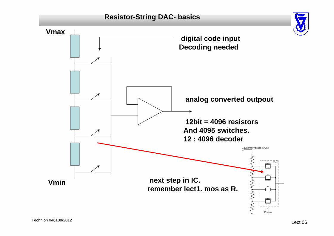
Resistor-String DAC- basics
12bit = 4096 resistors And 4095 switches.12 : 4096 decoder
Vmax
Vmin
digital code inputDecoding needed
analog converted outpout
next step in IC.remember lect1. mos as R.
Technion 046188/2012 Lect 06
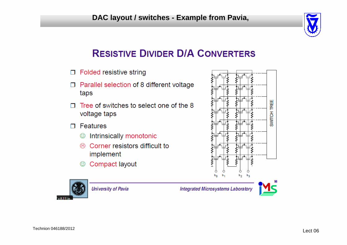
DAC layout / switches - Example from Pavia,

Technion 046188/2012 Lect 06
DAC different IDEA. – 2 nd Example from Pavia,
Technion 046188/2012 Lect 06
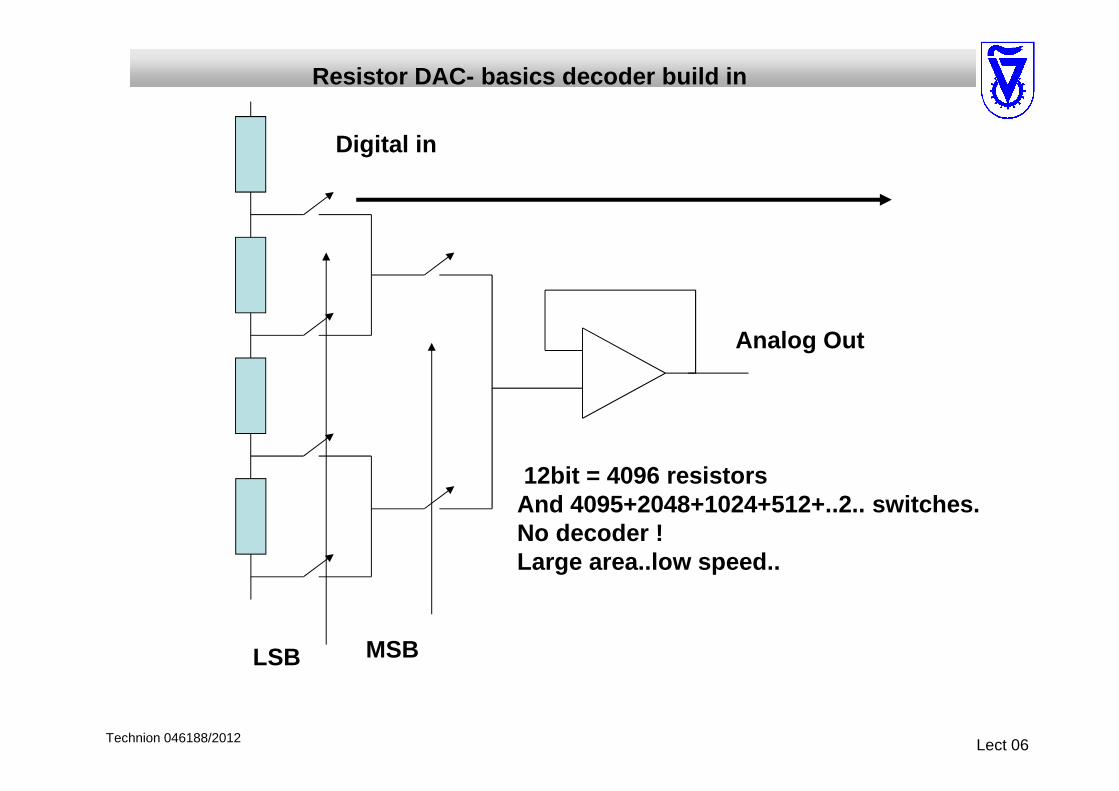
12bit = 4096 resistors And 4095+2048+1024+512+..2.. switches.No decoder !Large area..low speed..
Digital in
Analog Out
LSB MSB
Resistor DAC- basics decoder build in

Technion 046188/2012 Lect 06
Technion 046188/2012 Lect 06
Voltage mode: R Ladder and R-String DAC
Vout
RR
RR
RR
R
Vre
fnV
refp
Vp
Vn
Vout
RR
RR
RR
R
Vre
fnV
refp
Vp
Vn
Vout
RR
RR
Vout
Coarse
FineLow bit
High bit
Technion 046188/2012 Lect 06
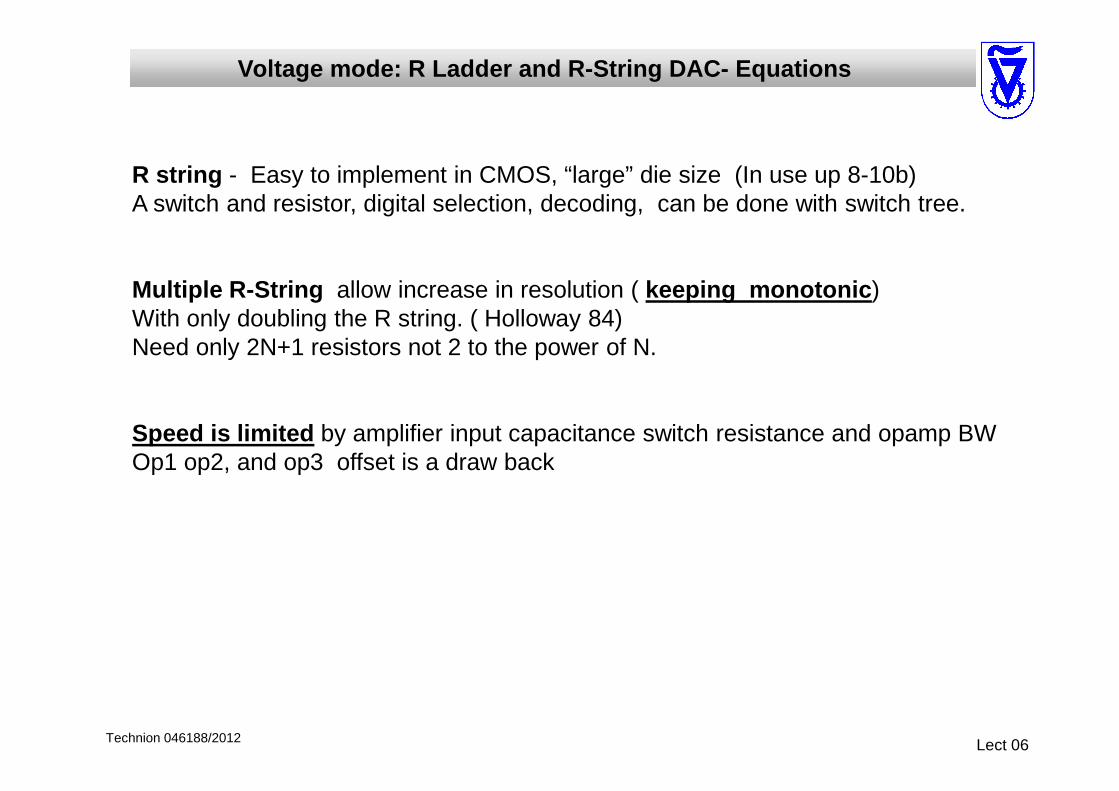
R string - Easy to implement in CMOS, “large” die size (In use up 8-10b)A switch and resistor, digital selection, decoding, can be done with switch tree.
Multiple R-String allow increase in resolution ( keeping monotonic ) With only doubling the R string. ( Holloway 84) Need only 2N+1 resistors not 2 to the power of N.
Speed is limited by amplifier input capacitance switch resistance and opamp BWOp1 op2, and op3 offset is a draw back
Voltage mode: R Ladder and R-String DAC- Equations

Technion 046188/2012 Lect 06
THE BASIC R-2R DAC
Motivation: lower area, 12b=25 resistors
No guaranteed monotonic, bad offset sensitivity

Technion 046188/2012 Lect 06
Vmid
Vout
R R R R R RVref
a6 a5 a4 a3 a0a1
R
Operation- unipolar output:
msb I(a6=H)= -Vref/2R only a6 goes HI(a5=H)= -Vref/4R
lsb I(a0=H)= -Vref/128R only a0=HI total = -Vref/R – Vref/128R all switches to out=H
Bipolar output possible with an extra amplifier and the use of Vmid

Technion 046188/2012 Lect 06
R-2R key issues
Very common architecture if thin film resistors are used ( Cecil 74)Area efficient- Easy to increase resolution R-2R per bit Monotonic is not granted INL and DNL are closely coupledRelatively Slow
“rule of thumb” : Matching requirement for the n th bit in the i th bit

Technion 046188/2012 Lect 06
can we Fix the impedance issue
w/l
w/2l
Match the switches
2) Problem: Output impedance changes and get multip lied by amplifier offsetLooking from the other side (opamp side) R looking back form the amplifier vary with code.
1) Switch resistance, Vgs voltage changes will effect mismatches
RR
R

Technion 046188/2012 Lect 06
R-2R and I
Source: R V Plasshe
Technion 046188/2012 Lect 06
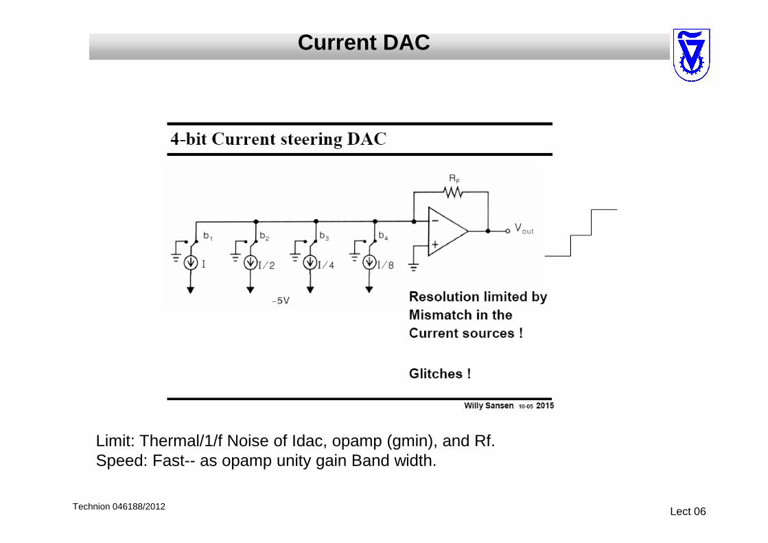
Current DAC
Limit: Thermal/1/f Noise of Idac, opamp (gmin), and Rf. Speed: Fast-- as opamp unity gain Band width.

Technion 046188/2012 Lect 06
I dac with reference

Technion 046188/2012 Lect 06
Glitch control Coding schemes..:
Good around +/-0

Technion 046188/2012 Lect 06

Technion 046188/2012 Lect 06
DAC with ..- sign magnitude..
Technion 046188/2012 Lect 06

Technion 046188/2012 Lect 06
Technion 046188/2012 Lect 06
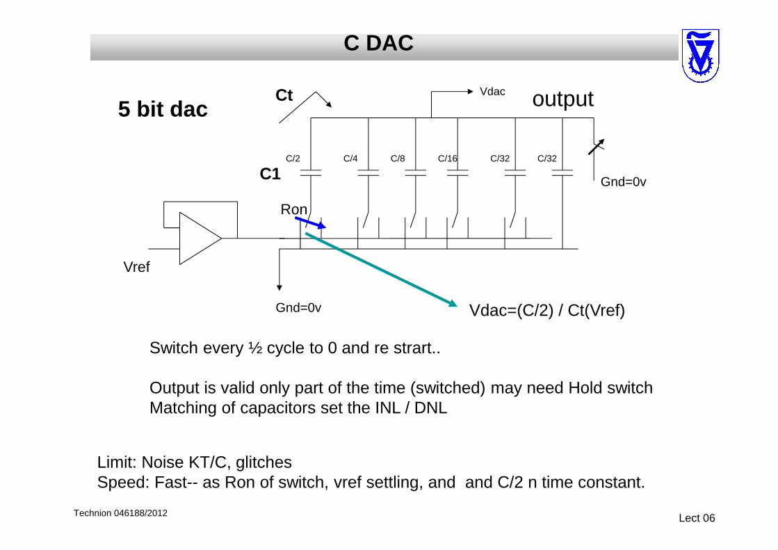
C DAC
Switch every ½ cycle to 0 and re strart..
Output is valid only part of the time (switched) may need Hold switchMatching of capacitors set the INL / DNL
Vref
Gnd=0v
Vdac
C/2 C/4 C/8 C/16 C/32 C/32
5 bit dac
Gnd=0v
Limit: Noise KT/C, glitches Speed: Fast-- as Ron of switch, vref settling, and and C/2 n time constant.
Ron
Vdac=(C/2) / Ct(Vref)
C1
Ct output

Technion 046188/2012 Lect 06
I dac - binary
Source: B. Murmann Stanford
I dac - thermometer
Could be non Monotonic- in transitionsSimple decoder
Monotonic- guaranteed
decoder complex001 000000001010 000000011011 000000111 always one change100 000001111“best” for speed => Iout time
constant

Technion 046188/2012 Lect 06
Binary Vs. Thermometer - mismatch
Source : JSCC IEEE 1998 Chi-Hung 10b 500Mhz
Matlab 1000 simulationsFOR THE SAME AREA INL – THE SAME DNL – BIG DIFFERENEFigure out the optimum place: how many binary bits and how many segmented bit

Technion 046188/2012 Lect 06
DAC Response
Partly Source: WilleSansen 2007
Inaccuracy/offset
Capacitive charge

Technion 046188/2012 Lect 06
Glitches and INL in Binary dac
If the glitches scale with code (and capacitance is linear) – Linearity is good
Technion 046188/2012 Lect 06
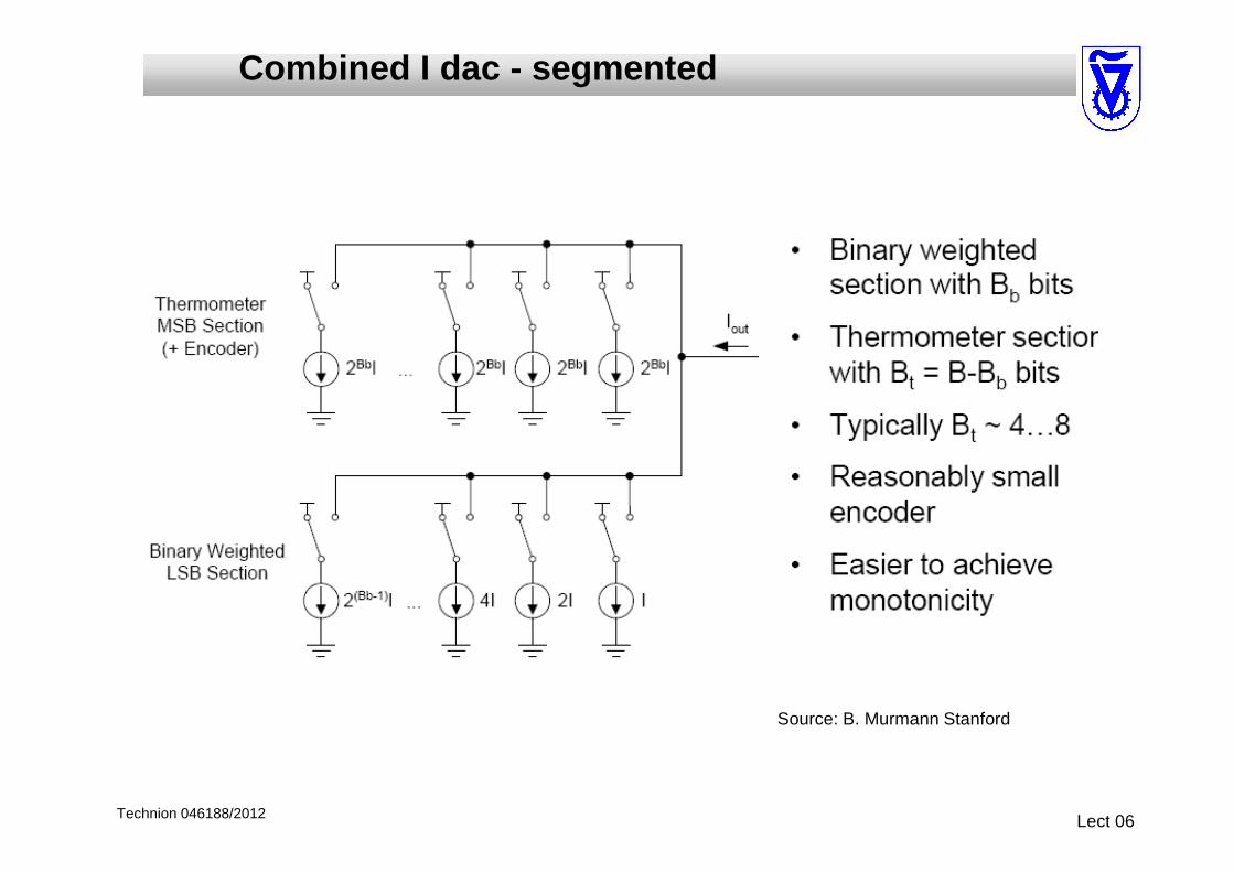
Combined I dac - segmented
Source: B. Murmann Stanford

Technion 046188/2012 Lect 06
Current (steering) DAC - removed opamp
Source : G. Gielen, K.U.L Leuven
Technion 046188/2012 Lect 06
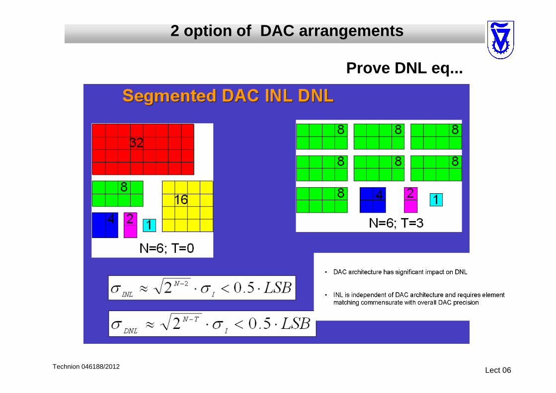
2 option of DAC arrangements
Prove DNL eq...

Technion 046188/2012 Lect 06
Technion 046188/2012 Lect 06
Drain
Source
Gate
Drain
Source
Drain
Dummy
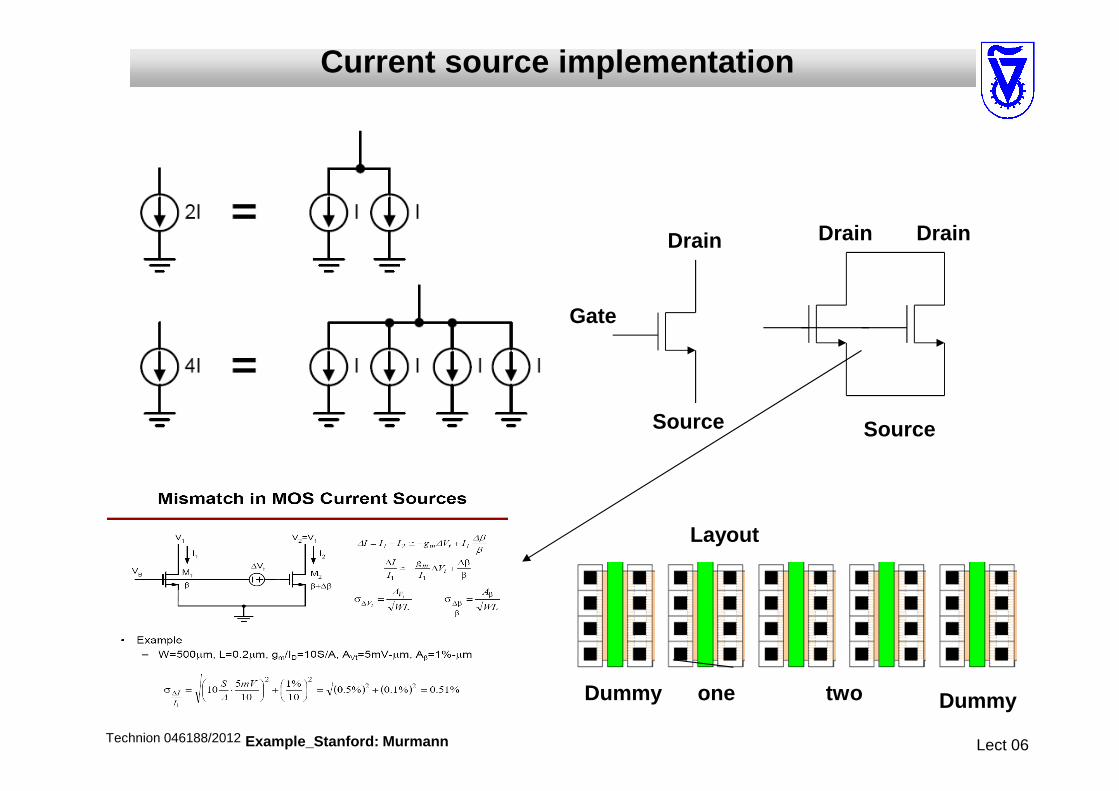
Current source implementation
one two Dummy
Layout
Example_Stanford: Murmann

Technion 046188/2012 Lect 06
Binary Weighted
Differential I/2I mode DAC TYPES
Very FastCompact N latches ( but need to be sized up)Linearity limited by MSB DNL spikes: in some code transitions
Use twice the current on the bottomBut only N channel switches (CML

Technion 046188/2012 Lect 06
Voutn
I
vb2
latch
anck
I
latch
I
latch
I
latch
a1
a0
r1
Vout
r2 Vmid
Vdd
N units
N I
0.5N I 0.5N I
Current source matching relaxed (DNL) Each stage is LSB equivalent in contributionFor N bit, 2 to power of N latches, unit cells, wires Silicon area is large, depend on marching and routingPower supply grounding is important I deal: Can combine with Binary approach and leave some MSB as Segmented
Thermometer

Technion 046188/2012 Lect 06
Voutn
vb 8I
7.5Ivb2
latch
a3ck
4I
latch
2I
latch
I
latch
a2 a1 a0
lsbmsb
r1
Vout
r2 Vmid
Vdd
7.5I
Fix the output impedance variationsAnd add the « out of ban » noise reduction filter
Virtual mid voltageNon moving
Slow now
DAC with reduced Rout effect and filter
Filter
From DAC LineDriver
Power back-off
++
- -+
- -
+

Technion 046188/2012 Lect 06
Pre driver
Technion 046188/2012 Lect 06
Iout
DAC
Ioutn
Vpb
Vnb
Control
Vdd
Bit1
8bit thermometer
Vss
6bit binary
Filter
From DAC LineDriver
Power back-off
++
- -+
- -
+
OUTN
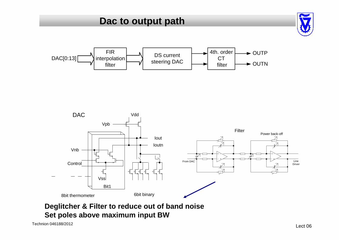
OUTPDAC[0:13] DS current
steering DAC
4th. orderCT
filter
FIRinterpolation
filter
Dac to output path
Deglitcher & Filter to reduce out of band noiseSet poles above maximum input BW

Technion 046188/2012 Lect 06
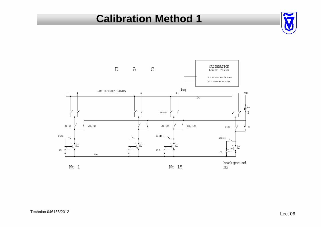
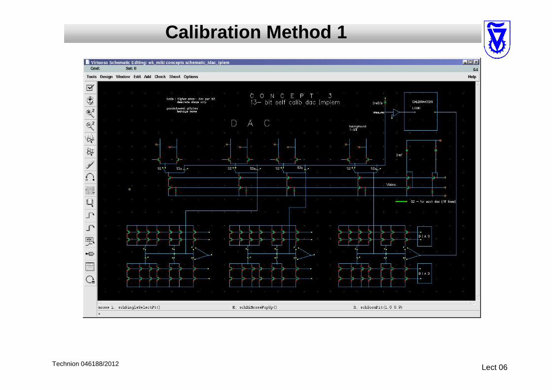
Calibration Methods
1) Make all I the same2) Add error I3) Dynamic Averaging
Technion 046188/2012 Lect 06
Calibration Method 1
Technion 046188/2012 Lect 06
Calibration Method 1

Technion 046188/2012 Lect 06
End lecture 06
www.gigalogchip.com