Embed Size (px)
Citation preview

VIN
PGND
VIN
VOUT
RFBB
VOUT
FB
RFBT
CIN
COUT
PGOOD
EN
RT/CLK
RRTTPSM84424
Copyright © 2018, Texas Instruments Incorporated
AGND
TT
RTT
Product
Folder
Order
Now
Technical
Documents
Tools &
Software
Support &Community
An IMPORTANT NOTICE at the end of this data sheet addresses availability, warranty, changes, use in safety-critical applications,intellectual property matters and other important disclaimers. PRODUCTION DATA.
TPSM84424SLVSEJ2A –FEBRUARY 2018–REVISED APRIL 2018
TPSM84424 4.5-V to 17-V Input, 0.6-V to 10-V Output, 4-A Power Module
1
1 Features1• Integrated Inductor Power Solution• 7.5 mm × 7.5 mm × 5.3 mm QFM Package
– All Pins Accessible from Package Perimeter• Input Voltage Range: 4.5 V to 17 V• Wide-Output Voltage Range: 0.6 V to 10 V• Efficiencies up to 96%• Adjustable Fixed Switching Frequency
(200 kHz to 1.6 MHz)• Allows Synchronization to an External Clock• Ultra-Fast Load Step Response (TurboTrans™)• Power Good Output• Meets EN55011 Class B Radiated EMI Limits• Operating Ambient Range: –40°C to +105°C• Operating IC Junction Range: –40°C to +150°C• Create a Custom Design Using the TPSM84424
With the WEBENCH® Power Designer
2 Applications• Telecom and Wireless Infrastructure• Industrial Automated Test Equipment• Enterprise Switching and Storage Applications• High Density Distributed Power Systems
spacespace
3 DescriptionThe TPSM84424 power module is an easy-to-useintegrated power supply that combines a 4-A DC/DCconverter with power MOSFETs, a shielded inductorand passives into a small form factor, QFM package.This power solution allows as few as six externalcomponents while maintaining the ability to adjust keyparameters to meet specific design requirements.Ultra-fast transient response can be achieved by useof the TurboTrans™ feature. TurboTrans allows thetransient response to be optimized for reduced outputvoltage deviation with less required outputcapacitance.
The 7.5 mm × 7.5 mm × 5.3 mm, 24-pin, QFMpackage is easy to solder to a printed circuit boardand has excellent power dissipation capability. TheTPSM84424 offers flexibility with many featuresincluding power good, programmable UVLO, tracking,prebias start-up, as well as overcurrent andovertemperature protection making it ideal forpowering a wide range of devices and systems.
Device Information(1)
PART NUMBER PACKAGE BODY SIZE (NOM)TPSM84424 QFM (24) 7.50 mm × 7.50 mm
(1) For all available packages, see the orderable addendum atthe end of the data sheet.
space
spaceSimplified Schematic
Transient Response

2
TPSM84424SLVSEJ2A –FEBRUARY 2018–REVISED APRIL 2018 www.ti.com
Product Folder Links: TPSM84424
Submit Documentation Feedback Copyright © 2018, Texas Instruments Incorporated
Table of Contents1 Features .................................................................. 12 Applications ........................................................... 13 Description ............................................................. 14 Revision History..................................................... 25 Pin Configuration and Functions ......................... 36 Specifications......................................................... 5
6.1 Absolute Maximum Ratings ...................................... 56.2 ESD Ratings.............................................................. 56.3 Recommended Operating Conditions....................... 56.4 Thermal Information .................................................. 66.5 Electrical Characteristics........................................... 66.6 Switching Characteristics .......................................... 76.7 Typical Characteristics (VIN = 12 V).......................... 86.8 Typical Characteristics (VIN = 5 V)............................ 9
7 Detailed Description ............................................ 107.1 Overview ................................................................. 107.2 Functional Block Diagram ....................................... 107.3 Feature Description................................................. 117.4 Device Functional Modes........................................ 20
8 Application and Implementation ........................ 218.1 Application Information............................................ 218.2 Typical Application .................................................. 21
9 Power Supply Recommendations ...................... 2310 Layout................................................................... 24
10.1 Layout Guidelines ................................................. 2410.2 Layout Examples................................................... 2410.3 EMI........................................................................ 2510.4 Package Specifications ......................................... 26
11 Device and Documentation Support ................. 2711.1 Device Support .................................................... 2711.2 Development Support ........................................... 2711.3 Receiving Notification of Documentation Updates 2711.4 Community Resources.......................................... 2711.5 Trademarks ........................................................... 2711.6 Electrostatic Discharge Caution............................ 2711.7 Glossary ................................................................ 28
12 Mechanical, Packaging, and OrderableInformation ........................................................... 2812.1 Tape and Reel Information ................................... 28
4 Revision HistoryNOTE: Page numbers for previous revisions may differ from page numbers in the current version.
Changes from Original (February 2018) to Revision A Page
• Added inductor value to the block diagram ......................................................................................................................... 10• Changed VOUT Range vs Switching Frequency table .......................................................................................................... 12• Added 270 µF capacitor to the Allowable Polymer Capacitor table .................................................................................... 15• Added EMI section .............................................................................................................................................................. 25

1
2
3
4
5
6
7
8
9 10 11 12
13
14
15
16
17
18AGND
SS/TR
RT
/CLK
VIN
AG
ND
VOUT
VOUT
VIN
EN
SW
SW
TT
DNC
PGND
PGND
PG
ND
PGOOD
FB 19
20
21222324
AG
ND
PGND
PGND
PGND
PGND
PG
ND
3
TPSM84424www.ti.com SLVSEJ2A –FEBRUARY 2018–REVISED APRIL 2018
Product Folder Links: TPSM84424
Submit Documentation FeedbackCopyright © 2018, Texas Instruments Incorporated
(1) G = Ground, I = Input, O = Output
5 Pin Configuration and Functions
MOL Package24-Pin QFMTop View
Pin FunctionsPIN
TYPE (1) DESCRIPTIONNAME NO.
AGND 3, 9, 23 GAnalog ground. Zero voltage reference for internal references and logic. These pins should beconnected to one another externally using an analog ground plane on the PCB. Do not connectthis pin to PGND; the connection is made internal to the device.
DNC 4 Do Not Connect. Do not connect this pin to AGND, PGND, or to any other voltage. This pin isconnected to internal circuitry.
EN 10 I Enable. Float or pull high to enable the device. Connect a resistor divider to this pin to implementadjustable undervoltage lockout and hysteresis.
FB 2 I Feedback input of the regulator. Connect the output voltage feedback resistor divider to this pin.
PGND12, 13, 14,15, 18, 19,
20, 21G
Power ground. This is the return current path for the power stage of the device. Connect thesepins to the input source, the load, and to the bypass capacitors associated with VIN and VOUTusing power ground planes on the PCB. Connect pads 12 and 21 to the ground planes usingmultiple vias for improved thermal performance.
PGOOD 7 O
Power-good flag. This open drain output asserts low if the output voltage is outside of the PGOODthresholds, VIN is lower than its UVLO threshold, EN is low, device is in thermal shutdown ordevice is in soft-start. Use a 10-kΩ to 100-kΩ pullup resistor to logic rail or other DC voltage nohigher than 6.5 V.
RT/CLK 24 I Switching frequency setting pin. In RT mode, an external timing resistor adjusts the switchingfrequency. In CLK mode, the device synchronizes to an external clock input to this pin.
SS/TR 6 ISoft start and tracking pin. Connecting an external capacitor to this pin adjusts the output voltagesoft-start ramp slower than its 1.25-ms default setting. A voltage applied to this pin allows fortracking and sequencing control.

4
TPSM84424SLVSEJ2A –FEBRUARY 2018–REVISED APRIL 2018 www.ti.com
Product Folder Links: TPSM84424
Submit Documentation Feedback Copyright © 2018, Texas Instruments Incorporated
Pin Functions (continued)PIN
TYPE (1) DESCRIPTIONNAME NO.
SW 16, 17 O Switch node. Do not place any external components on these pins or tie them to a pin of anotherfunction.
TT 5 ITurboTrans pin. Internal loop compensation network. Connect the required TurboTrans resistorbetween this pin and AGND. See TurboTrans (TT) for the value of the resistor. Do not leave thispin floating.
VIN 11, 22 I
Input voltage. Supplies voltage to the power switches of the converter and all of the internalcircuitry. Connect these pins to the input source and connect external input capacitors betweenthese pins and PGND, close to the device. Connect these pins to internal VIN layers using multiplevias for improved thermal performance.
VOUT 1, 8 O
Output voltage. These pins are connected to the internal output inductor. Connect these pins tothe output load and connect external output capacitors between these pins and PGND, close tothe device. Connect these pins to internal VOUT layers using multiple vias for improved thermalperformance.

5
TPSM84424www.ti.com SLVSEJ2A –FEBRUARY 2018–REVISED APRIL 2018
Product Folder Links: TPSM84424
Submit Documentation FeedbackCopyright © 2018, Texas Instruments Incorporated
(1) Stresses beyond those listed under Absolute Maximum Ratings may cause permanent damage to the device. Theseare stress ratingsonly, which do not imply functional operation of the device at these or anyother conditions beyond those indicated under RecommendedOperating Conditions . Exposure to absolute-maximum-rated conditions for extendedperiods may affect device reliability.
(2) The ambient temperature is the air temperature of the surroundingenvironment. The junction temperature is the temperature of theinternal power IC when the deviceis powered. Operating below the maximum ambient temperature, as shown in the safeoperatingarea(SOA) curves in the typical characteristics sections, ensures that the maximum junctiontemperature of any componentinside the module is never exceeded.
6 Specifications
6.1 Absolute Maximum RatingsOver operating ambient temperature range (unless otherwise noted) (1)
MIN MAX UNIT
Input voltageVIN –0.3 19 VEN, PGOOD, SS/TRK, RT/CLK, FB –0.3 6.5 VAGND to PGND –0.3 0.3 V
Output voltageSW –1 VIN + 1 VSW (< 10-ns transients) –3 VIN + 3 VVOUT –0.3 VIN V
Mechanical shock Mil-STD-883D, Method 2002.3, 1 msec, 1/2 sine, mounted 500 GMechanical vibration Mil-STD-883D, Method 2007.2, 20 to 2000 Hz 10 GOperating IC junction temperature, TJ
(2) –40 150 °COperating ambient temperature, TA
(2) –40 105 °CStorage temperature, Tstg –40 150 °C
(1) JEDEC document JEP155 states that 500-V HBM allows safemanufacturing with a standard ESD control process.(2) JEDEC document JEP157 states that 250-V CDM allows safemanufacturing with a standard ESD control process.
6.2 ESD RatingsVALUE UNIT
V(ESD) Electrostatic dischargeHuman-body model (HBM), per ANSI/ESDA/JEDEC JS-001 (1) ±1500
VCharged-device model (CDM), per JEDEC specification JESD22-C101 (2) ±1250
(1) For output voltages 0.6 V to < 5.5 V, the recommended minimum VIN is 4.5 V or (VOUT + 1 V), whichever is greater. For outputvoltages 5.5 V to < 9 V, the recommended minimum VIN is (VOUT + 2 V). For output voltages 9 V to 10 V, the recommended minimumVIN is (VOUT + 3 V).
6.3 Recommended Operating ConditionsOver operating ambient temperature range (unless otherwise noted)
MIN MAX UNITInput voltage, VIN 4.5 (1) 17 VOutput voltage, VOUT 0.6 10 VEN voltage, VEN 0 5.5 VPGOOD pullup voltage, VPGOOD 5.5 VPGOOD sink current, IPGOOD 1 mART/CLK voltage range, VCLK 0 5.5 VOutput current, IOUT 0 4 AOperating ambient temperature, TA –40 105 °C

6
TPSM84424SLVSEJ2A –FEBRUARY 2018–REVISED APRIL 2018 www.ti.com
Product Folder Links: TPSM84424
Submit Documentation Feedback Copyright © 2018, Texas Instruments Incorporated
(1) For more information about thermal metrics, see the Semiconductor and IC Package Thermal Metrics application report.(2) The junction-to-ambient thermal resistance, RθJA, applies to devices soldered directly to a 100 mm × 100 mm, 4-layer PCB with 2 oz.
copper and natural convection cooling. Additional airflow reduces RθJA.(3) The junction-to-top board characterization parameter, ψJT, estimates the junction temperature, TJ, of a device in a real system, using a
procedure described in JESD51-2A (section 6 and 7). TJ = ψJT × Pdis + TT; where Pdis is the power dissipated in the device and TT isthe temperature of the top of the device.
(4) The junction-to-board characterization parameter, ψJB, estimates the junction temperature, TJ, of a device in a real system, using aprocedure described in JESD51-2A (sections 6 and 7). TJ = ψJB × Pdis + TB; where Pdis is the power dissipated in the device and TB isthe temperature of the board 1mm from the device.
6.4 Thermal Information
THERMAL METRIC (1)TPSM84424
UNITMOL (QFN)24 PINS
RθJA Junction-to-ambient thermal resistance (2) 22 °C/WψJT Junction-to-top characterization parameter (3) 2.1 °C/WψJB Junction-to-board characterization parameter (4) 13.6 °C/W
(1) For output voltages 0.6 V to < 5.5 V, the recommended minimum VIN is 4.5 V or (VOUT + 1 V), whichever is greater. For outputvoltages 5.5 V to < 9 V, the recommended minimum VIN is (VOUT + 2 V). For output voltages 9 V to 10 V, the recommended minimumVIN is (VOUT + 3 V).
(2) The overall output voltage tolerance will be affected by the tolerance of the external RFBT and RFBB resistors.
6.5 Electrical CharacteristicsOver –40°C to +105°C ambient temperature, VIN = 12 V, VOUT = 1.2 V, IOUT = IOUTmax, fsw = 450 kHz (unless otherwisenoted); CIN1 = 2× 10-µF, 25-V, 1210 ceramic; CIN2 = 100-µF, 50-V, electrolytic; COUT = 4× 47-µF, 10-V, 1210 ceramic.Minimum and maximum limits are specified through production test or by design. Typical values represent the most likelyparametric norm and are provided for reference only.
PARAMETER TEST CONDITIONS MIN TYP MAX UNITINPUT VOLTAGE (VIN)VIN Input voltage Over IOUT range 4.5 (1) 17 V
UVLO VIN undervoltage lockoutVIN increasing 4.1 4.3 VVIN decreasing 3.7 3.9 V
ISHDN Shutdown supply current VEN = 0 V 3 11 µAOUTPUT VOLTAGE (VOUT)VOUT(ADJ) Output voltage adjust Over IOUT range 0.6 10 VVOUT(Ripple) Output voltage ripple 20-MHz bandwidth 16 mVFEEDBACK
VFB
Feedback voltage (2) TA = 25°C, IOUT = 0 A 0.596 0.6 0.604 V–40°C ≤ TJ ≤ 125°C, IOUT = 0 A 0.595 0.6 0.605 V
Line regulation Over VIN range, TA = 25°C, IOUT = 0 A 0.1 mVLoad regulation Over IOUT range, TA = 25°C 0.8 mV
CURRENT
IOUTOutput current Natural convection, TA = 25°C 0 4 AOvercurrent threshold 11 A
PERFORMANCE
ƞ Efficiency VIN = 12 V,IOUT = 4 A
VOUT = 5 V, fSW = 1.2 MHz 94%VOUT = 3.3 V, fSW = 1.0 MHz 93%VOUT = 1.8 V, fSW = 600 kHz 91%VOUT = 1.2 V, fSW = 450 kHz 87%VOUT = 1 V, fSW = 400 kHz 86%
Transient responsevoltage deviation
25% to 75% load step, 2A/µs slew rate,RTT = 4.02 kΩ,COUT = 200-µF ceramic + 220-µF polymer
27 mV
25% to 75% load step, 2A/µs slew rate,RTT = 3.40 kΩ, COUT = 200-µF ceramic 35 mV

7
TPSM84424www.ti.com SLVSEJ2A –FEBRUARY 2018–REVISED APRIL 2018
Product Folder Links: TPSM84424
Submit Documentation FeedbackCopyright © 2018, Texas Instruments Incorporated
Electrical Characteristics (continued)Over –40°C to +105°C ambient temperature, VIN = 12 V, VOUT = 1.2 V, IOUT = IOUTmax, fsw = 450 kHz (unless otherwisenoted); CIN1 = 2× 10-µF, 25-V, 1210 ceramic; CIN2 = 100-µF, 50-V, electrolytic; COUT = 4× 47-µF, 10-V, 1210 ceramic.Minimum and maximum limits are specified through production test or by design. Typical values represent the most likelyparametric norm and are provided for reference only.
PARAMETER TEST CONDITIONS MIN TYP MAX UNIT
(3) A minimum of 20-µF ceramic input capacitance is required for proper operation. An additional 100 µF of bulk capacitance isrecommended for applications with transient load requirements. See the Input Capacitor section for further guidance.
(4) The minimum amount of required output capacitance varies depending on the output voltage (see Standard Component Values Table).A minimum amount of ceramic output capacitance is required. Locate the capacitance close to the device. Adding additional ceramic ornon-ceramic capacitance close to the load improves the response of the regulator to load transients.
(5) The maximum output capacitance can be made up of all ceramic type or a combination of ceramic and a single non-ceramic type. Seethe Low-ESR Output Capacitors Section for requirements of non-ceramic output capacitors.
SOFT STARTtSS Internal soft start time 1.25 msISS Soft start charge current 5 µATHERMAL
TSHDN Thermal shutdownShutdown temperature 170 °CHysteresis 15 °C
ENABLE (EN)VEN-H EN rising threshold 1.2 1.26 VVEN-HYS EN falling threshold 1.1 1.15 V
IEN EN pin sourcing currentVEN = 1.1 V 1.2 µAVEN = 1.3 V 3.6 µA
POWER GOOD (PGOOD)
VPGOOD PGOOD thresholds
VOUT rising (fault) 108%VOUT falling (good) 106%VOUT rising (good) 91%VOUT falling (fault) 89%
Minimum VIN for valid PGOOD VPGOOD < 0.5 V, IPGOOD = 2 mA 0.7 1 VPGOOD low voltage 2-mA pullup, VEN = 0 V 0.3 V
CAPACITANCE
CIN External input capacitanceCeramic type 20 (3) µFNon-ceramic type 100 (3) µF
COUT External output capacitance min (4) 1500 (5) µF
6.6 Switching CharacteristicsOver operating ambient temperature range (unless otherwise noted)Minimum and maximum limits are specified through production test or by design. Typical values represent the most likelyparametric norm, and are provided for reference only.
PARAMETER TEST CONDITIONS MIN TYP MAX UNITSWtON_MIN Minimum on-time 140 nstOFF_MIN Minimum off-time 100 nsFREQUENCY (RT) and SYNCHRONIZATION (EN/SYNC)
fSWDefault switching frequency RT pin = 110 kΩ 400 450 500 kHzSwitching frequency range 200 1600 kHz
VCLK-H Logic high input voltage 2 VVCLK-L Logic low input voltage 0.8 VTCLK-MIN Minimum CLK pulse width 35 ns
Output Current (A)
Am
bien
t Tem
pera
ture
(°C
)
0.0 0.5 1.0 1.5 2.0 2.5 3.0 3.5 4.025
35
45
55
65
75
85
95
105
115
D005
Airflow100LFMNat Conv
Output Current (A)
Am
bien
t Tem
pera
ture
(°C
)
0.0 0.5 1.0 1.5 2.0 2.5 3.0 3.5 4.025
35
45
55
65
75
85
95
105
115
D006
Airflow400LFM200LFM100LFMNat conv
Output Current (A)
Am
bien
t Tem
pera
ture
(°C
)
0.0 0.5 1.0 1.5 2.0 2.5 3.0 3.5 4.025
35
45
55
65
75
85
95
105
115
D004
AirflowNat Conv
Output Current (A)
Out
put R
ippl
e V
olta
ge (
mV
)
0.0 0.5 1.0 1.5 2.0 2.5 3.0 3.5 4.05
10
15
20
25
30
35
D003
VOUT, FSW9.0 V, 1.3 MHz7.5 V, 1.3 MHz5.0 V, 1.3 MHz3.3 V, 1.0 MHz2.5 V, 800 kHz1.8 V, 600 kHz1.2 V, 400 kHz1.0 V, 350 kHz0.8 V, 300 kHz
Output Current (A)
Effi
cien
cy (
%)
0.0 0.5 1.0 1.5 2.0 2.5 3.0 3.5 4.040
45
50
55
60
65
70
75
80
85
90
95
100
D001
VOUT, FSW9.0 V, 1.3 MHz7.5 V, 1.3 MHz5.0 V, 1.3 MHz3.3 V, 1.0 MHz2.5 V, 800 kHz1.8 V, 600 kHz1.2 V, 400 kHz1.0 V, 350 kHz0.8 V, 300 kHz
Output Current (A)
Pow
er D
issi
patio
n (W
)
0.0 0.5 1.0 1.5 2.0 2.5 3.0 3.5 4.00
0.5
1
1.5
2
2.5
D002
VOUT, FSW9.0 V, 1.3 MHz7.5 V, 1.3 MHz5.0 V, 1.3 MHz3.3 V, 1.0 MHz2.5 V, 800 kHz1.8 V, 600 kHz1.2 V, 400 kHz1.0 V, 350 kHz0.8 V, 300 kHz
8
TPSM84424SLVSEJ2A –FEBRUARY 2018–REVISED APRIL 2018 www.ti.com
Product Folder Links: TPSM84424
Submit Documentation Feedback Copyright © 2018, Texas Instruments Incorporated
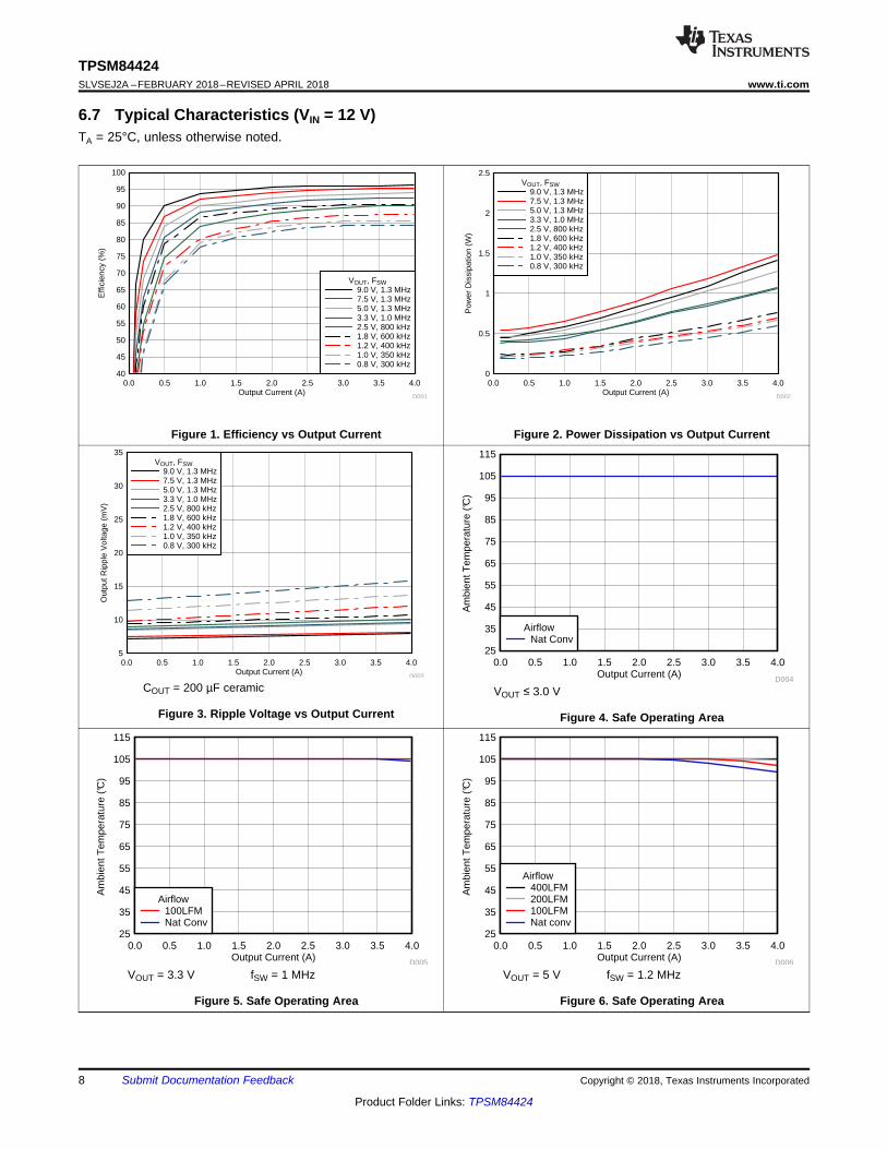
6.7 Typical Characteristics (VIN = 12 V)TA = 25°C, unless otherwise noted.
Figure 1. Efficiency vs Output Current Figure 2. Power Dissipation vs Output Current
COUT = 200 µF ceramic
Figure 3. Ripple Voltage vs Output Current
VOUT ≤ 3.0 V
Figure 4. Safe Operating Area
VOUT = 3.3 V fSW = 1 MHz
Figure 5. Safe Operating Area
VOUT = 5 V fSW = 1.2 MHz
Figure 6. Safe Operating Area
Output Current (A)
Am
bien
t Tem
pera
ture
(°C
)
0.0 0.5 1.0 1.5 2.0 2.5 3.0 3.5 4.025
35
45
55
65
75
85
95
105
115
D010
AirflowNat Conv
Output Current (A)
Out
put R
ippl
e V
olta
ge (
mV
)
0.0 0.5 1.0 1.5 2.0 2.5 3.0 3.5 4.00
5
10
15
20
25
30
35
D009
VOUT, FSW3.3 V, 1.0 MHz2.5 V, 800 kHz1.8 V, 600 kHz1.2 V, 450 kHz1.0 V, 400 kHz0.8 V, 300 kHz
Output Current (A)
Effi
cien
cy (
%)
0.0 0.5 1.0 1.5 2.0 2.5 3.0 3.5 4.040
45
50
55
60
65
70
75
80
85
90
95
100
D007
VOUT, FSW3.3 V, 1.0 MHz2.5 V, 800 kHz1.8 V, 600 kHz1.2 V, 450 kHz1.0 V, 400 kHz0.8 V, 300 kHz
Output Current (A)
Pow
er D
issi
patio
n (W
)
0.0 0.5 1.0 1.5 2.0 2.5 3.0 3.5 4.00
0.2
0.4
0.6
0.8
1
D008
VOUT, FSW3.3 V, 1.0 MHz2.5 V, 800 kHz1.8 V, 600 kHz1.2 V, 450 kHz1.0 V, 400 kHz0.8 V, 300 kHz
9
TPSM84424www.ti.com SLVSEJ2A –FEBRUARY 2018–REVISED APRIL 2018
Product Folder Links: TPSM84424
Submit Documentation FeedbackCopyright © 2018, Texas Instruments Incorporated
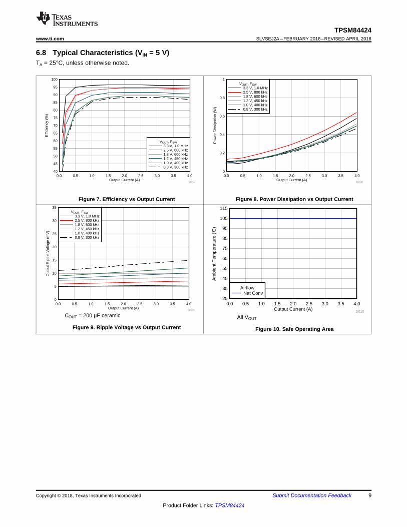
6.8 Typical Characteristics (VIN = 5 V)TA = 25°C, unless otherwise noted.
Figure 7. Efficiency vs Output Current Figure 8. Power Dissipation vs Output Current
COUT = 200 µF ceramic
Figure 9. Ripple Voltage vs Output Current
All VOUT
Figure 10. Safe Operating Area

Copyright © 2018, Texas Instruments Incorporated
PGOOD
VIN
PGND
SW
VOUT
RT/CLK
AGND
EN
SS/TR
FB
TPSM84424
PGOODLogic
5µA
10nF
++
VREF Comp PowerStage and
Control Logic
Thermal Shutdown
ShutdownLogic
OCPVIN
UVLO
Oscillator with PLL
TT
DNC
0.85µH
10
TPSM84424SLVSEJ2A –FEBRUARY 2018–REVISED APRIL 2018 www.ti.com
Product Folder Links: TPSM84424
Submit Documentation Feedback Copyright © 2018, Texas Instruments Incorporated
7 Detailed Description
7.1 OverviewThe TPSM84424 is a full-featured 4.5-V to 17-V input, 4-A, synchronous step-down converter with PWM,MOSFETs, inductor, and control circuitry integrated into a low-profile package. The device integration enablessmall designs, while still leaving the ability to adjust key parameters to meet specific design requirements. TheTPSM84424 provides an output voltage range of 0.6 V to 10 V. An external resistor divider is used to adjust theoutput voltage to the desired output. The switching frequency is also adjustable by using an external resistor or asynchronization clock to accommodate various input and output voltage conditions and to optimize efficiency.
The TPSM84424 includes the TurboTrans feature which optimizes the transient response of the converter whilesimultaneously reducing the quantity of external output capacitors required to meet a target voltage deviationspecification.
The TPSM84424 has been designed for safe start-up into pre-biased loads. The default start up is when VIN istypically 4.1 V. The EN pin has an internal pullup current source that can be used to adjust the input voltageundervoltage lockout (UVLO) with two external resistors. In addition, the internal pullup current of the EN pinallows the device to operate with the EN pin floating. The EN pin can also be pulled low to put the device instandby mode to reduce input quiescent current. The device provides a power-good (PGOOD) signal to indicatewhen the output voltage is within regulation. Thermal shutdown and current limit features protect the deviceduring an overload condition. A 24-pin QFN package that includes exposed bottom pads provides a thermallyenhanced solution for space-constrained applications.
7.2 Functional Block Diagram

AGND
VOUT
FB
RFBT
10 k
RFBB
6RFBB = (k )
(VOUT ± 0.6)
11
TPSM84424www.ti.com SLVSEJ2A –FEBRUARY 2018–REVISED APRIL 2018
Product Folder Links: TPSM84424
Submit Documentation FeedbackCopyright © 2018, Texas Instruments Incorporated
(1) Additional capacitance above the minimum can be ceramic or polymer type.(2) Load transients with > 2 A/µs slew rates may require additional capacitance, see TurboTrans.(3) See Low-ESR Output Capacitors for details on polymer capacitors.
7.3 Feature Description
7.3.1 Adjusting the Output VoltageA resistor divider connected to the FB pin (pin 2) programs the output voltage of the TPSM84424. The outputvoltage adjustment range is from 0.6 V to 10 V. Figure 11 shows the feedback resistor connection for setting theoutput voltage. The recommended value of RFBT is 10 kΩ. The value for RFBB can be calculated using Equation 1or simply selected from the range of values given in Table 1. Table 1 also includes the recommended switchingfrequency and minimum required output capacitance for each output voltage.
(1)
Figure 11. Setting the Output Voltage
Table 1. Standard Component Values
VOUT (V) RFBB (kΩ) RECOMMENDEDfSW (kHz) RRT (kΩ)
Minimum Required COUT(µF) (1) (2)
CERAMIC POLYMER (3)
0.6 open 250 200 400 2200.7 60.4 250 200 400 2200.8 30.1 300 165 300 2200.9 20.0 350 143 200 2201.0 15.0 400 124 200 -1.1 12.1 400 124 200 -1.2 10.0 450 110 200 -1.3 8.66 500 97.6 200 -1.4 7.50 500 97.6 200 -1.5 6.65 550 88.7 150 -1.6 6.04 550 88.7 150 -1.7 5.49 600 82.5 150 -1.8 4.99 600 82.5 100 -1.9 4.64 650 75.0 100 -2.0 4.32 700 69.8 100 -2.5 3.16 800 60.4 100 -3.3 2.21 1000 48.7 47 -5.0 1.37 1200 40.2 47 -6.0 1.10 1200 40.2 47 -7.5 0.866 1300 36.5 47 -9.0 0.715 1300 36.5 22 -10 0.634 1300 36.5 22 -

58650 × fSW (kHz)-1.028 RRT = (k )
12
TPSM84424SLVSEJ2A –FEBRUARY 2018–REVISED APRIL 2018 www.ti.com
Product Folder Links: TPSM84424
Submit Documentation Feedback Copyright © 2018, Texas Instruments Incorporated
7.3.2 Switching Frequency (RT)The switching frequency range of the TPSM84424 is 200 kHz to 1.6 MHz. The switching frequency can easily beset by connecting a resistor (RRT) between the RT pin and AGND. Use Equation 2 to calculate the RRT value fora desired frequency or simply select from Table 2.
The switching frequency must be selected based on the output voltage setting of the device and the operatinginput voltage. See Table 2 for the allowable output voltage range for a given switching frequency.
(2)
Table 2. VOUT Range vs Switching Frequency
SWITCHINGFREQUENCY
VIN = 5 V (±10%) VIN = 12 V (±5%) VIN = 15 V (±5%)VOUT RANGE (V) VOUT RANGE (V) VOUT RANGE (V)
min max min max min max250 kHz 0.6 0.9 0.6 0.8 0.6 0.8300 kHz 0.6 0.9 0.6 0.9 0.7 0.9350 kHz 0.6 1.0 0.7 1.0 0.8 1.0400 kHz 0.6 1.2 0.7 1.2 0.9 1.2450 kHz 0.6 1.8 0.8 1.5 1.0 1.5500 kHz 0.6 2.0 0.9 1.8 1.1 1.8550 kHz 0.6 2.2 1.0 2.0 1.2 2.0600 kHz 0.6 2.5 1.1 2.5 1.4 2.3650 kHz 0.6 3.0 1.2 2.7 1.5 2.5700 kHz 0.6 3.5 1.3 3.0 1.6 2.8750 kHz 0.6 3.5 1.4 3.3 1.7 3.0800 kHz 0.7 3.5 1.5 3.6 1.8 3.3900 kHz 0.7 3.5 1.6 4.0 2.0 4.01.0 MHz 0.9 3.5 1.8 6.0 2.2 4.81.1 MHz 1 3.5 2.0 9.0 2.5 6.01.2 MHz 1.1 3.5 2.2 9.0 2.7 8.01.3 MHz 1.1 3.5 2.3 9.0 2.9 101.4 MHz 1.2 3.5 2.4 9.0 3.1 101.5 MHz 1.3 3.5 2.6 9.0 3.3 101.6 MHz 1.4 3.5 2.8 9.0 3.5 10
7.3.3 Synchronization (CLK)The TPSM84424 switching frequency can also be synchronized to an external clock from 200 kHz to 1.6 MHz.Not all VIN, VOUT, and IOUT conditions can be set to all of the frequencies in this range due to on-time or off-timelimitations. See Table 2 for the allowable operating ranges.
An internal Phase Locked Loop (PLL) has been implemented to allow synchronization and to easily switch fromRT mode to CLK mode. To implement the synchronization feature, connect a square wave clock signal to theRT/CLK pin (pin 24) with a duty cycle from 20% to 80%. The clock signal amplitude must transition lower than0.8 V and higher than 2 V. The start of the switching cycle is synchronized to the falling edge of the RT/CLK pin.
Before the external clock is present the device operates in RT mode and the switching frequency is set by theRT resistor, RRT. Select RRT to set the frequency close to the external synchronization frequency. When theexternal clock is present, the CLK mode overrides the RT mode. The first time the CLK pin is pulled above theRT/CLK high threshold (2 V), the device switches from the RT mode to the CLK mode and the RT/CLK pinbecomes high impedance as the PLL starts to lock onto the frequency of the external clock.
During operation, if the external clock is removed, the internal clock frequency begins to drop. After 10 μs withoutreceiving a clock pulse, the device returns to RT mode. Output undershoot can occur while the switchingfrequency drops and returns to the frequency set by the RT resistor.

13
TPSM84424www.ti.com SLVSEJ2A –FEBRUARY 2018–REVISED APRIL 2018
Product Folder Links: TPSM84424
Submit Documentation FeedbackCopyright © 2018, Texas Instruments Incorporated
(1) Capacitor Supplier Verification, RoHS, Lead-free and Material DetailsConsult capacitor suppliers regarding availability, material composition, RoHS and lead-free status, and manufacturing processrequirements for any capacitors identified in this table.
(2) Specified capacitance values.(3) Maximum ESR @ 100 kHz, 25°C.
7.3.4 Output On/Off Enable (EN)The EN pin provides electrical ON/OFF control of the device. Once the EN pin voltage exceeds the thresholdvoltage, the device starts operation. If the EN pin voltage is pulled below the threshold voltage, the regulatorstops switching and enters low operating current state. The EN pin has an internal pullup current source allowingthe user to float the EN pin for enabling the device.
If an application requires controlling the EN pin, either drive it directly with a logic input or use an opendrain/collector device to interface with the pin. Applying a low voltage to the enable control (EN) pin disables theoutput of the supply, shown in Figure 12. When the EN pin voltage exceeds the threshold voltage, the supplyexecutes a soft-start power-up sequence, as shown in Figure 13.
Figure 12. Enable Turnoff Figure 13. Enable Turnon
7.3.5 Input Capacitor SelectionThe TPSM84424 requires a minimum input capacitance of 20 µF of ceramic type. Use only high-quality ceramictype X5R or X7R capacitors with sufficient voltage rating. TI recommends an additional 100 µF of non-ceramiccapacitancefor applications with transient load requirements. The voltage rating of input capacitors must begreater than the maximum input voltage. To compensate the derating of ceramic capactors, a voltage rating oftwice the maximum input voltage is recommended. At worst case, when operating at 50% duty cycle andmaximum load, the combined ripple current rating of the input capacitors must be at least 2 A(rms). Table 3includes a preferred list of capacitors by vendor.
Table 3. Recommended Input Capacitors (1)
VENDOR SERIES PART NUMBERCAPACITOR CHARACTERISTICS
WORKING VOLTAGE (V) CAPACITANCE (2)
(µF)ESR (3)
(mΩ)
TDK X7R C3225X7R1E106K250AC 25 10 2
Murata X7R GRM32DR71E106KA12L 25 10 2
Panasonic ZA EEHZA1H101P 50 100 28
Panasonic FC EEUFC1H101B 50 100 162

14
TPSM84424SLVSEJ2A –FEBRUARY 2018–REVISED APRIL 2018 www.ti.com
Product Folder Links: TPSM84424
Submit Documentation Feedback Copyright © 2018, Texas Instruments Incorporated
(1) Capacitor Supplier Verification, RoHS, Lead-free and Material DetailsConsult capacitor suppliers regarding availability, material composition, RoHS and lead-free status, and manufacturing processrequirements for any capacitors identified in this table.
(2) Specified capacitance values.(3) Maximum ESR @ 100 kHz, 25°C.
7.3.6 Output Capacitor SelectionThe minimum required output capacitance of the TPSM84424 is a function of the output voltage and is shown inTable 1. The required capacitance can be comprised of all ceramic capacitors or a combination of ceramic andlow-ESR polymer type capacitors. When adding additional capacitors, low-ESR capacitors like the onesrecommended in Low-ESR Output Capacitors are required. The required capacitance above the minimum isdetermined by actual transient deviation requirements. See TurboTrans (TT) for typical transient response valuesfor several output voltage and capacitance combinations. See Table 4 for recommended output capacitors.
Table 4. Recommended Output Capacitors (1)
VENDOR SERIES PART NUMBERCAPACITOR CHARACTERISTICS
WORKINGVOLTAGE (V)
CAPACITANCE (2)
(µF)ESR (3)
(mΩ)
TDK X7R C3225X7R1C226K 16 22 2
Murata X7R GCJ32ER71C226K 16 22 2
TDK X5R C3225X5R1C226M 16 22 2
Murata X5R GRM32ER61C226K 16 22 2
Murata X7R GCM32ER70J476K 6.3 47 2
Murata X7R GRM32ER71A476K 10 47 2
Murata X5R GRM32ER61C476K 16 47 3
TDK X5R C3225X5R0J107M 6.3 100 2
Murata X5R GRM32ER60J107M 6.3 100 2
Murata X5R GRM32ER61A107M 10 100 2
Panasonic POSCAP 4TPE220MF 4.0 220 15
Kemet T520 T520D227M006ATE015 6.3 220 15
Panasonic POSCAP 6TPE330MAA 6.3 330 10
Kemet T520 T520D337M006ATE010 6.3 330 10
Panasonic POSCAP 2R5TPE470M7 2.5 470 7
Kemet T520 T520D477M2R5ATE007 2.5 470 7
KTT × VOUT × CO(eff)(µF) RTT = (k )( )50
-2[ ]
15
TPSM84424www.ti.com SLVSEJ2A –FEBRUARY 2018–REVISED APRIL 2018
Product Folder Links: TPSM84424
Submit Documentation FeedbackCopyright © 2018, Texas Instruments Incorporated
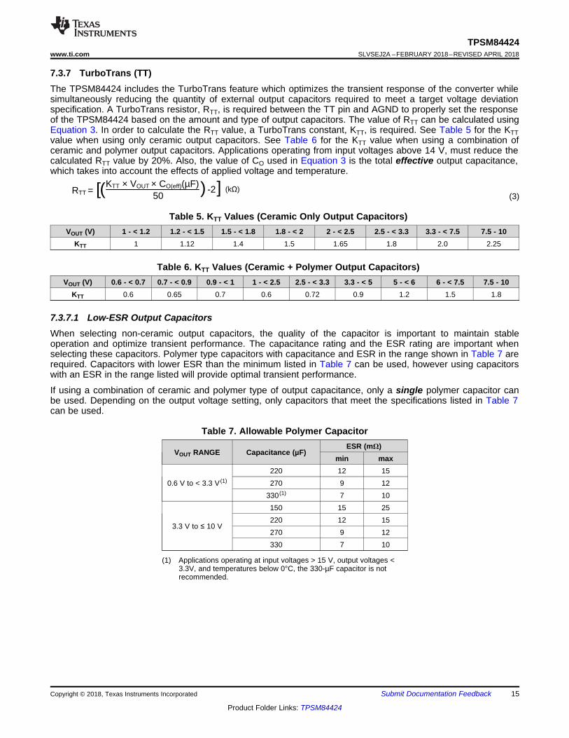
7.3.7 TurboTrans (TT)The TPSM84424 includes the TurboTrans feature which optimizes the transient response of the converter whilesimultaneously reducing the quantity of external output capacitors required to meet a target voltage deviationspecification. A TurboTrans resistor, RTT, is required between the TT pin and AGND to properly set the responseof the TPSM84424 based on the amount and type of output capacitors. The value of RTT can be calculated usingEquation 3. In order to calculate the RTT value, a TurboTrans constant, KTT, is required. See Table 5 for the KTTvalue when using only ceramic output capacitors. See Table 6 for the KTT value when using a combination ofceramic and polymer output capacitors. Applications operating from input voltages above 14 V, must reduce thecalculated RTT value by 20%. Also, the value of CO used in Equation 3 is the total effective output capacitance,which takes into account the effects of applied voltage and temperature.
(3)
Table 5. KTT Values (Ceramic Only Output Capacitors)VOUT (V) 1 - < 1.2 1.2 - < 1.5 1.5 - < 1.8 1.8 - < 2 2 - < 2.5 2.5 - < 3.3 3.3 - < 7.5 7.5 - 10
KTT 1 1.12 1.4 1.5 1.65 1.8 2.0 2.25
Table 6. KTT Values (Ceramic + Polymer Output Capacitors)VOUT (V) 0.6 - < 0.7 0.7 - < 0.9 0.9 - < 1 1 - < 2.5 2.5 - < 3.3 3.3 - < 5 5 - < 6 6 - < 7.5 7.5 - 10
KTT 0.6 0.65 0.7 0.6 0.72 0.9 1.2 1.5 1.8
7.3.7.1 Low-ESR Output CapacitorsWhen selecting non-ceramic output capacitors, the quality of the capacitor is important to maintain stableoperation and optimize transient performance. The capacitance rating and the ESR rating are important whenselecting these capacitors. Polymer type capacitors with capacitance and ESR in the range shown in Table 7 arerequired. Capacitors with lower ESR than the minimum listed in Table 7 can be used, however using capacitorswith an ESR in the range listed will provide optimal transient performance.
If using a combination of ceramic and polymer type of output capacitance, only a single polymer capacitor canbe used. Depending on the output voltage setting, only capacitors that meet the specifications listed in Table 7can be used.
(1) Applications operating at input voltages > 15 V, output voltages <3.3V, and temperatures below 0°C, the 330-µF capacitor is notrecommended.
Table 7. Allowable Polymer Capacitor
VOUT RANGE Capacitance (µF)ESR (mΩ)
min max
0.6 V to < 3.3 V (1)
220 12 15270 9 12
330 (1) 7 10
3.3 V to ≤ 10 V
150 15 25220 12 15270 9 12330 7 10

16
TPSM84424SLVSEJ2A –FEBRUARY 2018–REVISED APRIL 2018 www.ti.com
Product Folder Links: TPSM84424
Submit Documentation Feedback Copyright © 2018, Texas Instruments Incorporated
(1) Load step slew rate of 2 A/µs(2) Load step slew rate of 1 A/µs
7.3.7.2 Transient ResponseThe TPSM84424 transient response is listed in Table 8 for several common output voltages with differentcapacitor combinations. The calculated RTT value is included in the table along with the typical voltage deviationfor a 1 A and 2 A load step. All data was taken at the recommended switching frequency for each output voltage.
Table 8. Output Voltage Transient ResponseVIN = 12 V, CIN1 = 2x 10 µF Ceramic, CIN2 = 100 µF Electrolytic, TA = 25°C
VOUT (V) COUT1 Ceramic COUT2 BULK RTT (kΩ)VOLTAGE DEVIATION
1 A LOAD STEP 2 A LOAD STEP
0.8 (1) 300 µF 220 µF 3.40 11 mV . (1.4%) 22 mV . (2.7%)400 µF 330 µF 5.36 9 mV . (1.1%) 18 mV . (2.2%)
1 (1)
200 µF - 2.00 15 mV . (1.5%) 30 mV . (3%)200 µF 220 µF 3.01 12 mV . (1.2%) 24 mV . (2.4%)400 µF - 6.04 11 mV . (1.1%) 23 mV . (2.3%)400 µF 220 µF 5.49 10 mV . (1.0%) 20 mV . (2%)
1.2 (1)
200 µF - 3.40 17 mV . (1.4%) 35 mV . (2.9%)200 µF 220 µF 4.02 13 mV . (1.1%) 27 mV . (2.2%)400 µF - 8.87 11 mV . (0.9%) 22 mV . (1.8%)400 µF 220 µF 6.98 9 mV . (0.8%) 18 mV . (1.5%)
1.8 (1)
100 µF - 3.40 27 mV . (1.6%) 56 mV . (3.1%)300 µF - 14.3 11 mV . (0.6%) 22 mV . (1.2%)100 µF 220 µF 4.87 12 mV . (0.7%) 24 mV . (1.3%)
3.3 (2)
100 µF - 8.66 30 mV . (0.9%) 60 mV . (1.8%)100 µF 220 µF 31.6 16 mV . (0.5%) 32 mV . (1.0%)200 µF - 19.1 22 mV . (0.7%) 43 mV . (1.3%)
5 (2)
100 µF - 10.0 42 mV . (0.9%) 83 mV . (1.7%)100 µF 220 µF 31.6 16 mV . (0.3%) 32 mV . (0.6%)200 µF - 22.1 24 mV . (0.5%) 48 mV . (1%)
7.5 (2) 100 µF - 10.5 56 mV . (0.8%) 112 mV . (1.5%)47 µF 220 µF 28.0 18 mV . (0.3%) 36 mV . (0.5%)

17
TPSM84424www.ti.com SLVSEJ2A –FEBRUARY 2018–REVISED APRIL 2018
Product Folder Links: TPSM84424
Submit Documentation FeedbackCopyright © 2018, Texas Instruments Incorporated
7.3.7.2.1 Transient Waveforms (VIN = 12 V)
VOUT = 0.8 V COUT = 300 µF ceramic + 220 µF polymer
Figure 14. VOUT = 0.8 V, 2-A Load Step
VOUT = 0.8 V COUT = 300 µF ceramic + 330 µF polymer
Figure 15. VOUT = 0.8 V, 2-A Load Step
VOUT = 1 V COUT = 400 µF ceramic
Figure 16. VOUT = 1 V, 2-A Load Step
VOUT = 1 V COUT = 200 µF ceramic + 220 µF polymer
Figure 17. VOUT = 1 V, 2-A Load Step
VOUT = 1.2 V COUT = 200 µF ceramic
Figure 18. VOUT = 1.2 V, 2-A Load Step
VOUT = 1.2 V COUT = 200 µF ceramic + 220 µF polymer
Figure 19. VOUT = 1.2 V, 2-A Load Step
0.6V × (CSS + 10nF)tSS = 5 µA
EN
PGND
RUVLO1
RUVLO2
VIN
18
TPSM84424SLVSEJ2A –FEBRUARY 2018–REVISED APRIL 2018 www.ti.com
Product Folder Links: TPSM84424
Submit Documentation Feedback Copyright © 2018, Texas Instruments Incorporated
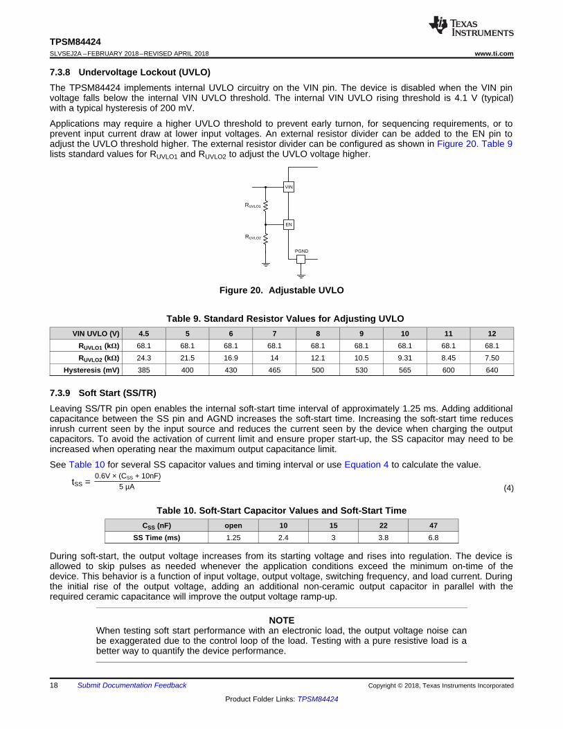
7.3.8 Undervoltage Lockout (UVLO)The TPSM84424 implements internal UVLO circuitry on the VIN pin. The device is disabled when the VIN pinvoltage falls below the internal VIN UVLO threshold. The internal VIN UVLO rising threshold is 4.1 V (typical)with a typical hysteresis of 200 mV.
Applications may require a higher UVLO threshold to prevent early turnon, for sequencing requirements, or toprevent input current draw at lower input voltages. An external resistor divider can be added to the EN pin toadjust the UVLO threshold higher. The external resistor divider can be configured as shown in Figure 20. Table 9lists standard values for RUVLO1 and RUVLO2 to adjust the UVLO voltage higher.
Figure 20. Adjustable UVLO
Table 9. Standard Resistor Values for Adjusting UVLOVIN UVLO (V) 4.5 5 6 7 8 9 10 11 12
RUVLO1 (kΩ) 68.1 68.1 68.1 68.1 68.1 68.1 68.1 68.1 68.1RUVLO2 (kΩ) 24.3 21.5 16.9 14 12.1 10.5 9.31 8.45 7.50
Hysteresis (mV) 385 400 430 465 500 530 565 600 640
7.3.9 Soft Start (SS/TR)Leaving SS/TR pin open enables the internal soft-start time interval of approximately 1.25 ms. Adding additionalcapacitance between the SS pin and AGND increases the soft-start time. Increasing the soft-start time reducesinrush current seen by the input source and reduces the current seen by the device when charging the outputcapacitors. To avoid the activation of current limit and ensure proper start-up, the SS capacitor may need to beincreased when operating near the maximum output capacitance limit.
See Table 10 for several SS capacitor values and timing interval or use Equation 4 to calculate the value.
(4)
Table 10. Soft-Start Capacitor Values and Soft-Start TimeCSS (nF) open 10 15 22 47
SS Time (ms) 1.25 2.4 3 3.8 6.8
During soft-start, the output voltage increases from its starting voltage and rises into regulation. The device isallowed to skip pulses as needed whenever the application conditions exceed the minimum on-time of thedevice. This behavior is a function of input voltage, output voltage, switching frequency, and load current. Duringthe initial rise of the output voltage, adding an additional non-ceramic output capacitor in parallel with therequired ceramic capacitance will improve the output voltage ramp-up.
NOTEWhen testing soft start performance with an electronic load, the output voltage noise canbe exaggerated due to the control loop of the load. Testing with a pure resistive load is abetter way to quantify the device performance.
EN
VOUT
SS/TR
EN
VOUT
VOUT1
R1
R2
VOUT2
R2 = 0.6 × R1
(k )(VOUT2 ± 0.6)
(VOUT2 × 5)R1 =
0.6(k )
EN
PGOOD
VOUTVOUT1
EN
PGOOD
VOUTVOUT2
19
TPSM84424www.ti.com SLVSEJ2A –FEBRUARY 2018–REVISED APRIL 2018
Product Folder Links: TPSM84424
Submit Documentation FeedbackCopyright © 2018, Texas Instruments Incorporated
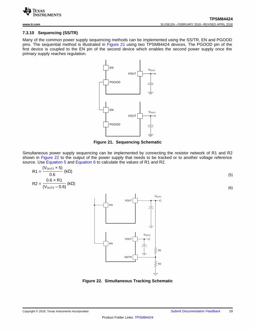
7.3.10 Sequencing (SS/TR)Many of the common power supply sequencing methods can be implemented using the SS/TR, EN and PGOODpins. The sequential method is illustrated in Figure 21 using two TPSM84424 devices. The PGOOD pin of thefirst device is coupled to the EN pin of the second device which enables the second power supply once theprimary supply reaches regulation.
Figure 21. Sequencing Schematic
Simultaneous power supply sequencing can be implemented by connecting the resistor network of R1 and R2shown in Figure 22 to the output of the power supply that needs to be tracked or to another voltage referencesource. Use Equation 5 and Equation 6 to calculate the values of R1 and R2.
(5)
(6)
Figure 22. Simultaneous Tracking Schematic

20
TPSM84424SLVSEJ2A –FEBRUARY 2018–REVISED APRIL 2018 www.ti.com
Product Folder Links: TPSM84424
Submit Documentation Feedback Copyright © 2018, Texas Instruments Incorporated
7.3.11 Power Good (PGOOD)The PGOOD pin is an open-drain output requiring an external pullup resistor to output a high signal. Once theoutput voltage is between 91% and 106% of the setpoint voltage and SS/TR is greater than 0.75 V, the PGOODpin pulldown is released and the pin floats. A pullup resistor between the values of 10 kΩ and 100 kΩ to avoltage source of 6.5 V or less is recommended. The PGOOD pin is pulled low when the output voltage is lowerthan 89% or greater than 108% of the setpoint voltage.
7.3.12 Safe Start-up into Pre-Biased OutputsThe device has been designed to prevent the low-side MOSFET from discharging a pre-biased output. Duringmonotonic pre-biased start-up, the low-side MOSFET is not allowed to sink current until the SS/TR pin voltage ishigher than the FB pin voltage and the high-side MOSFET begins to switch.
7.3.13 Overcurrent ProtectionFor protection against load faults, the TPSM84424 is protected from overcurrent conditions by cycle-by-cyclecurrent limiting. In an extended overcurrent condition the device enters hiccup mode to reduce power dissipation.In hiccup mode, the module continues in a cycle of successive shutdown and power up until the load fault isremoved. During this period, the average current flowing into the fault is significantly reduced, which reducespower dissipation. Once the fault is removed, the module automatically recovers and returns to normal operation.
7.3.14 Thermal ShutdownThe internal thermal shutdown circuitry forces the device to stop switching if the junction temperature exceeds170°C typically. The device reinitiates the power up sequence when the junction temperature drops below 155°Ctypically.
7.4 Device Functional Modes
7.4.1 Active ModeThe TPSM84424 is in active mode when VIN is above the UVLO threshold and the EN pin voltage is above theEN high threshold. The EN pin has an internal current source to enable the output when the EN pin is leftfloating. If the EN pin is pulled low the device is put into a low quiescent current state.
7.4.2 Shutdown ModeThe EN pin provides electrical ON and OFF control for the TPSM84424. When the EN pin voltage is below theEN low threshold, the device is in shutdown mode. In shutdown mode the device is put into a low quiescentcurrent state. The TPSM84424 also employs undervoltage lockout protection. If VIN is below the UVLO level, theoutput of the regulator turns off.

VIN
PGND
VIN = 12V
VOUTVOUT = 1.2 V
FB
10 kO
PGOOD
EN
RT/CLK
TPSM84424
AGND
TT
10 µF
25 V
10 µF
25 V
110 kO 4.12 kO 10 kO
100 µF
6.3 V
100 µF
6.3 V
220 µF
15 mO
Copyright © 2018, Texas Instruments Incorporated
21
TPSM84424www.ti.com SLVSEJ2A –FEBRUARY 2018–REVISED APRIL 2018
Product Folder Links: TPSM84424
Submit Documentation FeedbackCopyright © 2018, Texas Instruments Incorporated
8 Application and Implementation
NOTEInformation in the following applications sections is not part of the TI componentspecification, and TI does not warrant its accuracy or completeness. TI’s customers areresponsible for determining suitability of components for their purposes. Customers shouldvalidate and test their design implementation to confirm system functionality.
8.1 Application InformationThe TPSM84424 is a fixed-frequency, synchronous step-down DC-DC power module. It is used to convert ahigher DC voltage to a lower DC voltage with a maximum output current of 4 A. The following design procedurecan be used to select components for the TPSM84424. Alternately, the WEBENCH® software may be used togenerate complete designs. When generating a design, the WEBENCH software utilizes an iterative designprocedure and accesses comprehensive databases of components. See www.ti.com/webench for more details.
8.2 Typical ApplicationThe TPSM84424 requires only a few external components to convert from a wide input voltage supply range to awide range of output voltages. Figure 23 shows a typical TPSM84424 schematic with only the minimum requiredcomponents.
Figure 23. TPSM84424 Typical Application
8.2.1 Design RequirementsFor this design example, use the parameters listed in Table 11 and follow the design procedures below.
Table 11. Design Example ParametersDESIGN PARAMETER VALUE
Input voltage VIN 12 V typicalOutput voltage VOUT 1.2 VOutput current rating 4 A
Key care-abouts Small solution size, good transient responseTransient response requirements 3% voltage deviation, 2-A load step, 1-A/µs slew rate

KTT × VOUT × CO(eff)(µF) RTT = (k )( )50
-2[ ]
58650 × fSW (kHz)-1.028 RRT = (k )
6RFBB = (k )
(VOUT ± 0.6)
22
TPSM84424SLVSEJ2A –FEBRUARY 2018–REVISED APRIL 2018 www.ti.com
Product Folder Links: TPSM84424
Submit Documentation Feedback Copyright © 2018, Texas Instruments Incorporated
8.2.2 Detailed Design Procedure
8.2.2.1 Custom Design With WEBENCH® ToolsClick here to create a custom design using the TPSM84424 device with the WEBENCH® Power Designer.1. Start by entering the input voltage (VIN), output voltage (VOUT), and output current (IOUT) requirements.2. Optimize the design for key parameters such as efficiency, footprint, and cost using the optimizer dial.3. Compare the generated design with other possible solutions from Texas Instruments.
The WEBENCH Power Designer provides a customized schematic along with a list of materials with real-timepricing and component availability.
In most cases, these actions are available:• Run electrical simulations to see important waveforms and circuit performance• Run thermal simulations to understand board thermal performance• Export customized schematic and layout into popular CAD formats• Print PDF reports for the design, and share the design with colleagues
Get more information about WEBENCH tools at www.ti.com/WEBENCH.
8.2.2.2 Output Voltage SetpointThe output voltage of the TPSM84424 device is externally adjustable using a two resistor divider (RFBT andRFBB). The recommended value of RFBT is 10 kΩ. Select the value of RFBB from Table 1 or calculate usingEquation 7:
(7)
To set the output voltage to 1.2 V, the RFBB value is 10 kΩ.
8.2.2.3 Setting the Switching FrequencyTo set the switching frequency of the TPSM84424 a resistor (RRT) between the RT/CLK pin and AGND isrequired. Select the value of RRT from Table 1 or calculate using Equation 8:
(8)
The recommended switching frequncy for a 1.2 V output is 450 kHz. To set the switching frequency to 450 kHz,the RRT value is 110 kΩ.
8.2.2.4 Input CapacitorsFor this design, two 10-μF ceramic capacitors rated for 25 V are used for the input decoupling capacitors.
8.2.2.5 Output CapacitorsThe minimum required output capacitance for a 1.2-V output is 200 μF of ceramic capacitance, as listed inTable 1. For this design, two 100-μF ceramic capacitors plus a 220 μF, 15 mΩ polymer capacitor where used tomeet the transient requirement specification.
8.2.2.6 TurboTrans ResistorA TurboTrans resistor (RTT) is required between the TT pin and AGND. The value of RTT can be calulated usingEquation 9. When calculating the RTT value, the total effective output capacitance which takes into account theeffects of applied voltage and temperature.
(9)
The calulated value for RTT for this application is 4.12 kΩ.

23
TPSM84424www.ti.com SLVSEJ2A –FEBRUARY 2018–REVISED APRIL 2018
Product Folder Links: TPSM84424
Submit Documentation FeedbackCopyright © 2018, Texas Instruments Incorporated
8.2.2.7 Application Waveforms
Figure 24. Output Ripple and SW Waveforms Figure 25. Transient Response Waveforms
9 Power Supply RecommendationsThe TPSM84424 is designed to operate from an input voltage supply range between 4.5 V and 17 V. This inputsupply must be well regulated and able to withstand maximum input current and maintain a stable voltage. Theresistance of the input supply rail must be low enough that an input current transient does not cause a highenough drop at the TPSM84424 supply voltage that can cause a false UVLO fault triggering and system reset.
If the input supply is located more than a few inches from the TPSM84424 additional bulk capacitance may berequired in addition to the ceramic bypass capacitors. Typically, a 47-µF or 100-μF electrolytic capacitor willsuffice.

24
TPSM84424SLVSEJ2A –FEBRUARY 2018–REVISED APRIL 2018 www.ti.com
Product Folder Links: TPSM84424
Submit Documentation Feedback Copyright © 2018, Texas Instruments Incorporated
10 LayoutThe performance of any switching power supply depends as much upon the layout of the PCB as the componentselection. The following guidelines will help users design a PCB with the best power conversion performance,thermal performance, and minimized generation of unwanted EMI.
10.1 Layout GuidelinesTo achieve optimal electrical and thermal performance, an optimized PCB layout is required. Figure 26 thruFigure 29, shows a typical PCB layout. Some considerations for an optimized layout are:• Use large copper areas for power planes (VIN, VOUT, and PGND) to minimize conduction loss and thermal
stress.• Place ceramic input and output capacitors close to the device pins to minimize high frequency noise.• Locate additional output capacitors between the ceramic capacitor and the load.• Keep AGND and PGND separate from one another. The connection is made internal to the device.• Place RFBB, RRT, and CSS as close as possible to their respective pins.• Use multiple vias to connect the power planes (VIN, VOUT, and PGND) to internal layers.
10.2 Layout Examples
Figure 26. Typical Top-Layer Layout Figure 27. Typical Layer-2 Layout
Figure 28. Typical Layer-3 Layout Figure 29. Typical Bottom-Layer Layout (Bottom View)

25
TPSM84424www.ti.com SLVSEJ2A –FEBRUARY 2018–REVISED APRIL 2018
Product Folder Links: TPSM84424
Submit Documentation FeedbackCopyright © 2018, Texas Instruments Incorporated
10.3 EMIThe TPSM84424 is compliant with EN55011 Class B radiated emissions. Figure 30 and Figure 31 show typicalexamples of radiated emissions plots for the TPSM84424. The graphs include the plots of the antenna in thehorizontal and vertical positions.
10.3.1 EMI PlotsEMI plots were measured using the standard TPSM84424EVM with no input filter.
Figure 30. Radiated Emissions 12-V Input, 1.2-V Output, 4-A Load (EN55011 Class B)
Figure 31. Radiated Emissions 12-V Input, 5-V Output, 4-A Load (EN55011 Class B)
26
TPSM84424SLVSEJ2A –FEBRUARY 2018–REVISED APRIL 2018 www.ti.com
Product Folder Links: TPSM84424
Submit Documentation Feedback Copyright © 2018, Texas Instruments Incorporated
10.4 Package Specifications
TPSM84424 VALUE UNITWeight 0.90 gramsFlammability Meets UL 94 V-OMTBF Calculated Reliability Per Bellcore TR-332, 50% stress, TA = 40°C, ground benign 73.5 MHrs

27
TPSM84424www.ti.com SLVSEJ2A –FEBRUARY 2018–REVISED APRIL 2018
Product Folder Links: TPSM84424
Submit Documentation FeedbackCopyright © 2018, Texas Instruments Incorporated
11 Device and Documentation Support
11.1 Device Support
11.1.1 Third-Party Products DisclaimerTI'S PUBLICATION OF INFORMATION REGARDING THIRD-PARTY PRODUCTS OR SERVICES DOES NOTCONSTITUTE AN ENDORSEMENT REGARDING THE SUITABILITY OF SUCH PRODUCTS OR SERVICESOR A WARRANTY, REPRESENTATION OR ENDORSEMENT OF SUCH PRODUCTS OR SERVICES, EITHERALONE OR IN COMBINATION WITH ANY TI PRODUCT OR SERVICE.
11.2 Development Support
11.2.1 Custom Design With WEBENCH® ToolsClick here to create a custom design using the TPSM84424 device with the WEBENCH® Power Designer.1. Start by entering the input voltage (VIN), output voltage (VOUT), and output current (IOUT) requirements.2. Optimize the design for key parameters such as efficiency, footprint, and cost using the optimizer dial.3. Compare the generated design with other possible solutions from Texas Instruments.
The WEBENCH Power Designer provides a customized schematic along with a list of materials with real-timepricing and component availability.
In most cases, these actions are available:• Run electrical simulations to see important waveforms and circuit performance• Run thermal simulations to understand board thermal performance• Export customized schematic and layout into popular CAD formats• Print PDF reports for the design, and share the design with colleagues
Get more information about WEBENCH tools at www.ti.com/WEBENCH.
11.3 Receiving Notification of Documentation UpdatesTo receive notification of documentation updates, navigate to the device product folder on ti.com. In the upperright corner, click on Alert me to register and receive a weekly digest of any product information that haschanged. For change details, review the revision history included in any revised document.
11.4 Community ResourcesThe following links connect to TI community resources. Linked contents are provided "AS IS" by the respectivecontributors. They do not constitute TI specifications and do not necessarily reflect TI's views; see TI's Terms ofUse.
TI E2E™ Online Community TI's Engineer-to-Engineer (E2E) Community. Created to foster collaborationamong engineers. At e2e.ti.com, you can ask questions, share knowledge, explore ideas and helpsolve problems with fellow engineers.
Design Support TI's Design Support Quickly find helpful E2E forums along with design support tools andcontact information for technical support.
11.5 TrademarksTurboTrans, E2E are trademarks of Texas Instruments.WEBENCH is a registered trademark of Texas Instruments.
11.6 Electrostatic Discharge CautionThese devices have limited built-in ESD protection. The leads should be shorted together or the device placed in conductive foamduring storage or handling to prevent electrostatic damage to the MOS gates.

Reel Width (W1)
REEL DIMENSIONS
A0
B0
K0
W
Dimension designed to accommodate the component length
Dimension designed to accommodate the component thickness
Overall width of the carrier tape
Pitch between successive cavity centers
Dimension designed to accommodate the component width
TAPE DIMENSIONS
K0 P1
B0 W
A0Cavity
QUADRANT ASSIGNMENTS FOR PIN 1 ORIENTATION IN TAPE
Pocket Quadrants
Sprocket Holes
Q1 Q1Q2 Q2
Q3 Q3Q4 Q4
ReelDiameter
User Direction of Feed
P1
28
TPSM84424SLVSEJ2A –FEBRUARY 2018–REVISED APRIL 2018 www.ti.com
Product Folder Links: TPSM84424
Submit Documentation Feedback Copyright © 2018, Texas Instruments Incorporated
11.7 GlossarySLYZ022 — TI Glossary.
This glossary lists and explains terms, acronyms, and definitions.
12 Mechanical, Packaging, and Orderable InformationThe following pages include mechanical packaging and orderable information. This information is the mostcurrent data available for the designated devices. This data is subject to change without notice and revision ofthis document. For browser-based versions of this data sheet, refer to the left-hand navigation.
12.1 Tape and Reel Information
Device PackageType
PackageDrawing Pins SPQ
ReelDiameter
(mm)
ReelWidth W1
(mm)
A0(mm)
B0(mm)
K0(mm)
P1(mm)
W(mm)
Pin1Quadrant
TPSM84424MOLR QFM MOL 24 500 330.0 16.0 7.8 7.8 5.81 12.0 16.0 Q2
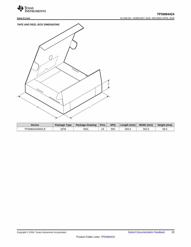
TAPE AND REEL BOX DIMENSIONS
Width (mm)
WL
H
29
TPSM84424www.ti.com SLVSEJ2A –FEBRUARY 2018–REVISED APRIL 2018
Product Folder Links: TPSM84424
Submit Documentation FeedbackCopyright © 2018, Texas Instruments Incorporated
Device Package Type Package Drawing Pins SPQ Length (mm) Width (mm) Height (mm)TPSM84424MOLR QFM MOL 24 500 383.0 353.0 58.0

PACKAGE OPTION ADDENDUM
www.ti.com 22-May-2019
Addendum-Page 1
PACKAGING INFORMATION
Orderable Device Status(1)
Package Type PackageDrawing
Pins PackageQty
Eco Plan(2)
Lead/Ball Finish(6)
MSL Peak Temp(3)
Op Temp (°C) Device Marking(4/5)
Samples
TPSM84424MOLR ACTIVE QFM MOL 24 500 RoHS Exempt& Green
NIAU Level-3-260C-168 HR -40 to 105 TPSM84424
(1) The marketing status values are defined as follows:ACTIVE: Product device recommended for new designs.LIFEBUY: TI has announced that the device will be discontinued, and a lifetime-buy period is in effect.NRND: Not recommended for new designs. Device is in production to support existing customers, but TI does not recommend using this part in a new design.PREVIEW: Device has been announced but is not in production. Samples may or may not be available.OBSOLETE: TI has discontinued the production of the device.
(2) RoHS: TI defines "RoHS" to mean semiconductor products that are compliant with the current EU RoHS requirements for all 10 RoHS substances, including the requirement that RoHS substancedo not exceed 0.1% by weight in homogeneous materials. Where designed to be soldered at high temperatures, "RoHS" products are suitable for use in specified lead-free processes. TI mayreference these types of products as "Pb-Free".RoHS Exempt: TI defines "RoHS Exempt" to mean products that contain lead but are compliant with EU RoHS pursuant to a specific EU RoHS exemption.Green: TI defines "Green" to mean the content of Chlorine (Cl) and Bromine (Br) based flame retardants meet JS709B low halogen requirements of <=1000ppm threshold. Antimony trioxide basedflame retardants must also meet the <=1000ppm threshold requirement.
(3) MSL, Peak Temp. - The Moisture Sensitivity Level rating according to the JEDEC industry standard classifications, and peak solder temperature.
(4) There may be additional marking, which relates to the logo, the lot trace code information, or the environmental category on the device.
(5) Multiple Device Markings will be inside parentheses. Only one Device Marking contained in parentheses and separated by a "~" will appear on a device. If a line is indented then it is a continuationof the previous line and the two combined represent the entire Device Marking for that device.
(6) Lead/Ball Finish - Orderable Devices may have multiple material finish options. Finish options are separated by a vertical ruled line. Lead/Ball Finish values may wrap to two lines if the finishvalue exceeds the maximum column width.
Important Information and Disclaimer:The information provided on this page represents TI's knowledge and belief as of the date that it is provided. TI bases its knowledge and belief on informationprovided by third parties, and makes no representation or warranty as to the accuracy of such information. Efforts are underway to better integrate information from third parties. TI has taken andcontinues to take reasonable steps to provide representative and accurate information but may not have conducted destructive testing or chemical analysis on incoming materials and chemicals.TI and TI suppliers consider certain information to be proprietary, and thus CAS numbers and other limited information may not be available for release.
In no event shall TI's liability arising out of such information exceed the total purchase price of the TI part(s) at issue in this document sold by TI to Customer on an annual basis.

www.ti.com
PACKAGE OUTLINE
C
5.4 MAX
4X 1.61.4
20X 1.10.9
16X 0.450.25
4X 3.43.2
4X 1.41.2
12X 0.65
2X3.25
2X 0.15
2X 1.6
2X5.9
4X2.05
6.4
2X 1.425
6.4
B 7.67.4
A
7.67.4
(0.05) TYP
4223723/A 05/2017
QFM - 5.4 mm max heightMOL0024AQUAD FLAT MODULE
NOTES: 1. All linear dimensions are in millimeters. Any dimensions in parenthesis are for reference only. Dimensioning and tolerancing per ASME Y14.5M. 2. This drawing is subject to change without notice. 3. The package thermal pads must be soldered to the printed circuit board for optimal thermal and mechanical performance.
SCALE 1.500
INDEX AREAPIN 1
SEATING PLANE
0.08 C
SYMM
0.1 C A B0.05
PKG
1
8
13
20
12
2224
ALL PADS
(OPTIONAL)PIN 1 ID
www.ti.com
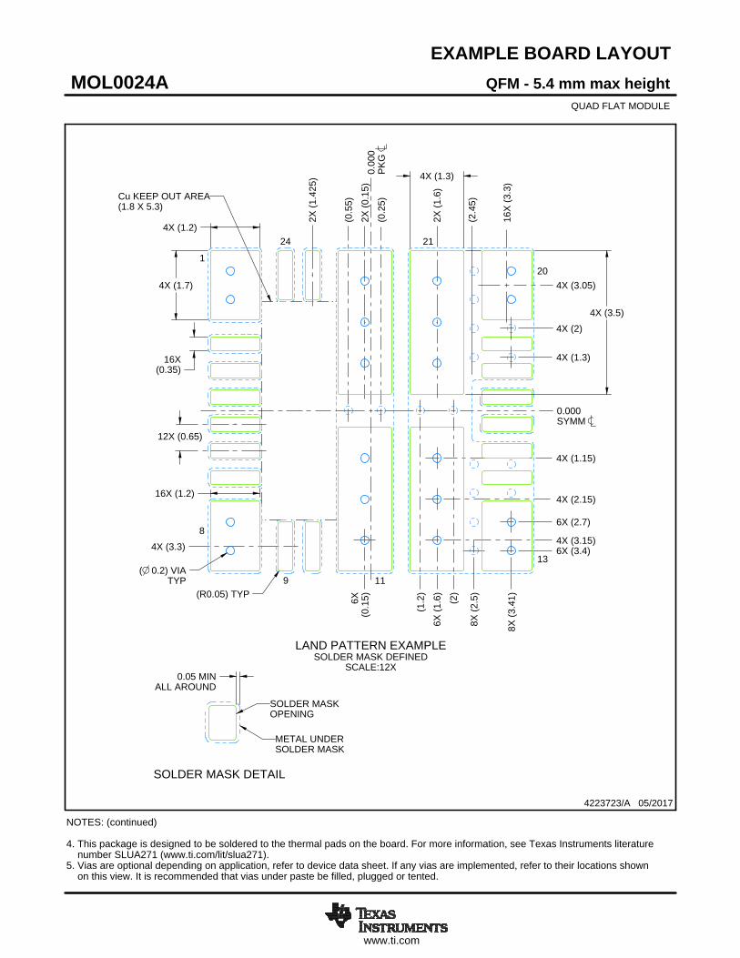
EXAMPLE BOARD LAYOUT
0.05 MINALL AROUND
.000SYMM 0
4X ( )1.3
4X ( )2.15
6X ( )2.7
4X ( )3.15
4X ( )3.05
6X ( )3.44X ( )3.3
.000
PK
G
02X
()
0.15
2X (
)1.
6
()
2.45
()
0.25
()
0.55
16X
()
3.3
6X(
)0.
15 ()
1.2
6X (
)1.
6 ()2
4X ( )1.158X
()
2.5
8X (
)3.
41
4X (1.2)
4X (1.7)
16X(0.35)
12X (0.65)
4X (3.5)
16X (1.2)
4X ( )2
2X (
)1.
425
( 0.2) VIATYP
(R0.05) TYP
4X (1.3)
4223723/A 05/2017
QFM - 5.4 mm max heightMOL0024AQUAD FLAT MODULE
NOTES: (continued) 4. This package is designed to be soldered to the thermal pads on the board. For more information, see Texas Instruments literature number SLUA271 (www.ti.com/lit/slua271).5. Vias are optional depending on application, refer to device data sheet. If any vias are implemented, refer to their locations shown on this view. It is recommended that vias under paste be filled, plugged or tented.
SOLDER MASKOPENING
METAL UNDERSOLDER MASK
SOLDER MASK DETAIL
LAND PATTERN EXAMPLESOLDER MASK DEFINED
SCALE:12X
Cu KEEP OUT AREA(1.8 X 5.3)
1
8
9
13
20
24 21
11

www.ti.com
EXAMPLE STENCIL DESIGN
16X (0.65)
16X (1.2)
4X (1.1)
12X (1.6)
16X (0.35)
8X (1.2)
2X (1.425)
4X (0.15)
4X (1.6)
16X (3.3)
8X (3.05)
4X (3.3)
4X(1.25)
(R0.05)TYP
4223723/A 05/2017
QFM - 5.4 mm max heightMOL0024AQUAD FLAT MODULE
NOTES: (continued) 6. Laser cutting apertures with trapezoidal walls and rounded corners may offer better paste release. IPC-7525 may have alternate design recommendations.
SOLDER PASTE EXAMPLEBASED ON 0.125 mm THICK STENCIL
PRINTED SOLDER COVERAGE BY AREA UNDER PACKAGE
PADS 1, 8, 13 & 20: 86%PADS 11, 12, 21 & 22: 84%
SCALE:15X
SYMM
PKG
1
8
9
13
20
24 21
11
EXPOSEDMETALTYP
METAL UNDERSOLDER MASKTYP
SOLDER MASK EDGETYP

IMPORTANT NOTICE AND DISCLAIMER
TI PROVIDES TECHNICAL AND RELIABILITY DATA (INCLUDING DATASHEETS), DESIGN RESOURCES (INCLUDING REFERENCEDESIGNS), APPLICATION OR OTHER DESIGN ADVICE, WEB TOOLS, SAFETY INFORMATION, AND OTHER RESOURCES “AS IS”AND WITH ALL FAULTS, AND DISCLAIMS ALL WARRANTIES, EXPRESS AND IMPLIED, INCLUDING WITHOUT LIMITATION ANYIMPLIED WARRANTIES OF MERCHANTABILITY, FITNESS FOR A PARTICULAR PURPOSE OR NON-INFRINGEMENT OF THIRDPARTY INTELLECTUAL PROPERTY RIGHTS.These resources are intended for skilled developers designing with TI products. You are solely responsible for (1) selecting the appropriateTI products for your application, (2) designing, validating and testing your application, and (3) ensuring your application meets applicablestandards, and any other safety, security, or other requirements. These resources are subject to change without notice. TI grants youpermission to use these resources only for development of an application that uses the TI products described in the resource. Otherreproduction and display of these resources is prohibited. No license is granted to any other TI intellectual property right or to any thirdparty intellectual property right. TI disclaims responsibility for, and you will fully indemnify TI and its representatives against, any claims,damages, costs, losses, and liabilities arising out of your use of these resources.TI’s products are provided subject to TI’s Terms of Sale (www.ti.com/legal/termsofsale.html) or other applicable terms available either onti.com or provided in conjunction with such TI products. TI’s provision of these resources does not expand or otherwise alter TI’s applicablewarranties or warranty disclaimers for TI products.
Mailing Address: Texas Instruments, Post Office Box 655303, Dallas, Texas 75265Copyright © 2019, Texas Instruments Incorporated