Embed Size (px)
Citation preview

Time (ms)
Vol
tage
(V
)
0 20 40 60 80 100 120 140 160 180 200-25
-20
-15
-10
-5
0
5
10
15
20
25EN VINP VOUTP VOUTN VINN
VS-
VS+
+
±
ADC
Feedback Network
Signal In
+15 V
+15 V
-15 V
-5 V
+5 V
TPS7A39
INP
INN
EN
GND
NR/SS
OUTP
OUTN
BUF
FBP
FBN
Product
Folder
Order
Now
Technical
Documents
Tools &
Software
Support &Community
An IMPORTANT NOTICE at the end of this data sheet addresses availability, warranty, changes, use in safety-critical applications,intellectual property matters and other important disclaimers. PRODUCTION DATA.
TPS7A39SBVS263A –JULY 2017–REVISED SEPTEMBER 2017
TPS7A39 Dual, 150-mA, Wide VIN Positive and Negative LDO Voltage Regulator
1
1 Features1• Positive and Negative LDOs in One Package• Wide Input Voltage Range: ±3.3 V to ±33 V• Wide Output Voltage Range:
– Positive Range: 1.2 V to 30 V– Negative Range: –30 V to 0 V
• Output Current: 150 mA per Channel• Monotonic Start-Up Tracking• High Power-Supply Rejection Ratio (PSRR):
– 69 dB (120 Hz)– ≥ 50 dB (10 Hz to 2 MHz)
• Output Voltage Noise: 21 µVRMS (10 Hz–100 kHz)• Buffered 1.2-V Reference Output• Stable With a 10-µF or Larger Output Capacitor• Single Positive-Logic Enable• Adjustable Soft-Start In-Rush Control• 3-mm × 3-mm, 10-Pin WSON Package• Low Thermal Resistance: RθJA = 44.4°C/W• Operating Temperature Range: –40 to +125°C
2 Applications• Supply Rails for Op Amps, ADCs, DACs, and
Other High-Precision Analog Circuitry• Post DC-DC Regulation and Filtering• Analog I/O Modules• Test and Measurement• Rx, Tx, and PA Circuitry• Industrial Instrumentation• Medical Imaging
3 DescriptionThe TPS7A39 device is a dual, monolithic, high-PSRR, positive and negative low-dropout (LDO)voltage regulator capable of sourcing (and sinking) upto 150 mA of current. The regulated outputs can beindependently and externally adjusted to symmetricalor asymmetrical voltages, making this device an idealdual, bipolar power supply for signal conditioning.
Both positive and negative outputs of the TPS7A39ratiometrically track each other during startup tomitigate floating conditions and other power-supplysequencing issues common in dual-rail systems. Thenegative output can regulate up to 0 V, extending thecommon-mode range for single-supply amplifiers.The TPS7A39 also features high PSRR to eliminatepower-supply noise, such as switching noise, that cancompromise signal integrity.
Both regulators are controlled with a single positivelogic enable pin for interfacing with standard digitallogic. A capacitor-programmable soft-start functioncontrols in-rush current and start-up time. The internalreference voltage of the TPS7A39 can be overriddenwith an external reference to enable precisionoutputs, output voltage margining, or to track otherpower supplies. Additionally, the TPS7A39 has abuffered reference output that can be used as avoltage reference for other components in thesystem.
These features make the TPS7A39 a robust,simplified solution to power operational amplifiers,digital-to-analog converters (DACs), and otherprecision analog circuitry.
Device Information(1)
PART NUMBER PACKAGE BODY SIZE (NOM)
TPS7A39 WSON (10) 3.00 mm × 3.00 mm
(1) For all available packages, see the orderable addendum atthe end of the data sheet.
Powering the Signal Chain Monotonic Start-Up Tracking

2
TPS7A39SBVS263A –JULY 2017–REVISED SEPTEMBER 2017 www.ti.com
Product Folder Links: TPS7A39
Submit Documentation Feedback Copyright © 2017, Texas Instruments Incorporated
Table of Contents1 Features .................................................................. 12 Applications ........................................................... 13 Description ............................................................. 14 Revision History..................................................... 25 Pin Configuration and Functions ......................... 36 Specifications......................................................... 4
6.1 Absolute Maximum Ratings ...................................... 46.2 ESD Ratings.............................................................. 46.3 Recommended Operating Conditions....................... 56.4 Thermal Information .................................................. 56.5 Electrical Characteristics........................................... 66.6 Startup Characteristics.............................................. 76.7 Typical Characteristics .............................................. 9
7 Detailed Description ............................................ 197.1 Overview ................................................................. 197.2 Functional Block Diagram ....................................... 197.3 Feature Description................................................. 207.4 Device Functional Modes........................................ 24
8 Application and Implementation ........................ 258.1 Application Information............................................ 258.2 Typical Applications ................................................ 34
9 Power-Supply Recommendations...................... 3910 Layout................................................................... 39
10.1 Layout Guidelines ................................................. 3910.2 Layout Example .................................................... 4010.3 Package Mounting ................................................ 40
11 Device and Documentation Support ................. 4111.1 Device Support...................................................... 4111.2 Documentation Support ........................................ 4111.3 Receiving Notification of Documentation Updates 4111.4 Community Resources.......................................... 4111.5 Trademarks ........................................................... 4111.6 Electrostatic Discharge Caution............................ 4111.7 Glossary ................................................................ 42
12 Mechanical, Packaging, and OrderableInformation ........................................................... 42
4 Revision History
Changes from Original (July 2017) to Revision A Page
• Released to production .......................................................................................................................................................... 1

1INP 10 OUTP
2EN 9 FBP
3NR/SS 8 BUF
4GND 7 FBN
5INN 6 OUTN
Not to scale
Thermal Pad
3
TPS7A39www.ti.com SBVS263A –JULY 2017–REVISED SEPTEMBER 2017
Product Folder Links: TPS7A39
Submit Documentation FeedbackCopyright © 2017, Texas Instruments Incorporated
5 Pin Configuration and Functions
DSC Package10-Pin WSON
Top View
(1) The nominal input and output capacitance must be greater than 2.2 µF; throughout this document the nominal derating on thesecapacitors is 80%. Take care to ensure that the effective capacitance at the pin is greater than 2.2 µF.
Pin FunctionsPIN
I/O DESCRIPTIONNO. NAME
1 INP IPositive input. A 10-μF (1) or larger capacitor must be tied from this pin to ground to ensure stability.Place the input capacitor as close to the input as possible; see the Capacitor Recommendations sectionfor more information.
2 EN I
Enable pin. Driving this pin to logic high (VEN ≥ VIH(EN)) enables the device; driving this pin to logic low(VEN ≤ VIL(EN)) disables the device. If enable functionality is not required, this pin must be connected toINP; see the Application and Implementation section for more detail. The enable voltage cannot exceedthe input voltage (VEN ≤ VINP).
3 NR/SS —
Noise-reduction, soft-start pin. Connecting an external capacitor between this pin and ground reducesreference voltage noise and enables soft-start and start-up tracking. A 10-nF or larger capacitor (CNR/SS)is recommended to be connected from NR/SS to GND to maximize or optimize ac performance and toensure start-up tracking. This pin can also be driven externally to provide greater output voltageaccuracy and lower noise, see the User-Settable Buffered Reference section for more information.
4 GND — Ground pin. This pin must be connected to ground and the thermal pad with a low-impedanceconnection.
5 INN INegative input. A 10-μF (1) or larger capacitor must be tied from this pin to ground to ensure stability.Place the input capacitor as close to the input as possible; see the Capacitor Recommendations sectionfor more information.
6 OUTN ONegative output. A 10-μF (1) or larger capacitor must be tied from this pin to ground to ensure stability.Place the output capacitor as close to the output as possible; see the Capacitor Recommendationssection for more information.
7 FBN INegative output feedback pin. This pin is used to set the negative output voltage. Although not required,a 10-nF feed-forward capacitor from FBN to OUTN (as close to the device as possible) is recommendedto maximize ac performance. Nominally this pin is regulated to VFBN. Do not connect to ground.
8 BUF OBuffered reference output. This pin is connected to FBN through R2 and the voltage at this node isinverted and scaled up by the negative feedback network to provide the desired output voltage. Thebuffered reference can be used to drive external circuits, and has a 1-mA maximum load.
9 FBP I
Positive output feedback pin. This pin is used to set the positive output voltage. Although not required, a10-nF feed-forward capacitor from FBP to OUTP (as close to the device as possible) is recommended tomaximize ac performance. Nominally this pin is regulated to VFBP. Do not connect this pin directly toground.
10 OUTP OPositive output. A 10-μF (1) or larger capacitor must be tied from this pin to ground to ensure stability.Place the output capacitor as close to the output as possible; see the Capacitor Recommendationssection for more information.
Pad Thermal Pad — Connect the thermal pad to a large-area ground plane. The thermal pad is internally connected to GND.

4
TPS7A39SBVS263A –JULY 2017–REVISED SEPTEMBER 2017 www.ti.com
Product Folder Links: TPS7A39
Submit Documentation Feedback Copyright © 2017, Texas Instruments Incorporated
(1) Stresses beyond those listed under Absolute Maximum Ratings may cause permanent damage to the device. These are stress ratingsonly, which do not imply functional operation of the device at these or any other conditions beyond those indicated under RecommendedOperating Conditions. Exposure to absolute-maximum-rated conditions for extended periods may affect device reliability.
(2) All voltages with respect to the ground pin, unless otherwise noted.(3) The absolute maximum rating is VINP + 0.3 V or 33 V, whichever is smaller.(4) The absolute maximum rating is VINN – 0.3 V or –33 V, whichever is greater.(5) The absolute maximum rating is VINP + 0.3 V or 3 V, whichever is smaller.(6) The absolute maximum rating is VINP + 0.3 V or 2 V, whichever is smaller.(7) The absolute maximum rating is VINN – 0.3 V or –3 V, whichever is greater.(8) The absolute maximum rating is VINP + 0.3 V or 36 V, whichever is smaller.
6 Specifications
6.1 Absolute Maximum Ratingsover operating junction temperature range (unless otherwise noted) (1) (2)
MIN MAX UNIT
Voltage
INP –0.3 36
V
INN –36 0.3OUTP –0.3 VINP + 0.3 (3)
OUTN VINN – 0.3 (4) 0.3FBP –0.3 VINP + 0.3 (5)
BUF –1 VINP + 0.3 (5)
NR/SS –0.3 VINP + 0.3 (6)
FBN VINN – 0.3 (7) 0.3EN –0.3 VINP + 0.3 (8)
CurrentOutput current Internally
limitedBuffer current 2 mA
TemperatureOperating junction temperature, TJ –55 150
°CStorage, Tstg –65 150
(1) JEDEC document JEP155 states that 500-V HBM allows safe manufacturing with a standard ESD control process.(2) JEDEC document JEP157 states that 250-V CDM allows safe manufacturing with a standard ESD control process.
6.2 ESD RatingsVALUE UNIT
VESD Electrostatic dischargeHuman-body model (HBM), per ANSI/ESDA/JEDEC JS-001 (1) ±1000
VCharged-device model (CDM), per JEDEC specification JESD22-C101 (2) ±500

5
TPS7A39www.ti.com SBVS263A –JULY 2017–REVISED SEPTEMBER 2017
Product Folder Links: TPS7A39
Submit Documentation FeedbackCopyright © 2017, Texas Instruments Incorporated
(1) Minimum load required when feedback resistors are not used. If feedback resistors are used, keeping R2x below 240 kΩ satisfies thisrequirement.
(2) The nominal input and output capacitor value of 10-µF accounts for the derating factors that apply to X5R and X7R ceramic capacitors.The assumed overall derating is 80%.
(3) For startup tracking to function correctly a minimum 4.7-nF CNR/SS capacitor must be used.
6.3 Recommended Operating Conditionsover operating free-air temperature range (unless otherwise noted)
MIN NOM MAX UNIT|VINx| Supply voltage magnitude for either regulator 3.3 33 VVEN Enable supply voltage 0 VINP VVOUTP Positive regulated output voltage range VFBP 30 VVOUTN Negative regulated output voltage range –30 VFBN VIOUTx Output current for either regulator 0.005 (1) 150 mAIBUF Output current from the BUF pin 0 120 1000 µACINx Input capacitor for either regulator 4.7 10 (2) µFCOUTx Output capacitor for either regulator 4.7 10 (2) µFCNR/SS Noise-reduction and soft-start capacitor 0 (3) 10 1000 nFCFFP Positive channel feed-forward capacitor; connect from VOUTP to FBP 0 10 100 nFCFFN Negative channel feed-forward capacitor; connect from VOUTN to FBN 0 10 100 nFR2P Lower positive feedback resistor 10 240 kΩR2N Lower negative feedback resistor (from FBN to BUF) 10 240 kΩTJ Operating junction temperature –40 125 °C
(1) For more information about traditional and new thermal metrics, see the Semiconductor and IC Package Thermal Metrics applicationreport.
6.4 Thermal Information
THERMAL METRIC (1)TPS7A39
UNITDSC (WSON)10 PINS
RθJA Junction-to-ambient thermal resistance 44.4 °C/WRθJC(top) Junction-to-case(top) thermal resistance 33.7 °C/WRθJB Junction-to-board thermal resistance 19.4 °C/WψJT Junction-to-top characterization parameter 0.4 °C/WψJB Junction-to-board characterization parameter 19.5 °C/WRθJC(bot) Junction-to-case(bottom) thermal resistance 2.9 °C/W

6
TPS7A39SBVS263A –JULY 2017–REVISED SEPTEMBER 2017 www.ti.com
Product Folder Links: TPS7A39
Submit Documentation Feedback Copyright © 2017, Texas Instruments Incorporated
(1) To ensure VOUT does not drift up while the device is disabled, a minimum load current of 5 µA is required.(2) VOUT(target) = 0 V, R1N = 10 kΩ, R2N = open.(3) The device is not tested under conditions where the power dissipated across the device, PD, exceeds 2 W.
6.5 Electrical Characteristicsat TJ = –40°C to +125°C, VINP(nom) = VOUTP(nom) + 1 V or VIN(nom) = 3.3 V (whichever is greater), VINN(nom) = VOUTN(nom) – 1 V orVINN(nom) = –3.3 V (whichever is less), VEN = VINP, IOUT = 1 mA, CINx = 2.2 μF, COUTx = 10 μF, CFFx = CNR/SS = open, R1N = R2N =10 kΩ, and FBP tied to OUTP (unless otherwise noted); typical values are at TJ = 25°C
PARAMETER TEST CONDITIONS MIN TYP MAX UNIT
VINP Input voltage range, positive channel 3.3 33 V
VINN Input voltage range, negative channel –33 –3.3 V
VUVLOP(rising)Undervoltage lockout threshold,positive channel VINP rising, VINN = –3.3 V 1.4 3.1 V
VUVLOP(hys) Undervoltage lockout threshold, positivechannel hysteresis
VINP falling, VINN = –3.3 V 120 mV
VUVLON(falling)Undervoltage lockout threshold,negative channel VINN falling, VINP = 3.3 V –3.1 –1.4 V
VUVLON(hys) Undervoltage lockout threshold, negativechannel, hysteresis
VINN rising, VINP = 3.3 V 70 mV
VNR/SS Internal reference voltage 1.172 1.19 1.208 V
VFBP Positive feedback voltage 1.170 1.188 1.206 V
VFBN Negative feedback voltage –10 3.7 10 mV
VOUT
Output voltage range (1) Positive channel VFBP 30V
Negative channel –30 VFBN(2)
VOUTP accuracy VINP(nom) ≤ VINP ≤ 33 V, 1 mA ≤ IOUTP ≤ 150 mA,1.2 V ≤ VOUTP(nom) ≤ 30 V –1.5 1.5 %VOUT
VOUTN accuracy (3) –33 V ≤ VINN ≤ VINN(nom), –150 mA ≤ IOUTN ≤–1 mA, –30 V ≤ VOUTN(nom) ≤ –1.2 V –3 3 %VOUT
Negative VOUT channel accuracy
–33 V ≤ VINN ≤ VINN(nom) , –150 mA ≤ IOUTN ≤1 mA, –1.2 V < VOUTN(nom) < 0 V –36 36
mV–33 V ≤ VINN ≤ VINN(nom) , –150 mA ≤ IOUTN ≤1 mA, VOUTN(nom) = 0 V –12 12
ΔVOUT(ΔVIN) /VOUT(NOM)
Line regulation, positive channel VINP(nom) ≤ VINP ≤ 33 V 0.035%VOUT
Line regulation, negative channel –33 V ≤ VINN ≤ VOUT(nom) + 1 V 0.125
ΔVOUT(ΔIOUT) /VOUT(NOM)
Load regulation, positive channel 1 mA ≤ IOUTP ≤ 150 mA –0.09%VOUT
Load regulation, negative channel –150 mA ≤ IOUTN ≤ –1 mA 0.715
VDO Dropout voltage
Positive channel
IOUTP = 50 mA, 3.3 V ≤ VINP(nom) ≤ 33.0 V,VFBP = 1.070 V 175 300
mV
IOUTP = 150 mA, 3.3 V ≤ VINP(nom) ≤ 33.0 V,VFBP = 1.070 V 300 500
Negative channel
IOUTN = –50 mA, –3.3 V ≤ VINN(nom) ≤ –33.0 V,VFBN = 0.0695 V –250 –145
IOUTN = –150 mA, –3.3 V ≤ VINN(nom) ≤ –33.0 V,VFBN = 0.0695 V –400 –275
VBUF Buffered reference output voltage VNR/SS V
VBUF/IBUF Buffered reference load regulation IBUF = 100 µA to 1 mA 1 mV/mA
VBUF – VNR/SS Output buffer offset voltage VNR/SS = 0.25 V to 1.2 V –4 3 8 mV
VOUTP–VOUTNDC output voltage difference with a forcedREF voltage VNR/SS = 0.25 V to 1.2 V –10 10 %VNR/SS
ILIM Current limitPositive channel VOUTP = 90% VOUTP(nom) 200 330 500
mANegative channel VOUTN = 90% VOUTN(nom) –500 –300 –200
ISUPPLY Supply current
Positive channelIOUTP = 0 mA, R2N = open, VINP = 33 V 75 150
µAIOUTP = 150 mA, R2N = open, VINP = 33 V 904
Negative channelIOUTN = 0 mA, VOUTN(nom)= 0 V, R2N = open, VINN =–33 V –150 –60
IOUTN = 150 mA, R2N = open, VINN = –33 V –1053
ISHDN Shutdown supply currentPositive channel VEN = 0.4 V, VINP = 33 V 3.75 6.5
µANegative channel VEN = 0.4 V, VINN = –33 V –4.5 –2.25

7
TPS7A39www.ti.com SBVS263A –JULY 2017–REVISED SEPTEMBER 2017
Product Folder Links: TPS7A39
Submit Documentation FeedbackCopyright © 2017, Texas Instruments Incorporated
Electrical Characteristics (continued)at TJ = –40°C to +125°C, VINP(nom) = VOUTP(nom) + 1 V or VIN(nom) = 3.3 V (whichever is greater), VINN(nom) = VOUTN(nom) – 1 V orVINN(nom) = –3.3 V (whichever is less), VEN = VINP, IOUT = 1 mA, CINx = 2.2 μF, COUTx = 10 μF, CFFx = CNR/SS = open, R1N = R2N =10 kΩ, and FBP tied to OUTP (unless otherwise noted); typical values are at TJ = 25°C
PARAMETER TEST CONDITIONS MIN TYP MAX UNIT
IFBxFeedback pin leakagecurrent
Positive channel 5.5 100nA
Negative channel –100 –9.7
INR/SS Soft-start charging current VNR/SS = 0.9 V 3 5.1 6.7 µA
IEN Enable pin leakage current VEN = VINP = 33 V 0.02 1 µA
VIH(EN) Enable high-level voltage 2.2 VINP V
VIL(EN) Enable low-level voltage 0 0.4 V
PSRR Power-supply rejection ratio |VIN| = 6 V, |VOUT(nom)| = 5 V, COUT = 10 μF,CNR/SS = CFF= 10 nF, f = 120 Hz 69 dB
Vn Output noise voltage
Positive channel
VINP = 3.3 V, VOUTP(nom) = VNR/SS, COUTP = 10 μF,CNR/SS = 10 nF, BW = 10 Hz to 100 kHz 20.63
µVRMS
VINP = 6 V, VOUTP(nom) = 5 V, COUTP = 10 μF,CNR/SS = CFF = 10 nF, BW = 10 Hz to 100 kHz 26.86
Negative channel
VINN = –3 V, VOUTN(nom) = –VNR/SS, COUTP = 10 μF,CNR/SS = 10 nF, BW = 10 Hz to 100 kHz 22.13
VINN = –6 V, VOUTN(nom) = –5 V, COUTP = 10 μF,CNR/SS = CFF= 10 nF, BW = 10 Hz to 100 kHz 28.68
RNR/SS Filter resistor from band gap to NR pin 350 kΩ
Tsd Thermal shutdown temperatureShutdown, temperature increasing 175
°CReset, temperature decreasing 160
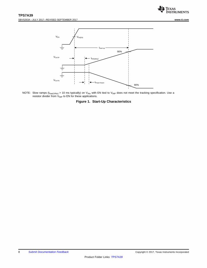
6.6 Startup Characteristicsat TJ = –40°C to +125°C, VINP(nom) = VOUTP(nom) + 1 V or VIN(nom) = 3.3 V (whichever is greater), VINN(nom) = VOUTN(nom) – 1 V orVINN(nom) = –3.3 V (whichever is less), VEN = VINP, IOUT = 1 mA, CINx = 2.2 μF, COUTx = 10 μF, CFFx = CNR/SS = 4.7nF, R1N = R2N= 10 kΩ, and FBP tied to OUTP (unless otherwise noted); typical values are at TJ = 25°C
PARAMETER TEST CONDITIONS MIN TYP MAX UNIT
tEN(delay)Delay time from EN low-to-high transition to 2.5%VOUTP
From EN low-to-high transition to VOUTP = 2.5% ×VOUTP(nom)
300 µs
tstart-upDelay time from EN low-to-high transition to bothoutputs reaching 95% of final value
From EN low-to-high transition to VOUTP =VOUTP(nom) × 95% and VOUTN = VOUTN(nom) × 95% 1.1 ms
tPstart-NstartDelay time from VOUTP leaving a high-impedancestate to VOUTN leaving a high-impedance state
From VOUTP = VOUTP(nom) × 2.5% to VOUTN =VOUTN(nom) × 2.5% –40 –17 40 µs
Δ|VOUTP –VOUTN|
Voltage difference between the positive andnegative output
During tPstart-Nstart 75 300 mV
VOUTP
VOUTN
VEN
90%
VIH(EN)
Ttstart-upt
tPstart-Nstart
90%
tEN(delay)
8
TPS7A39SBVS263A –JULY 2017–REVISED SEPTEMBER 2017 www.ti.com
Product Folder Links: TPS7A39
Submit Documentation Feedback Copyright © 2017, Texas Instruments Incorporated
NOTE: Slow ramps (trise(VINx) > 10 ms typically) on VINx with EN tied to VINP does not meet the tracking specification. Use aresistor divider from VINP to EN for these applications.
Figure 1. Start-Up Characteristics
Frequency (Hz)
Pow
er S
uppl
y R
ejec
tion
Rat
io (
dB)
0
20
40
60
80
100
10 100 1k 10k 100k 1M 10M
COUT = 4.7 PFCOUT = 10 PFCOUT = 22 PFCOUT = 47 PF
Frequency (Hz)
Pow
er S
uppl
y R
ejec
tion
Rat
io (
dB)
0
20
40
60
80
100
10 100 1k 10k 100k 1M 10M
COUT = 4.7 PFCOUT = 10 PFCOUT = 22 PFCOUT = 47 PF
Frequency (Hz)
Pow
er S
uppl
y R
ejec
tion
Rat
io (
dB)
0
20
40
60
80
100
10 100 1k 10k 100k 1M 10M
IOUT = 1 mAIOUT = 10 mAIOUT = 50 mAIOUT = 100 mAIOUT = 150 mA
Frequency (Hz)
Pow
er S
uppl
y R
ejec
tion
Rat
io (
dB)
0
20
40
60
80
100
10 100 1k 10k 100k 1M 10M
IOUT = 1 mAIOUT = 10 mAIOUT = 50 mAIOUT = 100 mAIOUT = 150 mA
Frequency (Hz)
Pow
er S
uppl
y R
ejec
tion
Rat
io (
dB)
0
20
40
60
80
100
10 100 1k 10k 100k 1M 10M
VIN = 5.5 VVIN = 5.6 VVIN = 5.7 VVIN = 5.8 VVIN = 5.9 VVIN = 6.0 V
Frequency (Hz)
Pow
er S
uppl
y R
ejec
tion
Rat
io (
dB)
0
20
40
60
80
100
10 100 1k 10k 100k 1M 10M
VINN = -5.5 VVINN = -5.6 VVINN = -5.7 V
VINN = -5.8 VVINN = -5.9 VVINN = -6.0 V
9
TPS7A39www.ti.com SBVS263A –JULY 2017–REVISED SEPTEMBER 2017
Product Folder Links: TPS7A39
Submit Documentation FeedbackCopyright © 2017, Texas Instruments Incorporated
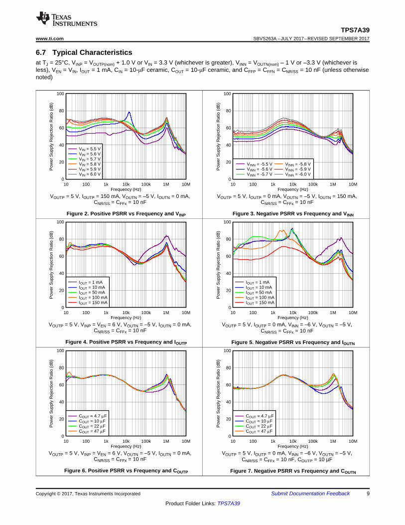
6.7 Typical Characteristicsat TJ = 25°C, VINP = VOUTP(nom) + 1.0 V or VIN = 3.3 V (whichever is greater), VINN = VOUTN(nom) – 1 V or –3.3 V (whichever isless), VEN = VIN, IOUT = 1 mA, CIN = 10-μF ceramic, COUT = 10-μF ceramic, and CFFP = CFFN = CNR/SS = 10 nF (unless otherwisenoted)
VOUTP = 5 V, IOUTP = 150 mA, VOUTN = –5 V, IOUTN = 0 mA,CNR/SS = CFFx = 10 nF
Figure 2. Positive PSRR vs Frequency and VINP
VOUTP = 5 V, IOUTP = 0 mA, VOUTN = –5 V, IOUTN = 150 mA,CNR/SS = CFFx = 10 nF
Figure 3. Negative PSRR vs Frequency and VINN
VOUTP = 5 V, VINP = VEN = 6 V, VOUTN = –5 V, IOUTN = 0 mA,CNR/SS = CFFx = 10 nF
Figure 4. Positive PSRR vs Frequency and IOUTP
VOUTP = 5 V, IOUTP = 0 mA, VINN = –6 V, VOUTN = –5 V,CNR/SS = CFFx = 10 nF
Figure 5. Negative PSRR vs Frequency and IOUTN
VOUTP = 5 V, VINP = VEN = 6 V, VOUTN = –5 V, IOUTN = 0 mA,CNR/SS = CFFx = 10 nF
Figure 6. Positive PSRR vs Frequency and COUTP
VOUTP = 5 V, IOUTP = 0 mA, VINN = –6 V, VOUTN = –5 V,CNR/SS = CFFx = 10 nF, COUTP = 10 µF
Figure 7. Negative PSRR vs Frequency and COUTN
Frequency (Hz)
Pow
er S
uppl
y R
ejec
tion
Rat
io (
dB)
0
20
40
60
80
100
10 100 1k 10k 100k 1M 10M
IOUT = 150 mA
Frequency (Hz)
Pow
er S
uppl
y R
ejec
tion
Rat
io (
dB)
0
20
40
60
80
100
10 100 1k 10k 100k 1M 10M
IOUT = 150 mA
Frequency (Hz)
Pow
er S
uppl
y R
ejec
tion
Rat
io (
dB)
0
20
40
60
80
100
10 100 1k 10k 100k 1M 10M
CNR/SS = 0 nFCNR/SS = 10 nFCNR/SS = 100 nFCNR/SS = 1000 nF
Frequency (Hz)
Pow
er S
uppl
y R
ejec
tion
Rat
io (
dB)
0
20
40
60
80
100
10 100 1k 10k 100k 1M 10M
CNR/SS = 0 nFCNR/SS = 10 nFCNR/SS = 100 nFCNR/SS = 1000 nF
Frequency (Hz)
Pow
er S
uppl
y R
ejec
tion
Rat
io (
dB)
0
20
40
60
80
100
10 100 1k 10k 100k 1M 10M
CFF = 0 nFCFF = 10 nFCFF = 100 nF
Frequency (Hz)
Pow
er S
uppl
y R
ejec
tion
Rat
io (
dB)
0
20
40
60
80
100
10 100 1k 10k 100k 1M 10M
CFFN = 0 nFCFFN = 10 nFCFFN = 100 nF
10
TPS7A39SBVS263A –JULY 2017–REVISED SEPTEMBER 2017 www.ti.com
Product Folder Links: TPS7A39
Submit Documentation Feedback Copyright © 2017, Texas Instruments Incorporated
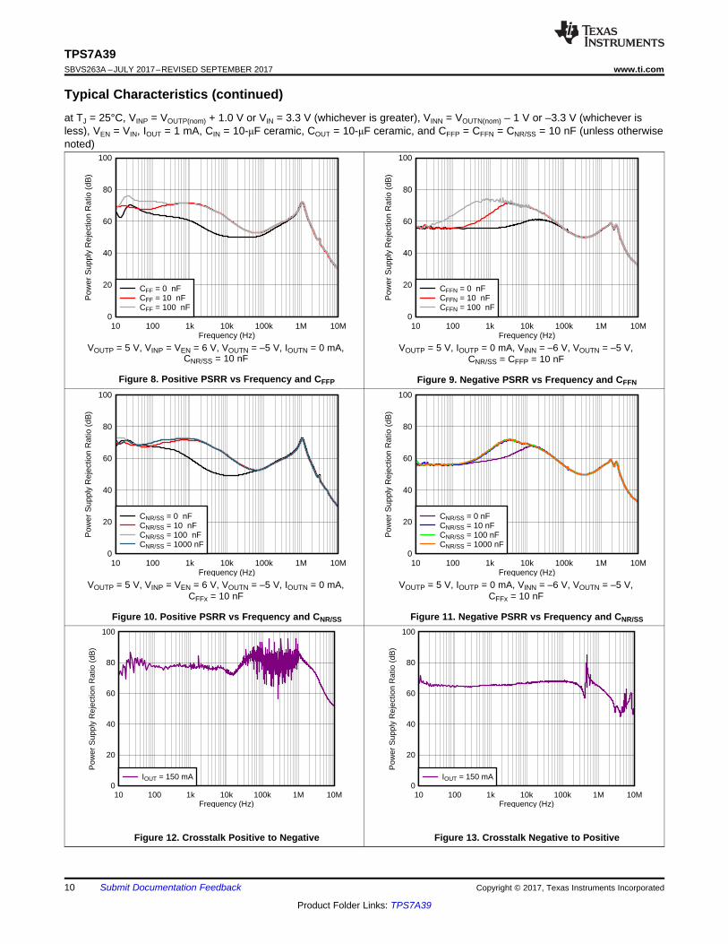
Typical Characteristics (continued)at TJ = 25°C, VINP = VOUTP(nom) + 1.0 V or VIN = 3.3 V (whichever is greater), VINN = VOUTN(nom) – 1 V or –3.3 V (whichever isless), VEN = VIN, IOUT = 1 mA, CIN = 10-μF ceramic, COUT = 10-μF ceramic, and CFFP = CFFN = CNR/SS = 10 nF (unless otherwisenoted)
VOUTP = 5 V, VINP = VEN = 6 V, VOUTN = –5 V, IOUTN = 0 mA,CNR/SS = 10 nF
Figure 8. Positive PSRR vs Frequency and CFFP
VOUTP = 5 V, IOUTP = 0 mA, VINN = –6 V, VOUTN = –5 V,CNR/SS = CFFP = 10 nF
Figure 9. Negative PSRR vs Frequency and CFFN
VOUTP = 5 V, VINP = VEN = 6 V, VOUTN = –5 V, IOUTN = 0 mA,CFFx = 10 nF
Figure 10. Positive PSRR vs Frequency and CNR/SS
VOUTP = 5 V, IOUTP = 0 mA, VINN = –6 V, VOUTN = –5 V,CFFx = 10 nF
Figure 11. Negative PSRR vs Frequency and CNR/SS
Figure 12. Crosstalk Positive to Negative Figure 13. Crosstalk Negative to Positive

Frequency (Hz)
Noi
se (P
V/
Hz)
0.001
0.002
0.005
0.01
0.02
0.05
0.1
0.2
0.5
1
2
5
10
10 100 1k 10k 100k 1M 10M
CFF0 nF, 37.77 PVRMS10 nF, 26.86 PVRMS100 nF, 22.95 PVRMS
Frequency (Hz)
Noi
se (P
V/
Hz)
0.001
0.002
0.005
0.01
0.02
0.05
0.1
0.2
0.5
1
2
5
10
10 100 1k 10k 100k 1M 10M
CFF0 nF, 45.08 PVRMS10 nF, 26.68 PVRMS100 nF, 23.53 PVRMS
Frequency (Hz)
Noi
se (P
V/
Hz)
0.001
0.002
0.005
0.01
0.02
0.05
0.1
0.2
0.5
1
2
5
10
10 100 1k 10k 100k 1M 10M
CNR/SS0 nF, 68.08 PVRMS10 nF, 26.86 PVRMS100 nF, 21.74 PVRMS1000 nF, 21.56 PVRMS
Frequency (Hz)
Noi
se (P
V/
Hz)
0.001
0.002
0.005
0.01
0.02
0.05
0.1
0.2
0.5
1
2
5
10
10 100 1k 10k 100k 1M 10M
CNR/SS0 nF, 53.32 PVRMS10 nF, 26.68 PVRMS100 nF, 23.21 PVRMS1000 nF, 23.06 PVRMS
Frequency (Hz)
Noi
se (P
V/
Hz)
0.001
0.002
0.005
0.01
0.02
0.05
0.1
0.2
0.5
1
2
5
10
10 100 1k 10k 100k 1M 10M
VOUT1.188 V, 20.63 PVRMS5 V, 26.86 PVRMS15 V, 63.88 PVRMS
Frequency (Hz)
Noi
se (P
V/
Hz)
0.001
0.002
0.005
0.01
0.02
0.05
0.1
0.2
0.5
1
2
5
10
10 100 1k 10k 100k 1M 10M
VOUT-1.188 V, 22.13 PVRMS-5 V, 28.68 PVRMS-15 V, 47.10 PVRMS
11
TPS7A39www.ti.com SBVS263A –JULY 2017–REVISED SEPTEMBER 2017
Product Folder Links: TPS7A39
Submit Documentation FeedbackCopyright © 2017, Texas Instruments Incorporated
Typical Characteristics (continued)at TJ = 25°C, VINP = VOUTP(nom) + 1.0 V or VIN = 3.3 V (whichever is greater), VINN = VOUTN(nom) – 1 V or –3.3 V (whichever isless), VEN = VIN, IOUT = 1 mA, CIN = 10-μF ceramic, COUT = 10-μF ceramic, and CFFP = CFFN = CNR/SS = 10 nF (unless otherwisenoted)
IOUTP = 150 mA, VINP = VEN, VOUTN = –VOUTP, IOUTN = 0 mA,CNR/SS = CFFx = 10 nF
Figure 14. Positive Spectral Noise Density vs Frequencyand VOUTP
IOUTN = –150 mA, VINP = VEN, VOUTN = –VOUTP, IOUTP = 0 mA,CNR/SS = CFFx = 10 nF
Figure 15. Negative Spectral Noise Density vs Frequencyand VOUTN
VOUTP = 5 V, IOUTP = 150 mA, VINP = VEN = 6 V, VOUTN = –5 V,IOUTN = 0 mA, CFFx = 10 nF
Figure 16. Positive Spectral Noise Density vs Frequencyand CNR/SS
VOUTN = –5 V, IOUTN = –150 mA, VINP = VEN = 6 V, VOUTN = –5 V,IOUTP = 0 mA, CFFx = 10 nF
Figure 17. Negative Spectral Noise Density vs Frequencyand CNR/SS
VOUTP = 5 V, IOUTP = 150 mA, VINP = VEN = 6 V, VOUTN = –5 V,IOUTN = 0 mA, CNR/SS = 10 nF
Figure 18. Positive Spectral Noise Density vs Frequencyand CFF
VOUTN = –5 V, IOUTN = –150 mA, VINP = VEN = 6 V, VOUTN = –5 V,IOUTP = 0 mA, CNR/SS = 10 nF
Figure 19. Negative Spectral Noise Density vs Frequencyand CFF

Time (ms)
Vol
tage
(V
)
0 20 40 60 80 100 120 140 160 180 200-20
-16
-12
-8
-4
0
4
8
12
16
20VINP VINN VOUTP VOUTN
Time (ms)
Vol
tage
(V
)
0 20 40 60 80 100 120 140 160 180 200-25
-20
-15
-10
-5
0
5
10
15
20
25EN VINP VOUTP VOUTN VINN
Frequency (Hz)
Noi
se (P
V/
Hz)
0.001
0.002
0.005
0.01
0.02
0.05
0.1
0.2
0.5
1
2
5
10
10 100 1k 10k 100k 1M 10M
IOUT1 mA, 29.88 PVRMS10 mA, 27.07 PVRMS50 mA, 26.66 PVRMS100 mA, 26.77 PVRMS150 mA, 26.86 PVRMS
Frequency (Hz)
Noi
se (P
V/
Hz)
0.001
0.002
0.005
0.01
0.02
0.05
0.1
0.2
0.5
1
2
5
10
10 100 1k 10k 100k 1M 10M
IOUT1 mA, 29.72 PVRMS10 mA, 28.42 PVRMS50 mA, 28.59 PVRMS100 mA, 28.47 PVRMS150 mA, 26.68 PVRMS
Frequency (Hz)
Noi
se (P
V/
Hz)
0.001
0.002
0.005
0.01
0.02
0.05
0.1
0.2
0.5
1
2
5
10
10 100 1k 10k 100k 1M 10M
COUT4.7 PF, 27.33 PVRMS10 PF, 26.86 PVRMS22 PF, 27.47 PVRMS47 PF, 27.64 PVRMS
Frequency (Hz)
Noi
se (P
V/
Hz)
0.001
0.002
0.005
0.01
0.02
0.05
0.1
0.2
0.5
1
2
5
10
10 100 1k 10k 100k 1M 10M
COUT4.7 PF, 28.43 PVRMS10 PF, 26.68 PVRMS22 PF, 26.67 PVRMS47 PF, 28.70 PVRMS
12
TPS7A39SBVS263A –JULY 2017–REVISED SEPTEMBER 2017 www.ti.com
Product Folder Links: TPS7A39
Submit Documentation Feedback Copyright © 2017, Texas Instruments Incorporated
Typical Characteristics (continued)at TJ = 25°C, VINP = VOUTP(nom) + 1.0 V or VIN = 3.3 V (whichever is greater), VINN = VOUTN(nom) – 1 V or –3.3 V (whichever isless), VEN = VIN, IOUT = 1 mA, CIN = 10-μF ceramic, COUT = 10-μF ceramic, and CFFP = CFFN = CNR/SS = 10 nF (unless otherwisenoted)
VOUTP = 5 V, IOUTP = 150 mA, VINP = VEN = 6 V, VOUTN = –5 V,IOUTN = 0 mA, CNR/SS = CFFx = 10 nF
Figure 20. Positive Spectral Noise Density vs Frequencyand COUT
VOUTN = –5 V, IOUTN = –150 mA, VINP = VEN = 6 V, VOUTN = –5 V,IOUTP = 0 mA, CNR/SS = CFFx = 10 nF
Figure 21. Negative Spectral Noise Density vs Frequencyand COUT
VOUTP = 5 V, VINP = VEN = 6 V, VOUTN = –5 V, IOUTN = 0 mA,CNR/SS = CFFx = 10 nF
Figure 22. Positive Spectral Noise Density vs Frequencyand IOUT
VOUTN = –5 V, VINP = VEN = 6 V, VOUTN = –5 V, IOUTP = 0 mA,CNR/SS = CFFx = 10 nF
Figure 23. Negative Spectral Noise Density vs Frequencyand IOUT
VOUTP = –VOUTN = 5 V, VINP = –VINN = 12 V
Figure 24. Startup (VINP = VEN)
VOUTP = –VOUTN = 5 V, VINP = –VINN = 15 V
Figure 25. Startup With EN
Time (Ps)
Out
put V
olta
ge (
V)
Out
put C
urre
nt (
A)
0 20 40 60 80 100 120 140 160 180 2005 0
5.025 0.05
5.05 0.1
5.075 0.15
5.1 0.2VOUTPIOUTP
Time (Ps)
Out
put V
olta
ge (
V)
Out
put C
urre
nt (
A)
0 20 40 60 80 100 120 140 160 180 200-5.1 -0.2
-5.075 -0.175
-5.05 -0.15
-5.025 -0.125
-5 -0.1
-4.975 -0.075
-4.95 -0.05
-4.925 -0.025
-4.9 0VOUTPIOUTP
Time (Ps)
Inpu
t Vol
tage
(V
)
Out
put V
olta
ge (
V)
0 20 40 60 80 1004 4.8
5 4.85
6 4.9
7 4.95
8 5
9 5.05
10 5.1
11 5.15
12 5.2VINPVOUTP
Time (Ps)
Inpu
t Vol
tage
(V
)
Out
put V
olta
ge (
V)
0 20 40 60 80 100 120 140 160 180 200-12 -5.1
-11 -5.075
-10 -5.05
-9 -5.025
-8 -5
-7 -4.975
-6 -4.95
-5 -4.925
-4 -4.9
VINNVOUTN
Time (Ps)
Inpu
t Vol
tage
(V
)
Out
put V
olta
ge (
V)
0 20 40 60 80 1004 5.025
5 5.03
6 5.035
7 5.04
8 5.045
9 5.05
10 5.055
11 5.06
12 5.065VINPVOUTP
Time (Ps)
Inpu
t Vol
tage
(V
)
Out
put V
olta
ge (
V)
0 20 40 60 80 100 120 140 160 180 200-12 -5.1
-11 -5.075
-10 -5.05
-9 -5.025
-8 -5
-7 -4.975
-6 -4.95
-5 -4.925
-4 -4.9
VINNVOUTN
13
TPS7A39www.ti.com SBVS263A –JULY 2017–REVISED SEPTEMBER 2017
Product Folder Links: TPS7A39
Submit Documentation FeedbackCopyright © 2017, Texas Instruments Incorporated
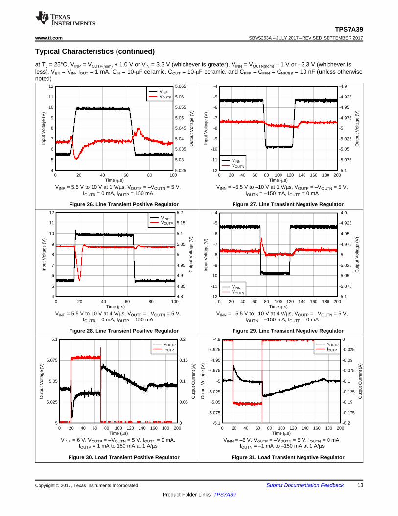
Typical Characteristics (continued)at TJ = 25°C, VINP = VOUTP(nom) + 1.0 V or VIN = 3.3 V (whichever is greater), VINN = VOUTN(nom) – 1 V or –3.3 V (whichever isless), VEN = VIN, IOUT = 1 mA, CIN = 10-μF ceramic, COUT = 10-μF ceramic, and CFFP = CFFN = CNR/SS = 10 nF (unless otherwisenoted)
VINP = 5.5 V to 10 V at 1 V/µs, VOUTP = –VOUTN = 5 V,IOUTN = 0 mA, IOUTP = 150 mA
Figure 26. Line Transient Positive Regulator
VINN = –5.5 V to –10 V at 1 V/µs, VOUTP = –VOUTN = 5 V,IOUTN = –150 mA, IOUTP = 0 mA
Figure 27. Line Transient Negative Regulator
VINP = 5.5 V to 10 V at 4 V/µs, VOUTP = –VOUTN = 5 V,IOUTN = 0 mA, IOUTP = 150 mA
Figure 28. Line Transient Positive Regulator
VINN = –5.5 V to –10 V at 4 V/µs, VOUTP = –VOUTN = 5 V,IOUTN = –150 mA, IOUTP = 0 mA
Figure 29. Line Transient Negative Regulator
VINP = 6 V, VOUTP = –VOUTN = 5 V, IOUTN = 0 mA,IOUTP = 1 mA to 150 mA at 1 A/µs
Figure 30. Load Transient Positive Regulator
VINN = –6 V, VOUTP = –VOUTN = 5 V, IOUTN = 0 mA,IOUTN = –1 mA to –150 mA at 1 A/µs
Figure 31. Load Transient Negative Regulator

Input Voltage (V)
Acc
urac
y (%
)
-33 -31 -29 -27 -25 -23-2
-1.5
-1
-0.5
0
0.5
1
1.5
2-40qC0qC25qC85qC125qC
Output Current (mA)
Acc
urac
y (%
)
0 30 60 90 120 150-2
-1.5
-1
-0.5
0
0.5
1
1.5
2-40qC0qC25qC
85qC125qC
Input Voltage (V)
Acc
urac
y (%
)
-33 -30 -27 -24 -21 -18 -15-2
-1.5
-1
-0.5
0
0.5
1
1.5
2-40qC0qC25qC85qC125qC
Input Voltage (V)
Acc
urac
y (%
)
-33 -30 -27 -24 -21 -18 -15 -12 -9 -6 -3-2
-1.5
-1
-0.5
0
0.5
1
1.5
2-40qC0qC25qC85qC125qC
Input Voltage (V)
Out
put V
olta
ge (
V)
-33 -30 -27 -24 -21 -18 -15 -12 -9 -6 -30
0.0015
0.003
0.0045
0.006
0.0075-40qC0qC25qC85qC125qC
Output Current (mA)
Out
put V
olta
ge (
V)
0 15 30 45 60 75 90 105 120 135 150-0.01
-0.005
0
0.005
0.01-40qC0qC25qC85qC125qC
14
TPS7A39SBVS263A –JULY 2017–REVISED SEPTEMBER 2017 www.ti.com
Product Folder Links: TPS7A39
Submit Documentation Feedback Copyright © 2017, Texas Instruments Incorporated
Typical Characteristics (continued)at TJ = 25°C, VINP = VOUTP(nom) + 1.0 V or VIN = 3.3 V (whichever is greater), VINN = VOUTN(nom) – 1 V or –3.3 V (whichever isless), VEN = VIN, IOUT = 1 mA, CIN = 10-μF ceramic, COUT = 10-μF ceramic, and CFFP = CFFN = CNR/SS = 10 nF (unless otherwisenoted)
VOUTN = 0 V
Figure 32. Negative Line Regulation
VOUTN = 0 V, VINN = –3.3 V
Figure 33. Negative Load Regulation
VOUTN = –1.19 V
Figure 34. Negative Line Regulation
VOUTN = –15 V
Figure 35. Negative Line Regulation
VOUTN = –24 V
Figure 36. Negative Line Regulation
VOUTN = –1.2 V, VINN = –3.3 V
Figure 37. Negative Load Regulation

Output Current (mA)
Acc
urac
y (%
)
0 30 60 90 120 150-2
-1.5
-1
-0.5
0
0.5
1
1.5
2-40qC0qC25qC
85qC125qC
Input Voltage (V)
Acc
urac
y (%
)
3 6 9 12 15 18 21 24 27 30 33-1
-0.5
0
0.5
1-40qC0qC25qC85qC125qC
Output Current (mA)
Acc
urac
y (%
)
0 30 60 90 120 150-2
-1.5
-1
-0.5
0
0.5
1
1.5
2-40qC0qC25qC
85qC125qC
Output Current (mA)
Acc
urac
y (%
)
0 30 60 90 120 150-2
-1.5
-1
-0.5
0
0.5
1
1.5
2-40qC0qC25qC
85qC125qC
Output Current (mA)
Acc
urac
y (%
)
0 30 60 90 120 150-2
-1.5
-1
-0.5
0
0.5
1
1.5
2-40qC0qC25qC
85qC125qC
Output Current (mA)
Acc
urac
y (%
)
0 30 60 90 120 150-2
-1.5
-1
-0.5
0
0.5
1
1.5
2-40qC0qC25qC
85qC125qC
15
TPS7A39www.ti.com SBVS263A –JULY 2017–REVISED SEPTEMBER 2017
Product Folder Links: TPS7A39
Submit Documentation FeedbackCopyright © 2017, Texas Instruments Incorporated
Typical Characteristics (continued)at TJ = 25°C, VINP = VOUTP(nom) + 1.0 V or VIN = 3.3 V (whichever is greater), VINN = VOUTN(nom) – 1 V or –3.3 V (whichever isless), VEN = VIN, IOUT = 1 mA, CIN = 10-μF ceramic, COUT = 10-μF ceramic, and CFFP = CFFN = CNR/SS = 10 nF (unless otherwisenoted)
VOUTN = –15 V, VINN = –16 V
Figure 38. Negative Load Regulation
VOUTN = –30 V, VINN = –33 V
Figure 39. Negative Load Regulation
VOUTP = 1.188 V, VINP = 3.3 V
Figure 40. Positive Load Regulation
VOUTP = 15 V, VINP = 16 V
Figure 41. Positive Load Regulation
VOUTP = 30 V, VINP = 33 V
Figure 42. Positive Load Regulation
VOUTP = 1.188 V
Figure 43. Positive Line Regulation
Input Voltage (V)
Dro
pout
Vol
tage
(m
V)
3 6 9 12 15 18 21 24 27 30 33100
150
200
250
300
350
400
450
500
-40qC0qC
25qC85qC
125qC
Input Voltage (V)
Dro
pout
Vol
tage
(m
V)
3 6 9 12 15 18 21 24 27 30 33100
150
200
250
300
350
400
450
500
-40qC0qC
25qC85qC
125qC
Output Current (mA)
Out
put V
olta
ge (
V)
0 50 100 150 200 250 300 350 400 450 5000
0.25
0.5
0.75
1
1.25-40qC0qC25qC85qC125qC
Output Current (mA)
Out
put V
olta
ge (
V)
0 50 100 150 200 250 300 350 400 450 500-1.25
-1
-0.75
-0.5
-0.25
0-40qC0qC25qC85qC125qC
Input Voltage (V)
Acc
urac
y (%
)
15 18 21 24 27 30 33-1
-0.5
0
0.5
1-40qC0qC25qC85qC125qC
Input Voltage (V)
Acc
urac
y (%
)
23 25.5 28 30.5 33-1
-0.5
0
0.5
1-40qC0qC25qC85qC125qC
16
TPS7A39SBVS263A –JULY 2017–REVISED SEPTEMBER 2017 www.ti.com
Product Folder Links: TPS7A39
Submit Documentation Feedback Copyright © 2017, Texas Instruments Incorporated
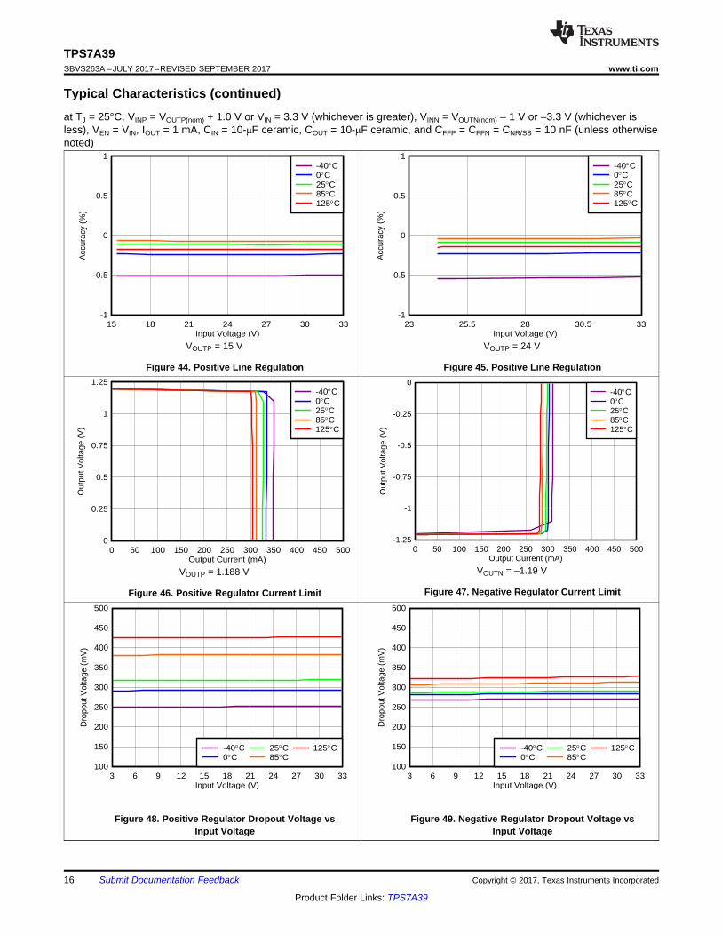
Typical Characteristics (continued)at TJ = 25°C, VINP = VOUTP(nom) + 1.0 V or VIN = 3.3 V (whichever is greater), VINN = VOUTN(nom) – 1 V or –3.3 V (whichever isless), VEN = VIN, IOUT = 1 mA, CIN = 10-μF ceramic, COUT = 10-μF ceramic, and CFFP = CFFN = CNR/SS = 10 nF (unless otherwisenoted)
VOUTP = 15 V
Figure 44. Positive Line Regulation
VOUTP = 24 V
Figure 45. Positive Line Regulation
VOUTP = 1.188 V
Figure 46. Positive Regulator Current Limit
VOUTN = –1.19 V
Figure 47. Negative Regulator Current Limit
Figure 48. Positive Regulator Dropout Voltage vsInput Voltage
Figure 49. Negative Regulator Dropout Voltage vsInput Voltage

Output Voltage (V)
Dis
char
ge C
urre
nt (
mA
)
0 5 10 15 20 25 30 350
1
2
3
4
5
6-40qC0qC
25qC85qC
125qC
Output Voltage (V)
Dis
char
ge C
urre
nt (
mA
)
-35 -30 -25 -20 -15 -10 -5 0-5
-4
-3
-2
-1
0-40qC0qC
25qC85qC
125qC
Temperature (qC)
Ena
ble
Thr
esho
ld (
V)
-50 -25 0 25 50 75 100 1251
1.25
1.5
1.75
2
Enable Falling Enable Rising
NR/SS Voltage (V)
NR
/SS
Cur
rent
(P
A)
0 0.15 0.3 0.45 0.6 0.75 0.9 1.05 1.2 1.35 1.50
2
4
6
8
10-40qC0qC25qC85qC125qC
Output Current (mA)
Dro
pout
Vol
tage
(m
V)
0 30 60 90 120 1500
50
100
150
200
250
300
350
400
450
500
550-40qC0qC25qC
85qC125qC
Output Current (mA)
Dro
pout
Vol
tage
(m
V)
0 30 60 90 120 1500
50
100
150
200
250
300
350
400
450
500
550-40qC0qC25qC
85qC125qC
17
TPS7A39www.ti.com SBVS263A –JULY 2017–REVISED SEPTEMBER 2017
Product Folder Links: TPS7A39
Submit Documentation FeedbackCopyright © 2017, Texas Instruments Incorporated
Typical Characteristics (continued)at TJ = 25°C, VINP = VOUTP(nom) + 1.0 V or VIN = 3.3 V (whichever is greater), VINN = VOUTN(nom) – 1 V or –3.3 V (whichever isless), VEN = VIN, IOUT = 1 mA, CIN = 10-μF ceramic, COUT = 10-μF ceramic, and CFFP = CFFN = CNR/SS = 10 nF (unless otherwisenoted)
VINP = 3.3 V
Figure 50. Positive Regulator Dropout Voltage vsOutput Current
VOUTN = –3.3 V
Figure 51. Negative Regulator Dropout Voltage vsOutput Current
Figure 52. Enable Threshold vs Temperature Figure 53. INR/SS vs VNR/SS
Figure 54. Positive Output Discharge Current vsOutput Voltage
Figure 55. Negative Output Discharge Current vsOutput Voltage

Output Current (mA)
Acc
urac
y (%
)
0 0.1 0.2 0.3 0.4 0.5 0.6 0.7 0.8 0.9 1-2
-1.5
-1
-0.5
0
0.5
1
1.5
2-40qC0qC25qC
85qC125qC
Output Current (mA)
Sup
ply
Cur
rent
(P
A)
0 15 30 45 60 75 90 105 120 135 150-2000
-1600
-1200
-800
-400
0-40qC0qC25qC85qC125qC
Output Current (mA)
Sup
ply
Cur
rent
(P
A)
0 30 60 90 120 1500
400
800
1200
1600
2000
-40qC0qC25qC
85qC125qC
18
TPS7A39SBVS263A –JULY 2017–REVISED SEPTEMBER 2017 www.ti.com
Product Folder Links: TPS7A39
Submit Documentation Feedback Copyright © 2017, Texas Instruments Incorporated
Typical Characteristics (continued)at TJ = 25°C, VINP = VOUTP(nom) + 1.0 V or VIN = 3.3 V (whichever is greater), VINN = VOUTN(nom) – 1 V or –3.3 V (whichever isless), VEN = VIN, IOUT = 1 mA, CIN = 10-μF ceramic, COUT = 10-μF ceramic, and CFFP = CFFN = CNR/SS = 10 nF (unless otherwisenoted)
VOUTP = 1.188 V
Figure 56. Positive Supply Current vs Output Current
VOUTN = –1.19 V
Figure 57. Negative Supply Current vs Output Current
VOUTN = –1.19 V
Figure 58. Buffer Accuracy vs Buffer Current
Positive LDO
+
±
+
±
BandgapReference
Current Limit
+±
+±
Current Limit
UVLO P
UVLO N
Negative LDO
2.6 V
- 2.6 V
INP
NR/SS
GND
INN
OUTP
FBP
FBN
OUTN
EN Internal Enable
350 k INP
BUF
UVLO N
UVLO P
x1
Thermal Shutdown
InternalEnable
InternalEnable
19
TPS7A39www.ti.com SBVS263A –JULY 2017–REVISED SEPTEMBER 2017
Product Folder Links: TPS7A39
Submit Documentation FeedbackCopyright © 2017, Texas Instruments Incorporated
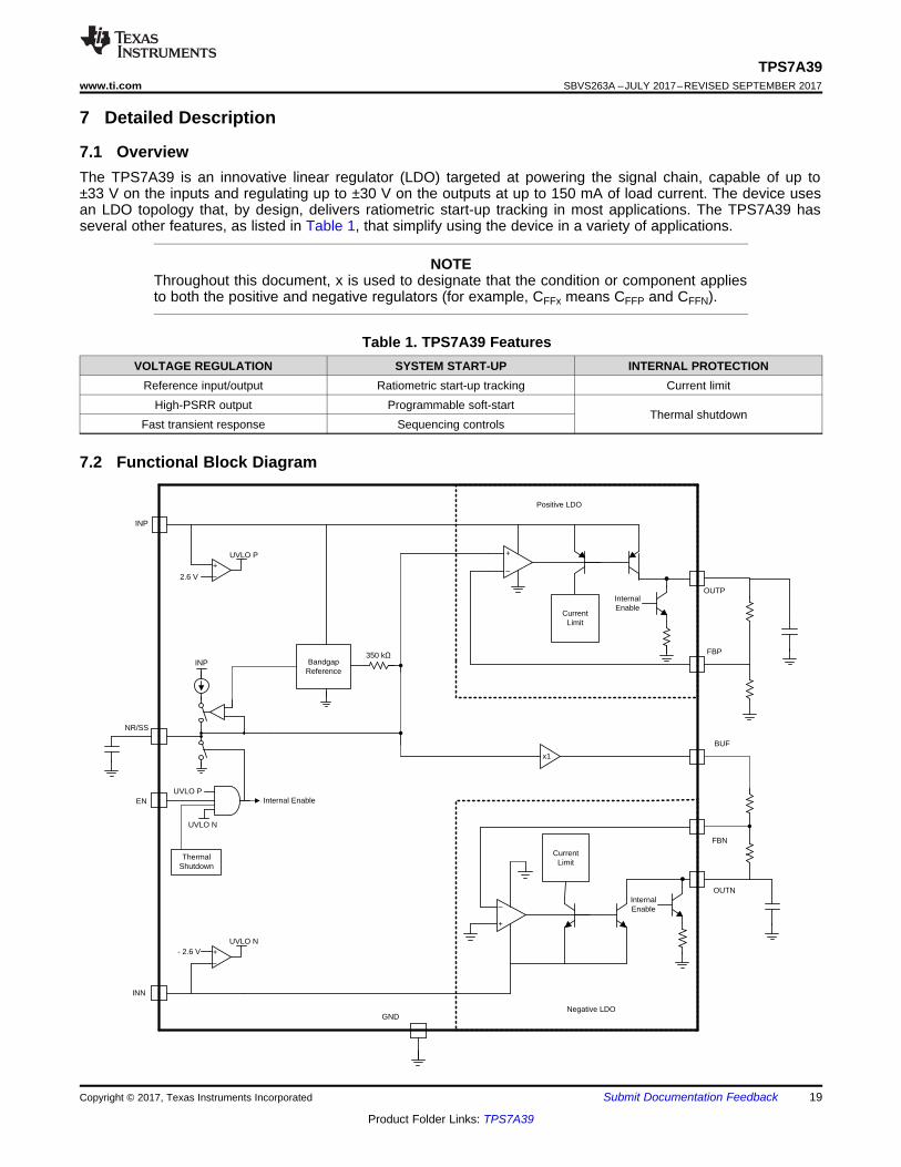
7 Detailed Description
7.1 OverviewThe TPS7A39 is an innovative linear regulator (LDO) targeted at powering the signal chain, capable of up to±33 V on the inputs and regulating up to ±30 V on the outputs at up to 150 mA of load current. The device usesan LDO topology that, by design, delivers ratiometric start-up tracking in most applications. The TPS7A39 hasseveral other features, as listed in Table 1, that simplify using the device in a variety of applications.
NOTEThroughout this document, x is used to designate that the condition or component appliesto both the positive and negative regulators (for example, CFFx means CFFP and CFFN).
Table 1. TPS7A39 FeaturesVOLTAGE REGULATION SYSTEM START-UP INTERNAL PROTECTION
Reference input/output Ratiometric start-up tracking Current limitHigh-PSRR output Programmable soft-start
Thermal shutdownFast transient response Sequencing controls
7.2 Functional Block Diagram

+ ±
VINN To Load
VBUF
VOUTN = VBUF × (-R1N/R2N)
GND
R1N
R2N
VFBN
+ ±
VINP To Load
NR/SS
VOUTP = VNR/SS × (1+R1P/R2P)
GND
R1P
R2P
VFBP
Bandgap Reference
GND
350
k CNR/SS
GND
20
TPS7A39SBVS263A –JULY 2017–REVISED SEPTEMBER 2017 www.ti.com
Product Folder Links: TPS7A39
Submit Documentation Feedback Copyright © 2017, Texas Instruments Incorporated
7.3 Feature Description
7.3.1 Voltage Regulation
7.3.1.1 DC RegulationAn LDO functions as a buffered op-amp in which the input signal is the internal reference voltage (VNR/SS), asshown in Figure 59, and in normal regulation VFBP = VNR/SS. Sharing a single reference ensures that bothchannels track each other during start-up.
VNR/SS is designed to have a very low-bandwidth at the input to the error amplifier through the use of a low-passfilter. As such, the reference can be considered as a pure dc input signal.
As Figure 60 shows, the negative LDO on the device regulates with a VFBN = 0 V and inverts the positivereference (VBUF). This topology allows the negative regulator to regulate down to 0 V.
Figure 59. Simplified Positive Regulation Circuit
Figure 60. Simplified Negative Regulation Circuit
7.3.1.2 AC and Transient ResponseEach LDO responds quickly to a transient on the input supply (line transient) or the output current (loadtransient). This LDO has a high power-supply rejection ratio (PSRR) and, when coupled with a low internal noise-floor (Vn), the LDO approximates an ideal power supply in ac and large-signal conditions.
The performance and internal layout of the device minimizes the coupling of noise from one channel to the otherchannel (crosstalk). Good printed circuit board (PCB) layout minimizes the crosstalk.
The noise-reduction and soft-start capacitor (CNR/SS) and feed-forward capacitor (CFFx) easily reduce the devicenoise floor and improve PSRR; see the Optimizing Noise and PSRR section for more information on optimizingthe noise and PSRR performance.

UVLOP
EN
UVLON
Internal Enable
10
GND
VBandgap
INR/SS
RNR/SS
CNR/SS*+
±
SW
VFBP
+
±
VBUF
GND
x1
VNR/SS
VFBN
R2N*
Note: * Denotes external components
21
TPS7A39www.ti.com SBVS263A –JULY 2017–REVISED SEPTEMBER 2017
Product Folder Links: TPS7A39
Submit Documentation FeedbackCopyright © 2017, Texas Instruments Incorporated
Feature Description (continued)7.3.2 User-Settable Buffered ReferenceAs Figure 61 shows, the device internally generated band-gap voltage outputs at the NR/SS pin. An internalresistor (RNR) and an external capacitor (CNR/SS) control the rise time of the voltage at the VNR/SS pin, setting thesoft-start time. This network also filters out noise from the band gap, reducing the overall noise floor of thedevice.
Driving the NR/SS pin with an external source can improve the device accuracy and can reduce the device noisefloor, along with enabling the device to regulate the positive channel to voltages below the device internalreference.
NOTE: * denotes external components.
Figure 61. Simplified Reference Circuit
7.3.3 Active DischargeWhen either EN or UVLOx are low, the device connects a resistance from VOUTx to GND, discharging the outputcapacitance. The active discharge circuit requires |VOUTx| ≥ 0.6 V (typ) to discharge the output because the NPNpulldown has a minimum VCE requirement.
Do not rely on the active discharge circuit for discharging large output capacitors when the input voltage dropsbelow the targeted output voltage. The TPS7A39 is a bipolar device, and as such, reverse voltage conditions(|VOUTx| ≥ |VINX| + 0.3 V) can breakdown the emitter to base diode and also cause a breakdown of the parasiticbipolar formed in the substrate; see the Reverse Current section for more details.
When either EN or UVLOx are low, the device outputs a small amount of leakage current. The leakage current istypically handled by the maximum R2x resistor value of 240 kΩ. However, if the device is placed in unity gain (noR2x resistor) this leakage current causes the output to slowly rise until the discharge circuit (as shown inFigure 62) has enough headroom to clamp the output voltage (typically ±0.6 V).
Figure 62. Simplified Active Discharge Circuit
7.3.4 System Start-Up ControlsIn many different applications, the power-supply output must turn-on within a specific window of time because ofsequencing requirements, ensuring proper operation of the load, or to minimize the loading on the input supply.
Both LDOs start-up are well-controlled and user-adjustable through the CNR/SS capacitor, solving the demandingrequirements faced by many power-supply design engineers in a simple fashion. For start-up tracking to workcorrectly. a minimum 4.7-nF CNR/SS capacitor is required. For more information on startup tracking, see theNoise-Reduction and Soft-Start Capacitor (CNR/SS) section.

UVLOP
EN
UVLON
Internal Enable
+ ±
VINP
VNR/SS
VOUTP = VNR/SS × (1+R1P/R2P)
GND
R1P
R2P
+ ±
VINN
VOUTN = VBUF × (-R1N/R2N)
GND
R1N
R2N
VBUFx1
22
TPS7A39SBVS263A –JULY 2017–REVISED SEPTEMBER 2017 www.ti.com
Product Folder Links: TPS7A39
Submit Documentation Feedback Copyright © 2017, Texas Instruments Incorporated
Feature Description (continued)
(1) The active discharge remains on as long as VINx and VOUTx provide enough headroom for the discharge circuit to function.
7.3.4.1 Start-Up TrackingFigure 63 shows how both regulators use a common reference, which enables start-up tracking. Using the samereference voltage for both the positive and negative regulators ensures that the regulators start-up together in acontrolled fashion; see Figure 24 and Figure 25.
Ramps on VINx with EN = VINP that are slower than the soft-start time do not have start-up tracking. If rampsslower than the soft-start time are used then enable should be used to start the device to ensure start-uptracking. A small mismatch between the positive and negative internal enable thresholds means that one channelturns on at a slightly lower input voltage than the other channel. This mismatch is typically not a problem in mostapplications and is easily solved by controlling the start-up with enable. The external signal can come from theinput power supply power-good indicator, a voltage supervisor output such as the TPS3701, or from anothersource.
Figure 63. Simplified Regulation Circuit
7.3.4.2 SequencingFigure 64 and Table 2 describe how the turn-on and turn-off times of both LDOs (respectively) is controlled bysetting the enable circuit (EN) and undervoltage lockout circuit (UVLOP and UVLON).
Figure 64. Simplified Turn-On Control
Table 2. Sequencing Functionality TablePOSITIVE INPUT VOLTAGE
(VINP)NEGATIVE INPUT VOLTAGE
(VINN) ENABLE STATUS LDOSTATUS
ACTIVEDISCHARGE
VINP ≥ VUVLOP VINN ≤ VUVLONEN = 1 On OffEN = 0 Off On (1)
VINP ≥ VUVLOP VINN > VUVLON EN = don't care Off On (1)
VINP < VUVLOP VINN ≤ VUVLON EN = don't care Off On (1)
VINP < VUVLOP – VHYSP VINN > VUVLON – VHYSN EN = don't care Off On (1)
23
TPS7A39www.ti.com SBVS263A –JULY 2017–REVISED SEPTEMBER 2017
Product Folder Links: TPS7A39
Submit Documentation FeedbackCopyright © 2017, Texas Instruments Incorporated
7.3.4.2.1 Enable (EN)
The enable signal (VEN) is an active-high digital control that enables the LDO when the enable voltage is past therising threshold (VEN ≥ VIH(EN)) and disables the LDO when the enable voltage is below the falling threshold (VEN≤ VIL(EN)). The exact enable threshold is between VIH(EN) and VIL(EN) because EN is a digital control. Inapplications that do not use the enable control, connect EN to VINP.
A slow VINx ramp directly connecting EN to VINP can cause the start-up tracking to move out of specification.Under slow ramp conditions, use a resistor divider from VINP to ensure start-up tracking.
7.3.4.2.2 Undervoltage Lockout (UVLO) Control
The UVLO circuit responds quickly to glitches on the input supplies and attempts to disable the output of thedevice if either of these rails collapse.
As a result of the fast response time of the input supply UVLO circuit, fast and short line transients well below theinput supply UVLO falling threshold (brownouts) can cause momentary glitches during the edges of the transient.These glitches are typical in most LDOs. The local input capacitance prevents severe brown-outs in mostapplications; see the Undervoltage Lockout (UVLOx) Control section for more details. Fast line transients cancause the outputs to momentarily shut off, and can be mitigated through using the recommended 10-µF inputcapacitor. If this becomes a problem in the system, increasing the input capacitance prevents these glitches fromoccurring.
24
TPS7A39SBVS263A –JULY 2017–REVISED SEPTEMBER 2017 www.ti.com
Product Folder Links: TPS7A39
Submit Documentation Feedback Copyright © 2017, Texas Instruments Incorporated
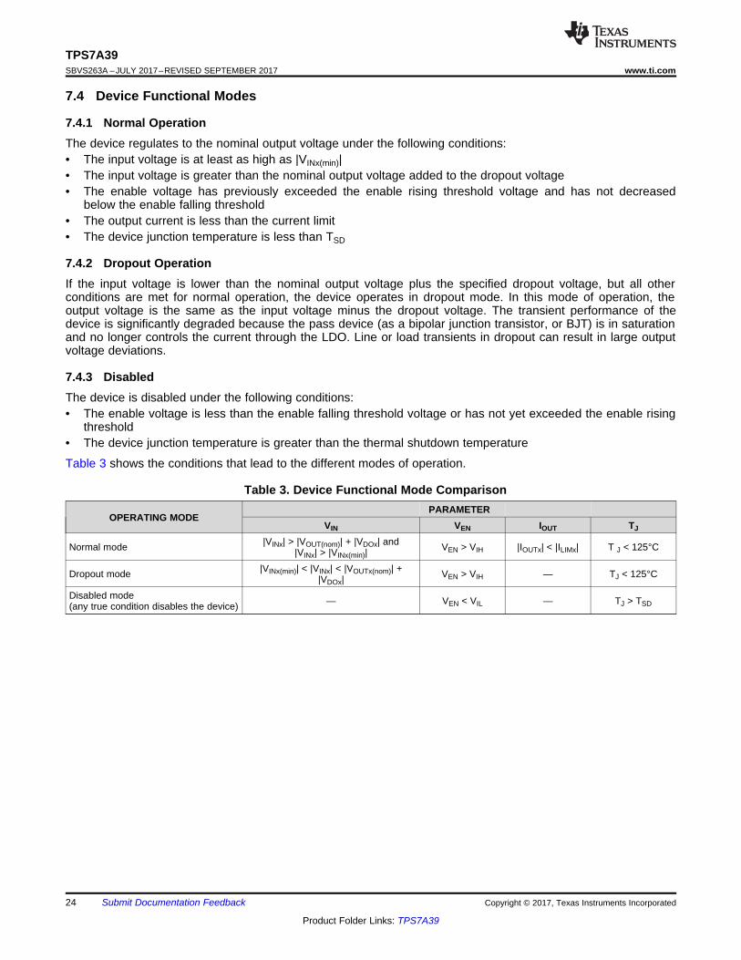
7.4 Device Functional Modes
7.4.1 Normal OperationThe device regulates to the nominal output voltage under the following conditions:• The input voltage is at least as high as |VINx(min)|• The input voltage is greater than the nominal output voltage added to the dropout voltage• The enable voltage has previously exceeded the enable rising threshold voltage and has not decreased
below the enable falling threshold• The output current is less than the current limit• The device junction temperature is less than TSD
7.4.2 Dropout OperationIf the input voltage is lower than the nominal output voltage plus the specified dropout voltage, but all otherconditions are met for normal operation, the device operates in dropout mode. In this mode of operation, theoutput voltage is the same as the input voltage minus the dropout voltage. The transient performance of thedevice is significantly degraded because the pass device (as a bipolar junction transistor, or BJT) is in saturationand no longer controls the current through the LDO. Line or load transients in dropout can result in large outputvoltage deviations.
7.4.3 DisabledThe device is disabled under the following conditions:• The enable voltage is less than the enable falling threshold voltage or has not yet exceeded the enable rising
threshold• The device junction temperature is greater than the thermal shutdown temperature
Table 3 shows the conditions that lead to the different modes of operation.
Table 3. Device Functional Mode Comparison
OPERATING MODEPARAMETER
VIN VEN IOUT TJ
Normal mode |VINx| > |VOUT(nom)| + |VDOx| and|VINx| > |VINx(min)|
VEN > VIH |IOUTx| < |ILIMx| T J < 125°C
Dropout mode |VINx(min)| < |VINx| < |VOUTx(nom)| +|VDOx|
VEN > VIH — TJ < 125°C
Disabled mode(any true condition disables the device) — VEN < VIL — TJ > TSD

INP
INN
EN
GND
NR/SS
OUTP
OUTN
BUF
FBP
FBN
TPS7A393mm x 3mm
CINP
CNR/SS
CINN
R1P
R2P
R1N
R2N
COUTN
COUTP
CFFN
CFFP
25
TPS7A39www.ti.com SBVS263A –JULY 2017–REVISED SEPTEMBER 2017
Product Folder Links: TPS7A39
Submit Documentation FeedbackCopyright © 2017, Texas Instruments Incorporated
8 Application and Implementation
NOTEInformation in the following applications sections is not part of the TI componentspecification, and TI does not warrant its accuracy or completeness. TI’s customers areresponsible for determining suitability of components for their purposes. Customers shouldvalidate and test their design implementation to confirm system functionality.
8.1 Application InformationSuccessfully implementing an LDO in an application depends on the application requirements. This sectiondiscusses key device features and how to best implement the LDO to achieve a reliable design.
8.1.1 Setting the Output Voltages on Adjustable DevicesFigure 65 shows that each LDO resistor feedback network sets its output voltage. The positive LDO outputvoltage range is VNR/SS to 30 V and the negative LDO output voltage range is 0 V to –30 V.
Figure 65. Adjustable Operation
Equation 1 relates the values of R1P and R2P to VOUTP(NOM) and VNR/SS to set the positive output voltage.Equation 2 relates the values of R1N and R2N to VOUTN(NOM) and VNR/SS to set the negative output voltage.
The positive LDO is configured as a noninverting op amp, whereas the negative LDO is an inverting op amp.VOUTP = VNR/SS × (1 + R1P / R2P) (1)VOUTN = VNR/SS × (–R1N / R2N) (2)
Substituting VNR/SS with VFBP on the positive channel and VNR/SS with VBUF on the negative channel gives a moreaccurate relationship.
Equation 3 and Equation 2 are rearranged versions of Equation 1 and Equation 2, with the above substitutionsmade.
R1P = (VOUTP / VFBP – 1) × R2P (3)R1N = –(VOUTN × R2P) / VBUF (4)
The minimum bias current through both feedback networks is 5 µA to ensure accuracy.
For even tighter accuracy, take into account the input bias current into the error amplifiers (IFBP and IFBN) and use0.1% resistors. Overriding the internal reference with a high accuracy external reference can also improve theaccuracy of the device.

26
TPS7A39SBVS263A –JULY 2017–REVISED SEPTEMBER 2017 www.ti.com
Product Folder Links: TPS7A39
Submit Documentation Feedback Copyright © 2017, Texas Instruments Incorporated
Application Information (continued)
(1) R1P is connected from OUTP to FBP, R2P is connected from FBP to GND; see the Setting the Output Voltages on Adjustable Devicessection.
Table 4 and Table 5 show the resistor combinations for several common output voltages using commerciallyavailable, 1% tolerance resistors.
Table 4. Recommended Feedback-Resistor Values for the Positive LDO
TARGETED OUTPUTVOLTAGE (V)
FEEDBACK RESISTOR VALUES (1) CALCULATED OUTPUTVOLTAGE (V)R1P (kΩ) R2P (kΩ)
1.5 2.67 10.0 1.501.8 5.23 10.0 1.802.5 11.0 10.0 2.493.0 15.4 10.0 3.003.3 17.8 10.0 3.295.0 32.4 10.0 5.029.0 66.5 10.0 9.0712.0 90.9 10.0 12.015.0 115 10.0 14.824.0 191 10.0 23.830.0 243 10.0 29.8
(1) R1N is connected from OUTN to FBN, R2N is connected from FBN to BUF; see the Setting the Output Voltages on Adjustable Devicessection.
Table 5. Recommended Feedback-Resistor Values for the Negative LDO
TARGETED OUTPUTVOLTAGE (V)
FEEDBACK RESISTOR VALUES (1) CALCULATED OUTPUTVOLTAGE (V)R1N (kΩ) R2N (kΩ)
-0.3 2.55 10.0 -0.303-1.5 12.7 10.0 -1.51-1.8 15.0 10.0 -1.78-2.5 21.0 10.0 -2.49-3.0 25.5 10.0 -3.03-3.3 28.0 10.0 -3.33-5.0 42.2 10.0 -5.04-9.0 75.0 10.0 -8.91
-12.0 100 10.0 -11.9-15.0 127 10.0 -15.1-24.0 200 10.0 -23.8-30.0 255 10.0 -30.3
8.1.2 Capacitor RecommendationsThe device is designed to be stable using low equivalent series resistance (ESR) ceramic capacitors at the inputand output pins. The device is also designed to be stable with aluminum polymer and tantalum polymercapacitors with ESR < 75 mΩ.
Electrolytic capacitors (along with higher ESR polymer capacitors) can also be used if capacitors (meeting theminimum capacitance and ESR requirements ) are used in parallel.
Take the effective ESR for stability when the impedance of the capacitor is at its minimum. At the minimum level,the capacitance and parasitic inductance cancel each other and provides the DC ESR.
Ceramic capacitors that employ X7R-, X5R-, and COG-rated dielectric materials provide relatively goodcapacitive stability across temperature, whereas the use of Y5V-rated capacitors is discouraged because of largevariations in capacitance.
27
TPS7A39www.ti.com SBVS263A –JULY 2017–REVISED SEPTEMBER 2017
Product Folder Links: TPS7A39
Submit Documentation FeedbackCopyright © 2017, Texas Instruments Incorporated
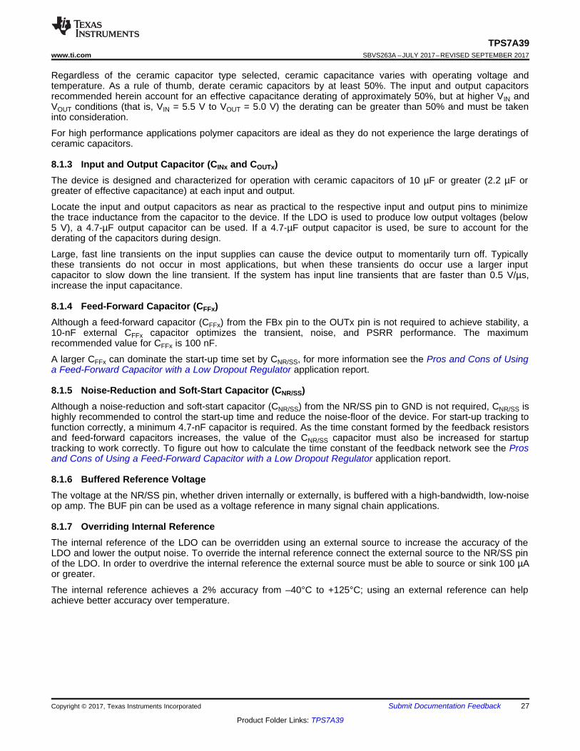
Regardless of the ceramic capacitor type selected, ceramic capacitance varies with operating voltage andtemperature. As a rule of thumb, derate ceramic capacitors by at least 50%. The input and output capacitorsrecommended herein account for an effective capacitance derating of approximately 50%, but at higher VIN andVOUT conditions (that is, VIN = 5.5 V to VOUT = 5.0 V) the derating can be greater than 50% and must be takeninto consideration.
For high performance applications polymer capacitors are ideal as they do not experience the large deratings ofceramic capacitors.
8.1.3 Input and Output Capacitor (CINx and COUTx)The device is designed and characterized for operation with ceramic capacitors of 10 µF or greater (2.2 µF orgreater of effective capacitance) at each input and output.
Locate the input and output capacitors as near as practical to the respective input and output pins to minimizethe trace inductance from the capacitor to the device. If the LDO is used to produce low output voltages (below5 V), a 4.7-µF output capacitor can be used. If a 4.7-µF output capacitor is used, be sure to account for thederating of the capacitors during design.
Large, fast line transients on the input supplies can cause the device output to momentarily turn off. Typicallythese transients do not occur in most applications, but when these transients do occur use a larger inputcapacitor to slow down the line transient. If the system has input line transients that are faster than 0.5 V/µs,increase the input capacitance.
8.1.4 Feed-Forward Capacitor (CFFx)Although a feed-forward capacitor (CFFx) from the FBx pin to the OUTx pin is not required to achieve stability, a10-nF external CFFx capacitor optimizes the transient, noise, and PSRR performance. The maximumrecommended value for CFFx is 100 nF.
A larger CFFx can dominate the start-up time set by CNR/SS, for more information see the Pros and Cons of Usinga Feed-Forward Capacitor with a Low Dropout Regulator application report.
8.1.5 Noise-Reduction and Soft-Start Capacitor (CNR/SS)Although a noise-reduction and soft-start capacitor (CNR/SS) from the NR/SS pin to GND is not required, CNR/SS ishighly recommended to control the start-up time and reduce the noise-floor of the device. For start-up tracking tofunction correctly, a minimum 4.7-nF capacitor is required. As the time constant formed by the feedback resistorsand feed-forward capacitors increases, the value of the CNR/SS capacitor must also be increased for startuptracking to work correctly. To figure out how to calculate the time constant of the feedback network see the Prosand Cons of Using a Feed-Forward Capacitor with a Low Dropout Regulator application report.
8.1.6 Buffered Reference VoltageThe voltage at the NR/SS pin, whether driven internally or externally, is buffered with a high-bandwidth, low-noiseop amp. The BUF pin can be used as a voltage reference in many signal chain applications.
8.1.7 Overriding Internal ReferenceThe internal reference of the LDO can be overridden using an external source to increase the accuracy of theLDO and lower the output noise. To override the internal reference connect the external source to the NR/SS pinof the LDO. In order to overdrive the internal reference the external source must be able to source or sink 100 µAor greater.
The internal reference achieves a 2% accuracy from –40°C to +125°C; using an external reference can helpachieve better accuracy over temperature.

C
tAt
VINx
VOUTx
UVLOx Rising Threshold
UVLOx Hysteresis
tBt tDt tEt tFt tGt
I =OUTx(t)COUTx OUTx´ dV (t)
dt
VOUTx(t)
RLOAD
+
28
TPS7A39SBVS263A –JULY 2017–REVISED SEPTEMBER 2017 www.ti.com
Product Folder Links: TPS7A39
Submit Documentation Feedback Copyright © 2017, Texas Instruments Incorporated
8.1.8 Start-Up
8.1.8.1 Soft-Start Control (NR/SS)Each output of the device features a user-adjustable, monotonic, voltage-controlled soft-start that is set with anexternal capacitor (CNR/SS). This soft-start eliminates power-up initialization problems.
The output voltage (VOUTx) rises proportionally to VNR/SS during start-up. As such, the time required for VNR/SS toreach its nominal value determines the rise time of VOUTx (start-up time).
The soft-start ramp time depends on the soft-start charging current (INR/SS), the soft-start capacitance (CNR/SS),and the internal reference (VNR/SS). Equation 5 calculates the approximate soft-start ramp time (tSS):
tSS = RNR/SS × CNR/SS × ln [(VNR/SS + INR/SS × RNR/SS) / (INR/SS×RNR/SS)] (5)
Values for the soft-start charging currents, RNR/SS, and the device internal CNR/SS are provided in the table.
8.1.8.1.1 In-Rush Current
In-rush current is defined as the current into the LDO at the INx pin during start-up. In-rush current then consistsprimarily of the sum of load current and the current used to charge the output capacitor. This current is difficult tomeasure because the input capacitor must be removed, which is not recommended. However, the in-rush currentcan be estimated by Equation 6:
where:• VOUTx(t) is the instantaneous output voltage of the turn-on ramp• dVOUTx(t) / dt is the slope of the VOUTx ramp• RLOAD is the resistive load impedance (6)
8.1.8.2 Undervoltage Lockout (UVLOx) ControlThe UVLOx circuit ensures that the device stays disabled before its input or bias supplies reach the minimumoperational voltage range, and ensures that the device properly shuts down when the input supply collapses.
Figure 66 and Table 6 explain the UVLOx circuit response to various input voltage events, assuming VEN ≥VIH(EN).
The positive and negative UVLO circuits are internally ANDed together. As such, if either supply collapses, bothoutputs turn-off and VNR/SS is pulled low internally.
Figure 66. Typical UVLOx Operation

INx10
OUTx
V (f)PSRR (dB) 20 Log
V (f )
§ · ¨ ¸
© ¹
29
TPS7A39www.ti.com SBVS263A –JULY 2017–REVISED SEPTEMBER 2017
Product Folder Links: TPS7A39
Submit Documentation FeedbackCopyright © 2017, Texas Instruments Incorporated
Table 6. Typical UVLOx Operation DescriptionREGION EVENT VOUTx STATUS COMMENT
A Turn-on, |VINx| ≤ |VUVLOx| 0 Start-upB Regulation 1 Regulates to target VOUTx
C Brownout,|VINx| ≥ |VUVLOx –VHYSx|
1 The output can fall out of regulation but the device is still enabled
D Regulation 1 Regulates to target VOUTx
E Brownout, |VINx| < |VUVLOx –VHYSx|
0
The device is disabled and the output falls because of the load andactive discharge circuit. The device is reenabled when the UVLOxrising threshold is reached by the input voltage and a normal start-up then follows.
F Regulation 1 Regulates to target VOUTx
G Turn-off, |VINx| < |VUVLOx –VHYSx|
0 The output falls because of the load and active discharge circuit
Similar to many other LDOs with this feature, the UVLOx circuit takes a few microseconds to fully assert. Duringthis time, a downward line transient below approximately 0.8 V causes the UVLOx to assert for a short time;however, the UVLOx circuit does not have enough stored energy to fully discharge the internal circuits inside ofthe device. When the UVLOx circuit is not given enough time to fully discharge the internal nodes, the outputsare not fully disabled.
The effect of the downward line transient can be mitigated by using a larger input capacitor to increase the falltime of the input supply when operating near the minimum VINx.
8.1.9 AC and Transient PerformanceLDO ac performance for a dual-channel device includes power-supply rejection ratio, channel-to-channel outputisolation, output current transient response, and output noise. These metrics are primarily a function of open-loopgain, bandwidth, and phase margin that control the closed-loop input and output impedance of the LDO. Theoutput noise is primarily a result of the band-gap reference and error amplifier noise.
8.1.9.1 Power-Supply Rejection Ratio (PSRR)PSRR is a measure of how well the LDO control-loop rejects signals from VINx to VOUTx across the frequencyspectrum (usually 10 Hz to 10 MHz). Equation 7 gives the PSRR calculation as a function of frequency for theinput signal [VINx(f)] and output signal [VOUTx(f)].
(7)
Even though PSRR is a loss in signal amplitude, PSRR is shown as positive values in decibels (dB) forconvenience.
Out
put V
olta
ge N
oise
Den
sity
(nV
/¥+])
Frequency (Hz)
Integrated NoiseFrom Bandgap and Error Amplifier
Measurement Noise Floor
1/f Noise
Wide-band Noise
Noise Gain Roll-Off
Pow
er-S
uppl
y R
ejec
tion-
Rat
io (
dB)
Frequency (Hz)
Bandgap Bandgap RC Filter
Error Amplifier, Flat-Gain Region
Error Amplifier, Gain Roll-off
Output Capacitor |ZCOUT| Decreasing
Output Capacitor |ZCOUT| Increasing
Sub 10 Hz 10 Hz ± 1 MHz100 kHz +
30
TPS7A39SBVS263A –JULY 2017–REVISED SEPTEMBER 2017 www.ti.com
Product Folder Links: TPS7A39
Submit Documentation Feedback Copyright © 2017, Texas Instruments Incorporated
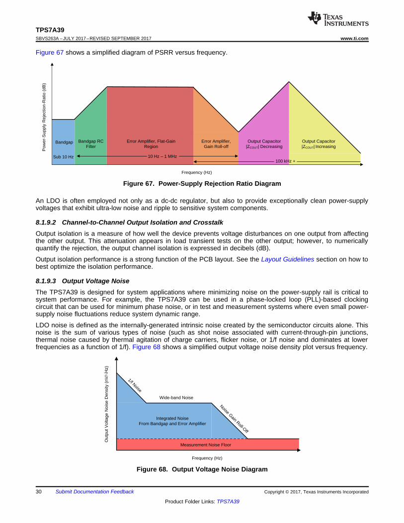
Figure 67 shows a simplified diagram of PSRR versus frequency.
Figure 67. Power-Supply Rejection Ratio Diagram
An LDO is often employed not only as a dc-dc regulator, but also to provide exceptionally clean power-supplyvoltages that exhibit ultra-low noise and ripple to sensitive system components.
8.1.9.2 Channel-to-Channel Output Isolation and CrosstalkOutput isolation is a measure of how well the device prevents voltage disturbances on one output from affectingthe other output. This attenuation appears in load transient tests on the other output; however, to numericallyquantify the rejection, the output channel isolation is expressed in decibels (dB).
Output isolation performance is a strong function of the PCB layout. See the Layout Guidelines section on how tobest optimize the isolation performance.
8.1.9.3 Output Voltage NoiseThe TPS7A39 is designed for system applications where minimizing noise on the power-supply rail is critical tosystem performance. For example, the TPS7A39 can be used in a phase-locked loop (PLL)-based clockingcircuit that can be used for minimum phase noise, or in test and measurement systems where even small power-supply noise fluctuations reduce system dynamic range.
LDO noise is defined as the internally-generated intrinsic noise created by the semiconductor circuits alone. Thisnoise is the sum of various types of noise (such as shot noise associated with current-through-pin junctions,thermal noise caused by thermal agitation of charge carriers, flicker noise, or 1/f noise and dominates at lowerfrequencies as a function of 1/f). Figure 68 shows a simplified output voltage noise density plot versus frequency.
Figure 68. Output Voltage Noise Diagram

31
TPS7A39www.ti.com SBVS263A –JULY 2017–REVISED SEPTEMBER 2017
Product Folder Links: TPS7A39
Submit Documentation FeedbackCopyright © 2017, Texas Instruments Incorporated
(1) The number of +s indicates the improvement in noise or PSRR performance by increasing the parameter value.(2) Shaded cells indicate the easiest improvement to noise or PSRR performance.
For further details, see the How to Measure LDO Noise white paper.
8.1.9.4 Optimizing Noise and PSRRTable 7 describes how the ultra-low noise floor and PSRR of the device can be improved in several ways.
Table 7. Effect of Various Parameters on AC Performance (1) (2)
PARAMETERNOISE PSRR
LOW-FREQUENCY
MID-FREQUENCY
HIGH-FREQUENCY
LOW-FREQUENCY
MID-FREQUENCY
HIGH-FREQUENCY
CNR/SS +++ No effect No effect +++ + No effectCFFx ++ +++ + ++ +++ +
COUTx No effect + +++ No effect + +++|VINx| – |VOUTx| + + + +++ +++ ++
PCB layout ++ ++ + + +++ +++
The noise-reduction capacitor, in conjunction with the noise-reduction resistor, forms a low-pass filter (LPF) thatfilters out the noise from the reference before being gained up with the error amplifier, thereby minimizing theoutput voltage noise floor. The LPF is a single-pole filter and the cutoff frequency can be calculated withEquation 8. The effect of the CNR/SS capacitor increases when VOUTx(NOM) increases because the noise from thereference is gained up when the output voltage increases. For low-noise applications, a 10-nF to 1-µF CNR/SS isrecommended.
fcutoff = 1 / (2 × π × RNR/SS × CNR/SS) (8)
The feed-forward capacitor reduces output voltage noise by filtering out the mid-band frequency noise. The feed-forward capacitor can be optimized by placing a pole-zero pair near the edge of the loop bandwidth and pushingout the loop bandwidth, thus improving mid-band PSRR.
A larger COUTx or multiple output capacitors reduces high-frequency output voltage noise and PSRR by reducingthe high-frequency output impedance of the power supply.
Additionally, a higher input voltage improves the noise and PSRR because greater headroom is provided for theinternal circuits. However, a high power dissipation across the die increases the output noise because of theincrease in junction temperature.
Good PCB layout improves the PSRR and noise performance by providing heatsinking at low frequencies andisolating VOUTx at high frequencies.
8.1.9.5 Load Transient ResponseThe load-step transient response is the output voltage response by the LDO to a step in load current, wherebyoutput voltage regulation is maintained. There are two key transitions during a load transient response: thetransition from a light to a heavy load and the transition from a heavy to a light load. The regions illustrated inFigure 69 are broken down in this section and are described in Table 8. Regions A, E, and H are where theoutput voltage is in steady-state. Increasing the output capacitance improves the transient response (less dip);however, the transient takes longer to recover when using a large output capacitor.

FB
VOUTx
IOUTx
HGECA D
32
TPS7A39SBVS263A –JULY 2017–REVISED SEPTEMBER 2017 www.ti.com
Product Folder Links: TPS7A39
Submit Documentation Feedback Copyright © 2017, Texas Instruments Incorporated
Figure 69. Load Transient Waveform
Table 8. Load Transient Waveform DescriptionREGION DESCRIPTION COMMENT
A Regulation RegulationB Output current ramping Initial voltage dip is a result of the depletion of the output capacitor charge.
C LDO responding to transient Recovery from the dip results from the LDO increasing its sourcing current, and leadsto output voltage regulation.
D Reaching thermal equilibrium At high load currents the LDO takes some time to heat up. During this time the outputvoltage changes slightly.
E Regulation Regulation
F Output current ramping Initial voltage rise results from the LDO sourcing a large current, and leads to theoutput capacitor charge to increase.
G LDO responding to transient Recovery from the rise results from the LDO decreasing its sourcing current incombination with the load discharging the output capacitor.
H Regulation Regulation
8.1.10 DC Performance
8.1.10.1 Output Voltage Accuracy (VOUTx)The device features an output voltage accuracy that includes the errors introduced by the internal reference, loadregulation, line regulation, process variation, and operating temperature as specified by the table. Output voltageaccuracy specifies minimum and maximum output voltage error, relative to the expected nominal output voltagestated as a percent (for very low output voltages this specification is in mV).
8.1.10.2 Dropout Voltage (VDO)Generally speaking, the dropout voltage often refers to the minimum voltage difference between the input andoutput voltage (|VDO| = |VINx| – |VOUTx|) that is required for regulation. When VINx drops below the required VDOxfor the given load current, the device functions as a resistive switch and does not regulate output voltage.Dropout voltage is proportional to the output current because the device is operating as a resistive switch.
8.1.11 Reverse CurrentAs with most LDOs, this device can be damaged by excessive reverse current.
Reverse current is current that flows through the substrate of the device instead of the normal conductingchannel of the pass element. This current flow, at high enough magnitudes, degrades long-term reliability of thedevice resulting from risks of electromigration and excess heat being dissipated across the device.
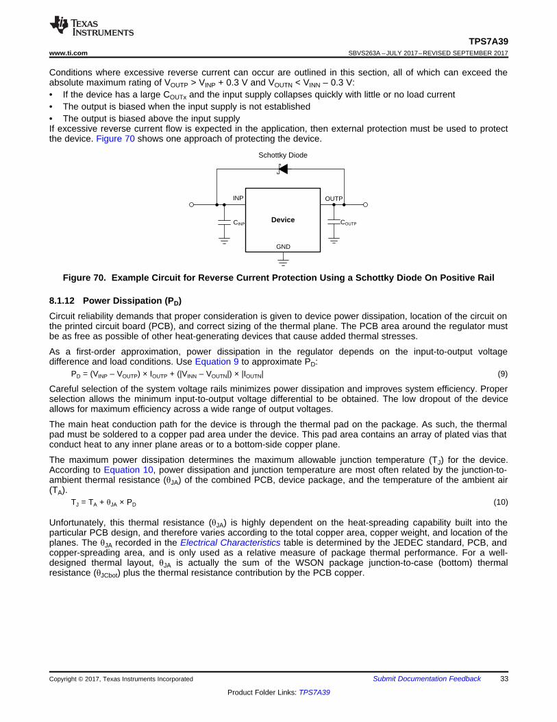
Device
INP OUTP
GND
COUTP
CINP
Schottky Diode
33
TPS7A39www.ti.com SBVS263A –JULY 2017–REVISED SEPTEMBER 2017
Product Folder Links: TPS7A39
Submit Documentation FeedbackCopyright © 2017, Texas Instruments Incorporated
Conditions where excessive reverse current can occur are outlined in this section, all of which can exceed theabsolute maximum rating of VOUTP > VINP + 0.3 V and VOUTN < VINN – 0.3 V:• If the device has a large COUTx and the input supply collapses quickly with little or no load current• The output is biased when the input supply is not established• The output is biased above the input supplyIf excessive reverse current flow is expected in the application, then external protection must be used to protectthe device. Figure 70 shows one approach of protecting the device.
Figure 70. Example Circuit for Reverse Current Protection Using a Schottky Diode On Positive Rail
8.1.12 Power Dissipation (PD)Circuit reliability demands that proper consideration is given to device power dissipation, location of the circuit onthe printed circuit board (PCB), and correct sizing of the thermal plane. The PCB area around the regulator mustbe as free as possible of other heat-generating devices that cause added thermal stresses.
As a first-order approximation, power dissipation in the regulator depends on the input-to-output voltagedifference and load conditions. Use Equation 9 to approximate PD:
PD = (VINP – VOUTP) × IOUTP + (|VINN – VOUTN|) × |IOUTN| (9)
Careful selection of the system voltage rails minimizes power dissipation and improves system efficiency. Properselection allows the minimum input-to-output voltage differential to be obtained. The low dropout of the deviceallows for maximum efficiency across a wide range of output voltages.
The main heat conduction path for the device is through the thermal pad on the package. As such, the thermalpad must be soldered to a copper pad area under the device. This pad area contains an array of plated vias thatconduct heat to any inner plane areas or to a bottom-side copper plane.
The maximum power dissipation determines the maximum allowable junction temperature (TJ) for the device.According to Equation 10, power dissipation and junction temperature are most often related by the junction-to-ambient thermal resistance (θJA) of the combined PCB, device package, and the temperature of the ambient air(TA).
TJ = TA + θJA × PD (10)
Unfortunately, this thermal resistance (θJA) is highly dependent on the heat-spreading capability built into theparticular PCB design, and therefore varies according to the total copper area, copper weight, and location of theplanes. The θJA recorded in the Electrical Characteristics table is determined by the JEDEC standard, PCB, andcopper-spreading area, and is only used as a relative measure of package thermal performance. For a well-designed thermal layout, θJA is actually the sum of the WSON package junction-to-case (bottom) thermalresistance (θJCbot) plus the thermal resistance contribution by the PCB copper.

10 F
10 F 0.1 F
0.1 F
VINP
INP
INN
EN
GND
NR/SS
OUTP
OUTN
BUF
FBP
FBN
TPS7A393mm x 3mm
COUTN
R1P
R2P
10 nF
R1N
R2N
10 nF
COUTP
10 nF
D2
D1
VCC
CLK
EN
GND
+5V
SN6505B
10 F 0.1 F
Diode1 Diode2
Diode3 Diode4
TP1
TP2
To Signal
Y
Y Y ´
JT J T JT D: T = T + PY ´
JB J B JB D: T = T + P
34
TPS7A39SBVS263A –JULY 2017–REVISED SEPTEMBER 2017 www.ti.com
Product Folder Links: TPS7A39
Submit Documentation Feedback Copyright © 2017, Texas Instruments Incorporated
(1) |IOUTN| = IOUTP = 50 mA.
8.1.12.1 Estimating Junction TemperatureThe JEDEC standard recommends the use of psi (Ψ) thermal metrics to estimate the junction temperatures ofthe LDO when in-circuit on a typical PCB board application. These metrics are not strictly speaking thermalresistances, but rather offer practical and relative means of estimating junction temperatures. These psi metricsare determined to be significantly independent of the copper-spreading area. The key thermal metrics (ΨJT andΨJB) are given in the Electrical Characteristics table and are used in accordance with Equation 11.
where:• PD is the power dissipated as explained in Equation 9• TT is the temperature at the center-top of the device package• TB is the PCB surface temperature measured 1 mm from the device package and centered on the package
edge (11)
8.2 Typical Applications
8.2.1 Design 1: Single-Ended to Differential Isolated Supply
Figure 71. Single-Ended to Differential Isolated Supply Schematic
8.2.1.1 Design Requirements
Table 9. Design RequirementsPARAMETER DESIGN REQUIREMENT DESIGN RESULTInput supply Must operate off of 5-V input 5-V input supply
Output supply Must have a 5-V and –5-V output ±5-V output, ±2% accuracyPositive output
current Capable of sourcing 50 mA on positive output 50 mA (sourcing)
Negative outputcurrent Capable of sinking 50 mA on negative output 50 mA (sinking)
Isolation from 5-Vsupply Must be isolated from input supply Isolated through center tapped transformer
Efficiency Must have > 80% efficiency at 100 mA (1) 85% efficiency when IOUTN = –50 mA and IOUTP =50 mA

n
VINVOUT+ = n·VIN
VOUT- = n·VIN
35
TPS7A39www.ti.com SBVS263A –JULY 2017–REVISED SEPTEMBER 2017
Product Folder Links: TPS7A39
Submit Documentation FeedbackCopyright © 2017, Texas Instruments Incorporated
8.2.1.2 Detailed Design Procedure
8.2.1.2.1 Switcher Choice
This design incorporates a push-pull driver for center-tapped transformers that takes a single-ended supply andconverts the supply to an isolated split rail design. The SN6505B provides a simple small-form factor isolatedsupply. The input voltage of the SN6505B can vary from 2.25 V to 5 V, which allows for use with a wide range ofinput supplies. The output voltage can be adjusted through the turns ratio of the transformer. Based on thechoice of the transformer this design can be used to create output voltages from ±3.3 V to ±15 V. In this designthe SN6505B was paired with the 750315371 center-tapped transformer from Wurth Electronics™. Thistransformer has a turns ratio of 1:1.1 and an isolation rating of 2500 VRMS (the total system isolation was nevertested).
8.2.1.2.2 Full Bridge Rectifier With Center-Tapped Transformer
To create the isolated supply, the SN6505B uses a center-tapped transformer. A full bridge rectifier andcapacitors are required to regulate the signal before reaching the LDO because of the alternating nature of theinput signal. TI recommends having a fast switching and low forward voltage diode to improve efficiency becauseof how fast the SN6505 switches; Schottky diodes work well. Figure 73 shows the switching nodes of theSN6505 D1 and D2 and also shows where the transformer connects to the full bridge rectifier TP1 and TP2.Figure 73 shows the switching waveforms across the rectifier diodes.
Figure 72. Bridge Rectifier With Center-Tapped Secondary Enables Bipolar Outputs
8.2.1.2.3 Total Solution Efficiency
Equation 12 shows how the efficiency of the system can be measured by taking the output power and dividing bythe input power. IOUTP = |IOUTN| = IOUT / 2 because this system has two output rails to simplify the efficiencymeasurement. When the necessary parameters are measured, and by using Equation 12, the overall systemefficiency can be plotted as in Figure 74. Figure 74 shows the overall system efficiency for this design, at themaximum output current of 100 mA (IOUTP = 50 mA, IOUTN = –50 mA) the efficiency of the system is 85%.
η = (IOUTP × VOUTP + IOUTN × VOUTN) / (IIN × VIN) (12)
8.2.1.2.4 Feedback Resistor Selection
Equation 13 and Equation 14 calculate the values of the feedback resistors.VOUTP = VFBP × (1 + R1P / R2P) (13)VOUTN = VBUF × (–R1N / R2N) (14)
For this design the recommended 10-kΩ resistors are used for R2P and R2N. R1P and R1N can be calculated bysubstituting R2P and R2N into Equation 15 and Equation 16 because R2P and R2N are already selected
R1P = [(VOUTP / VFBP) – 1] × R2P = [(5 V / 1.188 V) – 1] × 10 kΩ = 32.2 kΩ (15)R1N = –VOUTN × R2N / VBUF = –(–5 V) × 10 kΩ / 1.19 V = 42 kΩ (16)
After solving for Equation 15 and Equation 16, the closest one percent resistors are selected, R1N = 42.2 kΩ andR1P = 32.4 kΩ.

Frequency (Hz)
Noi
se (P
V/
Hz)
0.001
0.002
0.005
0.01
0.02
0.05
0.1
0.2
0.5
1
2
5
10
10 100 1k 10k 100k 1M 10M
IOUT = 50 mA
Time (ms)
Vol
tage
(V
)
0 10 20 30 40 50 60 70 80 90 100-10
-8
-6
-4
-2
0
2
4
6
8
10VCC VINP VOUTP VINN VOUTN
Frequency (Hz)
Noi
se (P
V/
Hz)
0.001
0.002
0.005
0.01
0.02
0.05
0.1
0.2
0.5
1
2
5
10
10 100 1k 10k 100k 1M 10M
IOUT = 50 mA
IOUT (mA)
Effi
cien
cy (
%)
0 10 20 30 40 50 60 70 80 90 1000
10
20
30
40
50
60
70
80
90
100
Time (Ps)
Vol
tage
(V
)
0 5 10 15 20 25 30 35 40 45 50-20
-16
-12
-8
-4
0
4
8
12
16
20D1 D2 TP1 TP2
36
TPS7A39SBVS263A –JULY 2017–REVISED SEPTEMBER 2017 www.ti.com
Product Folder Links: TPS7A39
Submit Documentation Feedback Copyright © 2017, Texas Instruments Incorporated
8.2.1.3 Application Curves
Figure 73. Switching Node of the SN6505B
IOUT = IOUTP + |IOUTN|, IOUTP = |IOUTN|
Figure 74. Efficiency vs Output Current
Figure 75. System Startup Figure 76. OUTP Noise
Figure 77. OUTN Noise
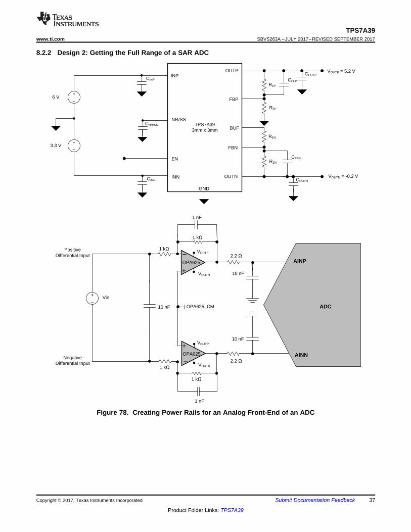
ADC
AINP
AINNOPA625
+
±
OPA625
±
+
1 k
1 k
1 nF
10 nF
1 k 2.2
2.2
10 nF
10 nF
OPA625_CM
1 k
1 nF
VOUTP
VOUTN
VOUTP
VOUTN
INP
INN
EN
GND
NR/SS
OUTP
OUTN
BUF
FBP
FBN
TPS7A393mm x 3mm
CINP
CNR/SS
CINN
R1P
R2P
R2N
R1N
COUTN
COUTP
CFFN
CFFP
+
±
+
±3.3 V
6 V
VOUTP = 5.2 V
VOUTN = -0.2 V
Positive Differential Input
Negative Differential Input
+
±
Vin
37
TPS7A39www.ti.com SBVS263A –JULY 2017–REVISED SEPTEMBER 2017
Product Folder Links: TPS7A39
Submit Documentation FeedbackCopyright © 2017, Texas Instruments Incorporated
8.2.2 Design 2: Getting the Full Range of a SAR ADC
Figure 78. Creating Power Rails for an Analog Front-End of an ADC
38
TPS7A39SBVS263A –JULY 2017–REVISED SEPTEMBER 2017 www.ti.com
Product Folder Links: TPS7A39
Submit Documentation Feedback Copyright © 2017, Texas Instruments Incorporated
8.2.2.1 Design RequirementsA common problem in analog-to-digital converters (ADCs) is that as the input signal approaches the edge of therange of the ADC, the signal begins to become distorted. Often times this is not because of a limitation of theADC, but is a result of the analog front-end (AFE). In the AFE, the signal begins to approach the rails of the opamp and the signal begins to lose linearity and becomes distorted. This distortion is because when the rail-to-railop amp begins to enter the nonlinear region of operation within 100 mV of the rail, the signal-to-noise ratio (SNR)starts to degrade and the total harmonic distortion (THD) of the ADC increases. To prevent the op amp fromexiting the linear region of operation, the design must use a power supply that can generate rails 200 mV aboveand below the input range of the ADC.
8.2.2.2 Detailed Design ProcedureIn this design, the ADS8900B is used as the ADC. This ADC features a differential input, so from a 5-V referencethe ADC is able to encode values between ±5 V. In many applications, single-supply op amps are powered withrails from 0 V to 5 V, which causes the input signal to become distorted when the full range signal is applied. TheFFT of a 10-VPP (peak-to-peak) sine wave using a single 5-V rail to bias the amplifiers is illustrated in Figure 79.In this test the SNR was calculated to be 54.89 dB and the THD was calculated to be –40.68 dB.
There is a simple solution to improve the SNR and THD of the ADC: bias the amplifiers in the analog front endwith a 5.2-V rail and a –0.2-V rail. Using these rails allows the amplifier to operate in the linear region in the 0-Vto 5-V range needed by the ADC. The FFT of a 10-VPP sine wave using a 5.2-V rail and a –0.2-V rail is illustratedin Figure 80. In this test the SNR was calculated to be 102.535 dB and the THD was calculated to be–121.66 dB. Using –0.2-V and 5.2-V rail voltages still allows for common 5-V (5.5 V max) op amps to be used inthe design.
8.2.2.3 Detailed Design Description
8.2.2.3.1 Regulation of –0.2 V
The TPS7A39 has an innovative feature of regulating the negative rail down to zero volts. This regulation isachieved by using an inverting amplifier and using the positive-buffered reference as the input signal to theamplifier. Regulating to –0.2 V eliminates the nonlinearity and distortion present when using the full rail range ofthe amplifiers.
8.2.2.3.2 Feedback Resistor Selection
Use Equation 17 and Equation 18 to calculate the values of the feedback resistors:VOUTP = VFBP × (1 + R1P / R2P) (17)VOUTN = VBUF × (–R1N / R2N) (18)
For this design the recommended 10-kΩ resistors are used for R2P and R2N. R1P and R1N can be calculated bysubstituting R2P and R2N into Equation 19 and Equation 20 because R2P and R2N are already selected.
R1P = [(VOUTP / VFBP) – 1] × R2P = [(5.2 V / 1.188 V) – 1] × 10 kΩ = 33.8 kΩ (19)R1N = –VOUTN × R2N / VBUF = –(–5 V) × 10 kΩ / 1.19 V = 1.68 kΩ (20)
After solving for Equation 19 and Equation 20, the closest one percent resistors are selected, R1N = 1.69 kΩ andR1P = 34 kΩ.

Frequency (Hz)
Am
plitu
de (
dBC
)
-200
-180
-160
-140
-120
-100
-80
-60
-40
-20
0
100 1k 10k 100kFrequency (Hz)
Am
plitu
de (
dBC
)
-200
-180
-160
-140
-120
-100
-80
-60
-40
-20
0
100 1k 10k 100k
39
TPS7A39www.ti.com SBVS263A –JULY 2017–REVISED SEPTEMBER 2017
Product Folder Links: TPS7A39
Submit Documentation FeedbackCopyright © 2017, Texas Instruments Incorporated
8.2.2.4 Application Curves
fIN = 1 kHz, VPP = 10.0 V
Figure 79. FFT Using 5-V and 0-V Supply Rails
fIN = 1 kHz, VPP = 10.0 V
Figure 80. FFT Using 5.2-V and –0.2-V Supply Rails
9 Power-Supply RecommendationsThe input supply for the LDO must be within the recommended operating conditions. The input voltage mustprovide adequate headroom in order for the device to have a regulated output. Place the 10-µF input capacitorsas close to the device as possible. If the input supply is noisy, additional input capacitors can help improve theoutput noise performance.
10 Layout
10.1 Layout GuidelinesLayout is a critical part of good power-supply design. There are several signal paths that conduct fast-changingcurrents or voltages that can interact with stray inductance or parasitic capacitance to generate noise or degradethe power-supply performance. To help eliminate these problems, bypass the IN pin to ground with capacitors.
Tie the GND pin directly to the thermal pad under the device. The thermal pad must be connected to any internalPCB ground planes using multiple vias directly under the device.
Every capacitor must be placed as close as possible to the device and on the same side of the PCB as theregulator itself.
Do not place any of the capacitors on the opposite side of the PCB from where the regulator is installed. The useof vias and long traces is strongly discouraged because these circuits can impact system performancenegatively, and even cause instability.
10.1.1 Board Layout Recommendations to Improve PSRR and Noise PerformanceTo improve ac performance (such as PSRR, output noise, and transient response), TI recommends that theboard be designed with separate ground planes for VIN and VOUT, with each ground plane star connected only atthe GND pin of the device. In addition, the ground connection for the bypass capacitor must connect directly tothe GND pin of the device.

The
rmal
Pad
INP
EN
NR
/S
SG
ND
INN
OU
TN
FB
NB
UF
FB
PO
UT
P
40
TPS7A39SBVS263A –JULY 2017–REVISED SEPTEMBER 2017 www.ti.com
Product Folder Links: TPS7A39
Submit Documentation Feedback Copyright © 2017, Texas Instruments Incorporated
10.2 Layout Example
Figure 81. Layout Example for Adjustable Option
10.3 Package MountingSolder pad footprint recommendations for the TPS7A39 are available at the end of this document and atwww.ti.com.

41
TPS7A39www.ti.com SBVS263A –JULY 2017–REVISED SEPTEMBER 2017
Product Folder Links: TPS7A39
Submit Documentation FeedbackCopyright © 2017, Texas Instruments Incorporated
11 Device and Documentation Support
11.1 Device Support
11.1.1 Development Support
11.1.1.1 Evaluation ModulesAn evaluation module (EVM) is available to assist in the initial circuit performance evaluation using the TPS7A39.The TPS7A39EVM-865 evaluation module (and related user guide) can be requested at the Texas Instrumentswebsite through the product folder or purchased directly from the TI eStore.
11.1.1.2 Spice ModelsComputer simulation of circuit performance using SPICE is often useful when analyzing the performance ofanalog circuits and systems. A SPICE model for the TPS7A39 is available through the product folder under Tools& Software.
11.2 Documentation Support
11.2.1 Related DocumentationFor related documentation see the following:• TPS3701 36-V Window Comparator with Internal Reference for Over- and Undervoltage Detection• SN6505 Low-Noise 1-A Transformer Drivers for Isolated Power Supplies• ADS890xB 20-Bit, High-Speed SAR ADCs With Integrated Reference Buffer, and Enhanced Performance
Features• Pros and Cons of Using a Feedforward Capacitor with a Low-Dropout Regulator• Using New Thermal Metrics• TPS7A39EVM-865 User's Guide
11.3 Receiving Notification of Documentation UpdatesTo receive notification of documentation updates, navigate to the device product folder on ti.com. In the upperright corner, click on Alert me to register and receive a weekly digest of any product information that haschanged. For change details, review the revision history included in any revised document.
11.4 Community ResourcesThe following links connect to TI community resources. Linked contents are provided "AS IS" by the respectivecontributors. They do not constitute TI specifications and do not necessarily reflect TI's views; see TI's Terms ofUse.
TI E2E™ Online Community TI's Engineer-to-Engineer (E2E) Community. Created to foster collaborationamong engineers. At e2e.ti.com, you can ask questions, share knowledge, explore ideas and helpsolve problems with fellow engineers.
Design Support TI's Design Support Quickly find helpful E2E forums along with design support tools andcontact information for technical support.
11.5 TrademarksE2E is a trademark of Texas Instruments.Wurth Electronics is a trademark of Würth Elektronik GmbH and Co.All other trademarks are the property of their respective owners.
11.6 Electrostatic Discharge CautionThis integrated circuit can be damaged by ESD. Texas Instruments recommends that all integrated circuits be handled withappropriate precautions. Failure to observe proper handling and installation procedures can cause damage.
ESD damage can range from subtle performance degradation to complete device failure. Precision integrated circuits may be moresusceptible to damage because very small parametric changes could cause the device not to meet its published specifications.

42
TPS7A39SBVS263A –JULY 2017–REVISED SEPTEMBER 2017 www.ti.com
Product Folder Links: TPS7A39
Submit Documentation Feedback Copyright © 2017, Texas Instruments Incorporated
11.7 GlossarySLYZ022 — TI Glossary.
This glossary lists and explains terms, acronyms, and definitions.
12 Mechanical, Packaging, and Orderable InformationThe following pages include mechanical, packaging, and orderable information. This information is the mostcurrent data available for the designated devices. This data is subject to change without notice and revision ofthis document. For browser-based versions of this data sheet, refer to the left-hand navigation.

PACKAGE OPTION ADDENDUM
www.ti.com 26-Sep-2017
Addendum-Page 1
PACKAGING INFORMATION
Orderable Device Status(1)
Package Type PackageDrawing
Pins PackageQty
Eco Plan(2)
Lead/Ball Finish(6)
MSL Peak Temp(3)
Op Temp (°C) Device Marking(4/5)
Samples
TPS7A3901DSCR ACTIVE WSON DSC 10 3000 Green (RoHS& no Sb/Br)
CU NIPDAU Level-2-260C-1 YEAR -40 to 125 A3901
TPS7A3901DSCT ACTIVE WSON DSC 10 250 Green (RoHS& no Sb/Br)
CU NIPDAU Level-2-260C-1 YEAR -40 to 125 A3901
(1) The marketing status values are defined as follows:ACTIVE: Product device recommended for new designs.LIFEBUY: TI has announced that the device will be discontinued, and a lifetime-buy period is in effect.NRND: Not recommended for new designs. Device is in production to support existing customers, but TI does not recommend using this part in a new design.PREVIEW: Device has been announced but is not in production. Samples may or may not be available.OBSOLETE: TI has discontinued the production of the device.
(2) RoHS: TI defines "RoHS" to mean semiconductor products that are compliant with the current EU RoHS requirements for all 10 RoHS substances, including the requirement that RoHS substancedo not exceed 0.1% by weight in homogeneous materials. Where designed to be soldered at high temperatures, "RoHS" products are suitable for use in specified lead-free processes. TI mayreference these types of products as "Pb-Free".RoHS Exempt: TI defines "RoHS Exempt" to mean products that contain lead but are compliant with EU RoHS pursuant to a specific EU RoHS exemption.Green: TI defines "Green" to mean the content of Chlorine (Cl) and Bromine (Br) based flame retardants meet JS709B low halogen requirements of <=1000ppm threshold. Antimony trioxide basedflame retardants must also meet the <=1000ppm threshold requirement.
(3) MSL, Peak Temp. - The Moisture Sensitivity Level rating according to the JEDEC industry standard classifications, and peak solder temperature.
(4) There may be additional marking, which relates to the logo, the lot trace code information, or the environmental category on the device.
(5) Multiple Device Markings will be inside parentheses. Only one Device Marking contained in parentheses and separated by a "~" will appear on a device. If a line is indented then it is a continuationof the previous line and the two combined represent the entire Device Marking for that device.
(6) Lead/Ball Finish - Orderable Devices may have multiple material finish options. Finish options are separated by a vertical ruled line. Lead/Ball Finish values may wrap to two lines if the finishvalue exceeds the maximum column width.
Important Information and Disclaimer:The information provided on this page represents TI's knowledge and belief as of the date that it is provided. TI bases its knowledge and belief on informationprovided by third parties, and makes no representation or warranty as to the accuracy of such information. Efforts are underway to better integrate information from third parties. TI has taken andcontinues to take reasonable steps to provide representative and accurate information but may not have conducted destructive testing or chemical analysis on incoming materials and chemicals.TI and TI suppliers consider certain information to be proprietary, and thus CAS numbers and other limited information may not be available for release.
In no event shall TI's liability arising out of such information exceed the total purchase price of the TI part(s) at issue in this document sold by TI to Customer on an annual basis.

PACKAGE OPTION ADDENDUM
www.ti.com 26-Sep-2017
Addendum-Page 2

TAPE AND REEL INFORMATION
*All dimensions are nominal
Device PackageType
PackageDrawing
Pins SPQ ReelDiameter
(mm)
ReelWidth
W1 (mm)
A0(mm)
B0(mm)
K0(mm)
P1(mm)
W(mm)
Pin1Quadrant
TPS7A3901DSCR WSON DSC 10 3000 330.0 12.4 3.3 3.3 1.0 8.0 12.0 Q1
TPS7A3901DSCT WSON DSC 10 250 180.0 12.4 3.3 3.3 1.0 8.0 12.0 Q1
PACKAGE MATERIALS INFORMATION
www.ti.com 1-Oct-2017
Pack Materials-Page 1

*All dimensions are nominal
Device Package Type Package Drawing Pins SPQ Length (mm) Width (mm) Height (mm)
TPS7A3901DSCR WSON DSC 10 3000 370.0 355.0 55.0
TPS7A3901DSCT WSON DSC 10 250 195.0 200.0 45.0
PACKAGE MATERIALS INFORMATION
www.ti.com 1-Oct-2017
Pack Materials-Page 2

www.ti.com
PACKAGE OUTLINE
C
10X 0.300.18
2.4 0.1
2X2
1.65 0.1
8X 0.5
10X 0.50.3
0.050.00
0.8 MAX
A 3.12.9
B
3.12.9
(0.2) TYP4X (0.25)
2X (0.5)
WSON - 0.8 mm max heightDSC0010JPLASTIC SMALL OUTLINE - NO LEAD
4221826/C 12/2017
PIN 1 INDEX AREA
SEATING PLANE
0.08 C
1
56
10
(OPTIONAL)PIN 1 ID 0.1 C A B
0.05 C
THERMAL PADEXPOSED
SYMM
SYMM11
NOTES: 1. All linear dimensions are in millimeters. Any dimensions in parenthesis are for reference only. Dimensioning and tolerancing per ASME Y14.5M. 2. This drawing is subject to change without notice. 3. The package thermal pad must be soldered to the printed circuit board for optimal thermal and mechanical performance.
SCALE 4.000

www.ti.com
EXAMPLE BOARD LAYOUT
0.07 MINALL AROUND
10X (0.25)
(2.4)
(2.8)
8X (0.5)
(1.65)
( 0.2) VIATYP
(0.575)
(0.95)
10X (0.6)
(R0.05) TYP
(3.4)
4X (0.25)
(0.5)
WSON - 0.8 mm max heightDSC0010JPLASTIC SMALL OUTLINE - NO LEAD
4221826/C 12/2017
SYMM
1
5 6
10
LAND PATTERN EXAMPLESOLDER MASK DEFINED
EXPOSED METAL SHOWNSCALE:20X
11SYMM
METAL UNDERSOLDER MASK
SOLDER MASKOPENING
NOTES: (continued) 4. This package is designed to be soldered to a thermal pad on the board. For more information, see Texas Instruments literature number SLUA271 (www.ti.com/lit/slua271).5. Vias are optional depending on application, refer to device data sheet. If any vias are implemented, refer to their locations shown on this view. It is recommended that vias under paste be filled, plugged or tented.

www.ti.com
EXAMPLE STENCIL DESIGN
(R0.05) TYP
10X (0.25)
10X (0.6)
2X (1.5)
2X(1.06)
(2.8)
(0.63)
8X (0.5)
(0.5)
4X (0.34)
4X (0.25)
(1.53)
WSON - 0.8 mm max heightDSC0010JPLASTIC SMALL OUTLINE - NO LEAD
4221826/C 12/2017
NOTES: (continued) 6. Laser cutting apertures with trapezoidal walls and rounded corners may offer better paste release. IPC-7525 may have alternate design recommendations.
SOLDER PASTE EXAMPLEBASED ON 0.125 mm THICK STENCIL
EXPOSED PAD 11:
80% PRINTED SOLDER COVERAGE BY AREASCALE:25X
SYMM
1
56
10
EXPOSED METALTYP
11
SYMM
SOLDER MASK OPENING
METAL UNDERSOLDER MASK

IMPORTANT NOTICE
Texas Instruments Incorporated (TI) reserves the right to make corrections, enhancements, improvements and other changes to itssemiconductor products and services per JESD46, latest issue, and to discontinue any product or service per JESD48, latest issue. Buyersshould obtain the latest relevant information before placing orders and should verify that such information is current and complete.TI’s published terms of sale for semiconductor products (http://www.ti.com/sc/docs/stdterms.htm) apply to the sale of packaged integratedcircuit products that TI has qualified and released to market. Additional terms may apply to the use or sale of other types of TI products andservices.Reproduction of significant portions of TI information in TI data sheets is permissible only if reproduction is without alteration and isaccompanied by all associated warranties, conditions, limitations, and notices. TI is not responsible or liable for such reproduceddocumentation. Information of third parties may be subject to additional restrictions. Resale of TI products or services with statementsdifferent from or beyond the parameters stated by TI for that product or service voids all express and any implied warranties for theassociated TI product or service and is an unfair and deceptive business practice. TI is not responsible or liable for any such statements.Buyers and others who are developing systems that incorporate TI products (collectively, “Designers”) understand and agree that Designersremain responsible for using their independent analysis, evaluation and judgment in designing their applications and that Designers havefull and exclusive responsibility to assure the safety of Designers' applications and compliance of their applications (and of all TI productsused in or for Designers’ applications) with all applicable regulations, laws and other applicable requirements. Designer represents that, withrespect to their applications, Designer has all the necessary expertise to create and implement safeguards that (1) anticipate dangerousconsequences of failures, (2) monitor failures and their consequences, and (3) lessen the likelihood of failures that might cause harm andtake appropriate actions. Designer agrees that prior to using or distributing any applications that include TI products, Designer willthoroughly test such applications and the functionality of such TI products as used in such applications.TI’s provision of technical, application or other design advice, quality characterization, reliability data or other services or information,including, but not limited to, reference designs and materials relating to evaluation modules, (collectively, “TI Resources”) are intended toassist designers who are developing applications that incorporate TI products; by downloading, accessing or using TI Resources in anyway, Designer (individually or, if Designer is acting on behalf of a company, Designer’s company) agrees to use any particular TI Resourcesolely for this purpose and subject to the terms of this Notice.TI’s provision of TI Resources does not expand or otherwise alter TI’s applicable published warranties or warranty disclaimers for TIproducts, and no additional obligations or liabilities arise from TI providing such TI Resources. TI reserves the right to make corrections,enhancements, improvements and other changes to its TI Resources. TI has not conducted any testing other than that specificallydescribed in the published documentation for a particular TI Resource.Designer is authorized to use, copy and modify any individual TI Resource only in connection with the development of applications thatinclude the TI product(s) identified in such TI Resource. NO OTHER LICENSE, EXPRESS OR IMPLIED, BY ESTOPPEL OR OTHERWISETO ANY OTHER TI INTELLECTUAL PROPERTY RIGHT, AND NO LICENSE TO ANY TECHNOLOGY OR INTELLECTUAL PROPERTYRIGHT OF TI OR ANY THIRD PARTY IS GRANTED HEREIN, including but not limited to any patent right, copyright, mask work right, orother intellectual property right relating to any combination, machine, or process in which TI products or services are used. Informationregarding or referencing third-party products or services does not constitute a license to use such products or services, or a warranty orendorsement thereof. Use of TI Resources may require a license from a third party under the patents or other intellectual property of thethird party, or a license from TI under the patents or other intellectual property of TI.TI RESOURCES ARE PROVIDED “AS IS” AND WITH ALL FAULTS. TI DISCLAIMS ALL OTHER WARRANTIES ORREPRESENTATIONS, EXPRESS OR IMPLIED, REGARDING RESOURCES OR USE THEREOF, INCLUDING BUT NOT LIMITED TOACCURACY OR COMPLETENESS, TITLE, ANY EPIDEMIC FAILURE WARRANTY AND ANY IMPLIED WARRANTIES OFMERCHANTABILITY, FITNESS FOR A PARTICULAR PURPOSE, AND NON-INFRINGEMENT OF ANY THIRD PARTY INTELLECTUALPROPERTY RIGHTS. TI SHALL NOT BE LIABLE FOR AND SHALL NOT DEFEND OR INDEMNIFY DESIGNER AGAINST ANY CLAIM,INCLUDING BUT NOT LIMITED TO ANY INFRINGEMENT CLAIM THAT RELATES TO OR IS BASED ON ANY COMBINATION OFPRODUCTS EVEN IF DESCRIBED IN TI RESOURCES OR OTHERWISE. IN NO EVENT SHALL TI BE LIABLE FOR ANY ACTUAL,DIRECT, SPECIAL, COLLATERAL, INDIRECT, PUNITIVE, INCIDENTAL, CONSEQUENTIAL OR EXEMPLARY DAMAGES INCONNECTION WITH OR ARISING OUT OF TI RESOURCES OR USE THEREOF, AND REGARDLESS OF WHETHER TI HAS BEENADVISED OF THE POSSIBILITY OF SUCH DAMAGES.Unless TI has explicitly designated an individual product as meeting the requirements of a particular industry standard (e.g., ISO/TS 16949and ISO 26262), TI is not responsible for any failure to meet such industry standard requirements.Where TI specifically promotes products as facilitating functional safety or as compliant with industry functional safety standards, suchproducts are intended to help enable customers to design and create their own applications that meet applicable functional safety standardsand requirements. Using products in an application does not by itself establish any safety features in the application. Designers mustensure compliance with safety-related requirements and standards applicable to their applications. Designer may not use any TI products inlife-critical medical equipment unless authorized officers of the parties have executed a special contract specifically governing such use.Life-critical medical equipment is medical equipment where failure of such equipment would cause serious bodily injury or death (e.g., lifesupport, pacemakers, defibrillators, heart pumps, neurostimulators, and implantables). Such equipment includes, without limitation, allmedical devices identified by the U.S. Food and Drug Administration as Class III devices and equivalent classifications outside the U.S.TI may expressly designate certain products as completing a particular qualification (e.g., Q100, Military Grade, or Enhanced Product).Designers agree that it has the necessary expertise to select the product with the appropriate qualification designation for their applicationsand that proper product selection is at Designers’ own risk. Designers are solely responsible for compliance with all legal and regulatoryrequirements in connection with such selection.Designer will fully indemnify TI and its representatives against any damages, costs, losses, and/or liabilities arising out of Designer’s non-compliance with the terms and provisions of this Notice.
Mailing Address: Texas Instruments, Post Office Box 655303, Dallas, Texas 75265Copyright © 2017, Texas Instruments Incorporated