Embed Size (px)
Citation preview
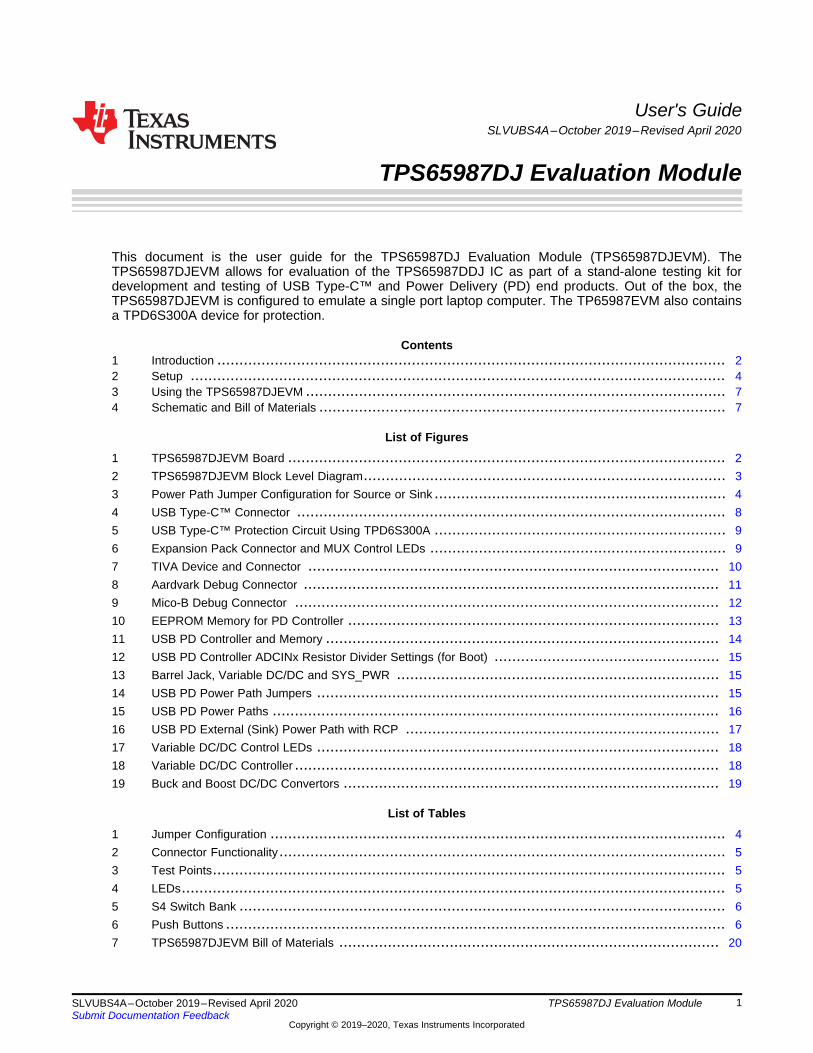
1SLVUBS4A–October 2019–Revised April 2020Submit Documentation Feedback
Copyright © 2019–2020, Texas Instruments Incorporated
TPS65987DJ Evaluation Module
User's GuideSLVUBS4A–October 2019–Revised April 2020
TPS65987DJ Evaluation Module
This document is the user guide for the TPS65987DJ Evaluation Module (TPS65987DJEVM). TheTPS65987DJEVM allows for evaluation of the TPS65987DDJ IC as part of a stand-alone testing kit fordevelopment and testing of USB Type-C™ and Power Delivery (PD) end products. Out of the box, theTPS65987DJEVM is configured to emulate a single port laptop computer. The TP65987EVM also containsa TPD6S300A device for protection.
Contents1 Introduction ................................................................................................................... 22 Setup ......................................................................................................................... 43 Using the TPS65987DJEVM ............................................................................................... 74 Schematic and Bill of Materials ............................................................................................ 7
List of Figures
1 TPS65987DJEVM Board ................................................................................................... 22 TPS65987DJEVM Block Level Diagram.................................................................................. 33 Power Path Jumper Configuration for Source or Sink .................................................................. 44 USB Type-C™ Connector ................................................................................................. 85 USB Type-C™ Protection Circuit Using TPD6S300A .................................................................. 96 Expansion Pack Connector and MUX Control LEDs ................................................................... 97 TIVA Device and Connector ............................................................................................. 108 Aardvark Debug Connector .............................................................................................. 119 Mico-B Debug Connector ................................................................................................ 1210 EEPROM Memory for PD Controller .................................................................................... 1311 USB PD Controller and Memory ......................................................................................... 1412 USB PD Controller ADCINx Resistor Divider Settings (for Boot) ................................................... 1513 Barrel Jack, Variable DC/DC and SYS_PWR ......................................................................... 1514 USB PD Power Path Jumpers ........................................................................................... 1515 USB PD Power Paths ..................................................................................................... 1616 USB PD External (Sink) Power Path with RCP ....................................................................... 1717 Variable DC/DC Control LEDs ........................................................................................... 1818 Variable DC/DC Controller ................................................................................................ 1819 Buck and Boost DC/DC Convertors ..................................................................................... 19
List of Tables
1 Jumper Configuration ....................................................................................................... 42 Connector Functionality..................................................................................................... 53 Test Points.................................................................................................................... 54 LEDs........................................................................................................................... 55 S4 Switch Bank .............................................................................................................. 66 Push Buttons ................................................................................................................. 67 TPS65987DJEVM Bill of Materials ...................................................................................... 20

Introduction www.ti.com
2 SLVUBS4A–October 2019–Revised April 2020Submit Documentation Feedback
Copyright © 2019–2020, Texas Instruments Incorporated
TPS65987DJ Evaluation Module
TrademarksUSB Type-C is a trademark of USB Implementers Forum.All other trademarks are the property of their respective owners.
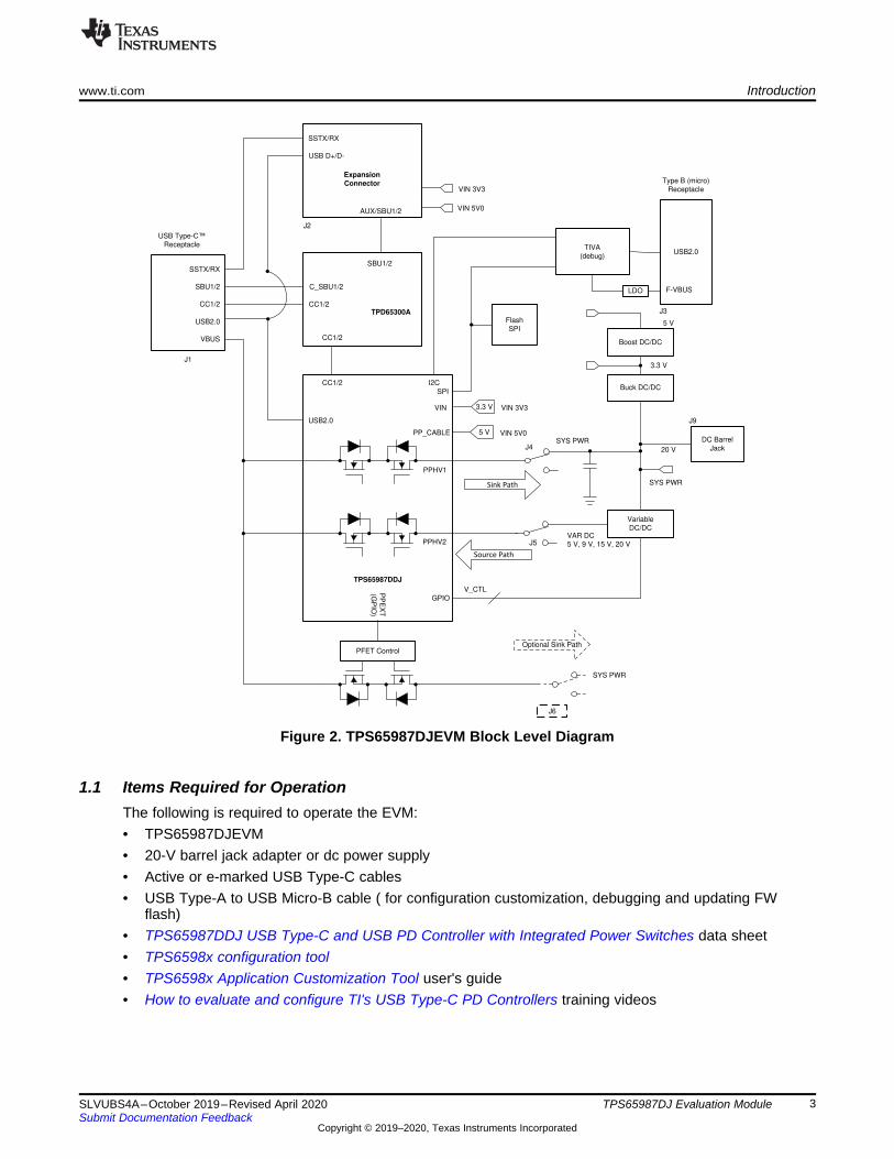
1 IntroductionTexas Instrument's (TI’s) TPS65987DJ evaluation module helps designers evaluate the operation andperformance of the TPS65987DDJ device.
The TPS65987DDJ device is a USB Type-C and Power Delivery (PD) controller providing cable plug andorientation detection at the USB Type-C connector. Upon cable detection, the TPS65987DJcommunicates on the CC wire using the USB PD protocol. When cable detection and USB PD negotiationare complete, the TPS65987DJ device enables the appropriate power path and configures Alternate Modesettings for external multiplexers. The TPS65987DDJ device has two internal power paths that can besource or sink with current rating up to 5 A. The EVM is customizable through the TPS65987DJApplication Customization Tool. Additionally, the EVM is equipped with an TIVA chip for flashing a newproject through SPI or I2C for debugging and development. The scope of this document will cover theEVM hardware. For information on how to configure the EVM, refer to the TPS6598x ApplicationCustomization Tool userguide
Figure 1 shows the TPS65987DJEVM board and Figure 2 shows a block level diagram.
Figure 1. TPS65987DJEVM Board
TPS65987DDJ
CC1/2
TPD65300A
CC1/2
CC1/2
C_SBU1/2
SBU1/2
Expansion
Connector
AUX/SBU1/2
USB D+/D-
SSTX/RX
VIN 3V3
VIN 5V0
VIN 3V3 3.3 V
VIN 5V0 5 V
Flash
SPI
Sink Path
Source Path
Variable
DC/DC
Buck DC/DC
Boost DC/DC
SYS PWR
DC Barrel
Jack
VAR DC
5 V, 9 V, 15 V, 20 V
PFET Control
SSTX/RX
SBU1/2
CC1/2
USB2.0
VBUS
USB Type-&��
Receptacle
USB2.0
TIVA
(debug)
LDO
USB2.0
Type B (micro)
Receptacle
Optional Sink Path
J6
SYS PWR
SYS PWR
V_CTL
GPIO
PPHV2
PPHV1
PP_CABLE
VIN
SPI
I2C
F-VBUS
J3
5 V
3.3 V
J9
20 V
J5
J4
J1
J2
PP
EX
T
(GP
IO)
www.ti.com Introduction
3SLVUBS4A–October 2019–Revised April 2020Submit Documentation Feedback
Copyright © 2019–2020, Texas Instruments Incorporated
TPS65987DJ Evaluation Module
Figure 2. TPS65987DJEVM Block Level Diagram
1.1 Items Required for OperationThe following is required to operate the EVM:• TPS65987DJEVM• 20-V barrel jack adapter or dc power supply• Active or e-marked USB Type-C cables• USB Type-A to USB Micro-B cable ( for configuration customization, debugging and updating FW
flash)• TPS65987DDJ USB Type-C and USB PD Controller with Integrated Power Switches data sheet• TPS6598x configuration tool• TPS6598x Application Customization Tool user's guide• How to evaluate and configure TI's USB Type-C PD Controllers training videos

SYS_PWR
PP_HV1
VAR_DCDC
1
2
3
SYS_PWR
PP_HV2
VAR_DCDC
TPS65987D
Power Paths
J5 J4
1
2
3
SYS_PWR
PP_HV2
VAR_DCDC
Jumper J6 is not used
J6
Do not populate
sink
source
sink
source
sink
source
Setup www.ti.com
4 SLVUBS4A–October 2019–Revised April 2020Submit Documentation Feedback
Copyright © 2019–2020, Texas Instruments Incorporated
TPS65987DJ Evaluation Module
2 SetupThis section describes the header and jumper connections on the EVM and getting started using theTPS65987DJEVM.
2.1 Jumper ConfigurationOut of the box, the TPS65987DJEVM is configured to use TPS65987DJ's PPHV1 as sink path (J4) andPPHV2 as source path (J5), which matches the configuration of firmware already programmed in thedevice. If you have changed FW and want to put the FW back to the way it was shipped, Recovery FWcan be reprogrammed using the Application customization tool. The recovery firmware is a full flash imagethat comes with the Application Customization tool and will configure the EVM to match the describedjumper configuration. In order to upload the recovery firmware, open the Application customization tool.Once a project has been selected, open the Device menu and select Re-Flash EVM Firmware (Recovery).
Remember, the jumper configuration in the hardware must match the source and sink paths in thesoftware, Application Customization Tool (GUI). See Figure 3 and Table 1 for the jumper configuration.
Figure 3. Power Path Jumper Configuration for Source or Sink
Table 1. Jumper Configuration
Jumper DescriptionJ4 TPS65987DDJ power path: Jump pins 1-2 to sink on PP_HV1 (default)J5 TPS65987DDJ power path: Jump pins 2-3 to source on PP_HV2 (default)

www.ti.com Setup
5SLVUBS4A–October 2019–Revised April 2020Submit Documentation Feedback
Copyright © 2019–2020, Texas Instruments Incorporated
TPS65987DJ Evaluation Module
2.2 Connector FunctionalityTable 2 lists the TPS65987DJEVM connector and functionality.
Table 2. Connector Functionality
Designator DescriptionJ1 USB Type-C connector: TI recommends using an active or e-marked USB Type-C cableJ2 Expansion board connector: Option to connect to external module.J3 Micro-B connector: Connect to a PC to flash a project on the PD controller. You must download the
TPS6598x configuration tool (GUI) to flash a project properly.J9 Barrel jack connector: Use a 19-V to 20-V DC supply. A standard Dell or HP notebook adapter (or similar) will
provide the required power.
2.3 Test PointsTable 3 lists the TPS65987DJEVM test points.
Table 3. Test Points
Test Point Label DescriptionTP1 VBUS VBUS voltage on the USB Type-C connector. Sourcing and sinking is always in
reference to VBUS (Source to VBUS or sink from VBUS).TP2 CC1 System side CC1. This could be VCONN or CC depending on polarity flip of the USB
Type-C cable.TP3 CC2 System side CC2. This could be VCONN or CC depending on polarity flip of the USB
Type-C cable.TP4, TP5, TP6 GND Ground reference for entire board
TP7 P3V3 Output of 3.3-V DC/DC convertor to power up all ICs on the EVMTP8 P5V0 Output of 5-V DC/DC convertor used for PP_CABLE (VCONN)
2.4 LEDsTable 4 lists the TPS65987DJEVM LEDs.
Table 4. LEDs
Designator Label DescriptionD12 μB VBUS White LED that shows when the μB port is connected (FTDI for GUI).D13 SSMX: DP White LED that shows when the TPS65987DDJ device has enabled this signal for the
super-speed MUX (depending on version of EVM the silkscreen may appear to showthis signal swapped with SSMX: USB3)
D14 SSMX: FLIP White LED that shows when the TPS65987DDJ device has enabled the flipped cableorientation signal for the super-speed MUX
D15 SSMX: USB3 White LED that shows when the TPS65987DDJ device has enabled this signal for thesuper-speed MUX
D16 VBUS White LED that shows when VBUS has a voltage of 5 V, 9 V, 15 V, or 20 VD19 SYS_PWR Blue LED that shows when the barrel jack is connectedD20 VAR_DCDC Green LED that shows when there is a voltage on the variable DC/DC controller (U9).
When the EVM acts as a source, D20 lights up.D21 PDO_0 White LED that shows when there is a 5-V PD contract (only shown when sourcing)D22 PDO_1 White LED that shows when there is a 9-V PD contract (only shown when sourcing)D23 PDO_2 White LED that shows when there is a 15-V PD contract (only shown when sourcing)D24 PDO_3 White LED that shows when there is a 20-V PD contract (only shown when sourcing)D17 /FLT Red LED that shows when there is an fault occurred TPD6S300A device
Setup www.ti.com
6 SLVUBS4A–October 2019–Revised April 2020Submit Documentation Feedback
Copyright © 2019–2020, Texas Instruments Incorporated
TPS65987DJ Evaluation Module
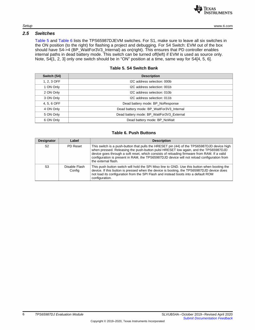
2.5 SwitchesTable 5 and Table 6 lists the TPS65987DJEVM switches. For S1, make sure to leave all six switches inthe ON position (to the right) for flashing a project and debugging. For S4 Switch: EVM out of the boxshould have S4->4 (BP_WaitFor3V3_Internal) as on(right). This ensures that PD controller enablesinternal paths in dead battery mode. This switch can be turned off(left) if EVM is used as source only.Note, S4[1, 2, 3] only one switch should be in "ON" position at a time, same way for S4[4, 5, 6].
Table 5. S4 Switch Bank
Switch (S4) Description1, 2, 3 OFF I2C address selection: 000b1 ON Only I2C address selection: 001b2 ON Only I2C address selection: 010b3 ON Only I2C address selection: 011b4, 5, 6 OFF Dead battery mode: BP_NoResponse4 ON Only Dead battery mode: BP_WaitFor3V3_Internal5 ON Only Dead battery mode: BP_WaitFor3V3_External6 ON Only Dead battery mode: BP_NoWait
Table 6. Push Buttons
Designator Label DescriptionS2 PD Reset This switch is a push-button that pulls the HRESET pin (44) of the TPS65987DJD device high
when pressed. Releasing the push-button pulsl HRESET low again, and the TPS65987DJDdevice goes through a soft reset, which consists of reloading firmware from RAM. If a validconfiguration is present in RAM, the TPS65987DJD device will not reload configuration fromthe external flash.
S3 Disable FlashConfig
This push button switch will hold the SPI Miso line to GND. Use this button when booting thedevice. If this button is pressed when the device is booting, the TPS65987DJD device doesnot load its configuration from the SPI Flash and instead boots into a default ROMconfiguration.
www.ti.com Using the TPS65987DJEVM
7SLVUBS4A–October 2019–Revised April 2020Submit Documentation Feedback
Copyright © 2019–2020, Texas Instruments Incorporated
TPS65987DJ Evaluation Module
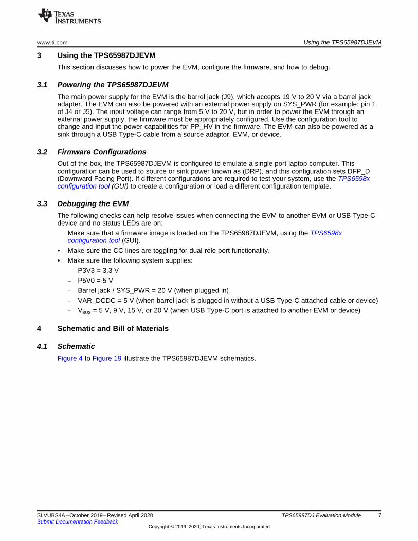
3 Using the TPS65987DJEVMThis section discusses how to power the EVM, configure the firmware, and how to debug.
3.1 Powering the TPS65987DJEVMThe main power supply for the EVM is the barrel jack (J9), which accepts 19 V to 20 V via a barrel jackadapter. The EVM can also be powered with an external power supply on SYS_PWR (for example: pin 1of J4 or J5). The input voltage can range from 5 V to 20 V, but in order to power the EVM through anexternal power supply, the firmware must be appropriately configured. Use the configuration tool tochange and input the power capabilities for PP_HV in the firmware. The EVM can also be powered as asink through a USB Type-C cable from a source adaptor, EVM, or device.
3.2 Firmware ConfigurationsOut of the box, the TPS65987DJEVM is configured to emulate a single port laptop computer. Thisconfiguration can be used to source or sink power known as (DRP), and this configuration sets DFP_D(Downward Facing Port). If different configurations are required to test your system, use the TPS6598xconfiguration tool (GUI) to create a configuration or load a different configuration template.
3.3 Debugging the EVMThe following checks can help resolve issues when connecting the EVM to another EVM or USB Type-Cdevice and no status LEDs are on:
Make sure that a firmware image is loaded on the TPS65987DJEVM, using the TPS6598xconfiguration tool (GUI).
• Make sure the CC lines are toggling for dual-role port functionality.• Make sure the following system supplies:
– P3V3 = 3.3 V– P5V0 = 5 V– Barrel jack / SYS_PWR = 20 V (when plugged in)– VAR_DCDC = 5 V (when barrel jack is plugged in without a USB Type-C attached cable or device)– VBUS = 5 V, 9 V, 15 V, or 20 V (when USB Type-C port is attached to another EVM or device)
4 Schematic and Bill of Materials
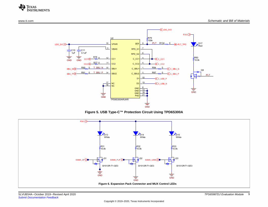
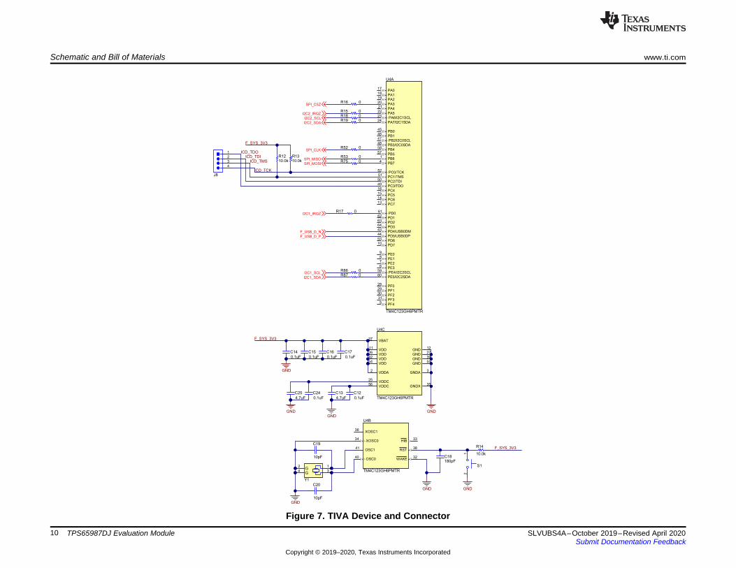
4.1 SchematicFigure 4 to Figure 19 illustrate the TPS65987DJEVM schematics.

GNDA1
SSTXp1A2
SSTXn1A3
VBUSA4
CC1A5
Dp1A6
Dn1A7
SBU1A8
VBUSA9
SSRXn2A10
SSRXp2A11
GNDB12
SSRXp1B11
SSRXn1B10
VBUSB9
SBU2B8
CC2B5
VBUSB4
SSTXn2B3
SSTXp2B2
GNDB1
GNDA12
SHIELDS1
SHIELDS2
SHIELDS3
SHIELDS4
Dp2B6
Dn2B7
J1
DX07S024JJ2R1300
TC_SSTX2_NTC_SSTX2_P
TC_SSTX1_PTC_SSTX1_N
0.01uFC2
0.01uFC3
0.01uFC4
0.01uF
C1
0 C60 C7
VBUS
C_SSTX2_N
C_SSTX2_P
GND
C_CC2
C_USB_N
C_USB_P
C_SBU_N
GND
C_SSRX1_P
C_SSRX1_N
GNDGND
C_SSRX2_N
C_SSRX2_P
GND
C_SBU_P
C_USB_P
C_USB_N
C_CC1
C_SSTX1_P
C_SSTX1_N
GND
GND
VBUS
VBUS
VBUS
0 C9
0 C8VBUS
GND
TP1
C_SBU_N
C_SBU_P DP_SBU_P
DP_SBU_N
D3D2 D5D4 D6 D7 D8 D9 D10 D11
DP_SBU_N
DP_SBU_P SBU_P
SBU_N
0R20
DNPR3
0
DNP
R40
DNP
CC1
CC2
C_CC1
C_CC20R930
DNP
R96DNP
IN4
IN5
GN
D1
GN
D2
IN6
GN
D3
PA
D7
U7
Schematic and Bill of Materials www.ti.com
8 SLVUBS4A–October 2019–Revised April 2020Submit Documentation Feedback
Copyright © 2019–2020, Texas Instruments Incorporated
TPS65987DJ Evaluation Module
Figure 4. USB Type-C™ Connector
GND
GNDGND
SSMX_USB3SSMX_FLIPSSMX_DP
P3V3
10.0kR32
10.0kR33
WhiteD14
WhiteD13
WhiteD15
10.0kR31
Q1
SI1012R-T1-GE3
Q2
SI1012R-T1-GE3
Q3
SI1012R-T1-GE3
SBU_P
SBU_N0R90
0R91
C_SBU11
C_SBU22
VBIAS3
C_CC14
C_CC25
RPD_G26
RPD_G17
GND8
FLT9
VPWR10
CC211
CC112
GND13
SBU214
SBU115
NC16
NC17
GND18
D219
D120
PAD21
TPD6S300ARUKR
U2
GND
GND
C_CC1
C_CC2
0R76
0R77
0.1uF
C11
GND
Q9
P3V3
GND
RedD17
10.0kR83
CC1
CC2
LDO_3V3
1uF
C10
GND
100kR79
LDO_3V3
/FLT
/FLT
C_USB_P
C_USB_N
C_SBU_P
0R94C_SBU_N
0R97
/FLT_TPD0R134
T_SBU_N
T_SBU_P
www.ti.com Schematic and Bill of Materials
9SLVUBS4A–October 2019–Revised April 2020Submit Documentation Feedback
Copyright © 2019–2020, Texas Instruments Incorporated
TPS65987DJ Evaluation Module
Figure 5. USB Type-C™ Protection Circuit Using TPD6S300A
Figure 6. Expansion Pack Connector and MUX Control LEDs
SPI_MOSI
SPI_MISO
SPI_CSZ
SPI_CLK
I2C2_SCL
I2C2_SDA
PB61
PB74
PF45
PE36
PE27
PE18
PE09
PD710
PC713
PC614
PC515
PC416
PA017
PA118
PA219
PA320
PA421
PA522
PA6/I2C1SCL23
PA7/I2C1SDA24
PF028
PF129
PF230
PF331
PD4/USB0DM43
PD5/USB0DP44
PB045
PB146
PB2/I2C0SCL47
PB3/I2C0SDA48
PC3/TDO49
PC2/TDI50
PC1/TMS51
PC0/TCK52
PD653
PB557
PB458
PE4/I2C2SCL59
PE5/I2C2SDA60
PD061
PD162
PD263
PD364
TM4C123GH6PMTR
U4A
ICD_TCK
ICD_TMSICD_TDI
ICD_TDO
10.0kR13
10.0kR12
0R180R19
0R860R87
F_SYS_3V3
0R16
0R52
0R530R75
GND
GND
0.1uF
C12
0.1uF
C24
0.1uF
C15
0.1uF
C14
0.1uF
C16
0.1uF
C17
4.7uF
C25
4.7uF
C13
VDDA2
GNDA3
VDD11
GND12
VDDC25
VDD26
GND27
GNDX35
VBAT37
GND39
VDD42
VDD54
GND55
VDDC56
TM4C123GH6PMTR
U4C
GNDGND
F_SYS_3V3
WAKE32
HIB33
XOSC034
XOSC136
RST38
OSC040
OSC141
TM4C123GH6PMTR
U4B
1
34
2GG
Y1
10pF
C19
10pF
C20
GND
GND
180pFC18
GND
10.0k
R14 F_SYS_3V3
I2C2_IRQZ
I2C1_IRQZ
0R15
0R17
I2C1_SCL
I2C1_SDA
F_USB_D_N
F_USB_D_P
4
1
2
3
J8
21
S1
Schematic and Bill of Materials www.ti.com
10 SLVUBS4A–October 2019–Revised April 2020Submit Documentation Feedback
Copyright © 2019–2020, Texas Instruments Incorporated
TPS65987DJ Evaluation Module
Figure 7. TIVA Device and Connector
SWD_DATA
SWD_CLK
10.0kR24
10.0kR27
GND
ULINK2 Debugger
LDO_3V3
Aardvark Connector
GND
1 2
3 4
5 6
7 8
9 10
J70R740R780R800R810R84 0
R82
0R250
DNPR26
DNP
0R85
SPI_CLK
SPI_MISO
SPI_MOSI
SPI_CSZ
I2C2_SCL
I2C2_SDA
www.ti.com Schematic and Bill of Materials
11SLVUBS4A–October 2019–Revised April 2020Submit Documentation Feedback
Copyright © 2019–2020, Texas Instruments Incorporated
TPS65987DJ Evaluation Module
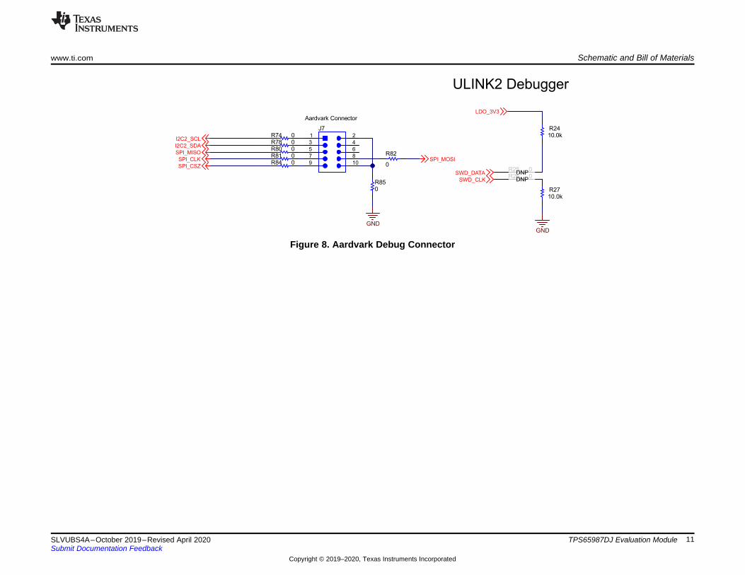
Figure 8. Aardvark Debug Connector
D+1
D-2
GND3
U3
TPD2E009DRTRGND
26 ohmL1
0.01uFC42
WhiteD12
GND
GND
GND
F_USB_D_P F_USB_D_N
10.0kR22
GND
F_VBUS
GND
GND GND
F_SYS_3V3
1
EN2
IN3
IN4
OUT5
OUT6
NC7
PG8
GND
TPS76833QDU13
0.1uF
C21249k
R132
0R133 10µF
C22 10uFC23
VBUS1
D-2
D+3
ID4
GND5
67
8
91
0
J3
F_USB_D_P
F_USB_D_N
Schematic and Bill of Materials www.ti.com
12 SLVUBS4A–October 2019–Revised April 2020Submit Documentation Feedback
Copyright © 2019–2020, Texas Instruments Incorporated
TPS65987DJ Evaluation Module
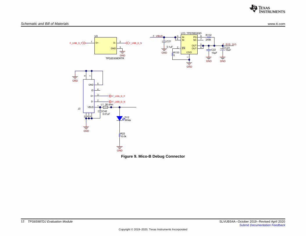
Figure 9. Mico-B Debug Connector

SPI_MISO Pull Downto disable flash config
12
S3
GND
SPI_MISO
0R49
CS1
DO/IO12
WP/IO23
GND4
DI/IO05
CLK6
HOLD/IO37
VCC8
U5
W25Q80DVSNIG
LDO_3V3
0.1uFC29
GND
GNDSPI_CSZ
SPI_CLK
SPI_MOSI
SPI_MISO
3.3kR46
3.3kR47
3.3kR48
3.3kR45 SPI_CSZ
SPI_MISO
0R130
DNP
LDO_3V3
www.ti.com Schematic and Bill of Materials
13SLVUBS4A–October 2019–Revised April 2020Submit Documentation Feedback
Copyright © 2019–2020, Texas Instruments Incorporated
TPS65987DJ Evaluation Module
Figure 10. EEPROM Memory for PD Controller

21
S2
TP2
TP3
SSMX_USB3--> GPIO_2SSMX_FLIP --> GPIO_1SSMX_DP --> GPIO_0
HPD --> GPIO3
SS Mux Control Variable DC/DC Control
Truth TableOutput Voltage
5V
HPD
SSMX_DP
SSMX_FLIP
SSMX_USB3
GPIO_5/I2C3_SCL
GPIO_6/I2C3_SDA
SPI_MISO
SPI_CSZ
SPI_CLK
SPI_MOSI
PDO_1
PDO_0
LDO_3V3
P3V3
LDO_3V3
HRESET
SWD_CLK
I2C1_SCL
I2C1_SDA
I2C2_SCL
I2C2_IRQZ
I2C2_SDA
I2C1_IRQZ
220pFC26
220pFC27
GND
GND
CC1
CC2
C_USB_P
C_USB_N
PP_EXT2_EN
SWD_DATA
PDO_3
/PGOOD
GPIO_7/I2C3_IRQZ
ADCIN2
ADCIN1
GND
PDO_2
PDO_30
PDO_2 PDO_1
00
00
0
0
001
11 9V
15V20V
10.0kR30
10.0kR34
3.83kR28
3.83kR29
3.83kR36
0
R37
100kR38
/FLT_TPD
3.83kR35
0R1350R136
PD_USB_PPD_USB_N
0.01uF
C28
TPS65987DDJRSHR
ADCIN16
ADCIN210
C_CC124
C_CC226
C_USB_N (GPIO19)53
C_USB_P (GPIO18)50
GPIO2155
GPIO2054
GPIO016
GPIO117
GPIO1240
GPIO1341
GPIO14 (PWM)42
GPIO15 (PWM)43
GPIO16 (PP_EXT1)48
GPIO17 (PP_EXT2)49
GPIO218
I2C3_SCL (GPIO5)21
I2C3_SDA (GPIO6)22
I2C3_IRQ (GPIO7)23
GPIO3 (HPD)30
GPIO431
HRESET44
I2C1_IRQ29
I2C1_SCL27
I2C1_SDA28
I2C2_IRQ34
I2C2_SCL32
I2C2_SDA33
SPI_CLK (GPIO10)38
SPI_MISO (GPIO8)36
SPI_MOSI (GPIO9)37
SPI_SS (GPIO11)39
U1A
Schematic and Bill of Materials www.ti.com
14 SLVUBS4A–October 2019–Revised April 2020Submit Documentation Feedback
Copyright © 2019–2020, Texas Instruments Incorporated
TPS65987DJ Evaluation Module
Figure 11. USB PD Controller and Memory

1
2
3
J4
SYS_PWR
VAR_DCDC
PP_HV1
SYS_PWR =>Sinkfrom VBUSVAR_DCDC=>Source to VBUS
1
2
3
J5
SYS_PWR
VAR_DCDC
PP_HV2
SYS_PWR
VAR_DCDC
PP_EXT1
1
2
3
J6
DNP
GND
100uF35V
C52
SYS_PWR
35V220uFC53
Switch 1 On only --> 001b (0.34)Switch 2 On only --> 010b (0.50)Switch 3 On only --> 011b (0.90)
Switch 1-3 Off --> 000b (0)I2C Addr ess Setting
1 2 3 4 5 67891
0
11
12
S4
GNDGND
Switch 4 On only --> BP_WaitFor3V3_Internal (0.24)Switch 4,5 On only --> BP_WaitFor3V3_External (0.44)Switch 6 On only --> BP_NoWait (0.76)
Switch 4-6 Off --> BP_NoResponse (0)BUSPOWERZ Configur ation
ADCIN2 ADCIN1
LDO_3V3
31.6kR44
10.0kR41
100kR40
191kR39
100kR50
100kR51
215kR43
316kR42
www.ti.com Schematic and Bill of Materials
15SLVUBS4A–October 2019–Revised April 2020Submit Documentation Feedback
Copyright © 2019–2020, Texas Instruments Incorporated
TPS65987DJ Evaluation Module
Figure 12. USB PD Controller ADCINx Resistor Divider Settings (for Boot)
Figure 13. Barrel Jack, Variable DC/DC and SYS_PWR
Figure 14. USB PD Power Path Jumpers

GND
10uFC36 GND
10uFC40
GND
10uFC41
DRAIN1
DRAIN2
GND
LDO_3V3
LDO_1V8
P5V010uFC38
4.7uFC37
GND GND
P3V3
PP_HV1
GND
VBUS
PP_CAB_87
22uF
C39
GNDPP_HV2
White
D16
GND
10.0kR66
1uFC5
0R67
0R68
DNP
GND
0R131DNPP3V3
TPS65987DDJRSHR
LDO_1V835
LDO_3V39
DRAIN115
PP_CABLE25
GND46
PP_HV112
PP_HV111
PP_HV21
PP_HV22
VBUS113
VBUS114
VBUS23
VBUS24
VIN_3V35
DRAIN256
DRAIN257
DRAIN27
DRAIN18
DRAIN119
DRAIN158
DRAIN252
GND51
GND20
PAD59
GND45
GND47
U1B
LDO_3V3
LDO_1V8
Schematic and Bill of Materials www.ti.com
16 SLVUBS4A–October 2019–Revised April 2020Submit Documentation Feedback
Copyright © 2019–2020, Texas Instruments Incorporated
TPS65987DJ Evaluation Module
Figure 15. USB PD Power Paths

GND
Q5
22uFC31
3
1
2
4
5
V+
V-
U6
Q6
GND
22uFC30
GND
PP_EXT1 VBUS
GND
GND
PP_EXT2_EN
LDO_3V3
0.1uFC35
100kR62
DNP
10.0kR60
10.0kR57
10.0kR55
1.00k
R61
10.0kR54
DNP10.0kR56
DNP
576k
R65
0.1uFC34DNP
0.1uFC337,8
Q4A
5,6
Q4B
60.4kR59
60.4kR58
10.0kR63
10.0kR64
0.1uFC32
www.ti.com Schematic and Bill of Materials
17SLVUBS4A–October 2019–Revised April 2020Submit Documentation Feedback
Copyright © 2019–2020, Texas Instruments Incorporated
TPS65987DJ Evaluation Module
Figure 16. USB PD External (Sink) Power Path with RCP

22uFC43
22uFC44
GND
GND
Output capacitors must be rated toat least 25V and have ESR in 100s of mOhms
270
R69
0.1uF50V
C45
GND
GND
SYS_PWR
EN_VAR
GND
10kR71
60.4kR21
GND
19.1kR88
0.1uFC49
GreenD20
17.4kR98
Q8 Q10 Q11
Q12
7.15kR99
47uFC46
47uFC47
VAR_DCDC
EN_VAR
PDO_1 PDO_2 PDO_3
GND
PDO_1PDO_20
10
01 00 0
Output Voltage5V9V15V20V
Feedback (R1) Feedback (R2)60.4k60.4k60.4k60.4k
19.1k9.1k5.12k3.9k
Output Voltage5.14V9.3V15.621.03
PDO_3
00
01
Change PDO's
GND
4.70kR100
IN4
IN5
GN
D1
GN
D2
IN6
GN
D3
PA
D7
U9
GND
100kR23
11.0kR72
1000pF
C48
1000pFC511
3
2
D18
DNP
GND
SYS_PWR
1
3
2
D1
10uH
L2
7,81,2,3
5,6,
Q7
47.5kR20
0.1uFC50
SW_Node_VARDC
FB node on VAR_DC
100kR92
100kR95
100kR89
10.0kR73
100kR70
0
R1DNP
GND
TP5
TP4
BlueD19
SENSE1
GND4
POWER2
POWER3
GND5
SHIELD6
SHIELD7
SHIELD8
SHIELD9
J9
JPD1135-509-7F
ISENSE1
GND2
EN3
FB4
ADJ5
PGND6
PGATE7
VIN8
LM3489QMM/NOPB
U8
TP6
GND
Barrel Jack 19.5V @ 4.5A max
GND
PDO_2PDO_1
P3V3
Q14 Q15PDO_0
Q13PDO_3
Q16
10.0kR101
10.0kR102
10.0kR103
10.0kR104
White
D22
White
D23
White
D21
White
D245V 9V 15V 20V
Schematic and Bill of Materials www.ti.com
18 SLVUBS4A–October 2019–Revised April 2020Submit Documentation Feedback
Copyright © 2019–2020, Texas Instruments Incorporated
TPS65987DJ Evaluation Module
Figure 17. Variable DC/DC Control LEDs
Figure 18. Variable DC/DC Controller
SW1
PGND2
IN3
EN4
GND5
ILIM6
ENUSB7
FAULT8
USB9
AUX10
EP11
U12
TPS2500DRCR
0.1uF
C55
0.1uFC57
GND
GND
GND
10uH
L3
GND
0.1uFC68
GND
GND
ILim setMax 1100mATyp 900mAMin 700mA
2.2uH
L4
0.1uFC60
GND
22uFC56
VIN1
VSENSE6
EN8
PGOOD10
GND3
COMP7
PH2
BOOT9
PAD11
GND4
GND5
U10
TPS54334DRCR
2.61kR111
6800pFC64
GND
PG
D_
3V
3
GND
47uFC69
100kR109
32.4kR114
150kR107
66.5kR113
32.4kR116
TP7
TP8
47uFC58
47uFC59
47uF
C65
47uF
C670.1uFC66
47uF
C70
SYS_PWR
P5V0
GND
GND
P3V3
P3V3
P3V3
220pFC62
V3V3_Sense
100k
R115
SW Node Buck
SW Node Boost
PGD_3V3
300pFC63
www.ti.com Schematic and Bill of Materials
19SLVUBS4A–October 2019–Revised April 2020Submit Documentation Feedback
Copyright © 2019–2020, Texas Instruments Incorporated
TPS65987DJ Evaluation Module
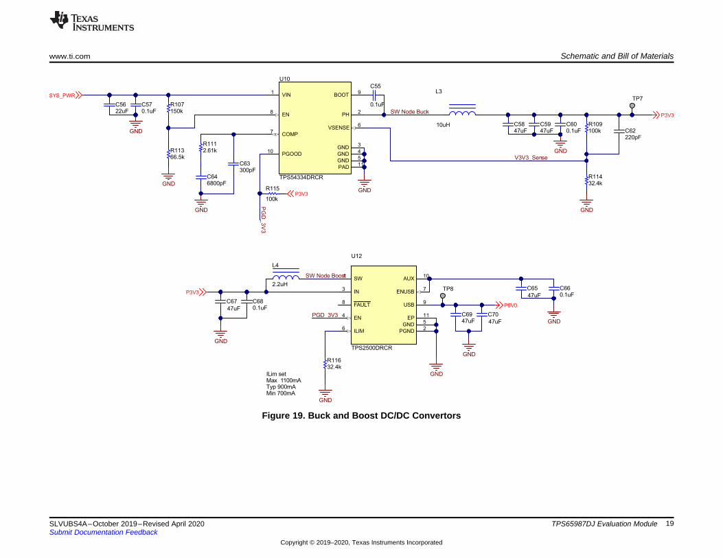
Figure 19. Buck and Boost DC/DC Convertors
Schematic and Bill of Materials www.ti.com
20 SLVUBS4A–October 2019–Revised April 2020Submit Documentation Feedback
Copyright © 2019–2020, Texas Instruments Incorporated
TPS65987DJ Evaluation Module
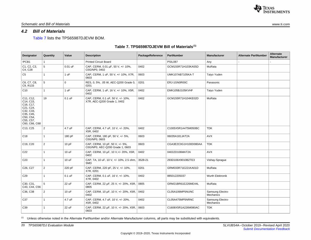
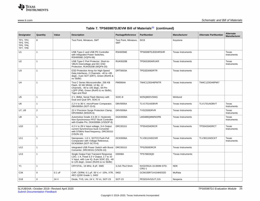
4.2 Bill of MaterialsTable 7 lists the TPS65987DJEVM BOM.
(1) Unless otherwise noted in the Alternate PartNumber and/or Alternate Manufacturer columns, all parts may be substituted with equivalents.
Table 7. TPS65987DJEVM Bill of Materials (1)
Designator Quantity Value Description PackageReference PartNumber Manufacturer Alternate PartNumber AlternateManufacturer
!PCB1 1 Printed Circuit Board PSIL087 Any - -
C1, C2, C3,C4, C28
5 0.01 uF CAP, CERM, 0.01 µF, 50 V, +/- 10%,C0G/NP0, 0402
0402 GCM155R71H103KA55D MuRata
C5 1 1 uF CAP, CERM, 1 uF, 50 V, +/- 10%, X7R,0603
0603 UMK107AB7105KA-T Taiyo Yuden
C6, C7, C8,C9, R133
5 0 RES, 0, 5%, .05 W, AEC-Q200 Grade 0,0201
0201 ERJ-1GN0R00C Panasonic
C10 1 1 uF CAP, CERM, 1 uF, 16 V, +/- 10%, X5R,0402
0402 EMK105BJ105KVHF Taiyo Yuden
C11, C12,C14, C15,C16, C17,C21, C24,C32, C33,C35, C45,C50, C54,C55, C57,C60, C66, C68
19 0.1 uF CAP, CERM, 0.1 uF, 50 V, +/- 10%,X7R, AEC-Q200 Grade 1, 0402
0402 GCM155R71H104KE02D MuRata
C13, C25 2 4.7 uF CAP, CERM, 4.7 uF, 10 V, +/- 20%,X5R, 0402
0402 C1005X5R1A475M050BC TDK
C18 1 180 pF CAP, CERM, 180 pF, 50 V, +/- 5%,C0G/NP0, 0603
0603 06035A181JAT2A AVX
C19, C20 2 10 pF CAP, CERM, 10 pF, 50 V, +/- 5%,C0G/NP0, AEC-Q200 Grade 1, 0603
0603 CGA3E2C0G1H100D080AA TDK
C22 1 10 uF CAP, CERM, 10 µF, 10 V,+/- 20%, X5R,0402
0402 0402ZD106MAT2A AVX
C23 1 10 uF CAP, TA, 10 uF, 10 V, +/- 10%, 2.5 ohm,SMD
3528-21 293D106X9010B2TE3 Vishay-Sprague
C26, C27 2 220 pF CAP, CERM, 220 pF, 25 V, +/- 10%,X7R, 0201
0201 GRM033R71E221KA01D MuRata
C29 1 0.1 uF CAP, CERM, 0.1 uF, 16 V, +/- 10%,X7R, 0402
0402 885012205037 Wurth Elektronik
C30, C31,C43, C44, C56
5 22 uF CAP, CERM, 22 µF, 25 V, +/- 20%, X5R,0805
0805 GRM21BR61E226ME44L MuRata
C36, C38 2 10 uF CAP, CERM, 10 µF, 10 V, +/- 20%, X5R,0402
0402 CL05A106MP5NUNC Samsung Electro-Mechanics
C37 1 4.7 uF CAP, CERM, 4.7 uF, 10 V, +/- 20%,X5R, 0402
0402 CL05A475MP5NRNC Samsung Electro-Mechanics
C39 1 22 uF CAP, CERM, 22 µF, 10 V, +/- 20%, X5R,0603
0603 C1608X5R1A226M080AC TDK

www.ti.com Schematic and Bill of Materials
21SLVUBS4A–October 2019–Revised April 2020Submit Documentation Feedback
Copyright © 2019–2020, Texas Instruments Incorporated
TPS65987DJ Evaluation Module
Table 7. TPS65987DJEVM Bill of Materials (1) (continued)
Designator Quantity Value Description PackageReference PartNumber Manufacturer Alternate PartNumber AlternateManufacturer
C40, C41 2 10 uF CAP, CERM, 10 µF, 25 V, +/- 20%, X5R,0603
0603 GRM188R61E106MA73D MuRata
C42 1 0.01 uF CAP, CERM, 0.01 µF, 50 V,+/- 5%, X7R,0402
0402 C0402C103J5RACTU Kemet
C46, C47 2 47 uF CAP, TA, 47 uF, 35 V, +/- 20%, 0.9 ohm,AEC-Q200 Grade 1, SMD
7343-43 TAJE476M035RNJ AVX
C48, C51 2 1000 pF CAP, CERM, 1000 pF, 50 V,+/- 20%,X7R, 0402
0402 C1005X7R1H102M050BE TDK
C49 1 0.1 uF CAP, CERM, 0.1 uF, 35 V, +/- 10%,X5R, 0402
0402 GMK105BJ104KV-F Taiyo Yuden
C52 1 100 uF CAP, AL, 100 uF, 35 V, +/- 20%, 0.26ohm, AEC-Q200 Grade 2, SMD
D6.3xL5.8mm EEE-FT1V101AP Panasonic
C53 1 220 uF CAP, AL, 220 uF, 35 V, +/- 20%, AEC-Q200 Grade 3, SMD
EEE-1VA221UP Panasonic
C58, C59 2 47 uF CAP, CERM, 47 uF, 6.3 V, +/- 20%,X5R, 0805
0805 GRM219R60J476ME44D MuRata
C61 1 22 pF CAP, CERM, 22 pF, 50 V, +/- 5%,C0G/NP0, AEC-Q200 Grade 1, 0402
0402 GCM1555C1H220JA16D MuRata
C62 1 220 pF CAP, CERM, 220 pF, 50 V, +/- 10%,X7R, AEC-Q200 Grade 1, 0201
0201 CGA1A2X7R1H221K030BA TDK
C63 1 300 pF CAP, CERM, 300 pF, 25 V,+/- 5%,C0G/NP0, 0402
0402 C0402C301J3GAC7867 Kemet
C64 1 6800 pF CAP, CERM, 6800 pF, 50 V,+/- 10%,X7R, 0402
0402 GCM155R71H682KA55D MuRata
C65, C67,C69, C70
4 47 uF CAP, CERM, 47 uF, 6.3 V, +/- 20%,X5R, 0603
0603 GRM188R60J476ME15D MuRata
D1 1 40 V Diode, Schottky, 40 V, 10 A, PowerDI5 PowerDI5 PDS1040L-13 Diodes Inc.
D2, D3, D4,D5, D6, D7,D8, D9, D10,D11
10 1-Channel ESD Protection Diode forUSB Type-C and Thunderbolt 3,DPL0002A (X2SON-2)
DPL0002A TPD1E01B04DPLR Texas Instruments TPD1E01B04DPLT TexasInstruments
D12, D13,D14, D15,D16, D21,D22, D23,D24,
9 White LED, White, SMD 0402, White LW QH8G-Q2S2-3K5L-1 OSRAM LW QH8G-Q2OO-3K5L-1
D17 1 Red LED, Red, SMD 0402 APHHS1005SURCK Kingbright
D19 1 Blue LED, Blue, SMD 1.6x0.8mm LTST-C193TBKT-5A Lite-On
D20 1 Green LED, Green, SMD LED_0603 150060GS75000 Wurth Elektronik
H1, H2, H3,H4
4 Machine Screw, Round, #4-40 x 1/4,Nylon, Philips panhead
Screw NY PMS 440 0025 PH B&F Fastener Supply
H5, H6, H7,H8
4 Standoff, Hex, 0.5"L #4-40 Nylon Standoff 1902C Keystone

Schematic and Bill of Materials www.ti.com
22 SLVUBS4A–October 2019–Revised April 2020Submit Documentation Feedback
Copyright © 2019–2020, Texas Instruments Incorporated
TPS65987DJ Evaluation Module
Table 7. TPS65987DJEVM Bill of Materials (1) (continued)
Designator Quantity Value Description PackageReference PartNumber Manufacturer Alternate PartNumber AlternateManufacturer
J1 1 Receptacle, USB 3.1 Type-C, R/A, Gold,SMT
Receptacle, USB 3.1Type-C, R/A, SMT
DX07S024JJ2R1300 JAE Electronics
J2 1 Socket, 0.8mm, 20x2, Gold, SMT Socket, 0.8mm,20x2, Gold, SMT
LSEM-120-03.0-F-DV-A-N-K-TR
Samtec
J3 1 Connector, Receptacle, Micro-USB TypeAB, R/A, Bottom Mount SMT
Connector,Receptacle, Micro-USB Type AB, R/A,Bottom Mount SMT
ZX62RD-AB-5P8(30) Hirose Electric Co. Ltd.
J4, J5 2 Header, 100mil, 3x1, Gold, TH 3x1 Header TSW-103-07-G-S Samtec
J7 1 Header, 100mil, 5x2, Tin, TH Header, 5x2, 100mil,Tin
PEC05DAAN Sullins ConnectorSolutions
J8 1 Header, 100mil, 4x1, Tin, TH Header, 4x1, 100mil,TH
PEC04SAAN Sullins ConnectorSolutions
J9 1 Connector, DC Power Jack, R/A, 3 Pos,TH
Power connector JPD1135-509-7F Foxconn
L1 1 26 ohm Ferrite Bead, 26 ohm at 100 MHz, 6 A,0603
0603 BLM18SG260TN1D MuRata
L2 1 10 uH Inductor, Shielded, Powdered Iron, 10µH, 7.5 A, 0.03 ohm, AEC-Q200 Grade1, SMD
11x10mm SRP1038A-100M Bourns
L3 1 10 uH Inductor, Shielded, 10 µH, 4 A, 0.068ohm, SMD
7.2 mm x 6.65 mm ASPI-0630LR-100M-T15 Abracon Corporation - -
L4 1 2.2 uH Inductor, Shielded, Powdered Iron, 2.2uH, 4.7 A, 0.035 ohm, AEC-Q200 Grade1, SMD
4.1 mm x 4.1 mm 78438356022 Wurth Elektronik
Q1, Q2, Q3 3 20 V MOSFET, N-CH, 20 V, 0.6 A, SOT-416 SOT-416 SI1012R-T1-GE3 Vishay-Siliconix None
Q4 1 –30 V MOSFET, 2-CH, P-CH, -30 V, -60 A,610x604x515mm
610x604x515mm SI7997DP-T1-GE3 Vishay-Siliconix None
Q5 1 30 V MOSFET, N-CH, 30 V, 0.35 A, AEC-Q101, SOT-323
SOT-323 NX3008NBKW,115 Nexperia None
Q6 1 20 V MOSFET, N-CH, 20 V, 0.5 A,YJM0003A (PICOSTAR-3)
YJM0003A CSD15380F3 Texas Instruments None
Q7 1 –30 V MOSFET, P-CH, -30 V, -11 A, FET,3x0.8x3mm
FET, 3x0.8x3mm AONR21321 AOS AON7403 None
Q8, Q10, Q11 3 20 V MOSFET, N-CH, 20 V, 1.05 A, SOT-23 SOT-23 BSH105,215 Nexperia None
Q9 1 –20 V MOSFET, P-CH, -20 V, -0.76 A, SOT-416
SOT-416 NTA4151PT1G ON Semiconductor None
Q12, Q13,Q14, Q15,Q16
5 30 V MOSFET, N-CH, 30 V, 0.18 A, SOT-323 SOT-323 NX3020NAKW,115 Nexperia None
R6, R8, R10 3 0 RES, 0, 5%, 0.1 W, AEC-Q200 Grade 0,0402
0402 ERJ-2GE0R00X Panasonic
R12, R13, R14 3 10.0 k RES, 10.0 k, 1%, 0.063 W, AEC-Q200Grade 0, 0402
0402 CRCW040210K0FKED Vishay-Dale

www.ti.com Schematic and Bill of Materials
23SLVUBS4A–October 2019–Revised April 2020Submit Documentation Feedback
Copyright © 2019–2020, Texas Instruments Incorporated
TPS65987DJ Evaluation Module
Table 7. TPS65987DJEVM Bill of Materials (1) (continued)
Designator Quantity Value Description PackageReference PartNumber Manufacturer Alternate PartNumber AlternateManufacturer
R15, R16,R17, R18,R19, R52,R53, R75,R86, R87,R90, R91,R94, R97,R134, R135,R136
17 0 RES, 0, 5%, 0.05 W, 0201 0201 CRCW02010000Z0ED Vishay-Dale
R20 1 47.5 k RES, 47.5 k, 1%, 0.063 W, AEC-Q200Grade 0, 0402
0402 CRCW040247K5FKED Vishay-Dale
R21, R58, R59 3 60.4 k RES, 60.4 k, 1%, 0.063 W, AEC-Q200Grade 0, 0402
0402 CRCW040260K4FKED Vishay-Dale
R22, R30,R32, R33,R34, R41,R55, R57,R60, R63,R64, R66,R73, R101,R102, R103,R104
17 10.0 k RES, 10.0 k, 1%, 0.1 W, 0402 0402 ERJ-2RKF1002X Panasonic
R23, R38,R40, R50,R51, R70,R89, R92,R95, R105,R109, R115
12 100 k RES, 100 k, 1%, 0.063 W, AEC-Q200Grade 0, 0402
0402 CRCW0402100KFKED Vishay-Dale
R24, R27 2 10.0 k RES, 10.0 k, 1%, 0.1 W, 0603 0603 RC0603FR-0710KL Yageo
R28, R29,R35, R36
4 3.83 k RES, 3.83 k, 1%, 0.063 W, AEC-Q200Grade 0, 0402
0402 CRCW04023K83FKED Vishay-Dale
R31 1 10.0 k RES, 10.0 k, 0.5%, 0.063 W, AEC-Q200Grade 0, 0402
0402 CRCW040210K0DHEDP Vishay-Dale
R37, R49,R67, R74,R76, R77,R78, R80,R81, R82,R84, R85
12 0 RES, 0, 5%, 0.063 W, 0402 0402 RC0402JR-070RL Yageo America
R39 1 191 k RES, 191 k, 1%, 0.063 W, AEC-Q200Grade 0, 0402
0402 CRCW0402191KFKED Vishay-Dale
R42 1 316 k RES, 316 k, 1%, 0.063 W, AEC-Q200Grade 0, 0402
0402 CRCW0402316KFKED Vishay-Dale
R43 1 215 k RES, 215 k, 1%, 0.063 W, 0402 0402 CRCW0402215KFKED Vishay-Dale
R44 1 31.6 k RES, 31.6 k, 1%, 0.063 W, AEC-Q200Grade 0, 0402
0402 CRCW040231K6FKED Vishay-Dale
R45, R46,R47, R48
4 3.3 k RES, 3.3 k, 5%, 0.063 W, AEC-Q200Grade 0, 0402
0402 CRCW04023K30JNED Vishay-Dale

Schematic and Bill of Materials www.ti.com
24 SLVUBS4A–October 2019–Revised April 2020Submit Documentation Feedback
Copyright © 2019–2020, Texas Instruments Incorporated
TPS65987DJ Evaluation Module
Table 7. TPS65987DJEVM Bill of Materials (1) (continued)
Designator Quantity Value Description PackageReference PartNumber Manufacturer Alternate PartNumber AlternateManufacturer
R61 1 1.00 k RES, 1.00 k, 1%, 0.1 W, 0402 0402 ERJ-2RKF1001X Panasonic
R65 1 576 k RES, 576 k, 1%, 0.063 W, AEC-Q200Grade 0, 0402
0402 CRCW0402576KFKED Vishay-Dale
R69 1 270 RES, 270, 5%, 0.063 W, AEC-Q200Grade 0, 0402
0402 CRCW0402270RJNED Vishay-Dale
R71 1 10 k RES, 10 k, 5%, 0.1 W, 0603 0603 RC0603JR-0710KL Yageo
R72 1 11.0 k RES, 11.0 k, 1%, 0.063 W, AEC-Q200Grade 0, 0402
0402 CRCW040211K0FKED Vishay-Dale
R79 1 100 k RES, 100 k, 5%, 0.05 W, 0201 0201 RC0201JR-7D100KL Yageo America
R83 1 10.0 k RES, 10.0 k, 1%, 0.063 W, 0402 0402 RC0402FR-0710KL Yageo America
R88 1 19.1 k RES, 19.1 k, 1%, 0.063 W, AEC-Q200Grade 0, 0402
0402 CRCW040219K1FKED Vishay-Dale
R98 1 17.4 k RES, 17.4 k, 1%, 0.063 W, AEC-Q200Grade 0, 0402
0402 CRCW040217K4FKED Vishay-Dale
R99 1 7.15 k RES, 7.15 k, 1%, 0.063 W, AEC-Q200Grade 0, 0402
0402 CRCW04027K15FKED Vishay-Dale
R100 1 4.70 k RES, 4.70 k, 1%, 0.0625 W, 0402 0402 RC0402FR-074K7L Yageo America
R106 1 0 RES, 0, 5%, 0.063 W, AEC-Q200 Grade0, 0402
0402 CRCW04020000Z0ED Vishay-Dale
R107 1 150 k RES, 150 k, 1%, 0.063 W, AEC-Q200Grade 0, 0402
0402 CRCW0402150KFKED Vishay-Dale
R108 1 15.0 k RES, 15.0 k, 1%, 0.063 W, AEC-Q200Grade 0, 0402
0402 CRCW040215K0FKED Vishay-Dale
R110 1 39 k RES, 39 k, 5%, 0.063 W, AEC-Q200Grade 0, 0402
0402 CRCW040239K0JNED Vishay-Dale
R111 1 2.61 k RES, 2.61 k, 1%, 0.063 W, AEC-Q200Grade 0, 0402
0402 CRCW04022K61FKED Vishay-Dale
R112 1 560 k RES, 560 k, 5%, 0.063 W, AEC-Q200Grade 0, 0402
0402 CRCW0402560KJNED Vishay-Dale
R113 1 66.5 k RES, 66.5 k, 1%, 0.063 W, AEC-Q200Grade 0, 0402
0402 CRCW040266K5FKED Vishay-Dale
R114, R116 2 32.4 k RES, 32.4 k, 1%, 0.063 W, AEC-Q200Grade 0, 0402
0402 CRCW040232K4FKED Vishay-Dale
R132 1 249 k RES, 249 k, 1%, 0.1 W, AEC-Q200Grade 0, 0603
0603 CRCW0603249KFKEA Vishay-Dale
S1, S2 2 SWITCH TACTILE SPST-NO 0.05A 12V
3x1.6x2.5mm B3U-1000P Omron ElectronicComponents
S3 1 Switch, Slide, SPST, Top Slide, SMT Switch, Single TopSlide, 2.5x8x2.5mm
CHS-01TB Copal Electronics
S4 1 DIP Switch, SPST, 6Pos, Slide, SMT 8.75x6.2mm TDA06H0SB1 C&K Components
SH-J1, SH-J2 2 1x2 Shunt, 100mil, Gold plated, Black Shunt SNT-100-BK-G Samtec 969102-0000-DA 3M
www.ti.com Schematic and Bill of Materials
25SLVUBS4A–October 2019–Revised April 2020Submit Documentation Feedback
Copyright © 2019–2020, Texas Instruments Incorporated
TPS65987DJ Evaluation Module
Table 7. TPS65987DJEVM Bill of Materials (1) (continued)
Designator Quantity Value Description PackageReference PartNumber Manufacturer Alternate PartNumber AlternateManufacturer
TP1, TP2,TP3, TP4,TP5, TP6,TP7, TP8
8 Test Point, Miniature, SMT Test Point, Miniature,SMT
5019 Keystone
U1 1 USB Type-C and USB PD Controllerwith Integrated Power Switches,RSH0056E (VQFN-56)
RSH0056E TPS65987DJDDHRSHR Texas Instruments TexasInstruments
U2 1 USB Type-C Port Protector: Short-to-VBUS Overvoltage and IEC ESDProtection, RUK0020B (WQFN-20)
RUK0020B TPD6S300ARUKR Texas Instruments TexasInstruments
U3 1 ESD Protection Array for High-SpeedData Interfaces, 2 Channels, -40 to +85degC, 3-pin SOT (DRT), Green (RoHS &no Sb/Br)
DRT0003A TPD2E009DRTR Texas Instruments
U4 1 Tiva C Series Microcontroller, 256 KBFlash, 32 KB SRAM, 12 Bit, 12Channels, -40 to 105 degC, 64-PinLQFP (PM), Green (RoHS & no Sb/Br),Tape and Reel
PM0064A TM4C123GH6PMTR Texas Instruments TM4C123GH6PMI7
U5 1 3 V, 8Mbit, Serial Flash Memory withDual and Qual SPI, SOIC-8
SOIC-8 W25Q80DVSNIG Winbond
U6 1 2.2-V to 36-V, microPower Comparator,DBV0005A (SOT-23-5)
DBV0005A TLV1701AIDBVR Texas Instruments TLV1701AIDBVT TexasInstruments
U7, U9 2 22-V Precision Surge Protection Clamp,DRV0006A (WSON-6)
DRV0006A TVS2200DRVR Texas Instruments TexasInstruments
U8 1 Automotive Grade 4.5-35 V, HystereticNon-Synchronous PFET Buck Controllerwith Enable Pin, DGK0008A (VSSOP-8)
DGK0008A LM3489QMM/NOPB Texas Instruments TexasInstruments
U10 1 4.2-V to 28-V Input voltage, 3-A Outputcurrent Synchronous buck Converterwith 570kHz fixed frequency, DRC0010J(VSON-10)
DRC0010J TPS54334DRCR Texas Instruments TPS54334DRCT TexasInstruments
U11 1 Nanopower, 1.8 V, SOT23 Push-PullComparator with Voltage Reference,DCK0006A (SOT-SC70-6)
DCK0006A TLV3012AIDCKR Texas Instruments TLV3012AIDCKT TexasInstruments
U12 1 Integrated USB Power Switch with BoostConverter, DRC0010J (VSON-10)
DRC0010J TPS2500DRCR Texas Instruments
U13 1 Single Output Fast Transient ResponseLDO, 1 A, Fixed 3.3 V Output, 2.7 to 10V Input, with Low IQ, 8-pin SOIC (D), -40to 125 degC, Green (RoHS & no Sb/Br)
D0008A TPS76833QD 'Texas Instruments
Y1 1 CRYSTAL, 16 MHz, 8 pF, SMD 3.2x0.75x2.5mm NX3225GA-16.000M-STD-CRG-1
NDK
C34 0 0.1 uF CAP, CERM, 0.1 µF, 50 V,+/- 10%, X7R,AEC-Q200 Grade 1, 0402
0402 GCM155R71H104KE02D MuRata
D18 0 24 V Diode, TVS, Uni, 24 V, 70 Vc, SOT-23 SOT-23 PESD24VS2UT,215 Nexperia

Schematic and Bill of Materials www.ti.com
26 SLVUBS4A–October 2019–Revised April 2020Submit Documentation Feedback
Copyright © 2019–2020, Texas Instruments Incorporated
TPS65987DJ Evaluation Module
Table 7. TPS65987DJEVM Bill of Materials (1) (continued)
Designator Quantity Value Description PackageReference PartNumber Manufacturer Alternate PartNumber AlternateManufacturer
FID1, FID2,FID3, FID4,FID5, FID6
0 Fiducial mark. There is nothing to buy ormount.
N/A N/A N/A
J6 0 Header, 100mil, 3x1, Gold, TH 3x1 Header TSW-103-07-G-S Samtec
R1, R7, R9,R11
0 0 RES, 0, 5%, 0.1 W, AEC-Q200 Grade 0,0402
0402 ERJ-2GE0R00X Panasonic
R2, R3, R4,R5
0 0 RES, 0, 5%, 0.05 W, 0201 0201 CRCW02010000Z0ED Vishay-Dale
R25, R26,R68, R93,R96, R130,R131
0 0 RES, 0, 5%, 0.063 W, 0402 0402 RC0402JR-070RL Yageo America
R54, R56 0 10.0 k RES, 10.0 k, 1%, 0.1 W, 0402 0402 ERJ-2RKF1002X Panasonic
R62 0 100 k RES, 100 k, 1%, 0.063 W, AEC-Q200Grade 0, 0402
0402 CRCW0402100KFKED Vishay-Dale
www.ti.com Revision History
27SLVUBS4A–October 2019–Revised April 2020Submit Documentation Feedback
Copyright © 2019–2020, Texas Instruments Incorporated
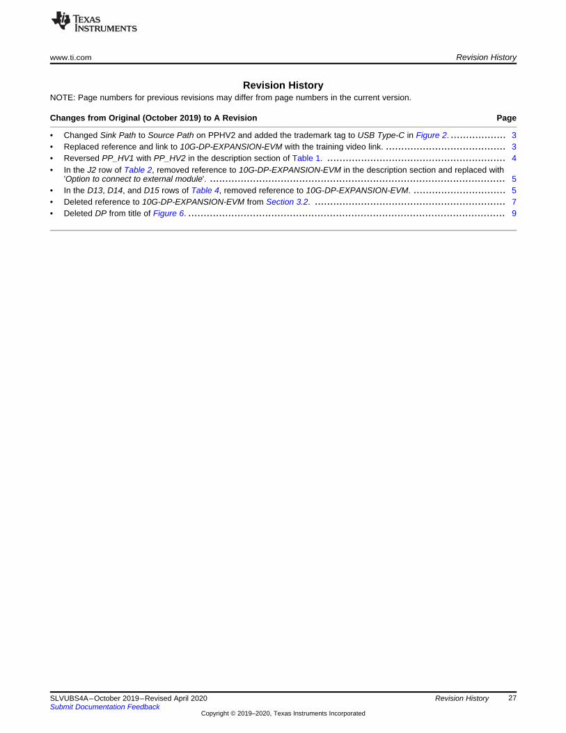
Revision History
Revision HistoryNOTE: Page numbers for previous revisions may differ from page numbers in the current version.
Changes from Original (October 2019) to A Revision .................................................................................................... Page
• Changed Sink Path to Source Path on PPHV2 and added the trademark tag to USB Type-C in Figure 2. .................. 3• Replaced reference and link to 10G-DP-EXPANSION-EVM with the training video link. ....................................... 3• Reversed PP_HV1 with PP_HV2 in the description section of Table 1. .......................................................... 4• In the J2 row of Table 2, removed reference to 10G-DP-EXPANSION-EVM in the description section and replaced with
'Option to connect to external module'. ................................................................................................ 5• In the D13, D14, and D15 rows of Table 4, removed reference to 10G-DP-EXPANSION-EVM. .............................. 5• Deleted reference to 10G-DP-EXPANSION-EVM from Section 3.2. .............................................................. 7• Deleted DP from title of Figure 6. ....................................................................................................... 9
IMPORTANT NOTICE AND DISCLAIMER
TI PROVIDES TECHNICAL AND RELIABILITY DATA (INCLUDING DATASHEETS), DESIGN RESOURCES (INCLUDING REFERENCE DESIGNS), APPLICATION OR OTHER DESIGN ADVICE, WEB TOOLS, SAFETY INFORMATION, AND OTHER RESOURCES “AS IS” AND WITH ALL FAULTS, AND DISCLAIMS ALL WARRANTIES, EXPRESS AND IMPLIED, INCLUDING WITHOUT LIMITATION ANY IMPLIED WARRANTIES OF MERCHANTABILITY, FITNESS FOR A PARTICULAR PURPOSE OR NON-INFRINGEMENT OF THIRD PARTY INTELLECTUAL PROPERTY RIGHTS.These resources are intended for skilled developers designing with TI products. You are solely responsible for (1) selecting the appropriate TI products for your application, (2) designing, validating and testing your application, and (3) ensuring your application meets applicable standards, and any other safety, security, or other requirements. These resources are subject to change without notice. TI grants you permission to use these resources only for development of an application that uses the TI products described in the resource. Other reproduction and display of these resources is prohibited. No license is granted to any other TI intellectual property right or to any third party intellectual property right. TI disclaims responsibility for, and you will fully indemnify TI and its representatives against, any claims, damages, costs, losses, and liabilities arising out of your use of these resources.TI’s products are provided subject to TI’s Terms of Sale (www.ti.com/legal/termsofsale.html) or other applicable terms available either on ti.com or provided in conjunction with such TI products. TI’s provision of these resources does not expand or otherwise alter TI’s applicable warranties or warranty disclaimers for TI products.
Mailing Address: Texas Instruments, Post Office Box 655303, Dallas, Texas 75265Copyright © 2020, Texas Instruments Incorporated