Embed Size (px)
Citation preview

TPS563211 4.2-V to 18-V Input, 3-A Synchronous Buck Converter in SOT583 Package
1 Features• Input voltage: 4.2 V to 18 V• Output voltage: 0.6 V to 7 V
– Up to 3-A continuous output current– Minimum switching on time: 45 ns– Maximum duty cycle: 98%
• High efficiency– Integrated 66-mΩ and 33-mΩ MOSFETs– Quiescent current 120-μA typical
• Highly flexible and easy to use– Selectable Eco-mode or FCCM operation– Selectable power good indicator or external soft
start– Precise enable input
• High accuracy– Reference voltage accuracy: ±1% (25°C)– Switching frequency tolerance: ±8.5%
• Small solution size– Internal compensation for ease of use– SOT583 package– Minimum external components
• Cycle-by-cycle current limit for both high-side and low-side MOSFETs
• Non-latched OVP, UVP, UVLO, and TSD protections
• Create a custom design using TPS563211 with the WEBENCH® Power Designer
2 Applications• Set-top box (STB), digital TV• Smart speaker• Wired networking, broadband• Surveillance
3 DescriptionThe TPS563211 is a cost effective and highly flexible synchronous buck converter that provides selectable Eco-mode operation or FCCM (Force Continuous Conduction Mode) operation. A selectable Power-Good indicator or external soft start is also configurable through the MODE pin. Power sequencing is possible by correctly configuring Enable, Power-Good indicator, or external soft start. A wide input voltage range of 4.2 V to 18 V supports a wide variety of common input rails like 12 V and 15 V. It supports up to 3-A continuous output current at output voltages between 0.6 V and 7 V.
The device provides fast transient response with true fixed switching frequency through the use of the Advanced Emulated Current Mode (AECM) control topology. With internal smart loop bandwidth control, the device provides fast transient response over a wide output voltage range without the need for external compensation.
Cycle-by-cycle current limit on the high-side peak current protects the device in overload situations and is enhanced by a low-side valley current limit, which prevents current runaway. Hiccup mode would be triggered under overvoltage protection (OVP), undervoltage protection (UVP), UVLO protection, and thermal shutdown.
The device is available in 1.6-mm × 2.1-mm SOT583 package.
Device InformationPART NUMBER PACKAGE(1) BODY SIZE (NOM)
TPS563211 SOT583 (8) 1.2 mm × 2.1 mm
(1) For all available packages, see the orderable addendum at the end of the data sheet.
VIN
EN
MODE
BOOT
PG/SS
SW
C1 L
R1
R2
C3
C2
GND FB
VIN
VOUT
EN
TPS563211
R3
Simplified SchematicOutput Current (A)
Effic
iency (
%)
0.001 0.01 0.1 1 5550
55
60
65
70
75
80
85
90
95
100
VIN = 12 V, VOUT = 3.3 VVIN = 12 V, VOUT = 5 VVIN = 9 V, VOUT = 3.3 VVIN = 9 V, VOUT = 5 V
Efficiency vs Output Current
TPS563211SLUSDX1A – SEPTEMBER 2020 – REVISED AUGUST 2021
An IMPORTANT NOTICE at the end of this data sheet addresses availability, warranty, changes, use in safety-critical applications, intellectual property matters and other important disclaimers. PRODUCTION DATA.

Table of Contents1 Features............................................................................12 Applications..................................................................... 13 Description.......................................................................14 Revision History.............................................................. 25 Pin Configuration and Functions...................................36 Specifications.................................................................. 4
6.1 Absolute Maximum Ratings ....................................... 46.2 ESD Ratings .............................................................. 46.3 Recommended Operating Conditions ........................46.4 Thermal Information ...................................................56.5 Electrical Characteristics ............................................56.6 Typical Characteristics................................................ 7
7 Detailed Description......................................................107.1 Overview................................................................... 107.2 Functional Block Diagram......................................... 107.3 Feature Description...................................................107.4 Device Functional Modes..........................................15
8 Application and Implementation.................................. 178.1 Application Information............................................. 178.2 Typical Application.................................................... 17
9 Power Supply Recommendations................................2610 Layout...........................................................................26
10.1 Layout Guidelines................................................... 2610.2 Layout Example...................................................... 26
11 Device and Documentation Support..........................2811.1 Device Support........................................................2811.2 Receiving Notification of Documentation Updates.. 2811.3 Support Resources................................................. 2811.4 Trademarks............................................................. 2811.5 Electrostatic Discharge Caution.............................. 2811.6 Glossary.................................................................. 28
12 Mechanical, Packaging, and Orderable Information.................................................................... 29
4 Revision HistoryNOTE: Page numbers for previous revisions may differ from page numbers in the current version.
Changes from Revision * (September 2020) to Revision A (August 2021) Page• Changed document status from Advance Information to Production Data.........................................................1
TPS563211SLUSDX1A – SEPTEMBER 2020 – REVISED AUGUST 2021 www.ti.com
2 Submit Document Feedback Copyright © 2021 Texas Instruments Incorporated
Product Folder Links: TPS563211
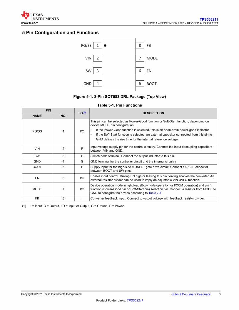
5 Pin Configuration and Functions
PG/SS 1
2
3
4
8
7
6
5
VIN
SW
GND BOOT
EN
MODE
FB
Figure 5-1. 8-Pin SOT583 DRL Package (Top View)
Table 5-1. Pin FunctionsPIN
I/O(1) DESCRIPTIONNAME NO.
PG/SS 1 I/O
This pin can be selected as Power-Good function or Soft-Start function, depending on device MODE pin configuration.• If the Power-Good function is selected, this is an open-drain power-good indicator.• If the Soft-Start function is selected, an external capacitor connected from this pin to
GND defines the rise time for the internal reference voltage.
VIN 2 P Input voltage supply pin for the control circuitry. Connect the input decoupling capacitors between VIN and GND.
SW 3 P Switch node terminal. Connect the output inductor to this pin.
GND 4 G GND terminal for the controller circuit and the internal circuitry
BOOT 5 P Supply input for the high-side MOSFET gate drive circuit. Connect a 0.1-µF capacitor between BOOT and SW pins.
EN 6 I/O Enable input control. Driving EN high or leaving this pin floating enables the converter. An external resistor divider can be used to imply an adjustable VIN UVLO function.
MODE 7 I/ODevice operation mode in light load (Eco-mode operation or FCCM operation) and pin 1 function (Power-Good pin or Soft-Start pin) selection pin. Connect a resistor from MODE to GND to configure the device according to Table 7-1.
FB 8 I Converter feedback input. Connect to output voltage with feedback resistor divider.
(1) I = Input, O = Output, I/O = Input or Output, G = Ground, P = Power
www.ti.comTPS563211
SLUSDX1A – SEPTEMBER 2020 – REVISED AUGUST 2021
Copyright © 2021 Texas Instruments Incorporated Submit Document Feedback 3
Product Folder Links: TPS563211

6 Specifications6.1 Absolute Maximum RatingsOver the recommended operating junction temperature range of –40°C to +125°C (unless otherwise noted)(1)
MIN MAX UNIT
Pin voltage(2)
VIN –0.3 20
V
SW, DC –0.3 20
SW, transient < 10 ns –3 22
VIN – SW, DC –0.3 20
VIN – SW, transient < 10 ns –3 22
BOOT –0.3 25
BOOT – SW –0.3 6
EN, FB, PG/SS, MODE –0.3 6
TJ Operating junction temperature(3) –40 150 °C
Tstg Storage temperature –65 150 °C
(1) Stresses beyond those listed under Absolute Maximum Ratings may cause permanent damage to the device. These are stress ratings only, which do not imply functional operation of the device at these or any other conditions beyond those indicated under Recommended Operating Conditions. Exposure to absolute-maximum-rated conditions for extended periods may affect device reliability.
(2) All voltage values are with respect to the network ground terminal.(3) Operating at junction temperatures greater than 125°C, although possible, degrades the lifetime of the device.
6.2 ESD RatingsVALUE UNIT
V(ESD) Electrostatic discharge
Human body model (HBM), per ANSI/ESDA/JEDEC JS-001, all pins(1) ±2000
VCharged device model (CDM), per JEDEC specification JESD22-C101, all pins(2)
±500
(1) JEDEC document JEP155 states that 500-V HBM allows safe manufacturing with a standard ESD control process.(2) JEDEC document JEP157 states that 250-V CDM allows safe manufacturing with a standard ESD control process.
6.3 Recommended Operating ConditionsOver the recommended operating junction temperature range of –40°C to +125°C (unless otherwise noted)(1)
MIN MAX UNITVIN Input supply voltage range 4.2 18
V
VOUT Output voltage range 0.6 7
Pin voltage
SW, DC –0.1 18
SW, transient < 10 ns –3 20
VIN - SW, DC –0.1 18
VIN - SW, transient < 10 ns –3 20
BOOT –0.1 23.5
BOOT - SW –0.1 5.5
EN, FB, PG/SS, MODE –0.1 5.5
IOUT Output current range 0 3 A
TJ Operating junction temperature –40 125 °C
(1) Recommended Operating Conditions indicate conditions for which the device is intended to be functional, but do not guarantee specific performance limits. For ensured specifications, see the Electrical Characteristics.
TPS563211SLUSDX1A – SEPTEMBER 2020 – REVISED AUGUST 2021 www.ti.com
4 Submit Document Feedback Copyright © 2021 Texas Instruments Incorporated
Product Folder Links: TPS563211

6.4 Thermal Information
THERMAL METRIC(1)
TPS563211UNITDRL (SOT583)
8 PINSRθJA (2) Junction-to-ambient thermal resistance 116.7 °C/W
RθJC(top) Junction-to-case (top) thermal resistance 41.7 °C/W
RθJB Junction-to-board thermal resistance 20.9 °C/W
ΨJTJunction-to-top characterization parameter 1.0 °C/W
ΨJBJunction-to-board characterization parameter 20.8 °C/W
RθJA(EVM) (3) Junction-to-ambient thermal resistance on TPS563211EVM 70 °C/W
(1) For more information about traditional and new thermal metrics, see the Semiconductor and IC Package Thermal Metrics application report, SPRA953
(2) The value of RθJA given in this table is only valid for comparison with other packages and can not be used for design purposes. These values were simulated on a standard JEDEC board. They do not represent the performance obtained in an actual application.
(3) The real RθJA on the TPS563211EVM is about 70 ℃/W, test condition: VIN = 12 V, VOUT = 5 V, IOUT = 3 A, TA = 25 ℃.
6.5 Electrical CharacteristicsLimits apply over the recommended operating junction temperature (TJ ) range of –40°C to +125°C, unless otherwise stated. Minimum and maximum limits are specified through test, design or statistical correlation. Typical values represent the most likely parametric norm at TJ = 25°C, and are provided for reference purposes only. Unless otherwise stated, the following conditions apply: VIN = 4.2 V to 18 V.
PARAMETER TEST CONDITIONS MIN TYP MAX UNITSUPPLYVIN Operation input voltage 4.2 18 V
IQ(VIN)
VIN quiescent current at power save mode
Nonswitching, VEN = 1.2 V, VFB = 0.65 V, IOUT = 0 mA 120 µA
VIN quiescent current at FCCM Nonswitching, VEN = 1.2 V, VFB = 0.65 V, IOUT = 0 mA 450 µA
ISD(VIN) VIN shutdown supply current VIN = 12 V, VEN = 0 V 3 10 µA
UVLOVUVLO(R) VIN UVLO rising threshold VIN rising 3.8 4 4.2 V
VUVLO(F) VIN UVLO falling threshold VIN falling 3.4 3.6 3.8 V
ENABLEVEN(R) EN voltage rising threshold EN rising, enable switching 1.05 1.15 1.25 V
VEN(F) EN voltage falling threshold EN falling, disable switching 0.91 1.01 1.10 V
IEN(P1)EN pin sourcing current pre EN rising threshold VEN = 1.0 V 0.93 1.2 1.5 µA
IEN(H) EN pin sourcing current hysteresis 2.4 3.1 3.81 µA
REFERENCE VOLTAGE
VFB FB voltageTJ = 25°C 0.594 0.6 0.606 V
TJ = –40°C to 125°C, VIN = 12 V 0.591 0.6 0.609 V
IFB(LKG) FB input leakage current VFB = 0.65 V, TJ = 25°C –0.1 0 0.1 µA
STARTUPISS Soft-start charge current VSS = 0 V 4.5 6.6 8.3 µA
tSS Internal fixed soft-start time From 1st switching pulse until target VOUT
1.5 2 2.6 ms
SWITCHING FREQUENCYfSW(FCCM) Switching frequency, FCCM operation 550 600 650 kHz
POWER STAGE
www.ti.comTPS563211
SLUSDX1A – SEPTEMBER 2020 – REVISED AUGUST 2021
Copyright © 2021 Texas Instruments Incorporated Submit Document Feedback 5
Product Folder Links: TPS563211

Limits apply over the recommended operating junction temperature (TJ ) range of –40°C to +125°C, unless otherwise stated. Minimum and maximum limits are specified through test, design or statistical correlation. Typical values represent the most likely parametric norm at TJ = 25°C, and are provided for reference purposes only. Unless otherwise stated, the following conditions apply: VIN = 4.2 V to 18 V.
PARAMETER TEST CONDITIONS MIN TYP MAX UNITRDSON(HS) High-side MOSFET on-resistance TJ = 25°C, VIN = 12 V, VBOOT-SW = 5 V 66 mΩ
RDSON(LS) Low-side MOSFET on-resistance TJ = 25°C, VIN = 12 V 33 mΩ
tON(min) (1) Minimum ON pulse width 45 ns
tON(max) Maximum ON pulse width 6 µs
tOFF(min) Minimum OFF pulse width 105 ns
OVERCURRENT PROTECTIONIHS(OC) High-side peak current limit Peak current limit on the HS MOSFET 4.25 5 5.75 A
ILS(OC) Low-side valley current limit Valley current limit on the LS MOSFET, VIN = 12 V 3.0 4 4.9 A
ILS(NOC) Low-side negative current limit for FCCM Sinking current limit on the LS MOSFET, VIN = 12 V 1.1 1.5 2.2 A
tHIC(WAIT) Wait time before entering Hiccup 108 µs
tHIC(RE) Hiccup time before re-start 6 Cycles
OUTPUT OVP AND UVP
VUVPUndervoltage-protection (UVP) threshold voltage
VFB falling 62.5%
UVP hysteresis 5%
VOVPOvervoltage-protection (OVP) threshold voltage
VFB rising 107% 112.0% 114%
OVP hysteresis 5%
POWER GOOD
VPGTH Power-good threshold
FB falling, PG from high to low 82% 87% 92%
FB rising, PG from low to high 87% 92% 97%
FB falling, PG from low to high 101% 107% 112%
FB rising, PG from high to low 107% 112% 114%
VPG(OL) PG pin output low-level voltage IPG = 0.6 mA 0.3 V
IPG(LKG)PG pin leakage current when open drain output is high VPG = 5.5 V –1 1 µA
tPG(R) PG delay going from low to high 112 µs
tPG(F) PG delay going from high to low 48 µs
Minimum VIN for valid output(1) VPG/SS < 0.5 V at 100 μA 2 2.5 V
THERMAL SHUTDOWNTJ(SD) (1) Thermal shutdown threshold 150 °C
TJ(HYS) (1) Thermal shutdown hysteresis 20 °C
(1) Not production tested
TPS563211SLUSDX1A – SEPTEMBER 2020 – REVISED AUGUST 2021 www.ti.com
6 Submit Document Feedback Copyright © 2021 Texas Instruments Incorporated
Product Folder Links: TPS563211

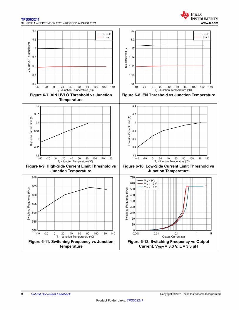
6.6 Typical CharacteristicsVIN = 12 V, TA = 25°C, unless otherwise noted.
TJ - Junction Temperature (qC)
Qu
iesce
nt
Cu
rre
nt
(PA
)
-40 -20 0 20 40 60 80 100 120 140114
116
118
120
122
124
126
128
130
132
Figure 6-1. Quiescent Current (Eco Mode) vs Junction Temperature
TJ - Junction Temperature (qC)
Qu
iesce
nt
Cu
rre
nt
(PA
)
-40 -20 0 20 40 60 80 100 120 140410
420
430
440
450
460
470
480
490
500
Figure 6-2. Quiescent Current (FCCM) vs Junction Temperature
TJ - Junction Temperature (qC)
Sh
utd
ow
n C
urr
en
t (P
A)
-40 -20 0 20 40 60 80 100 120 1402
2.5
3
3.5
4
4.5
5
Figure 6-3. Shutdown Current vs Junction Temperature
TJ - Junction Temperature (qC)
Re
fere
nce
Vo
lta
ge
(V
)
-40 -20 0 20 40 60 80 100 120 1400.594
0.596
0.598
0.6
0.602
0.604
0.606
Figure 6-4. Reference Voltage vs Junction Temperature
TJ - Junction Temperature (qC)
Hig
h-s
ide
Rd
s_
on
(m:
)
-40 -20 0 20 40 60 80 100 120 14050
55
60
65
70
75
80
85
90
95
Figure 6-5. High-Side MOSFET On-Resistance vs Junction Temperature
TJ - Junction Temperature (qC)
Lo
w-s
ide
Rd
s_
on
(m:
)
-40 -20 0 20 40 60 80 100 120 14026
28
30
32
34
36
38
40
42
44
46
Figure 6-6. Low-Side MOSFET On-Resistance vs Junction Temperature
www.ti.comTPS563211
SLUSDX1A – SEPTEMBER 2020 – REVISED AUGUST 2021
Copyright © 2021 Texas Instruments Incorporated Submit Document Feedback 7
Product Folder Links: TPS563211
TJ - Junction Temperature (qC)
VIN
UV
LO
Th
resh
old
(V
)
-40 -20 0 20 40 60 80 100 120 1403.2
3.4
3.6
3.8
4
4.2
4.4L o HH o L
Figure 6-7. VIN UVLO Threshold vs Junction Temperature
TJ - Junction Temperature (qC)
EN
Th
resh
old
(V
)
-40 -20 0 20 40 60 80 100 120 1401.05
1.08
1.11
1.14
1.17
1.2
1.23L o HH o L
Figure 6-8. EN Threshold vs Junction Temperature
TJ - Junction Temperature (qC)
Hig
h-s
ide
Cu
rre
nt
Lim
it (
A)
-40 -20 0 20 40 60 80 100 120 1404.9
4.95
5
5.05
5.1
5.15
5.2
Figure 6-9. High-Side Current Limit Threshold vs Junction Temperature
TJ - Junction Temperature (qC)
Lo
w-s
ide
Cu
rre
nt
Lim
it (
A)
-40 -20 0 20 40 60 80 100 120 1403.2
3.4
3.6
3.8
4
4.2
4.4
Figure 6-10. Low-Side Current Limit Threshold vs Junction Temperature
TJ - Junction Temperature (qC)
Sw
itch
ing
Fre
qu
en
cy (
kH
z)
-40 -20 0 20 40 60 80 100 120 140580
585
590
595
600
605
610
Figure 6-11. Switching Frequency vs Junction Temperature
Output Current (A)
Sw
itch
ing
Fre
qu
en
cy (
kH
z)
0.001 0.01 0.1 1 550
80
160
240
320
400
480
560
640
720VIN = 9 VVIN = 12 VVIN = 17 V
Figure 6-12. Switching Frequency vs Output Current, VOUT = 3.3 V, L = 3.3 µH
TPS563211SLUSDX1A – SEPTEMBER 2020 – REVISED AUGUST 2021 www.ti.com
8 Submit Document Feedback Copyright © 2021 Texas Instruments Incorporated
Product Folder Links: TPS563211
Output Current (A)
Eff
icie
ncy (
%)
0.001 0.01 0.1 1 550
10
20
30
40
50
60
70
80
90
100
VIN = 6.5 V, EcoVIN = 6.5 V, FCCMVIN = 9 V, EcoVIN = 9 V, FCCMVIN = 12 V, EcoVIN = 12 V, FCCMVIN = 17 V, EcoVIN = 17 V, FCCM
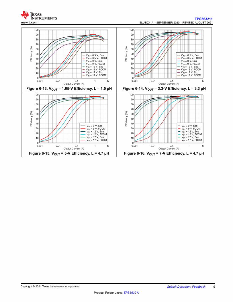
Figure 6-13. VOUT = 1.05-V Efficiency, L = 1.5 µHOutput Current (A)
Eff
icie
ncy (
%)
0.001 0.01 0.1 1 550
10
20
30
40
50
60
70
80
90
100
VIN = 6.5 V, EcoVIN = 6.5 V, FCCMVIN = 9 V, EcoVIN = 9 V, FCCMVIN = 12 V, EcoVIN = 12 V, FCCMVIN = 17 V, EcoVIN = 17 V, FCCM
Figure 6-14. VOUT = 3.3-V Efficiency, L = 3.3 µH
Output Current (A)
Eff
icie
ncy (
%)
0.001 0.01 0.1 1 550
10
20
30
40
50
60
70
80
90
100
VIN = 9 V, EcoVIN = 9 V, FCCMVIN = 12 V, EcoVIN = 12 V, FCCMVIN = 17 V, EcoVIN = 17 V, FCCM
Figure 6-15. VOUT = 5-V Efficiency, L = 4.7 µHOutput Current (A)
Eff
icie
ncy (
%)
0.001 0.01 0.1 1 550
10
20
30
40
50
60
70
80
90
100
VIN = 9 V, EcoVIN = 9 V, FCCMVIN = 12 V, EcoVIN = 12 V, FCCMVIN = 17 V, EcoVIN = 17 V, FCCM
Figure 6-16. VOUT = 7-V Efficiency, L = 4.7 µH
www.ti.comTPS563211
SLUSDX1A – SEPTEMBER 2020 – REVISED AUGUST 2021
Copyright © 2021 Texas Instruments Incorporated Submit Document Feedback 9
Product Folder Links: TPS563211
7 Detailed Description7.1 OverviewThe device is a 3-A synchronous buck converter that operates from a 4.2-V to 18-V input voltage and 0.6-V to 7-V output voltage. The device employs AECM control, an emulated current control topology that combines the advantages of peak current mode control and D-CAP2 control, providing fast transient response with true fixed switching frequency.
With the proper MODE configurations, the device supports selectable Eco-mode operation or FCCM operation and a selectable power-good indicator or external soft start.
With an on-time extension function, the device supports a maximum duty cycle of 98%.
7.2 Functional Block Diagram
Vfb
+
-gm
Vref
Vref_int
++
Error Amp
+
-
-
Comparator
+
R1
R2
R3
Crj
Vripple
Vslp
Mode Detection
Ripple Injection Generator
R
SQ
Ton Timer
PWM
PFM
Oscillator & Slope CompGenerator
FB
-
+
-
+
TSD
-
+
SW
Bootstrap
Regulator
Control LogicVCC
VCC RegulatorBias & Voltage
Reference
OVP
UVP
HS & LS Current Sense
VUVP
VOVP
Mode Selection & PG or SS Selection
UVLO
Soft-Start
VPGTH
Eco-mode or FCCM
SW
FB
PG/SS
PG or SS ?
Eco-mode or FCCM
MODE
GND
BOOT
VIN
EN
7.3 Feature Description7.3.1 Advanced Emulated Current Mode Control
The device employs AECM control, an emulated current control based topology that combines the advantages of peak current mode control and D-CAP2 control, providing fast transient response with true fixed switching frequency. The AECM control topology supports two basic regulation modes, which are PFM regulation mode and PWM regulation mode. During PWM, it operates at its nominal switching frequency in CCM or DCM. The frequency is typically about 600 kHz with a controlled frequency variation. If the load current decreases, it enters PFM to sustain high efficiency down to very light loads. In PFM, the switching frequency decreases with the load
TPS563211SLUSDX1A – SEPTEMBER 2020 – REVISED AUGUST 2021 www.ti.com
10 Submit Document Feedback Copyright © 2021 Texas Instruments Incorporated
Product Folder Links: TPS563211

current. With the internal adaptive loop adjustment, the device eliminates the need for external compensation to provide a fast transient response over a wide output voltage range.
7.3.2 Mode Selection and PG/SS Pin Function Configuration
The device requires a mode resistor to select the operations mode under light load and configure the function of pin 1. Table 7-1 shows the MODE pin settings.
Table 7-1. MODE Pin SettingsMODE RESISTOR
RANGE
RECOMMENDED MODE RESISTOR
VALUE
OPERATION MODE IN LIGHT LOAD
FUNCTION OF PG/SS PIN
[0, 12] kΩ 0 Eco-mode Power Good
[30, 50] kΩ 47 kΩ Eco-mode Soft Start
[83, 120] kΩ 100 kΩ FCCM Soft Start
[180, ∞] kΩ Float FCCM Power Good
Figure 7-1 shows the typical start-up sequence of the device once the enable signal triggers the EN turn-on threshold. After the voltage of VIN crosses the UVLO rising threshold, it takes approximately 110 μs to finish reading and setting of the MODE pin. After this process, the MODE status is latched and does not change until VIN or EN toggles to restart-up this device. Then, the soft-start function begins to ramp up the reference voltage to the PWM comparator.
PGOOD
EN
VIN
MODE
VOUT
EN threshold
1.18V
VIN
UVLO
4V
110µs 110µs
Mode
detection
Tss100µs
t
Figure 7-1. Power-Up Sequence
7.3.3 Power Good (PG)
This is an optional function configured by the MODE pin.
The device has a built-in power good (PG) function to indicate whether the output voltage has reached its appropriate level or not. The PG signal can be used for start-up sequencing of multiple rails. The PG/SS pin works as an open-drain output that requires a pullup resistor (to any voltage below 5.5 V). A pullup resistor of 10 kΩ is recommended to pull it up to a 5-V voltage. It can sink 0.8 mA of current and maintain its specified logic low level. Once the FB pin voltage is between 92% and 112% of the internal reference voltage (VREF) and after a deglitch time of 112 μs, the PG/SS is high impedance. The PG/SS pin is pulled low after a deglitch time of 48 μs when the FB pin voltage is lower than UVP or greater than OVP threshold, or in events of thermal shutdown, EN shutdown, or UVLO conditions. VIN must remain present for the PG/SS pin to stay low.
www.ti.comTPS563211
SLUSDX1A – SEPTEMBER 2020 – REVISED AUGUST 2021
Copyright © 2021 Texas Instruments Incorporated Submit Document Feedback 11
Product Folder Links: TPS563211
If the power-good output is not used when PG function is selected, it is recommended to tie to GND to get better thermal performance.
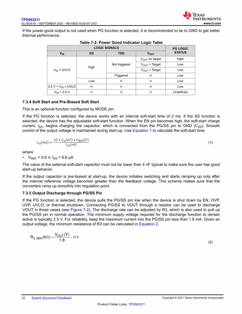
Table 7-2. Power Good Indicator Logic TableLOGIC SIGNALS PG LOGIC
STATUSVIN EN TSD VOUT
VIN > UVLOHigh
Not triggered
VOUT on target High
VOUT > Target Low
VOUT < Target Low
Triggered ✕ Low
Low ✕ ✕ Low
2.5 V < VIN < UVLO ✕ ✕ ✕ Low
VIN < 2.5 V ✕ ✕ ✕ Undefined
7.3.4 Soft Start and Pre-Biased Soft Start
This is an optional function configured by MODE pin.
If the PG function is selected, the device works with an internal soft-start time of 2 ms. If the SS function is selected, the device has the adjustable soft-start function. When the EN pin becomes high, the soft-start charge current, ISS, begins charging the capacitor, which is connected from the PG/SS pin to GND (CSS). Smooth control of the output voltage is maintained during start-up. Use Equation 1 to calculate the soft-start time.
tss ms = 3.5 × Css nF × VREF VIss uA (1)
where• VREF = 0.6 V, ISS = 6.6 µA
The value of the external soft-start capacitor must not be lower than 4 nF typical to make sure the user has good start-up behavior.
If the output capacitor is pre-biased at start-up, the device initiates switching and starts ramping up only after the internal reference voltage becomes greater than the feedback voltage. This scheme makes sure that the converters ramp up smoothly into regulation point.
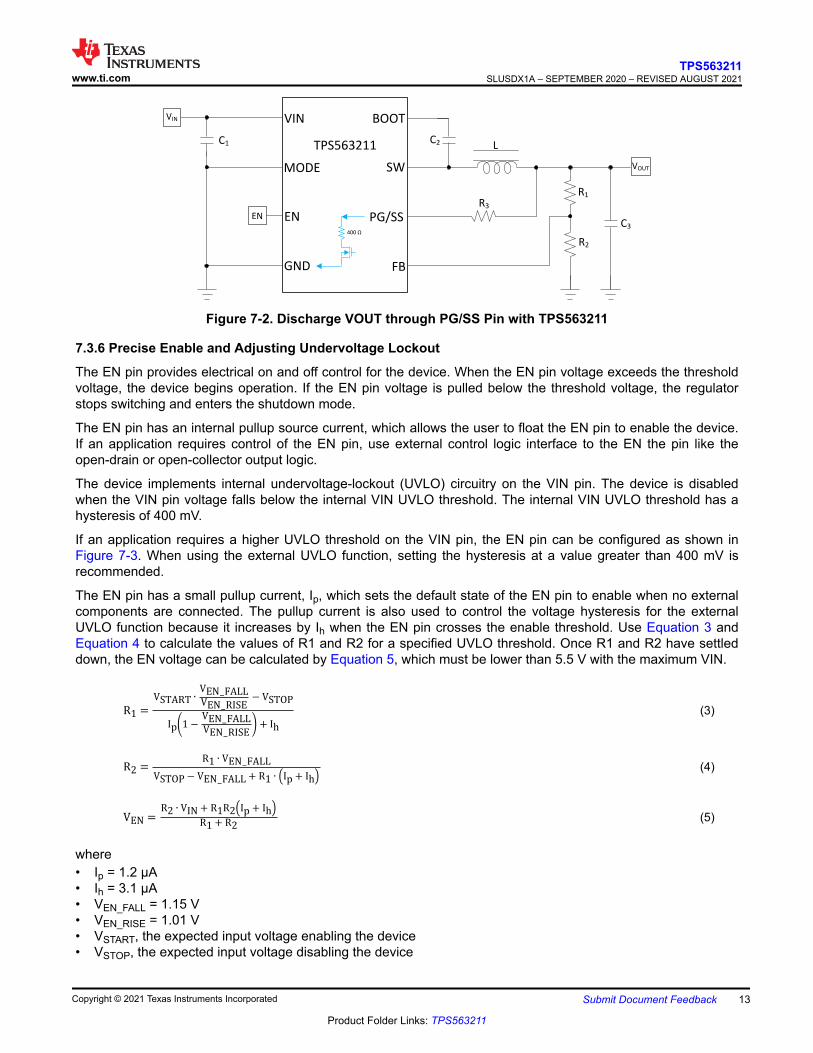
7.3.5 Output Discharge through PG/SS Pin
If the PG function is selected, the device pulls the PG/SS pin low when the device is shut down by EN, OVP, UVP, UVLO, or thermal shutdown. Connecting PG/SS to VOUT through a resistor can be used to discharge VOUT in those cases (see Figure 7-2). The discharge rate can be adjusted by R3, which is also used to pull up the PG/SS pin in normal operation. The minimum supply voltage required for the discharge function to remain active is typically 2.5 V. For reliability, keep the maximum current into the PG/SS pin less than 1.8 mA. Given an output voltage, the minimum resistance of R3 can be calculated in Equation 2.
0 4OUT
3_MIN
V (V)R (k ) .
1.8: �
(2)
TPS563211SLUSDX1A – SEPTEMBER 2020 – REVISED AUGUST 2021 www.ti.com
12 Submit Document Feedback Copyright © 2021 Texas Instruments Incorporated
Product Folder Links: TPS563211
VIN
EN
MODE
BOOT
PG/SS
SW
C1 L
R1
R2
C3
C2
GND FB
VIN
VOUT
EN
TPS563211
R3
400 Q
Figure 7-2. Discharge VOUT through PG/SS Pin with TPS563211
7.3.6 Precise Enable and Adjusting Undervoltage Lockout
The EN pin provides electrical on and off control for the device. When the EN pin voltage exceeds the threshold voltage, the device begins operation. If the EN pin voltage is pulled below the threshold voltage, the regulator stops switching and enters the shutdown mode.
The EN pin has an internal pullup source current, which allows the user to float the EN pin to enable the device. If an application requires control of the EN pin, use external control logic interface to the EN the pin like the open-drain or open-collector output logic.
The device implements internal undervoltage-lockout (UVLO) circuitry on the VIN pin. The device is disabled when the VIN pin voltage falls below the internal VIN UVLO threshold. The internal VIN UVLO threshold has a hysteresis of 400 mV.
If an application requires a higher UVLO threshold on the VIN pin, the EN pin can be configured as shown in Figure 7-3. When using the external UVLO function, setting the hysteresis at a value greater than 400 mV is recommended.
The EN pin has a small pullup current, Ip, which sets the default state of the EN pin to enable when no external components are connected. The pullup current is also used to control the voltage hysteresis for the external UVLO function because it increases by Ih when the EN pin crosses the enable threshold. Use Equation 3 and Equation 4 to calculate the values of R1 and R2 for a specified UVLO threshold. Once R1 and R2 have settled down, the EN voltage can be calculated by Equation 5, which must be lower than 5.5 V with the maximum VIN.
R1 = VSTART ∙ VEN_FALLVEN_RISE − VSTOPIp 1− VEN_FALLVEN_RISE + Ih (3)
R2 = R1 ∙ VEN_FALLVSTOP− VEN_FALL + R1 ∙ Ip + Ih (4)
VEN = R2 ∙ VIN + R1R2 Ip + IhR1 + R2 (5)
where• Ip = 1.2 µA• Ih = 3.1 µA• VEN_FALL = 1.15 V• VEN_RISE = 1.01 V• VSTART, the expected input voltage enabling the device• VSTOP, the expected input voltage disabling the device
www.ti.comTPS563211
SLUSDX1A – SEPTEMBER 2020 – REVISED AUGUST 2021
Copyright © 2021 Texas Instruments Incorporated Submit Document Feedback 13
Product Folder Links: TPS563211

EN
Ip IhR1
R2
VIN Device
Figure 7-3. Adjustable VIN Undervoltage Lockout
7.3.7 Overcurrent Limit and Undervoltage Protection
The device is protected from overcurrent conditions by cycle-by-cycle current limiting on both the peak and valley of the inductor current.
During the on time of the high-side MOSFET switch, the inductor current flows through the high-side MOSFET and increases at a linear rate determined by VIN, VOUT, the on time, and the output inductor value. The high-side switch current is sensed when the high-side MOSFET is turned on after a set of blanking time and then compared with the high-side MOSFET current limit threshold in every switching cycle. If the cross-limit event is detected after the minimum on time, the high-side MOSFET is turned off immediately. The high-side MOSFET current is limited by a clamped maximum peak current threshold IHS_LIMIT, which is constant.
The current going through low-side MOSFET is also sensed and monitored. When the low-side MOSFET is turned on, the inductor current begins ramping down. The low-side MOSFET is not turned off at the end of a switching cycle if its current is above the low-side current limit, ILS_LIMIT. The low-side MOSFET is kept on for the next cycle so that inductor current keeps ramping down, until the inductor current ramps below the low-side current limit, ILS_LIMIT, and the subsequent switching cycle comes, the low-side MOSFET is turned off and the high-side MOSFET is turned on after a dead time.
There are some important considerations for this type of overcurrent protection. The load current is higher than the overcurrent threshold by one-half of the peak-to-peak inductor ripple current. Also, when the current is being limited, the output voltage tends to fall as the demanded load current can be higher than the current available from the converter. When the VFB voltage falls below the UVP threshold voltage, the UVP comparator detects it. The device shuts down after the UVP delay time (typically 108 μs) and re-starts after the hiccup time (six times of soft-start time). The hiccup behavior helps reduce the device power dissipation under severe overcurrent conditions.
When the overcurrent condition is removed, the output voltage returns to the regulated value.
7.3.8 Overvoltage Protection
The device detects overvoltage condition by monitoring the feedback voltage. When the feedback voltage becomes higher than 112% of the target voltage, the OVP comparator output goes high and both the high-side MOSFET and low-side MOSFET turns off. This function is a non-latch operation.
7.3.9 Thermal Shutdown
The internal thermal shutdown circuitry forces the device to stop switching if the junction temperature exceeds 150°C typically. The device re-initiates the power-up sequence when the junction temperature drops below 130°C typically.
TPS563211SLUSDX1A – SEPTEMBER 2020 – REVISED AUGUST 2021 www.ti.com
14 Submit Document Feedback Copyright © 2021 Texas Instruments Incorporated
Product Folder Links: TPS563211
7.4 Device Functional Modes7.4.1 Shutdown Mode
The EN pin provides electrical on and off control for the device. When VEN is below 1.12 V (typical), the device is in Shutdown mode with a shutdown current of 3 μA (typical). The device also employs VIN UVLO protection. If VIN voltage is below their respective UVLO level, the regulator is turned off.
7.4.2 Active Mode
The device is Active mode when VEN is above the precision enable threshold voltage and VIN is above its respective UVLO level. The simplest way to enable the device is to float the EN pin. This allows self-start-up when the input voltage is in the operating range 4.2 V to 18 V.
In Active mode, depending on the load current and the configuration of MODE pin, the device is in one of the following modes:1. Continuous Conduction Mode (CCM) operation with fixed switching frequency. When load current is above
half of the peak-to-peak inductor current ripple. The device works with PWM regulation.2. Force Continuous Conduction Mode (FCCM) operation with fixed switching frequency. No matter what the
load current is, the device works with PWM regulation.3. Discontinuous Conduction Mode (DCM) operation with fixed switching frequency. When load current is
lower than half of the peak-to-peak inductor current ripple in CCM operation, the device works with PWM regulation.
4. Eco-mode operation with switching frequency decreased at very light load, the device works with PFM regulation.
7.4.3 CCM Operation
CCM operation is employed in the device when the load current is higher than half of the peak-to-peak inductor current. In CCM operation, the frequency of operation is fixed, output voltage ripple is at a minimum in this mode, and the maximum continuous output current of 3 A can be supplied by the device.
7.4.4 FCCM Operation
If FCCM operation is selected by MODE pin, the device is set to operate in FCCM operation in light load conditions and allows the inductor current to become negative. In FCCM, the device switches with a fixed frequency over the entire load range, which is suitable for applications requiring tight control of the switching frequency and output voltage ripple.
7.4.5 DCM Operation and Eco-Mode Operation
The light load running includes DCM operation and Eco-mode operation.
As the output current decreases from heavy load condition, the inductor current reduces as well and eventually comes to a point that its rippled valley touches zero level, which is the boundary between CCM and DCM. The low-side MOSFET is turned off when the zero inductor current is detected. As the load current further decreases, the converter runs into DCM.
At even lighter current loads, Eco-mode is activated to maintain high efficiency operation. The on time is kept almost the same as it was in CCM so that it takes longer time to discharge the output capacitor with smaller load current to the level of the reference voltage. This makes the switching frequency lower, proportional to the load current, and keeps the light load efficiency high. The transition point to the light load operation, IOUT(LL), current can be calculated in Equation 6.
2
1
0 85
2
IN OUT OUTOUT(LL)
sw IN
(V V ) V.I
L f V
� � �
� � (6)
7.4.6 On-Time Extension for Large Duty Cycle Operation
Minimum on time, TON_MIN, is the smallest duration of time that the high-side MOSFET can be on. TON_MIN is typically 45 ns in the device. Minimum off time, TOFF_MIN, is the smallest duration that the high-side MOSFET
www.ti.comTPS563211
SLUSDX1A – SEPTEMBER 2020 – REVISED AUGUST 2021
Copyright © 2021 Texas Instruments Incorporated Submit Document Feedback 15
Product Folder Links: TPS563211

can be off. TOFF_MIN is typically 105 ns in the device. In CCM operation, TON_MIN and TOFF_MIN limit the voltage conversion range given a fixed switching frequency.
The minimum duty cycle allowed is:
MIN ON_MIN SWD T f u
(7)
The maximum duty cycle allowed is:
1MAX OFF _MIN SWD T f � u
(8)
In the device, a frequency foldback scheme is employed to extend the maximum duty cycle when TOFF_MIN is reached. The switching frequency decreases once longer duty cycle is needed under low VIN conditions. With the duty increased, the on-time is extended until up to the maximum on-time, 6 μs. Wide range of frequency foldback allows the device output voltage stay in regulation with a much lower supply voltage VIN. This leads to a lower effective dropout voltage.
Given an output voltage, the maximum operation supply voltage can be found by:
OUTIN_MAX
SW ON_MIN
VV
f T
�
(9)
At lower supply voltage, the switching frequency decreases once TOFF_MIN is triggered. The minimum VIN without frequency foldback can be approximated by:
OUTIN_MIN
SW OFF _MIN
VV
(1-f T )
�
(10)
Taking considerations of power losses in the system with heavy load operation, VIN_MAX is higher than the result calculated in Equation 9. With frequency foldback, VIN_VIN is lowered by decreased fSW, as shown in Figure 7-4.
Sw
itch
ing
Fre
qu
en
cy (
kH
z)
4 4.25 4.5 4.75 5 5.25 5.5 5.75 6 6.25 6.5100
150
200
250
300
350
400
450
500
550
600
650
IOUT = 0.5 AIOUT = 1.5 AIOUT = 3 A
Figure 7-4. Frequency Foldback at Dropout (VOUT = 5 V)
TPS563211SLUSDX1A – SEPTEMBER 2020 – REVISED AUGUST 2021 www.ti.com
16 Submit Document Feedback Copyright © 2021 Texas Instruments Incorporated
Product Folder Links: TPS563211
8 Application and ImplementationNote
Information in the following applications sections is not part of the TI component specification, and TI does not warrant its accuracy or completeness. TI’s customers are responsible for determining suitability of components for their purposes, as well as validating and testing their design implementation to confirm system functionality.
8.1 Application InformationThe device is a highly integrated, synchronous buck converter. This device is used to convert a higher DC input voltage to a lower DC output voltage, with a maximum output current of 3 A. Alternately, the WEBENCH®
software may be used to generate a complete design. The WEBENCH software uses an iterative design procedure and accesses a comprehensive database of components when generating a design. This section presents a simplified discussion of the design process.
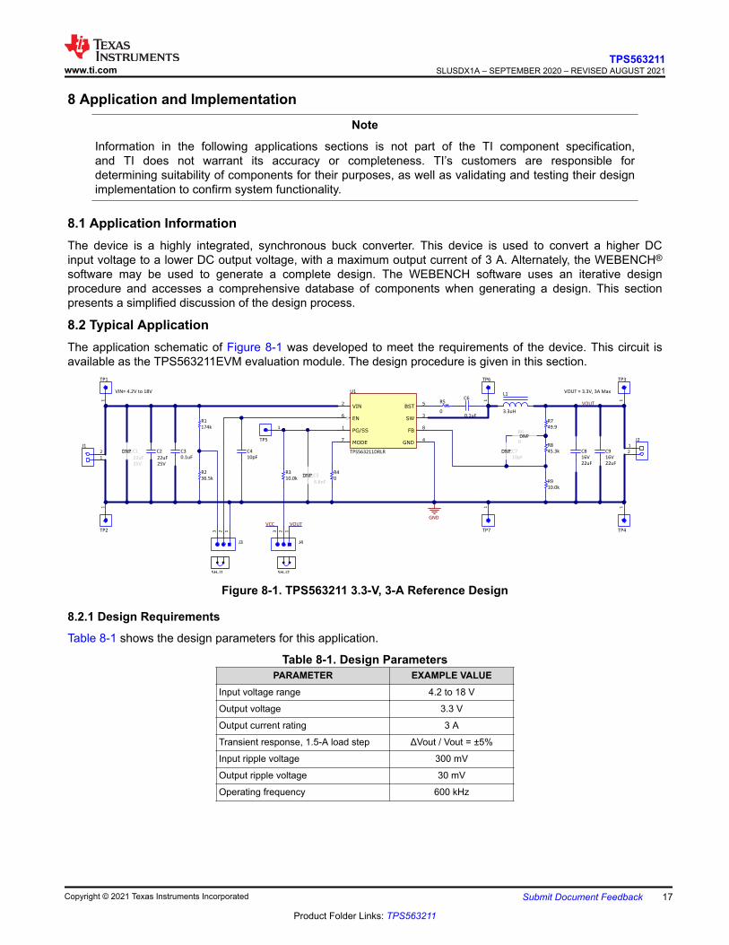
8.2 Typical ApplicationThe application schematic of Figure 8-1 was developed to meet the requirements of the device. This circuit is available as the TPS563211EVM evaluation module. The design procedure is given in this section.
VIN= 4.2V to 18V VOUT = 3.3V, 3A Max
C7
10pF
DNP
0.1uF
C6
0.1uF
C3
6.8nF
C5DNP
49.9
R7
10.0k
R9
45.3k
R8
36.5k
R2
174k
R1
25V
22uF
C1DNP
25V
22uF
C2
16V
22uF
C8
16V
22uF
C9
123
J3
123
J4
VOUTVCC
1
2
J2
GND
1
TP6
1
TP5
10.0k
R3
1
2
J1
1
TP1
1
TP2
1
TP3
1
TP4
VOUT
1
TP7
VIN2
BST5
EN6
FB8
MODE7
PG/SS1
SW3
GND4
TPS563211DRLR
U1
3.3uH
L1
0
R5
0
R4
SH-J1 SH-J2
0
R6DNP
C4
10pF
Figure 8-1. TPS563211 3.3-V, 3-A Reference Design
8.2.1 Design Requirements
Table 8-1 shows the design parameters for this application.
Table 8-1. Design ParametersPARAMETER EXAMPLE VALUE
Input voltage range 4.2 to 18 V
Output voltage 3.3 V
Output current rating 3 A
Transient response, 1.5-A load step ΔVout / Vout = ±5%
Input ripple voltage 300 mV
Output ripple voltage 30 mV
Operating frequency 600 kHz
www.ti.comTPS563211
SLUSDX1A – SEPTEMBER 2020 – REVISED AUGUST 2021
Copyright © 2021 Texas Instruments Incorporated Submit Document Feedback 17
Product Folder Links: TPS563211
8.2.2 Detailed Design Procedure8.2.2.1 Custom Design With WEBENCH® Tools
Click here to create a custom design using the TPS563211 device with the WEBENCH® Power Designer.
1. Start by entering the input voltage (VIN), output voltage (VOUT), and output current (IOUT) requirements.2. Optimize the design for key parameters such as efficiency, footprint, and cost.3. Open the advanced tab to optimize for output voltage ripple.4. Once in a TPS563211 design, you can enable the second stage L-C filter and change other settings from the
drop-down on the left.
The WEBENCH Power Designer provides a customized schematic along with a list of materials with real-time pricing and component availability.
In most cases, these actions are available:
• Run electrical simulations to see important waveforms and circuit performance• Export customized schematic and layout into popular CAD formats• Print PDF reports for the design, and share the design with colleagues
Get more information about WEBENCH tools at www.ti.com/WEBENCH.
8.2.2.2 Output Voltage Resistors Selection
The output voltage is set with a resistor divider from the output node to the FB pin. TI recommends using 1% tolerance or better divider resistors. Referring to the application schematic of Figure 8-1, start with 10 kΩ or 20 kΩ for R9 and use Equation 11 to calculate R8. To improve efficiency at light loads, consider using larger value resistors. If the values are too high, the regulator is more susceptible to noise and voltage errors from the FB input current are noticeable.
8 9
OUT REF
REF
V VR R
V
� �
(11)
Table 8-2 shows the recommended components value for common output voltages.
8.2.2.3 Output Inductor Selection
To calculate the minimum value of the output inductor, use Equation 12. KIND is a coefficient that represents the amount of inductor ripple current relative to the maximum output current. The inductor ripple current is filtered by the output capacitor. Therefore, choosing high inductor ripple currents impact the selection of the output capacitor because the output capacitor must have a ripple current rating equal to or greater than the inductor ripple current. In general, the inductor ripple value is at the discretion of the designer. For this part, TI recommends the range of KIND from 25% to 55%.
IN_MAX OUTOUTMIN
IN_MAX IND OUT SW
V VVL
V K I f
�
�
� �
(12)
where• IOUT = 3 A
For this design example, use KIND = 50%. The inductor value is calculated to be 2.99 μH. For this design, a nearest standard value was chosen: 3.3 μH. For the output filter inductor, it is important that the RMS current and saturation current ratings not be exceeded. The inductor peak-to-peak ripple current, peak current, and RMS current are calculated using Equation 13, Equation 14, and Equation 15.
TPS563211SLUSDX1A – SEPTEMBER 2020 – REVISED AUGUST 2021 www.ti.com
18 Submit Document Feedback Copyright © 2021 Texas Instruments Incorporated
Product Folder Links: TPS563211
1
IN_MAX OUTOUTRIPPLE
IN_MAX SW
V VVI
V L f
�
�
�
(13)
2
RIPPLELPEAK OUT
II I �
(14)
2 21
12LRMS OUT RIPPLEI I I �
(15)
For this design example, the calculated peak current is 3.68 A and the calculated RMS current is 3.02 A. The chosen inductor is a Wurth Elektronik 74437349033 3.3-μH. It has a saturation current rating of 12 A and a RMS current rating of 6 A.
The current flowing through the inductor is the inductor ripple current plus the output current. During power up, faults, or transient load conditions, the inductor current can increase above the calculated peak inductor current level calculated above. In transient conditions, the inductor current can increase up to the switch current limit of the device. For this reason, the most conservative approach is to specify an inductor with a saturation current rating equal to or greater than the switch current limit rather than the peak inductor current.
8.2.2.4 Output Capacitor Selection
After selecting the inductor, the output capacitor needs to be optimized. The LC filter used as the output filter has double pole at:
1
1
2P
OUT _E
fL C
S �
(16)
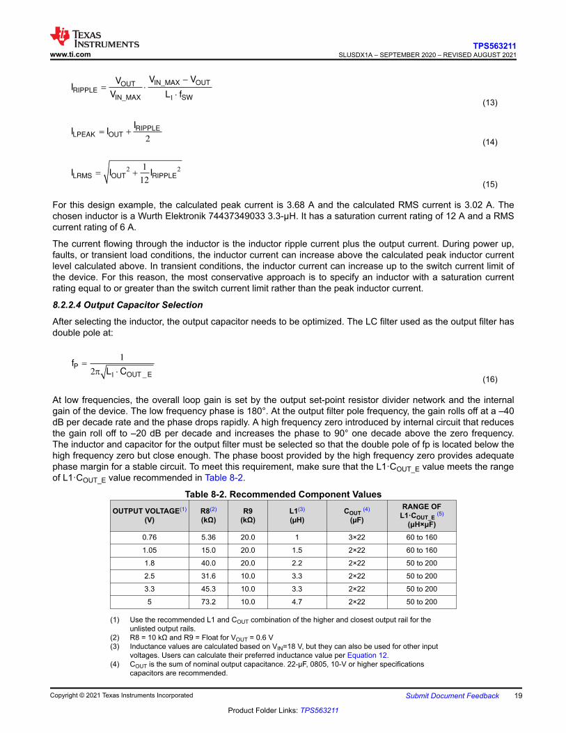
At low frequencies, the overall loop gain is set by the output set-point resistor divider network and the internal gain of the device. The low frequency phase is 180°. At the output filter pole frequency, the gain rolls off at a –40 dB per decade rate and the phase drops rapidly. A high frequency zero introduced by internal circuit that reduces the gain roll off to –20 dB per decade and increases the phase to 90° one decade above the zero frequency. The inductor and capacitor for the output filter must be selected so that the double pole of fp is located below the high frequency zero but close enough. The phase boost provided by the high frequency zero provides adequate phase margin for a stable circuit. To meet this requirement, make sure that the L1·COUT_E value meets the range of L1·COUT_E value recommended in Table 8-2.
Table 8-2. Recommended Component ValuesOUTPUT VOLTAGE(1)
(V)R8(2)
(kΩ)R9
(kΩ)L1(3)
(µH)COUT (4)
(µF)
RANGE OF L1·COUT_E (5)
(μH×μF)0.76 5.36 20.0 1 3×22 60 to 160
1.05 15.0 20.0 1.5 2×22 60 to 160
1.8 40.0 20.0 2.2 2×22 50 to 200
2.5 31.6 10.0 3.3 2×22 50 to 200
3.3 45.3 10.0 3.3 2×22 50 to 200
5 73.2 10.0 4.7 2×22 50 to 200
(1) Use the recommended L1 and COUT combination of the higher and closest output rail for the unlisted output rails.
(2) R8 = 10 kΩ and R9 = Float for VOUT = 0.6 V(3) Inductance values are calculated based on VIN=18 V, but they can also be used for other input
voltages. Users can calculate their preferred inductance value per Equation 12.(4) COUT is the sum of nominal output capacitance. 22-μF, 0805, 10-V or higher specifications
capacitors are recommended.
www.ti.comTPS563211
SLUSDX1A – SEPTEMBER 2020 – REVISED AUGUST 2021
Copyright © 2021 Texas Instruments Incorporated Submit Document Feedback 19
Product Folder Links: TPS563211

(5) COUT_E is the effective value after derating. The value of L1·COUT_E must be within in the range.
The capacitor value and ESR determines the amount of output voltage ripple. The device is intended for use with ceramic or other low-ESR capacitors. Use Equation 17 to determine the required RMS current rating for the output capacitor.
12
OUT IN_MAX OUTCORMS
IN_MAX 1 SW
V (V V )I
V L f
� �
� � �
(17)
Two Murata GRM21BR61C226ME44L 22-μF, 0805, 16-V output capacitors are used for this design. From the data sheet, the estimated DC derating rate is 66.8% at room temperature with AC voltage of 0.2 V. The total output effective capacitance is approximately 29.4 μF. The value of L1·COUT_E is 97 μH×μF, which is within the recommended range.
8.2.2.5 Input Capacitor Selection
The device requires an input decoupling capacitor. A bulk capacitor is needed depending on the application. TI recommends a ceramic capacitor over 10 μF for the decoupling capacitor. An additional 0.1-μF capacitor (C3) from VIN pin to ground is recommended to provide additional high frequency filtering. The capacitor voltage rating needs to be greater than the maximum input voltage. The capacitor must also have a ripple current rating greater than the maximum input current ripple of the device. The input ripple current can be calculated using Equation 18.
IN_MIN OUTOUTCIRMS OUT
IN_MIN IN_MIN
V VVI I
V V
�
� �
(18)
The value of a ceramic capacitor varies significantly over temperature and the amount of DC bias applied to the capacitor. The capacitance variations due to temperature can be minimized by selecting a dielectric material that is stable over temperature. X5R and X7R ceramic dielectrics are usually selected for power regulator capacitors because they have a high capacitance-to-volume ratio and are fairly stable over temperature. The output capacitor must also be selected with the DC bias taken into account. The capacitance value of a capacitor decreases as the DC bias across a capacitor increases. For this example design, a ceramic capacitor with at least a 25-V voltage rating is required to support the maximum input voltage. For this design, one Murata GRM21BR61E226ME44L (10-μF, 25-V, 0805, X5R) capacitor has been selected. The effective capacitance under input voltage of 12 V is 0.18 × 22 = 4 μF. The input capacitance value determines the input ripple voltage of the regulator. The input voltage ripple can be calculated using Equation 19. Using the design example values, IOUT_MAX = 3 A, CIN_E = 4 μF, fSW = 600 kHz, yields an input voltage ripple of 313 mV and a RMS input ripple current of 1.23 A.
0 25OUT _MAXIN OUT _MAX ESR _MAX
IN SW
I .V (I R )
C f
�' � �
�(19)
where• RESR_MAX = the maximum series resistance of the input capacitor
8.2.2.6 Bootstrap Capacitor Selection
A 0.1-μF ceramic capacitor must be connected between the BOOT to SW pin for proper operation. TI recommends to use a ceramic capacitor with X5R or better grade dielectric. The capacitor must have a 10-V or higher voltage rating.
8.2.2.7 Undervoltage Lockout Set Point
The undervoltage lockout (UVLO) can be adjusted using the external voltage divider network of R1 and R2. R1 is connected between VIN and the EN pin of the TPS563211 and R2 is connected between EN and GND.
TPS563211SLUSDX1A – SEPTEMBER 2020 – REVISED AUGUST 2021 www.ti.com
20 Submit Document Feedback Copyright © 2021 Texas Instruments Incorporated
Product Folder Links: TPS563211
The UVLO has two thresholds, one for power up when the input voltage is rising and one for power down or brownouts when the input voltage is falling. For the example design, the supply should turn on and start switching when the input voltage increases above 6.6 V (UVLO start or enable). After the regulator starts switching, it must continue to do so until the input voltage falls below 5.7 V (UVLO stop or disable). Equation 3 and Equation 4 can be used to calculate the values for the upper and lower resistor values. For the stop voltages specified, the nearest standard resistor value for R1 is 174 kΩ and for R2 is 36.5 kΩ.
www.ti.comTPS563211
SLUSDX1A – SEPTEMBER 2020 – REVISED AUGUST 2021
Copyright © 2021 Texas Instruments Incorporated Submit Document Feedback 21
Product Folder Links: TPS563211
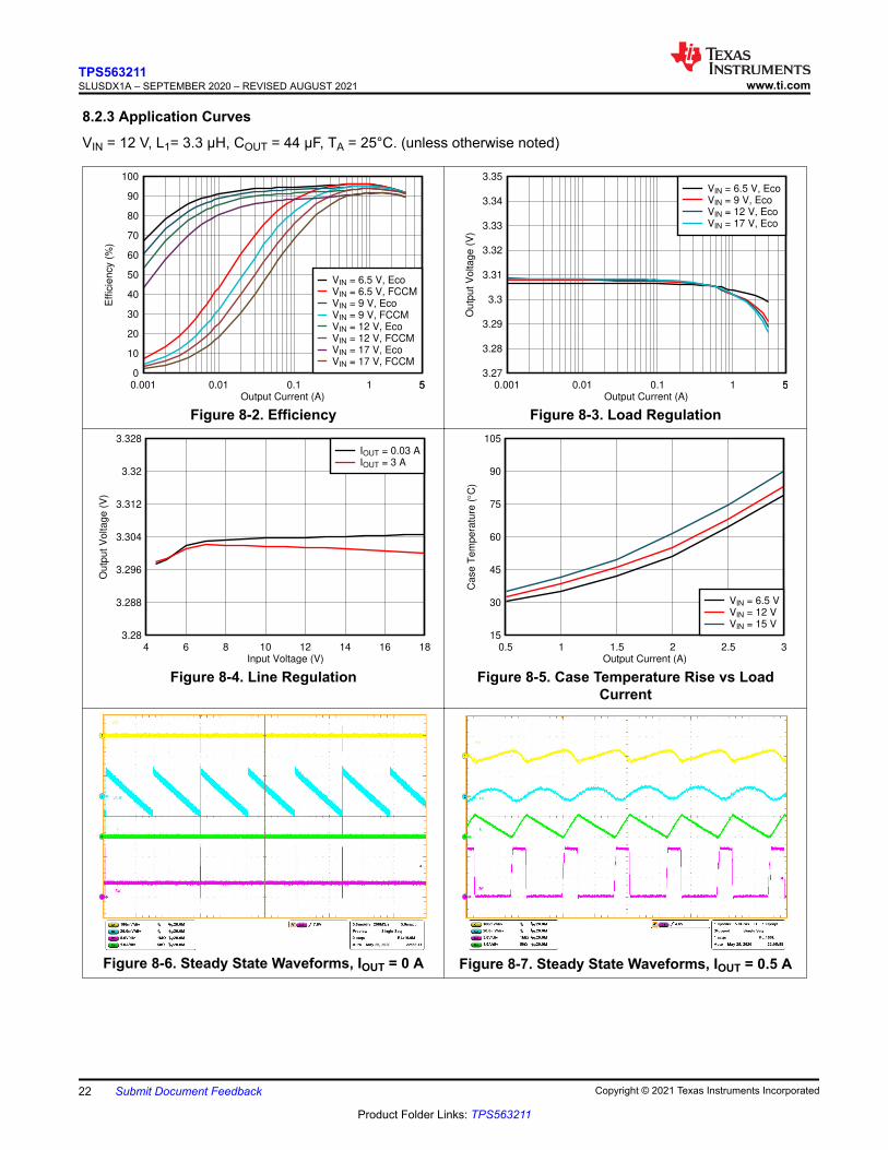
8.2.3 Application Curves
VIN = 12 V, L1= 3.3 μH, COUT = 44 μF, TA = 25°C. (unless otherwise noted)
Output Current (A)
Eff
icie
ncy (
%)
0.001 0.01 0.1 1 550
10
20
30
40
50
60
70
80
90
100
VIN = 6.5 V, EcoVIN = 6.5 V, FCCMVIN = 9 V, EcoVIN = 9 V, FCCMVIN = 12 V, EcoVIN = 12 V, FCCMVIN = 17 V, EcoVIN = 17 V, FCCM
Figure 8-2. Efficiency Output Current (A)
Ou
tpu
t V
olta
ge
(V
)
0.001 0.01 0.1 1 553.27
3.28
3.29
3.3
3.31
3.32
3.33
3.34
3.35VIN = 6.5 V, EcoVIN = 9 V, EcoVIN = 12 V, EcoVIN = 17 V, Eco
Figure 8-3. Load Regulation
Input Voltage (V)
Ou
tpu
t V
olta
ge
(V
)
4 6 8 10 12 14 16 183.28
3.288
3.296
3.304
3.312
3.32
3.328IOUT = 0.03 AIOUT = 3 A
Figure 8-4. Line RegulationOutput Current (A)
Ca
se
Te
mp
era
ture
(qC
)
0.5 1 1.5 2 2.5 315
30
45
60
75
90
105
VIN = 6.5 VVIN = 12 VVIN = 15 V
Figure 8-5. Case Temperature Rise vs Load Current
Figure 8-6. Steady State Waveforms, IOUT = 0 A Figure 8-7. Steady State Waveforms, IOUT = 0.5 A
TPS563211SLUSDX1A – SEPTEMBER 2020 – REVISED AUGUST 2021 www.ti.com
22 Submit Document Feedback Copyright © 2021 Texas Instruments Incorporated
Product Folder Links: TPS563211
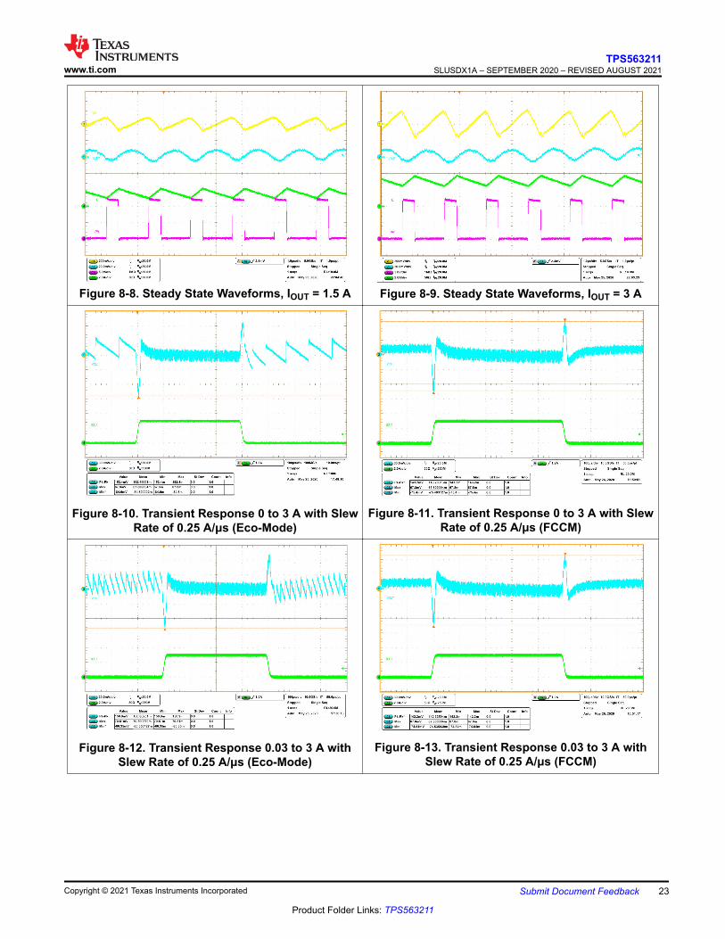
Figure 8-8. Steady State Waveforms, IOUT = 1.5 A Figure 8-9. Steady State Waveforms, IOUT = 3 A
Figure 8-10. Transient Response 0 to 3 A with Slew Rate of 0.25 A/μs (Eco-Mode)
Figure 8-11. Transient Response 0 to 3 A with Slew Rate of 0.25 A/μs (FCCM)
Figure 8-12. Transient Response 0.03 to 3 A with Slew Rate of 0.25 A/μs (Eco-Mode)
Figure 8-13. Transient Response 0.03 to 3 A with Slew Rate of 0.25 A/μs (FCCM)
www.ti.comTPS563211
SLUSDX1A – SEPTEMBER 2020 – REVISED AUGUST 2021
Copyright © 2021 Texas Instruments Incorporated Submit Document Feedback 23
Product Folder Links: TPS563211
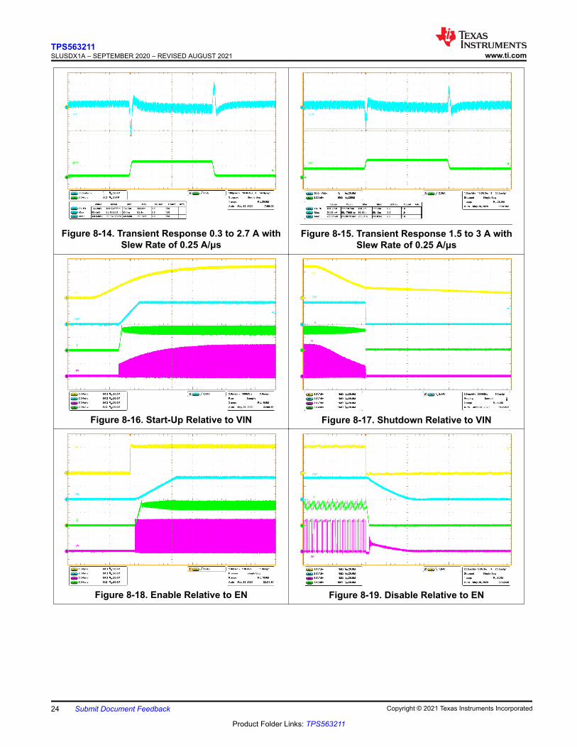
Figure 8-14. Transient Response 0.3 to 2.7 A with Slew Rate of 0.25 A/μs
Figure 8-15. Transient Response 1.5 to 3 A with Slew Rate of 0.25 A/μs
Figure 8-16. Start-Up Relative to VIN Figure 8-17. Shutdown Relative to VIN
Figure 8-18. Enable Relative to EN Figure 8-19. Disable Relative to EN
TPS563211SLUSDX1A – SEPTEMBER 2020 – REVISED AUGUST 2021 www.ti.com
24 Submit Document Feedback Copyright © 2021 Texas Instruments Incorporated
Product Folder Links: TPS563211

Figure 8-20. Output Short Protection Figure 8-21. Output Short Recovery
www.ti.comTPS563211
SLUSDX1A – SEPTEMBER 2020 – REVISED AUGUST 2021
Copyright © 2021 Texas Instruments Incorporated Submit Document Feedback 25
Product Folder Links: TPS563211
9 Power Supply RecommendationsThe devices are designed to operate from an input voltage supply range between 4.2 V and 18 V. This input supply must be well regulated. If the input supply is located more than a few inches from the device or converter, additional bulk capacitance can be required in addition to the ceramic bypass capacitors. An electrolytic capacitor with a value of 47 μF is a typical choice.
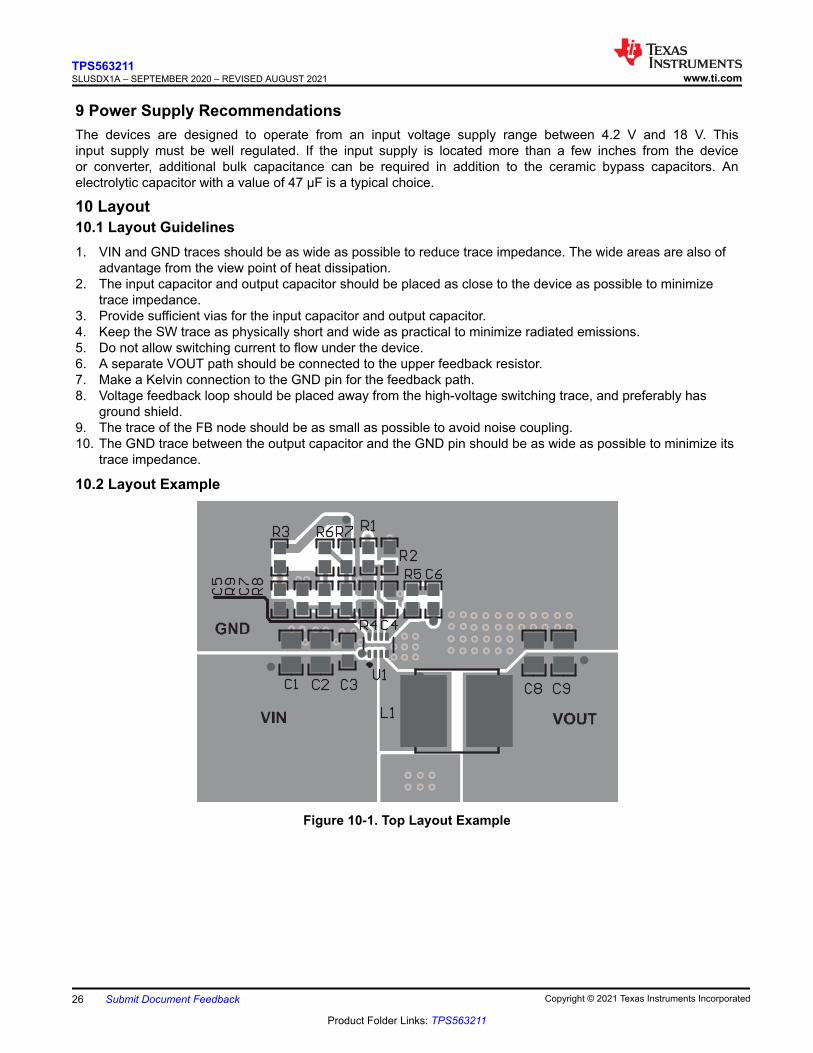
10 Layout10.1 Layout Guidelines1. VIN and GND traces should be as wide as possible to reduce trace impedance. The wide areas are also of
advantage from the view point of heat dissipation.2. The input capacitor and output capacitor should be placed as close to the device as possible to minimize
trace impedance.3. Provide sufficient vias for the input capacitor and output capacitor.4. Keep the SW trace as physically short and wide as practical to minimize radiated emissions.5. Do not allow switching current to flow under the device.6. A separate VOUT path should be connected to the upper feedback resistor.7. Make a Kelvin connection to the GND pin for the feedback path.8. Voltage feedback loop should be placed away from the high-voltage switching trace, and preferably has
ground shield.9. The trace of the FB node should be as small as possible to avoid noise coupling.10. The GND trace between the output capacitor and the GND pin should be as wide as possible to minimize its
trace impedance.
10.2 Layout Example
Figure 10-1. Top Layout Example
TPS563211SLUSDX1A – SEPTEMBER 2020 – REVISED AUGUST 2021 www.ti.com
26 Submit Document Feedback Copyright © 2021 Texas Instruments Incorporated
Product Folder Links: TPS563211

Figure 10-2. Bottom Layout Example
www.ti.comTPS563211
SLUSDX1A – SEPTEMBER 2020 – REVISED AUGUST 2021
Copyright © 2021 Texas Instruments Incorporated Submit Document Feedback 27
Product Folder Links: TPS563211
11 Device and Documentation Support11.1 Device Support11.1.1 Development Support11.1.1.1 Custom Design With WEBENCH® Tools
Click here to create a custom design using the TPS563211 device with the WEBENCH® Power Designer.
1. Start by entering the input voltage (VIN), output voltage (VOUT), and output current (IOUT) requirements.2. Optimize the design for key parameters such as efficiency, footprint, and cost.3. Open the advanced tab to optimize for output voltage ripple.4. Once in a TPS563211 design, you can enable the second stage L-C filter and change other settings from the
drop-down on the left.
The WEBENCH Power Designer provides a customized schematic along with a list of materials with real-time pricing and component availability.
In most cases, these actions are available:
• Run electrical simulations to see important waveforms and circuit performance• Export customized schematic and layout into popular CAD formats• Print PDF reports for the design, and share the design with colleagues
Get more information about WEBENCH tools at www.ti.com/WEBENCH.
11.2 Receiving Notification of Documentation UpdatesTo receive notification of documentation updates, navigate to the device product folder on ti.com. Click on Subscribe to updates to register and receive a weekly digest of any product information that has changed. For change details, review the revision history included in any revised document.
11.3 Support ResourcesTI E2E™ support forums are an engineer's go-to source for fast, verified answers and design help — straight from the experts. Search existing answers or ask your own question to get the quick design help you need.
Linked content is provided "AS IS" by the respective contributors. They do not constitute TI specifications and do not necessarily reflect TI's views; see TI's Terms of Use.
11.4 TrademarksTI E2E™ is a trademark of Texas Instruments.WEBENCH® is a registered trademark of Texas Instruments.All trademarks are the property of their respective owners.11.5 Electrostatic Discharge Caution
This integrated circuit can be damaged by ESD. Texas Instruments recommends that all integrated circuits be handled with appropriate precautions. Failure to observe proper handling and installation procedures can cause damage.ESD damage can range from subtle performance degradation to complete device failure. Precision integrated circuits may be more susceptible to damage because very small parametric changes could cause the device not to meet its published specifications.
11.6 GlossaryTI Glossary This glossary lists and explains terms, acronyms, and definitions.
TPS563211SLUSDX1A – SEPTEMBER 2020 – REVISED AUGUST 2021 www.ti.com
28 Submit Document Feedback Copyright © 2021 Texas Instruments Incorporated
Product Folder Links: TPS563211
12 Mechanical, Packaging, and Orderable InformationThe following pages include mechanical, packaging, and orderable information. This information is the most current data available for the designated devices. This data is subject to change without notice and revision of this document. For browser-based versions of this data sheet, refer to the left-hand navigation.
www.ti.comTPS563211
SLUSDX1A – SEPTEMBER 2020 – REVISED AUGUST 2021
Copyright © 2021 Texas Instruments Incorporated Submit Document Feedback 29
Product Folder Links: TPS563211
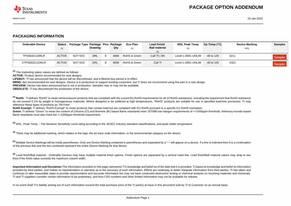
PACKAGE OPTION ADDENDUM
www.ti.com 15-Jan-2022
Addendum-Page 1
PACKAGING INFORMATION
Orderable Device Status(1)
Package Type PackageDrawing
Pins PackageQty
Eco Plan(2)
Lead finish/Ball material
(6)
MSL Peak Temp(3)
Op Temp (°C) Device Marking(4/5)
Samples
TPS563211DRLR ACTIVE SOT-5X3 DRL 8 4000 RoHS & Green Call TI | SN Level-1-260C-UNLIM -40 to 125 3211
XTPS563211DRLR ACTIVE SOT-5X3 DRL 8 4000 RoHS & Green Call TI Level-1-260C-UNLIM -40 to 125 X321
(1) The marketing status values are defined as follows:ACTIVE: Product device recommended for new designs.LIFEBUY: TI has announced that the device will be discontinued, and a lifetime-buy period is in effect.NRND: Not recommended for new designs. Device is in production to support existing customers, but TI does not recommend using this part in a new design.PREVIEW: Device has been announced but is not in production. Samples may or may not be available.OBSOLETE: TI has discontinued the production of the device.
(2) RoHS: TI defines "RoHS" to mean semiconductor products that are compliant with the current EU RoHS requirements for all 10 RoHS substances, including the requirement that RoHS substancedo not exceed 0.1% by weight in homogeneous materials. Where designed to be soldered at high temperatures, "RoHS" products are suitable for use in specified lead-free processes. TI mayreference these types of products as "Pb-Free".RoHS Exempt: TI defines "RoHS Exempt" to mean products that contain lead but are compliant with EU RoHS pursuant to a specific EU RoHS exemption.Green: TI defines "Green" to mean the content of Chlorine (Cl) and Bromine (Br) based flame retardants meet JS709B low halogen requirements of <=1000ppm threshold. Antimony trioxide basedflame retardants must also meet the <=1000ppm threshold requirement.
(3) MSL, Peak Temp. - The Moisture Sensitivity Level rating according to the JEDEC industry standard classifications, and peak solder temperature.
(4) There may be additional marking, which relates to the logo, the lot trace code information, or the environmental category on the device.
(5) Multiple Device Markings will be inside parentheses. Only one Device Marking contained in parentheses and separated by a "~" will appear on a device. If a line is indented then it is a continuationof the previous line and the two combined represent the entire Device Marking for that device.
(6) Lead finish/Ball material - Orderable Devices may have multiple material finish options. Finish options are separated by a vertical ruled line. Lead finish/Ball material values may wrap to twolines if the finish value exceeds the maximum column width.
Important Information and Disclaimer:The information provided on this page represents TI's knowledge and belief as of the date that it is provided. TI bases its knowledge and belief on informationprovided by third parties, and makes no representation or warranty as to the accuracy of such information. Efforts are underway to better integrate information from third parties. TI has taken andcontinues to take reasonable steps to provide representative and accurate information but may not have conducted destructive testing or chemical analysis on incoming materials and chemicals.TI and TI suppliers consider certain information to be proprietary, and thus CAS numbers and other limited information may not be available for release.
In no event shall TI's liability arising out of such information exceed the total purchase price of the TI part(s) at issue in this document sold by TI to Customer on an annual basis.

PACKAGE OPTION ADDENDUM
www.ti.com 15-Jan-2022
Addendum-Page 2
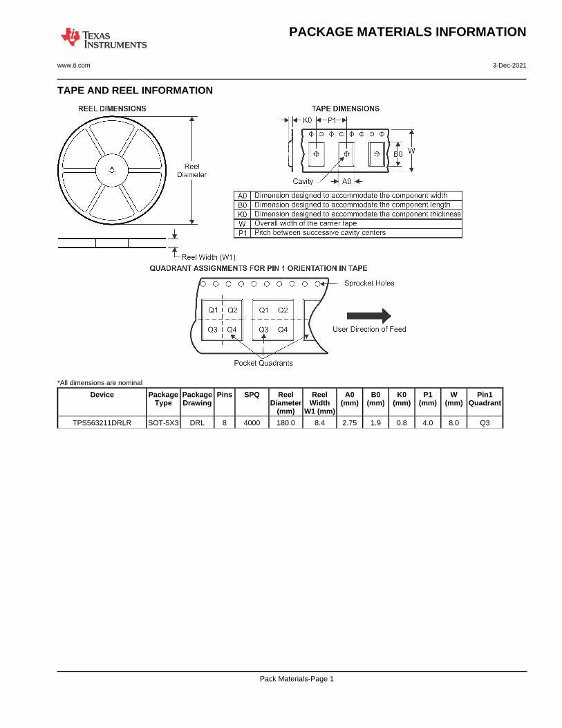
TAPE AND REEL INFORMATION
*All dimensions are nominal
Device PackageType
PackageDrawing
Pins SPQ ReelDiameter
(mm)
ReelWidth
W1 (mm)
A0(mm)
B0(mm)
K0(mm)
P1(mm)
W(mm)
Pin1Quadrant
TPS563211DRLR SOT-5X3 DRL 8 4000 180.0 8.4 2.75 1.9 0.8 4.0 8.0 Q3
PACKAGE MATERIALS INFORMATION
www.ti.com 3-Dec-2021
Pack Materials-Page 1

*All dimensions are nominal
Device Package Type Package Drawing Pins SPQ Length (mm) Width (mm) Height (mm)
TPS563211DRLR SOT-5X3 DRL 8 4000 210.0 185.0 35.0
PACKAGE MATERIALS INFORMATION
www.ti.com 3-Dec-2021
Pack Materials-Page 2

www.ti.com
PACKAGE OUTLINE
C
1.71.5
6X 0.5
2X 1.5
0.6 MAX
0.180.08
8X 0.40.2
0.050.00
8X 0.270.17
B 1.31.1
A
2.22.0
NOTE 3
SOT-5X3 - 0.6 mm max heightDRL0008APLASTIC SMALL OUTLINE
4224486/D 11/2021
NOTES: 1. All linear dimensions are in millimeters. Any dimensions in parenthesis are for reference only. Dimensioning and tolerancing per ASME Y14.5M.2. This drawing is subject to change without notice.3. This dimension does not include mold flash, protrusions, or gate burrs. Mold flash, interlead flash, protrusions, or gate burrs shall not exceed 0.15 mm per side.4.Reference JEDEC Registration MO-293, Variation UDAD
18
ID AREAPIN 1
45
SEATING PLANE
0.05 C
SCALE 8.000
0.1 C A B0.05
SYMM
SYMM

www.ti.com
EXAMPLE BOARD LAYOUT
0.05 MAXAROUND
0.05 MINAROUND
8X (0.67)
8X (0.3)
(1.48)
6X (0.5)
(R0.05) TYP
4224486/D 11/2021
SOT-5X3 - 0.6 mm max heightDRL0008APLASTIC SMALL OUTLINE
NOTES: (continued) 5. Publication IPC-7351 may have alternate designs. 6. Solder mask tolerances between and around signal pads can vary based on board fabrication site.
SYMM
LAND PATTERN EXAMPLEEXPOSED METAL SHOWN
SCALE:30X
SYMM
1
45
8
SOLDER MASKOPENING
METAL UNDERSOLDER MASK
SOLDER MASKDEFINED
EXPOSEDMETAL
METALSOLDER MASKOPENING
NON SOLDER MASKDEFINED
(PREFERRED)
SOLDERMASK DETAILS
EXPOSEDMETAL
www.ti.com
EXAMPLE STENCIL DESIGN
(1.48)
6X (0.5)
8X (0.67)
8X (0.3)
(R0.05) TYP
SOT-5X3 - 0.6 mm max heightDRL0008APLASTIC SMALL OUTLINE
4224486/D 11/2021
NOTES: (continued) 7. Laser cutting apertures with trapezoidal walls and rounded corners may offer better paste release. IPC-7525 may have alternate design recommendations. 8. Board assembly site may have different recommendations for stencil design.
SOLDER PASTE EXAMPLEBASED ON 0.1 mm THICK STENCIL
SCALE:30X
SYMM
SYMM
1
45
8

IMPORTANT NOTICE AND DISCLAIMERTI PROVIDES TECHNICAL AND RELIABILITY DATA (INCLUDING DATA SHEETS), DESIGN RESOURCES (INCLUDING REFERENCE DESIGNS), APPLICATION OR OTHER DESIGN ADVICE, WEB TOOLS, SAFETY INFORMATION, AND OTHER RESOURCES “AS IS” AND WITH ALL FAULTS, AND DISCLAIMS ALL WARRANTIES, EXPRESS AND IMPLIED, INCLUDING WITHOUT LIMITATION ANY IMPLIED WARRANTIES OF MERCHANTABILITY, FITNESS FOR A PARTICULAR PURPOSE OR NON-INFRINGEMENT OF THIRD PARTY INTELLECTUAL PROPERTY RIGHTS.These resources are intended for skilled developers designing with TI products. You are solely responsible for (1) selecting the appropriate TI products for your application, (2) designing, validating and testing your application, and (3) ensuring your application meets applicable standards, and any other safety, security, regulatory or other requirements.These resources are subject to change without notice. TI grants you permission to use these resources only for development of an application that uses the TI products described in the resource. Other reproduction and display of these resources is prohibited. No license is granted to any other TI intellectual property right or to any third party intellectual property right. TI disclaims responsibility for, and you will fully indemnify TI and its representatives against, any claims, damages, costs, losses, and liabilities arising out of your use of these resources.TI’s products are provided subject to TI’s Terms of Sale or other applicable terms available either on ti.com or provided in conjunction with such TI products. TI’s provision of these resources does not expand or otherwise alter TI’s applicable warranties or warranty disclaimers for TI products.TI objects to and rejects any additional or different terms you may have proposed. IMPORTANT NOTICE
Mailing Address: Texas Instruments, Post Office Box 655303, Dallas, Texas 75265Copyright © 2022, Texas Instruments Incorporated