Embed Size (px)
Citation preview
0
10
20
30
40
50
60
70
80
90
100
0.001 0.010 0.100
Eff
icie
ncy
(%
)
Load Current (A)
V = 12 VIN
V = 5 V, = 50 kHzOUT SWf
V = 5 V, = 400 kHz
V = 3.3 V, = 400 kHz
OUT SW
OUT SW
f
f
VOUT
BOOT
EN
VIN VIN
RT /CLK
PowerPAD
VIN
PH
VSNS
GND
VIN
TPS54061
COMP
Product
Folder
Sample &Buy
Technical
Documents
Tools &
Software
Support &Community
TPS54061SLVSBB7E –MAY 2012–REVISED NOVEMBER 2015
TPS54061 Wide Input 60-V, 200-mA Synchronous Step-Down DC-DCConverter With Low IQ
1 Features 3 DescriptionThe TPS54061 device is a 60-V, 200-mA,
1• Integrated High-Side and Low-Side MOSFETsynchronous step-down DC-DC converter with• Diode Emulation for Improved Light Load integrated high-side and low-side MOSFETs. Current
Efficiency mode control provides simple external compensation• Peak Current Mode Control and flexible component selection. The non-switching
supply current is 90 µA. Using the enable pin,• 90-µA Operating Quiescent Currentshutdown supply current is reduced to 1.4 µA.• 1.4-µA Shutdown Supply CurrentTo increase light load efficiency the low-side• 50-kHz to 1100-kHz Adjustable SwitchingMOSFET emulates a diode when the inductor currentFrequencyreaches zero.
• Synchronizes to External ClockUnder voltage lockout is internally set at 4.5 V, but• Internal Slow-Start can be increased using two resistors on the enable
• 0.8 V ±1% Voltage Reference pin. The output voltage startup ramp is controlled by• Stable With Ceramic Output Capacitors or Low- the internal slow-start time.
Cost Aluminum Electrolytic The adjustable switching frequency range allows• Cycle-by-Cycle Current Limit, Thermal, OVP and efficiency and external component size to be
Frequency Foldback Protection optimized. Frequency foldback and thermal shutdownprotects the part during an overload condition.• VSON-8 Package, 3 mm × 3 mm With Thermal
Pad The TPS54061 enables small designs by integratingthe MOSFETs, boot recharge diode, and minimizing• –40°C to 150°C Operating Junction Temperaturethe IC footprint with a small 3.00 mm x 3.00 mmthermally enhanced VSON package2 ApplicationsThe TPS54061 is supported in the WEBENCH™• 4 to 20-mA Current-Loop Powered SensorsDesigner at www.ti.com.• Low Power Standby or Bias Voltage Supplies
• Industrial Process Control, Metering, and Security Device Information(1)
Systems PART NUMBER PACKAGE BODY SIZE (NOM)• High Efficiency Replacement for High Voltage TPS54061 VSON (8) 3.00 mm x 3.00 mm
Linear Regulators(1) For all available packages, see the orderable addendum at
the end of the datasheet.
Simplified Schematic Efficiency vs Load Current
1
An IMPORTANT NOTICE at the end of this data sheet addresses availability, warranty, changes, use in safety-critical applications,intellectual property matters and other important disclaimers. PRODUCTION DATA.
TPS54061SLVSBB7E –MAY 2012–REVISED NOVEMBER 2015 www.ti.com
Table of Contents7.3 Feature Description................................................. 111 Features .................................................................. 17.4 Device Functional Modes........................................ 152 Applications ........................................................... 1
8 Application and Implementation ........................ 163 Description ............................................................. 18.1 Application Information............................................ 164 Revision History..................................................... 28.2 Typical Applications ................................................ 165 Pin Configuration and Functions ......................... 3
9 Power Supply Recommendations ...................... 306 Specifications......................................................... 410 Layout................................................................... 306.1 Absolute Maximum Ratings ...................................... 4
10.1 Layout Guidelines ................................................. 306.2 ESD Ratings.............................................................. 410.2 Layout Example .................................................... 306.3 Recommended Operating Conditions....................... 4
11 Device and Documentation Support ................. 316.4 Thermal Information .................................................. 411.1 Trademarks ........................................................... 316.5 Electrical Characteristics .......................................... 511.2 Electrostatic Discharge Caution............................ 316.6 Typical Characteristics .............................................. 711.3 Glossary ................................................................ 317 Detailed Description ............................................ 10
12 Mechanical, Packaging, and Orderable7.1 Overview ................................................................. 10Information ........................................................... 317.2 Functional Block Diagram ....................................... 11
4 Revision HistoryNOTE: Page numbers for previous revisions may differ from page numbers in the current version.
Changes from Revision D (December 2014) to Revision E Page
• Changed PH, 10ns Transient MIN value in the Absolute Maximum Ratings From: –2 V To: –4 V ....................................... 4• Moved Storage temperature, Tstg From: ESD Ratings To: Absolute Maximum Ratings. ....................................................... 4• Changed Handling Ratings table To: ESD Ratings table ....................................................................................................... 4
Changes from Revision C (September 2013) to Revision D Page
• Added Pin Configuration and Functions section, Handling Rating table, Feature Description section, DeviceFunctional Modes, Application and Implementation section, Power Supply Recommendations section, Layoutsection, Device and Documentation Support section, and Mechanical, Packaging, and Orderable Informationsection ................................................................................................................................................................................... 1
• Changed Y-axis value µA/V to µS.......................................................................................................................................... 8
Changes from Revision B (January 2013) to Revision C Page
• Changed RT/CLK falling edge to PH rising edge delay From: 130 ns To: 60 ns................................................................... 5
Changes from Revision A (May 2012) to Revision B Page
• Changed the Efficiency vs Load Current graph...................................................................................................................... 1• Changed Pin Configuration graphic for clarification of thermal pad ....................................................................................... 3
Changes from Original (May 2012) to Revision A Page
• Changed title from "4.7V to 60V Input....." to "Wide Input...." and removed "Product Preview" banner ................................ 1
2 Submit Documentation Feedback Copyright © 2012–2015, Texas Instruments Incorporated
Product Folder Links: TPS54061
2
ThermalPad (9)
COMP 36
1
4
7
8
5
EN
GND
PH
VSENSE
VIN
BOOT
RT/CLK
See appendedMechanical
Data forsize and shape
TPS54061www.ti.com SLVSBB7E –MAY 2012–REVISED NOVEMBER 2015
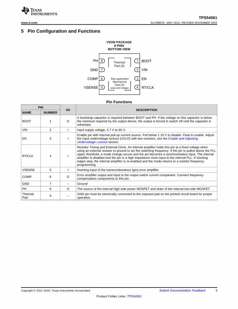
5 Pin Configuration and Functions
VSON PACKAGE8 PINS
BOTTOM VIEW
Pin FunctionsPIN
I/O DESCRIPTIONNAME NUMBER
A bootstrap capacitor is required between BOOT and PH. If the voltage on this capacitor is belowBOOT 1 O the minimum required by the output device, the output is forced to switch off until the capacitor is
refreshed.VIN 2 I Input supply voltage, 4.7 V to 60 V.
Enable pin with internal pull-up current source. Pull below 1.18 V to disable. Float to enable. AdjustEN 3 I the input undervoltage lockout (UVLO) with two resistors, see the Enable and Adjusting
Undervoltage Lockout section.Resistor Timing and External Clock. An internal amplifier holds this pin at a fixed voltage whenusing an external resistor to ground to set the switching frequency. If the pin is pulled above the PLLupper threshold, a mode change occurs and the pin becomes a synchronization input. The internalRT/CLK 4 I amplifier is disabled and the pin is a high impedance clock input to the internal PLL. If clockingedges stop, the internal amplifier is re-enabled and the mode returns to a resistor frequencyprogramming.
VSENSE 5 I Inverting input of the transconductance (gm) error amplifier.Error amplifier output and input to the output switch current comparator. Connect frequencyCOMP 6 O compensation components to this pin.
GND 7 – GroundPH 8 O The source of the internal high-side power MOSFET and drain of the internal low-side MOSFETThermal GND pin must be electrically connected to the exposed pad on the printed circuit board for proper9 –Pad operation.
Copyright © 2012–2015, Texas Instruments Incorporated Submit Documentation Feedback 3
Product Folder Links: TPS54061

TPS54061SLVSBB7E –MAY 2012–REVISED NOVEMBER 2015 www.ti.com
6 Specifications
6.1 Absolute Maximum Ratingsover operating free-air temperature (unless otherwise noted) (1)
MIN MAX UNITVIN –0.3 62 VEN (2) –0.3 8 VBOOT-PH –0.3 8 VVSENSE –0.3 6 V
VoltageCOMP –0.3 3 VPH –0.6 62 VPH, 10ns Transient –4 62 VRT/CLK –0.3 6 VVIN Internally Limited A
Current BOOT 100 mAPH Internally Limited A
Operating junction temperature –40 150 ºCStorage temperature, Tstg –65 150 °C
(1) Stresses beyond those listed under Absolute Maximum Ratings may cause permanent damage to the device. These are stress ratingsonly, which do not imply functional operation of the device at these or any other conditions beyond those indicated under RecommendedOperating Conditions. Exposure to absolute-maximum-rated conditions for extended periods may affect device reliability.
(2) See Enable and Adjusting UVLO section
6.2 ESD RatingsVALUE UNIT
Human body model (HBM), per ANSI/ESDA/JEDEC JS-001, all pins (1) ±2000V(ESD) Electrostatic discharge VCharged device model (CDM), per JEDEC specification JESD22-C101, ±500all pins (2)
(1) JEDEC document JEP155 states that 500-V HBM allows safe manufacturing with a standard ESD control process.(2) JEDEC document JEP157 states that 250-V CDM allows safe manufacturing with a standard ESD control process.
6.3 Recommended Operating Conditionsover operating free-air temperature range (unless otherwise noted)
MIN MAX UNITInput coltage 4.7 60 VOutput current 200 mASwitching frequency set by RT/CLK resistor 50 1100 kHzSwitching frequency synchronized to external clock 300 1100 kHz
6.4 Thermal InformationTPS54061
THERMAL METRIC (1) DRB UNIT8 PINS
RθJA Junction-to-ambient thermal resistance 42.9RθJC(top) Junction-to-case (top) thermal resistance 46.0RθJB Junction-to-board thermal resistance 18.1
°C/WψJT Junction-to-top characterization parameter 0.5ψJB Junction-to-board characterization parameter 18.3RθJC(bot) Junction-to-case (bottom) thermal resistance 3.0
(1) For more information about traditional and new thermal metrics, see the IC Package Thermal Metrics application report, SPRA953.
4 Submit Documentation Feedback Copyright © 2012–2015, Texas Instruments Incorporated
Product Folder Links: TPS54061

TPS54061www.ti.com SLVSBB7E –MAY 2012–REVISED NOVEMBER 2015
6.5 Electrical Characteristics (1)
TJ = –40°C to 150°C, VIN = 4.7 to 60 V (unless otherwise noted)PARAMETER TEST CONDITIONS MIN TYP MAX UNIT
SUPPLY VOLTAGE (VIN PIN)Operating input voltage VIN 4.7 60 VShutdown supply current EN = 0 V 1.4 µAIq Operating – Non switching VSENSE = 0.9 V, VIN = 12 V 90 110 µAENABLE AND UVLO (EN PIN)
Rising 1.23 1.4 VEnable threshold
Falling 1 1.18 VEnable threshold +50 mV –4.7 µA
Input currentEnable threshold –50 mV –1.2 µA
Hysteresis –3.5 µAEnable high to start switching time 450 µsVINVIN start voltage VIN rising 4.5 VVOLTAGE REFERENCE
TJ = 25°C, VIN = 12 V 0.792 0.8 0.808Voltage reference V
1mA < IOUT < Minimum Current Limit 0.784 0.8 0.816HIGH-SIDE MOSFETSwitch resistance BOOT-PH = 5.7 V 1.5 3.0 ΩLOW-SIDE MOSFETSwitch resistance VIN = 12 V 0.8 1.5 ΩERROR AMPLIFIERInput Current VSENSE pin 20 nAError amp gm –2µA < I(COMP) < 2µA, V(COMP) = 1 V 108 µSEA gm during slow start –2 µA < I(COMP) < 2 µA, V(COMP) = 1 V, VSENSE = 0.4 V 27 µSError amp DC gain VSENSE = 0.8V 1000 V/VMin unity gain bandwidth 0.5 MHzError amp source/sink V(COMP) = 1 V, 100 mV Overdrive ±8 µAStart-Switching Threshold 0.57 VCOMP to Iswitch gm 1.0 A/VCURRENT LIMITHigh-side sourcing current limit BOOT-PH = 5.7 V 250 350 500 mAthresholdZero cross detect current –1.1 mATHERMAL SHUTDOWNThermal shutdown 176 CRT/CLKOperating frequency using RT mode 50 1100 kHzSwitching frequency R(RT/CLK) = 120 kΩ 425 472 520 kHzMinimum CLK pulsewidth 40 nsRT/CLK voltage R(RT/CLK) = 120 kΩ 0.53 VRT/CLK high threshold 1.8 VRT/CLK low threshold 0.5 VRT/CLK falling edge to PH rising Measure at 500 kHz with RT resistor 60 nsedge delayPLL lock in time Measure at 500 kHz 100 µsPLL frequency range 300 1100 kHz
(1) The Electrical Characteristics specified in this section will apply to all specifications in this document unless otherwise noted.
Copyright © 2012–2015, Texas Instruments Incorporated Submit Documentation Feedback 5
Product Folder Links: TPS54061

TPS54061SLVSBB7E –MAY 2012–REVISED NOVEMBER 2015 www.ti.com
Electrical Characteristics(1) (continued)TJ = –40°C to 150°C, VIN = 4.7 to 60 V (unless otherwise noted)
PARAMETER TEST CONDITIONS MIN TYP MAX UNITPHMinimum On-time Measured at 50% to 50%, IOUT = 200 mA 120 nsDead time VIN = 12 V, IOUT = 200 mA, One transition 30 nsBOOTBOOT to PH regulation voltage VIN = 12 V 6.0 VBOOT-PH UVLO 2.9 VINTERNAL SLOW-START TIMESlow-Start time fSW = 472 kHz, RT = 120 kΩ, 10% to 90% 2.36 ms
6 Submit Documentation Feedback Copyright © 2012–2015, Texas Instruments Incorporated
Product Folder Links: TPS54061
400
420
440
460
480
500
520
540
-50 -25 0 25 50 75 100 125 150
T - Junction Temperature - °CJ
V = 12 V,
R = 120 k
IN
T W
f-
Os
cil
lato
r F
req
ue
nc
y -
kH
zsw
0
100
200
300
400
500
600
700
800
900
1000
1100
25 100 1000 2500Timing Resistance (kΩ)
Osc
illat
or F
requ
ency
(kH
z)
VIN = 12 VTJ = 25°C
G001
0
20
40
60
80
100
120
% o
f N
orm
al -
f sw
Falling
0 100 200 300 400 500 600 700 800
V - Feedback Voltage - mVSENSE
Rising
V = 12 V,
R = 120 k
T = 25°C
IN
T W
J
0.787
0.789
0.791
0.793
0.795
0.797
0.799
0.801
0.803
–50 –25 0 25 50 75 100 125 150
V–
Vo
lta
ge
Re
fere
nc
e–
VR
EF
T – Junction Temperature – DegJ
-50 -25 0 25 50 75 100 125 150
T - Junction Temperature - °CJ
0
0.5
1
1.5
2
2.5
3
R-
On
Resis
tan
ce -
ds
on
W
VIN = 12 V
-50 -25 0 25 50 75 100 125 150
T - Junction Temperature - °CJ
0
0.2
0.4
0.6
0.8
1
1.2
1.4
R-
On
Resis
tan
ce -
dso
nW
VIN = 12 V
TPS54061www.ti.com SLVSBB7E –MAY 2012–REVISED NOVEMBER 2015
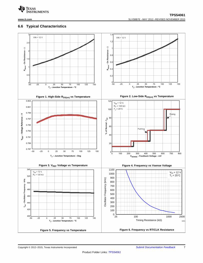
6.6 Typical Characteristics
Figure 2. Low-Side RDS(on) vs TemperatureFigure 1. High-Side RDS(on) vs Temperature
Figure 3. VREF Voltage vs Temperature Figure 4. Frequency vs Vsense Voltage
Figure 6. Frequency vs RT/CLK ResistanceFigure 5. Frequency vs Temperature
Copyright © 2012–2015, Texas Instruments Incorporated Submit Documentation Feedback 7
Product Folder Links: TPS54061
0
0.5
1
1.5
2
2.5
3
0 5 10 15 20 25 30 35 40 45 50 55 60
V Input Voltage (V)I -
IS
hu
tdo
wn
Cu
rre
nt
(A
)sd-
µ
TJ = 150°C
TJ = −40°C
TJ = 25°C
EN = 0 V
G002
-1.5
-1.45
-1.4
-1.35
-1.3
-1.25
-1.2
-1.15
-1.1
-1.05
-1
0 5 10 15 20 25 30 35 40 45 50 55 60
En
ab
le C
urr
en
t -
Am
V - Input Voltage - VI
V = 12 V
T =
IN
J25°C
-3.75
-3.70
-3.65
-3.60
-3.55
-3.50
-3.45
-3.40
-3.35
-50 -25 0 25 50 75 100 125 150
T - Junction Temperature - °CJ
V = 12 VIN
En
ab
le H
ys
tere
sis
Cu
rre
nt
-A
μ
4
4.05
4.1
4.15
4.2
4.25
4.3
4.35
4.4
4.45
4.5
4.55
4.6
-50 -25 0 25 50 75 100 125 150
T - Junction Temperature - °CJ
V-
Inp
ut
Vo
lta
ge
- V
I
UVLO Start
UVLO Stop
-50 -25 0 25 50 75 100 125 150
T - Junction Temperature - °CJ
V = 12 VIN V RisingEN
V FallingEN
1.10
1.12
1.14
1.16
1.18
1.20
1.22
1.24
1.26
VE
NA
- E
na
ble
Vo
lta
ge
- V
0
20
40
60
80
100
120
140
-50 -25 0 25 50 75 100 125 150
T - Junction Temperature - °CJ
Tra
nsco
nd
ucta
nce -
mS
V = 12 VIN
TPS54061SLVSBB7E –MAY 2012–REVISED NOVEMBER 2015 www.ti.com
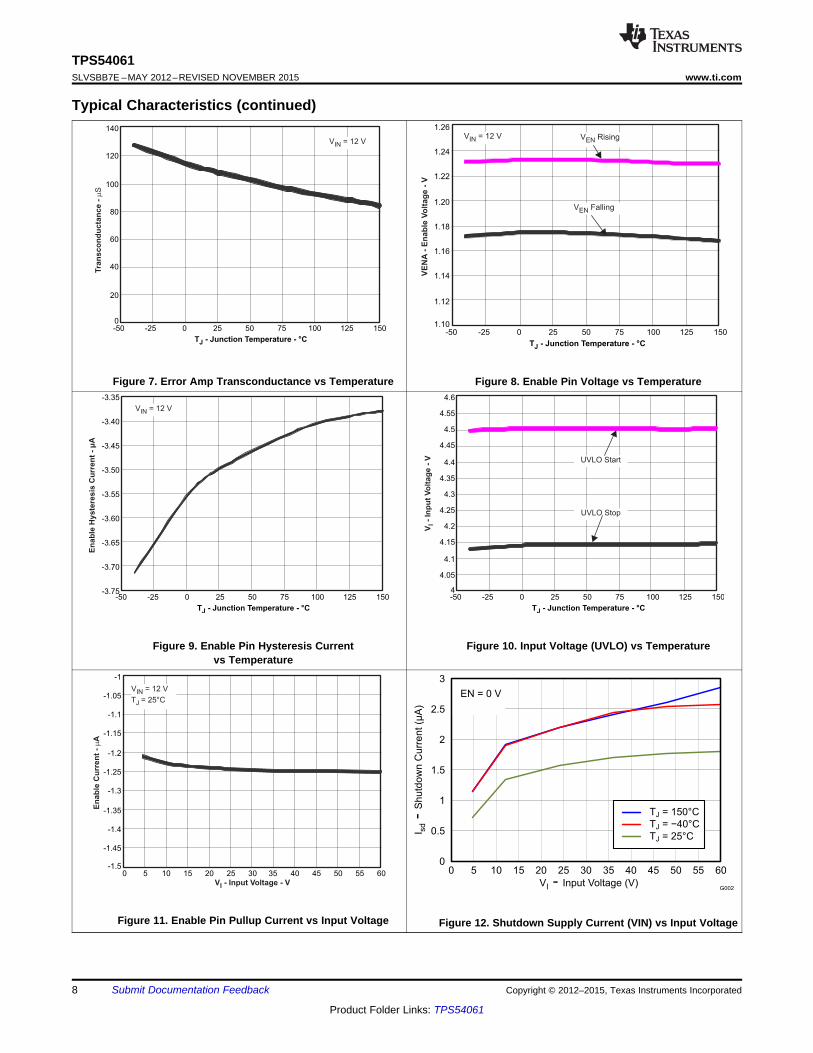
Typical Characteristics (continued)
Figure 7. Error Amp Transconductance vs Temperature Figure 8. Enable Pin Voltage vs Temperature
Figure 9. Enable Pin Hysteresis Current Figure 10. Input Voltage (UVLO) vs Temperaturevs Temperature
Figure 11. Enable Pin Pullup Current vs Input Voltage Figure 12. Shutdown Supply Current (VIN) vs Input Voltage
8 Submit Documentation Feedback Copyright © 2012–2015, Texas Instruments Incorporated
Product Folder Links: TPS54061

0.2
0.25
0.3
0.35
0.4
0.45
T = 25°CJ
T = -40°CJ
T = 150°CJ
Cu
rren
t L
imit
Th
resh
old
-A
5 10 15 20 25 30 35 40 45 50 55 60
V - Input Voltage - VI
0
-50 -25 0 25 50 75 100 125 150
T - Junction Temperature - °CJ
2.32
2.34
2.36
2.38
2.40
2.42
2.44
2.46
2.48
t-
SS
Tim
e -
ms
SS
V = 12 V,
f = 472 kHzIN
sw
0 1 2 3 4 5
V - Input Voltage - VI
0
20
40
60
80
100
120
140
160
Su
pp
ly C
urr
en
t -
Am
T = 25°CJ
T = -40°CJ
T = 150°CJ
EN = Open
80
82
84
86
88
90
92
94
96
98
0 5 10 15 20 25 30 35 40 45 50 55 60Input Voltage (V)
Sup
ply
Cur
rent
(µA
)
TJ = 150°CTJ = −40°CTJ = 25°C
EN = OpenVSENSE = 0.83 V
G003
0
0.25
0.5
0.75
1
1.25
1.5
1.75
2
0 1 2 3 4 5Input Voltage (V)
Sup
ply
Cur
rent
(µA
)
TJ = 150°CTJ = −40°CTJ = 25°C
EN = 0 V
G004
TPS54061www.ti.com SLVSBB7E –MAY 2012–REVISED NOVEMBER 2015
Typical Characteristics (continued)
Figure 13. Supply Current (VIN Pin) vs Input Voltage Figure 14. Supply Current (VIN Pin)vs Input Voltage (0 V to VSTART) En Pin Low
Figure 15. Supply Current (VIN Pin) vs Figure 16. Slow-Start Time vs TemperatureInput Voltage (0 V to VSTART) En Pin Open
Figure 17. Current Limit vs Input Voltage
Copyright © 2012–2015, Texas Instruments Incorporated Submit Documentation Feedback 9
Product Folder Links: TPS54061
TPS54061SLVSBB7E –MAY 2012–REVISED NOVEMBER 2015 www.ti.com
7 Detailed Description
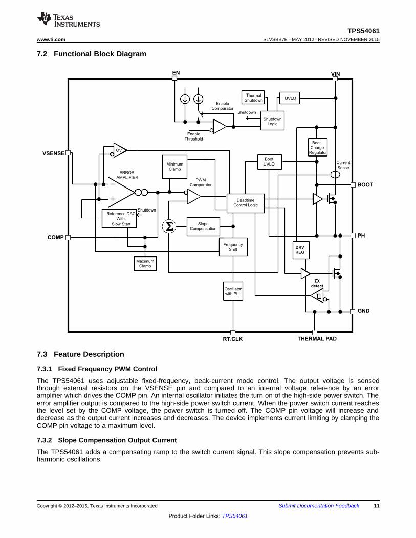
7.1 OverviewThe TPS54061 device is a 60-V, 200-mA, step-down (buck) regulator with an integrated high-side and low-siden-channel MOSFET. To improve performance during line and load transients the device implements a constantfrequency, current mode control which reduces output capacitance and simplifies external frequencycompensation design.
The switching frequency of 50 kHz to 1100 kHz allows for efficiency and size optimization when selecting theoutput filter components. The switching frequency is adjusted using a resistor-to-ground on the RT/CLK pin. Thedevice has an internal phase-lock loop (PLL) on the RT/CLK pin that is used to synchronize the power switchturn on to a falling edge of an external system clock.
The TPS54061 has a default startup voltage of approximately 4.5 V. The EN pin has an internal pullup currentsource that can be used to adjust the input voltage UVLO threshold with two external resistors. In addition, thepullup current provides a default condition. When the EN pin is floating the device will operate. The operatingcurrent is 90 µA when not switching and under no load. When the device is disabled, the supply current is 1.4µA.
The integrated 1.5-Ω high-side MOSFET and 0.8-Ω low-side MOSFET allows for high-efficiency power supplydesigns capable of delivering 200 milliamperes of continuous current to a load.
The TPS54061 reduces the external component count by integrating the boot recharge diode. The bias voltagefor the integrated high-side MOSFET is supplied by a capacitor on the BOOT to PH pin. The boot capacitorvoltage is monitored by an UVLO circuit and will turn the high-side MOSFET off when the boot voltage fallsbelow a preset threshold. The TPS54061 can operate at high duty cycles because of the boot UVLO. The outputvoltage can be adjusted down to as low as the 0.8-V reference.
The TPS54061 has an internal output OV protection that disables the high-side MOSFET if the output voltage is109% of the nominal output voltage.
The TPS54061 reduces external component count by integrating the slow-start time using a reference DACsystem.
The TPS54061 resets the slow-start times during overload conditions with an overload recovery circuit. Theoverload recovery circuit will slow start the output from the fault voltage to the nominal regulation voltage once afault condition is removed. A frequency foldback circuit reduces the switching frequency during startup andovercurrent fault conditions to help control the inductor current.
10 Submit Documentation Feedback Copyright © 2012–2015, Texas Instruments Incorporated
Product Folder Links: TPS54061
ERROR
AMPLIFIER
Boot
Regulator
Boot
UVLO
UVLO
Current
Sense
Oscillator
with PLL
Frequency
Shift
Deadtime
Control Logic
Slope
Compensation
PWM
Comparator
Minimum
Clamp
Maximum
Clamp
Slow Start
With
VSENSE
COMP
THERMAL PAD
PH
BOOT
VIN
GND
Thermal
Shutdown
EN
Enable
Comparator
Shutdown
Logic
Shutdown
Enable
Threshold
Shutdown
OV
DRV
REG
ZX
detect
RT/CLK
Charge
Reference DAC
TPS54061www.ti.com SLVSBB7E –MAY 2012–REVISED NOVEMBER 2015
7.2 Functional Block Diagram
7.3 Feature Description
7.3.1 Fixed Frequency PWM ControlThe TPS54061 uses adjustable fixed-frequency, peak-current mode control. The output voltage is sensedthrough external resistors on the VSENSE pin and compared to an internal voltage reference by an erroramplifier which drives the COMP pin. An internal oscillator initiates the turn on of the high-side power switch. Theerror amplifier output is compared to the high-side power switch current. When the power switch current reachesthe level set by the COMP voltage, the power switch is turned off. The COMP pin voltage will increase anddecrease as the output current increases and decreases. The device implements current limiting by clamping theCOMP pin voltage to a maximum level.
7.3.2 Slope Compensation Output CurrentThe TPS54061 adds a compensating ramp to the switch current signal. This slope compensation prevents sub-harmonic oscillations.
Copyright © 2012–2015, Texas Instruments Incorporated Submit Documentation Feedback 11
Product Folder Links: TPS54061

ENAFALLING
START STOP
ENARISING
UVLO
ENAFALLING
HYS
ENARISING
VV V
VR 1 =
VI1 × 1 + I
V
æ ö-ç ÷
è ø
æ ö-ç ÷
è ø
TPS54061
i
VIN
Ruvlo1
Ruvlo2
EN
OptionalVEN
ihys1
V 0.8 VOUT
R = RHS LS 0.8 V
-æ ö´ ç ÷ç ÷
è ø
TPS54061SLVSBB7E –MAY 2012–REVISED NOVEMBER 2015 www.ti.com
Feature Description (continued)7.3.3 Error AmplifierThe TPS54061 uses a transconductance amplifier for the error amplifier. The error amplifier compares theVSENSE voltage to the lower of the internal slow-start voltage or the internal 0.8-V voltage reference. Thetransconductance (gm) of the error amplifier is 108 µA/V during normal operation. During the slow-startoperation, the transconductance is a fraction of the normal operating gm. The frequency compensationcomponents (capacitor, series resistor and capacitor) are added to the COMP pin-to-ground.
7.3.4 Voltage ReferenceThe voltage reference system produces a precise voltage reference over temperature by scaling the output of atemperature stable band-gap circuit
7.3.5 Adjusting the Output VoltageThe output voltage is set with a resistor divider from the output node to the VSENSE pin. TI recommends using1% tolerance or better divider resistors. Start with a 10-kΩ for the RLS resistor and use the Equation 1 tocalculate RHS.
(1)
7.3.6 Enable and Adjusting UVLOThe TPS54061 is enabled when the VIN pin voltage rises above 4.5 V and the EN pin voltage exceeds the ENrising threshold of 1.23 V. The EN pin has an internal pullup current source, I1, of 1.2 µA that provides thedefault enabled condition when the EN pin floats.
If an application requires a higher input UVLO threshold, use the circuit shown in Figure 18 to adjust the inputvoltage UVLO with two external resistors. When the EN pin voltage exceeds 1.23 V, an additional 3.5 µA ofhysteresis current, Ihys, is sourced out of the EN pin. When the EN pin is pulled below 1.18 V, the 3.5-µA Ihyscurrent is removed. This additional current facilitates adjustable input voltage hysteresis. Use Equation 2 tocalculate RUVLO1 for the desired input start and stop voltages . Use Equation 3 to similarly calculate RUVLO2.
In applications designed to start at relatively low input voltages (for example, from 4.7 V to 10 V) and withstandhigh input voltages (for example, from 40 V to 60 V), the EN pin may experience a voltage greater than theabsolute maximum voltage of 8 V during the high input voltage condition. TI recommends using a zener diode toclamp the pin voltage below the absolute maximum rating.
Figure 18. Adjustable Undervoltage Lock-Out
(2)
12 Submit Documentation Feedback Copyright © 2012–2015, Texas Instruments Incorporated
Product Folder Links: TPS54061

OUTSC LS CL DC CLSW
ON IN CL HS CL LS
V + R × I + R Idiv(shift) = ×
t V I R + I R
ff
æ ö æ ö´ç ÷ ç ÷
- ´ ´è ø è ø
OUT LS O DC OSW
ON IN O HS O LS
V + R I + R I1(maxskip) =
t V I R + I Rf
æ ö æ ö´ ´´ç ÷ ç ÷
- ´ ´è ø è ø
T
SW1.039
71657R (k ) =
(kHz)W
f
SW
1114tss(ms) =
(kHz)f
( )UVLO ENAFALLING
UVLO
STOP ENAFALLING UVLO 1 HYS
R 1 VR 2 =
V V + R 1 I + I
´
- ´
TPS54061www.ti.com SLVSBB7E –MAY 2012–REVISED NOVEMBER 2015
Feature Description (continued)
(3)
7.3.7 Internal Slow-StartThe TPS54061 has an internal digital slow-start that ramps the reference voltage from zero volts to its final valuein 1114 switching cycles. The internal slow-start time is calculated by the following expression:
(4)
If the EN pin is pulled below the stop threshold of 1.18 V, switching stops and the internal slow-start resets. Theslow-start also resets in thermal shutdown.
7.3.8 Constant Switching Frequency and Timing Resistor (RT/CLK Pin)The switching frequency of the TPS54061 is adjustable over a wide range from 50 kHz to 1100 kHz by varyingthe resistor on the RT/CLK pin. The RT/CLK pin voltage is typically 0.53 V and must have a resistor-to-ground toset the switching frequency. To determine the timing resistance for a given switching frequency, use Equation 5.To reduce the solution size, one would typically set the switching frequency as high as possible, but tradeoffs ofthe supply efficiency, maximum input voltage and minimum controllable on-time should be considered. Theminimum controllable on-time is typically 120 ns and limits the operating frequency for high input voltages. Themaximum switching frequency is also limited by the frequency shift circuit. More discussion on the details of themaximum switching frequency is located below.
(5)
7.3.9 Selecting the Switching FrequencyThe TPS54061 implements current-mode control which uses the COMP pin voltage to turn off the high-sideMOSFET on a cycle-by-cycle basis. Each cycle the switch current and COMP pin voltage are compared, whenthe peak switch current intersects the COMP voltage, the high-side switch is turned off. During overcurrentconditions that pull the output voltage low, the error amplifier will respond by driving the COMP pin high,increasing the switch current. The error amplifier output is clamped internally, which functions as a switch currentlimit.
To enable higher switching frequency at high input voltages, the TPS54061 implements a frequency shift. Theswitching frequency is divided by 8, 4, 2, and 1 as the voltage ramps from 0 to 0.8 volts on VSENSE pin. Thedevice implements a digital frequency shift to enable synchronizing to an external clock during normal startupand fault conditions. Because the device can only divide the switching frequency by 8, there is a maximum inputvoltage limit in which the device operates and still have frequency shift protection. During short-circuit events(particularly with high input voltage applications), the control loop has a finite minimum controllable on-time andthe output has a low voltage. During the switch-on time, the inductor current ramps to the peak current limitbecause of the high input voltage and minimum on-time. During the switch-off time, the inductor would normallynot have enough off-time and output voltage for the inductor to ramp down by the ramp up amount. Thefrequency shift effectively increases the off-time allowing the current to ramp down.
(6)
Where• IO = Output current• ICL = Current Limit• VIN = Input Voltage• VOUT = Output Voltage
Copyright © 2012–2015, Texas Instruments Incorporated Submit Documentation Feedback 13
Product Folder Links: TPS54061

RT/CLK
TPS54061
Clock
Source
PLL
RT
RT/CLK
TPS54061
Hi-Z
Clock
Source
PLL
RT
TPS54061SLVSBB7E –MAY 2012–REVISED NOVEMBER 2015 www.ti.com
Feature Description (continued)• VOUTSC Output Voltage during short• RDC = Inductor resistance• RHS = High-side MOSFET resistance• RLS = Low-side MOSFET resistance• ton = Controllable on-time• fdiv = Frequency divide (equals 1, 2, 4, or 8) (7)
7.3.10 Synchronization to RT/CLK PinThe RT/CLK pin can be used to synchronize the regulator to an external system clock. To implement thesynchronization feature connect a square wave to the RT/CLK pin through one of the circuit networks shown inFigure 19. The square-wave amplitude must extend lower than 0.5 V and higher than 1.8 V on the RT/CLK pinand have high and low states greater than 40 ns. The synchronization frequency range is 300 kHz to 1100 kHz.The rising edge of the PH will be synchronized to the falling edge of RT/CLK pin signal. The externalsynchronization circuit should be designed in such a way that the device will have the default frequency setresistor connected from the RT/CLK pin-to-ground should the synchronization signal turn off. TI recommendsusing a frequency set resistor connected as shown in Figure 19 through another resistor-to-ground (e.g., 50 Ω)for clock signal that are not Hi-Z or tristate during the off state. The sum of the resistance should set theswitching frequency close to the external CLK frequency. TI recommends to AC couple the synchronizationsignal through a 10-pF ceramic capacitor to RT/CLK pin. The first time the CLK is pulled above the CLKthreshold the device switches from the RT resistor frequency to PLL mode. The internal 0.5 V voltage source isremoved and the CLK pin becomes high impedance as the PLL starts to lock onto the external signal. Theswitching frequency can be higher or lower than the frequency set with the RT/CLK resistor. The devicetransitions from the resistor mode to the PLL mode and lock onto the CLK frequency within 100 microseconds.When the device transitions from the PLL mode to the resistor mode, the switching frequency will reduce fromthe external CLK frequency to 150 kHz, then reapply the 0.5-V voltage source and the resistor will then set theswitching frequency. The switching frequency is divided by 8, 4, 2, and 1 as the voltage ramps from 0 to 0.8 voltson VSENSE pin. The device implements a digital frequency shift to enable synchronizing to an external clockduring normal startup and fault conditions.
Figure 19. Synchronizing to a System Clock
7.3.11 Overvoltage ProtectionThe TPS54061 incorporates an output overvoltage transient protection (OVP) circuit to minimize voltageovershoot when recovering from output fault conditions or strong unload transients on power supply designs withlow-value output capacitance. For example, when the power supply output is overloaded the error amplifiercompares the actual output voltage to the internal reference voltage. If the VSENSE pin voltage is lower than theinternal reference voltage for a considerable time, the output of the error amplifier will respond by clamping theerror amplifier output to a high voltage. Thus, requesting the maximum output current. Once the condition isremoved, the regulator output rises and the error amplifier output transitions to the steady-state duty cycle. Insome applications, the power supply output voltage can respond faster than the error amplifier output canrespond, this actuality leads to the possibility of an output overshoot.
The OVP feature minimizes the output overshoot when using a low-value output capacitor by comparing theVSENSE pin voltage to OVP threshold which is 109% of the internal voltage reference. If the VSENSE pinvoltage is greater than the OVP threshold, the high-side MOSFET is disabled to minimize output overshoot.When the VSENSE voltage drops lower than the OVP threshold, the high-side MOSFET resumes normaloperation.
14 Submit Documentation Feedback Copyright © 2012–2015, Texas Instruments Incorporated
Product Folder Links: TPS54061

TPS54061www.ti.com SLVSBB7E –MAY 2012–REVISED NOVEMBER 2015
Feature Description (continued)7.3.12 Thermal ShutdownThe device implements an internal thermal shutdown until the junction temperature exceeds 176°C. The thermalshutdown forces the device to stop switching until the junction temperature falls below the thermal trip threshold.Once the die temperature decreases below 176°C, the device reinitiates the power-up sequence by restarting theinternal slow-start.
7.4 Device Functional Modes
7.4.1 Operation Near Minimimum Input VoltageThe TPS54061 is recommended to operate with input voltages above 4.7 V. The typical VIN UVLO threshold is4.5 V and the device may operate at input voltages down to the UVLO voltage. At input voltages below the actualUVLO voltage the device will not switch. If EN is floating or externally pulled up to greater up than the typical1.23 V rising threshold, when V(VIN) passes the UVLO threshold the TPS54061 will become active. Switching isenabled and the slow-start sequence is initiated. The TPS54061 starts linearly ramping up the internal referenceDAC from 0 V to the reference voltage over the internal slow-start time period set by the switching frequency.
7.4.2 Operation With Enable ControlThe enable start threshold voltage is 1.23 V typical. With EN held below the 1.23 V typical rising thresholdvoltage the TPS54061 is disabled and switching is inhibited even if VIN is above its UVLO threshold. Thequiescent current is reduced in this state. If the EN voltage is increased above the rising threshold voltage whileV(VIN) is above the UVLO threshold, the device becomes active. Switching is enabled and the slow-startsequence is initiated. The TPS54061 starts linearly ramping up the internal reference DAC from 0 V to thereference voltage over the internal slow-start time period set by the switching frequency. If EN is pulled below the1.18 V typical falling threshold the TPS54061 will enter the reduced quiescent current state again.
Copyright © 2012–2015, Texas Instruments Incorporated Submit Documentation Feedback 15
Product Folder Links: TPS54061

CIN
LO
8 V to 60 V
0.01 Fμ
100 HμU1
TPS54061 3.3 V 200 mA1 2
RT
31.6 kΩ
CPOLE
36.5 kΩ
RHS
2.2 Fμ
CBOOT
RUVLO233 pF
CCOMP
4700 pF
10 kΩ
RLS
26.1 kΩ
RCOMP
RUVLO1
143 kΩ
196 kΩ
CO
10 Fμ
2
3 6
1
4
7
8
5
*
TPS54061SLVSBB7E –MAY 2012–REVISED NOVEMBER 2015 www.ti.com
8 Application and Implementation
NOTEInformation in the following applications sections is not part of the TI componentspecification, and TI does not warrant its accuracy or completeness. TI’s customers areresponsible for determining suitability of components for their purposes. Customers shouldvalidate and test their design implementation to confirm system functionality.
8.1 Application InformationThe TPS54061 is a 60-V, 200-mA step-down regulator with an integrated high-side and low-side MOSFET. Thisdevice is typically used to convert a higher DC voltage to a lower DC voltage with a maximum available outputcurrent of 200 mA. Example applications are: Low-Power Standby or Bias Voltage Supplies, 4-20 mA CurrentLoop Powered Sensors, Industrial Process Control, Metering, and Security Systems or an efficient high voltagelinear regulator replacement. Use the following design procedure to select component values for the TPS54061.This procedure illustrates the design of a high-frequency switching regulator. These calculations can be donewith the aid of the excel spreadsheet tool SLVC431. Alternatively, use the WEBENCH software to generate acomplete design. The WEBENCH software uses an iterative design procedure and accesses a comprehensivedatabase of components when generating a design.
8.2 Typical Applications
8.2.1 CCM Application
* See Enable and Adjusting Undervoltage Lockout section
Figure 20. CCM Application Schematic
8.2.1.1 Design RequirementsThis example details the design of a continuous conduction mode (CCM) switching regulator design usingceramic output capacitors. If a low-output current design is needed, see DCM Application. A few parametersmust be known in order to start the design process. These parameters are typically determined at the systemlevel. For this example, we will start with the following known parameters:
Table 1. Design ParametersPARAMETERS VALUES
Output Voltage 5.0 VTransient Response 50 to 150mA load step ΔVOUT = 4%Maximum Output Current 200 mAInput Voltage 24 V nom. 8 V to 60 VOutput Voltage Ripple 0.5% of VOUT
16 Submit Documentation Feedback Copyright © 2012–2015, Texas Instruments Incorporated
Product Folder Links: TPS54061
( )OUT IN OUT
RIPPLE
IN O SW
V V max VI
V max L f
´ -³
´ ´
IN OUT OUT
IN sw
V max V VL min
O Kind I V maxO
-³ ´
´ ´ ¦
TPS54061www.ti.com SLVSBB7E –MAY 2012–REVISED NOVEMBER 2015
Typical Applications (continued)Table 1. Design Parameters (continued)
PARAMETERS VALUESStart Input Voltage (rising VIN) 7.50 VStop Input Voltage (falling VIN) 6.50 V
8.2.1.2 Detailed Design Procedure
8.2.1.2.1 Selecting the Switching Frequency
The first step is to decide on a switching frequency for the regulator. Typically, the user will want to choose thehighest switching frequency possible because this will produce the smallest solution size. The high switchingfrequency allows for lower valued inductors and smaller output capacitors compared to a power supply thatswitches at a lower frequency. The switching frequency is limited by the minimum on-time of the internal powerswitch, the maximum input voltage, the output voltage and the frequency shift limitation.
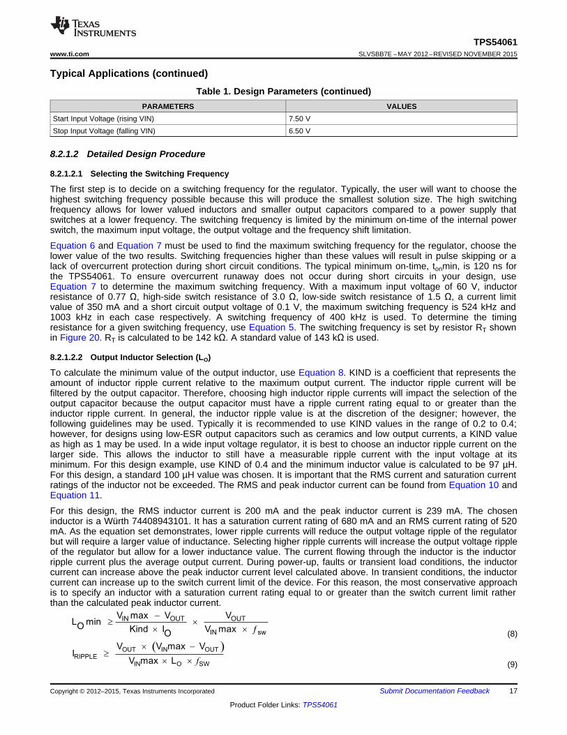
Equation 6 and Equation 7 must be used to find the maximum switching frequency for the regulator, choose thelower value of the two results. Switching frequencies higher than these values will result in pulse skipping or alack of overcurrent protection during short circuit conditions. The typical minimum on-time, tonmin, is 120 ns forthe TPS54061. To ensure overcurrent runaway does not occur during short circuits in your design, useEquation 7 to determine the maximum switching frequency. With a maximum input voltage of 60 V, inductorresistance of 0.77 Ω, high-side switch resistance of 3.0 Ω, low-side switch resistance of 1.5 Ω, a current limitvalue of 350 mA and a short circuit output voltage of 0.1 V, the maximum switching frequency is 524 kHz and1003 kHz in each case respectively. A switching frequency of 400 kHz is used. To determine the timingresistance for a given switching frequency, use Equation 5. The switching frequency is set by resistor RT shownin Figure 20. RT is calculated to be 142 kΩ. A standard value of 143 kΩ is used.
8.2.1.2.2 Output Inductor Selection (LO)
To calculate the minimum value of the output inductor, use Equation 8. KIND is a coefficient that represents theamount of inductor ripple current relative to the maximum output current. The inductor ripple current will befiltered by the output capacitor. Therefore, choosing high inductor ripple currents will impact the selection of theoutput capacitor because the output capacitor must have a ripple current rating equal to or greater than theinductor ripple current. In general, the inductor ripple value is at the discretion of the designer; however, thefollowing guidelines may be used. Typically it is recommended to use KIND values in the range of 0.2 to 0.4;however, for designs using low-ESR output capacitors such as ceramics and low output currents, a KIND valueas high as 1 may be used. In a wide input voltage regulator, it is best to choose an inductor ripple current on thelarger side. This allows the inductor to still have a measurable ripple current with the input voltage at itsminimum. For this design example, use KIND of 0.4 and the minimum inductor value is calculated to be 97 µH.For this design, a standard 100 µH value was chosen. It is important that the RMS current and saturation currentratings of the inductor not be exceeded. The RMS and peak inductor current can be found from Equation 10 andEquation 11.
For this design, the RMS inductor current is 200 mA and the peak inductor current is 239 mA. The choseninductor is a Würth 74408943101. It has a saturation current rating of 680 mA and an RMS current rating of 520mA. As the equation set demonstrates, lower ripple currents will reduce the output voltage ripple of the regulatorbut will require a larger value of inductance. Selecting higher ripple currents will increase the output voltage rippleof the regulator but allow for a lower inductance value. The current flowing through the inductor is the inductorripple current plus the average output current. During power-up, faults or transient load conditions, the inductorcurrent can increase above the peak inductor current level calculated above. In transient conditions, the inductorcurrent can increase up to the switch current limit of the device. For this reason, the most conservative approachis to specify an inductor with a saturation current rating equal to or greater than the switch current limit ratherthan the calculated peak inductor current.
(8)
(9)
Copyright © 2012–2015, Texas Instruments Incorporated Submit Documentation Feedback 17
Product Folder Links: TPS54061
RIPPLEL OUT
II peak = I +
2
( )2
OUT IN OUT2
L O
IN O SW
V V max V1I rms = I +
12 V max L f
æ ö´ -´ ç ÷ç ÷´ ´è ø
TPS54061SLVSBB7E –MAY 2012–REVISED NOVEMBER 2015 www.ti.com
(10)
(11)
8.2.1.2.3 Output Capacitor
There are three primary considerations for selecting the value of the output capacitor. The output capacitor willdetermine the modulator pole, the output voltage ripple, and how the regulator responds to a large change inload current. The output capacitance needs to be selected based on the most stringent of these three criteria.The desired response to a large change in the load current is the first criteria. The output capacitor needs tosupply the load with current until the regulator increases the inductor current. This situation would occur if thereare desired hold-up times for the regulator where the output capacitor must hold the output voltage above acertain level for a specified amount of time after the input power is removed. The regulator also will temporarilynot be able to supply sufficient output current if there is a large, fast increase in the current needs of the loadsuch as transitioning from no load to a full load. The regulator usually needs two or more clock cycles for thecontrol loop to see the change in load current and output voltage and adjust the duty cycle to react to thechange. The output capacitor must be sized to supply the extra current to the load until the control loop respondsto the load change. The output capacitance must be large enough to supply the difference in current for 2 clockcycles while only allowing a tolerable amount of droop in the output voltage. Equation 15 shows the minimumoutput capacitance necessary to accomplish this, where ΔIout is the change in output current, ƒsw is theregulators switching frequency and ΔVout is the allowable change in the output voltage.
For this example, the transient load response is specified as a 4% change in Vout for a load step from 50 mA to150 mA. For this example, ΔIOUT = 0.150 –0.05 = 0.10 and ΔVOUT = 0.04 × 3.3 = 0.132.
Using these values gives a minimum capacitance of 3.79 µF. This does not take the ESR of the output capacitorinto account in the output voltage change. For ceramic capacitors, the ESR is usually small enough to ignore inthis calculation. Aluminum electrolytic and tantalum capacitors have higher ESR that should be taken intoaccount.
The low side FET of the regulator emulates a diode so it can not sink current so any stored energy in theinductor will produce an output voltage overshoot when the load current rapidly decreases, as in Figure 28. Theoutput capacitor must also be sized to absorb energy stored in the inductor when transitioning from a high loadcurrent to a lower load current. The excess energy that gets stored in the output capacitor will increase thevoltage on the capacitor. The capacitor must be sized to maintain the desired output voltage during thesetransient periods. Equation 14 is used to calculate the minimum capacitance input the output voltage overshootto a desired value, where LO is the value of the inductor, IOH is the output current under heavy load, IOL is theoutput under light load, VO+ΔVO is the final peak output voltage, and Vi is the initial capacitor voltage. For thisexample, the worst case load step will be from 150 mA to 50 mA. The output voltage will increase during thisload transition and must be limited to 4% of the output voltage to satisy the design goal. This will make VO+ΔVO= 1.04 × 3.3 = 3.432 V. VO is the initial capacitor voltage which is the nominal output voltage of 3.3 V. Usingthese numbers in Equation 14 yields a minimum capacitance of 2.25 µF.
Equation 13 calculates the minimum output capacitance needed to meet the output voltage ripple specification,where fSW is the switching frequency, Vripple is the maximum allowable output voltage ripple, and Iripple is theinductor ripple current. Equation 13 yields 1.48 µF. Equation 16 calculates the maximum ESR an outputcapacitor can have to meet the output voltage ripple specification. Equation 16 indicates the ESR should be lessthan 0.160 Ω.
The most stringent criteria for the output capacitor is 3.79 µF of capacitance to maintain the output voltageregulation during an load transient.
Additional capacitance de-ratings for aging, temperature and DC bias will increase this minimum value. For thisexample, a 10-µF, 10-V X5R ceramic capacitor with 0.003 Ω of ESR in a 1206 package is used.
Capacitors generally have limits to the amount of ripple current they can handle without failing or producingexcess heat. An output capacitor that can support the inductor ripple current must be specified. Some capacitordata sheets specify the Root Mean Square (RMS) value of the maximum ripple current.
Equation 12 can be used to calculate the RMS ripple current the output capacitor needs to support. For thisexample, Equation 12 yields 10.23 mA.18 Submit Documentation Feedback Copyright © 2012–2015, Texas Instruments Incorporated
Product Folder Links: TPS54061
OIN
IN SW
I 0.25C
V ripple f
æ ö³ ´ ç ÷
è ø
( )INmin OUTOUTIN OUT
INmin INmin
V VVIC rms I
V V
-= ´ ´
RIPPLE
C
RIPPLE
VR
I£
OUT
O
OUT
I 2C 3
V sw
D³ ´
D f
( )
2 2
OH OL
O O 2 2
OUT OUT OUT
I IC 2 L
V + V V
-³ ´
D -
RIPPLE
O
RIPPLE SW
I 1C 1
V 8 f
æ ö³ ´ ç ÷
´è ø
( )OUT IN OUT
O
IN O SW
V V max V1IC rms =
V max L12 f
æ ö´ -´ ç ÷ç ÷´ ´è ø
TPS54061www.ti.com SLVSBB7E –MAY 2012–REVISED NOVEMBER 2015
(12)
(13)
(14)
(15)
(16)
8.2.1.2.4 Input Capacitor
The TPS54061 requires a high-quality ceramic, type X5R or X7R, input decoupling capacitor of at least 1 µF ofeffective capacitance. The effective capacitance includes any deration for DC bias effects. The voltage rating ofthe input capacitor must be greater than the maximum input voltage. The capacitor must also have an RMScurrent rating greater than the maximum RMS input current. The input RMS current can be calculated usingEquation 17. The value of a ceramic capacitor varies significantly over temperature and the dc bias applied to thecapacitor. The capacitance variations with temperature can be minimized by selecting a dielectric material that isstable over temperature. X5R and X7R ceramic dielectrics are usually selected for power regulator capacitorsbecause they have a high capacitance to volume ratio and are fairly stable over temperature. The effective valueof a capacitor decreases as the DC bias across a capacitor increases. For this example design, a ceramiccapacitor with at least a 60-V voltage rating is required to support the maximum input voltage. The inputcapacitance value determines the input ripple voltage of the regulator. The input voltage ripple can be calculatedby rearranging Equation 18.
Using the design example values, Ioutmax = 200 mA, CIN = 2.2 µF, ƒSW = 400 kHz, yields an input voltage rippleof 56.8 mV and an RMS input ripple current of 98.5 mA.
(17)
(18)
8.2.1.2.5 Bootstrap Capacitor Selection
A 0.01-µF ceramic capacitor must be connected between the BOOT and PH pins for proper operation. TIrecommends using a ceramic capacitor with X5R or better grade dielectric. The capacitor should have 10 V orhigher voltage rating.
8.2.1.2.6 UVLO Set Point
The UVLO can be adjusted using an external voltage divider on the EN pin of the TPS54061. The UVLO has twothresholds, one for power-up when the input voltage is rising and one for power-down or brown outs when theinput voltage is falling. For the example design, the supply should turn on and start switching once the inputvoltage increases above 7.50 V (enabled). After the regulator starts switching, it should continue to do so untilthe input voltage falls below 6.50 V (UVLO stop). The programmable UVLO and enable voltages are set byconnecting resistor divider between Vin and ground to the EN pin. Equation 2 and Equation 3 can be used tocalculate the resistance values necessary. For example, a 196-kΩ resistor between Vin and EN and a 36.5-kΩresistor between EN and ground are required to produce the 7.50 and 6.50 volt start and stop voltages. See theEnable and Adjusting Undervoltage Lockout section for additional considerations in high input voltageapplications.
Copyright © 2012–2015, Texas Instruments Incorporated Submit Documentation Feedback 19
Product Folder Links: TPS54061

SW
1C6 =
R4 f´ ´ p
C OR C
C6 =R4
´
POLE
1C5 =
2 R4 f´ ´ ´p
CO O OUTCOMP
REF
2 C VR
gmps V gmea
´ p ´ ¦ ´= ´
´
ff f
æ ö´ç ÷
è ø
0.5sw
co2(Hz) = pole2
( )f f f´0.5
co1(Hz) = zero pole
C O
1zero(Hz) =
R C 2f
p´ ´ ´
1pole(Hz) =
VoutCo 2
Io
f
´ ´ ´ p
TPS54061SLVSBB7E –MAY 2012–REVISED NOVEMBER 2015 www.ti.com
8.2.1.2.7 Output Voltage and Feedback Resistors Selection
For the example design, 10 kΩ was selected for RLS. Using Equation 1, RHS is calculated as 31.46 kΩ. Thenearest standard 1% resistor is 31.6 kΩ.
8.2.1.2.8 Closing the Loop
There are several methods used to compensate DC-DC regulators. The method presented here is easy tocalculate and ignores the effects of the slope compensation that is internal to the device. Because the slopecompensation is ignored, the actual crossover frequency will usually be lower than the crossover frequency usedin the calculations. This method assume the crossover frequency is between the modulator pole and the ESRzero and the ESR zero is at least 10 times greater the modulator pole.
To get started, the modulator pole, fpole, and the ESR zero, fzero must be calculated using Equation 19 andEquation 20. For Cout, use a derated value of 6.0 µF. Use Equation 21 and Equation 22, to estimate a startingpoint for the crossover frequency, fco, to design the compensation. For the example design, fpole is 1015 Hz andfzero is 5584 kHz.
Equation 21 is the geometric mean of the modulator pole and the ESR zero and Equation 22 is the mean ofmodulator pole and the switching frequency. Equation 21 yields 119.2 kHz and Equation 22 gives 17.9 kHz. Usea frequency near the lower value of Equation 21 or Equation 22 for an initial crossover frequency.
For this example, fco of 17.9 kHz is used. Next, the compensation components are calculated. A resistor inseries with a capacitor is used to create a compensating zero. A capacitor in parallel to these two componentsforms the compensating pole.
To determine the compensation resistor, RCOMP, use Equation 23. Assume the power stage transconductance,gmps, is 1.00 A/V. The output voltage, Vo, reference voltage, VREF, and amplifier transconductance, gmea, are3.3 V, 0.8 V and 108 µA/V, respectively.
RCOMP is calculated to be 25.9 kΩ, use the nearest standard value of 26.1 kΩ. Use Equation 24 to set thecompensation zero equal to the modulator pole frequency. Equation 24 yields a 3790 pF for capacitor CCOMP anda 4700 pF is chosen. Use the larger value of Equation 25 and Equation 26 to calculate the CPOLE value, to setthe compensation pole. Equation 26 yields 30.5 pF so the nearest standard of 33 pF is selected.
(19)
(20)
(21)
(22)
(23)
(24)
(25)
(26)
20 Submit Documentation Feedback Copyright © 2012–2015, Texas Instruments Incorporated
Product Folder Links: TPS54061

10 100 1K 10K 100K
–180
–120
–60
0
60
120
180
–60
–40
–20
0
20
40
60
Gain
(d
B)
Frequency (Hz)
Gain
Phase
Ph
ase (
º)
0.25
0.2
0.15
0.1
0.05
0
–0.05
–0.1
–0.15
–0.2
–0.250 10 20 30 40 50 60
Ou
tpu
t V
olt
ag
e N
orm
alized
(%
)
Input Voltage (V)
I = 200 mA,
F = 400 kHzOUT
SW
0
10
20
30
40
50
60
70
80
90
100
0 0.025 0.05 0.075 0.1 0.125 0.15 0.175 0.2
Eff
icie
nc
y (
%)
Load Current (A)
V = 5 V,
F = 400 kHzOUT
SW
V = 8 VIN
V = 12 VIN
V = 24 VIN
V = 36 VIN
V = 60 VIN0
10
20
30
40
50
60
70
80
90
100
0.001 0.01 0.1 1
Eff
icie
nc
y (
%)
Load Current (A)
V = 8 VIN
V = 12 VIN
V = 24 VIN
V = 36 VIN
V = 60 VIN
V = 5 V,
F = 400 kHzOUT
SW
0
10
20
30
40
50
60
70
80
90
100
0 0.025 0.05 0.075 0.1 0.125 0.15 0.175 0.2
Eff
icie
nc
y (
%)
Load Current (A)
V = 3.3 V,
F = 400 kHzOUT
SW
V = 8 VIN
V = 12 VIN
V = 24 VIN
V = 36 VIN
V = 60 VIN
0
10
20
30
40
50
60
70
80
90
100
0.001 0.01 0.1 1
Eff
icie
ncy (
%)
Load Current (A)
V = 8 VIN
V = 12 VIN
V = 24 VIN
V = 36 VIN
V = 60 VIN
V = 3.3 V,
F = 400 kHzOUT
SW
TPS54061www.ti.com SLVSBB7E –MAY 2012–REVISED NOVEMBER 2015
8.2.1.3 Application Curves
Figure 22. Efficiency vs Output CurrentFigure 21. Efficiency vs Output Current
Figure 23. Efficiency vs Output Current Figure 24. Efficiency vs Output Current
Figure 26. Output Voltage vs Input VoltageFigure 25. Gain vs Phase
Copyright © 2012–2015, Texas Instruments Incorporated Submit Documentation Feedback 21
Product Folder Links: TPS54061

VOUT
= 2 V /div
2 ms /div
VIN
= 10 V /div
VEN
= 2 V /div
VIN = 10 mV /div ac coupled
2 s /divμ
PH = 20 V /div
Inductor Current = 200 mA /div
VOUT = 20 mV /div ac coupled
5 ms /div
VIN = 10 V /div
VOUT
= 2 V /div
1 ms /div
VIN
= 10 V /div
VEN
= 5 V /div
500 s /divμ
IOUT = 100 mA /div
VOUT = 50 mV /div ac coupled
–0.50
–0.40
–0.30
–0.20
–0.10
0
0.10
0.20
0.30
0.40
0.50
0 0.025 0.05 0.075 0.1 0.125 0.15 0.175 0.2
Load Current (A)
Ou
tpu
t V
olt
ag
e N
orm
alized
(%
)
V = 24 V,
V = 3.3 V,
F = 400 kHz
IN
OUT
SW
TPS54061SLVSBB7E –MAY 2012–REVISED NOVEMBER 2015 www.ti.com
Figure 27. Output Voltage vs Output Current Figure 28. Load Transient
Figure 30. Start-Up With ENAFigure 29. Line Transient
Figure 32. Input Ripple in DCMFigure 31. Start-Up With VIN
22 Submit Documentation Feedback Copyright © 2012–2015, Texas Instruments Incorporated
Product Folder Links: TPS54061

VOUT = 20 mV /div ac coupled
2 s /divμ
Inductor Current = 200 mA /div ac coupled
PH = 20 V /div
Inductor Current = 200 mA /div
2 s /divμ
PH = 20 V /div
VOUT = 10 mV /div ac coupled
VOUT = 10 mV /div
2 s /divμ
PH = 20 V /div
Inductor Current = 200 mA /div
VIN = 50 mV /div ac coupled
2 s /divμ
PH = 20 V /div
Inductor Current = 200 mA /div
VIN = 10 mV /div ac coupled
2 s /divμ
PH = 20 V /div
Inductor Current = 200 mA /div
TPS54061www.ti.com SLVSBB7E –MAY 2012–REVISED NOVEMBER 2015
Figure 34. Input Ripple SkipFigure 33. Input Ripple in CCM
Figure 36. Output Ripple in CCMFigure 35. Output Ripple in DCM
Figure 37. Output Ripple Skip
Copyright © 2012–2015, Texas Instruments Incorporated Submit Documentation Feedback 23
Product Folder Links: TPS54061
744 053 221
CIN
5.0 V
RUVLO1
RUVLO2
0.01 µF
255 kΩ
45.3 kΩRLS
CBOOT
CPOLE
8 V to 40 V
RCOMP
10 kΩ
2.2 µF
RHS
35.7 kΩCO
22 µFCCOMP
220 Hµ
52.3 kΩ
7
6
5
8
LO
CO
220 pF
2
3
4
1
U1
0.33 µF
21TPS54061
RT
1240 kΩ
TPS54061SLVSBB7E –MAY 2012–REVISED NOVEMBER 2015 www.ti.com
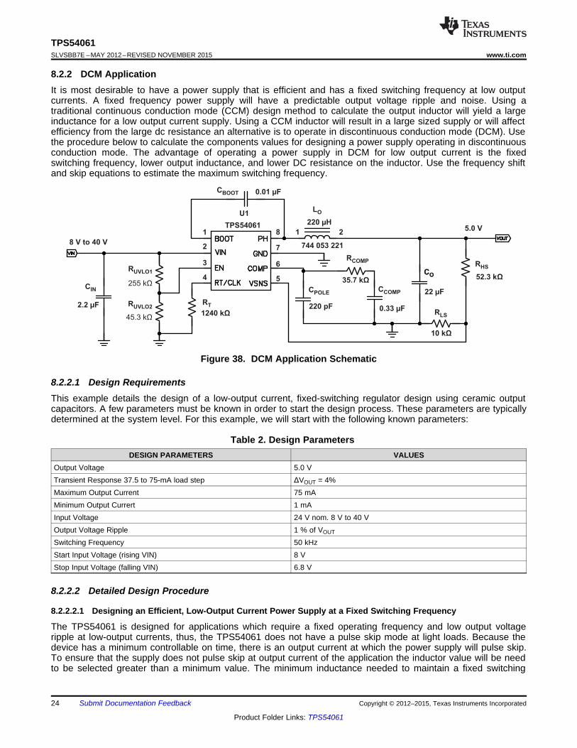
8.2.2 DCM ApplicationIt is most desirable to have a power supply that is efficient and has a fixed switching frequency at low outputcurrents. A fixed frequency power supply will have a predictable output voltage ripple and noise. Using atraditional continuous conduction mode (CCM) design method to calculate the output inductor will yield a largeinductance for a low output current supply. Using a CCM inductor will result in a large sized supply or will affectefficiency from the large dc resistance an alternative is to operate in discontinuous conduction mode (DCM). Usethe procedure below to calculate the components values for designing a power supply operating in discontinuousconduction mode. The advantage of operating a power supply in DCM for low output current is the fixedswitching frequency, lower output inductance, and lower DC resistance on the inductor. Use the frequency shiftand skip equations to estimate the maximum switching frequency.
Figure 38. DCM Application Schematic
8.2.2.1 Design RequirementsThis example details the design of a low-output current, fixed-switching regulator design using ceramic outputcapacitors. A few parameters must be known in order to start the design process. These parameters are typicallydetermined at the system level. For this example, we will start with the following known parameters:
Table 2. Design ParametersDESIGN PARAMETERS VALUES
Output Voltage 5.0 VTransient Response 37.5 to 75-mA load step ΔVOUT = 4%Maximum Output Current 75 mAMinimum Output Currert 1 mAInput Voltage 24 V nom. 8 V to 40 VOutput Voltage Ripple 1 % of VOUT
Switching Frequency 50 kHzStart Input Voltage (rising VIN) 8 VStop Input Voltage (falling VIN) 6.8 V
8.2.2.2 Detailed Design Procedure
8.2.2.2.1 Designing an Efficient, Low-Output Current Power Supply at a Fixed Switching Frequency
The TPS54061 is designed for applications which require a fixed operating frequency and low output voltageripple at low-output currents, thus, the TPS54061 does not have a pulse skip mode at light loads. Because thedevice has a minimum controllable on time, there is an output current at which the power supply will pulse skip.To ensure that the supply does not pulse skip at output current of the application the inductor value will be needto be selected greater than a minimum value. The minimum inductance needed to maintain a fixed switching
24 Submit Documentation Feedback Copyright © 2012–2015, Texas Instruments Incorporated
Product Folder Links: TPS54061

RIPPLEC
L
VR
I peak£
OUT
OUT co
I 1Co3
V³ ´
D f
( )
2 2
O O 2 2
OUT OUT
Io 0C 2 L
V + V V
-³ ´
D -
LO
RIPPLE SW
I peak D1 + D2C 1
V 8 f
æ ö£ ´ ç ÷
´è ø
0.52
CO L
D1 + D2 D1 + D2I rms = I peak
3 4
æ öæ ö æ öç ÷´ -ç ÷ ç ÷ç ÷è ø è øè ø
0.5
L L
D1 + D2I rms = I peak
3
æ ö´ ç ÷
è ø
IN OUT
OUT
V VD2 = D1
V
æ ö-´ç ÷
è ø
( )
0.5
OUT O O sw
IN IN OUT
2 V I LD1 =
V V V
æ ö´ ´ ´ ´ç ÷ç ÷´ -è ø
f
( )0.5
OUT IN OUTL
IN O sw
2 V Iomax V max VI peak =
V max L
æ ö´ ´ ´ -ç ÷ç ÷´ ´è øf
IN OUT OUT
O
IN sw O
V min V V 1L max
2 V min I
æ ö-æ ö£ ´ ´ç ÷ç ÷ ´è ø è ø f
2
IN OUT OIN
o
OUT O
V max V t nminV maxL min sw
V 2 I min
æ ö- æ ö³ ´ ´ç ÷ ç ÷
è øè øx f
TPS54061www.ti.com SLVSBB7E –MAY 2012–REVISED NOVEMBER 2015
frequency at the minimum load is calculated to be 227 µH using Equation 27. Because the equation is ideal andwas derived without losses, assume the minimum controllable light load on time, tonminll, is 180 ns. To maintainDCM operation the inductor value and output current need to stay below a maximum value. The maximuminductance is calculated to be 250 µH using Equation 28. A 744053221 inductor from Würth Elektronik isselected. If CCM operation is necessary, use the previous design procedure.
Use Equation 29, to make sure the minimum current limit on the high-side power switch is not exceeded at themaximum output current. The peak current is calculated as 244 mA and is lower than the 350 mA current limit.To determine the RMS current for the inductor and output capacitor, it is necessary to calculate the duty cycle.The duty cycle, D1, for a step down regulator in DCM is calculated in Equation 30. D1 is the portion of theswitching cycle the high side power switch is on, and is calculated to be 0.1345. D2 is the portion of the switchingcycle the low-side power switch is on, and is calculated to be 0.5111.
Using the Equation 32 and Equation 33, the RMS current of the inductor and output capacitor are calculated, tobe 0.1078 A and 0.0774 A respectively. Select components that ratings exceed the calculated RMS values.Calculate the output capacitance using the Equation 34 to Equation 36 and use the largest value, Vripple is thesteady-state voltage ripple and deltaV is voltage change during a transient. A minimum of 7.5-µF capacitance iscalculated. Additional capacitance de-ratings for aging, temperature and DC bias should be factored in whichincreases this minimum value. For this example, a 22-µF 10-V X7R ceramic capacitor with 5-mΩ ESR is used.To have a low-output ripple power supply use a low ESR capacitor. Use Equation 37 to estimate the maximumESR for the output capacitor. Equation 38 and Equation 39 estimate the RMS current and capacitance for theinput capacitor. An RMS current of 38.7 mA and capacitance of 1.56 µF is calculated. A 2.2-µF 100-V/X7Rceramic is used for this example.
(27)
(28)
(29)
(30)
(31)
(32)
(33)
(34)
(35)
(36)
(37)
Copyright © 2012–2015, Texas Instruments Incorporated Submit Documentation Feedback 25
Product Folder Links: TPS54061

OUTCOMP
POLE REF
VcoR xKdcm Fm V gmea
¦=
´ ´ ¦ ´
( )0.5
CO2 SW POLE(Hz) =f f f´
( )0.5
CO1 ZERO POLE(Hz) =f f f´
ZEROC O
1(Hz) =
R C 2f
p´ ´ ´
OUT
INPOLE
OUT OUTO
O IN
V2
V1(Hz) =
V VC 2 1
I V
f
æ ö-ç ÷
ç ÷´ç ÷
´ ´ ´ -ç ÷è ø
p
IN OUT
O sw
gmpsFm =
V V+ 0.380
L
æ ö-ç ÷
´è øf
( )OUT IN OUT
IN OUTOUT
O
V V V2Kdcm =
D1
RdcV 2 + V
V
I
´ -´
æ öç ÷ç ÷´ -ç ÷ç ÷è ø
ZERO
POLE
s1 +
2Gdcm(s) Fm Kdcm
s1 +
2
f
f
p
p
´ ´
» ´ ´
´ ´
O
IN
IN SW
I 0.25C
V RIPPLE f
æ ö³ ´ ç ÷
è ø
0.52
CIN L
D1 D1I rms = I peak
3 4
æ öæ ö æ öç ÷´ -ç ÷ ç ÷ç ÷è ø è øè ø
TPS54061SLVSBB7E –MAY 2012–REVISED NOVEMBER 2015 www.ti.com
(38)
(39)
8.2.2.2.2 Closing the Feedback Loop
The method presented here is easy to calculate and includes the effect of the slope compensation that is internalto the TPS54061. This method assumes the crossover frequency is between the modulator pole and the ESRzero and the ESR zero is at least 10 times greater than the modulator pole. Once the output components aredetermined, use the equations below to close the feedback loop. A current mode controlled power supplyoperating in DCM has a transfer function which includes an ESR zero and pole as shown in Equation 40. Tocalculate the current mode power stage gain, first calculate, Kdcm, the DCM gain, and Fm, the modulator gain,using Equation 41 and Equation 42. Kdcm and Fm are 32.4 and 0.475 respectively. The location of the pole andESR zero are calculated using Equation 43 and Equation 44 . The pole and zero are 491 Hz and 2.8 MHz,respectively. Use the lower value of Equation 45 and Equation 46 as a starting point for the crossover frequency.Equation 45 is the geometric mean of the power stage pole and the ESR zero and Equation 46 is the mean ofpower stage pole and the switching frequency. The crossover frequency is chosen as 5 kHz from Equation 46.
To determine the compensation resistor, RCOMP, use Equation 47. Assume the power stage transconductance,gmps, is 1.0 A/V. The output voltage, VO, reference voltage, VREF, and amplifier transconductance, gmea, are5.0 V, 0.8 V and 108 µA/V, respectively. RCOMP is calculated to be 38.3 kΩ; use the nearest standard value of35.7 kΩ. Use Equation 48 to set the compensation zero to equalthe modulator pole frequency. Equation 48yields 290 nF for compensating capacitor CCOMP, and a 330 nF is used. Use the larger value of Equation 49 orEquation 50 to calculate the CPOLE, which sets the compensation pole. Equation 50 yields 178 pF standard valueof 220 pF is selected.
(40)
(41)
(42)
(43)
(44)
(45)
(46)
(47)
26 Submit Documentation Feedback Copyright © 2012–2015, Texas Instruments Incorporated
Product Folder Links: TPS54061
0
10
20
30
40
50
60
70
80
90
100
0 0.025 0.05 0.075 0.1
Eff
icie
nc
y (
%)
Load Current (A)
V = 8 VIN
V = 12 VIN
V = 24 VIN
V = 36 VIN
V = 3.3 V,
F = 50 kHzOUT
SW
0
10
20
30
40
50
60
70
80
90
100
0.001 0.01 0.1
Eff
icie
nc
y (
%)
Load Current (A)
V = 8 VIN
V = 12 VIN
V = 24 VIN
V = 36 VIN
V = 3.3 V,
F = 50 kHzOUT
SW
0
10
20
30
40
50
60
70
80
90
100
0.001 0.01 0.1
Eff
icie
nc
y (
%)
Load Current (A)
V = 8 VIN
V = 12 VIN
V = 24 VIN
V = 36 VIN
V = 5 V,
F = 50 kHzOUT
SW
0
10
20
30
40
50
60
70
80
90
100
0 0.025 0.05 0.075 0.1
Eff
icie
ncy (
%)
Load Current (A)
V = 8 VIN
V = 12 VIN
V = 24 VIN
V = 36 VIN
V = 5 V,
F = 50 kHzOUT
SW
POLE2
COMP SW
1C =
R f p´ ´
C O
POLE1
COMP
R CC =
R
´
COMP
COMP
1C =
2 R Kdcm Fmp´ ´ ´ ´
TPS54061www.ti.com SLVSBB7E –MAY 2012–REVISED NOVEMBER 2015
(48)
(49)
(50)
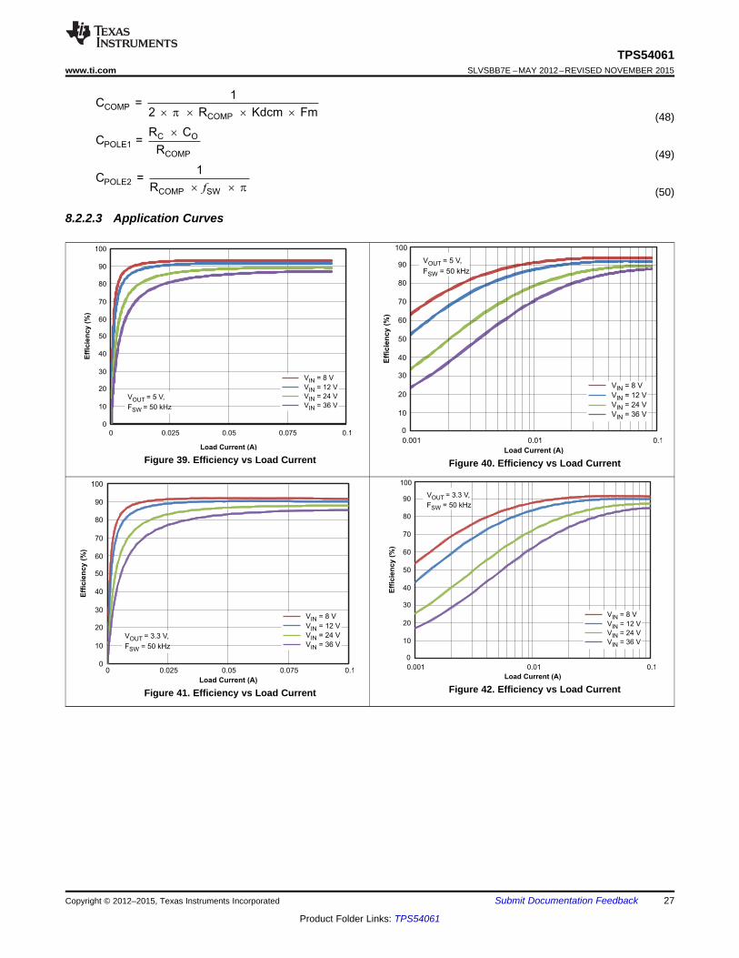
8.2.2.3 Application Curves
Figure 39. Efficiency vs Load Current Figure 40. Efficiency vs Load Current
Figure 42. Efficiency vs Load CurrentFigure 41. Efficiency vs Load Current
Copyright © 2012–2015, Texas Instruments Incorporated Submit Documentation Feedback 27
Product Folder Links: TPS54061
VOUT = 100 mV /div ac coupled
4 ms /div
IOUT = 20 mA/div
EN = 5 V /div
10 ms /div
IOUT
= 50 mA/div
VIN
= 10 V /div
VOUT
= 2 V /div
–0.25
–0.2
–0.15
–0.1
–0.05
0
0.05
0.1
0.15
0.2
0.25
0 10 20 30 40 50 60
Ou
tpu
t V
olt
ag
e N
orm
ali
zed
(%
)
Input Voltage (V)
I = 37.5 mA,
F = 50 kHzOUT
SW
VOUT = 100 mV /div ac coupled
2 ms /div
IOUT = 20 mA/div
VOUT = 100 mV /div ac coupled
2 ms /div
IOUT = 20 mA/div
10 100 1K 10K 100K
–180
–90
0
45
90
135
180
Ga
in (
dB
)
Frequency (Hz)
Ph
as
e (
º)
–45
Gain
Phase
–135
–40
–20
0
10
20
30
40
–10
–30
–0.50
–0.40
–0.30
–0.20
–0.10
0.00
0.10
0.20
0.30
0.40
0.50
0 0.025 0.05 0.075 0.1
Ou
tpu
t V
olt
ag
e N
orm
ali
zed
(%
)
Load Current (A)
V = 24 V,
V = 5 V,
F = 50 kHz
IN
OUT
SW
TPS54061SLVSBB7E –MAY 2012–REVISED NOVEMBER 2015 www.ti.com
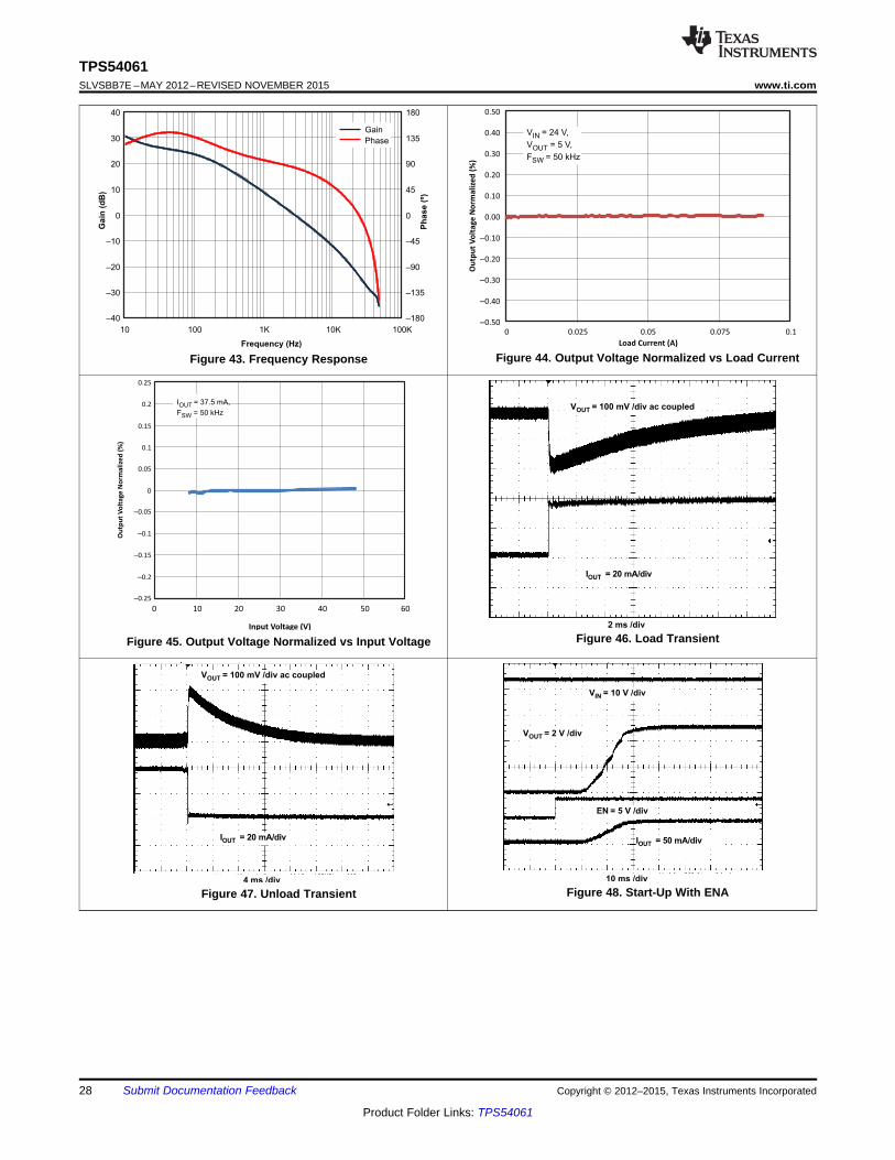
Figure 44. Output Voltage Normalized vs Load CurrentFigure 43. Frequency Response
Figure 46. Load TransientFigure 45. Output Voltage Normalized vs Input Voltage
Figure 48. Start-Up With ENAFigure 47. Unload Transient
28 Submit Documentation Feedback Copyright © 2012–2015, Texas Instruments Incorporated
Product Folder Links: TPS54061

PH = 20 V /div
VOUT = 20 mV /div ac coupled
4 s /divµ
VIN = 20 mV /div ac coupled
Inductor current = 20 mA/div
PH = 20 V /div
VOUT = 50 mV /div ac coupled
4 s /divµ
VIN = 100 nV /div ac coupled
Inductor current = 100 mA/div
EN = 5 V /div
10 ms /div
IOUT
= 50 mA/div
VIN
= 10 V /div
VOUT
= 2 V /div
EN = 5 V /div
10 ms /div
IOUT
= 50 mA/div
VIN
= 10 V /div
VOUT
= 2 V /div
EN = 5 V /div
10 ms /div
IOUT
= 50 mA/div
VIN
= 10 V /div
VOUT
= 2 V /div
TPS54061www.ti.com SLVSBB7E –MAY 2012–REVISED NOVEMBER 2015
Figure 50. Prebias Start-Up With ENAFigure 49. Start-Up With VIN
Figure 51. Prebias Start-Up With VIN Figure 52. Input and Output Ripple in DCM
Figure 53. Input and Output Ripple in PSM
Copyright © 2012–2015, Texas Instruments Incorporated Submit Documentation Feedback 29
Product Folder Links: TPS54061

VSENSE
COMP
GND
PHBOOT
VIN
EN
RT/CLK
Frequency Set
Resistor
Boot
Capacitor
Input
Capacitor
Output
Capacitor
VOUT
Output
Inductor
Compensation
Network
Feedback
ResistorsUVLO
Adjust
Resistor
VIN
GND
Route Boot Capacitor
Trace on another layer to
provide wide path for
topside ground
Signal VIA
TPS54061SLVSBB7E –MAY 2012–REVISED NOVEMBER 2015 www.ti.com
9 Power Supply RecommendationsThe TPS54061 is designed to operate from an input voltage supply range between 4.7 V and 60 V. This inputsupply should remain within the input voltage supply range. If the input supply is located more than a few inchesfrom the TPS54061 converter bulk capacitance may be required in addition to the ceramic bypass capacitors.
10 Layout
10.1 Layout GuidelinesLayout is a critical portion of good power supply design. There are several signals paths that conduct fastchanging currents or voltages that can interact with stray inductance or parasitic capacitance to generate noiseor degrade the power supplies performance. To help eliminate these problems, the VIN pin should be bypassedto ground with a low-ESR ceramic bypass capacitor with X5R or X7R dielectric. Take care to minimize the looparea formed by the bypass capacitor connections, the VIN pin, and the GND pin. See Figure 54 for a PCB layoutexample. Because the PH connection is the switching node and output inductor should be located close to thePH pins, and the area of the PCB conductor minimized to prevent excessive capacitive coupling. The RT/CLKpin is sensitive to noise. so the RT resistor should be located as close as possible to the IC and routed withminimal lengths of trace. The additional external components can be placed approximately as shown. It may bepossible to obtain acceptable performance with alternate PCB layouts; however; this layout has been shown toproduce good results and is meant as a guideline.
10.2 Layout Example
Figure 54. PCB Layout Example
30 Submit Documentation Feedback Copyright © 2012–2015, Texas Instruments Incorporated
Product Folder Links: TPS54061
TPS54061www.ti.com SLVSBB7E –MAY 2012–REVISED NOVEMBER 2015
11 Device and Documentation Support
11.1 TrademarksWEBENCH is a trademark of Texas Instruments.All other trademarks are the property of their respective owners.
11.2 Electrostatic Discharge CautionThese devices have limited built-in ESD protection. The leads should be shorted together or the device placed in conductive foamduring storage or handling to prevent electrostatic damage to the MOS gates.
11.3 GlossarySLYZ022 — TI Glossary.
This glossary lists and explains terms, acronyms, and definitions.
12 Mechanical, Packaging, and Orderable InformationThe following pages include mechanical, packaging, and orderable information. This information is the mostcurrent data available for the designated devices. This data is subject to change without notice and revision ofthis document. For browser-based versions of this data sheet, refer to the left-hand navigation.
Copyright © 2012–2015, Texas Instruments Incorporated Submit Documentation Feedback 31
Product Folder Links: TPS54061

PACKAGE OPTION ADDENDUM
www.ti.com 12-Oct-2015
Addendum-Page 1
PACKAGING INFORMATION
Orderable Device Status(1)
Package Type PackageDrawing
Pins PackageQty
Eco Plan(2)
Lead/Ball Finish(6)
MSL Peak Temp(3)
Op Temp (°C) Device Marking(4/5)
Samples
TPS54061DRBR ACTIVE SON DRB 8 3000 Green (RoHS& no Sb/Br)
CU NIPDAU Level-2-260C-1 YEAR -40 to 150 61
TPS54061DRBT ACTIVE SON DRB 8 250 Green (RoHS& no Sb/Br)
CU NIPDAU Level-2-260C-1 YEAR -40 to 150 61
(1) The marketing status values are defined as follows:ACTIVE: Product device recommended for new designs.LIFEBUY: TI has announced that the device will be discontinued, and a lifetime-buy period is in effect.NRND: Not recommended for new designs. Device is in production to support existing customers, but TI does not recommend using this part in a new design.PREVIEW: Device has been announced but is not in production. Samples may or may not be available.OBSOLETE: TI has discontinued the production of the device.
(2) Eco Plan - The planned eco-friendly classification: Pb-Free (RoHS), Pb-Free (RoHS Exempt), or Green (RoHS & no Sb/Br) - please check http://www.ti.com/productcontent for the latest availabilityinformation and additional product content details.TBD: The Pb-Free/Green conversion plan has not been defined.Pb-Free (RoHS): TI's terms "Lead-Free" or "Pb-Free" mean semiconductor products that are compatible with the current RoHS requirements for all 6 substances, including the requirement thatlead not exceed 0.1% by weight in homogeneous materials. Where designed to be soldered at high temperatures, TI Pb-Free products are suitable for use in specified lead-free processes.Pb-Free (RoHS Exempt): This component has a RoHS exemption for either 1) lead-based flip-chip solder bumps used between the die and package, or 2) lead-based die adhesive used betweenthe die and leadframe. The component is otherwise considered Pb-Free (RoHS compatible) as defined above.Green (RoHS & no Sb/Br): TI defines "Green" to mean Pb-Free (RoHS compatible), and free of Bromine (Br) and Antimony (Sb) based flame retardants (Br or Sb do not exceed 0.1% by weightin homogeneous material)
(3) MSL, Peak Temp. - The Moisture Sensitivity Level rating according to the JEDEC industry standard classifications, and peak solder temperature.
(4) There may be additional marking, which relates to the logo, the lot trace code information, or the environmental category on the device.
(5) Multiple Device Markings will be inside parentheses. Only one Device Marking contained in parentheses and separated by a "~" will appear on a device. If a line is indented then it is a continuationof the previous line and the two combined represent the entire Device Marking for that device.
(6) Lead/Ball Finish - Orderable Devices may have multiple material finish options. Finish options are separated by a vertical ruled line. Lead/Ball Finish values may wrap to two lines if the finishvalue exceeds the maximum column width.
Important Information and Disclaimer:The information provided on this page represents TI's knowledge and belief as of the date that it is provided. TI bases its knowledge and belief on informationprovided by third parties, and makes no representation or warranty as to the accuracy of such information. Efforts are underway to better integrate information from third parties. TI has taken andcontinues to take reasonable steps to provide representative and accurate information but may not have conducted destructive testing or chemical analysis on incoming materials and chemicals.TI and TI suppliers consider certain information to be proprietary, and thus CAS numbers and other limited information may not be available for release.

PACKAGE OPTION ADDENDUM
www.ti.com 12-Oct-2015
Addendum-Page 2
In no event shall TI's liability arising out of such information exceed the total purchase price of the TI part(s) at issue in this document sold by TI to Customer on an annual basis.
OTHER QUALIFIED VERSIONS OF TPS54061 :
• Automotive: TPS54061-Q1
NOTE: Qualified Version Definitions:
• Automotive - Q100 devices qualified for high-reliability automotive applications targeting zero defects
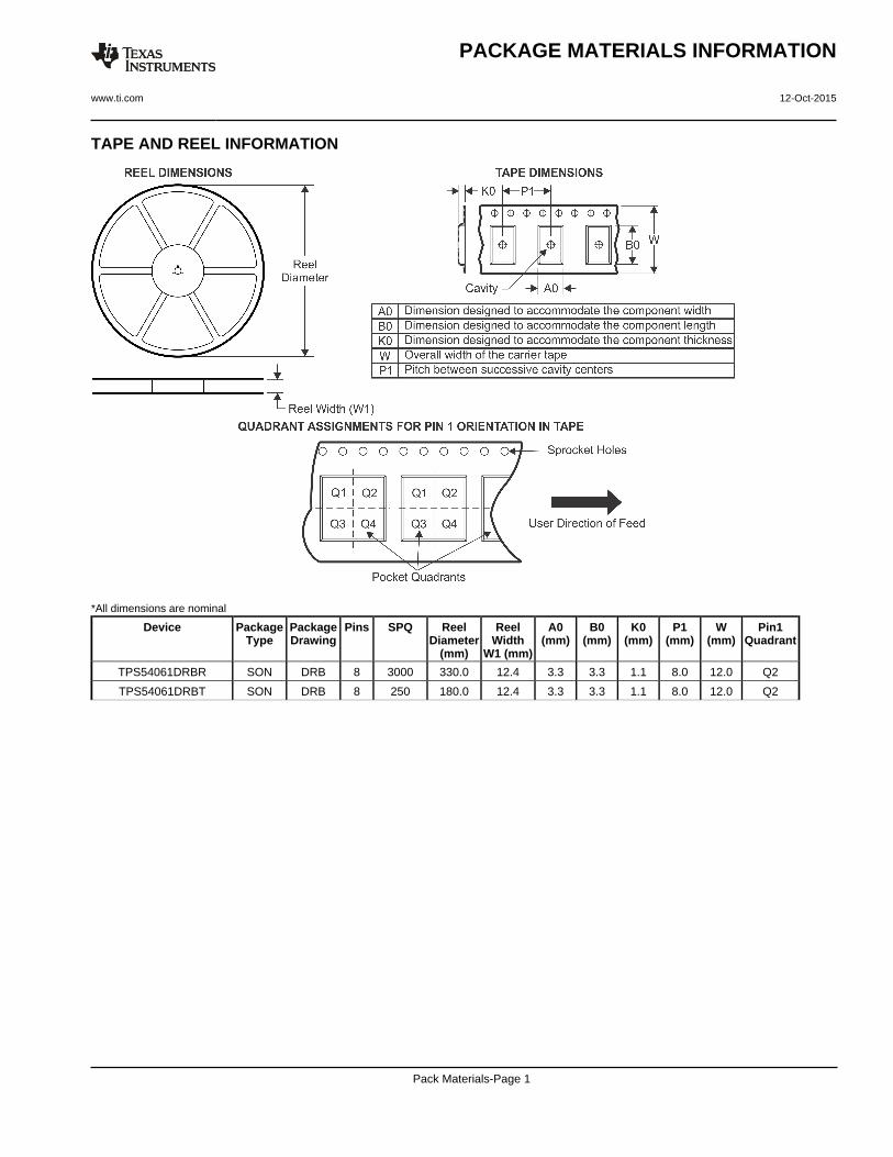
TAPE AND REEL INFORMATION
*All dimensions are nominal
Device PackageType
PackageDrawing
Pins SPQ ReelDiameter
(mm)
ReelWidth
W1 (mm)
A0(mm)
B0(mm)
K0(mm)
P1(mm)
W(mm)
Pin1Quadrant
TPS54061DRBR SON DRB 8 3000 330.0 12.4 3.3 3.3 1.1 8.0 12.0 Q2
TPS54061DRBT SON DRB 8 250 180.0 12.4 3.3 3.3 1.1 8.0 12.0 Q2
PACKAGE MATERIALS INFORMATION
www.ti.com 12-Oct-2015
Pack Materials-Page 1
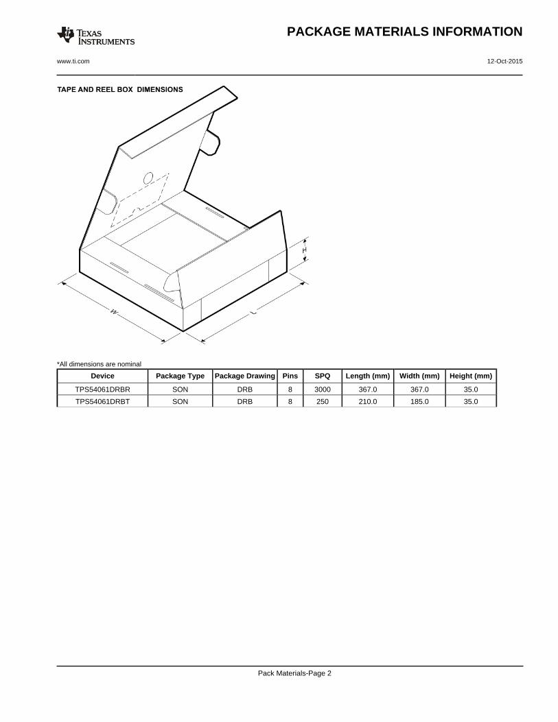
*All dimensions are nominal
Device Package Type Package Drawing Pins SPQ Length (mm) Width (mm) Height (mm)
TPS54061DRBR SON DRB 8 3000 367.0 367.0 35.0
TPS54061DRBT SON DRB 8 250 210.0 185.0 35.0
PACKAGE MATERIALS INFORMATION
www.ti.com 12-Oct-2015
Pack Materials-Page 2


www.ti.com
PACKAGE OUTLINE
C
8X 0.350.25
2.4 0.052X
1.95
1.65 0.05
6X 0.65
1 MAX
8X 0.50.3
0.050.00
A 3.12.9
B
3.12.9
(0.2) TYP
VSON - 1 mm max heightDRB0008BPLASTIC SMALL OUTLINE - NO LEAD
4218876/A 12/2017
PIN 1 INDEX AREA
SEATING PLANE
0.08 C
1
4 5
8
(OPTIONAL)PIN 1 ID 0.1 C A B
0.05 C
THERMAL PADEXPOSED
NOTES: 1. All linear dimensions are in millimeters. Any dimensions in parenthesis are for reference only. Dimensioning and tolerancing per ASME Y14.5M. 2. This drawing is subject to change without notice. 3. The package thermal pad must be soldered to the printed circuit board for thermal and mechanical performance.
SCALE 4.000

www.ti.com
EXAMPLE BOARD LAYOUT
0.07 MINALL AROUND
0.07 MAXALL AROUND
8X (0.3)
(2.4)
(2.8)
6X (0.65)
(1.65)
( 0.2) VIATYP
(0.575)
(0.95)
8X (0.6)
(R0.05) TYP
VSON - 1 mm max heightDRB0008BPLASTIC SMALL OUTLINE - NO LEAD
4218876/A 12/2017
SYMM
1
45
8
LAND PATTERN EXAMPLESCALE:20X
NOTES: (continued) 4. This package is designed to be soldered to a thermal pad on the board. For more information, see Texas Instruments literature number SLUA271 (www.ti.com/lit/slua271).5. Vias are optional depending on application, refer to device data sheet. If any vias are implemented, refer to their locations shown on this view. It is recommended that vias under paste be filled, plugged or tented.
SOLDER MASKOPENINGSOLDER MASK
METAL UNDER
SOLDER MASKDEFINED
METALSOLDER MASKOPENING
SOLDER MASK DETAILS
NON SOLDER MASKDEFINED
(PREFERRED)
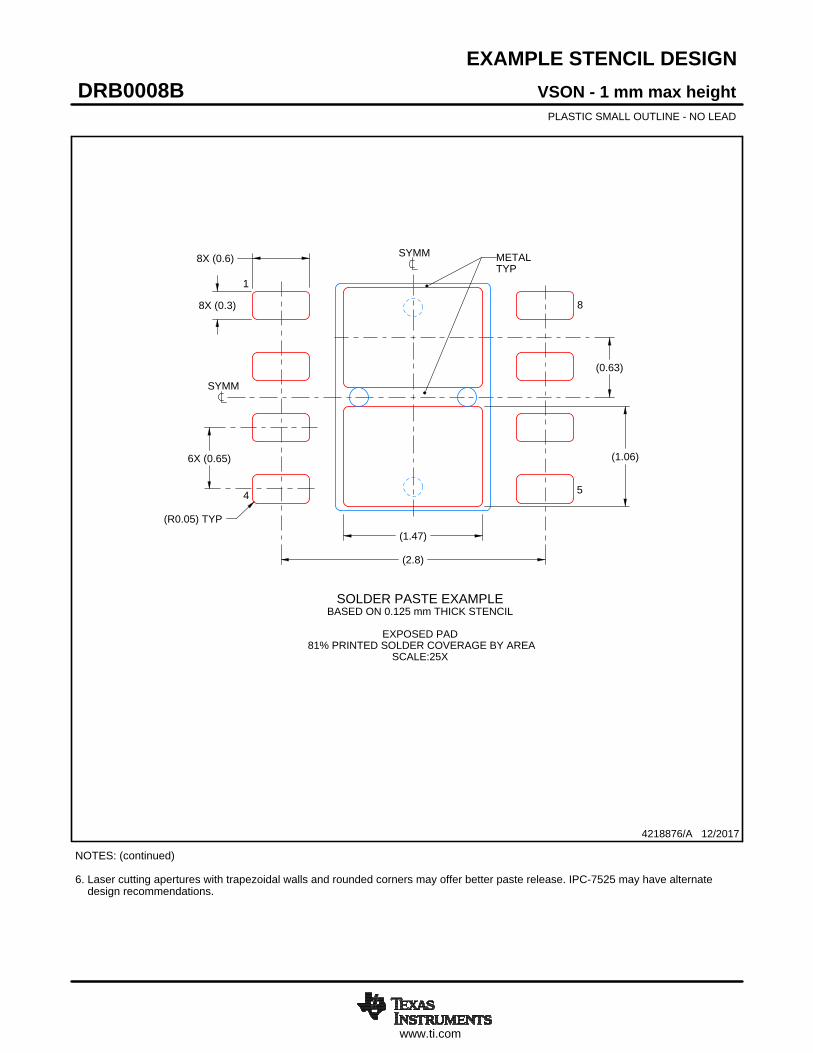
www.ti.com
EXAMPLE STENCIL DESIGN
(R0.05) TYP
8X (0.3)
8X (0.6)
(1.47)
(1.06)
(2.8)
(0.63)
6X (0.65)
VSON - 1 mm max heightDRB0008BPLASTIC SMALL OUTLINE - NO LEAD
4218876/A 12/2017
NOTES: (continued) 6. Laser cutting apertures with trapezoidal walls and rounded corners may offer better paste release. IPC-7525 may have alternate design recommendations.
SOLDER PASTE EXAMPLEBASED ON 0.125 mm THICK STENCIL
EXPOSED PAD
81% PRINTED SOLDER COVERAGE BY AREASCALE:25X
SYMM
1
4 5
8
METALTYP
SYMM
IMPORTANT NOTICE
Texas Instruments Incorporated (TI) reserves the right to make corrections, enhancements, improvements and other changes to itssemiconductor products and services per JESD46, latest issue, and to discontinue any product or service per JESD48, latest issue. Buyersshould obtain the latest relevant information before placing orders and should verify that such information is current and complete.TI’s published terms of sale for semiconductor products (http://www.ti.com/sc/docs/stdterms.htm) apply to the sale of packaged integratedcircuit products that TI has qualified and released to market. Additional terms may apply to the use or sale of other types of TI products andservices.Reproduction of significant portions of TI information in TI data sheets is permissible only if reproduction is without alteration and isaccompanied by all associated warranties, conditions, limitations, and notices. TI is not responsible or liable for such reproduceddocumentation. Information of third parties may be subject to additional restrictions. Resale of TI products or services with statementsdifferent from or beyond the parameters stated by TI for that product or service voids all express and any implied warranties for theassociated TI product or service and is an unfair and deceptive business practice. TI is not responsible or liable for any such statements.Buyers and others who are developing systems that incorporate TI products (collectively, “Designers”) understand and agree that Designersremain responsible for using their independent analysis, evaluation and judgment in designing their applications and that Designers havefull and exclusive responsibility to assure the safety of Designers' applications and compliance of their applications (and of all TI productsused in or for Designers’ applications) with all applicable regulations, laws and other applicable requirements. Designer represents that, withrespect to their applications, Designer has all the necessary expertise to create and implement safeguards that (1) anticipate dangerousconsequences of failures, (2) monitor failures and their consequences, and (3) lessen the likelihood of failures that might cause harm andtake appropriate actions. Designer agrees that prior to using or distributing any applications that include TI products, Designer willthoroughly test such applications and the functionality of such TI products as used in such applications.TI’s provision of technical, application or other design advice, quality characterization, reliability data or other services or information,including, but not limited to, reference designs and materials relating to evaluation modules, (collectively, “TI Resources”) are intended toassist designers who are developing applications that incorporate TI products; by downloading, accessing or using TI Resources in anyway, Designer (individually or, if Designer is acting on behalf of a company, Designer’s company) agrees to use any particular TI Resourcesolely for this purpose and subject to the terms of this Notice.TI’s provision of TI Resources does not expand or otherwise alter TI’s applicable published warranties or warranty disclaimers for TIproducts, and no additional obligations or liabilities arise from TI providing such TI Resources. TI reserves the right to make corrections,enhancements, improvements and other changes to its TI Resources. TI has not conducted any testing other than that specificallydescribed in the published documentation for a particular TI Resource.Designer is authorized to use, copy and modify any individual TI Resource only in connection with the development of applications thatinclude the TI product(s) identified in such TI Resource. NO OTHER LICENSE, EXPRESS OR IMPLIED, BY ESTOPPEL OR OTHERWISETO ANY OTHER TI INTELLECTUAL PROPERTY RIGHT, AND NO LICENSE TO ANY TECHNOLOGY OR INTELLECTUAL PROPERTYRIGHT OF TI OR ANY THIRD PARTY IS GRANTED HEREIN, including but not limited to any patent right, copyright, mask work right, orother intellectual property right relating to any combination, machine, or process in which TI products or services are used. Informationregarding or referencing third-party products or services does not constitute a license to use such products or services, or a warranty orendorsement thereof. Use of TI Resources may require a license from a third party under the patents or other intellectual property of thethird party, or a license from TI under the patents or other intellectual property of TI.TI RESOURCES ARE PROVIDED “AS IS” AND WITH ALL FAULTS. TI DISCLAIMS ALL OTHER WARRANTIES ORREPRESENTATIONS, EXPRESS OR IMPLIED, REGARDING RESOURCES OR USE THEREOF, INCLUDING BUT NOT LIMITED TOACCURACY OR COMPLETENESS, TITLE, ANY EPIDEMIC FAILURE WARRANTY AND ANY IMPLIED WARRANTIES OFMERCHANTABILITY, FITNESS FOR A PARTICULAR PURPOSE, AND NON-INFRINGEMENT OF ANY THIRD PARTY INTELLECTUALPROPERTY RIGHTS. TI SHALL NOT BE LIABLE FOR AND SHALL NOT DEFEND OR INDEMNIFY DESIGNER AGAINST ANY CLAIM,INCLUDING BUT NOT LIMITED TO ANY INFRINGEMENT CLAIM THAT RELATES TO OR IS BASED ON ANY COMBINATION OFPRODUCTS EVEN IF DESCRIBED IN TI RESOURCES OR OTHERWISE. IN NO EVENT SHALL TI BE LIABLE FOR ANY ACTUAL,DIRECT, SPECIAL, COLLATERAL, INDIRECT, PUNITIVE, INCIDENTAL, CONSEQUENTIAL OR EXEMPLARY DAMAGES INCONNECTION WITH OR ARISING OUT OF TI RESOURCES OR USE THEREOF, AND REGARDLESS OF WHETHER TI HAS BEENADVISED OF THE POSSIBILITY OF SUCH DAMAGES.Unless TI has explicitly designated an individual product as meeting the requirements of a particular industry standard (e.g., ISO/TS 16949and ISO 26262), TI is not responsible for any failure to meet such industry standard requirements.Where TI specifically promotes products as facilitating functional safety or as compliant with industry functional safety standards, suchproducts are intended to help enable customers to design and create their own applications that meet applicable functional safety standardsand requirements. Using products in an application does not by itself establish any safety features in the application. Designers mustensure compliance with safety-related requirements and standards applicable to their applications. Designer may not use any TI products inlife-critical medical equipment unless authorized officers of the parties have executed a special contract specifically governing such use.Life-critical medical equipment is medical equipment where failure of such equipment would cause serious bodily injury or death (e.g., lifesupport, pacemakers, defibrillators, heart pumps, neurostimulators, and implantables). Such equipment includes, without limitation, allmedical devices identified by the U.S. Food and Drug Administration as Class III devices and equivalent classifications outside the U.S.TI may expressly designate certain products as completing a particular qualification (e.g., Q100, Military Grade, or Enhanced Product).Designers agree that it has the necessary expertise to select the product with the appropriate qualification designation for their applicationsand that proper product selection is at Designers’ own risk. Designers are solely responsible for compliance with all legal and regulatoryrequirements in connection with such selection.Designer will fully indemnify TI and its representatives against any damages, costs, losses, and/or liabilities arising out of Designer’s non-compliance with the terms and provisions of this Notice.
Mailing Address: Texas Instruments, Post Office Box 655303, Dallas, Texas 75265Copyright © 2018, Texas Instruments Incorporated