Embed Size (px)
Citation preview

Using the TPS40140EVM-003
User's Guide
Literature Number: SLVU219A
August 2007–Revised November 2010
User's GuideSLVU219A–August 2007–Revised November 2010
Using the TPS40140EVM-003 A 32-A Single OutputTwo-Phase Stackable Synchronous Buck Converter
The TPS40140EVM-003 evaluation module (EVM) is a single output two-phase synchronous buckconverter. The EVM delivers 1.5 V at 32 A. The module uses the TPS40140 dual or 2-phase stackablesynchronous buck controller. The EVM is also stackable with the other EVM to construct a multiphaseconverter.
1 Description
TPS40140EVM-003 is designed to use a regulated 10.8-V to 13.2-V bus to produce high-current regulatedoutput. The TPS40140EVM-003 evaluation module demonstrates the TPS40140 in a typical regulated busto low-voltage application while providing a number of test points to evaluate the performance of theTPS40140 in a given application.
1.1 Applications• Graphics Cards• Internet Servers• Networking Equipment• Telecommunications Equipment• DC Power Distributed Systems
1.2 Features• 10.8-V to 13.2-V Input Range• 1.5-V Fixed Output• 32-ADC Steady State Current per Output• 300-kHz Switching Frequency per Phase• Single Main Switch N-channel MOSFET and Two Synchronous Rectifier N-channel MOSFETs per
Phase• Convenient Test Points for Probing Critical Waveforms and Non-Invasive Loop Response Testing
2 Using the TPS40140EVM-003 A 32-A Single Output Two-Phase Stackable SLVU219A–August 2007–Revised November 2010Synchronous Buck Converter Submit Documentation Feedback
Copyright © 2007–2010, Texas Instruments Incorporated

www.ti.com TPS40140EVM-003 Electrical Performance Specifications
2 TPS40140EVM-003 Electrical Performance Specifications
Table 1. TPS40140EVM-003 Electrical and Performance Specifications
PARAMETER CONDITIONS MIN TYP MAX UNIT
Input Characteristics
Input Voltage Range 10.8 13.2 V
Max Input Current VIN = 10.8 V, IOUT = 32 A 4.98 A
No-Load Input Current VIN = 13.2 V, IOUT = 0 A 130 mA
Output Characteristics (VOUT)
Output Voltage 1.51 V
Line Regulation (10.8 V <VIN <13.2 V, IOUT = 10 A) 0.1%Output Voltage Regulation
Load Regulation (0A <IOUT <32 A, VIN = 12 V) 0.5%
Output Voltage Ripple VIN = 13.2 V, IOUT = 32 A 40 mVpp
Output Load Current IOUT 0 32 A
Output Over Current 40 A
System Characteristics
Switching Frequency 300 kHz
Peak Efficiency VOUT = 1.5 V, IOUT = 20 A, VIN = 10.8 V 91%
Full Load Efficiency VOUT = 1.5 V, IOUT = 32 A, VIN = 12 V 89.9%
3SLVU219A–August 2007–Revised November 2010 Using the TPS40140EVM-003 A 32-A Single Output Two-Phase StackableSynchronous Buck ConverterSubmit Documentation Feedback
Copyright © 2007–2010, Texas Instruments Incorporated

++
++
Schematic www.ti.com
3 Schematic
Figure 1. TPS40140EVM-003 Schematic(for reference only, see List of Materials for specific values)
4 Using the TPS40140EVM-003 A 32-A Single Output Two-Phase Stackable SLVU219A–August 2007–Revised November 2010Synchronous Buck Converter Submit Documentation Feedback
Copyright © 2007–2010, Texas Instruments Incorporated

www.ti.com Test Set Up
4 Test Set Up
4.1 Recommended Test Equipment
4.1.1 Voltage Source
VIN
The input voltage source (VIN) should be a 0 V to 15V variable DC source capable of 10 ADC. Connect VINto J1 as shown in Figure 2.
4.1.2 Meters
V1: VIN, 0 V to 15V voltmeterV2: VOUT, 0 V to 5V voltmeterI1: 0 V to 10A current meter
4.1.3 Load
LOADThe Output Load (LOAD) should be an Electronic Constant Current Mode Load capable of 0–40Adc at1.5V
4.1.4 Oscilloscope
A Digital or Analog Oscilloscope can be used to measure the ripple voltage on VOUT. The Oscilloscopeshould be set for 1MΩ impedance, 20MHz Bandwidth, AC coupling, 1ms/division horizontal resolution,10mV/division vertical resolution for taking output ripple measurements. Test points TP9 and TP10 can beused to measure the output ripple voltage by placing the oscilloscope probe tip through TP9 and holdingthe ground barrel to TP10 as shown in Figure 3. Using a leaded ground connection may induce additionalnoise due to the large ground loop area.
4.1.5 Recommended Wire Gauge
VIN to J1The connection between the source voltage, VIN and J1 of the EVM can carry as much as 6 Amps DC.The minimum recommended wire size is 1x AWG #16 per input connection, with the total length of wireless than 4 feet (2 feet input, 2 feet return).
J3, J4 to LOAD (Power)The power connection between J3 and J4 of the EVM and LOAD can carry as much as 32Adc. Theminimum recommended wire size is 2x AWG #14, with the total length of wire less than 4 feet (2 feetoutput, 2 feet return).
5SLVU219A–August 2007–Revised November 2010 Using the TPS40140EVM-003 A 32-A Single Output Two-Phase StackableSynchronous Buck ConverterSubmit Documentation Feedback
Copyright © 2007–2010, Texas Instruments Incorporated

Test Set Up www.ti.com
4.1.6 Other
FANThis evaluation module includes components that can get hot to the touch, because this EVM is notenclosed to allow probing of circuit nodes, a small fan capable of 200-400 lfm is required to reducecomponent surface temperatures to prevent user injury. The EVM should not be left unattended whilepowered. The EVM should not be probed while the fan is not running.
4.2 Equipment Setup
Shown in Figure 2 is the basic test set up recommended to evaluate the TPS40140EVM-003.
Working at an ESD workstation, make sure that any wrist straps, bootstraps or mats are connectedreferencing the user to earth ground before power is applied to the EVM. Electrostatic smock and safetyglasses should also be worn.
4.2.1 Input Connections1. Prior to connecting the DC input source, VIN, it is advisable to limit the source current from VIN to 6A
maximum. Make sure VIN is initially set to 0V and connected as shown in Figure 2.
4.2.2 Output Connections1. Connect LOAD to J3 and J4, set LOAD to constant current mode to sink 0 Adc before VIN is applied.2. Connect voltmeter, V2, across TP9 and TP10, as shown in Figure 2.
4.2.3 Other Connections1. Place Fan as shown in Figure 2 and turn on, making sure air is flowing across the EVM.
6 Using the TPS40140EVM-003 A 32-A Single Output Two-Phase Stackable SLVU219A–August 2007–Revised November 2010Synchronous Buck Converter Submit Documentation Feedback
Copyright © 2007–2010, Texas Instruments Incorporated

FA
N
Vin
I1
+ -V1
-+
LO
AD
V2
+- + _
www.ti.com Test Set Up
4.2.4 Set Up Diagram
Figure 2. TPS40140EVM-003 Recommended Test Set-Up
7SLVU219A–August 2007–Revised November 2010 Using the TPS40140EVM-003 A 32-A Single Output Two-Phase StackableSynchronous Buck ConverterSubmit Documentation Feedback
Copyright © 2007–2010, Texas Instruments Incorporated

Metal Ground Barrel
Probe Tip
TP9 TP10
Tip and Barrel Output Ripple Measurement
÷ø
öçè
æ´
ChannelA
ChannelBLOG20
Test Set Up www.ti.com
Figure 3. Output Ripple Measurement
4.3 Start Up and Test Procedure1. Ensure LOAD is set to constant current mode and to sink 0 Adc.2. Increase VIN from 0 V to 10.8 Vdc, VOUT should be in regulation per Table 1. Continue increasing VIN to
12 V.3. Vary LOAD from 0 to 32 Adc, VOUT should remain in regulation per Table 1.4. Vary VIN from 10.8 Vdc to 13.2 Vdc, VOUT should remain in regulation per Table 1.5. For various VIN settings vary LOAD from 0 to 32 Adc. VOUT should remain in regulation per Table 1 for
all combinations of load on LOAD up to 32 A.
4.4 Control Loop Gain and Phase Measurement Procedure1. Connect 1 kHz–1 MHz Isolation Transformer to test points marked CHA and CHB.2. Connect Input Signal Amplitude Measurement Probe (Channel A) to CHA.3. Connect Output Signal Amplitude Measurement Probe (Channel B) to CHB.4. Connect Ground Lead of Channel A and Channel B to AGND5. Inject 25 mV or less signal through the Isolation Transformer.6. Sweep Frequency from 100 Hz to 1 MHz with 10 Hz or lower post filter.
7. Control Loop Gain can be measured by8. Control Loop Phase is measured by the Phase difference between Channel A and Channel B.9. Disconnect Isolation Transformer from the bode plot test points before making other measurements
(Signal Injection into Feedback may interfere with accuracy of other measurements).
8 Using the TPS40140EVM-003 A 32-A Single Output Two-Phase Stackable SLVU219A–August 2007–Revised November 2010Synchronous Buck Converter Submit Documentation Feedback
Copyright © 2007–2010, Texas Instruments Incorporated

JP1
JP2
JP3
JP4
JP5
TRK1
RT
UVLO
PSELIN
ILIM1
JP1
JP2
JP3
JP4
JP5
TRK1
RT
UVLO
PSELIN
ILIM1
JP1
JP2
JP3
JP4
JP5
TRK1
RT
UVLO
PSELIN
ILIM1
www.ti.com Test Set Up
4.5 EVM Configuration
4.5.1 Two Phase Single Output Configuration (Default)
Figure 4. Default Configuration
JP4 is shorted with a jumper and others are left open. In this configuration, the EVM operates as a twophase single output converter.
4.5.2 Disabling the Output
JP3 allows the user to disable or enable the output. The output is disabled by shorting JP3 with a Jumper.
Figure 5. Output Disable Configuration
4.5.3 Multiphase Configuration
This EVM is stackable with other identical boards. For example, two EVMs can construct a fullyinterleaved four phase converter. In Figure 6, the EVM is configured as a master while stacking with theother EVM board.
Figure 6. Configure the EVM as a Master for Stackable Operation
9SLVU219A–August 2007–Revised November 2010 Using the TPS40140EVM-003 A 32-A Single Output Two-Phase StackableSynchronous Buck ConverterSubmit Documentation Feedback
Copyright © 2007–2010, Texas Instruments Incorporated

JP1
JP2
JP3
JP4
JP5
TRK1
RT
UVLO
PSELIN
ILIM1
Supplied 2mm male-to-male header
CLKIO
AGND
PHSELOUT
AGND
AGND
COMP
AGND
PHSELIN
AGND
AGND
COMP
AGND
MASTER SLAVE1
AGND
PHSELOUT
AGND
AGND
COMP
CLKIOCLKIO
AGNDAGND
AGND AGND AGND
AGND
PHSELIN
AGND
AGND
COMP
AGND
SLAVE2
AGND
PHSELOUT
AGND
AGND
COMP
CLKIOCLKIO
AGND
AGND AGND
J6 J5
J6 J5
J6
Test Set Up www.ti.com
If two EVM boards are stacked together, the other EVM is configured as a slave as shown in Figure 7.
Figure 7. Configure the EVM as a Slave for Stackable Operation
If more than two EVM boards are stacked, for example three, the two slave EVMs have slightly differentsettings. Considering the master is the first board in the chain and all others are slaves, JP4 in the lastslave board should be shorted by a jumper while it is left as open in other slave boards. Theconfigurations are shown in Figure 8.
Figure 8. Master and Slave Connection (this EVM is the slave)
J5 and J6 are used to connect the EVM to the other EVM boards. Male-to-male headers are provided tomake the connections between the boards.
10 Using the TPS40140EVM-003 A 32-A Single Output Two-Phase Stackable SLVU219A–August 2007–Revised November 2010Synchronous Buck Converter Submit Documentation Feedback
Copyright © 2007–2010, Texas Instruments Incorporated

www.ti.com Test Set Up
4.6 Test Points
Several test points are located around the board. These can be used to sense what is occurring atdifferent points of the converter. Table 2 lists these test points and what they are used for.
Table 2. List of Test Points
NAME TEST POINT LABEL DESCRIPTION
TP1 VIN Input voltage positive sense point
TP2 PGND Input voltage negative sense point
TP3 TRK1 Soft Start
TP4 SW1 Channel 1 switch node
TP5 COMP Error amplifier output
TP6 PGOOD Power Good
TP7 CHA Loop injection point CHA
TP8 CHB Loop injection point CHB
TP9 VOUT Output positive sense point
TP10 PGND Output negative sense point
TP11 SW2 Channel 2 switch node
TP12 AGND Analog Ground
TP13 AGND Analog Ground
4.7 Equipment Shutdown1. Shut down LOAD2. Shut down VIN
3. Shut down FAN
11SLVU219A–August 2007–Revised November 2010 Using the TPS40140EVM-003 A 32-A Single Output Two-Phase StackableSynchronous Buck ConverterSubmit Documentation Feedback
Copyright © 2007–2010, Texas Instruments Incorporated

0 5 10 20 25 30 35
Load Current (A)
0
20
40
60
80
100
15
10
30
50
70
90
Eff
icie
nc
y(%
)
10.8
12.0
13.2
EFFICIENCY
vs
LOAD CURRENT
0 5 10 20 25 30 35
Load Current (A)
0
2
3
5
8
15
1
4
6
7
Po
we
rL
os
s(W
)
POWER LOSS
vs
LOAD CURRENT
10.8
12.0
13.2
TPS40140EVM-003 Typical Performance Data and Characteristic Curves www.ti.com
5 TPS40140EVM-003 Typical Performance Data and Characteristic Curves
Figure 9 through Figure 13 present typical performance curves for the TPS40140EVM-003. Since actualperformance data can be affected by measurement techniques and environmental variables, these curvesare presented for reference and may differ from actual field measurements.
5.1 Efficiency and Power Loss
Figure 9. TPS40140EVM-003 Efficiency Figure 10. TPS40140EVM-003 VOUT = 1.5-V Power LossVIN = 10.8–13.2 V, VOUT = 1.5 V, IOUT = 0–32 A
12 Using the TPS40140EVM-003 A 32-A Single Output Two-Phase Stackable SLVU219A–August 2007–Revised November 2010Synchronous Buck Converter Submit Documentation Feedback
Copyright © 2007–2010, Texas Instruments Incorporated

0 5 10 20 25 30 35
Load Current (A)
1.475
1.485
1.490
1.500
15
1.480
1.495
1.505
1.510
Ou
tpu
tV
olt
ag
e(V
)
OUTPUT VOLTAGE
vs
LOAD CURRENT AND LINE VOLTAGE
10.8
12.0
13.2
1000 10000 100000 1000000
Frequency (Hz)
-80
-40
-20
40
-60
20
60
80
Ga
in(%
)
PHASE/GAIN
vs
FREQUENCY
-180
-90
-45
90
-135
0
135
180
Ph
as
e(°
)
Phase
Gain
0
45
www.ti.com TPS40140EVM-003 Typical Performance Data and Characteristic Curves
5.2 Line and Load Regulation
Figure 11. TPS40140EVM-003 VOUT = 1.5-V Line and Load Regulation
5.3 Bode Plot
Figure 12. TPS40140EVM-003 Loop Gain, BW = 25 kHz, Phase Margin = 82°
13SLVU219A–August 2007–Revised November 2010 Using the TPS40140EVM-003 A 32-A Single Output Two-Phase StackableSynchronous Buck ConverterSubmit Documentation Feedback
Copyright © 2007–2010, Texas Instruments Incorporated
TPS40140EVM-003 Typical Performance Data and Characteristic Curves www.ti.com
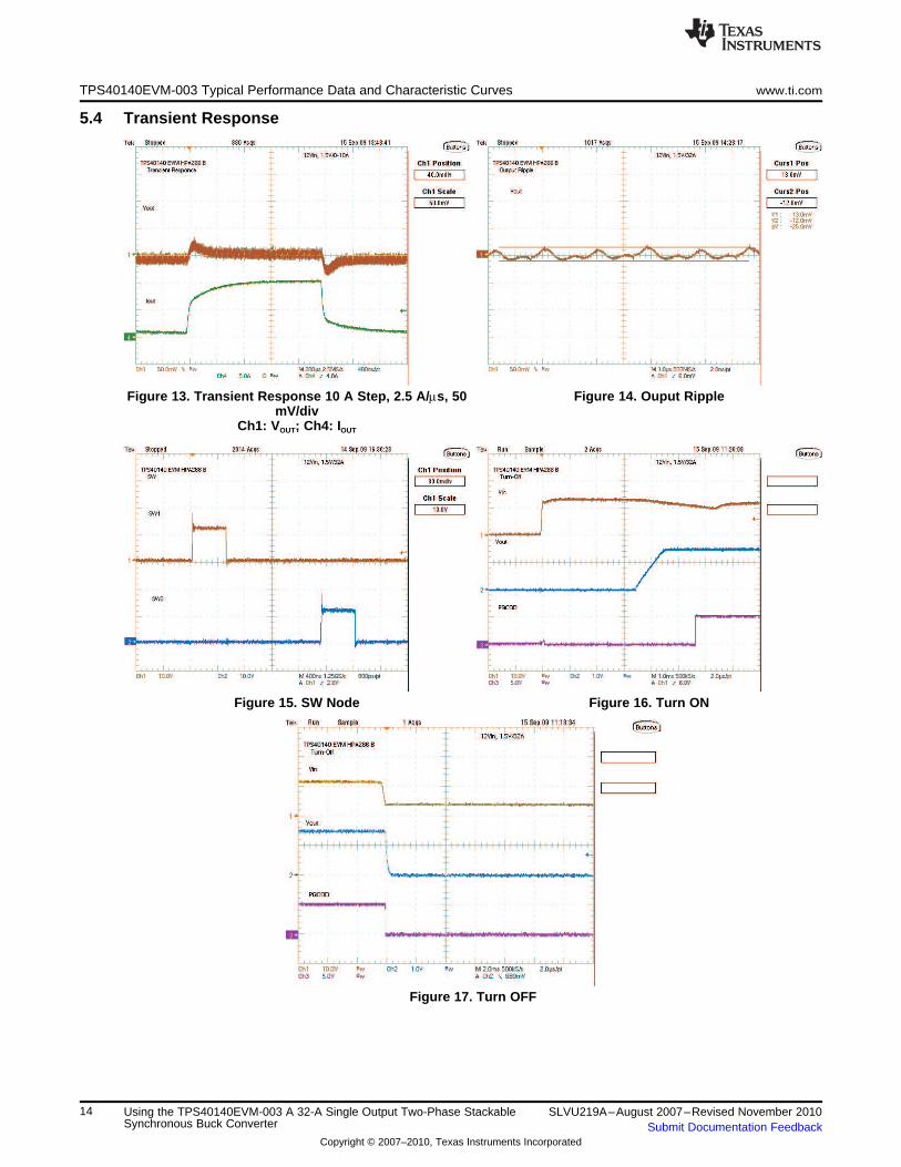
5.4 Transient Response
Figure 13. Transient Response 10 A Step, 2.5 A/ms, 50 Figure 14. Ouput RipplemV/div
Ch1: VOUT; Ch4: IOUT
Figure 15. SW Node Figure 16. Turn ON
Figure 17. Turn OFF
14 Using the TPS40140EVM-003 A 32-A Single Output Two-Phase Stackable SLVU219A–August 2007–Revised November 2010Synchronous Buck Converter Submit Documentation Feedback
Copyright © 2007–2010, Texas Instruments Incorporated

www.ti.com EVM Assembly Drawings and Layout
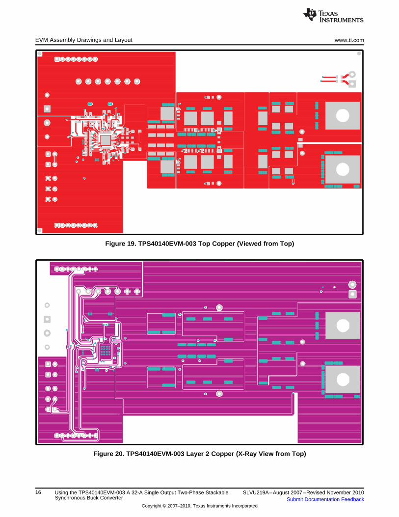
6 EVM Assembly Drawings and Layout
Figure 18 through Figure 22 show the design of the TPS40140EVM-003 printed circuit board. The EVMhas been designed using a four layer, 2 oz copper-clad circuit board with all components on the top sideto allow the user to easily view, probe and evaluate the TPS40140 control IC in a practical application.Moving components to both sides of the PCB or using additional internal layers can offer additional sizereduction for space constrained systems.
Figure 18. TPS40140EVM-003 Component Placement (Viewed from Top)
15SLVU219A–August 2007–Revised November 2010 Using the TPS40140EVM-003 A 32-A Single Output Two-Phase StackableSynchronous Buck ConverterSubmit Documentation Feedback
Copyright © 2007–2010, Texas Instruments Incorporated
EVM Assembly Drawings and Layout www.ti.com
Figure 19. TPS40140EVM-003 Top Copper (Viewed from Top)
Figure 20. TPS40140EVM-003 Layer 2 Copper (X-Ray View from Top)
16 Using the TPS40140EVM-003 A 32-A Single Output Two-Phase Stackable SLVU219A–August 2007–Revised November 2010Synchronous Buck Converter Submit Documentation Feedback
Copyright © 2007–2010, Texas Instruments Incorporated

www.ti.com EVM Assembly Drawings and Layout
Figure 21. TPS40140EVM-003 Layer 3 Copper (X-Ray View from Top)
Figure 22. TPS40140EVM-003 Bottom Copper (X-Ray View from Top)
17SLVU219A–August 2007–Revised November 2010 Using the TPS40140EVM-003 A 32-A Single Output Two-Phase StackableSynchronous Buck ConverterSubmit Documentation Feedback
Copyright © 2007–2010, Texas Instruments Incorporated
List of Materials www.ti.com
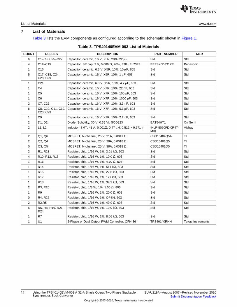
7 List of Materials
Table 3 lists the EVM components as configured according to the schematic shown in Figure 1.
Table 3. TPS40140EVM-003 List of Materials
COUNT REFDES DESCRIPTION PART NUMBER MFR
6 C1–C3, C25–C27 Capacitor, ceramic, 16 V, X5R, 20%, 22 mF Std Std
4 C12–C15 Capacitor, SP cap, 2 V, 0.006 Ω, 20%, 330 mF, 7343 EEFSX0D331XE Panasonic
1 C16 Capacitor, ceramic, 6.3 V, X5R, 10%, 10 mF, 805 Std Std
5 C17, C18, C24, Capacitor, ceramic, 16 V, X5R, 10%, 1 mF, 603 Std StdC28, C29
1 C21 Capacitor, ceramic, 6.3 V, X5R, 10%, 4.7 mF, 603 Std Std
1 C4 Capacitor, ceramic, 16 V, X7R, 10%, 22 nF, 603 Std Std
1 C5 Capacitor, ceramic, 16 V, X7R, 10%, 100 pF, 603 Std Std
1 C6 Capacitor, ceramic, 16 V, X7R, 10%, 1000 pF, 603 Std Std
2 C7, C22 Capacitor, ceramic, 16 V, X7R, 10%, 3.3 nF, 603 Std Std
6 C8, C10, C11, C19, Capacitor, ceramic, 16 V, X7R, 10%, 0.1 mF, 603 Std StdC20, C23
1 C9 Capacitor, ceramic, 16 V, X7R, 10%, 2.2 nF, 603 Std Std
2 D1, D2 Diode, Schottky, 30 V, 0.35 Vf, SOD323 BAT54HT1 On Semi
2 L1, L2 Inductor, SMT, 41 A, 0.001Ω, 0.47 mH, 0.512 × 0.571 in IHLP-5050FD-0R47- VishayM01
2 Q1, Q6 MOSFET, N-channel, 25 V, 21A, 0.0041 Ω CSD16404Q5A TI
2 Q2, Q4 MOSFET, N-channel, 25 V, 38A, 0.0018 Ω CSD16401Q5 TI
0 Q3, Q5 MOSFET, N-channel, 25 V, 38A, 0.0018 Ω CSD16401Q5 TI
2 R1, R23 Resistor, chip, 1/16 W, 1%, 3.01 kΩ, 603 Std Std
4 R10–R12, R18 Resistor, chip, 1/16 W, 1%, 10.0 Ω, 603 Std Std
1 R16 Resistor, chip, 1/16 W, 1%, 4.70 Ω, 603 Std Std
1 R14 Resistor, chip, 1/16 W, 1%, 511 kΩ, 603 Std Std
1 R15 Resistor, chip, 1/16 W, 1%, 22.6 kΩ, 603 Std Std
1 R17 Resistor, chip, 1/16 W, 1%, 127 kΩ, 603 Std Std
1 R13 Resistor, chip, 1/16 W, 1%, 39.2 kΩ, 603 Std Std
2 R3, R20 Resistor, chip, 1/8 W, 1%, 1.00 Ω, 805 Std Std
1 R9 Resistor, chip, 1/16 W, 1%, 20.0 Ω, 603 Std Std
0 R4, R22 Resistor, chip, 1/16 W, 1%, OPEN, 603 Std Std
2 R2,R5 Resistor, chip, 1/16 W, 1%, 49.9 Ω, 603 Std Std
5 R6, R8, R19, R21, Resistor, chip, 1/16 W, 1%, 10.0 kΩ, 603 Std StdR24
1 R7 Resistor, chip, 1/16 W, 1%, 8.66 kΩ, 603 Std Std
1 U1 2-Phase or Dual Output PWM Controller, QFN-36 TPS40140RHH Texas Instruments
18 Using the TPS40140EVM-003 A 32-A Single Output Two-Phase Stackable SLVU219A–August 2007–Revised November 2010Synchronous Buck Converter Submit Documentation Feedback
Copyright © 2007–2010, Texas Instruments Incorporated

EVALUATION BOARD/KIT IMPORTANT NOTICE
Texas Instruments (TI) provides the enclosed product(s) under the following conditions:
This evaluation board/kit is intended for use for ENGINEERING DEVELOPMENT, DEMONSTRATION, OR EVALUATION PURPOSESONLY and is not considered by TI to be a finished end-product fit for general consumer use. Persons handling the product(s) must haveelectronics training and observe good engineering practice standards. As such, the goods being provided are not intended to be completein terms of required design-, marketing-, and/or manufacturing-related protective considerations, including product safety and environmentalmeasures typically found in end products that incorporate such semiconductor components or circuit boards. This evaluation board/kit doesnot fall within the scope of the European Union directives regarding electromagnetic compatibility, restricted substances (RoHS), recycling(WEEE), FCC, CE or UL, and therefore may not meet the technical requirements of these directives or other related directives.
Should this evaluation board/kit not meet the specifications indicated in the User’s Guide, the board/kit may be returned within 30 days fromthe date of delivery for a full refund. THE FOREGOING WARRANTY IS THE EXCLUSIVE WARRANTY MADE BY SELLER TO BUYERAND IS IN LIEU OF ALL OTHER WARRANTIES, EXPRESSED, IMPLIED, OR STATUTORY, INCLUDING ANY WARRANTY OFMERCHANTABILITY OR FITNESS FOR ANY PARTICULAR PURPOSE.
The user assumes all responsibility and liability for proper and safe handling of the goods. Further, the user indemnifies TI from all claimsarising from the handling or use of the goods. Due to the open construction of the product, it is the user’s responsibility to take any and allappropriate precautions with regard to electrostatic discharge.
EXCEPT TO THE EXTENT OF THE INDEMNITY SET FORTH ABOVE, NEITHER PARTY SHALL BE LIABLE TO THE OTHER FOR ANYINDIRECT, SPECIAL, INCIDENTAL, OR CONSEQUENTIAL DAMAGES.
TI currently deals with a variety of customers for products, and therefore our arrangement with the user is not exclusive.
TI assumes no liability for applications assistance, customer product design, software performance, or infringement of patents orservices described herein.
Please read the User’s Guide and, specifically, the Warnings and Restrictions notice in the User’s Guide prior to handling the product. Thisnotice contains important safety information about temperatures and voltages. For additional information on TI’s environmental and/orsafety programs, please contact the TI application engineer or visit www.ti.com/esh.
No license is granted under any patent right or other intellectual property right of TI covering or relating to any machine, process, orcombination in which such TI products or services might be or are used.
FCC Warning
This evaluation board/kit is intended for use for ENGINEERING DEVELOPMENT, DEMONSTRATION, OR EVALUATION PURPOSESONLY and is not considered by TI to be a finished end-product fit for general consumer use. It generates, uses, and can radiate radiofrequency energy and has not been tested for compliance with the limits of computing devices pursuant to part 15 of FCC rules, which aredesigned to provide reasonable protection against radio frequency interference. Operation of this equipment in other environments maycause interference with radio communications, in which case the user at his own expense will be required to take whatever measures maybe required to correct this interference.
EVM WARNINGS AND RESTRICTIONS
It is important to operate this EVM within the input voltage range of 10.8 V to 13.2 V and the output voltage range of 1.5 V at 0–32 A.
Exceeding the specified input range may cause unexpected operation and/or irreversible damage to the EVM. If there are questionsconcerning the input range, please contact a TI field representative prior to connecting the input power.
Applying loads outside of the specified output range may result in unintended operation and/or possible permanent damage to the EVM.Please consult the EVM User's Guide prior to connecting any load to the EVM output. If there is uncertainty as to the load specification,please contact a TI field representative.
During normal operation, some circuit components may have case temperatures greater than 85 °C. The EVM is designed to operateproperly with certain components above 85 °C as long as the input and output ranges are maintained. These components include but arenot limited to linear regulators, switching transistors, pass transistors, and current sense resistors. These types of devices can be identifiedusing the EVM schematic located in the EVM User's Guide. When placing measurement probes near these devices during operation,please be aware that these devices may be very warm to the touch.
Mailing Address: Texas Instruments, Post Office Box 655303, Dallas, Texas 75265Copyright © 2007, Texas Instruments Incorporated
IMPORTANT NOTICE
Texas Instruments Incorporated and its subsidiaries (TI) reserve the right to make corrections, modifications, enhancements, improvements,and other changes to its products and services at any time and to discontinue any product or service without notice. Customers shouldobtain the latest relevant information before placing orders and should verify that such information is current and complete. All products aresold subject to TI’s terms and conditions of sale supplied at the time of order acknowledgment.
TI warrants performance of its hardware products to the specifications applicable at the time of sale in accordance with TI’s standardwarranty. Testing and other quality control techniques are used to the extent TI deems necessary to support this warranty. Except wheremandated by government requirements, testing of all parameters of each product is not necessarily performed.
TI assumes no liability for applications assistance or customer product design. Customers are responsible for their products andapplications using TI components. To minimize the risks associated with customer products and applications, customers should provideadequate design and operating safeguards.
TI does not warrant or represent that any license, either express or implied, is granted under any TI patent right, copyright, mask work right,or other TI intellectual property right relating to any combination, machine, or process in which TI products or services are used. Informationpublished by TI regarding third-party products or services does not constitute a license from TI to use such products or services or awarranty or endorsement thereof. Use of such information may require a license from a third party under the patents or other intellectualproperty of the third party, or a license from TI under the patents or other intellectual property of TI.
Reproduction of TI information in TI data books or data sheets is permissible only if reproduction is without alteration and is accompaniedby all associated warranties, conditions, limitations, and notices. Reproduction of this information with alteration is an unfair and deceptivebusiness practice. TI is not responsible or liable for such altered documentation. Information of third parties may be subject to additionalrestrictions.
Resale of TI products or services with statements different from or beyond the parameters stated by TI for that product or service voids allexpress and any implied warranties for the associated TI product or service and is an unfair and deceptive business practice. TI is notresponsible or liable for any such statements.
TI products are not authorized for use in safety-critical applications (such as life support) where a failure of the TI product would reasonablybe expected to cause severe personal injury or death, unless officers of the parties have executed an agreement specifically governingsuch use. Buyers represent that they have all necessary expertise in the safety and regulatory ramifications of their applications, andacknowledge and agree that they are solely responsible for all legal, regulatory and safety-related requirements concerning their productsand any use of TI products in such safety-critical applications, notwithstanding any applications-related information or support that may beprovided by TI. Further, Buyers must fully indemnify TI and its representatives against any damages arising out of the use of TI products insuch safety-critical applications.
TI products are neither designed nor intended for use in military/aerospace applications or environments unless the TI products arespecifically designated by TI as military-grade or "enhanced plastic." Only products designated by TI as military-grade meet militaryspecifications. Buyers acknowledge and agree that any such use of TI products which TI has not designated as military-grade is solely atthe Buyer's risk, and that they are solely responsible for compliance with all legal and regulatory requirements in connection with such use.
TI products are neither designed nor intended for use in automotive applications or environments unless the specific TI products aredesignated by TI as compliant with ISO/TS 16949 requirements. Buyers acknowledge and agree that, if they use any non-designatedproducts in automotive applications, TI will not be responsible for any failure to meet such requirements.
Following are URLs where you can obtain information on other Texas Instruments products and application solutions:
Products Applications
Amplifiers amplifier.ti.com Audio www.ti.com/audio
Data Converters dataconverter.ti.com Automotive www.ti.com/automotive
DLP® Products www.dlp.com Communications and www.ti.com/communicationsTelecom
DSP dsp.ti.com Computers and www.ti.com/computersPeripherals
Clocks and Timers www.ti.com/clocks Consumer Electronics www.ti.com/consumer-apps
Interface interface.ti.com Energy www.ti.com/energy
Logic logic.ti.com Industrial www.ti.com/industrial
Power Mgmt power.ti.com Medical www.ti.com/medical
Microcontrollers microcontroller.ti.com Security www.ti.com/security
RFID www.ti-rfid.com Space, Avionics & www.ti.com/space-avionics-defenseDefense
RF/IF and ZigBee® Solutions www.ti.com/lprf Video and Imaging www.ti.com/video
Wireless www.ti.com/wireless-apps
Mailing Address: Texas Instruments, Post Office Box 655303, Dallas, Texas 75265Copyright © 2010, Texas Instruments Incorporated