Embed Size (px)
Citation preview

SCLVPWR
SENn
GATn
DRAINn
DGND
INT
TPS2388SDAO
SDAI
AGND
KSENSx
VDD
+48 V
+3.3 V
PORT100 nF100 V
Note: Only port n shown
255 mO
Product
Folder
Order
Now
Technical
Documents
Tools &
Software
Support &Community
An IMPORTANT NOTICE at the end of this data sheet addresses availability, warranty, changes, use in safety-critical applications,intellectual property matters and other important disclaimers. PRODUCTION DATA.
TPS2388SLUSC25A –FEBRUARY 2015–REVISED AUGUST 2017
TPS2388 IEEE 802.3at 8-Channel Power-over-Ethernet PSE Controller
1
1 Features1• Fully IEEE 802.3at Compliant• Port Re-Mapping• 1- and 3-Bit Fast Port Shutdown Input• “Never Fooled” 4-Point Detection• Type 1 and Type 2 PD Classification• Programmable Current Limit With Foldback• DC Disconnect Detection• Flexible Processor Controlled Operating Modes
– Semiauto– Manual
• 14-Bit Port Current and Voltage Monitoring– 100-ms Rolling Port Current Averaging– 2% Current Sensing Accuracy– 0.255-Ω Sense Resistor With Kelvin Sense
• I2C Communication– I2C Watchdog for Failsafe Operation– 8- and 16-Bit Access Mode Selectable
• –40°C to 125°C Temperature Operation• 56-Lead VQFN Package
2 Applications• Enterprise Switches and Routers• SoHo Switches and Routers• PoE Pass-Through Power Modules• Network Video Recorders (NVRs)
3 DescriptionThe TPS2388 is an 8-channel power sourceequipment (PSE) controller engineered to insertpower onto Ethernet cable according to IEEE802.3at-2012 standard (or 802.3at). The PSEcontroller can detect powered devices (PDs) thathave a valid signature, determine the powerrequirements according to the classification, andapply power through either one (Type -1) or two-event (Type-2) physical classification. The TPS2388also has the flexibility to support UPoE and othernon-standard loads.
The Port remapping and the device pinout allowdesigners to enable 2-layer PCB designs and simplifysoftware migration from previous generation PSEdevices. The external FET architecture allowsdesigners to further balance size, efficiency, thermal,and solution cost requirements. The current foldbackreduces thermal stress on the external MOSFETsduring startup and overload conditions allowing theuse of cheaper FETs.
The Fast Shutdown (OSS) input provides up to eightlevels of per port shutdown priority for applicationsthat require the immediate disabling of multiple ports.
Device Information(1)
PART NUMBER PACKAGE BODY SIZE (NOM)TPS2388 VQFN (56) 8.00 mm × 8.00 mm
(1) For all available packages, see the orderable addendum atthe end of the data sheet.
Simplified Schematic

2
TPS2388SLUSC25A –FEBRUARY 2015–REVISED AUGUST 2017 www.ti.com
Product Folder Links: TPS2388
Submit Documentation Feedback Copyright © 2015–2017, Texas Instruments Incorporated
Table of Contents1 Features .................................................................. 12 Applications ........................................................... 13 Description ............................................................. 14 Revision History..................................................... 25 Pin Configuration and Functions ......................... 3
5.1 Detailed Pin Description............................................ 46 Specifications......................................................... 6
6.1 Absolute Maximum Ratings ...................................... 66.2 ESD Ratings ............................................................ 66.3 Recommended Operating Conditions....................... 66.4 Thermal Information .................................................. 76.5 Electrical Characteristics........................................... 76.6 Timing Requirements ............................................. 106.7 Switching Characteristics ........................................ 116.8 Typical Characteristics ............................................ 12
7 Parameter Measurement Information ................ 147.1 Timing Diagrams..................................................... 14
8 Detailed Description ............................................ 168.1 Overview ................................................................. 168.2 Functional Block Diagram ....................................... 17
8.3 Feature Description................................................. 188.4 Device Functional Modes........................................ 208.5 Programming .......................................................... 218.6 Register Maps ......................................................... 24
9 Application and Implementation ........................ 649.1 Application Information............................................ 649.2 Typical Application ................................................. 66
10 Power Supply Recommendations ..................... 7210.1 VDD....................................................................... 7210.2 VPWR ................................................................... 72
11 Layout................................................................... 7211.1 Layout Guidelines ................................................. 7211.2 Layout Example .................................................... 73
12 Device and Documentation Support ................. 7412.1 Receiving Notification of Documentation Updates 7412.2 Community Resources.......................................... 7412.3 Trademarks ........................................................... 7412.4 Electrostatic Discharge Caution............................ 7412.5 Glossary ................................................................ 74
13 Mechanical, Packaging, and OrderableInformation ........................................................... 74
4 Revision History
DATE REVISION NOTESAugust 2017 * 1st public release of data sheet.

89
1011121314
DRAIN3
DRAIN4
GAT4SEN4
15 16 17 18 19 20 21
NC
NC
SEN3
OS
SS
DA
O56 55 54 53 52 51 50
NC
NC
AT
ST
_DC
PL0
AG
ND
Res
vS
CL
A4
A3
SD
AI
35343332313029
VP
WR
22 23 24
NC
TE
ST
1T
ES
T2
1234567
DRAIN1KSENSADRAIN2
GAT2SEN2
SEN1
25T
ES
T3
26 27 28
TE
ST
0
Res
vR
esv
42414039383736
A2
A1
49 48 47 46 45 44 43
INT
DG
ND
RE
SE
TV
DD
DT
ST
_DC
PL1
GAT1
GAT3
KSENSBDRAIN6
DRAIN5
GAT5SEN5
SEN6
DRAIN8KSENSDDRAIN7
GAT7SEN7
SEN8
GAT8
GAT6
KSENSC
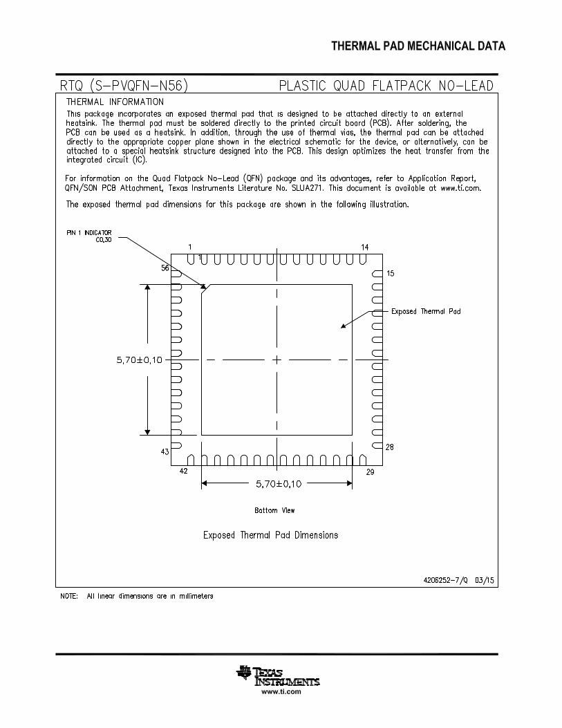
Thermal Pad
3
TPS2388www.ti.com SLUSC25A –FEBRUARY 2015–REVISED AUGUST 2017
Product Folder Links: TPS2388
Submit Documentation FeedbackCopyright © 2015–2017, Texas Instruments Incorporated
5 Pin Configuration and Functions
RTQ PackageVQFN 56 Pins
Top View
Pin FunctionsPIN
I/O DESCRIPTIONNAME NO.
A1-4 48–51 I I2C A1-A4 address lines. These pins are internally pulled up to VDD.
AGND 21 — Analog ground. Connect to GND plane and exposed thermal pad.
ATST_DCPL0 20 O Used for internal test purposes, no bypass capacitor is needed.
DGND 46 — Digital ground. Connect to GND plane and exposed thermal pad.
DRAIN1-8 3, 5, 10, 12, 31,33, 38, 40 I Port 1-8 output voltage monitor.
DTST_DCPL1 47 O Used for internal test purposes, no bypass capacitor is needed.
GAT1-8 1, 7, 8, 14, 29,35, 36, 42 O Port 1-8 gate drive output.
INT 45 O Interrupt output. This pin asserts low when a bit in the interrupt register is asserted. This output is open-drain.
KSENSA/B 4, 11 I Kelvin point connection for SEN1-4
KSENSC/D 32, 39 I Kelvin point connection for SEN5-8

4
TPS2388SLUSC25A –FEBRUARY 2015–REVISED AUGUST 2017 www.ti.com
Product Folder Links: TPS2388
Submit Documentation Feedback Copyright © 2015–2017, Texas Instruments Incorporated
Pin Functions (continued)PIN
I/O DESCRIPTIONNAME NO.
NC15, 16, 18, 19 O No connect pins. These pins are internally biased at 1/3 and 2/3 of VPWR in order to control the voltage
gradient from VPWR. Leave open.
22 — No connect pin. Leave open.
OSS 56 I Port 1-8 fast shutdown. This pin is internally pulled down to DGND.
Thermal pad — — The DGND and AGND terminals must be connected to the exposed thermal pad for proper operation.
RESET 44 I Reset input. When asserted low, the TPS2388 is reset. This pin is internally pulled up to VDD.
Resv 27, 28, 52 — Reserved. No connect pins. Leave open.
SCL 53 I Serial clock input for I2C bus.
SDAI 54 I Serial data input for I2C bus. This pin can be connected to SDAO for non-isolated systems.
SDAO 55 O Serial data output for I2C bus. This pin can be connected to SDAI for non-isolated systems. This output is open-drain.
SEN1-8 2, 6, 9, 13, 30,34, 37, 41 I Port 1-8 current sense input.
TEST0-3 23, 24, 25, 26 I/O Used internally for test purposes only. Leave open.
VDD 43 — Digital supply. Bypass with 0.1 µF to DGND pin.
VPWR 17 — Analog 48-V positive supply. Bypass with 0.1 µF to AGND pin.
5.1 Detailed Pin DescriptionThe following descriptions refer to the pinout and the functional block diagram.
DRAIN1-DRAIN8: Port 1-8 output voltage monitor and detect sense. Used to measure the port output voltage,for port voltage monitoring, port power good detection and foldback action. Detection probe currents also flowinto this pin.
The TPS2388 uses an innovative 4-point technique to provide reliable PD detection. The discovery is performedby sinking two different current levels via the DRAINn pin, while the PD voltage is measured from VPWR toDRAINn. The 4-point measurement provides the capability to avoid powering a capacitive or legacy load. Also,while in semiauto mode, if prior to starting a new detection cycle the port voltage is >2.5 V, an internal 100-kΩresistor is connected in parallel with the port and a 400-ms detect backoff period is applied to allow the portcapacitor to be discharged before the detection cycle starts.
There is an internal resistor between each DRAINn pin and VPWR in any operating mode except duringdetection or while the port is ON. If the port n is not used, DRAINn can be left floating or tied to AGND.
GAT1-GAT8: Port 1-8 gate drive output is used for external N-channel MOSFET gate control. At port turn on, itis driven positive by a low current source to turn the MOSFET on. GATn is pulled low whenever any of the inputsupplies are low or if an overcurrent timeout has occurred. GATn is also pulled low if its port is turned off by useof manual shutdown inputs. Leave floating if unused.
For a robust design, a current foldback function limits the power dissipation of the MOSFET during low resistanceload or a short-circuit event. During inrush, the foldback mechanism measures the port voltage across VPWRand DRAINn to reduce the current limit threshold as shown in Figure 17.
When ICUT threshold is exceeded while a port is on, a timer starts. During that time, linear current limiting ensuresthe current does not exceed ILIM combined with current foldback action. When the timer reaches its tOVLD (ortSTART if at port turn on) limit, the part shuts off. When the port current goes below ICUT, the counter counts downat a rate 1/16th of the increment rate and it must reach a count of 0 before the port can be turned on again.
The fast overload protection is for major faults like a direct short. This forces the MOSFET into current limit inless than a microsecond.
The circuit leakage paths between the GATn pin and any nearby DRAINn pin, GND or Kelvin point connectionmust be minimized (<250 nA), to ensure correct MOSFET control.
INT: This interrupt output pin asserts low when a bit in the interrupt register is asserted. This output is open-drain.
KSENSA, KSENSB, KSENSC, KSENSD: Kelvin point connection used to perform a differential voltagemeasurement across the associated current sense resistors.

5
TPS2388www.ti.com SLUSC25A –FEBRUARY 2015–REVISED AUGUST 2017
Product Folder Links: TPS2388
Submit Documentation FeedbackCopyright © 2015–2017, Texas Instruments Incorporated
Detailed Pin Description (continued)Each KSENS is shared between two neighbor SEN pins as following: KSENSA with SEN1 and SEN2, KSENSBwith SEN3 and SEN4, KSENSC with SEN5 and SEN6, KSENSD with SEN7 and SEN8. To optimize theaccuracy of the measurement, take care with the PCB layout to minimize the impact of the PCB traces'resistance.
OSS: Fast shutdown, active high. This pin is internally pulled down to DGND, with an internal 1-µs to 5-µsdeglitch filter.
The Port Power Priority/ICUT Disable register is used to determine which port is shut down in response to anexternal assertion of the OSS fast shutdown signal. The turn off procedure is similar to a port reset using Resetcommand (1Ah register).
RESET: Reset input, active low. When asserted, the TPS2388 resets, turning off all ports and forcing theregisters to their power-up state. This pin is internally pulled up to VDD, with internal 1-µs to 5-µs deglitch filter.The designer can use an external RC network to delay the turn-on. There is also an internal power-on-resetwhich is independent of the RESET input.
NOTEDuring the first 5 ms after RESET has been asserted, if a port is turned on using thePower Enable command (0x19), TI recommends to wait for the expiration of that 5-msinitial period before sending any subsequent Detect/Class Restart or Detect/Class Enablecommand.
SCL: Serial clock input for I2C bus.
SDAI: Serial data input for I2C bus. This pin can be connected to SDAO for non-isolated systems.
SDAO: Open-drain I2C bus output data line. Requires an external resistive pull-up. The TPS2388 uses separateSDAO and SDAI lines to allow optoisolated I2C interface. SDAO can be connected to SDAI for non-isolatedsystems.
A4-A1: I2C bus address inputs. These pins are internally pulled up to VDD. See Pin Status Register for moredetails.
SEN1-8: Port current sense input relative to KSENSn (see KSENSn description). A differential measurement isperformed using KSENSA-D Kelvin point connection. Monitors the external MOSFET current by use of a 0.255-Ωcurrent sense resistor connected to DGND. Used by current foldback engine and also during classification. Canbe used to perform load current monitoring via A/D conversion.
Note that a classification is done while using the external MOSFET so that doing a classification on more thanone port at same time is possible without overdissipation in the TPS2388. For the current limit with foldbackfunction, there is an internal 2-µS analog filter on the SEN1-8 pins to provide glitch filtering. For measurementsthrough an A/D converter, an anti-aliasing filter is present on the SEN1-8 pins. This includes the port-poweredcurrent monitoring, port policing, and DC disconnect.
If the port is not used, tie SENn to AGND.
VDD: 3.3-V logic power supply input.
VPWR: High voltage power supply input. Nominally 48 V.
6
TPS2388SLUSC25A –FEBRUARY 2015–REVISED AUGUST 2017 www.ti.com
Product Folder Links: TPS2388
Submit Documentation Feedback Copyright © 2015–2017, Texas Instruments Incorporated
(1) Stresses beyond those listed under Absolute Maximum Ratings may cause permanent damage to the device. These are stress ratingsonly, which do not imply functional operation of the device at these or any other conditions beyond those indicated under RecommendedOperating Conditions. Exposure to absolute-maximum-rated conditions for extended periods may affect device reliability.
(2) SEN1-8 are tolerant to 15-V transients to avoid fault propagation when a MOSFET fails in short-circuit(3) Application of voltage is not implied; these are internally driven pins.(4) If the external MOSFET fails short between its drain and gate, the GATE pin may internally permanently disconnect to prevent cascade
damage. The three other ports continue to operate.(5) Do not apply external voltage sources directly(6) Short transients (µs range) up to 80 V are allowed
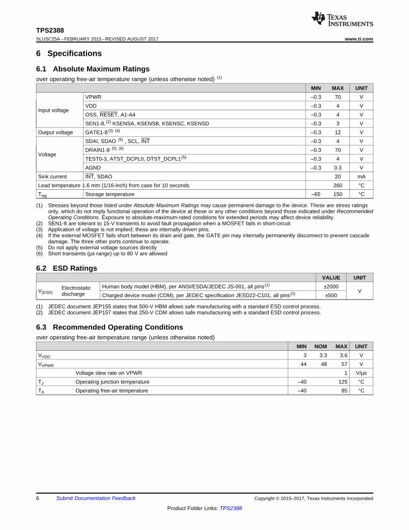
6 Specifications
6.1 Absolute Maximum Ratingsover operating free-air temperature range (unless otherwise noted) (1)
MIN MAX UNIT
Input voltage
VPWR –0.3 70 VVDD –0.3 4 VOSS, RESET, A1-A4 –0.3 4 VSEN1-8, (2) KSENSA, KSENSB, KSENSC, KSENSD –0.3 3 V
Output voltage GATE1-8 (3) (4) –0.3 12 V
Voltage
SDAI, SDAO (5) , SCL, INT –0.3 4 VDRAIN1-8 (5) (6) –0.3 70 VTEST0-3, ATST_DCPL0, DTST_DCPL1 (5) –0.3 4 VAGND –0.3 0.3 V
Sink current INT, SDAO 20 mALead temperature 1.6 mm (1/16-inch) from case for 10 seconds 260 °CTstg Storage temperature –65 150 °C
(1) JEDEC document JEP155 states that 500-V HBM allows safe manufacturing with a standard ESD control process.(2) JEDEC document JEP157 states that 250-V CDM allows safe manufacturing with a standard ESD control process.
6.2 ESD RatingsVALUE UNIT
V(ESD)Electrostaticdischarge
Human body model (HBM), per ANSI/ESDA/JEDEC JS-001, all pins (1) ±2000V
Charged device model (CDM), per JEDEC specification JESD22-C101, all pins (2) ±500
6.3 Recommended Operating Conditionsover operating free-air temperature range (unless otherwise noted)
MIN NOM MAX UNITVVDD 3 3.3 3.6 VVVPWR 44 48 57 V
Voltage slew rate on VPWR 1 V/µsTJ Operating junction temperature –40 125 °CTA Operating free-air temperature –40 85 °C

7
TPS2388www.ti.com SLUSC25A –FEBRUARY 2015–REVISED AUGUST 2017
Product Folder Links: TPS2388
Submit Documentation FeedbackCopyright © 2015–2017, Texas Instruments Incorporated
(1) For more information about traditional and new thermal metrics, see the IC Package Thermal Metrics application report, SPRA953.
6.4 Thermal Information
THERMAL METRIC (1) TPS2388UNIT
VQFN (56 PINS)RθJA Junction-to-ambient thermal resistance 25.3
°C/W
RθJC(top) Junction-to-case (top) thermal resistance 9.7RθJB Junction-to-board thermal resistance 3.7ψJT Junction-to-top characterization parameter 0.2ψJB Junction-to-board characterization parameter 3.7RθJC(bot) Junction-to-case (bottom) thermal resistance 0.5
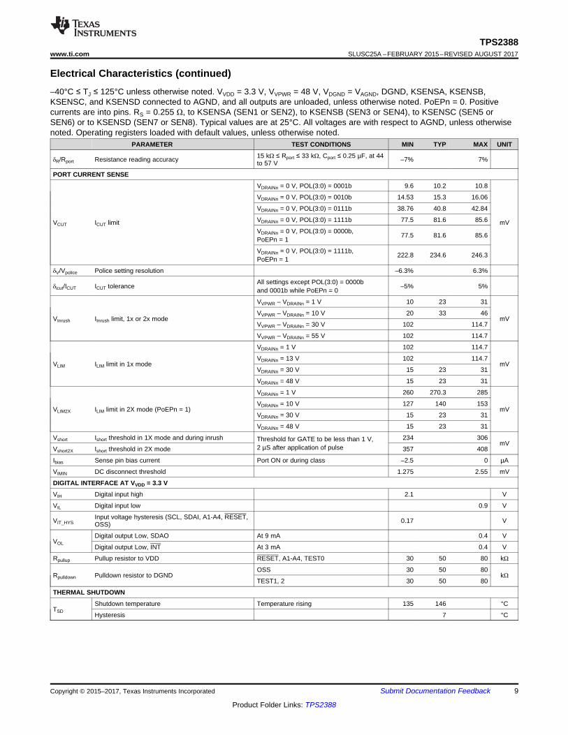
6.5 Electrical Characteristics–40°C ≤ TJ ≤ 125°C unless otherwise noted. VVDD = 3.3 V, VVPWR = 48 V, VDGND = VAGND, DGND, KSENSA, KSENSB,KSENSC, and KSENSD connected to AGND, and all outputs are unloaded, unless otherwise noted. PoEPn = 0. Positivecurrents are into pins. RS = 0.255 Ω, to KSENSA (SEN1 or SEN2), to KSENSB (SEN3 or SEN4), to KSENSC (SEN5 orSEN6) or to KSENSD (SEN7 or SEN8). Typical values are at 25°C. All voltages are with respect to AGND, unless otherwisenoted. Operating registers loaded with default values, unless otherwise noted.
PARAMETER TEST CONDITIONS MIN TYP MAX UNIT
INPUT SUPPLY VPWR
IVPWR VPWR current consumptionVVPWR = 50 V 10 12.5 mA
VVPWR < 8 V 100 µA
VUVLOPW_F VPWR UVLO falling threshold 14.5 17.5 V
VUVLOPW_R VPWR UVLO rising threshold 15.5 18.5 V
VPUV_F VPWR undervoltage falling threshold VPUV threshold 25 26.5 28 V
TOTAL DEVICE POWER DISSIPATION
PT VPWR and VDD consumption VVPWR = 50 V 0.67 W
INPUT SUPPLY VDD
IVDD VDD Current consumption 6 12 mA
VUVDD_F VDD UVLO falling threshold For port deassertion 2.1 2.25 2.4 V
VUVDD_R VDD UVLO rising threshold 2.45 2.6 2.75 V
VUVDD_HYS Hysteresis VDD UVLO 0.35 V
VUVW_F VDD UVLO warning threshold 2.6 2.8 3.0 V
DETECTION
IDISC Detection current
First detection point, VVPWR – VDRAINn = 0 V 145 160 190
µASecond detection point, VVPWR – VDRAINn = 0V 235 270 300
High-current detection point, VVPWR –VDRAINn = 0 V 490 540 585
Vdetect Open-circuit detection voltage VVPWR – VDRAINn 23.5 26 29 V
RREJ_LOW Rejected resistance low range 0.86 15 kΩ
RREJ_HI Rejected resistance high range 33 100 kΩ
RACCEPT Accepted resistance range 19 25 26.5 kΩ
RSHORT Shorted port threshold 360 Ω
ROPEN Open port threshold 400 kΩ

8
TPS2388SLUSC25A –FEBRUARY 2015–REVISED AUGUST 2017 www.ti.com
Product Folder Links: TPS2388
Submit Documentation Feedback Copyright © 2015–2017, Texas Instruments Incorporated
Electrical Characteristics (continued)–40°C ≤ TJ ≤ 125°C unless otherwise noted. VVDD = 3.3 V, VVPWR = 48 V, VDGND = VAGND, DGND, KSENSA, KSENSB,KSENSC, and KSENSD connected to AGND, and all outputs are unloaded, unless otherwise noted. PoEPn = 0. Positivecurrents are into pins. RS = 0.255 Ω, to KSENSA (SEN1 or SEN2), to KSENSB (SEN3 or SEN4), to KSENSC (SEN5 orSEN6) or to KSENSD (SEN7 or SEN8). Typical values are at 25°C. All voltages are with respect to AGND, unless otherwisenoted. Operating registers loaded with default values, unless otherwise noted.
PARAMETER TEST CONDITIONS MIN TYP MAX UNIT
CLASSIFICATION
VCLASS Classification voltage VVPWR – VDRAINn, VSENn ≥ 0 mV,Iport ≥ 180 µA 15.5 18.5 20.5 V
ICLASS_Lim Classification current limit VVPWR – VDRAINn = 0 V 65 75 90 mA
ICLASS_TH Classification threshold current
Class 0-1 5 8 mA
Class 1-2 13 16 mA
Class 2-3 21 25 mA
Class 3-4 31 35 mA
Class 4-Class overcurrent 45 51 mA
VMARK Mark voltage 4 mA ≥ Iport ≥ 180 µA, VVPWR – VDRAINn 7 10 V
IMARK_Lim Mark sinking current limit VVPWR – VDRAINn = 0 V 10 70 90 mA
GATE
VGOH Gate drive voltage VGATEn , IGATE = –1 µA 10 12.5 V
IGO-Gate sinking current with Power-on Reset, OSSdetected or port turn off command VGATEn = 5 V 60 100 190 mA
IGO short– Gate sinking current with port short-circuit VGATEn = 5 V, VSENn ≥ Vshort (or Vshort2X if2X mode) 60 100 190 mA
IGO+ Gate sourcing current VGATEn = 0V 39 50 63 µA
DRAIN INPUT
VPGT Power Good threshold Measured at VDRAINn 1.0 2.13 3 V
VSHT Shorted FET threshold Measured at VDRAINn 4 6 8 V
RDRAIN Resistance from DRAINn to VPWRAny operating mode except during detectionor while the port is ON, including in deviceRESET state
80 100 190 kΩ
IDRAIN DRAINn pin bias current VVPWR – VDRAINn = 30 V, port ON 75 120 µA
A/D CONVERTER
tCONV Conversion time, current measurement All ranges, each port 0.64 0.8 0.96 ms
tCONV_V Conversion time, voltage measurement All ranges, each port 0.82 1.03 1.2 ms
tGAP
Gap between adjacent current measurementintegrations 5% × tCONV ms
Gap between adjacent current averaged results 5% ×tINT_CUR
ms
ADCBW ADC integration bandwidth (–3 db) Current measurement 320 Hz
tINT_CUR Integration (averaging) time, current Each port, port ON current 82 102 122 ms
tINT_DET Integration (averaging) time, detection 13.1 16.6 20 ms
tINT_portV Integration (averaging) time, port voltage Port powered 3.25 4.12 4.9 ms
tINT_inV Integration (averaging) time, input voltage 3.25 4.12 4.9 ms
Powered port voltage conversion scale factor andaccuracy
At VVPWR – VDRAINn = 57 V 15097 15565 16032 Counts
At VVPWR – VDRAINn = 44 V 11654 12015 12375 Counts
Powered port current conversion scale factor andaccuracy
At port current = 770 mA 12363 12616 12868 Counts
At port current = 7.5 mA 100 123 150 Counts
Input voltage conversion scale factor and accuracyAt VVPWR = 57 V 15175 15565 15955 Counts
At VVPWR = 44 V 11713 12015 12316 Counts
δV/Vport Voltage reading accuracy At 44 to 57 V –3% 3%
σV Voltage reading repeatability Full scale reading –18 18 mV
δI/Iport Current reading accuracyAt 50 mA –3% 3%
At 770 mA -2% 2%
σI Current reading repeatability Full scale reading –7.5 7.5 mA
9
TPS2388www.ti.com SLUSC25A –FEBRUARY 2015–REVISED AUGUST 2017
Product Folder Links: TPS2388
Submit Documentation FeedbackCopyright © 2015–2017, Texas Instruments Incorporated
Electrical Characteristics (continued)–40°C ≤ TJ ≤ 125°C unless otherwise noted. VVDD = 3.3 V, VVPWR = 48 V, VDGND = VAGND, DGND, KSENSA, KSENSB,KSENSC, and KSENSD connected to AGND, and all outputs are unloaded, unless otherwise noted. PoEPn = 0. Positivecurrents are into pins. RS = 0.255 Ω, to KSENSA (SEN1 or SEN2), to KSENSB (SEN3 or SEN4), to KSENSC (SEN5 orSEN6) or to KSENSD (SEN7 or SEN8). Typical values are at 25°C. All voltages are with respect to AGND, unless otherwisenoted. Operating registers loaded with default values, unless otherwise noted.
PARAMETER TEST CONDITIONS MIN TYP MAX UNIT
δR/Rport Resistance reading accuracy 15 kΩ ≤ Rport ≤ 33 kΩ, Cport ≤ 0.25 µF, at 44to 57 V –7% 7%
PORT CURRENT SENSE
VCUT ICUT limit
VDRAINn = 0 V, POL(3:0) = 0001b 9.6 10.2 10.8
mV
VDRAINn = 0 V, POL(3:0) = 0010b 14.53 15.3 16.06
VDRAINn = 0 V, POL(3:0) = 0111b 38.76 40.8 42.84
VDRAINn = 0 V, POL(3:0) = 1111b 77.5 81.6 85.6
VDRAINn = 0 V, POL(3:0) = 0000b,PoEPn = 1 77.5 81.6 85.6
VDRAINn = 0 V, POL(3:0) = 1111b,PoEPn = 1 222.8 234.6 246.3
δV/Vpolice Police setting resolution –6.3% 6.3%
δicut/ICUT ICUT tolerance All settings except POL(3:0) = 0000band 0001b while PoEPn = 0 –5% 5%
VInrush IInrush limit, 1x or 2x mode
VVPWR – VDRAINn = 1 V 10 23 31
mVVVPWR – VDRAINn = 10 V 20 33 46
VVPWR – VDRAINn = 30 V 102 114.7
VVPWR – VDRAINn = 55 V 102 114.7
VLIM ILIM limit in 1x mode
VDRAINn = 1 V 102 114.7
mVVDRAINn = 13 V 102 114.7
VDRAINn = 30 V 15 23 31
VDRAINn = 48 V 15 23 31
VLIM2X ILIM limit in 2X mode (PoEPn = 1)
VDRAINn = 1 V 260 270.3 285
mVVDRAINn = 10 V 127 140 153
VDRAINn = 30 V 15 23 31
VDRAINn = 48 V 15 23 31
Vshort Ishort threshold in 1X mode and during inrush Threshold for GATE to be less than 1 V,2 µS after application of pulse
234 306mV
Vshort2X Ishort threshold in 2X mode 357 408
Ibias Sense pin bias current Port ON or during class –2.5 0 µA
VIMIN DC disconnect threshold 1.275 2.55 mV
DIGITAL INTERFACE AT VVDD = 3.3 V
VIH Digital input high 2.1 V
VIL Digital input low 0.9 V
VIT_HYSInput voltage hysteresis (SCL, SDAI, A1-A4, RESET,OSS) 0.17 V
VOLDigital output Low, SDAO At 9 mA 0.4 V
Digital output Low, INT At 3 mA 0.4 V
Rpullup Pullup resistor to VDD RESET, A1-A4, TEST0 30 50 80 kΩ
Rpulldown Pulldown resistor to DGNDOSS 30 50 80
kΩTEST1, 2 30 50 80
THERMAL SHUTDOWN
TSDShutdown temperature Temperature rising 135 146 °C
Hysteresis 7 °C

10
TPS2388SLUSC25A –FEBRUARY 2015–REVISED AUGUST 2017 www.ti.com
Product Folder Links: TPS2388
Submit Documentation Feedback Copyright © 2015–2017, Texas Instruments Incorporated
6.6 Timing RequirementsMIN TYP MAX UNIT
fSCL SCL clock frequency 10 400 kHztLOW LOW period of the clock 1.3 µstHIGH HIGH period of the clock 0.6 µs
tfo SDAO output fall time
SDAO, 2.3 → 0.8 V, Cb = 10 pF,10 kΩ pull-up to 3.3 V 21 250 ns
SDAO, 2.3 → 0.8 V, Cb = 400 pF,1.3 kΩ pull-up to 3.3 V 21 250 ns
CI2C SCL capacitance 10 pFCI2C_SDA SDAI, SDAO capacitance (each) 6 pFtSU,DATW Data set-up time (Write operation) 100 ns
tSU,DATR Data set-up time (Read operation) SDAO, Cb = 10 pF,1.3 kΩ pull-up to 3.3V 600 ns
tHD,DATW Data hold time (Write operation) 0 nstHD,DATR Data hold time (Read operation) 150 600 nstfSDA Input fall times of SDAI 2.3 → 0.8 V 20 250 nstrSDA Input rise times of SDAI 0.8 → 2.3 V 20 300 nstr Input rise time of SCL 0.8 → 2.3 V 20 300 nstf Input fall time of SCL 2.3 → 0.8 V 20 200 nstBUF Bus free time between a STOP and START condition 1.3 µstHD,STA Hold time after (repeated) Start condition 0.6 µstSU,STA Repeated Start condition set-up time 0.6 µstSU,STO Stop condition set-up time 0.6 µs
tFLT_INT Fault to INT assertion Time to internally register an Interrupt fault,from port turn off 50 500 µs
tDG Suppressed spike pulse width, SDAI and SCL 50 nstRDG RESET input minimum pulse width (deglitch time) 5 µstbit_OSS 3-bit OSS bit period MbitPrty = 1 24 25 26 µs
tOSS_IDLIdle time between consecutive shutdowncode transmission in 3-bit mode MbitPrty = 1 48 50 µs
tr_OSS Input rise time of OSS in 3-bit mode 0.8 → 2.3 V, MbitPrty = 1 1 300 nstf_OSS Input fall time of OSS in 3-bit mode 2.3 → 0.8 V, MbitPrty = 1 1 300 nstWDT_I2C I2C Watchdog trip delay 1.1 2.2 3.3 s
11
TPS2388www.ti.com SLUSC25A –FEBRUARY 2015–REVISED AUGUST 2017
Product Folder Links: TPS2388
Submit Documentation FeedbackCopyright © 2015–2017, Texas Instruments Incorporated
(1) The tICUT_INT maximum value shown in the table only applies to a low percentage (< 10%) of occurence. The rest of the time, it becomestLIM/2 + 2 ms.
6.7 Switching Characteristicsover operating free-air temperature range (unless otherwise noted)
PARAMETER TEST CONDITIONS MIN TYP MAX UNIT
δIfault Duty cycle of Iport with current fault 5.5% 6.7%
tOVLD ICUT time limit (DCUTn = 0)
TOVLD = 00 50 70
msTOVLD = 01 25 35
TOVLD = 10 100 140
TOVLD = 11 200 280
tICUT_INTICUT Interrupt time limit when ICUT is disabled(DCUTn = 1) (1)
ICUT limit exceeded but not ILIM, TLIM = 01, PoEPn =1 tLIM/2 tLIM/2 + 6 ms
tLIM ILIM time limit
50 70
ms
TLIM = 00, PoEPn = 1 50 70
TLIM = 01, PoEPn = 1 14.5 15 15.75
TLIM = 10, PoEPn = 1 11.5 12 12.5
TLIM = 11, PoEPn = 1 9.5 10 10.5
tSTART Maximum current limit duration in port start-up
TSTART = 00 50 70
msTSTART = 01 25 35
TSTART = 10 100 140
tDET Detection duration, 4-point discovery Time to complete a detection 275 350 425 ms
tDET_BOFFDetect backoff pause between discoveryattempts
VVPWR – VDRAINn > 2.5 V 300 400 500ms
VVPWR – VDRAINn < 2.5 V 15 100
tDET_DLY Detection delay From command or PD attachment to port detectioncomplete 590 ms
tCLEClassification duration, first and second classevent Semiauto mode. From detection complete 6.5 12 ms
tpdcClassification duration, 1-event physical layerclass timing
Semiauto mode. From detection complete 6.5 12ms
Manual mode. From beginning of class 6.5 14
tME Mark Duration, first and second mark event Semiauto mode. From Class 4 complete 6 12 ms
tpon
Port Power-On delay, semiauto mode From end of detection to port turn on using IEEEpower enable 200 ms
Port Power-On delay, manual mode From port turn on command to port turn oncompleted, four ports 4 ms
tRESET Reset time duration from RESET pin 1 5 µs
ted
Error delay timing. Delay before next attempt topower a port following power removal due toerror condition
ICUT , ILIM or IInrush fault, semiauto mode 0.8 1 1.2 s
tMPDO PD maintain power signature dropout time limit
TMPDO = 00 300 400
msTMPDO = 01 75 100
TMPDO = 10 150 200
TMPDO = 11 600 800
tMPS PD maintain power signature time for validity 13 15 17 ms
tD_off_OSS Gate turn off time from 1-bit OSS input From OSS to VGATEn < 1 V, VSENn = 0 V, MbitPrty =0 1 5 µs
tOSS_OFF Gate turn off time from 3-bit OSS input From Start bit falling edge to VGATEn < 1 V, VSENn = 0V, MbitPrty = 1 72 104 µs
tP_off_CMD Gate turn off time from port off command From port off command to VGATEn < 1 V, VSENn = 0 V 300 µs
tP_off_RST Gate turn off time with RESET From RESET low to VGATEn < 1 V, VSENn = 0 V 1 5 µs
tD_off_SENGate turn off time from SENn input VDRAINn = 1 V , From VSENn pulsed to 0.425 V 0.9
µsGate turn off time from SENn input (PoEPn = 1) VDRAINn = 1 V , From VSENn pulsed to 0.62 V 0.9
tPOR Device power-on reset delay 20 ms
Junction Temperature (qC)
VD
D U
VLO
War
ning
(V
)
-40 -20 0 20 40 60 80 100 1202.6
2.7
2.8
2.9
3
D005 Junction Temperature (qC)
DC
Dis
conn
ect T
hres
hold
(m
V)
-40 -20 0 20 40 60 80 100 1201.6
1.7
1.8
1.9
2
D006
Junction Temperature (qC)
VP
WR
UV
LO F
allin
g (V
)
-40 -20 0 20 40 60 80 100 12014
14.5
15
15.5
16
16.5
17
D003 Junction Temperature (qC)
VD
D U
VLO
Fal
ling
(V)
-40 -20 0 20 40 60 80 100 1202.1
2.15
2.2
2.25
2.3
2.35
2.4
D004
VPWR (V)
VP
WR
Cur
rent
(m
A)
20 25 30 35 40 45 50 55 607
7.5
8
8.5
9
9.5
10
D001
BGPort OFF
Port ON
TJ = -40qCTJ = 25qCTJ = 125qC
VDD (V)
VD
D C
urre
nt (
mA
)
2.7 2.8 2.9 3 3.1 3.2 3.3 3.4 3.5 3.65
5.5
6
6.5
D002
TJ = -40qCTJ = 25qCTJ = 125qC
12
TPS2388SLUSC25A –FEBRUARY 2015–REVISED AUGUST 2017 www.ti.com
Product Folder Links: TPS2388
Submit Documentation Feedback Copyright © 2015–2017, Texas Instruments Incorporated
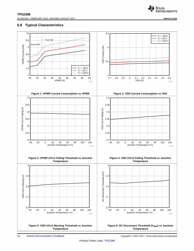
6.8 Typical Characteristics
Figure 1. VPWR Current Consumption vs VPWR Figure 2. VDD Current Consumption vs VDD
Figure 3. VPWR UVLO Falling Threshold vs JunctionTemperature
Figure 4. VDD UVLO Falling Threshold vs JunctionTemperature
Figure 5. VDD UVLO Warning Threshold vs JunctionTemperature
Figure 6. DC Disconnect Threshold (VIMIN) vs JunctionTemperature
FET VDS (V)
Cur
rent
Lim
it T
hres
hold
(m
V)
0 10 20 30 40 500
50
100
150
200
250
300
D011
1x2x
Junction Temperature (qC)
Cur
rent
Lim
it T
hres
hold
(m
V)
-40 -20 0 20 40 60 80 100 120270
272
274
276
278
280
D009Port Voltage (V)
Inru
sh L
imit
Thr
esho
ld (
mV
)
0 10 20 30 40 500
10
20
30
40
50
60
70
80
90
100
110
120
D010
Classification Current (mA)
Cla
ssifi
catio
n V
olta
ge (
V)
0 10 20 30 40 50 60 70 8012
14
16
18
20
22
D007
TJ = -40qCTJ = 25qCTJ = 125qC
Junction Temperature (qC)
Cur
rent
Lim
it T
hres
hold
(m
V)
-40 -20 0 20 40 60 80 100 120105
106
107
108
109
110
D008
13
TPS2388www.ti.com SLUSC25A –FEBRUARY 2015–REVISED AUGUST 2017
Product Folder Links: TPS2388
Submit Documentation FeedbackCopyright © 2015–2017, Texas Instruments Incorporated
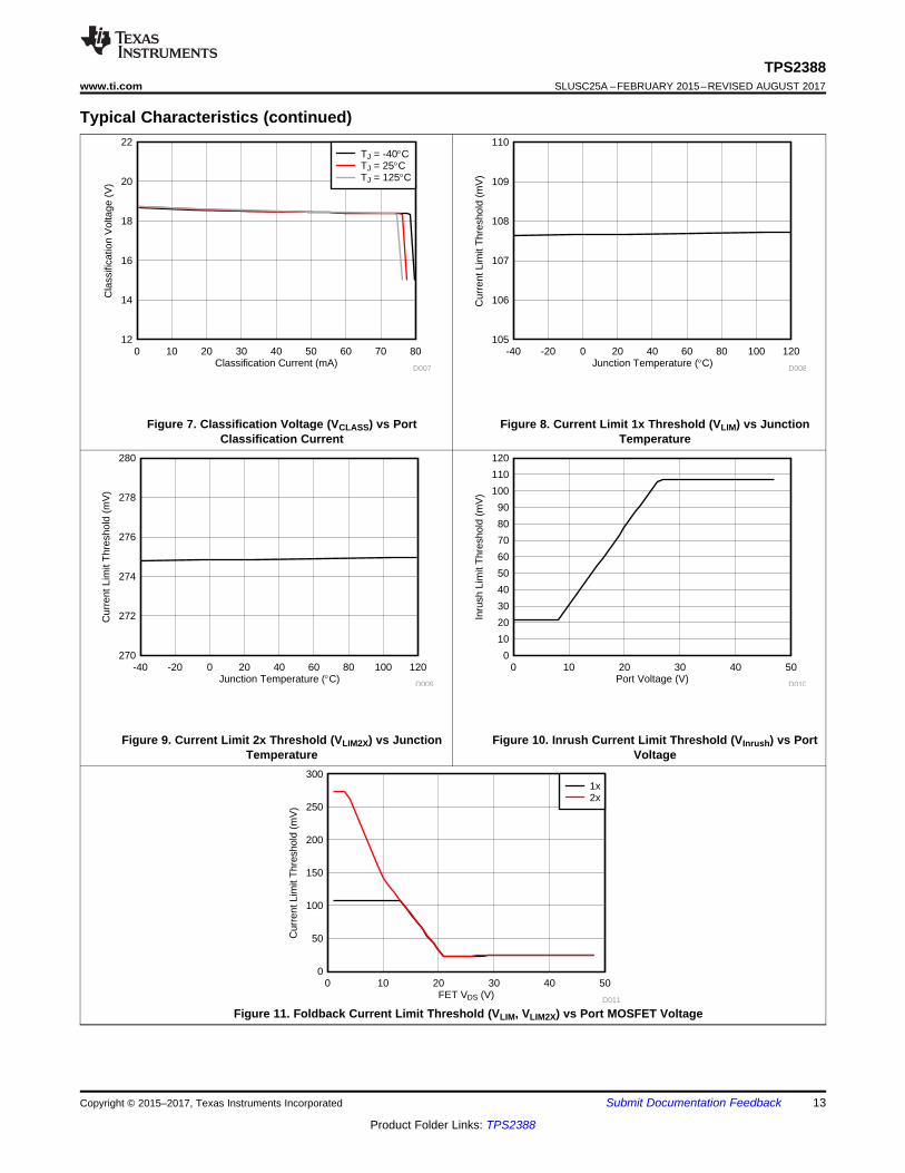
Typical Characteristics (continued)
Figure 7. Classification Voltage (VCLASS) vs PortClassification Current
Figure 8. Current Limit 1x Threshold (VLIM) vs JunctionTemperature
Figure 9. Current Limit 2x Threshold (VLIM2X) vs JunctionTemperature
Figure 10. Inrush Current Limit Threshold (VInrush) vs PortVoltage
Figure 11. Foldback Current Limit Threshold (VLIM, VLIM2X) vs Port MOSFET Voltage
Four-point detection
Class
Port turn-on
tDETtpdc
tpon
VPORT 0V
VCLASS
tfSDA tfo
Repeated Start Condition
tLOWtSU,DAT
tHD,DAT
SCL
SDAI/SDAO
tr tf
trSDA
tHIGH
Start Condition Stop Condition
Start Condition
tSU,STOtHD,STA tSU,STA
tBUF
14
TPS2388SLUSC25A –FEBRUARY 2015–REVISED AUGUST 2017 www.ti.com
Product Folder Links: TPS2388
Submit Documentation Feedback Copyright © 2015–2017, Texas Instruments Incorporated
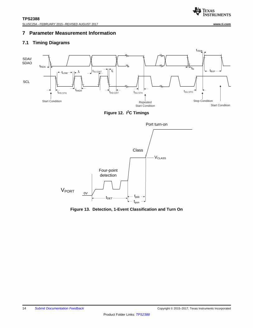
7 Parameter Measurement Information
7.1 Timing Diagrams
Figure 12. I2C Timings
Figure 13. Detection, 1-Event Classification and Turn On
SEN
GATE
0 V
0 V
VLIM
VCUT
tOVLD
tpon
VPORT 0 V
Four-point detection
tDETtCLE
tME
ClassVCLASS
VMARK
Mark
Port turn-on
15
TPS2388www.ti.com SLUSC25A –FEBRUARY 2015–REVISED AUGUST 2017
Product Folder Links: TPS2388
Submit Documentation FeedbackCopyright © 2015–2017, Texas Instruments Incorporated
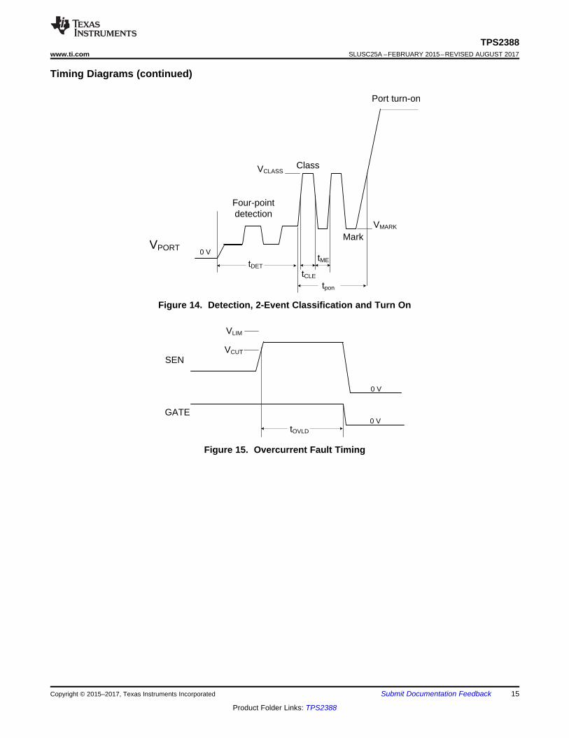
Timing Diagrams (continued)
Figure 14. Detection, 2-Event Classification and Turn On
Figure 15. Overcurrent Fault Timing

16
TPS2388SLUSC25A –FEBRUARY 2015–REVISED AUGUST 2017 www.ti.com
Product Folder Links: TPS2388
Submit Documentation Feedback Copyright © 2015–2017, Texas Instruments Incorporated
8 Detailed Description
8.1 OverviewThe TPS2388 is an eight-port PSE for power over Ethernet applications. Each of the eight ports providesdetection, classification, protection, and shut down in compliance with the IEEE 802.3at standard.
Basic PoE features include the following:• Performs high-reliability 4-point load detection• Performs classification including type-2 (two-finger) of up to Class 4 loads• Enables power with protective foldback current limiting, and adjustable ICUT threshold• Shuts down in the event of fault loads and shorts• Performs maintain power signature function to ensure removal of power if load is disconnected• Undervoltage lockout occurs if VPWR falls below VPUV_F (typical 26.5 V).
Enhanced features include the following:• Port re-mapping capability• 8- and 16-bit access mode selectable• 1- and 3-bit port shutdown priority• Port turn ON command automatically supports IEEE TPON specification (0x23 register or 0x19 and 0x40
register)
Following a power-off command, disconnect, or shutdown due to a start, ICUT, or ILIM fault, the port powersdown. Following port power off due to a power off command or disconnect, the TPS2388 restarts a detectioncycle if commanded to do so. If the shutdown is due to a start, ICUT, or ILIM fault, the TPS2388 first enters intoa cool-down period, at the end of this period the TPS2388 is able to restart the detection cycle.
Using the turn ON command supporting TPON, the TPS2388 will not automatically apply power to a port underthe following circumstances:• The detect status is not resistance valid.• If the classification status is overcurrent, class mismatch, or unknown.
Common Functions for Ports 5-8
Common Functions for Ports1-4
Port 2-8 Analog Control Functions
Port 1 Analog Control Functions
RA
NG
E
SE
LEC
T 14-23 Bit ADC
(Current)
2X Power
12V Regulator
ICLASS
5V Regulator2.5V Precision Reference
Internal Rails Good
Temp
VEE
Vds
1.8V Logic5V Logic
5 or 12V Analog80V Analog
BIT
4:1 MUX
V48
PTAT DIODES
Analog BIT MUX
RA
NG
E
SE
LEC
T
14-23 Bit ADC
(Voltage)
Variable Averager
Legend
Vdisco
GmDRIVER
DRAIN1-4PORT DIFF AMP
V48
Vport
Foldback Schedulers
Fast Ishort Protectiondv/dt ramping control
Rapid Overload recoveryGATEx
Enable
SENx
Ilim
320Hz LPFIPORT
BIT
DIS
CR
ET
E IO
CO
ND
ITIO
NE
RS
RST to blks
CPU Watchdog
Register File
I2C Interface
External Data Memory Bus
CPU
Interrupt Controller
De-bugger
7 bit address Select
JTAG
Timer 0
Timer 1
SFR
BUS
8051 WARP
Scan + Digital Test
SCL Watchdog
256 ByteCPU SRAM
(00-FF)
32KVIA ROM
IRAMBus
ProgMemBus
Mem
ory
BIS
T
Int/E
xt R
OM
Sel
Pad Field for EXT Flash8 data, 14 address, Enable, Testmode
GND, 1.8V, 10 ProbeIO
Bus
IF
OTP TRIM56 Byte
Class Current LimitClass Port Voltage Control
Variable Averager
8V OTP Supply
JTAG(1-4)
SDAISDAO
SCL
Firmware Controlled Update from register File
1.8V LDO VDD UVLO
VDD
1.8V Logic Supply
14MHz Internal Oscillator
RESETB OSS
RST BlockPG
CLK OK
Clock Distribution
DRAINx
11.5V 5.0V 2.5VREF
8V
KSENSEx
CLK to blks
CLK OK
PG
OSS
INT
A1-A4
ATEST
0.255
OSS/POR
PD LOAD
VPWR
IDET
Analog Test
DTEST Digital Test MuxA/D Timing/Foldback + I2C Signals
FW Registers
128 ByteSFR
(80-FF)With BIST
7.5/2.8MHz
REMAP
Clock/128 and WD
TCLKTMS
TCLKTDO
Analog Register
IO
Fuse-able Disconnect
VPWR VPWR Divider
VPWR
NC
VPWR
1/31/3 2/3 2/32.5VREF
NC NCNC
1024 ByteCode Substitution OTPwith 1024/3 Patch
Space
Load at Power up into holding latches
Copyright © 2017, Texas Instruments Incorporated
TPS2388www.ti.com SLUSC25A –FEBRUARY 2015–REVISED AUGUST 2017
17
Product Folder Links: TPS2388
Submit Documentation FeedbackCopyright © 2015–2017, Texas Instruments Incorporated
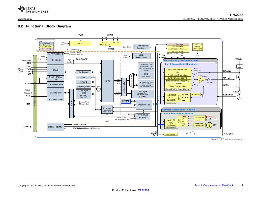
8.2 Functional Block Diagram
IDLE
START bits
SC 2
one-bit duration
tbit_OSS
tOSS_IDL
3.3 V
0 V
SC 1OSS SC 0
Shutdown Code
GATE
tOSS_OFF
IDLE
tr_OSS
tf_OSS
18
TPS2388SLUSC25A –FEBRUARY 2015–REVISED AUGUST 2017 www.ti.com
Product Folder Links: TPS2388
Submit Documentation Feedback Copyright © 2015–2017, Texas Instruments Incorporated
8.3 Feature Description
8.3.1 Port RemappingThe TPS2388 provides port remapping capability, from the logical ports to the physical ports/pins.
The remapping is between any port of a 4-port group (1 to 4, 5 to 8).
The following example is applicable to 0x26 register = 00111001, 00111001b.• Logical port 1 (5) ↔ Physical port 2 (6)• Logical port 2 (6) ↔ Physical port 3 (7)• Logical port 3 (7) ↔ Physical port 4 (8)• Logical port 4 (8) ↔ Physical port 1 (5)
NOTEThe device ignores any remapping command unless all four ports are in off mode.
If the TPS2388 receives an incorrect configuration, it simply ignores the incorrect configuration and keeps theconfiguration unchanged. The ACK is also sent as usual at the end of communication. For example, if the samecode is received for more than one port, then a read back of the Re-Mapping register (0x26) would be the lastvalid configuration.
Also note that if an IC reset command (1Ah register) is received, the port remapping configuration is keptunchanged. However, if there is a Power-on Reset or if the RESET pin is activated, the Re-Mapping register isreinitialized to a default value.
8.3.2 Port Power PriorityThe TPS2388 supports 1- and 3-bit shutdown priority, selectable with the MbitPrty bit of General Mask register(0x17).
The 1-bit shutdown priority works with the Port Power Priority (0x15) register. An OSSn bit with a value of 1indicates that the corresponding port will be treated as low priority, while a value of 0 corresponds to a highpriority. As soon as the OSS input goes high, the low-priority ports are turned off.
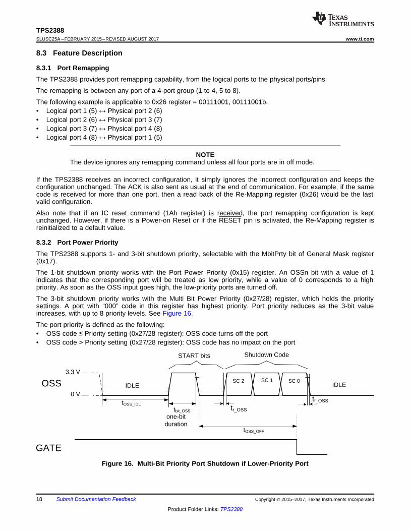
The 3-bit shutdown priority works with the Multi Bit Power Priority (0x27/28) register, which holds the prioritysettings. A port with “000” code in this register has highest priority. Port priority reduces as the 3-bit valueincreases, with up to 8 priority levels. See Figure 16.
The port priority is defined as the following:• OSS code ≤ Priority setting (0x27/28 register): OSS code turns off the port• OSS code > Priority setting (0x27/28 register): OSS code has no impact on the port
Figure 16. Multi-Bit Priority Port Shutdown if Lower-Priority Port
19
TPS2388www.ti.com SLUSC25A –FEBRUARY 2015–REVISED AUGUST 2017
Product Folder Links: TPS2388
Submit Documentation FeedbackCopyright © 2015–2017, Texas Instruments Incorporated
Feature Description (continued)
NOTEPrior to setting the MbitPrty bit from 0 to 1, make sure the OSS input is in the idle (low)state for a minimum of 200 µs, to avoid any port misbehavior related to loss ofsynchronization with the OSS bit stream.
NOTEThe OSS input has an internal 1-µs to 5-µs deglitch filter. From the idle state, a pulse witha longer duration is interpreted as a valid start bit. Ensure that the OSS signal is noisefree.
8.3.3 A/D ConverterThe TPS2388 features ten multi-slope integrating converters. Each of the first eight converters is dedicated tocurrent measurement for one port and is operated independently to perform measurements in any of thefollowing modes: classification and port powered. When the port is powered, the converter is used for current(100-ms averaged) monitoring, port policing, and DC disconnect. Each of the last two converters are sharedwithin a group of four ports for discovery (16.6-ms averaged), port powered voltage monitoring, Power Goodstatus, and FET short detection. It is also used for general-purpose measurements including input voltage (1 ms)and temperature.
The A/D converter type used in the TPS2388 differs from other similar types of converters in that it convertswhile the input signal is being sampled by the integrator, providing inherent filtering over the conversion period.The typical conversion time of the current converters is 800 µs, while it is 1 ms for the other converters.Powered-device detection is performed by averaging 16 consecutive samples providing significant rejection ofnoise at 50-Hz or 60-Hz line frequency. While a port is powered, digital averaging is used to provide a portcurrent measurement integrated over a 100-ms time period. Note also that an anti-aliasing filter is present forport powered current monitoring.
NOTEDuring port-powered mode, port current conversions are performed continuously. Also, inport-powered mode, the tSTART timer must expire before any current or voltage A/Dconversion can begin.
8.3.4 I2C WatchdogAn I2C Watchdog timer is available on the TPS2388 device. The timer monitors the I2C, SCL line for clock edges.When enabled, a timeout of the watchdog resets the I2C interface along with any active ports. This featureprovides protection in the event of a hung software situation or I2C bus hang-up by slave devices. In the lattercase, if a slave is attempting to send a data bit of 0 when the master stops sending clocks, then the slave couldget stuck driving the data line low indefinitely. Because the data line is being driven low, the master cannot senda STOP to clean up the bus. Activating the I2C watchdog feature of the TPS2388 would clear this deadlockedcondition. If the timer of 2 seconds expires, the ports latch off and the WD Status bit is set. Note that WD Statuswill be set even if the watchdog is not enabled. WD Status can only be cleared by a reset or writing a 0 to theWDS status bit location. The 4-bit watchdog disable field shuts down this feature when a code of 1011b isloaded. This field is preset to 1011b whenever the TPS2388 is initially powered. Also see I2C WATCHDOGRegister for more details.
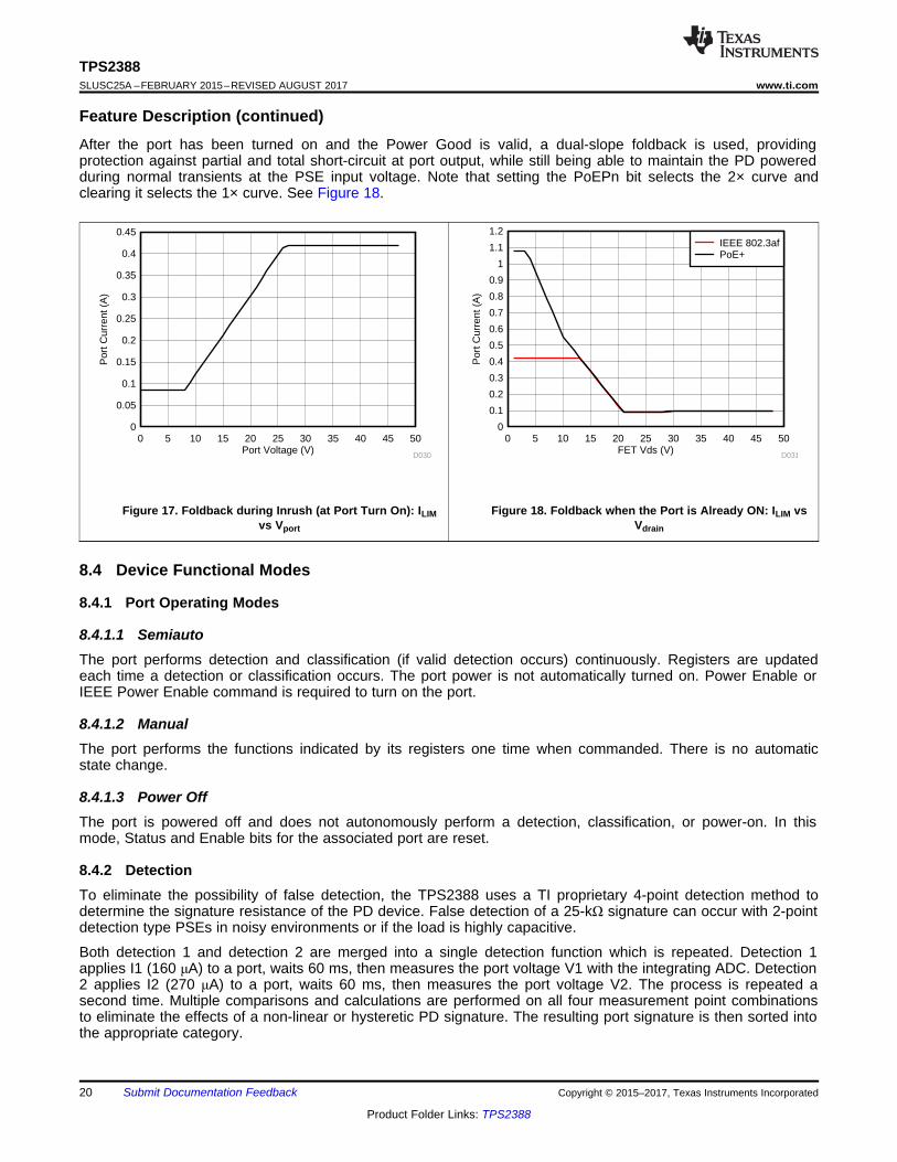
8.3.5 Foldback ProtectionThe TPS2388 features two types of foldback protection mechanisms for complete MOSFET protection. Duringinrush at port turn on, the foldback is based on the port voltage as shown in Figure 17. Note that the inrushcurrent profile remains the same, whatever the state of the PoEPn bit in the PoE Plus register.
Port Voltage (V)
Por
t Cur
rent
(A
)
0 5 10 15 20 25 30 35 40 45 500
0.05
0.1
0.15
0.2
0.25
0.3
0.35
0.4
0.45
D030FET Vds (V)
Por
t Cur
rent
(A
)
0 5 10 15 20 25 30 35 40 45 500
0.1
0.2
0.3
0.4
0.5
0.6
0.7
0.8
0.9
1
1.1
1.2
D031
IEEE 802.3afPoE+
20
TPS2388SLUSC25A –FEBRUARY 2015–REVISED AUGUST 2017 www.ti.com
Product Folder Links: TPS2388
Submit Documentation Feedback Copyright © 2015–2017, Texas Instruments Incorporated
Feature Description (continued)After the port has been turned on and the Power Good is valid, a dual-slope foldback is used, providingprotection against partial and total short-circuit at port output, while still being able to maintain the PD poweredduring normal transients at the PSE input voltage. Note that setting the PoEPn bit selects the 2× curve andclearing it selects the 1× curve. See Figure 18.
Figure 17. Foldback during Inrush (at Port Turn On): ILIMvs Vport
Figure 18. Foldback when the Port is Already ON: ILIM vsVdrain
8.4 Device Functional Modes
8.4.1 Port Operating Modes
8.4.1.1 SemiautoThe port performs detection and classification (if valid detection occurs) continuously. Registers are updatedeach time a detection or classification occurs. The port power is not automatically turned on. Power Enable orIEEE Power Enable command is required to turn on the port.
8.4.1.2 ManualThe port performs the functions indicated by its registers one time when commanded. There is no automaticstate change.
8.4.1.3 Power OffThe port is powered off and does not autonomously perform a detection, classification, or power-on. In thismode, Status and Enable bits for the associated port are reset.
8.4.2 DetectionTo eliminate the possibility of false detection, the TPS2388 uses a TI proprietary 4-point detection method todetermine the signature resistance of the PD device. False detection of a 25-kΩ signature can occur with 2-pointdetection type PSEs in noisy environments or if the load is highly capacitive.
Both detection 1 and detection 2 are merged into a single detection function which is repeated. Detection 1applies I1 (160 μA) to a port, waits 60 ms, then measures the port voltage V1 with the integrating ADC. Detection2 applies I2 (270 μA) to a port, waits 60 ms, then measures the port voltage V2. The process is repeated asecond time. Multiple comparisons and calculations are performed on all four measurement point combinationsto eliminate the effects of a non-linear or hysteretic PD signature. The resulting port signature is then sorted intothe appropriate category.

21
TPS2388www.ti.com SLUSC25A –FEBRUARY 2015–REVISED AUGUST 2017
Product Folder Links: TPS2388
Submit Documentation FeedbackCopyright © 2015–2017, Texas Instruments Incorporated
Device Functional Modes (continued)
NOTEThe detection resistance measurement result is also available in the Port DetectResistance register.
8.4.3 ClassificationHardware classification (class) is performed by supplying a voltage and sampling the resulting current. Toeliminate the high power of a classification event from occurring in the power controller chip, the TPS2388 makesuse of the external power FET for classification.
During classification, the voltage on the gate node of the external MOSFET is part of a linear control loop. Thecontrol loop applies the appropriate MOSFET drive to maintain a differential voltage between VPWR and DRAINof 17.5 V. During classification the voltage across the sense resistor in the source of the MOSFET is measuredand converted to a class level within the TPS2388. If a load short occurs during classification, the MOSFET gatevoltage is quickly reduced to a linearly controlled, short-circuit value for the duration of the class event.
Classification results may be read through the I2C Detection Event and Port n Status Registers. The TPS2388also supports two-event classification for type 2 PDs, using the IEEE Power Enable register.
8.4.4 DC DisconnectDisconnect is the automated process of turning off power to the port. When the port is unloaded or at least fallsbelow minimum load, it is necessary to turn off power to the port and restart detection. In DC disconnect, thevoltage across the sense resistors is measured. When enabled, the DC disconnect function monitors the senseresistor voltage of a powered port to verify the port is drawing at least the minimum current to remain active. TheTDIS timer counts up whenever the port current is below a 7.5-mA threshold. If a timeout occurs, the port is shutdown and the corresponding disconnect bit in the Fault Event Register is set. The TDIS counter is reset eachtime the current goes continuously higher than the disconnect threshold for nominally 15 ms.
The TDIS duration is set by the TMPDO Bits of the Timing Configuration register (0x16).
8.5 Programming
8.5.1 I2C Serial InterfaceThe TPS2388 features a 3-wire I2C interface, using SDAI, SDAO, and SCL. Each transmission includes a Startcondition sent by the master, followed by the device address (7-bit) with R/W bit, a register address byte, thenone or two data bytes and a Stop condition. The recipient also sends an acknowledge bit following each bytetransmitted. Also, SDAI/SDAO is stable while SCL is high except during a Start or Stop condition.
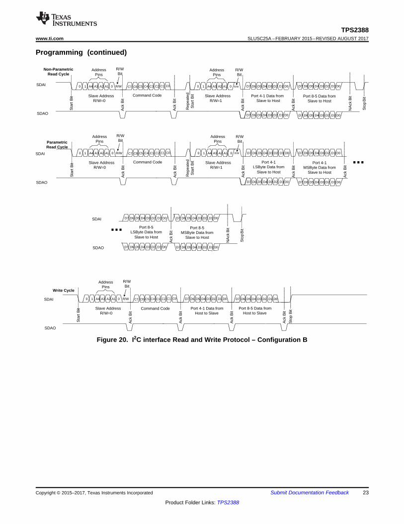
Figure 19 and Figure 20 illustrate read and write operations through I2C interface, using configuration A or B (seeTable 19 for more details). The 'parametric' read operation is applicable to A/D conversion results. The TPS2388also features quick access to the latest addressed register through I2C bus. This means that when a Stop bit isreceived, the register pointer is not automatically reset.
It is also possible to perform a write operation to many TPS2388 devices at the same time. The slave addressduring this broadcast access is 0x7F, as shown in Pin Status Register. Depending on which configuration (A orB) is selected, a global write proceeds as following:• Config A: Both 4-port devices (1 to 4 and 5 to 8) are addressed at same time.• Config B: The whole device is addressed.

Write Cycle
0 1 A4 A3 A2 A1 A0 R/W D7 D6 D5 D4 D3 D2 D1 D0
Sta
rt B
it Slave AddressR/W=0
R/WBit
Data fromHost to Slave
Sto
p B
it
Ack
Bit
Ack
Bit
Ack
Bit
C7 C6 C5 C4 C3 C2 C1 C0
Command Code
0 1 A4 A3 A2 A1 A0 R/W 0 1 A4 A3 A2 A1 A0 R/W
D7 D6 D5 D4 D3 D2 D1 D0
R/WBit
Sta
rt B
it Slave AddressR/W=0
Command Code Slave AddressR/W=1
R/WBit
Data fromSlave to Host
Ack
Bit
Ack
Bit
Ack
Bit
NA
ck B
it
Sto
p B
it
C7 C6 C5 C4 C3 C2 C1 C0 D7 D6 D5 D4 D3 D2 D1 D0
Non-Parametric Read Cycle
Parametric Read Cycle
SDAO
0 1 A4 A3 A2 A1 A0 R/W 0 1 A4 A3 A2 A1 A0R/W
D7 D6 D5 D4 D3 D2 D1 D0
R/WBit
Sta
rt B
it Slave AddressR/W=0
Command Code Slave AddressR/W=1
R/WBit
LSByte Data fromSlave to Host
Ack
Bit
Ack
Bit
Bit
SDAI
NA
ck B
it
Sto
p B
it
C7 C6 C5 C4 C3 C2 C1 C0
Ack
Bit
Ack
D7 D6 D5 D4 D3 D2 D1 D0
D7 D6 D5 D4 D3 D2 D1 D0 D7 D6 D5 D4 D3 D2 D1 D0
SDAO
SDAI
SDAO
SDAI
Rep
eate
d S
tart
Bit
Rep
eate
d S
tart
Bit MSByte Data from
Slave to Host
0 1 A4 A3 A2 A1 A0 R/W
D7 D6 D5 D4 D3 D2 D1 D0
Slave AddressR/W=1
R/WBit
Data fromSlave to Host
Sta
rt B
it
Ack
Bit
NA
ck B
it
Sto
p B
it
D7 D6 D5 D4 D3 D2 D1 D0
Quick Read Cycle (latest addressed register)
SDAO
SDAI
Address Pins
Address Pins
Address Pins
Address Pins
Address Pins
Address Pins
22
TPS2388SLUSC25A –FEBRUARY 2015–REVISED AUGUST 2017 www.ti.com
Product Folder Links: TPS2388
Submit Documentation Feedback Copyright © 2015–2017, Texas Instruments Incorporated
Programming (continued)
Figure 19. I2C interface Read and Write Protocol – Configuration A
Write Cycle
0 1 A4 A3 A2 A1 0 R/W D7 D6 D5 D4 D3 D2 D1 D0
Sta
rt B
it Slave AddressR/W=0
R/WBit
Port 4-1 Data fromHost to Slave
Sto
p B
it
Ack
Bit
Ack
Bit
Ack
Bit
C7 C6 C5 C4 C3 C2 C1 C0
Command Code
0 1 A4 A3 A2 A1 0 R/W 0 1 A4 A3 A2 A1 0 R/W
D7 D6 D5 D4 D3 D2 D1 D0
R/WBit
Sta
rt B
it Slave AddressR/W=0
Command Code Slave AddressR/W=1
R/WBit
Port 4-1 Data fromSlave to Host
Ack
Bit
Ack
Bit
Ack
Bit
C7 C6 C5 C4 C3 C2 C1 C0 D7 D6 D5 D4 D3 D2 D1 D0
Non-Parametric Read Cycle
Parametric Read Cycle
SDAO
0 1 A4 A3 A2 A1 0 R/W 0 1 A4 A3 A2 A1 0 R/W
D7 D6 D5 D4 D3 D2 D1 D0
R/WBit
Sta
rt B
it Slave AddressR/W=0
Command Code Slave AddressR/W=1
R/WBit
Port 4-1 LSByte Data from
Slave to Host
Ack
Bit
Ack
Bit
Bit
SDAI C7 C6 C5 C4 C3 C2 C1 C0
Ack
Bit
Ack
D7 D6 D5 D4 D3 D2 D1 D0
D7 D6 D5 D4 D3 D2 D1 D0 D7 D6 D5 D4 D3 D2 D1 D0
SDAO
SDAI
SDAO
SDAI
Rep
eate
d S
tart
Bit
Rep
eate
d S
tart
Bit Port 4-1
MSByte Data fromSlave to Host
Address Pins
Address Pins
NA
ck B
it
Sto
p B
it
Bit
Ack
D7 D6 D5 D4 D3 D2 D1 D0
D7 D6 D5 D4 D3 D2 D1 D0
Port 8-5 Data fromSlave to Host
Address Pins
Address Pins
D7 D6 D5 D4 D3 D2 D1 D0
Port 8-5 LSByte Data from
Slave to Host
NA
ck B
it
Sto
p B
it
Bit
Ack
D7 D6 D5 D4 D3 D2 D1 D0
D7 D6 D5 D4 D3 D2 D1 D0 D7 D6 D5 D4 D3 D2 D1 D0
Port 8-5MSByte Data from
Slave to Host
SDAO
SDAI
Ack
Bit
...
...
Address Pins
D7 D6 D5 D4 D3 D2 D1 D0
Ack
Bit
Port 8-5 Data fromHost to Slave
23
TPS2388www.ti.com SLUSC25A –FEBRUARY 2015–REVISED AUGUST 2017
Product Folder Links: TPS2388
Submit Documentation FeedbackCopyright © 2015–2017, Texas Instruments Incorporated
Programming (continued)
Figure 20. I2C interface Read and Write Protocol – Configuration B

TPS2388SLUSC25A –FEBRUARY 2015–REVISED AUGUST 2017 www.ti.com
24
Product Folder Links: TPS2388
Submit Documentation Feedback Copyright © 2015–2017, Texas Instruments Incorporated
(1) SUPF bit reset state shown is at Power up only(2) VDUV, VPUV and VDWRN bits reset state shown is at Power up only
8.6 Register Maps
8.6.1 Complete Register Set
Table 1. Main RegistersCmdCode
Register orCommand Name
I2CR/W
DataByte RST State Bits Description
INTERRUPTS
00h INTERRUPT RO 1 1000,0000b (1) SUPF STRTF IFAULT CLASC DETC DISF PGC PEC
01h INTERRUPT MASK R/W 1 1000,0000b SUMSK STMSK IFMSK CLMSK DEMSK DIMSK PGMSK PEMSK
EVENT
02hPOWER EVENT
RO 10000,0000b
Power Good status change Power Enable status change
03h CoR 1 PGC4 PGC3 PGC2 PGC1 PEC4 PEC3 PEC2 PEC1
04hDETECTION EVENT
RO 10000,0000b
Classification Detection
05h CoR 1 CLSC4 CLSC3 CLSC2 CLSC1 DETC4 DETC3 DETC2 DETC1
06hFAULT EVENT
RO 10000,0000b
Disconnect occurred ICUT fault occurred
07h CoR 1 DISF4 DISF3 DISF2 DISF1 ICUT4 ICUT3 ICUT2 ICUT1
08hSTART/ILIM EVENT
RO 10000,0000b
ILIM fault occurred START fault occurred
09h CoR 1 ILIM4 ILIM3 ILIM2 ILIM1 STRT4 STRT3 STRT2 STRT1
0AhSUPPLY EVENT
RO 10111,0000b (2) TSD VDUV VDWRN VPUV Rsvd Rsvd Rsvd Rsvd
0Bh CoR 1
STATUS
0Ch PORT 1 STATUS RO 1 0000,0000b Rsvd CLASS Port 1 DETECT Port 1
0Dh PORT 2 STATUS RO 1 0000,0000b Rsvd CLASS Port 2 DETECT Port 2
0Eh PORT 3 STATUS RO 1 0000,0000b Rsvd CLASS Port 3 DETECT Port 3
0Fh PORT 4 STATUS RO 1 0000,0000b Rsvd CLASS Port 4 DETECT Port 4
10h POWER STATUS RO 1 0000,0000b PG4 PG3 PG2 PG1 PE4 PE3 PE2 PE1
11h PIN STATUS RO 1 0,A[4:0],0,0 Rsvd SLA4 SLA3 SLA2 SLA1 SLA0 Rsvd Rsvd
CONFIGURATION
12h OPERATING MODE R/W 1 0000,0000b Port 4 Mode Port 3 Mode Port 2 Mode Port 1 Mode
13h DISCONNECT ENABLE R/W 1 0000,0000b Rsvd Rsvd Rsvd Rsvd DCDE4 DCDE3 DCDE2 DCDE1
14h DETECT/CLASSENABLE R/W 1 0000,0000b CLE4 CLE3 CLE2 CLE1 DETE4 DETE3 DETE2 DETE1
15h PWRPR/ICUT DISABLE R/W 1 0000,0000b OSS4 OSS3 OSS2 OSS1 DCUT4 DCUT3 DCUT2 DCUT1
16h TIMING CONFIG R/W 1 0000,0000b TLIM TSTART TOVLD TMPDO
17h GENERAL MASK R/W 1 1000,0000b INTEN Rsvd nbitACC MbitPrty CLCHE DECHE Rsvd

TPS2388www.ti.com SLUSC25A –FEBRUARY 2015–REVISED AUGUST 2017
25
Product Folder Links: TPS2388
Submit Documentation FeedbackCopyright © 2015–2017, Texas Instruments Incorporated
Register Maps (continued)Table 1. Main Registers (continued)
CmdCode
Register orCommand Name
I2CR/W
DataByte RST State Bits Description
PUSH BUTTONS
18h DETECT/CLASS Restart WO 1 0000,0000b RCL4 RCL3 RCL2 RCL1 RDET4 RDET3 RDET2 RDET1
19h POWER ENABLE WO 1 0000,0000b POFF4 POFF3 POFF2 POFF1 PWON4 PWON3 PWON2 PWON1
1Ah RESET WO 1 0000,0000b CLRAIN CLINP Rsvd RESAL RESP4 RESP3 RESP2 RESP1
GENERAL/SPECIALIZED
1Bh ID RO 1 Mf[4:0],IC[2:0] MFR ID IC Version
1Ch Reserved CoR 1 0000,0000b Reserved Reserved
1Eh POLICE 21 CONFIG R/W 1 1111,1111b POLICE Port 2 POLICE Port 1
1Fh POLICE 43 CONFIG R/W 1 1111,1111b POLICE Port 4 POLICE Port 3
23h IEEE Power Enable WO 1 0000,0000b T2PON4 T2PON3 T2PON2 T2PON1 T1PON4 T1PON3 T1PON2 T1PON1
24hPower-on FAULT
RO 10000,0000b PF Port 4 PF Port 3 PF Port 2 PF Port 1
25h CoR 1
26h RE-MAPPING R/W 1 1110,0100b Physical re-map Logical Port 4 Physical re-map Logical Port3
Physical re-map Logical Port2 Physical re-map Logical Port 1
27h Multi-bit Power Priority21 R/W 1 0000,0000b Rsvd Port 2 Rsvd Port 1
28h Multi-bit Power Priority43 R/W 1 0000,0000b Rsvd Port 4 Rsvd Port 3
29h-2Bh Reserved R/W 1 0000,0000b Rsvd Rsvd Rsvd Rsvd Rsvd Rsvd Rsvd Rsvd
2Ch TEMPERATURE RO 1 0000,0000b Temperature (bits 7 to 0)
2EhINPUT VOLTAGE
RO2
0000,0000b Input Voltage: LSByte
2Fh RO 0000,0000b Rsvd Rsvd Input Voltage: MSByte (bits 13 to 8)
EXTENDED REGISTER SET – PORT PARAMETRIC MEASUREMENT
30hPORT 1 CURRENT
RO2
0000,0000b Port 1 Current: LSByte
31h RO 0000,0000b Rsvd Rsvd Port 1 Current: MSByte (bits 13 to 8)
32hPORT 1 VOLTAGE
RO2
0000,0000b Port 1 Voltage: LSByte
33h RO 0000,0000b Rsvd Rsvd Port 1 Voltage: MSByte (bits 13 to 8)

TPS2388SLUSC25A –FEBRUARY 2015–REVISED AUGUST 2017 www.ti.com
26
Product Folder Links: TPS2388
Submit Documentation Feedback Copyright © 2015–2017, Texas Instruments Incorporated
Table 2. Main RegistersCmdCode
Register orCommand Name I2C R/W Data
Byte RST State Bits Description
34hPORT 2 CURRENT
RO2
0000,0000b Port 2 Current: LSByte
35h RO 0000,0000b Rsvd Rsvd Port 2 Current: MSByte (bits 13 to 8)
36hPORT 2 VOLTAGE
RO2
0000,0000b Port 2 Voltage: LSByte
37h RO 0000,0000b Rsvd Rsvd Port 2 Voltage: MSByte (bits 13 to 8)
38hPORT 3 CURRENT
RO2
0000,0000b Port 3 current: LSByte
39h RO 0000,0000b Rsvd Rsvd Port 3 Current: MSByte (bits 13 to 8)
3AhPORT 3 VOLTAGE
RO2
0000,0000b Port 3 Voltage: LSByte
3Bh RO 0000,0000b Rsvd Rsvd Port 3 Voltage: MSByte (bits 13 to 8)
3ChPORT 4 CURRENT
RO2
0000,0000b Port 4 current: LSByte
3Dh RO 0000,0000b Rsvd Rsvd Port 4 Current: MSByte (bits 13 to 8)
3EhPORT 4 VOLTAGE
RO2
0000,0000b Port 4 Voltage: LSByte
3Fh RO 0000,0000b Rsvd Rsvd Port 4 Voltage: MSByte (bits 13 to 8)
CONFIGURATION/OTHERS
40h PoE PLUS R/W 1 0000,0000b PoEP4 PoEP3 PoEP2 PoEP1 Rsvd Rsvd Rsvd TPON
41h FIRMWARE REVISION RO 1 RRRR,RRRRb Firmware Revision
42h I2C WATCHDOG R/W 1 0001,0110b Rsvd Rsvd Rsvd Watchdog Disable WDS
43h DEVICE ID RO 1 110,sr[4:0] Device ID number Silicon Revision number
PORT SIGNATURE MEASUREMENTS
44h P1 DETECTRESISTANCE RO 1 0000,0000b Port 1 Resistance
45h P2 DETECTRESISTANCE RO 1 0000,0000b Port 2 Resistance
46h P3 DETECTRESISTANCE RO 1 0000,0000b Port 3 Resistance
47h P4 DETECTRESISTANCE RO 1 0000,0000b Port 4 Resistance
48h-6Fh Reserved R/W 1 0000,0000b Reserved

TPS2388www.ti.com SLUSC25A –FEBRUARY 2015–REVISED AUGUST 2017
27
Product Folder Links: TPS2388
Submit Documentation FeedbackCopyright © 2015–2017, Texas Instruments Incorporated
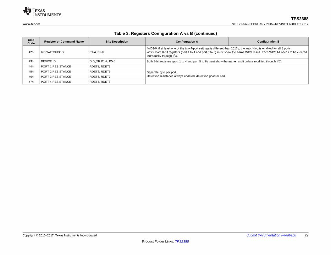
Table 3. Registers Configuration A vs BCmdCode Register or Command Name Bits Description Configuration A Configuration B
00h INTERRUPT INT bits P1-4, P5-8 Separate mask and interrupt result per group of 4 ports.The Supply event bit is repeated twice.01h INTERRUPT MASK MSK bits P1-4, P5-8
02hPOWER EVENT PGC_PEC P4-1, P8-5
Separate event byte per group of 4 ports.
03h
04hDETECTION EVENT CLS_DET P4-1, P8-5
05h
06hFAULT EVENT DIS_ICUT P4-1, P8-5
07h
08hSTART/ILIM EVENT ILIM_STR P4-1, P8-5
09h
0AhSUPPLY EVENT TSD, VDUV, VDUW, VPUV Both 8-bit registers (port 1 to 4 and port 5 to 8) must show the same result.
Clearing at least one VPUV/VDUV also clears the other one.0Bh
0Ch PORT 1 STATUS CLS&DET1_CLS&DET5
Separate Status byte per port0Dh PORT 2 STATUS CLS&DET2_CLS&DET6
0Eh PORT 3 STATUS CLS&DET3_CLS&DET7
0Fh PORT 4 STATUS CLS&DET4_CLS&DET8
10h POWER STATUS PG_PE P4-1, P8-5 Separate status byte per group of 4 ports
11h PIN STATUS A4-A1,A0Both 8-bit registers (port 1 to 4 and port 5 to 8) must showthe same result, except that A0 = 0 (port 1 to 4) or 1 (port 5to 8).
Both 8-bit registers (port 1 to 4 and port 5 to 8) must showthe same result, including A0 = 0.
12h OPERATING MODE MODE P4-1, P8-5 Separate Mode byte per group of 4 ports.
13h DISCONNECT ENABLE DCDE P4-1, P8-5 Separate DC disconnect enable byte per group of 4 ports.
14h DETECT/CLASS ENABLE CLE_DETE P4-1, P8-5 Separate Detect/Class Enable byte per group of 4 ports.
15h PWRPR/ICUT DISABLE OSS_DCUT P4-1, P8-5 Separate OSS/DCUT byte per group of 4 ports.
16h TIMING CONFIG TLIM_TSTRT_TOVLD_TMPDO P4-1,P8-5 Separate Timing byte per group of 4 ports.
17h GENERAL MASK P4-1, P8-5 including n-bit access
Separate byte per group of 4 ports.n-bit access: Setting this in at least one of the virtual quad register space is enough to enter Config B mode. To go back toconfig A, clear both.MbitPrty: Setting this in at least one of the virtual quad register space is enough to enter 3-bit shutdown priority. To go backto 1-bit shutdown, clear both MbitPrty bits.
18h DETECT/CLASS Restart RCL_RDET P4-1, P8-5 Separate DET/CL RST byte per group of 4 ports
19h POWER ENABLE POF_PWON P4-1, P8-5 Separate POF/PWON byte per group of 4 ports
1Ah RESET P4-1, P8-5
Separate byte per group of 4 ports, Clear Int pin and Clear Allint.However, If at least one of the IC reset bits is set – the wholechip has a POR.
Separate byte per group of 4 ports. However, if any of thefollowing bit is set for one 4-port group, the correspondingaction is applied to both 4-port groups: Reset IC, Clear Intpin, and Clear All Int.
1Bh ID Both 8-bit registers (port 1 to 4 and port 5 to 8) must show the same result unless modified through I2C.

TPS2388SLUSC25A –FEBRUARY 2015–REVISED AUGUST 2017 www.ti.com
28
Product Folder Links: TPS2388
Submit Documentation Feedback Copyright © 2015–2017, Texas Instruments Incorporated
Table 3. Registers Configuration A vs B (continued)CmdCode Register or Command Name Bits Description Configuration A Configuration B
1Eh POLICE 21 CONFIG POL2&1, POL6&5Separate Policing byte per group of 2 ports.
1Fh POLICE 43 CONFIG POL4&3, POL8&7
23h IEEE Power Enable T2P_T1P P4-1, P8-5 Separate IEEE Power Enable byte per group of 2 ports
24hPower-on FAULT PF P4-1, P8-5 Separate Power-on FAULT byte per group of 4 ports
25h
26h PORT REMAPPING Logical P4-1, P8-5 Separate Remapping byte per group of 4 ports.Reinitialized only if POR or RESET pin. Kept unchanged if 0x1A IC reset or CPU watchdog reset.
2Ch TEMPERATURE TEMP P1-4, P5-8 Both 8-bit registers (port 1 to 4 and port 5 to 8) must show the same result.
2EhINPUT VOLTAGE VPWR P1-4, P5-8 Both 8-bit registers (port 1 to 4 and port 5 to 8) must show the same result.
2Fh
30hPORT 1 CURRENT I1, I5
Separate 2-byte per group of 4 portsSeparate 2-byte per group of 4 ports.2-byte Read at 0x30 gives I14-byte Read at 0x30 gives I1, I5.
31h N/A 2-byte Read at 0x31 gives I5.
32hPORT 1 VOLTAGE V1, V5
Separate 2-byte per group of 4 ports 2-byte Read at 0x32 gives V14-byte Read at 0x32 gives V1, V5.
33h N/A 2-byte Read at 0x33 gives V5.
34hPORT 2 CURRENT I2, I6
Separate 2-byte per group of 4 ports 2-byte Read at 0x34 gives I24-byte Read at 0x34 gives I2, I6.
35h N/A 2-byte Read at 0x35 gives I6.
36hPORT 2 VOLTAGE V2, V6
Separate 2-byte per group of 4 ports 2-byte Read at 0x36 gives V24-byte Read at 0x36 gives V2, V6.
37h N/A 2-byte Read at 0x37 gives V6.
38hPORT 3 CURRENT I3, I7
Separate 2-byte per group of 4 ports 2-byte Read at 0x38 gives I34-byte Read at 0x38 gives I3, I7.
39h N/A 2-byte Read at 0x39 gives I7.
3AhPORT 3 VOLTAGE V3, V7
Separate 2-byte per group of 4 ports 2-byte Read at 0x3A gives V34-byte Read at 0x3A gives V3, V7.
3Bh N/A 2-byte Read at 0x3B gives V7.
3ChPORT 4 CURRENT I4, I8
Separate 2-byte per group of 4 ports 2-byte Read at 0x3C gives I44-byte Read at 0x3C gives I4, I8.
3Dh N/A 2-byte Read at 0x3D gives I8.
3EhPORT 4 VOLTAGE V4, V8
Separate 2-byte per group of 4 ports 2-byte Read at 0x3E gives V44-byte Read at 0x3E gives V4, V8.
3Fh N/A 2-byte Read at 0x3F gives V8.
40h PoE PLUS PoEP_TPON, P4-1, P8-5 TPON setting: separate setting per group of 4 ports.Separate PoEP config byte per group of 4 ports.
41h FIRMWARE REVISION FRV P1-4, P5-8 Both 8-bit registers (port 1 to 4 and port 5 to 8) must show the same result.
TPS2388www.ti.com SLUSC25A –FEBRUARY 2015–REVISED AUGUST 2017
29
Product Folder Links: TPS2388
Submit Documentation FeedbackCopyright © 2015–2017, Texas Instruments Incorporated
Table 3. Registers Configuration A vs B (continued)CmdCode Register or Command Name Bits Description Configuration A Configuration B
42h I2C WATCHDOG P1-4, P5-8IWD3-0: if at least one of the two 4-port settings is different than 1011b, the watchdog is enabled for all 8 ports.WDS: Both 8-bit registers (port 1 to 4 and port 5 to 8) must show the same WDS result. Each WDS bit needs to be clearedindividually through I2C.
43h DEVICE ID DID_SR P1-4, P5-8 Both 8-bit registers (port 1 to 4 and port 5 to 8) must show the same result unless modified through I2C.
44h PORT 1 RESISTANCE RDET1, RDET5
Separate byte per port.Detection resistance always updated, detection good or bad.
45h PORT 2 RESISTANCE RDET2, RDET6
46h PORT 3 RESISTANCE RDET3, RDET7
47h PORT 4 RESISTANCE RDET4, RDET8

30
TPS2388SLUSC25A –FEBRUARY 2015–REVISED AUGUST 2017 www.ti.com
Product Folder Links: TPS2388
Submit Documentation Feedback Copyright © 2015–2017, Texas Instruments Incorporated
8.6.2 INTERRUPT RegisterCOMMAND = 00h with 1 Data Byte, Read only
Active high, each bit corresponds to a particular event that occurred. Each bit can be individually reset by doing aread at the corresponding event register address, or by setting bit 7 of Reset register.
Any active bit of Interrupt register activates the INT output if its corresponding Mask bit in INTERRUPT Maskregister (01h) is set, as well as the INTEN bit in the General Mask register.
Figure 21. INTERRUPT Register Format
7 6 5 4 3 2 1 0SUPF STRTF IFAULT CLASC DETC DISF PGC PECR-1 R-0 R-0 R-0 R-0 R-0 R-0 R-0
LEGEND: R/W = Read/Write; R = Read only; -n = value after reset
Table 4. INTERRUPT Register Field DescriptionsBit Field Type Reset Description7 SUPF R 1 Indicates that a Supply Event Fault occurred
SUPF = TSD || VDUV || VPUV
1 = At least one Supply Event Fault occurred
0 = No such event occurred6 STRTF R 0 Indicates that a tSTART Fault occurred on at least one port.
STRTF = STRT1 || STRT2 || STRT3 || STRT4
1 = tSTART Fault occurred for at least one port
0 = No tSTART Fault occurred5 IFAULT R 0 Indicates that a tOVLD or tLIM Fault occurred on at least one port.
IFAULT = ICUT1 || ICUT2 || ICUT3 || ICUT4 || ILIM1 || ILIM2 || ILIM3 || ILIM4
1 = tOVLD and/or tLIM Fault occurred for at least one port
0 = No tOVLD nor tLIM Fault occurred4 CLASC R 0 Indicates that at least one classification cycle occurred on at least one port
CLASC = CLSC1 || CLSC2 || CLSC3 || CLSC4
1 = At least one classification cycle occurred for at least one port
0 = No classification cycle occurred3 DETC R 0 Indicates that at least one detection cycle occurred on at least one port
DETC = DETC1 || DETC2 || DETC3 || DETC4
1 = At least one detection cycle occurred for at least one port
0 = No detection cycle occurred2 DISF R 0 Indicates that a disconnect event occurred on at least one port.
DISF = DISF1 || DISF2 || DISF3 || DISF4
1 = Disconnect event occurred for at least one port
0 = No disconnect event occurred1 PGC R 0 Indicates that a power good status change occurred on at least one port.
PGC = PGC1 || PGC2 || PGC3 || PGC4
1 = Power good status change occurred on at least one port
0 = No power good status change occurred0 PEC R 0 Indicates that a power enable status change occurred on at least one port
PEC = PEC1 || PEC2 || PEC3 || PEC4
1 = Power enable status change occurred on at least one port
0 = No power enable status change occurred
31
TPS2388www.ti.com SLUSC25A –FEBRUARY 2015–REVISED AUGUST 2017
Product Folder Links: TPS2388
Submit Documentation FeedbackCopyright © 2015–2017, Texas Instruments Incorporated
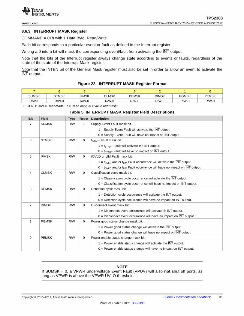
8.6.3 INTERRUPT MASK RegisterCOMMAND = 01h with 1 Data Byte, Read/Write
Each bit corresponds to a particular event or fault as defined in the Interrupt register.
Writing a 0 into a bit will mask the corresponding event/fault from activating the INT output.
Note that the bits of the Interrupt register always change state according to events or faults, regardless of thestate of the state of the Interrupt Mask register.
Note that the INTEN bit of the General Mask register must also be set in order to allow an event to activate theINT output.
Figure 22. INTERRUPT MASK Register Format
7 6 5 4 3 2 1 0SUMSK STMSK IFMSK CLMSK DEMSK DIMSK PGMSK PEMSKR/W-1 R/W-0 R/W-0 R/W-0 R/W-0 R/W-0 R/W-0 R/W-0
LEGEND: R/W = Read/Write; R = Read only; -n = value after reset
Table 5. INTERRUPT MASK Register Field DescriptionsBit Field Type Reset Description7 SUMSK R/W 1 Supply Event Fault mask bit.
1 = Supply Event Fault will activate the INT output.
0 = Supply Event Fault will have no impact on INT output.6 STMSK R/W 0 tSTART Fault mask bit.
1 = tSTART Fault will activate the INT output.
0 = tSTART Fault will have no impact on INT output.5 IFMSK R/W 0 tOVLD or LIM Fault mask bit.
1 = tOVLD and/or tLIM Fault occurrence will activate the INT output
0 = tOVLD and/or tLIM Fault occurrence will have no impact on INT output4 CLMSK R/W 0 Classification cycle mask bit.
1 = Classification cycle occurrence will activate the INT output.
0 = Classification cycle occurrence will have no impact on INT output.3 DEMSK R/W 0 Detection cycle mask bit.
1 = Detection cycle occurrence will activate the INT output.
0 = Detection cycle occurrence will have no impact on INT output.2 DIMSK R/W 0 Disconnect event mask bit.
1 = Disconnect event occurrence will activate th INT output.
0 = Disconnect event occurrence will have no impact on INT output.1 PGMSK R/W 0 Power good status change mask bit.
1 = Power good status change will activate the INT output.
0 = Power good status change will have no impact on INT output.0 PEMSK R/W 0 Power enable status change mask bit.
1 = Power enable status change will activate the INT output.
0 = Power enable status change will have no impact on INT output.
SPACE
NOTEIf SUMSK = 0, a VPWR undervoltage Event Fault (VPUV) will also not shut off ports, aslong as VPWR is above the VPWR UVLO threshold.
32
TPS2388SLUSC25A –FEBRUARY 2015–REVISED AUGUST 2017 www.ti.com
Product Folder Links: TPS2388
Submit Documentation Feedback Copyright © 2015–2017, Texas Instruments Incorporated
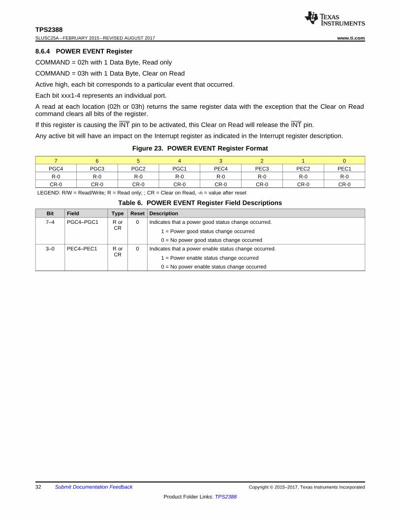
8.6.4 POWER EVENT RegisterCOMMAND = 02h with 1 Data Byte, Read only
COMMAND = 03h with 1 Data Byte, Clear on Read
Active high, each bit corresponds to a particular event that occurred.
Each bit xxx1-4 represents an individual port.
A read at each location (02h or 03h) returns the same register data with the exception that the Clear on Readcommand clears all bits of the register.
If this register is causing the INT pin to be activated, this Clear on Read will release the INT pin.
Any active bit will have an impact on the Interrupt register as indicated in the Interrupt register description.
Figure 23. POWER EVENT Register Format
7 6 5 4 3 2 1 0PGC4 PGC3 PGC2 PGC1 PEC4 PEC3 PEC2 PEC1R-0 R-0 R-0 R-0 R-0 R-0 R-0 R-0
CR-0 CR-0 CR-0 CR-0 CR-0 CR-0 CR-0 CR-0LEGEND: R/W = Read/Write; R = Read only; ; CR = Clear on Read, -n = value after reset
Table 6. POWER EVENT Register Field DescriptionsBit Field Type Reset Description7–4 PGC4–PGC1 R or
CR0 Indicates that a power good status change occurred.
1 = Power good status change occurred
0 = No power good status change occurred3–0 PEC4–PEC1 R or
CR0 Indicates that a power enable status change occurred.
1 = Power enable status change occurred
0 = No power enable status change occurred
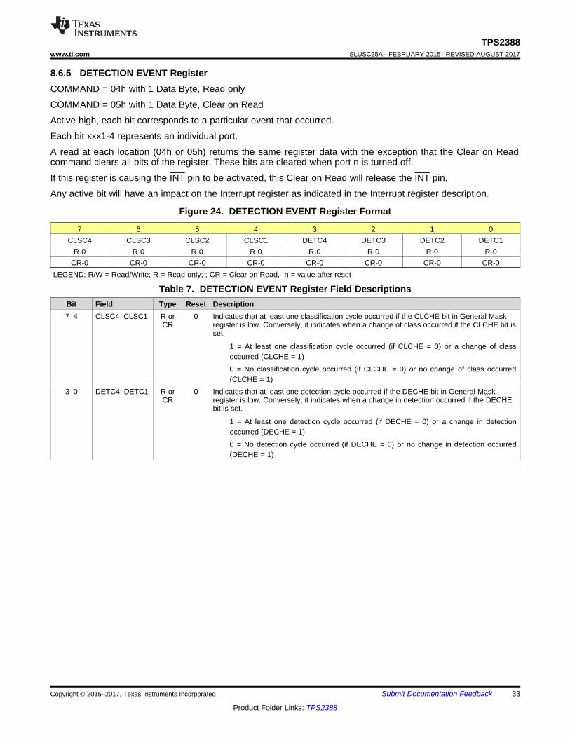
33
TPS2388www.ti.com SLUSC25A –FEBRUARY 2015–REVISED AUGUST 2017
Product Folder Links: TPS2388
Submit Documentation FeedbackCopyright © 2015–2017, Texas Instruments Incorporated
8.6.5 DETECTION EVENT RegisterCOMMAND = 04h with 1 Data Byte, Read only
COMMAND = 05h with 1 Data Byte, Clear on Read
Active high, each bit corresponds to a particular event that occurred.
Each bit xxx1-4 represents an individual port.
A read at each location (04h or 05h) returns the same register data with the exception that the Clear on Readcommand clears all bits of the register. These bits are cleared when port n is turned off.
If this register is causing the INT pin to be activated, this Clear on Read will release the INT pin.
Any active bit will have an impact on the Interrupt register as indicated in the Interrupt register description.
Figure 24. DETECTION EVENT Register Format
7 6 5 4 3 2 1 0CLSC4 CLSC3 CLSC2 CLSC1 DETC4 DETC3 DETC2 DETC1
R-0 R-0 R-0 R-0 R-0 R-0 R-0 R-0CR-0 CR-0 CR-0 CR-0 CR-0 CR-0 CR-0 CR-0
LEGEND: R/W = Read/Write; R = Read only; ; CR = Clear on Read, -n = value after reset
Table 7. DETECTION EVENT Register Field DescriptionsBit Field Type Reset Description7–4 CLSC4–CLSC1 R or
CR0 Indicates that at least one classification cycle occurred if the CLCHE bit in General Mask
register is low. Conversely, it indicates when a change of class occurred if the CLCHE bit isset.
1 = At least one classification cycle occurred (if CLCHE = 0) or a change of classoccurred (CLCHE = 1)
0 = No classification cycle occurred (if CLCHE = 0) or no change of class occurred(CLCHE = 1)
3–0 DETC4–DETC1 R orCR
0 Indicates that at least one detection cycle occurred if the DECHE bit in General Maskregister is low. Conversely, it indicates when a change in detection occurred if the DECHEbit is set.
1 = At least one detection cycle occurred (if DECHE = 0) or a change in detectionoccurred (DECHE = 1)
0 = No detection cycle occurred (if DECHE = 0) or no change in detection occurred(DECHE = 1)

34
TPS2388SLUSC25A –FEBRUARY 2015–REVISED AUGUST 2017 www.ti.com
Product Folder Links: TPS2388
Submit Documentation Feedback Copyright © 2015–2017, Texas Instruments Incorporated
8.6.6 FAULT EVENT RegisterCOMMAND = 06h with 1 Data Byte, Read only
COMMAND = 07h with 1 Data Byte, Clear on Read
Active high, each bit corresponds to a particular event that occurred.
Each bit xxx1-4 represents an individual port.
A read at each location (06h or 07h) returns the same register data with the exception that the Clear on Readcommand clears all bits of the register. These bits are cleared when port n is turned off.
If this register is causing the INT pin to be activated, this Clear on Read will release the INT pin.
Any active bit will have an impact on the Interrupt register as indicated in the Interrupt register description.
Figure 25. FAULT EVENT Register Format
7 6 5 4 3 2 1 0DISF4 DISF3 DISF2 DISF1 ICUT4 ICUT3 ICUT2 ICUT1
R-0 R-0 R-0 R-0 R-0 R-0 R-0 R-0CR-0 CR-0 CR-0 CR-0 CR-0 CR-0 CR-0 CR-0
LEGEND: R/W = Read/Write; R = Read only; ; CR = Clear on Read, -n = value after reset
Table 8. FAULT EVENT Register Field DescriptionsBit Field Type Reset Description7–4 DISF4–DISF1 R or
CR0 Indicates that a disconnect event occurred.
1 = Disconnect event occurred
0 = No disconnect event occurred3–0 ICUT4–ICUT1 R or
CR0 Indicates that a tOVLD Fault occurred.
1 = tOVLD Fault occurred
0 = No tOVLD Fault occurred
Note that if ICUT is disabled for a port, this port will not be automatically turned off during an ICUT faultcondition. However, the ICUT fault flag will still be operational, with a fault timeout equal to tLIM / 2.
Also, if a Clear on Read is done at the Fault Event register, not only the ICUTn bit is reset, but the associatedport ICUT counter is also reset.
Note that this has no impact on TLIM counter at all.
In any other case, ICUT fault is related to TOVLD fault timer as usual and there is no counter reset during clearon read operation.

35
TPS2388www.ti.com SLUSC25A –FEBRUARY 2015–REVISED AUGUST 2017
Product Folder Links: TPS2388
Submit Documentation FeedbackCopyright © 2015–2017, Texas Instruments Incorporated
8.6.7 START/ILIM EVENT RegisterCOMMAND = 08h with 1 Data Byte, Read only
COMMAND = 09h with 1 Data Byte, Clear on Read
Active high, each bit corresponds to a particular event that occurred.
Each bit xxx1-4 represents an individual port.
A read at each location (08h or 09h) returns the same register data with the exception that the Clear on Readcommand clears all bits of the register. These bits are cleared when port n is turned off.
If this register is causing the INT pin to be activated, this Clear on Read will release the INT pin.
Any active bit will have an impact on the Interrupt register as indicated in the Interrupt register description.
Note: When a Start Fault is reported after the IEEE Power Enable command is used, if the PECn bit in PowerEvent register is set, then there is an Inrush fault. If PECn bit is not set, then the Power-On Fault registerindicates the cause of the fault.
Figure 26. START/ILIM EVENT Register Format
7 6 5 4 3 2 1 0ILIM4 ILIM3 ILIM2 ILIM1 STRT4 STRT3 STRT2 STRT1R-0 R-0 R-0 R-0 R-0 R-0 R-0 R-0
CR-0 CR-0 CR-0 CR-0 CR-0 CR-0 CR-0 CR-0LEGEND: R/W = Read/Write; R = Read only; ; CR = Clear on Read, -n = value after reset
Table 9. START/ILIM EVENT Register Field DescriptionsBit Field Type Reset Description7–4 ILIM4–ILIM1 R or
CR0 Indicates that a tLIM fault occurred, which means the port has limited its output current to
ILIM or the folded back ILIM for more than tLIM.
1 = tLIM fault occurred
0 = No tLIM fault occurred3–0 STRT4–STRT1 R or
CR0 Indicates that a tSTART fault occurred at port turn on. Also indicates if a class or detection
error occurred during a port turn on using the IEEE Power Enable command.
1 = tSTART fault or class/detect error occurred
0 = No tSTART fault or class/detect error occurred
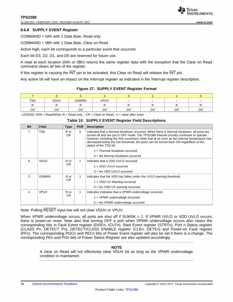
36
TPS2388SLUSC25A –FEBRUARY 2015–REVISED AUGUST 2017 www.ti.com
Product Folder Links: TPS2388
Submit Documentation Feedback Copyright © 2015–2017, Texas Instruments Incorporated
8.6.8 SUPPLY EVENT RegisterCOMMAND = 0Ah with 1 Data Byte, Read only
COMMAND = 0Bh with 1 Data Byte, Clear on Read
Active high, each bit corresponds to a particular event that occurred.
Each bit D3, D2, D1, and D0 are reserved for future use.
A read at each location (0Ah or 0Bh) returns the same register data with the exception that the Clear on Readcommand clears all bits of the register.
If this register is causing the INT pin to be activated, this Clear on Read will release the INT pin.
Any active bit will have an impact on the Interrupt register as indicated in the Interrupt register description.
Figure 27. SUPPLY EVENT Register Format
7 6 5 4 3 2 1 0TSD VDUV VDWRN VPUV – – – –
R R R R R R R RCR CR CR CR CR CR CR CR
LEGEND: R/W = Read/Write; R = Read only; ; CR = Clear on Read, -n = value after reset
Table 10. SUPPLY EVENT Register Field DescriptionsBit Field Type POR Description7 TSD R or
CR0 Indicates that a thermal shutdown occurred. When there is thermal shutdown, all ports are
turned off and are put in OFF mode. The TPS2388 internal circuitry continues to operatehowever, including the A/D converters. Note that at as soon as the internal temperature hasdecreased below the low threshold, the ports can be turned back ON regardless of thestatus of the TSD bit.
1 = Thermal shutdown occurred
0 = No thermal shutdown occurred6 VDUV R or
CR1 Indicates that a VDD UVLO occurred.
1 = VDD UVLO occurred
0 = No VDD UVLO occurred5 VDWRN R or
CR1 Indicates that the VDD has fallen under the UVLO warning threshold.
1 = VDD UV Warning occurred
0 = No VDD UV warning occurred4 VPUV R or
CR1 Indicates Indicates that a VPWR undervoltage occurred.
1 = VPWR undervoltage occurred
0 = No VPWR undervoltage occurred
Note: Pulling RESET input low will not clear VDUV or VPUV.
When VPWR undervoltage occurs, all ports are shut off if SUMSK = 1. If VPWR UVLO or VDD UVLO occurs,there is power-on reset. Note also that turning OFF a port when VPWR undervoltage occurs also clears thecorresponding bits in Fault Event register (DISFn, ICUTn), Start Event register (STRTn), Port n Status register(CLASS Pn, DETECT Pn), DETECT/CLASS ENABLE register (CLEn, DETEn) and Power-on Fault register(PFn). The corresponding PGCn and PECn bits of Power Event register will also be set if there is a change. Thecorresponding PEn and PGn bits of Power Status Register are also updated accordingly.
NOTEA clear on Read will not effectively clear VDUV bit as long as the VPWR undervoltagecondition is maintained.
37
TPS2388www.ti.com SLUSC25A –FEBRUARY 2015–REVISED AUGUST 2017
Product Folder Links: TPS2388
Submit Documentation FeedbackCopyright © 2015–2017, Texas Instruments Incorporated
NOTEIf SUMSK = 0, a VPWR undervoltage Event Fault (VPUV) will not shut off ports, as longas VPWR is above the VPWR UVLO threshold.
NOTEDuring VPWR undervoltage, the Detection Event register (CLSCn, DETCn) is not cleared,unless VPWR also falls below the VPWR UVLO falling threshold.
NOTEIf VPWR UVLO or VDD UVLO occurs, the I2C interface stops operating, and SDAO isforced low.
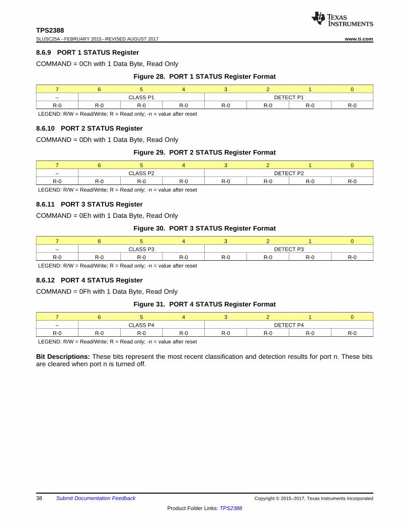
38
TPS2388SLUSC25A –FEBRUARY 2015–REVISED AUGUST 2017 www.ti.com
Product Folder Links: TPS2388
Submit Documentation Feedback Copyright © 2015–2017, Texas Instruments Incorporated
8.6.9 PORT 1 STATUS RegisterCOMMAND = 0Ch with 1 Data Byte, Read Only
Figure 28. PORT 1 STATUS Register Format
7 6 5 4 3 2 1 0– CLASS P1 DETECT P1
R-0 R-0 R-0 R-0 R-0 R-0 R-0 R-0LEGEND: R/W = Read/Write; R = Read only; -n = value after reset
8.6.10 PORT 2 STATUS RegisterCOMMAND = 0Dh with 1 Data Byte, Read Only
Figure 29. PORT 2 STATUS Register Format
7 6 5 4 3 2 1 0– CLASS P2 DETECT P2
R-0 R-0 R-0 R-0 R-0 R-0 R-0 R-0LEGEND: R/W = Read/Write; R = Read only; -n = value after reset
8.6.11 PORT 3 STATUS RegisterCOMMAND = 0Eh with 1 Data Byte, Read Only
Figure 30. PORT 3 STATUS Register Format
7 6 5 4 3 2 1 0– CLASS P3 DETECT P3
R-0 R-0 R-0 R-0 R-0 R-0 R-0 R-0LEGEND: R/W = Read/Write; R = Read only; -n = value after reset
8.6.12 PORT 4 STATUS RegisterCOMMAND = 0Fh with 1 Data Byte, Read Only
Figure 31. PORT 4 STATUS Register Format
7 6 5 4 3 2 1 0– CLASS P4 DETECT P4
R-0 R-0 R-0 R-0 R-0 R-0 R-0 R-0LEGEND: R/W = Read/Write; R = Read only; -n = value after reset
Bit Descriptions: These bits represent the most recent classification and detection results for port n. These bitsare cleared when port n is turned off.
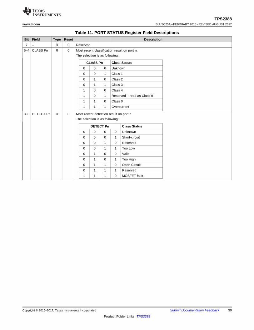
39
TPS2388www.ti.com SLUSC25A –FEBRUARY 2015–REVISED AUGUST 2017
Product Folder Links: TPS2388
Submit Documentation FeedbackCopyright © 2015–2017, Texas Instruments Incorporated
Table 11. PORT STATUS Register Field DescriptionsBit Field Type Reset Description7 – R 0 Reserved
6–4 CLASS Pn R 0 Most recent classification result on port n.The selection is as following:
CLASS Pn Class Status0 0 0 Unknown0 0 1 Class 10 1 0 Class 20 1 1 Class 31 0 0 Class 41 0 1 Reserved – read as Class 01 1 0 Class 01 1 1 Overcurrent
3–0 DETECT Pn R 0 Most recent detection result on port n.The selection is as following:
DETECT Pn Class Status0 0 0 0 Unknown0 0 0 1 Short-circuit0 0 1 0 Reserved0 0 1 1 Too Low0 1 0 0 Valid0 1 0 1 Too High0 1 1 0 Open Circuit0 1 1 1 Reserved1 1 1 0 MOSFET fault

40
TPS2388SLUSC25A –FEBRUARY 2015–REVISED AUGUST 2017 www.ti.com
Product Folder Links: TPS2388
Submit Documentation Feedback Copyright © 2015–2017, Texas Instruments Incorporated
8.6.13 POWER STATUS RegisterCOMMAND = 10h with 1 Data Byte, Read only
Each bit represents the actual power status of a port.
Each bit xx1-4 represents an individual port..
These bits are cleared when port n is turned off, including if the turn off is caused by a fault condition.
Figure 32. POWER STATUS Register Format
7 6 5 4 3 2 1 0PG4 PG3 PG2 PG1 PE4 PE3 PE2 PE1R-0 R-0 R-0 R-0 R-0 R-0 R-0 R-0
LEGEND: R/W = Read/Write; R = Read only; -n = value after reset
Table 12. POWER STATUS Register Field DescriptionsBit Field Type Reset Description7–4 PG4–PG1 R 0 Each bit, when at 1, indicates that the port is on and that the voltage at DRAINn pin has
gone below the power good threshold during the port turn on.These bits are latched high once the turn on is complete and can only be cleared when theport is turned off or at RESET/POR.
1 = Power is good
0 = Power is not good3–0 PE4–PE1 R 0 Each bit indicates the ON/OFF state of the corresponding port.
1 = Port is on
0 = Port is off
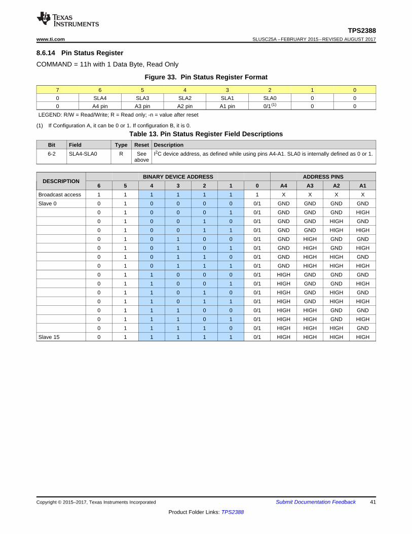
41
TPS2388www.ti.com SLUSC25A –FEBRUARY 2015–REVISED AUGUST 2017
Product Folder Links: TPS2388
Submit Documentation FeedbackCopyright © 2015–2017, Texas Instruments Incorporated
8.6.14 Pin Status RegisterCOMMAND = 11h with 1 Data Byte, Read Only
(1) If Configuration A, it can be 0 or 1. If configuration B, it is 0.
Figure 33. Pin Status Register Format
7 6 5 4 3 2 1 00 SLA4 SLA3 SLA2 SLA1 SLA0 0 00 A4 pin A3 pin A2 pin A1 pin 0/1 (1) 0 0
LEGEND: R/W = Read/Write; R = Read only; -n = value after reset
Table 13. Pin Status Register Field DescriptionsBit Field Type Reset Description6-2 SLA4-SLA0 R See
aboveI2C device address, as defined while using pins A4-A1. SLA0 is internally defined as 0 or 1.
DESCRIPTIONBINARY DEVICE ADDRESS ADDRESS PINS
6 5 4 3 2 1 0 A4 A3 A2 A1Broadcast access 1 1 1 1 1 1 1 X X X XSlave 0 0 1 0 0 0 0 0/1 GND GND GND GND
0 1 0 0 0 1 0/1 GND GND GND HIGH0 1 0 0 1 0 0/1 GND GND HIGH GND0 1 0 0 1 1 0/1 GND GND HIGH HIGH0 1 0 1 0 0 0/1 GND HIGH GND GND0 1 0 1 0 1 0/1 GND HIGH GND HIGH0 1 0 1 1 0 0/1 GND HIGH HIGH GND0 1 0 1 1 1 0/1 GND HIGH HIGH HIGH0 1 1 0 0 0 0/1 HIGH GND GND GND0 1 1 0 0 1 0/1 HIGH GND GND HIGH0 1 1 0 1 0 0/1 HIGH GND HIGH GND0 1 1 0 1 1 0/1 HIGH GND HIGH HIGH0 1 1 1 0 0 0/1 HIGH HIGH GND GND0 1 1 1 0 1 0/1 HIGH HIGH GND HIGH0 1 1 1 1 0 0/1 HIGH HIGH HIGH GND
Slave 15 0 1 1 1 1 1 0/1 HIGH HIGH HIGH HIGH
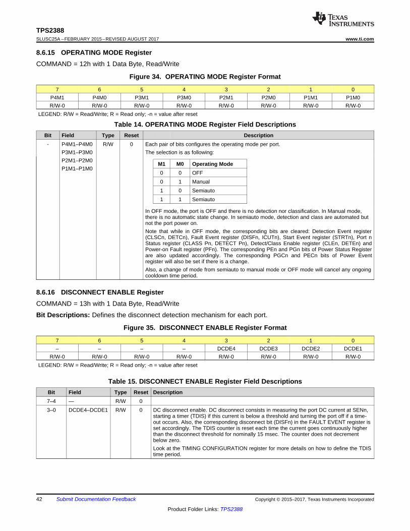
42
TPS2388SLUSC25A –FEBRUARY 2015–REVISED AUGUST 2017 www.ti.com
Product Folder Links: TPS2388
Submit Documentation Feedback Copyright © 2015–2017, Texas Instruments Incorporated
8.6.15 OPERATING MODE RegisterCOMMAND = 12h with 1 Data Byte, Read/Write
Figure 34. OPERATING MODE Register Format
7 6 5 4 3 2 1 0P4M1 P4M0 P3M1 P3M0 P2M1 P2M0 P1M1 P1M0R/W-0 R/W-0 R/W-0 R/W-0 R/W-0 R/W-0 R/W-0 R/W-0
LEGEND: R/W = Read/Write; R = Read only; -n = value after reset
Table 14. OPERATING MODE Register Field DescriptionsBit Field Type Reset Description- P4M1–P4M0
P3M1–P3M0P2M1–P2M0P1M1–P1M0
R/W 0 Each pair of bits configures the operating mode per port.The selection is as following:
M1 M0 Operating Mode0 0 OFF0 1 Manual1 0 Semiauto1 1 Semiauto
In OFF mode, the port is OFF and there is no detection nor classification. In Manual mode,there is no automatic state change. In semiauto mode, detection and class are automated butnot the port power on.Note that while in OFF mode, the corresponding bits are cleared: Detection Event register(CLSCn, DETCn), Fault Event register (DISFn, ICUTn), Start Event register (STRTn), Port nStatus register (CLASS Pn, DETECT Pn), Detect/Class Enable register (CLEn, DETEn) andPower-on Fault register (PFn). The corresponding PEn and PGn bits of Power Status Registerare also updated accordingly. The corresponding PGCn and PECn bits of Power Eventregister will also be set if there is a change.Also, a change of mode from semiauto to manual mode or OFF mode will cancel any ongoingcooldown time period.
8.6.16 DISCONNECT ENABLE RegisterCOMMAND = 13h with 1 Data Byte, Read/Write
Bit Descriptions: Defines the disconnect detection mechanism for each port.
Figure 35. DISCONNECT ENABLE Register Format
7 6 5 4 3 2 1 0– – – – DCDE4 DCDE3 DCDE2 DCDE1
R/W-0 R/W-0 R/W-0 R/W-0 R/W-0 R/W-0 R/W-0 R/W-0LEGEND: R/W = Read/Write; R = Read only; -n = value after reset
Table 15. DISCONNECT ENABLE Register Field DescriptionsBit Field Type Reset Description7–4 — R/W 03–0 DCDE4–DCDE1 R/W 0 DC disconnect enable. DC disconnect consists in measuring the port DC current at SENn,
starting a timer (TDIS) if this current is below a threshold and turning the port off if a time-out occurs. Also, the corresponding disconnect bit (DISFn) in the FAULT EVENT register isset accordingly. The TDIS counter is reset each time the current goes continuously higherthan the disconnect threshold for nominally 15 msec. The counter does not decrementbelow zero.Look at the TIMING CONFIGURATION register for more details on how to define the TDIStime period.
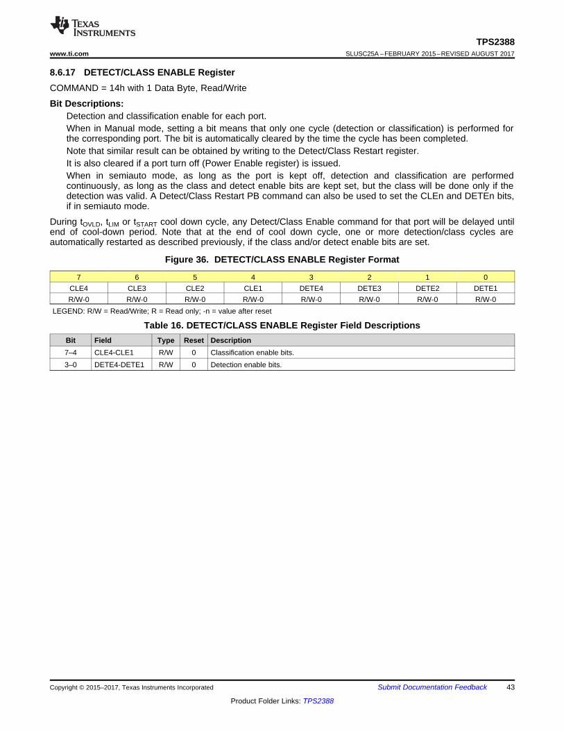
43
TPS2388www.ti.com SLUSC25A –FEBRUARY 2015–REVISED AUGUST 2017
Product Folder Links: TPS2388
Submit Documentation FeedbackCopyright © 2015–2017, Texas Instruments Incorporated
8.6.17 DETECT/CLASS ENABLE RegisterCOMMAND = 14h with 1 Data Byte, Read/Write
Bit Descriptions:Detection and classification enable for each port.When in Manual mode, setting a bit means that only one cycle (detection or classification) is performed forthe corresponding port. The bit is automatically cleared by the time the cycle has been completed.Note that similar result can be obtained by writing to the Detect/Class Restart register.It is also cleared if a port turn off (Power Enable register) is issued.When in semiauto mode, as long as the port is kept off, detection and classification are performedcontinuously, as long as the class and detect enable bits are kept set, but the class will be done only if thedetection was valid. A Detect/Class Restart PB command can also be used to set the CLEn and DETEn bits,if in semiauto mode.
During tOVLD, tLIM or tSTART cool down cycle, any Detect/Class Enable command for that port will be delayed untilend of cool-down period. Note that at the end of cool down cycle, one or more detection/class cycles areautomatically restarted as described previously, if the class and/or detect enable bits are set.
Figure 36. DETECT/CLASS ENABLE Register Format
7 6 5 4 3 2 1 0CLE4 CLE3 CLE2 CLE1 DETE4 DETE3 DETE2 DETE1R/W-0 R/W-0 R/W-0 R/W-0 R/W-0 R/W-0 R/W-0 R/W-0
LEGEND: R/W = Read/Write; R = Read only; -n = value after reset
Table 16. DETECT/CLASS ENABLE Register Field DescriptionsBit Field Type Reset Description7–4 CLE4-CLE1 R/W 0 Classification enable bits.3–0 DETE4-DETE1 R/W 0 Detection enable bits.
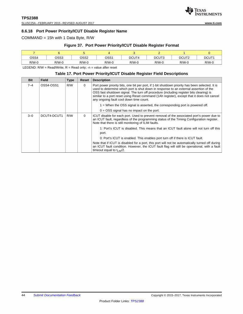
44
TPS2388SLUSC25A –FEBRUARY 2015–REVISED AUGUST 2017 www.ti.com
Product Folder Links: TPS2388
Submit Documentation Feedback Copyright © 2015–2017, Texas Instruments Incorporated
8.6.18 Port Power Priority/ICUT Disable Register NameCOMMAND = 15h with 1 Data Byte, R/W
Figure 37. Port Power Priority/ICUT Disable Register Format
7 6 5 4 3 2 1 0OSS4 OSS3 OSS2 OSS1 DCUT4 DCUT3 DCUT2 DCUT1R/W-0 R/W-0 R/W-0 R/W-0 R/W-0 R/W-0 R/W-0 R/W-0
LEGEND: R/W = Read/Write; R = Read only; -n = value after reset
Table 17. Port Power Priority/ICUT Disable Register Field DescriptionsBit Field Type Reset Description7–4 OSS4-OSS1 R/W 0 Port power priority bits, one bit per port, if 1-bit shutdown priority has been selected. It is
used to determine which port is shut down in response to an external assertion of theOSS fast shutdown signal. The turn off procedure (including register bits clearing) issimilar to a port reset using Reset command (1Ah register), except that it does not cancelany ongoing fault cool down time count.
1 = When the OSS signal is asserted, the corresponding port is powered off.
0 = OSS signal has no impact on the port.3–0 DCUT4-DCUT1 R/W 0 ICUT disable for each port. Used to prevent removal of the associated port’s power due to
an ICUT fault, regardless of the programming status of the Timing Configuration register.Note that there is still monitoring of ILIM faults.
1: Port’s ICUT is disabled. This means that an ICUT fault alone will not turn off thisport.
0: Port’s ICUT is enabled. This enables port turn off if there is ICUT fault.Note that if ICUT is disabled for a port, this port will not be automatically turned off duringan ICUT fault condition. However, the ICUT fault flag will still be operational, with a faulttimeout equal to tLIM/2.
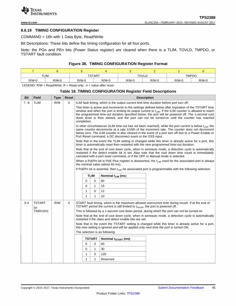
45
TPS2388www.ti.com SLUSC25A –FEBRUARY 2015–REVISED AUGUST 2017
Product Folder Links: TPS2388
Submit Documentation FeedbackCopyright © 2015–2017, Texas Instruments Incorporated
8.6.19 TIMING CONFIGURATION RegisterCOMMAND = 16h with 1 Data Byte, Read/Write
Bit Descriptions: These bits define the timing configuration for all four ports.
Note: the PGn and PEn bits (Power Status register) are cleared when there is a TLIM, TOVLD, TMPDO, orTSTART fault condition.
Figure 38. TIMING CONFIGURATION Register Format
7 6 5 4 3 2 1 0TLIM TSTART TOVLD TMPDO
R/W-0 R/W-0 R/W-0 R/W-0 R/W-0 R/W-0 R/W-0 R/W-0LEGEND: R/W = Read/Write; R = Read only; -n = value after reset
Table 18. TIMING CONFIGURATION Register Field DescriptionsBit Field Type Reset Description
7 –6 TLIM R/W 0 ILIM fault timing, which is the output current limit time duration before port turn off.This timer is active and increments to the settings defined below after expiration of the TSTART timewindow and when the port is limiting its output current to ILIM. If the ILIM counter is allowed to reachthe programmed time-out duration specified below, the port will be powered off. The 1-second cooldown timer is then started, and the port can not be turned-on until the counter has reachedcompletion.In other circumstances (ILIM time-out has not been reached), while the port current is below ILIM, thesame counter decrements at a rate 1/16th of the increment rate. The counter does not decrementbelow zero. The ILIM counter is also cleared in the event of a port turn off due to a Power Enable orPort Reset command, a DC disconnect event or the OSS input.Note that in the event the TLIM setting is changed while this timer is already active for a port, thistimer is automatically reset then restarted with the new programmed time-out duration.Note that at the end of cool down cycle, when in semiauto mode, a detection cycle is automaticallyrestarted if the detect enable bit is set. Also note that the cool down time count is immediatelycanceled with a port reset command, or if the OFF or Manual mode is selected.When a PoEPn bit in PoE Plus register is deasserted, the tLIM used for the associated port is alwaysthe nominal value (about 60 ms).If PoEPn bit is asserted, then tLIM for associated port is programmable with the following selection:
TLIM Nominal tLIM (ms)0 0 600 1 151 0 121 1 10
5-4 TSTART(orTINRUSH)
R/W 0 START fault timing, which is the maximum allowed overcurrent time during inrush. If at the end ofTSTART period the current is still limited to IInrush, the port is powered off.This is followed by a 1-second cool down period, during which the port can not be turned-onNote that at the end of cool down cycle, when in semiauto mode, a detection cycle is automaticallyrestarted if the class and detect enable bits are set.Note that in the event the TSTART setting is changed while this timer is already active for a port,this new setting is ignored and will be applied only next time the port is turned ON.The selection is as following:
TSTART Nominal tSTART (ms)0 0 600 1 301 0 1201 1 Reserved
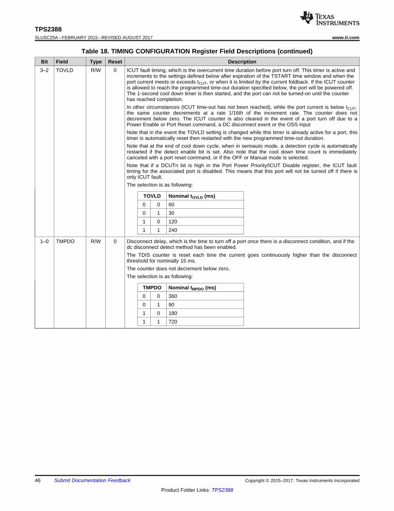
46
TPS2388SLUSC25A –FEBRUARY 2015–REVISED AUGUST 2017 www.ti.com
Product Folder Links: TPS2388
Submit Documentation Feedback Copyright © 2015–2017, Texas Instruments Incorporated
Table 18. TIMING CONFIGURATION Register Field Descriptions (continued)Bit Field Type Reset Description3–2 TOVLD R/W 0 ICUT fault timing, which is the overcurrent time duration before port turn off. This timer is active and
increments to the settings defined below after expiration of the TSTART time window and when theport current meets or exceeds ICUT, or when it is limited by the current foldback. If the ICUT counteris allowed to reach the programmed time-out duration specified below, the port will be powered off.The 1-second cool down timer is then started, and the port can not be turned-on until the counterhas reached completion.In other circumstances (ICUT time-out has not been reached), while the port current is below ICUT,the same counter decrements at a rate 1/16th of the increment rate. The counter does notdecrement below zero. The ICUT counter is also cleared in the event of a port turn off due to aPower Enable or Port Reset command, a DC disconnect event or the OSS inputNote that in the event the TOVLD setting is changed while this timer is already active for a port, thistimer is automatically reset then restarted with the new programmed time-out duration.Note that at the end of cool down cycle, when in semiauto mode, a detection cycle is automaticallyrestarted if the detect enable bit is set. Also note that the cool down time count is immediatelycanceled with a port reset command, or if the OFF or Manual mode is selected.Note that if a DCUTn bit is high in the Port Power Priority/ICUT Disable register, the ICUT faulttiming for the associated port is disabled. This means that this port will not be turned off if there isonly ICUT fault.The selection is as following:
TOVLD Nominal tOVLD (ms)0 0 600 1 301 0 1201 1 240
1–0 TMPDO R/W 0 Disconnect delay, which is the time to turn off a port once there is a disconnect condition, and if thedc disconnect detect method has been enabled.The TDIS counter is reset each time the current goes continuously higher than the disconnectthreshold for nominally 15 ms.The counter does not decrement below zero.The selection is as following:
TMPDO Nominal tMPDO (ms)0 0 3600 1 901 0 1801 1 720

47
TPS2388www.ti.com SLUSC25A –FEBRUARY 2015–REVISED AUGUST 2017
Product Folder Links: TPS2388
Submit Documentation FeedbackCopyright © 2015–2017, Texas Instruments Incorporated
8.6.20 GENERAL MASK RegisterCOMMAND = 17h with 1 Data Byte, Read/Write
Figure 39. GENERAL MASK Register Format
7 6 5 4 3 2 1 0INTEN – nbitACC MbitPrty CLCHE DECHE – –R/W-1 R/W-0 R/W-0 R/W-0 R/W-0 R/W-0 R/W-0 R/W-0
LEGEND: R/W = Read/Write; R = Read only; -n = value after reset
Table 19. GENERAL MASK Register Field DescriptionsBit Field Type Reset Description7 INTEN R/W 1 INT pin mask bit. Writing a 0 will mask any bit of Interrupt register from activating the INT
output, whatever the state of the Interrupt Mask register. Note that activating INTEN has noimpact on the event registers.
1 = Any unmasked bit of Interrupt register can activate the INT output
0 = INT output cannot be activated6 – R/W 05 nbitACC R/W 0 Register Access Configuration bit. Used to select configuration A or B.
1 = Configuration B. This means 16-bit access with a single device address.
0 = Configuration A. This means 8-bit access, while the 8-port device is treated as 2separate 4-port devices with 2 consecutive slave addresses.
4 MbitPrty R/W 0 Multi Bit Priority bit. Used to select between 1-bit shutdown priority and 3-bit shutdownpriority.
1 = 3-bit shutdown priority. Register 0x27 and 0x28 need to be followed for portpriority and OSS action.
0 = 1-bit shutdown priority. Register 0x15 needs to be followed for port priority andOSS action
Note: If the MbitPrty bit needs to be changed from 0 to 1, make sure the OSS input is in theidle (low) state for a minimum of 200 µsec prior to setting the MbitPrty bit, to avoid any portmisbehavior related to loss of synchronization with the OSS bit stream.
3 CLCHE R/W 0 Class change Enable bit. When set, the CLSCn bits in Detection Event register onlyindicates when the result of the most current classification operation differs from the resultof the previous one.
1 = CLSCn bit is set only when a change of class occurred for the associated port.
0 = CLSCn bit is set each time a classification cycle occurred for the associated port.2 DECHE R/W 0 Detect Change Enable bit. When set, the DETCn bits in Detection Event register only
indicates when the result of the most current detection operation differs from the result ofthe previous one.
1 = DETCn bit is set only when a change in detection occurred for the associated port.
0 = DETCn bit is set each time a detection cycle occurred for the associated port.1 – R/W 00 – R/W 0

48
TPS2388SLUSC25A –FEBRUARY 2015–REVISED AUGUST 2017 www.ti.com
Product Folder Links: TPS2388
Submit Documentation Feedback Copyright © 2015–2017, Texas Instruments Incorporated
8.6.21 DETECT/CLASS RESTART RegisterCOMMAND = 18h with 1 Data Byte, Write Only
Push button register.
Each bit corresponds to a particular cycle (detect or class restart) per port. Each cycle can be individuallytriggered by writing a 1 at that bit location, while writing a 0 does not change anything for that event.
In Manual mode, a single cycle (detect or class restart) will be triggered while in Semiauto mode, it sets thecorresponding bit in the Detect/Class Enable register.
A Read operation will return 00h.
During tOVLD, tLIM or tSTART cool down cycle, any Detect/Class Restart command for that port will be accepted butthe corresponding action will be delayed until end of cool-down period.
Figure 40. DETECT/CLASS RESTART Register Format
7 6 5 4 3 2 1 0RCL4 RCL3 RCL2 RCL1 RDET4 RDET3 RDET2 RDET1W-0 W-0 W-0 W-0 W-0 W-0 W-0 W-0
LEGEND: R/W = Read/Write; R = Read only; W = Write only; -n = value after reset
Table 20. DETECT/CLASS RESTART Register Field DescriptionsBit Field Type Reset Description7–4 RCL4–RCL1 W 0 Restart classification bit3–0 RDET4–RDET1 W 0 Restart detection bits

49
TPS2388www.ti.com SLUSC25A –FEBRUARY 2015–REVISED AUGUST 2017
Product Folder Links: TPS2388
Submit Documentation FeedbackCopyright © 2015–2017, Texas Instruments Incorporated
8.6.22 POWER ENABLE RegisterCOMMAND = 19h with 1 Data Byte, Write Only
Push button register.
Used to force a port(s) turn on or turn off in any mode except OFF mode. If TPON bit in the PoE Plus register islow, or if the PSE controller is configured in Manual mode, writing a 1 at that PWONn bit location will immediatelyturn on the associated port, regardless of the classification and detection status and regardless of the IEEE802.3TPON timing specification. This is also the case if TPON is set and DETn bit is 0, in semiauto mode.
If TPON bit in the PoE Plus register is set, and DETn bit (DETECT/CLASS ENABLE register) is set and while insemiauto mode, writing a 1 at a PWONn bit will turn on the associated port but only if the IEEE802.3 TPONtiming specification can be met and if the detection is valid (and class is valid if enabled). TPON specification isthe time from the completion of a valid detection cycle to port turn ON.
If TPON specification cannot be met, a new detection cycle is restarted, followed by a classification cycle ifenabled, at the end of which the port is turned on, but only if a valid detection is returned and the IEEE802.3TPON specification can be met. For this case, there is no additional attempt to turn on the port until this pushbutton is reasserted. If the last detection result is not valid, the port is not turned on.
Note that in semiauto, as long as the port is kept off, detection and classification are performed continuously, ifthe corresponding class and detect enable bits are set.
Writing a 1 at POFFn location turns off the associated port.
Note that writing a 1 at POFFn and PWONn of same port during the same write operation turns the port off.
Also note that tOVLD, tLIM, tSTART, and disconnect events have priority over the power on command. During tOVLD,tLIM, or tSTART cool down cycle, any port turn on using Power Enable command will be ignored and the port will bekept off.
Turning OFF a port with this command also clears the corresponding bits in Detection Event register (CLSCn,DETCn), Fault Event register (DISFn, ICUTn), Start Event register (STRTn, ILIMn), Port n Status register(CLASS Pn, DETECT Pn), DETECT/CLASS ENABLE register (CLEn, DETEn) and Power-on Fault register(PFn). The corresponding PGCn and PECn bits of Power Event register will also be set if there is a change. Thecorresponding PEn and PGn bits of Power Status Register are also updated accordingly.
Figure 41. POWER ENABLE Register Format
7 6 5 4 3 2 1 0POFF4 POFF3 POFF2 POFF1 PWON4 PWON3 PWON2 PWON1
W-0 W-0 W-0 W-0 W-0 W-0 W-0 W-0LEGEND: R/W = Read/Write; R = Read only; W = Write only; -n = value after reset
Table 21. POWER ENABLE Register Field DescriptionsBit Field Type Reset Description7–4 POFF4–POFF1 W 0 Port power off bits3–0 PWON4–PWON1 W 0 Port power on bits

50
TPS2388SLUSC25A –FEBRUARY 2015–REVISED AUGUST 2017 www.ti.com
Product Folder Links: TPS2388
Submit Documentation Feedback Copyright © 2015–2017, Texas Instruments Incorporated
8.6.23 RESET RegisterCOMMAND = 1Ah with 1 Data Byte, Write Only
Push button register.
Writing a 1 at a bit location triggers an event while a 0 has no impact. Self-clearing bits.
Figure 42. RESET Register Format
7 6 5 4 3 2 1 0CLRAIN CLINP – RESAL RESP4 RESP3 RESP2 RESP1
W-0 W-0 W-0 W-0 W-0 W-0 W-0 W-0LEGEND: R/W = Read/Write; R = Read only; W = Write only; -n = value after reset
Table 22. RESET Register Field DescriptionsBit Field Type Reset Description7 CLRAIN W 0 Clear all interrupts bit. Writing a 1 to CLRAIN clears all event registers and all bits in the
Interrupt register. It also releases the INT pin6 CLINP W 0 When set, it releases the INT pin without any impact on the Event registers nor on the
Interrupt register.5 – W 04 RESAL W 0 Reset all bits when RESAL is set. Results in a state equivalent to a power-up reset. Note
that the VDUV and VPUV bits (Supply Event register) follow the state of VDD and VPWRsupply rails.
3–0 RESP4–RESP1 W 0 Reset port bits. Used to force an immediate port(s) turn off in any mode, by writing a 1 atthe corresponding RESPn bit location(s).Turning OFF a port with this command also clears the corresponding bits in DetectionEvent register (CLSCn, DETCn), Fault Event register (DISFn, ICUTn), Start Event register(STRTn, ILIMn), Port n Status register (CLASS Pn, DETECT Pn), DETECT/CLASSENABLE register (CLEn, DETEn) and Power-on Fault register (PFn). Note that the port canbe turned back on immediately after a port reset; this means that any ongoing cool downcycle becomes immediately terminated once a port reset is received.The corresponding PGCn and PECn bits of Power Event register will also be set if there isa change. The corresponding PEn and PGn bits of Power Status Register are also updatedaccordingly.
8.6.24 ID RegisterCOMMAND = 1Bh with 1 Data Byte, Read/Write
Figure 43. ID Register Format
7 6 5 4 3 2 1 0MFR ID ICV
R/W-0 R/W-1 R/W-0 R/W-1 R/W-0 R/W-0 R/W-1 R/W-1LEGEND: R/W = Read/Write; R = Read only; -n = value after reset
Table 23. ID Register Field DescriptionsBit Field Type Reset Description7–3 MFR ID R/W 01010
bManufacture Identification number (0101,0)
2–0 ICV R/W 011b IC version number (011)

51
TPS2388www.ti.com SLUSC25A –FEBRUARY 2015–REVISED AUGUST 2017
Product Folder Links: TPS2388
Submit Documentation FeedbackCopyright © 2015–2017, Texas Instruments Incorporated
8.6.25 Police 21 Configuration RegisterCOMMAND = 1Eh with 1 Data Byte, Read/Write
Replaces the ICUT mechanism. The threshold is defined with the Police bits and the PoE Plus register.
Figure 44. Police 21 Register Format
7 6 5 4 3 2 1 0POL2_3 POL2_2 POL2_1 POL2_0 POL1_3 POL1_2 POL1_1 POL1_0R/W-1 R/W-1 R/W-1 R/W-1 R/W-1 R/W-1 R/W-1 R/W1
LEGEND: R/W = Read/Write; R = Read only; -n = value after reset
8.6.26 Police 43 Configuration RegisterCOMMAND = 1Fh with 1 Data Byte, Read/Write
Replaces the ICUT mechanism. The threshold is defined with the Police bits and the PoE Plus register.
Figure 45. Police 43 Register Format
7 6 5 4 3 2 1 0POL4_3 POL4_2 POL4_1 POL4_0 POL3_3 POL3_2 POL3_1 POL3_0R/W-1 R/W-1 R/W-1 R/W-1 R/W-1 R/W-1 R/W-1 R/W1
LEGEND: R/W = Read/Write; R = Read only; -n = value after reset
Table 24. Police 43 Register Field DescriptionsBit Field Type Reset Description7–0 POLn_3-
POLn_0R/W 1 4-bit nibble defining ICUT threshold. The result varies depending on the PoE Plus port bit.
The equation defining the ICUT threshold is:
ICUT = (N × ICSTEP) + ICOFFS
Where, when assuming 0.255-Ω Rsense resistor is used:
ICSTEP = 20 mA (1 W resolution if at 50 V) when the associated port’s PoE Plus bit is 0
ICSTEP = 40 mA (2 W resolution if at 50 V)when the associated port’s PoE Plus bit is 1and:
ICOFFS = 20 mA when the associated port’s PoE Plus bit is 0
ICOFFS = 320 mA (16 W if at 50 V) when the associated port’s PoE Plus bit is 1Note:
When a PoEPn bit is set in PoE Plus register, the corresponding POLn bits are initiallychanged to 0x0.
When a PoEPn bit is reset in PoE Plus register, the corresponding POLn bits are initiallychanged to 0xF.
In both cases, the port police current threshold is the same value.
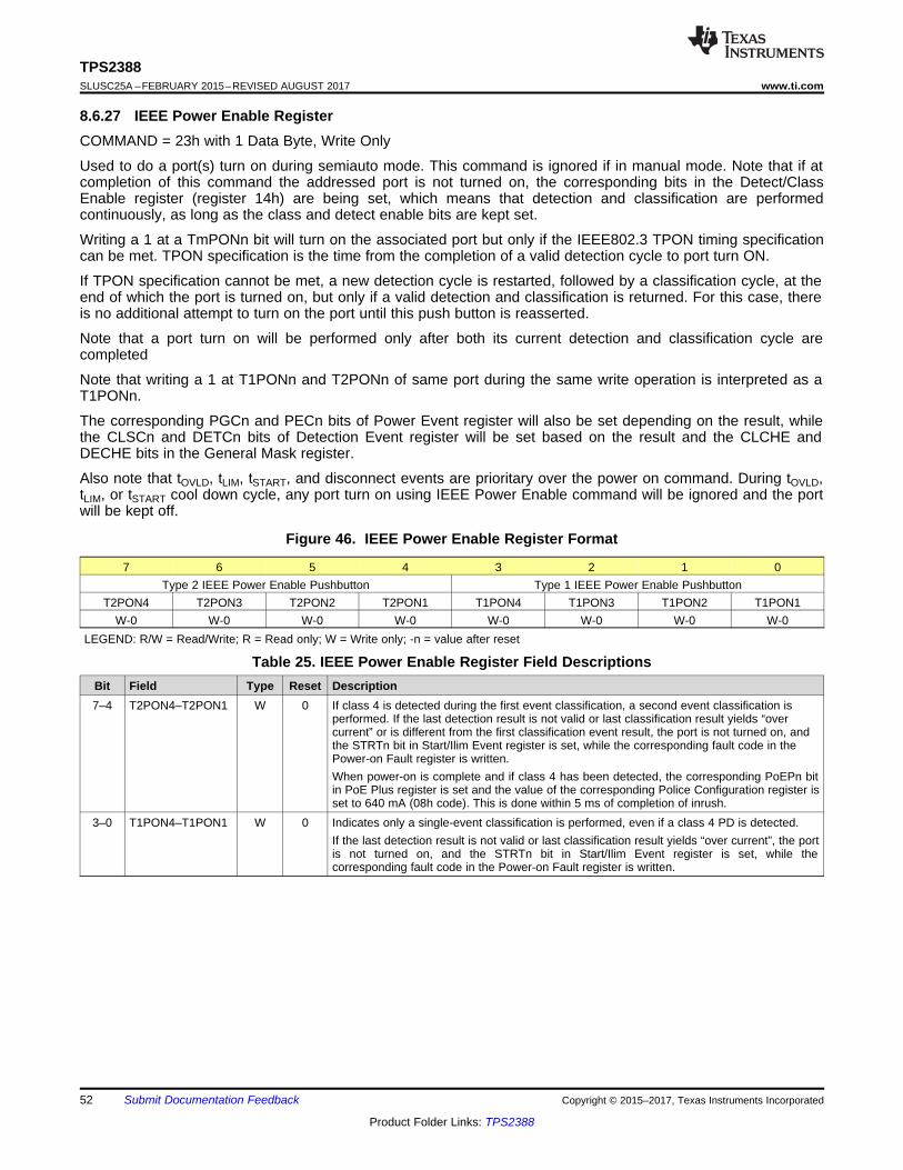
52
TPS2388SLUSC25A –FEBRUARY 2015–REVISED AUGUST 2017 www.ti.com
Product Folder Links: TPS2388
Submit Documentation Feedback Copyright © 2015–2017, Texas Instruments Incorporated
8.6.27 IEEE Power Enable RegisterCOMMAND = 23h with 1 Data Byte, Write Only
Used to do a port(s) turn on during semiauto mode. This command is ignored if in manual mode. Note that if atcompletion of this command the addressed port is not turned on, the corresponding bits in the Detect/ClassEnable register (register 14h) are being set, which means that detection and classification are performedcontinuously, as long as the class and detect enable bits are kept set.
Writing a 1 at a TmPONn bit will turn on the associated port but only if the IEEE802.3 TPON timing specificationcan be met. TPON specification is the time from the completion of a valid detection cycle to port turn ON.
If TPON specification cannot be met, a new detection cycle is restarted, followed by a classification cycle, at theend of which the port is turned on, but only if a valid detection and classification is returned. For this case, thereis no additional attempt to turn on the port until this push button is reasserted.
Note that a port turn on will be performed only after both its current detection and classification cycle arecompleted
Note that writing a 1 at T1PONn and T2PONn of same port during the same write operation is interpreted as aT1PONn.
The corresponding PGCn and PECn bits of Power Event register will also be set depending on the result, whilethe CLSCn and DETCn bits of Detection Event register will be set based on the result and the CLCHE andDECHE bits in the General Mask register.
Also note that tOVLD, tLIM, tSTART, and disconnect events are prioritary over the power on command. During tOVLD,tLIM, or tSTART cool down cycle, any port turn on using IEEE Power Enable command will be ignored and the portwill be kept off.
Figure 46. IEEE Power Enable Register Format
7 6 5 4 3 2 1 0Type 2 IEEE Power Enable Pushbutton Type 1 IEEE Power Enable Pushbutton
T2PON4 T2PON3 T2PON2 T2PON1 T1PON4 T1PON3 T1PON2 T1PON1W-0 W-0 W-0 W-0 W-0 W-0 W-0 W-0
LEGEND: R/W = Read/Write; R = Read only; W = Write only; -n = value after reset
Table 25. IEEE Power Enable Register Field DescriptionsBit Field Type Reset Description7–4 T2PON4–T2PON1 W 0 If class 4 is detected during the first event classification, a second event classification is
performed. If the last detection result is not valid or last classification result yields “overcurrent” or is different from the first classification event result, the port is not turned on, andthe STRTn bit in Start/Ilim Event register is set, while the corresponding fault code in thePower-on Fault register is written.When power-on is complete and if class 4 has been detected, the corresponding PoEPn bitin PoE Plus register is set and the value of the corresponding Police Configuration register isset to 640 mA (08h code). This is done within 5 ms of completion of inrush.
3–0 T1PON4–T1PON1 W 0 Indicates only a single-event classification is performed, even if a class 4 PD is detected.If the last detection result is not valid or last classification result yields “over current”, the portis not turned on, and the STRTn bit in Start/Ilim Event register is set, while thecorresponding fault code in the Power-on Fault register is written.

53
TPS2388www.ti.com SLUSC25A –FEBRUARY 2015–REVISED AUGUST 2017
Product Folder Links: TPS2388
Submit Documentation FeedbackCopyright © 2015–2017, Texas Instruments Incorporated
8.6.28 Power-on Fault RegisterCOMMAND = 24h with 1 Data Byte, Read Only
COMMAND = 25h with 1 Data Byte, Clear on Read
Figure 47. Power-on Fault Register Format
7 6 5 4 3 2 1 0PF4 PF3 PF2 PF1
R-0 R-0 R-0 R-0 R-0 R-0 R-0 R-0CR-0 CR-0 CR-0 CR-0 CR-0 CR-0 CR-0 CR-0
LEGEND: R/W = Read/Write; R = Read only; W = Write only; CR = Clear on Read; -n = value after reset
Table 26. Power-on Fault Register Field DescriptionsBit Field Type Reset Description7–0 PF4–PF1 R or CR 0 Represents the fault status of the classification and detection for port n, following an IEEE Power
Enable command. These bits are cleared when port n is turned off.PFn: the selection is as follows:
Fault Code Power-on Fault Description0 0 No fault0 1 Invalid detection1 0 Classification overcurrent1 1 Classification mismatch

54
TPS2388SLUSC25A –FEBRUARY 2015–REVISED AUGUST 2017 www.ti.com
Product Folder Links: TPS2388
Submit Documentation Feedback Copyright © 2015–2017, Texas Instruments Incorporated
8.6.29 PORT RE-MAPPING RegisterCOMMAND = 26h with 1 Data Byte, Read/Write
Figure 48. PORT RE-MAPPING Register Format
7 6 5 4 3 2 1 0Physical Port # of Logical Port 4 Physical Port # of Logical Port 3 Physical Port # of Logical Port 2 Physical Port # of Logical Port 1
R/W-1 R/W-1 R/W-1 R/W-0 R/W-0 R/W-1 R/W-0 R/W-0LEGEND: R/W = Read/Write; R = Read only; W = Write only; CR = Clear on Read; -n = value after reset
Table 27. PORT RE-MAPPING Register Field DescriptionsBit Field Type Reset Description7–0 Physical Port
# of LogicalPort n
R/W 1/0 Used to re-map ports logically due to physical board constraints. Re-mapping is between any portof a 4-port group (1-4, 5-8). All ports of a group of four must be in OFF mode prior to receiving theport re-mapping command, otherwise the command will be ignored. By default there is no re-mapping.Each pair of bits corresponds to the logical port assigned.The selection per port is as follows:
Re-MapCode
Physical Port Package Pins
0 0 1 Drain1,Gat1,Sen10 1 2 Drain2,Gat2,Sen21 0 3 Drain3,Gat3,Sen31 1 4 Drain4,Gat4,Sen4
When there is no re-mapping the default value of this register is 1110,0100. The 2 MSbits with avalue 11 indicate that logical port 4 is mapped onto physical port 4, the next 2 bits, 10, suggestlogical port 3 is mapped onto physical port 3 and so on.Note: Code duplication is not allowed – that is, Same code cannot be written into the remappingbits of more than one port – if such a value is received, it will be ignored and the chip will stay withexisting configuration.Note: Port remapping configuration is kept unchanged if 0x1A IC reset command is received.
NOTEAfter port remapping, TI recommends to do at least onedetection-classification cycle before next port turn on.

55
TPS2388www.ti.com SLUSC25A –FEBRUARY 2015–REVISED AUGUST 2017
Product Folder Links: TPS2388
Submit Documentation FeedbackCopyright © 2015–2017, Texas Instruments Incorporated
8.6.30 Port 21 Multi Bit Priority RegisterCOMMAND = 27h with 1 Data Byte, Read/Write .
Figure 49. Port 21 Register Format
7 6 5 4 3 2 1 0– MBP2_2 MBP2_1 MBP2_0 – MBP1_2 MBP1_1 MBP1_0
R/W-0 R/W-0 R/W-0 R/W-0 R/W-0 R/W-0 R/W-0 R/W–0LEGEND: R/W = Read/Write; R = Read only; -n = value after reset
8.6.31 Port 43 Multi Bit Priority RegisterCOMMAND = 28h with 1 Data Byte, Read/Write
Figure 50. Port 43 Register Format
7 6 5 4 3 2 1 0– MBP4_2 MBP4_1 MBP4_0 – MBP3_2 MBP3_1 MBP3_0
R/W-0 R/W-0 R/W-0 R/W-0 R/W-0 R/W-0 R/W-0 R/W–0LEGEND: R/W = Read/Write; R = Read only; -n = value after reset
Table 28. Port 43 Register Field DescriptionsBit Field Type Reset Description7–0 MBPn_2-0 R/W 0 MBPn_2-0: Multi Bit Port power priority bits, three bits per port, if 3-bit shutdown priority has been
selected (MbitPrty in General Mask register is high). It is used to determine which port(s) is (are) shutdown in response to a serial shutdown code received at the OSS shutdown input. A port with 000code has highest priority. Port priority reduces as the 3-bit value increases.The turn off procedure (including register bits clearing) is similar to a port reset using Reset command(1Ah register), except that it does not cancel any ongoing fault cool down time count.The port priority is defined as followings:
OSS code ≤ MBPn_2-0 : when the OSS code is received, the corresponding port is powered off.
OSS code > MBPn_2-0 : OSS code has no impact on the port
MBPn_2-0 0x27/28Register Multi Bit Priority Condition for Port Off
0 0 0 Highest OSS = ‘000’0 0 1 2 OSS = ‘000’ or ‘001’0 1 0 3 OSS ≤ ‘010’0 1 1 4 OSS ≤ ‘011’1 0 0 5 OSS ≤ ‘100’1 0 1 6 OSS = any code except ‘111’1 1 1 Lowest OSS = any code

56
TPS2388SLUSC25A –FEBRUARY 2015–REVISED AUGUST 2017 www.ti.com
Product Folder Links: TPS2388
Submit Documentation Feedback Copyright © 2015–2017, Texas Instruments Incorporated
8.6.32 TEMPERATURE RegisterCOMMAND = 2Ch with 1 Data Byte, Read Only
Figure 51. TEMPERATURE Register Format
7 6 5 4 3 2 1 0TEMP7 TEMP6 TEMP5 TEMP4 TEMP3 TEMP2 TEMP1 TEMP0
R-0 R-0 R-0 R-0 R-0 R-0 R-0 R-0LEGEND: R/W = Read/Write; R = Read only; -n = value after reset
Table 29. TEMPERATURE Register Field DescriptionsBit Field Type Reset Description7–0 TEMP7–TEMP0 R 0 Bit Descriptions: Data conversion result. The I2C data transmission is a 1-byte transfer.
8-bit Data conversion result of temperature, from –20°C to 125°C. The update rate isaround once per second.The equation defining the temperature measured is:
T = –20 + N × TSTEP
Where TSTEP is defined below as well as the full scale value:
Mode Full Scale Value TSTEP
Any 146.2°C 0.652°C
8.6.33 INPUT VOLTAGE RegisterCOMMAND = 2Eh with 2 Data Byte (LSByte first, MSByte second), Read only
Figure 52. INPUT VOLTAGE Register Format
7 6 5 4 3 2 1 0LSB:
VPWR7 VPWR6 VPWR5 VPWR4 VPWR3 VPWR2 VPWR1 VPWR0R-0 R-0 R-0 R-0 R-0 R-0 R-0 R-0
MSB:– – VPWR13 VPWR12 VPWR11 VPWR10 VPWR9 VPWR8
R-0 R-0 R-0 R-0 R-0 R-0 R-0 R-0LEGEND: R/W = Read/Write; R = Read only; -n = value after reset
Table 30. INPUT VOLTAGE Register Field DescriptionsBit Field Type Reset Description
13–0 VPWR13- VPWR0 R 0 Bit Descriptions: Data conversion result. The I2C data transmission is a 2-byte transfer.14-bit Data conversion result of input voltage.The equation defining the voltage measured is:
V = N × VSTEP
Where VSTEP is defined below as well as the full scale value:
Mode Full Scale Value VSTEP
Any 60 V 3.662 mV
Note that the measurement is made between VPWR and AGND.
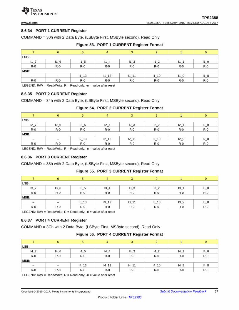
57
TPS2388www.ti.com SLUSC25A –FEBRUARY 2015–REVISED AUGUST 2017
Product Folder Links: TPS2388
Submit Documentation FeedbackCopyright © 2015–2017, Texas Instruments Incorporated
8.6.34 PORT 1 CURRENT RegisterCOMMAND = 30h with 2 Data Byte, (LSByte First, MSByte second), Read Only
Figure 53. PORT 1 CURRENT Register Format
7 6 5 4 3 2 1 0LSB:
I1_7 I1_6 I1_5 I1_4 I1_3 I1_2 I1_1 I1_0R-0 R-0 R-0 R-0 R-0 R-0 R-0 R-0
MSB:– – I1_13 I1_12 I1_11 I1_10 I1_9 I1_8
R-0 R-0 R-0 R-0 R-0 R-0 R-0 R-0LEGEND: R/W = Read/Write; R = Read only; -n = value after reset
8.6.35 PORT 2 CURRENT RegisterCOMMAND = 34h with 2 Data Byte, (LSByte First, MSByte second), Read Only
Figure 54. PORT 2 CURRENT Register Format
7 6 5 4 3 2 1 0LSB:
I2_7 I2_6 I2_5 I2_4 I2_3 I2_2 I2_1 I2_0R-0 R-0 R-0 R-0 R-0 R-0 R-0 R-0
MSB:– – I2_13 I2_12 I2_11 I2_10 I2_9 I2_8
R-0 R-0 R-0 R-0 R-0 R-0 R-0 R-0LEGEND: R/W = Read/Write; R = Read only; -n = value after reset
8.6.36 PORT 3 CURRENT RegisterCOMMAND = 38h with 2 Data Byte, (LSByte First, MSByte second), Read Only
Figure 55. PORT 3 CURRENT Register Format
7 6 5 4 3 2 1 0LSB:
I3_7 I3_6 I3_5 I3_4 I3_3 I3_2 I3_1 I3_0R-0 R-0 R-0 R-0 R-0 R-0 R-0 R-0
MSB:– – I3_13 I3_12 I3_11 I3_10 I3_9 I3_8
R-0 R-0 R-0 R-0 R-0 R-0 R-0 R-0LEGEND: R/W = Read/Write; R = Read only; -n = value after reset
8.6.37 PORT 4 CURRENT RegisterCOMMAND = 3Ch with 2 Data Byte, (LSByte First, MSByte second), Read Only
Figure 56. PORT 4 CURRENT Register Format
7 6 5 4 3 2 1 0LSB:
I4_7 I4_6 I4_5 I4_4 I4_3 I4_2 I4_1 I4_0R-0 R-0 R-0 R-0 R-0 R-0 R-0 R-0
MSB:– – I4_13 I4_12 I4_11 I4_10 I4_9 I4_8
R-0 R-0 R-0 R-0 R-0 R-0 R-0 R-0LEGEND: R/W = Read/Write; R = Read only; -n = value after reset
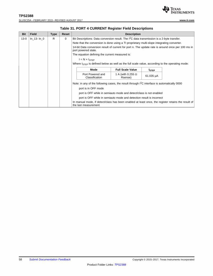
58
TPS2388SLUSC25A –FEBRUARY 2015–REVISED AUGUST 2017 www.ti.com
Product Folder Links: TPS2388
Submit Documentation Feedback Copyright © 2015–2017, Texas Instruments Incorporated
Table 31. PORT 4 CURRENT Register Field DescriptionsBit Field Type Reset Description
13-0 In_13- In_0 R 0 Bit Descriptions: Data conversion result. The I2C data transmission is a 2-byte transfer.Note that the conversion is done using a TI proprietary multi-slope integrating converter.14-bit Data conversion result of current for port n. The update rate is around once per 100 ms inport powered state.The equation defining the current measured is:
I = N × ISTEP
Where ISTEP is defined below as well as the full scale value, according to the operating mode:
Mode Full Scale Value ISTEP
Port Powered andClassification
1 A (with 0.255 ΩRsense) 61.035 µA
Note: in any of the following cases, the result through I2C interface is automatically 0000
port is in OFF mode
port is OFF while in semiauto mode and detect/class is not enabled
port is OFF while in semiauto mode and detection result is incorrectIn manual mode, if detect/class has been enabled at least once, the register retains the result ofthe last measurement

59
TPS2388www.ti.com SLUSC25A –FEBRUARY 2015–REVISED AUGUST 2017
Product Folder Links: TPS2388
Submit Documentation FeedbackCopyright © 2015–2017, Texas Instruments Incorporated
8.6.38 PORT 1 VOLTAGE RegisterCOMMAND = 32h with 2 Data Byte, (LSByte First, MSByte second), Read Only
Figure 57. PORT 1 VOLTAGE Register Format
7 6 5 4 3 2 1 0LSB:
V1_7 V1_6 V1_5 V1_4 V1_3 V1_2 V1_1 V1_0R-0 R-0 R-0 R-0 R-0 R-0 R-0 R-0
MSB:– – V1_13 V1_12 V1_11 V1_10 V1_9 V1_8
R-0 R-0 R-0 R-0 R-0 R-0 R-0 R-0LEGEND: R/W = Read/Write; R = Read only; -n = value after reset
8.6.39 PORT 2 VOLTAGE RegisterCOMMAND = 36h with 2 Data Byte, (LSByte First, MSByte second), Read Only
Figure 58. PORT 2 VOLTAGE Register Format
7 6 5 4 3 2 1 0LSB:
V2_7 V2_6 V2_5 V2_4 V2_3 V2_2 V2_1 V2_0R-0 R-0 R-0 R-0 R-0 R-0 R-0 R-0
MSB:– – V2_13 V2_12 V2_11 V2_10 V2_9 V2_8
R-0 R-0 R-0 R-0 R-0 R-0 R-0 R-0LEGEND: R/W = Read/Write; R = Read only; -n = value after reset
8.6.40 PORT 3 VOLTAGE RegisterCOMMAND = 3Ah with 2 Data Byte, (LSByte First, MSByte second), Read Only
Figure 59. PORT 3 VOLTAGE Register Format
7 6 5 4 3 2 1 0LSB:
V3_7 V3_6 V3_5 V3_4 V3_3 V3_2 V3_1 V3_0R-0 R-0 R-0 R-0 R-0 R-0 R-0 R-0
MSB:– – V3_13 V3_12 V3_11 V3_10 V3_9 V3_8
R-0 R-0 R-0 R-0 R-0 R-0 R-0 R-0LEGEND: R/W = Read/Write; R = Read only; -n = value after reset
8.6.41 PORT 4 VOLTAGE RegisterCOMMAND = 3Eh with 2 Data Byte, (LSByte First, MSByte second), Read Only
Figure 60. PORT 4 VOLTAGE Register Format
7 6 5 4 3 2 1 0LSB:
V4_7 V4_6 V4_5 V4_4 V4_3 V4_2 V4_1 V4_0R-0 R-0 R-0 R-0 R-0 R-0 R-0 R-0
MSB:– – V4_13 V4_12 V4_11 V4_10 V4_9 V4_8
R-0 R-0 R-0 R-0 R-0 R-0 R-0 R-0LEGEND: R/W = Read/Write; R = Read only; -n = value after reset

60
TPS2388SLUSC25A –FEBRUARY 2015–REVISED AUGUST 2017 www.ti.com
Product Folder Links: TPS2388
Submit Documentation Feedback Copyright © 2015–2017, Texas Instruments Incorporated
Table 32. PORT 4 VOLTAGE Register Field DescriptionsBit Field Type Reset Description
13-0 Vn_13- Vn_0 R 0 Bit Descriptions: Data conversion result. The I2C data transmission is a 2-byte transfer.The equation defining the voltage measured is:
V = N × VSTEP
Where VSTEP is defined below as well as the full scale value:
Mode Full Scale Value VSTEP
Port Powered 60 V 3.662 mV
Note that a powered port voltage measurement is made between VPWR and DRAINn.Note: if a port is OFF, the result through I2C interface is automatically 0000.
8.6.42 PoE Plus RegisterCOMMAND = 40h with1 Data Byte Read/Write
Figure 61. PoE Plus Register Format
7 6 5 4 3 2 1 0PoEP4 PoEP3 PoEP2 PoEP1 – – – TPONR/W-0 R/W-0 R/W-0 R/W-0 – – – R/W-0
LEGEND: R/W = Read/Write; R = Read only; -n = value after reset
Table 33. PoE Plus Register Field DescriptionsBit Field Type Reset Description7–4 PoEP4- PoEP1 R/W 0 When set, this activates the PoE Plus mode for a port which increases its ILIM and ISHORT
levels to around 2 ½ times their normal settings, as shown in Figure 18. Also the PoE Plus bitis used with the Police Configuration register to define ICUT threshold. See PoliceConfiguration register for more details on the subject. Note that the fault timer starts when theILIM or ICUT (if ICUT is enabled) threshold is exceeded. Also see the Port Power Priority/ICUTDisable register.Notes:1) At port turn on, the inrush current profile remains the same, whatever the state of the
PoEPn bit, as shown in Figure 17.2) When a PoEPn bit is set, the corresponding POLn bits in Police Configuration register are
initially changed to 0x0. When a PoEPn bit is reset, the corresponding POLn bits in PoliceConfiguration register are initially changed to 0xF. In both cases, the port police currentthreshold is the same value.
3) When a PoEPn bit is deasserted, the tLIM used for the associated port is always thenominal value (~60 ms). If PoEPn bit is asserted, then tLIM for associated port isprogrammable as defined in the Timing Configuration register.
4) If a port is turned on by use of the Type 2 IEEE Power Enable Pushbutton, the PSE doesthe following. When power-on is complete and if class 4 has been detected, thecorresponding PoEPn bit is set and the value of the corresponding Police Configurationregister is set to 640 mA (08h code). This is done within 5 ms of completion of inrush.
0 TPON R/W 0 When set, if DETn bit (DETECT/CLASS ENABLE register) is set and while in semiauto mode,writing a 1 at a PWONn bit in the Power Enable register will turn on a port after the currentdetection (and class is valid if enabled) cycle is completed but only if the IEEE802.3 TPONtiming specification can be met. TPON specification is the time from the completion of a validdetection cycle to port turn ON.If TPON specification cannot be met, a new detection cycle is restarted, followed by aclassification cycle, at the end of which the port is turned on, but only if a valid detection isreturned. For this case, there is no additional attempt to turn on the port until this push buttonis reasserted.If TPON bit is low, writing a 1 at a PWONn bit in the Power Enable register will turn on theassociated port immediately, regardless of IEEE802.3 TPON timing specification andregardless of the detection result.

61
TPS2388www.ti.com SLUSC25A –FEBRUARY 2015–REVISED AUGUST 2017
Product Folder Links: TPS2388
Submit Documentation FeedbackCopyright © 2015–2017, Texas Instruments Incorporated
8.6.43 FIRMWARE REVISIONCOMMAND = 41h with 1 Data Byte, Read Only
Figure 62. FIRMWARE REVISION Register Format
7 6 5 4 3 2 1 0FRV
LEGEND: R/W = Read/Write; R = Read only; -n = value after reset
Table 34. FIRMWARE REVISION Register Field DescriptionsBit Field Type Reset Description7–0 FRV R Firmware Revision number
8.6.44 I2C WATCHDOG RegisterCOMMAND = 42h with 1 Data Byte, Read/Write
The I2C watchdog timer monitors the I2C clock line in order to prevent hung software situations that could leaveports in a hazardous state. The timer can be reset by either edge on SCL input. If the watchdog timer expires, allports will be turned off and WDS bit will be set. The nominal watchdog time-out period is 2 seconds.
Figure 63. I2C WATCHDOG Register Format
7 6 5 4 3 2 1 0– – – IWDD3 IWDD2 IWDD1 IWDD0 WDS– – – R/W-1 R/W-0 R/W-1 R/W-1 R/W-0
LEGEND: R/W = Read/Write; R = Read only; -n = value after reset
Table 35. I2C WATCHDOG Register Field DescriptionsBit Field Type Reset Description4–1 IWDD3–IWDD0 R/W 1011b I2C Watchdog disable. When equal to 1011b, the watchdog is masked. Otherwise, it is
umasked and the watchdog is operational.0 WDS R/W 0 I2C Watchdog timer status, valid even if the watchdog is masked. When set, it means that
the watchdog timer has expired without any activity on I2C clock line. Writing 0 at WDSlocation clears it. Note that when the watchdog timer expires and if the watchdog isunmasked, all ports are also turned off.
When the ports are turned OFF due to I2C watchdog, the corresponding bits in Detection Event register (CLSCn,DETCn), Fault Event register (DISFn, ICUTn), Start Event register (STRTn, ILIMn), Port n Status register(CLASS Pn, DETECT Pn), DETECT/CLASS ENABLE register (CLEn, DETEn) and Power-on Fault register (PFn)are also cleared.
The corresponding PGCn and PECn bits of Power Event register will also be set if there is a change. Thecorresponding PEn and PGn bits of Power Status Register are also updated accordingly.
NOTEIf the I2C watchdog timer has expired, the Temperature and Input voltage registers willstop being updated until the WDS bit is cleared. The WDS bit must then be cleared toallow these registers to work normally.

62
TPS2388SLUSC25A –FEBRUARY 2015–REVISED AUGUST 2017 www.ti.com
Product Folder Links: TPS2388
Submit Documentation Feedback Copyright © 2015–2017, Texas Instruments Incorporated
8.6.45 DEVICE ID RegisterCOMMAND = 43h with 1 Data Byte, Read Only
Figure 64. DEVICE ID Register Format
7 6 5 4 3 2 1 0DID SR
LEGEND: R/W = Read/Write; R = Read only; -n = value after reset
Table 36. DEVICE ID Register Field DescriptionsBit Field Type Reset Description7–5 DID R 110b Device ID number (110)4–0 SR R Silicon Revision number
8.6.46 PORT 1 DETECT RESISTANCE RegisterCOMMAND = 44h with 1 Data Byte, Read Only
Figure 65. PORT 1 DETECT RESISTANCE Register Format
7 6 5 4 3 2 1 0R1_7 R1_6 R1_5 R1_4 R1_3 R1_2 R1_1 R1_0R-0 R-0 R-0 R-0 R-0 R-0 R-0 R-0
LEGEND: R/W = Read/Write; R = Read only; -n = value after reset
8.6.47 PORT 2 DETECT RESISTANCE RegisterCOMMAND = 45h with 1 Data Byte, Read Only
Figure 66. PORT 2 DETECT RESISTANCE Register Format
7 6 5 4 3 2 1 0R2_7 R2_6 R2_5 R2_4 R2_3 R2_2 R2_1 R2_0R-0 R-0 R-0 R-0 R-0 R-0 R-0 R-0
LEGEND: R/W = Read/Write; R = Read only; -n = value after reset
8.6.48 PORT 3 DETECT RESISTANCE RegisterCOMMAND = 46h with 1 Data Byte, Read Only
Figure 67. PORT 3 DETECT RESISTANCE Register Format
7 6 5 4 3 2 1 0R3_7 R3_6 R3_5 R3_4 R3_3 R3_2 R3_1 R3_0R-0 R-0 R-0 R-0 R-0 R-0 R-0 R-0
LEGEND: R/W = Read/Write; R = Read only; -n = value after reset
8.6.49 PORT 4 DETECT RESISTANCE RegisterCOMMAND = 47h with 1 Data Byte, Read Only
Figure 68. PORT 4 DETECT RESISTANCE Register Format
7 6 5 4 3 2 1 0R4_7 R4_6 R4_5 R4_4 R4_3 R4_2 R4_1 R4_0R-0 R-0 R-0 R-0 R-0 R-0 R-0 R-0
LEGEND: R/W = Read/Write; R = Read only; -n = value after reset

63
TPS2388www.ti.com SLUSC25A –FEBRUARY 2015–REVISED AUGUST 2017
Product Folder Links: TPS2388
Submit Documentation FeedbackCopyright © 2015–2017, Texas Instruments Incorporated
Table 37. PORT 4 DETECT RESISTANCE Register Field DescriptionsBit Field Type Reset Description7-0 Rn_7- Rn_0 R 0 8-bit data conversion result of detection resistance for port n.
Most recent 2-point Detection Resistance measurement result. The I2C data transmission is a1-byte transfer.Note that the register content is not cleared at port turn off.The equation defining the resistance measured is:
R = N × RSTEP
Where RSTEP is defined below as well as the full scale value:
Useable Resistance Range RSTEP
2 kΩ to 50 kΩ 195.3125 Ω

64
TPS2388SLUSC25A –FEBRUARY 2015–REVISED AUGUST 2017 www.ti.com
Product Folder Links: TPS2388
Submit Documentation Feedback Copyright © 2015–2017, Texas Instruments Incorporated
9 Application and Implementation
NOTEInformation in the following applications sections is not part of the TI componentspecification, and TI does not warrant its accuracy or completeness. TI’s customers areresponsible for determining suitability of components for their purposes. Customers shouldvalidate and test their design implementation to confirm system functionality.
9.1 Application Information
9.1.1 Introduction to PoEPower-over-Ethernet (PoE) is a means of distributing power to Ethernet devices over the Ethernet cable usingeither data or spare pairs. PoE eliminates the need for power supplies at the Ethernet device. Commonapplications of PoE are security cameras, IP Phones and PDA chargers. The host or mid-span equipment thatsupplies power is the power source equipment (PSE). The load at the Ethernet connector is the powered device(PD). PoE protocol between PSE and PD controlling power to the load is specified by IEEE Std 802.3at-2009.Transformers are used at Ethernet host ports, mid-spans and hubs, to interface data to the cable. A DC voltagecan be applied to the center tap of the transformer with no effect on the data signals. As in any powertransmission line, a relatively high 48 V is used to keep current low, minimize the effect of IR drops in the lineand preserve power to the load. Standard POE delivers approximately 13 W to a type 1 PD, and 25.5 W to atype 2 PD.
9.1.2 TPS2388 ApplicationThe TPS2388 is an 8-port, IEEE 802.3at PoE PSE controller and can be used in high port count semiauto or fullymicro-controller managed applications (The MSP430G2553 micro-controller is recommended for mostapplications). Subsequent sections describe detailed design procedures for applications with differentrequirements including host control.
The schematic of Figure 71 depicts semiauto mode operation of the TPS2388, providing functionality to powerPoE loads. In Figure 71 the TPS2388 can do the following:1. Performs load detection.2. Performs classification including type-2 (two-finger) of up to Class 4 loads.3. Enables power with protective foldback current limiting, and POLICE (ICUT) value.4. Shuts down in the event of fault loads and shorts.5. Performs Maintain Power Signature function to insure removal of power if load is disconnected.6. Undervoltage lock out occurs if VPWR falls below VPUV_F (typical 26.5 V).
Following a power-off command, disconnect or shutdown due to a start, ICUT or ILIM fault, the port powersdown. Following port power off due to a power off command or disconnect, the TPS2388 will restart a detectioncycle if commanded to do so through I2C bus. If the shutdown is due to a start, ICUT or ILIM fault, the TPS2388enters into a cool-down period during which any Detect/Class Enable Command for that port will be delayed. Atthe end of cool down cycle, one or more detection/class cycles are automatically restarted if the class and/ordetect enable bits are set.
9.1.3 Kelvin Current Sensing ResistorLoad current in each PSE port is sensed as the voltage across a low-end current-sense resistor with a value of255 mΩ. For more accurate current sensing, kelvin sensing of the low end of the current-sense resistor isprovided through pins KSENSA for ports 1 and 2, KSENSB for ports 3 and 4, KSENSC for ports 5 and 6 andKSENSD for ports 7 and 8.

14
12
13
11 KSENSB
SEN4
DRAIN4
GAT4 2
3
1
4KSENSA
GAT1
DRAIN1
SEN1
QP1
255m:
Port 4 not used
SCL
VPWR
SENn
GATn
DRAINn
DGND
INT
TPS2388SDAO
SDAI
AGND
KSENSx
VDD
+48V+3.3V
PORT100 nF100V
Note: only port n shown
255 mO
65
TPS2388www.ti.com SLUSC25A –FEBRUARY 2015–REVISED AUGUST 2017
Product Folder Links: TPS2388
Submit Documentation FeedbackCopyright © 2015–2017, Texas Instruments Incorporated
Application Information (continued)
Figure 69. Kelvin Current-Sense Connection
9.1.4 Connections on Unused PortsOn unused ports, it is recommended to ground the SENx pin and leave the GATx pin open. DRAINx pins can begrounded or left open (leaving open may slightly reduce power consumption). Figure 70 shows an example of anunused PORT4.
Figure 70. Unused PORT4 Connections

14
12
13
11
8
10
9
46
45
55
54
53
44
43 VDD
SCL
SDAI
SDAO
DGND
SEN3
DRAIN3
GAT3
KSENSB
SEN4
DRAIN4
GAT4 2
3
1
4
6
5
7
21
51
50
49
48
56
17VPWR
OSS
A1
A2
A3
A4
AGND
GAT2
DRAIN2
SEN2
KSENSA
GAT1
DRAIN1
SEN1
RESET
INT
CVDD CVPWR
DP2A CP2
QP2
RS2A RS2B
FP2
VPWRP2
+
-
RJ45
&
XFMR
DP1A CP1
QP1
RS1A RS1B
FP1
VPWR
P1
+
-RJ45
&
XFMR
TPS2388RTQ
DP3ACP3
QP3
RS3ARS3B
FP3
VPWRP3
+
-
RJ45
&
XFMR
DP4ACP4
QP4
RS4ARS4B
FP4
VPWR
P4
+
-RJ45
&
XFMR
VPWRVDD
42
40
41
39
36
38
37 SEN7
DRAIN7
GAT7
KSENSD
SEN8
DRAIN8
GAT8 30
31
29
32
34
33
35GAT6
DRAIN6
SEN6
KSENSC
GAT5
DRAIN5
SEN5
DP6A CP6
QP6
RS6A RS6B
FP6
VPWRP6
+
-
RJ45
&
XFMR
DP5A CP5
QP5
RS5A RS5B
FP5
VPWR
P5
+
-RJ45
&
XFMR
DP7ACP7
QP7
RS7ARS7B
FP7
VPWRP7
+
-
RJ45
&
XFMR
DP8ACP8
QP8
RS8ARS8B
FP8
VPWR
P8
+
-RJ45
&
XFMR
I2C Host
Device
RSCL RSDA
VDD
RRST RINT
66
TPS2388SLUSC25A –FEBRUARY 2015–REVISED AUGUST 2017 www.ti.com
Product Folder Links: TPS2388
Submit Documentation Feedback Copyright © 2015–2017, Texas Instruments Incorporated
9.2 Typical ApplicationThis typical application shows an eight port, semiauto mode application using MSP430 microcontroller. Operationin any mode requires I2C host support. The TPS2388 provides useful telemetry in multi-port applications to aid inimplementing port power management.
Figure 71. Eight Port Semiauto Mode Application

67
TPS2388www.ti.com SLUSC25A –FEBRUARY 2015–REVISED AUGUST 2017
Product Folder Links: TPS2388
Submit Documentation FeedbackCopyright © 2015–2017, Texas Instruments Incorporated
Typical Application (continued)9.2.1 Design RequirementsThe RESET pin may be connected to the micro-controller if an external RESET is required or connected directlyto VDD. TPS2388 devices are used in the eight port configuration and are managed by the I2C host device. TheI2C address for TPS2388 is programmed using the A4..A1 pins.
9.2.2 Detailed Design Procedure
9.2.2.1 Power Pin Bypass Capacitors• CVPWR: 0.1 μF, 100 V, X7R ceramic at pin 17 (VPWR)• CVDD: 0.1 μF, 50 V, X7R ceramic at pin 43 (VDD)
9.2.2.2 Per Port Components• CPn: 0.1-μF, 100-V, X7R ceramic between VPWR and Pn-• RSnA / RSnB: The port current sense resistors are a combination of two 0.51-Ω, 1% resistors in parallel (0.255
Ω). Dual 0.51-Ω, 1%, 0.25-W resistors in an 0805 SMT package are recommended. If a nominal 640 mAPolicing (ICUT) threshold is selected, the maximum power dissipation for the resistor pair becomesapproximately 115 mW (~57 mW each).
• QPn: The port MOSFET can be a small, inexpensive device with average performance characteristics. BVDSSshould be 100 V minimum. Target a MOSFET RDS(on) at VGS = 10 V of between 50 mΩ and 150 mΩ. TheMOSFET GATE charge (QG) and input capacitance (CISS) should be less than 50 nC and 2000 pFrespectively. The maximum power dissipation for QPn with RDS(on) = 100 mΩ at 640 mA nominal policing(ICUT) threshold is approximately 45 mW.
• FPn: The port fuse should be a slow blow type rated for at least 60 VDC and above ~2 x ICUT(max). The coldresistance should be below 200 mΩ to reduce the DC losses. The power dissipation for FPn with a coldresistance of 180 mΩ at maximum ICUT is approximately 81 mW.
• DPnA: The port TVS should be rated for the expected port surge environment. DPnA should have a minimumreverse standoff voltage of 58 V, peak pulse power rating of 600 W, and a maximum clamping voltage of lessthan 95 V at the expected peak surge current
9.2.2.3 System Level Components (not shown in the schematic diagrams)The system TVS and bulk VPWR capacitance work together to protect the PSE system from surge events whichcould cause VPWR to surge above 70 V. The TVS and bulk capacitors should be placed on the PCB such thatall TPS2388 ports are adequately protected.• TVS: The system TVS should have a minimum reverse standoff voltage of 58 V and a peak pulse power
rating of 600 W or 1500 W depending on the total number of system ports and amount of bulk VPWRcapacitance used. Together with the VPWR bulk capacitance, the TVS must prevent the VPWR rail fromexceeding 70 V.
• Bulk Capacitor: The system bulk capacitor(s) should be rated for 100 V and can be of aluminum electrolytictype. Two 47-μF capacitors can be used for each TPS2388 on board.
• Distributed Capacitance:In higher port count systems, it may be necessary to distribute 1-uF, 100-V, X7Rceramic capacitors across the 48-V power bus. One capacitor per each TPS2388 pair is recommended.
• Digital I/O Pullup Resistors: RESET and A1-A4 are internally pulled up to VDD, while OSS is internallypulled down, each with a 50-kΩ (typical) resistor. A stronger pull-up/down resistor can be added externallysuch as a 10 kΩ, 1%, 0.063 W type in a SMT package. SCL, SDAI, SDAO, and INT require external pull-upresistors within a range of 1 kΩ to 10 kΩ depending on the total number of devices on the bus .
• Ethernet Data Transformer (per port): The Ethernet data transformer must be rated to operate within theIEEE802.3at standard in the presence of the DC port current conditions. The transformer is also chosen to becompatible with the Ethernet PHY. The transformer may also be integrated into the RJ45 connector and cableterminations.
• RJ45 Connector (per port): The majority of the RJ45 connector requirements are mechanical in nature andinclude tab orientation, housing type (shielded or unshielded), or highly integrated. An integrated RJ45consists of the Ethernet data transformer and cable terminations at a minimum. The integrated type may alsocontain the port TVS and common mode EMI filtering.
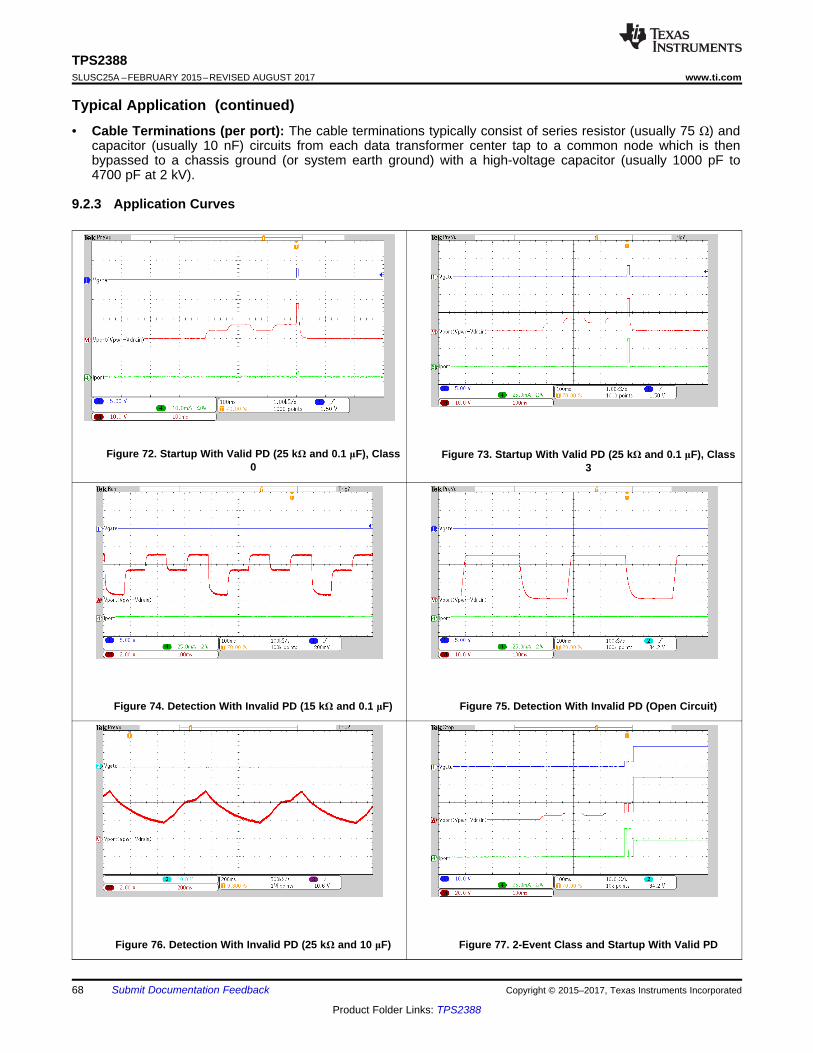
68
TPS2388SLUSC25A –FEBRUARY 2015–REVISED AUGUST 2017 www.ti.com
Product Folder Links: TPS2388
Submit Documentation Feedback Copyright © 2015–2017, Texas Instruments Incorporated
Typical Application (continued)• Cable Terminations (per port): The cable terminations typically consist of series resistor (usually 75 Ω) and
capacitor (usually 10 nF) circuits from each data transformer center tap to a common node which is thenbypassed to a chassis ground (or system earth ground) with a high-voltage capacitor (usually 1000 pF to4700 pF at 2 kV).
9.2.3 Application Curves
Figure 72. Startup With Valid PD (25 kΩ and 0.1 μF), Class0
Figure 73. Startup With Valid PD (25 kΩ and 0.1 μF), Class3
Figure 74. Detection With Invalid PD (15 kΩ and 0.1 μF) Figure 75. Detection With Invalid PD (Open Circuit)
Figure 76. Detection With Invalid PD (25 kΩ and 10 μF) Figure 77. 2-Event Class and Startup With Valid PD
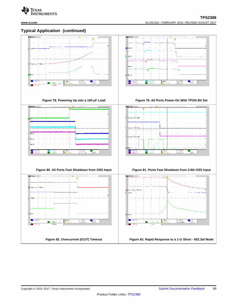
69
TPS2388www.ti.com SLUSC25A –FEBRUARY 2015–REVISED AUGUST 2017
Product Folder Links: TPS2388
Submit Documentation FeedbackCopyright © 2015–2017, Texas Instruments Incorporated
Typical Application (continued)
Figure 78. Powering Up into a 100-μF Load Figure 79. All Ports Power-On With TPON Bit Set
Figure 80. All Ports Fast Shutdown from OSS Input Figure 81. Ports Fast Shutdown from 3-Bit OSS Input
Figure 82. Overcurrent (ICUT) Timeout Figure 83. Rapid Response to a 1-Ω Short - 802.3af Mode

70
TPS2388SLUSC25A –FEBRUARY 2015–REVISED AUGUST 2017 www.ti.com
Product Folder Links: TPS2388
Submit Documentation Feedback Copyright © 2015–2017, Texas Instruments Incorporated
Typical Application (continued)
Figure 84. Rapid Response to a 1-Ω Short - PoE+ Mode Figure 85. Response to a 50-Ω Load - 802.3af Mode
Figure 86. Response to a 25-Ω Load - PoE+ Mode Figure 87. Current Limit Timeout - 802.3af Mode, 85-ΩLoad
Figure 88. Current Limit 15-ms Timeout - PoE+ Mode, 45-ΩLoad
Figure 89. Inrush Fault Timeout - 100-Ω Load
CLS1 MRK1 CLS2 MRK2
Two-event class (class 4 current)
DRAIN
GATE
SENSE
I-PORT
Inrush current
Load current
DRAIN
GATE
SENSE
I-PORT
Searching for PD
DRAIN
GATE
PD detected
PD classified
DRAIN
GATE
71
TPS2388www.ti.com SLUSC25A –FEBRUARY 2015–REVISED AUGUST 2017
Product Folder Links: TPS2388
Submit Documentation FeedbackCopyright © 2015–2017, Texas Instruments Incorporated
Typical Application (continued)
Figure 90. Current Limit Timeout Restart Delay Figure 91. Response to 8-mA to 6-mA Load, DCDisconnect Enabled
Figure 92. Detection With Open Circuit Figure 93. Detection, 2-Event Class and Port Turn On
Figure 94. 2-Event Class and Port Turn On Figure 95. 2-Event Class and Port Turn On

72
TPS2388SLUSC25A –FEBRUARY 2015–REVISED AUGUST 2017 www.ti.com
Product Folder Links: TPS2388
Submit Documentation Feedback Copyright © 2015–2017, Texas Instruments Incorporated
10 Power Supply Recommendations
10.1 VDDThe recommended VDD supply voltage requirement is 3.3 V, ±0.3 V. TPS2388 requires approximately 6 mAtypical and 12 mA maximum from the VDD supply. The VDD supply can be generated from VPWR with a buck-type regulator (LM5007 or LM5019 based) for a higher port count PSE using multiple TPS2388 devices operatingin semiauto mode. The power supply design must ensure the VDD rail rises monotonically through the VDDUVLO thresholds without any droop under the UVLO_fall threshold as the loads are turned on. This isaccomplished with proper bulk capacitance across the VDD rail for the expected load current steps over worstcase design corners. Furthermore, the combination of decoupling capacitance and bulk storage capacitancemust hold the VDD rail above the UVLO_fall threshold during any expected transient outages once power isapplied.
10.2 VPWRThe recommended VPWR supply voltage requirement is 44 V to 57 V. A power supply with a nominal 48-V or54-V output can support both type 1 and type 2 PD requirements. The output current required from the VPWRsupply depends on the number and type of ports required in the system. The TPS2388 can be configured fortype 1 and type 2 ports and the current limit is set proportionally. ICUT is programmable, for example for a type 1port it can be 380 mA , ±5%, while for a type 2 port it can be 640 mA, ±5%. Size the VPWR supply accordinglyfor the number and type of ports to be supported. As an example, the VPWR power supply rating should begreater than 3.2 A for eight type 1 ports or greater than 5.5 A for eight type 2 ports, assuming maximum port andstandby currents.
11 Layout
11.1 Layout Guidelines
11.1.1 Port Current Kelvin SensingKSENSA is shared between SEN1 and SEN2, KSENSB is shared between SEN3 and SEN4, KSENSC is sharedbetween SEN5 and SEN6, and KSENSD is shared between SEN7 and SEN8. To optimize the accuracy of themeasurement, the PCB layout must be done carefully to minimize impact of PCB trace resistance. Refer to as anexample.
Figure 96. Kelvin Sense Layout Example

RD
RN
4
FP3
CP3 CP2
DP3A
DP
3B
DP
2B
GNDP3 P2
RS1A
QP1
QP2
QP4
QP3
TPS2388RTQ
KSENSB
KSENSA
VP
WR
RS1B
RS4A
RS4B
QP8
QP7
QP5
QP6
RS8A
RS8B
RS5A
RS5B
KSENSC
KSENSD
73
TPS2388www.ti.com SLUSC25A –FEBRUARY 2015–REVISED AUGUST 2017
Product Folder Links: TPS2388
Submit Documentation FeedbackCopyright © 2015–2017, Texas Instruments Incorporated
11.2 Layout Example
Figure 97. Eight Port Layout Example (Top Side)
11.2.1 Component Placement and Routing Guidelines
11.2.1.1 Power Pin Bypass Capacitors• CVPWR: Place close to pin 17 (VPWR) and connect with low inductance traces and vias according to
Figure 97.• CVDD: Place close to pin 43 (VDD) and connect with low inductance traces and vias according to Figure 97
11.2.1.2 Per-Port Components• RSnA / RSnB: Place according to in a manner that facilitates a clean Kelvin connection with KSENSEA/B/C/D.• QPn: Place QPn around the TPS2388 as illustrated in Figure 97. Provide sufficient copper from QPn drain to
FPn.• FPn, CPn, DPnA, DPnB: Place this circuit group near the RJ45 port connector (or port power interface if a
daughter board type of interface is used as illustrated in Figure 97). Connect this circuit group to QPn drain orGND (TPS2388- AGND) using low inductance traces.

74
TPS2388SLUSC25A –FEBRUARY 2015–REVISED AUGUST 2017 www.ti.com
Product Folder Links: TPS2388
Submit Documentation Feedback Copyright © 2015–2017, Texas Instruments Incorporated
12 Device and Documentation Support
12.1 Receiving Notification of Documentation UpdatesTo receive notification of documentation updates, navigate to the device product folder on ti.com. In the upperright corner, click on Alert me to register and receive a weekly digest of any product information that haschanged. For change details, review the revision history included in any revised document.
12.2 Community ResourcesThe following links connect to TI community resources. Linked contents are provided "AS IS" by the respectivecontributors. They do not constitute TI specifications and do not necessarily reflect TI's views; see TI's Terms ofUse.
TI E2E™ Online Community TI's Engineer-to-Engineer (E2E) Community. Created to foster collaborationamong engineers. At e2e.ti.com, you can ask questions, share knowledge, explore ideas and helpsolve problems with fellow engineers.
Design Support TI's Design Support Quickly find helpful E2E forums along with design support tools andcontact information for technical support.
12.3 TrademarksE2E is a trademark of Texas Instruments.All other trademarks are the property of their respective owners.
12.4 Electrostatic Discharge CautionThis integrated circuit can be damaged by ESD. Texas Instruments recommends that all integrated circuits be handled withappropriate precautions. Failure to observe proper handling and installation procedures can cause damage.
ESD damage can range from subtle performance degradation to complete device failure. Precision integrated circuits may be moresusceptible to damage because very small parametric changes could cause the device not to meet its published specifications.
12.5 GlossarySLYZ022 — TI Glossary.
This glossary lists and explains terms, acronyms, and definitions.
13 Mechanical, Packaging, and Orderable InformationThe following pages include mechanical, packaging, and orderable information. This information is the mostcurrent data available for the designated devices. This data is subject to change without notice and revision ofthis document. For browser-based versions of this data sheet, refer to the left-hand navigation.

PACKAGE OPTION ADDENDUM
www.ti.com 13-Jan-2018
Addendum-Page 1
PACKAGING INFORMATION
Orderable Device Status(1)
Package Type PackageDrawing
Pins PackageQty
Eco Plan(2)
Lead/Ball Finish(6)
MSL Peak Temp(3)
Op Temp (°C) Device Marking(4/5)
Samples
TPS2388RTQR ACTIVE QFN RTQ 56 2000 Green (RoHS& no Sb/Br)
CU NIPDAU Level-3-260C-168 HR -40 to 125 TPS2388RTQ
TPS2388RTQT ACTIVE QFN RTQ 56 250 Green (RoHS& no Sb/Br)
CU NIPDAU Level-3-260C-168 HR -40 to 125 TPS2388RTQ
(1) The marketing status values are defined as follows:ACTIVE: Product device recommended for new designs.LIFEBUY: TI has announced that the device will be discontinued, and a lifetime-buy period is in effect.NRND: Not recommended for new designs. Device is in production to support existing customers, but TI does not recommend using this part in a new design.PREVIEW: Device has been announced but is not in production. Samples may or may not be available.OBSOLETE: TI has discontinued the production of the device.
(2) RoHS: TI defines "RoHS" to mean semiconductor products that are compliant with the current EU RoHS requirements for all 10 RoHS substances, including the requirement that RoHS substancedo not exceed 0.1% by weight in homogeneous materials. Where designed to be soldered at high temperatures, "RoHS" products are suitable for use in specified lead-free processes. TI mayreference these types of products as "Pb-Free".RoHS Exempt: TI defines "RoHS Exempt" to mean products that contain lead but are compliant with EU RoHS pursuant to a specific EU RoHS exemption.Green: TI defines "Green" to mean the content of Chlorine (Cl) and Bromine (Br) based flame retardants meet JS709B low halogen requirements of <=1000ppm threshold. Antimony trioxide basedflame retardants must also meet the <=1000ppm threshold requirement.
(3) MSL, Peak Temp. - The Moisture Sensitivity Level rating according to the JEDEC industry standard classifications, and peak solder temperature.
(4) There may be additional marking, which relates to the logo, the lot trace code information, or the environmental category on the device.
(5) Multiple Device Markings will be inside parentheses. Only one Device Marking contained in parentheses and separated by a "~" will appear on a device. If a line is indented then it is a continuationof the previous line and the two combined represent the entire Device Marking for that device.
(6) Lead/Ball Finish - Orderable Devices may have multiple material finish options. Finish options are separated by a vertical ruled line. Lead/Ball Finish values may wrap to two lines if the finishvalue exceeds the maximum column width.
Important Information and Disclaimer:The information provided on this page represents TI's knowledge and belief as of the date that it is provided. TI bases its knowledge and belief on informationprovided by third parties, and makes no representation or warranty as to the accuracy of such information. Efforts are underway to better integrate information from third parties. TI has taken andcontinues to take reasonable steps to provide representative and accurate information but may not have conducted destructive testing or chemical analysis on incoming materials and chemicals.TI and TI suppliers consider certain information to be proprietary, and thus CAS numbers and other limited information may not be available for release.
In no event shall TI's liability arising out of such information exceed the total purchase price of the TI part(s) at issue in this document sold by TI to Customer on an annual basis.

PACKAGE OPTION ADDENDUM
www.ti.com 13-Jan-2018
Addendum-Page 2

TAPE AND REEL INFORMATION
*All dimensions are nominal
Device PackageType
PackageDrawing
Pins SPQ ReelDiameter
(mm)
ReelWidth
W1 (mm)
A0(mm)
B0(mm)
K0(mm)
P1(mm)
W(mm)
Pin1Quadrant
TPS2388RTQR QFN RTQ 56 2000 330.0 16.4 8.3 8.3 1.1 12.0 16.0 Q2
TPS2388RTQT QFN RTQ 56 250 180.0 16.4 8.3 8.3 1.1 12.0 16.0 Q2
PACKAGE MATERIALS INFORMATION
www.ti.com 25-Aug-2017
Pack Materials-Page 1
*All dimensions are nominal
Device Package Type Package Drawing Pins SPQ Length (mm) Width (mm) Height (mm)
TPS2388RTQR QFN RTQ 56 2000 367.0 367.0 38.0
TPS2388RTQT QFN RTQ 56 250 210.0 185.0 35.0
PACKAGE MATERIALS INFORMATION
www.ti.com 25-Aug-2017
Pack Materials-Page 2
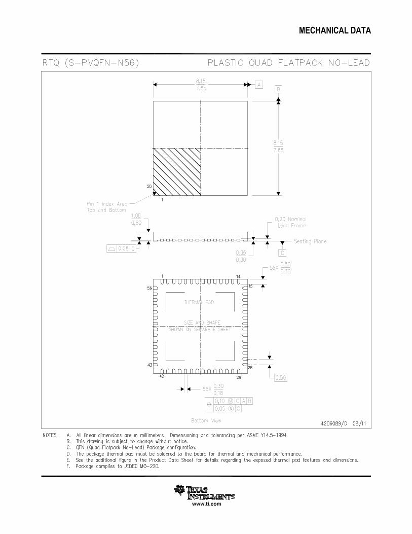

IMPORTANT NOTICE
Texas Instruments Incorporated (TI) reserves the right to make corrections, enhancements, improvements and other changes to itssemiconductor products and services per JESD46, latest issue, and to discontinue any product or service per JESD48, latest issue. Buyersshould obtain the latest relevant information before placing orders and should verify that such information is current and complete.TI’s published terms of sale for semiconductor products (http://www.ti.com/sc/docs/stdterms.htm) apply to the sale of packaged integratedcircuit products that TI has qualified and released to market. Additional terms may apply to the use or sale of other types of TI products andservices.Reproduction of significant portions of TI information in TI data sheets is permissible only if reproduction is without alteration and isaccompanied by all associated warranties, conditions, limitations, and notices. TI is not responsible or liable for such reproduceddocumentation. Information of third parties may be subject to additional restrictions. Resale of TI products or services with statementsdifferent from or beyond the parameters stated by TI for that product or service voids all express and any implied warranties for theassociated TI product or service and is an unfair and deceptive business practice. TI is not responsible or liable for any such statements.Buyers and others who are developing systems that incorporate TI products (collectively, “Designers”) understand and agree that Designersremain responsible for using their independent analysis, evaluation and judgment in designing their applications and that Designers havefull and exclusive responsibility to assure the safety of Designers' applications and compliance of their applications (and of all TI productsused in or for Designers’ applications) with all applicable regulations, laws and other applicable requirements. Designer represents that, withrespect to their applications, Designer has all the necessary expertise to create and implement safeguards that (1) anticipate dangerousconsequences of failures, (2) monitor failures and their consequences, and (3) lessen the likelihood of failures that might cause harm andtake appropriate actions. Designer agrees that prior to using or distributing any applications that include TI products, Designer willthoroughly test such applications and the functionality of such TI products as used in such applications.TI’s provision of technical, application or other design advice, quality characterization, reliability data or other services or information,including, but not limited to, reference designs and materials relating to evaluation modules, (collectively, “TI Resources”) are intended toassist designers who are developing applications that incorporate TI products; by downloading, accessing or using TI Resources in anyway, Designer (individually or, if Designer is acting on behalf of a company, Designer’s company) agrees to use any particular TI Resourcesolely for this purpose and subject to the terms of this Notice.TI’s provision of TI Resources does not expand or otherwise alter TI’s applicable published warranties or warranty disclaimers for TIproducts, and no additional obligations or liabilities arise from TI providing such TI Resources. TI reserves the right to make corrections,enhancements, improvements and other changes to its TI Resources. TI has not conducted any testing other than that specificallydescribed in the published documentation for a particular TI Resource.Designer is authorized to use, copy and modify any individual TI Resource only in connection with the development of applications thatinclude the TI product(s) identified in such TI Resource. NO OTHER LICENSE, EXPRESS OR IMPLIED, BY ESTOPPEL OR OTHERWISETO ANY OTHER TI INTELLECTUAL PROPERTY RIGHT, AND NO LICENSE TO ANY TECHNOLOGY OR INTELLECTUAL PROPERTYRIGHT OF TI OR ANY THIRD PARTY IS GRANTED HEREIN, including but not limited to any patent right, copyright, mask work right, orother intellectual property right relating to any combination, machine, or process in which TI products or services are used. Informationregarding or referencing third-party products or services does not constitute a license to use such products or services, or a warranty orendorsement thereof. Use of TI Resources may require a license from a third party under the patents or other intellectual property of thethird party, or a license from TI under the patents or other intellectual property of TI.TI RESOURCES ARE PROVIDED “AS IS” AND WITH ALL FAULTS. TI DISCLAIMS ALL OTHER WARRANTIES ORREPRESENTATIONS, EXPRESS OR IMPLIED, REGARDING RESOURCES OR USE THEREOF, INCLUDING BUT NOT LIMITED TOACCURACY OR COMPLETENESS, TITLE, ANY EPIDEMIC FAILURE WARRANTY AND ANY IMPLIED WARRANTIES OFMERCHANTABILITY, FITNESS FOR A PARTICULAR PURPOSE, AND NON-INFRINGEMENT OF ANY THIRD PARTY INTELLECTUALPROPERTY RIGHTS. TI SHALL NOT BE LIABLE FOR AND SHALL NOT DEFEND OR INDEMNIFY DESIGNER AGAINST ANY CLAIM,INCLUDING BUT NOT LIMITED TO ANY INFRINGEMENT CLAIM THAT RELATES TO OR IS BASED ON ANY COMBINATION OFPRODUCTS EVEN IF DESCRIBED IN TI RESOURCES OR OTHERWISE. IN NO EVENT SHALL TI BE LIABLE FOR ANY ACTUAL,DIRECT, SPECIAL, COLLATERAL, INDIRECT, PUNITIVE, INCIDENTAL, CONSEQUENTIAL OR EXEMPLARY DAMAGES INCONNECTION WITH OR ARISING OUT OF TI RESOURCES OR USE THEREOF, AND REGARDLESS OF WHETHER TI HAS BEENADVISED OF THE POSSIBILITY OF SUCH DAMAGES.Unless TI has explicitly designated an individual product as meeting the requirements of a particular industry standard (e.g., ISO/TS 16949and ISO 26262), TI is not responsible for any failure to meet such industry standard requirements.Where TI specifically promotes products as facilitating functional safety or as compliant with industry functional safety standards, suchproducts are intended to help enable customers to design and create their own applications that meet applicable functional safety standardsand requirements. Using products in an application does not by itself establish any safety features in the application. Designers mustensure compliance with safety-related requirements and standards applicable to their applications. Designer may not use any TI products inlife-critical medical equipment unless authorized officers of the parties have executed a special contract specifically governing such use.Life-critical medical equipment is medical equipment where failure of such equipment would cause serious bodily injury or death (e.g., lifesupport, pacemakers, defibrillators, heart pumps, neurostimulators, and implantables). Such equipment includes, without limitation, allmedical devices identified by the U.S. Food and Drug Administration as Class III devices and equivalent classifications outside the U.S.TI may expressly designate certain products as completing a particular qualification (e.g., Q100, Military Grade, or Enhanced Product).Designers agree that it has the necessary expertise to select the product with the appropriate qualification designation for their applicationsand that proper product selection is at Designers’ own risk. Designers are solely responsible for compliance with all legal and regulatoryrequirements in connection with such selection.Designer will fully indemnify TI and its representatives against any damages, costs, losses, and/or liabilities arising out of Designer’s non-compliance with the terms and provisions of this Notice.
Mailing Address: Texas Instruments, Post Office Box 655303, Dallas, Texas 75265Copyright © 2018, Texas Instruments Incorporated