Embed Size (px)
Citation preview
www.ti.com
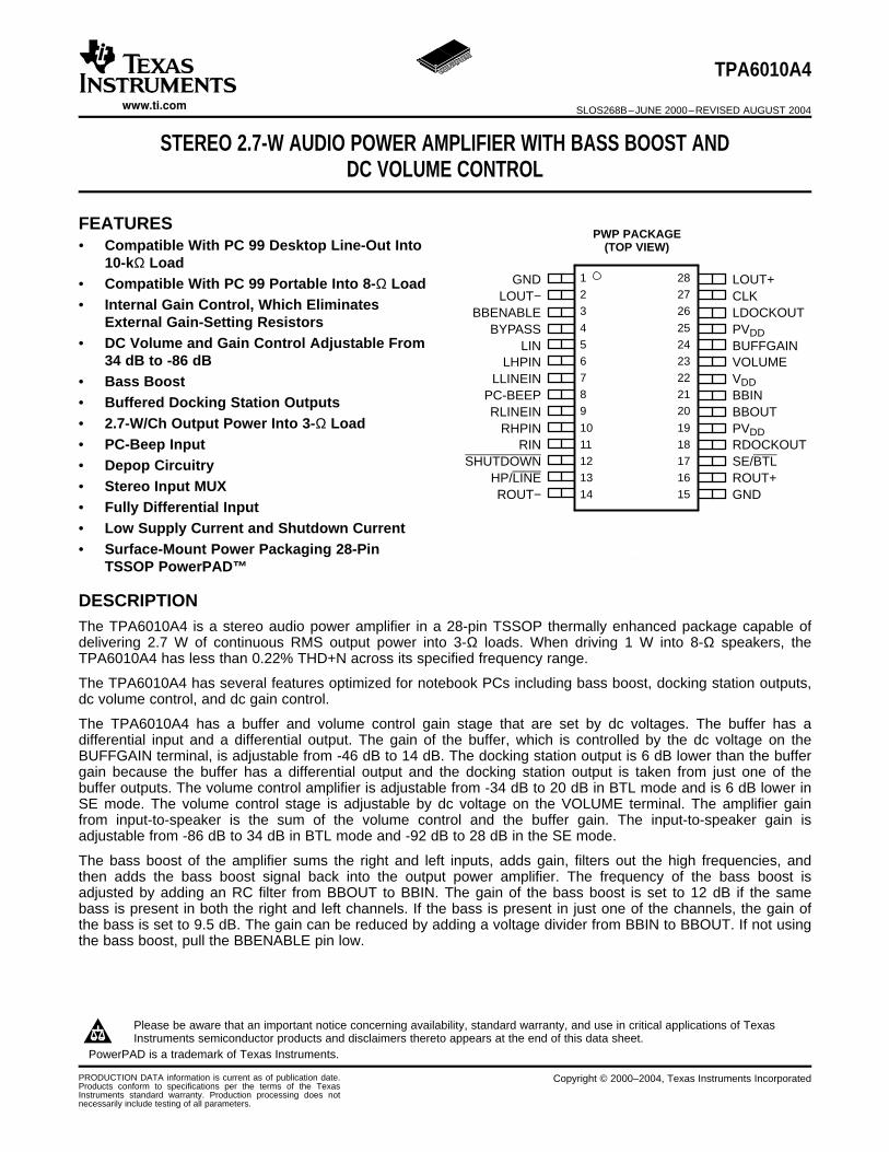
FEATURES
123
4 56789
1011121314
282726
252423222120
1918171615
GNDLOUT−
BBENABLEBYPASS
LINLHPIN
LLINEINPC-BEEPRLINEIN
RHPINRIN
SHUTDOWNHP/LINEROUT−
LOUT+CLKLDOCKOUTPVDDBUFFGAINVOLUMEVDDBBINBBOUTPVDDRDOCKOUTSE/BTLROUT+GND
DESCRIPTION
TPA6010A4
SLOS268B–JUNE 2000–REVISED AUGUST 2004
STEREO 2.7-W AUDIO POWER AMPLIFIER WITH BASS BOOST ANDDC VOLUME CONTROL
PWP PACKAGE• Compatible With PC 99 Desktop Line-Out Into (TOP VIEW)
10-kΩ Load• Compatible With PC 99 Portable Into 8-Ω Load• Internal Gain Control, Which Eliminates
External Gain-Setting Resistors• DC Volume and Gain Control Adjustable From
34 dB to -86 dB• Bass Boost• Buffered Docking Station Outputs• 2.7-W/Ch Output Power Into 3-Ω Load• PC-Beep Input• Depop Circuitry• Stereo Input MUX• Fully Differential Input• Low Supply Current and Shutdown Current• Surface-Mount Power Packaging 28-Pin
TSSOP PowerPAD™
The TPA6010A4 is a stereo audio power amplifier in a 28-pin TSSOP thermally enhanced package capable ofdelivering 2.7 W of continuous RMS output power into 3-Ω loads. When driving 1 W into 8-Ω speakers, theTPA6010A4 has less than 0.22% THD+N across its specified frequency range.
The TPA6010A4 has several features optimized for notebook PCs including bass boost, docking station outputs,dc volume control, and dc gain control.
The TPA6010A4 has a buffer and volume control gain stage that are set by dc voltages. The buffer has adifferential input and a differential output. The gain of the buffer, which is controlled by the dc voltage on theBUFFGAIN terminal, is adjustable from -46 dB to 14 dB. The docking station output is 6 dB lower than the buffergain because the buffer has a differential output and the docking station output is taken from just one of thebuffer outputs. The volume control amplifier is adjustable from -34 dB to 20 dB in BTL mode and is 6 dB lower inSE mode. The volume control stage is adjustable by dc voltage on the VOLUME terminal. The amplifier gainfrom input-to-speaker is the sum of the volume control and the buffer gain. The input-to-speaker gain isadjustable from -86 dB to 34 dB in BTL mode and -92 dB to 28 dB in the SE mode.
The bass boost of the amplifier sums the right and left inputs, adds gain, filters out the high frequencies, andthen adds the bass boost signal back into the output power amplifier. The frequency of the bass boost isadjusted by adding an RC filter from BBOUT to BBIN. The gain of the bass boost is set to 12 dB if the samebass is present in both the right and left channels. If the bass is present in just one of the channels, the gain ofthe bass is set to 9.5 dB. The gain can be reduced by adding a voltage divider from BBIN to BBOUT. If not usingthe bass boost, pull the BBENABLE pin low.
Please be aware that an important notice concerning availability, standard warranty, and use in critical applications of TexasInstruments semiconductor products and disclaimers thereto appears at the end of this data sheet.
PowerPAD is a trademark of Texas Instruments.
PRODUCTION DATA information is current as of publication date. Copyright © 2000–2004, Texas Instruments IncorporatedProducts conform to specifications per the terms of the TexasInstruments standard warranty. Production processing does notnecessarily include testing of all parameters.

www.ti.com
+
−RHPIN R
MUXRLINEINRIN
Σ
Σ
BassBoost
PVDD
PowerManagement
VDD
PC-BEEPPC
BEEP
BYPASS
SHUTDOWN
GND
SE/BTL MUXCONTROLHP/LINE
ROUT+
RDOCKOUT
ROUT−
BBOUT
BBIN
RBB
CBB
BBENABLE
LHPIN LMUXLLINEIN
LINLOUT+
LDOCKOUT
LOUT−
BUFFGAIN VOLUME
DC GAINand Volume
Control
BUFFGAIN
VOLUME
CLK
+
−
+
−
Σ
+
−
Σ
+
−
+
−
+
−
Σ
BUFFGAIN VOLUME
+
−
+
−
+
−
Σ
TPA6010A4
SLOS268B–JUNE 2000–REVISED AUGUST 2004
The PowerPAD package (PWP) delivers a level of thermal performance that was previously achievable only inTO-220-type packages. Thermal impedances of approximately 35°C/W are truly realized in multilayer PCBapplications. This allows the TPA6010A4 to operate at full power into 8-Ω loads at ambient temperatures of85°C.
FUNCTIONAL BLOCK DIAGRAM
2
www.ti.com
TPA6010A4
SLOS268B–JUNE 2000–REVISED AUGUST 2004
These devices have limited built-in ESD protection. The leads should be shorted together or the deviceplaced in conductive foam during storage or handling to prevent electrostatic damage to the MOS gates.
AVAILABLE OPTIONS
PACKAGED DEVICETA TSSOP (1) (PWP)
-40°C to 85°C TPA6010A4PWP
(1) The PWP package is available taped and reeled. To order a tapedand reeled part, add the suffix R to the part number (e.g.,TPA6010A4PWPR).
Terminal Functions
TERMINALI/O DESCRIPTION
NAME NO.
BBENABLE is the bass boost control input. When this terminal is held high, the extra bass from the bassBBENABLE 3 I boost circuitry is added to the output signal. When this terminal is held low, no extra bass is added.
BBIN 21 I BBIN is the buffered input to the power amplifier from the bass boost circuitry.
BBOUT is the bass boost output. A low pass filter must be placed from BBOUT to BBIN to select the lowBBOUT 20 O frequencies to be boosted.
BYPASS 4 Tap to voltage divider for internal midsupply bias generator
If a 47-nF capacitor is attached, the TPA6010A4 generates an internal clock. An external clock canCLK 27 I override the internal clock input to this terminal.
The gain of the dockout buffer is adjustable from -52 dB to 8 dB to LDOCKOUT and RDOCKOUT, and isBUFFGAIN 24 I set by a dc voltage from 0 V to 3.54 V. When the dc level is over 3.54 V, the device is muted.
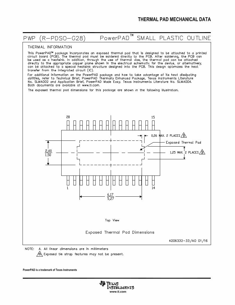
GND 1, 15 Ground connection for circuitry. Connected to thermal pad.
HP/LINE 13 I MUX control input, hold high to select LHPIN or RHPIN, hold low to select LLINEIN or RLINEIN.
LHPIN 6 I Left channel headphone input, selected when HP/LINE is held high
LIN 5 I Common left input for fully differential input. AC ground for single-ended inputs
LLINEIN 7 I Left channel line negative input, selected when HP/LINE is held low
LDOCKOUT is the buffered output of LLINEIN or LHPIN. Use BUFFGAIN for volume adjustment of thisLDOCKOUT 26 O pin.
LOUT+ 28 O Left channel positive output in BTL mode and positive output in SE mode
LOUT- 2 O Left channel negative output in BTL mode and high-impedance in SE mode
The input for PC Beep mode. PC-BEEP is enabled when a > 1.5-V (peak-to-peak) square wave is input toPC-BEEP 8 I PC-BEEP. AC ground if use is not desired.
PVDD 19, 25 I Power supply for output stage
RHPIN 10 I Right channel headphone input, selected when HP/LINE is held high
RIN 11 I Common right input for fully differential input. AC ground for single-ended inputs
RLINEIN 9 I Right channel line input, selected when HP/LINE is held low
RDOCKOUT is the buffered output of RLINEIN or RHPIN. Use BUFFGAIN for volume adjustment of thisRDOCKOUT 18 O pin.
ROUT+ 16 O Right channel positive output in BTL mode and positive output in SE mode
ROUT- 14 O Right channel negative output in BTL mode and high-impedance in SE mode
Output MUX control. When this terminal is high, SE outputs are selected. When this terminal is low, theSE/BTL 17 I BTL outputs are selected.
SHUTDOWN 12 I When held low, this terminal places the entire device, except PC-BEEP detect circuitry, in shutdown mode.
VDD 22 I Analog VDD input supply. This terminal needs to be isolated from PVDD to achieve highest performance.
VOLUME detects the dc level at the terminal and sets the gain for 31 discrete steps covering a range of 20VOLUME 23 I dB to -40 dB for dc levels of 0.15 V to 3.54. When the dc level is over 3.54 V, the device is muted.
Connect to GND. The pad must be soldered down in all applications in order to properly secure the deviceThermal Pad to the PCB.
3

www.ti.com
ABSOLUTE MAXIMUM RATINGS
DISSIPATION RATING TABLE
RECOMMENDED OPERATING CONDITIONS
ELECTRICAL CHARACTERISTICS
TPA6010A4
SLOS268B–JUNE 2000–REVISED AUGUST 2004
over operating free-air temperature range (unless otherwise noted) (1)
UNIT
VDD Supply voltage 6 V
VI Input voltage -0.3 V to VDD +0.3 V
Continuous total power dissipation Internally Limited (see Dissipation Rating Table)
TA Operating free-air temperature range -40°C to 85°C
TJ Operating junction temperature range -40°C to 150°C
Tstg Storage temperature range -65°C to 85°C
Lead temperature 1,6 mm (1/16 inch) from case for 10 seconds 260°C
(1) Stresses beyond those listed under "absolute maximum ratings" may cause permanent damage to the device. These are stress ratingsonly, and functional operation of the device at these or any other conditions beyond those indicated under "recommended operatingconditions" is not implied. Exposure to absolute-maximum-rated conditions for extended periods may affect device reliability.
PACKAGE TA ≤ 25°C DERATING FACTOR TA = 70°C TA = 85°C
PWP 2.7 W (1) 21.8 mW/°C 1.7 W 1.4 W
(1) See the Texas Instruments document, PowerPAD Thermally Enhanced Package Application Report (SLMA002), for more information onthe PowerPAD™ package. The thermal data was measured on a PCB layout based on the information in the section entitled TexasInstruments Recommended Board for PowerPAD on page 33 of the before mentioned document.
MIN MAX UNIT
VDD Supply voltage 4.5 5.5 V
SE/BTL, HP/LINE 0.8 × VDDVIH High-level input voltage VSHUTDOWN, BBENABLE 2
SE/BTL, HP/LINE 0.6 × VDDVIL Low-level input voltage VSHUTDOWN, BBENABLE 0.8
TA Operating free-air temperature -40 85 °C
at specified free-air temperature, VDD = 5 V, TA = 25°C (unless otherwise noted)
PARAMETER TEST CONDITIONS MIN TYP MAX UNIT
|VOS| Output offset voltage (measured differentially) AV = 6 dB 35 mV
PSRR Power supply rejection ratio VDD = 4.9 V to 5.1 V 67 dB
SHUTDOWN, SE/BTL, HP/LINE,|IIH| High-level input current VDD = 5.5 V, VI = VDD 1 µAVOLUME, BUFFGAIN, BBENABLE
SHUTDOWN, SE/BTL, HP/LINE,|IIL| Low-level input current VDD = 5.5 V, VI = 0 V 1 µAVOLUME, BUFFGAIN, BBENABLE
BTL mode, SHUTDOWN = 2 V, 12 18SE/BTL = 0.6 × VDDIDD Supply current mASE mode, SHUTDOWN = 2 V, 6.5 10SE/BTL = 0.8 × VDD
PC-BEEP = 2.5 V, 95 250SHUTDOWN = 0 VIDD(SD) Supply current, shutdown mode µA
PC-BEEP = 0 V, 62 200SHUTDOWN = 0 V
4
www.ti.com
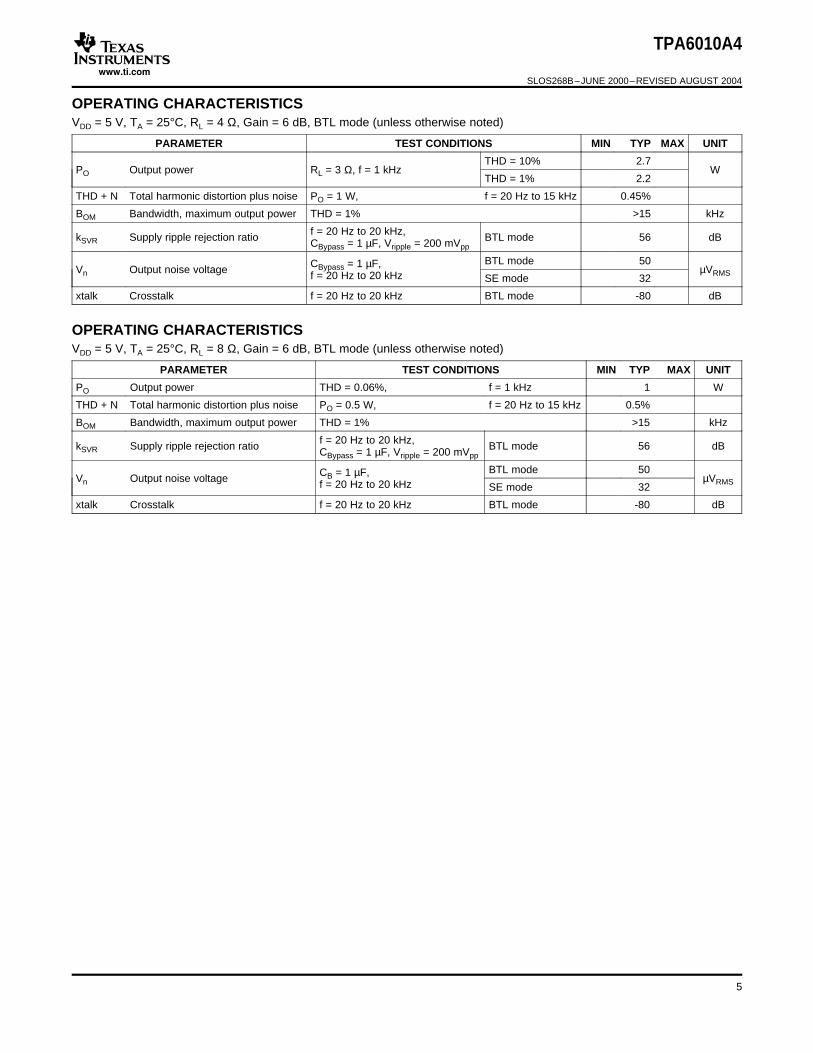
OPERATING CHARACTERISTICS
OPERATING CHARACTERISTICS
TPA6010A4
SLOS268B–JUNE 2000–REVISED AUGUST 2004
VDD = 5 V, TA = 25°C, RL = 4 Ω, Gain = 6 dB, BTL mode (unless otherwise noted)
PARAMETER TEST CONDITIONS MIN TYP MAX UNIT
THD = 10% 2.7PO Output power RL = 3 Ω, f = 1 kHz W
THD = 1% 2.2
THD + N Total harmonic distortion plus noise PO = 1 W, f = 20 Hz to 15 kHz 0.45%
BOM Bandwidth, maximum output power THD = 1% >15 kHz
f = 20 Hz to 20 kHz,kSVR Supply ripple rejection ratio BTL mode 56 dBCBypass = 1 µF, Vripple = 200 mVpp
BTL mode 50CBypass = 1 µF,Vn Output noise voltage µVRMSf = 20 Hz to 20 kHz SE mode 32
xtalk Crosstalk f = 20 Hz to 20 kHz BTL mode -80 dB
VDD = 5 V, TA = 25°C, RL = 8 Ω, Gain = 6 dB, BTL mode (unless otherwise noted)
PARAMETER TEST CONDITIONS MIN TYP MAX UNIT
PO Output power THD = 0.06%, f = 1 kHz 1 W
THD + N Total harmonic distortion plus noise PO = 0.5 W, f = 20 Hz to 15 kHz 0.5%
BOM Bandwidth, maximum output power THD = 1% >15 kHz
f = 20 Hz to 20 kHz,kSVR Supply ripple rejection ratio BTL mode 56 dBCBypass = 1 µF, Vripple = 200 mVpp
BTL mode 50CB = 1 µF,Vn Output noise voltage µVRMSf = 20 Hz to 20 kHz SE mode 32
xtalk Crosstalk f = 20 Hz to 20 kHz BTL mode -80 dB
5

www.ti.com
TYPICAL CHARACTERISTICS
Table of Graphs
0.01
0.1
1
10
10 100 200
TH
D+N
− T
ota
l Har
mo
nic
Dis
tort
ion
+ N
ois
e −
%
PO − Output Power − mW
VDD = 5 V,f = 1 kHzRL = 32 ΩSingle-EndedGain = 6 dB
500.01
0.1
1
10
0.01 0.1 1
TH
D+N
− T
ota
l Har
mo
nic
Dis
tort
ion
+ N
ois
e −
%
PO − Output Power − W
VDD = 5 V,f = 1 kHzBridge-Tied LoadGain = 6 dB
RL = 4 Ω
RL = 3 Ω
RL = 8 Ω
2 3
TPA6010A4
SLOS268B–JUNE 2000–REVISED AUGUST 2004
FIGURE
vs Output power 1,2
THD + N Total harmonic distortion + noise vs Dockout voltage 3
vs Frequency 4, 5, 6
TOTAL HARMONIC DISTORTION + NOISE TOTAL HARMONIC DISTORTION + NOISEvs vs
OUTPUT POWER OUTPUT POWER
Figure 1. Figure 2.
6

www.ti.com
0.01
0.1
1
10
0.1 1 2
TH
D+N
− T
ota
l Har
mo
nic
Dis
tort
ion
+ N
ois
e −
%
VO − Dockout Voltage − V
VDD = 5 V,RL = 10 kΩf = 1 kHzGain = 6 dB
0.5T
HD
+N −
To
tal H
arm
on
ic D
isto
rtio
n +
No
ise
− %
f − Frequency − Hz
0.01
0.1
1
10
20 100 1 k 10 k 20 k
RL = 3 Ω,PO = 2 W
RL = 4 Ω,PO = 1.5 W
RL = 8 Ω,PO = 1 W
VDD = 5 V,Bridge-Tied LoadGain = 6 dB
0.001
0.01
0.1
1
20 100 1 k 10 k 20 k
TH
D+N
− T
ota
l Har
mo
nic
Dis
tort
ion
+ N
ois
e −
%
f − Frequency − Hz
VDD = 5 V,Gain = 6 dBSingle-EndedRL = 32 ΩPO = 75 mW
TH
D+N
− T
ota
l Har
mo
nic
Dis
tort
ion
+ N
ois
e −
%
f − Frequency − Hz
VDD = 5 V,CI = 0.47 µF,RL = 10 kΩGain = 6 dB,Dockout
0.01
0.1
1
20 100 1 k 10 k 20 k
VO = 500 mVrms
VO = 1 Vrms
TPA6010A4
SLOS268B–JUNE 2000–REVISED AUGUST 2004
TOTAL HARMONIC DISTORTION + NOISE TOTAL HARMONIC DISTORTION + NOISEvs vs
DOCKOUT VOLTAGE FREQUENCY
Figure 3. Figure 4.
TOTAL HARMONIC DISTORTION + NOISE TOTAL HARMONIC DISTORTION + NOISEvs vs
FREQUENCY FREQUENCY
Figure 5. Figure 6.
7

www.ti.com
APPLICATION INFORMATION
INTERNAL BUFFER GAIN AND VOLUME GAIN
TPA6010A4
SLOS268B–JUNE 2000–REVISED AUGUST 2004
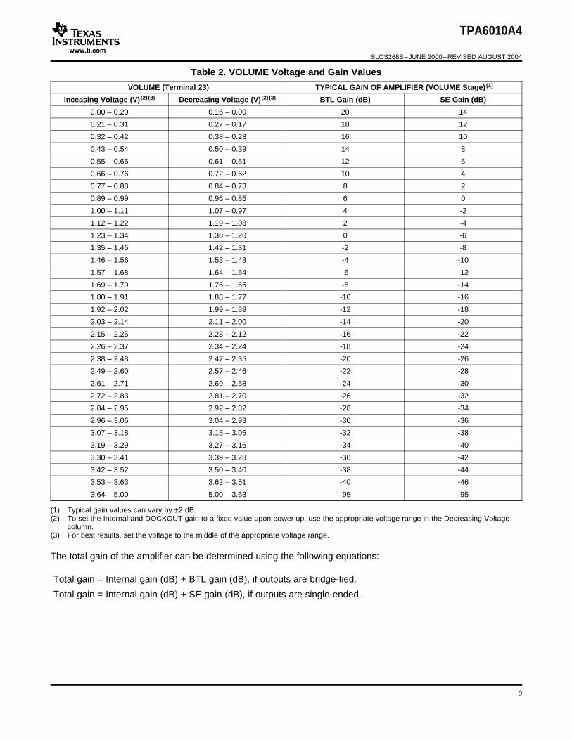
The typical voltage and gain levels are shown in Table 1 and Table 2.
Table 1. BUFFGAIN Voltage and Gain Values
BUFFGAIN (Terminal 24) TYPICAL GAIN OF AMPLIFIER (VOLUME Stage) (1)
Inceasing Voltage (V) (2) (3) Decreasing Voltage (V) (2) (3) Internal Gain (dB) DOCKOUT Gain (dB)
0.00 – 0.20 0.16 – 0.00 14 8
0.21 – 0.31 0.27 – 0.17 12 6
0.32 – 0.42 0.38 – 0.28 10 4
0.43 – 0.54 0.50 – 0.39 8 2
0.55 – 0.65 0.61 – 0.51 6 0
0.66 – 0.76 0.72 – 0.62 4 -2
0.77 – 0.88 0.84 – 0.73 2 -4
0.89 – 0.99 0.96 – 0.85 0 -6
1.00 – 1.11 1.07 – 0.97 -2 -8
1.12 – 1.22 1.19 – 1.08 -4 -10
1.23 – 1.34 1.30 – 1.20 -6 -12
1.35 – 1.45 1.42 – 1.31 -8 -14
1.46 – 1.56 1.53 – 1.43 -10 -16
1.57 – 1.68 1.64 – 1.54 -12 -18
1.69 – 1.79 1.76 – 1.65 -14 -20
1.80 – 1.91 1.88 – 1.77 -16 -22
1.92 – 2.02 1.99 – 1.89 -18 -24
2.03 – 2.14 2.11 – 2.00 -20 -26
2.15 – 2.25 2.23 – 2.12 -22 -28
2.26 – 2.37 2.34 – 2.24 -24 -30
2.38 – 2.48 2.47 – 2.35 -26 -32
2.49 – 2.60 2.57 – 2.46 -28 -34
2.61 – 2.71 2.69 – 2.58 -30 -36
2.72 – 2.83 2.81 – 2.70 -32 -38
2.84 – 2.95 2.92 – 2.82 -34 -40
2.96 – 3.06 3.04 – 2.93 -36 -42
3.07 – 3.18 3.15 – 3.05 -38 -44
3.19 – 3.29 3.27 – 3.16 -40 -46
3.30 – 3.41 3.39 – 3.28 -42 -48
3.42 – 3.52 3.50 – 3.40 -44 -50
3.53 – 3.63 3.62 – 3.51 -46 -52
3.64 – 5.00 5.00 – 3.63 -75 -81
(1) Typical gain values can vary by ±2 dB.(2) To set the Internal and DOCKOUT gain to a fixed value upon power up, use the appropriate voltage range in the Decreasing Voltage
column.(3) For best results, set the voltage to the middle of the appropriate voltage range.
8
www.ti.com
TPA6010A4
SLOS268B–JUNE 2000–REVISED AUGUST 2004
Table 2. VOLUME Voltage and Gain Values
VOLUME (Terminal 23) TYPICAL GAIN OF AMPLIFIER (VOLUME Stage) (1)
Inceasing Voltage (V) (2) (3) Decreasing Voltage (V) (2) (3) BTL Gain (dB) SE Gain (dB)
0.00 – 0.20 0.16 – 0.00 20 14
0.21 – 0.31 0.27 – 0.17 18 12
0.32 – 0.42 0.38 – 0.28 16 10
0.43 – 0.54 0.50 – 0.39 14 8
0.55 – 0.65 0.61 – 0.51 12 6
0.66 – 0.76 0.72 – 0.62 10 4
0.77 – 0.88 0.84 – 0.73 8 2
0.89 – 0.99 0.96 – 0.85 6 0
1.00 – 1.11 1.07 – 0.97 4 -2
1.12 – 1.22 1.19 – 1.08 2 -4
1.23 – 1.34 1.30 – 1.20 0 -6
1.35 – 1.45 1.42 – 1.31 -2 -8
1.46 – 1.56 1.53 – 1.43 -4 -10
1.57 – 1.68 1.64 – 1.54 -6 -12
1.69 – 1.79 1.76 – 1.65 -8 -14
1.80 – 1.91 1.88 – 1.77 -10 -16
1.92 – 2.02 1.99 – 1.89 -12 -18
2.03 – 2.14 2.11 – 2.00 -14 -20
2.15 – 2.25 2.23 – 2.12 -16 -22
2.26 – 2.37 2.34 – 2.24 -18 -24
2.38 – 2.48 2.47 – 2.35 -20 -26
2.49 – 2.60 2.57 – 2.46 -22 -28
2.61 – 2.71 2.69 – 2.58 -24 -30
2.72 – 2.83 2.81 – 2.70 -26 -32
2.84 – 2.95 2.92 – 2.82 -28 -34
2.96 – 3.06 3.04 – 2.93 -30 -36
3.07 – 3.18 3.15 – 3.05 -32 -38
3.19 – 3.29 3.27 – 3.16 -34 -40
3.30 – 3.41 3.39 – 3.28 -36 -42
3.42 – 3.52 3.50 – 3.40 -38 -44
3.53 – 3.63 3.62 – 3.51 -40 -46
3.64 – 5.00 5.00 – 3.63 -95 -95
(1) Typical gain values can vary by ±2 dB.(2) To set the Internal and DOCKOUT gain to a fixed value upon power up, use the appropriate voltage range in the Decreasing Voltage
column.(3) For best results, set the voltage to the middle of the appropriate voltage range.
The total gain of the amplifier can be determined using the following equations:
Total gain = Internal gain (dB) + BTL gain (dB), if outputs are bridge-tied.
Total gain = Internal gain (dB) + SE gain (dB), if outputs are single-ended.
9

www.ti.com
−
RHPINR
MUXRLINEINRIN
Σ
Σ
BassBoost
PVDD
PowerManagement
VDD
PC-BEEP PCBEEP
BYPASSSHUTDOWN
GND
SE/BTLMUX
CONTROLHP/LINE
ROUT+
RDOCKOUT
ROUT−
BBOUT
BBIN
RBB
CBB
BBENABLE
LHPINL
MUXLLINEINLIN
LOUT+
LDOCKOUT
LOUT−
BUFFGAIN VOLUME
DC GAINand Volume
Control
BUFFGAIN
VOLUMECLK
+
−
+
−
Σ
+
−
Σ
+
−
+
−
+−
Σ
BUFFGAIN VOLUME
+−
+
−
+
−
Σ
1 kΩ
COUTR100 µF
100 kΩ
1 kΩ
COUTL100 µF
VDD
100 kΩ
To SystemControl
18
16
14
20
21
3
28
2
26
DepopCircuitry
109
11
24
2327
19, 2522
412
1, 15
8
1713
675
CRHP0.47 µFRight
HeadphoneInput Signal CRLINE
0.47 µFCRIN
0.47 µF
Right LineInput Signal
VDD
VDD
50 kΩ
50 kΩ
CCLK47 nF
CSR0.1 µF
VDD
CSR0.1 µF
VDD CBYP0.47 µF
To SystemControl
CPCB0.47 µF
PC BeepInput Signal
CLHP0.47 µF
CLLINE0.47 µF
LeftHeadphone
Input Signal
Left LineInput Signal
CLIN0.47 µF
To Right DockingStation InputSee Note B
To Left DockingStation InputSee Note B
+
See Note A
TPA6010A4
SLOS268B–JUNE 2000–REVISED AUGUST 2004
A. A 0.1-µF ceramic capacitor should be placed as close as possible to the IC. For filtering lower-frequency noisesignals, a larger electrolytic capacitor of 10 µF or greater should be placed near the audio power amplifier.
B. A DC-blocking capacitor should be placed at each input to the amplifier in the docking station, as the RDOCKOUTand LDOCKOUT pins are biased to VDD/2.
Figure 7. Typical TPA6010A4 Application Circuit Using Single-Ended Inputs and Input MUX
10
www.ti.com
+
−
RHPINR
MUXRLINEINRIN
Σ
Σ
BassBoost
PVDD
PowerManagement
VDD
PC-BEEP PCBEEP
BYPASSSHUTDOWN
GND
SE/BTLMUX
CONTROLHP/LINE
ROUT+
RDOCKOUT
ROUT−
BBOUT
BBIN
RBB
CBB
BBENABLE
LHPINL
MUXLLINEINLIN
LOUT+
LDOCKOUT
LOUT−
BUFFGAIN VOLUME
DC GAINand Volume
Control
BUFFGAIN
VOLUMECLK
+
−
+
−
Σ
+
−
Σ
+
−
+
−
+
−
Σ
BUFFGAIN VOLUME
+
−
+
−
+
−
Σ
1 kΩ
COUTR100 µF
100 kΩ
1 kΩ
COUTL100 µF
VDD
100 kΩ
To SystemControl
18
16
14
20
21
3
28
2
26
DepopCircuitry
109
11
24
2327
19, 2522
412
1, 15
8
1713
675
CRIN+0.47 µF
Right NegativeDifferential
Input Signal
CRIN−0.47 µF
VDD
VDD
50 kΩ
50 kΩ
CCLK47 nF
CSR0.1 µF
VDD
CSR0.1 µF
VDD CBYP0.47 µF
To SystemControl
CPCB0.47 µF
PC BeepInput Signal
CLIN−0.47 µF
N/C
Right PositiveDifferential
Input Signal
N/C
CLIN+0.47 µF
Left NegativeDifferential
Input Signal
Left PositiveDifferential
Input Signal
To Right DockingStation InputSee Note B
To Left DockingStation InputSee Note B
See Note A
INPUT RESISTANCE
CIN
RI
RF
Input Signal
TPA6010A4
SLOS268B–JUNE 2000–REVISED AUGUST 2004
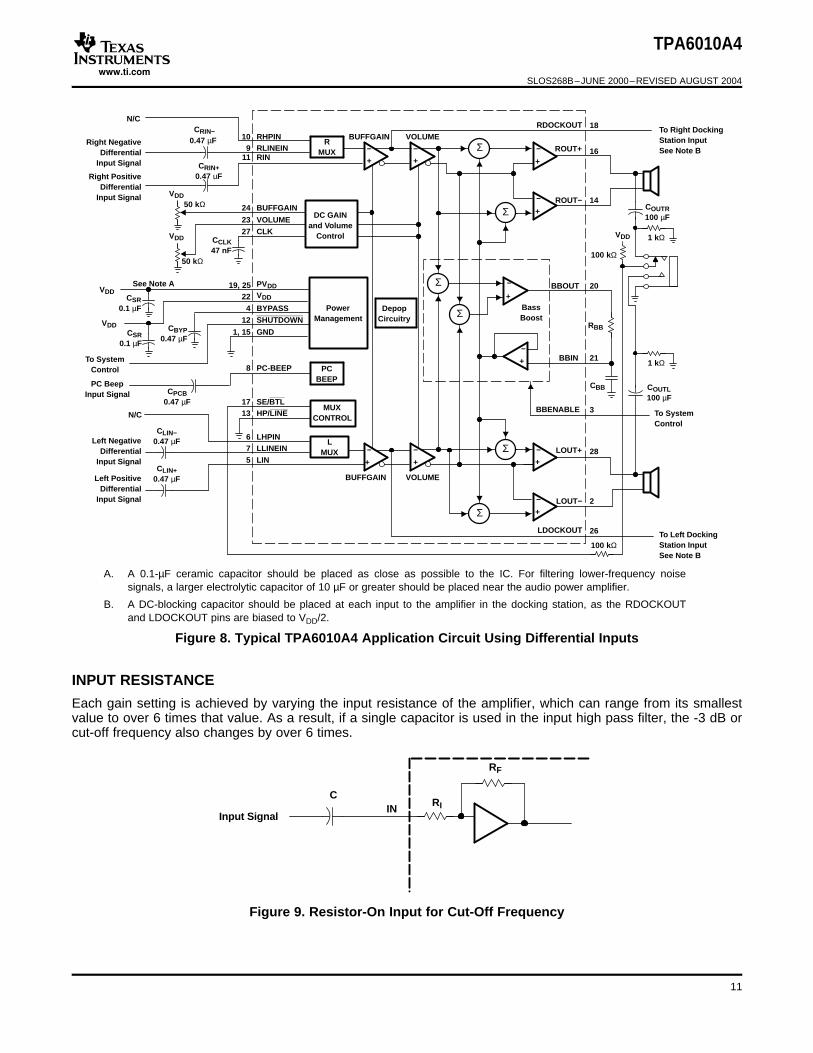
A. A 0.1-µF ceramic capacitor should be placed as close as possible to the IC. For filtering lower-frequency noisesignals, a larger electrolytic capacitor of 10 µF or greater should be placed near the audio power amplifier.
B. A DC-blocking capacitor should be placed at each input to the amplifier in the docking station, as the RDOCKOUTand LDOCKOUT pins are biased to VDD/2.
Figure 8. Typical TPA6010A4 Application Circuit Using Differential Inputs
Each gain setting is achieved by varying the input resistance of the amplifier, which can range from its smallestvalue to over 6 times that value. As a result, if a single capacitor is used in the input high pass filter, the -3 dB orcut-off frequency also changes by over 6 times.
Figure 9. Resistor-On Input for Cut-Off Frequency
11
www.ti.com
INPUT CAPACITOR, CI
fc 1
2RICI
-3 dB
fc (1)
CI 1
2RI fc (2)
POWER SUPPLY DECOUPLING, CS
MIDRAIL BYPASS CAPACITOR, CBYP
TPA6010A4
SLOS268B–JUNE 2000–REVISED AUGUST 2004
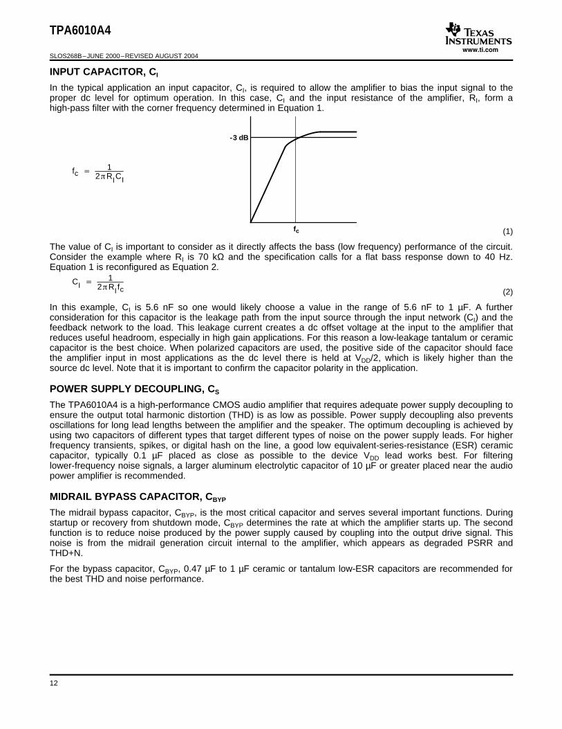
In the typical application an input capacitor, CI, is required to allow the amplifier to bias the input signal to theproper dc level for optimum operation. In this case, CI and the input resistance of the amplifier, RI, form ahigh-pass filter with the corner frequency determined in Equation 1.
The value of CI is important to consider as it directly affects the bass (low frequency) performance of the circuit.Consider the example where RI is 70 kΩ and the specification calls for a flat bass response down to 40 Hz.Equation 1 is reconfigured as Equation 2.
In this example, CI is 5.6 nF so one would likely choose a value in the range of 5.6 nF to 1 µF. A furtherconsideration for this capacitor is the leakage path from the input source through the input network (CI) and thefeedback network to the load. This leakage current creates a dc offset voltage at the input to the amplifier thatreduces useful headroom, especially in high gain applications. For this reason a low-leakage tantalum or ceramiccapacitor is the best choice. When polarized capacitors are used, the positive side of the capacitor should facethe amplifier input in most applications as the dc level there is held at VDD/2, which is likely higher than thesource dc level. Note that it is important to confirm the capacitor polarity in the application.
The TPA6010A4 is a high-performance CMOS audio amplifier that requires adequate power supply decoupling toensure the output total harmonic distortion (THD) is as low as possible. Power supply decoupling also preventsoscillations for long lead lengths between the amplifier and the speaker. The optimum decoupling is achieved byusing two capacitors of different types that target different types of noise on the power supply leads. For higherfrequency transients, spikes, or digital hash on the line, a good low equivalent-series-resistance (ESR) ceramiccapacitor, typically 0.1 µF placed as close as possible to the device VDD lead works best. For filteringlower-frequency noise signals, a larger aluminum electrolytic capacitor of 10 µF or greater placed near the audiopower amplifier is recommended.
The midrail bypass capacitor, CBYP, is the most critical capacitor and serves several important functions. Duringstartup or recovery from shutdown mode, CBYP determines the rate at which the amplifier starts up. The secondfunction is to reduce noise produced by the power supply caused by coupling into the output drive signal. Thisnoise is from the midrail generation circuit internal to the amplifier, which appears as degraded PSRR andTHD+N.
For the bypass capacitor, CBYP, 0.47 µF to 1 µF ceramic or tantalum low-ESR capacitors are recommended forthe best THD and noise performance.
12

www.ti.com
BASS BOOST OPERATION
-3 dB
fc
fc 1
2RBBCBB
(3)
Bass Boost Gain 9.5 dB 20Log R2R1 R2
Bass Boost Gain 12 dB 20Log R2R1 R2
(bass present on both channels)
(bass present on only one channel)(4)
OUTPUT COUPLING CAPACITOR, CC
fc 1
2RLCC
-3 dB
fc (5)
TPA6010A4
SLOS268B–JUNE 2000–REVISED AUGUST 2004
The bass boost feature of the TPA6010A4 sums the left and right inputs, adds gain, filters out the highfrequencies, and adds the bass-boosted signal back into the current-gain stage of the amplifier. The cutofffrequency is set by RBB and CBB as shown in Equation 3.
The gain of the bass boost is set internally at 12 dB if bass is present in both the right and left channels. If bassis only present in one of the channels, the boost is reduced to 9.5 dB.
The total bass boost gain may be determined by using Equation 4.
Consider the following example application. The desired cutoff frequency for the bass boost is 300 Hz and thedesired bass boost gain is 6 dB. The filter components could be RBB = 1.1 kΩ and CBB = 0.47 µF.
If the bass boost feature is not to be used or if the user wishes to disable the boost, the BBENABLE pin shouldbe pulled low.
Finally, as illustrated in the functional block diagram, the bass boost is only applied to the speaker outputs, not tothe docking station outputs.
In the typical single-supply SE configuration, an output coupling capacitor (CC) is required to block the dc bias atthe output of the amplifier thus preventing dc currents in the load. As with the input coupling capacitor, the outputcoupling capacitor and impedance of the load form a high-pass filter governed by Equation 5.
The main disadvantage, from a performance standpoint, is the load impedances are typically small, which drivesthe low-frequency corner higher degrading the bass response. Large values of CC are required to pass lowfrequencies into the load. Consider the example where a CC of 330 µF is chosen and loads vary from 3 Ω, 4 Ω, 8Ω, 32Ω , 10 kΩ, and 47 kΩ. Table 3 summarizes the frequency response characteristics of each configuration.
13

www.ti.com
USING LOW-ESR CAPACITORS
BRIDGED-TIED LOAD VERSUS SINGLE-ENDED MODE
Power V(rms)
2
RL
V(rms) VO(PP)
2 2
(6)
RL 2x VO(PP)
VO(PP)
-VO(PP)
VDD
VDD
TPA6010A4
SLOS268B–JUNE 2000–REVISED AUGUST 2004
Table 3. Common Load Impedances vs Low Frequency Output Characteristicsin SE Mode
RL CC LOWEST FREQUENCY
3 Ω 330 µF 161 Hz
4 Ω 330 µF 120 Hz
8 Ω 330 µF 60 Hz
32 Ω 330 µF 15 Hz
10,000 Ω 330 µF 0.05 Hz
47,000 Ω 330 µF 0.01 Hz
As Table 3 indicates, most of the bass response is attenuated into a 4-Ω load, an 8-Ω load is adequate,headphone response is good, and drive into line level inputs (a home stereo for example) is exceptional.
Low-ESR capacitors are recommended throughout this applications section. A real (as opposed to ideal)capacitor can be modeled simply as a resistor in series with an ideal capacitor. The voltage drop across thisresistor minimizes the beneficial effects of the capacitor in the circuit. The lower the equivalent value of thisresistance the more the real capacitor behaves like an ideal capacitor.
Figure 10 shows a Class-AB audio power amplifier (APA) in a BTL configuration. The TPA6010A4 BTL amplifierconsists of two Class-AB amplifiers driving both ends of the load. There are several potential benefits to thisdifferential drive configuration but initially consider power to the load. The differential drive to the speaker meansthat as one side is slewing up, the other side is slewing down, and vice versa. This in effect doubles the voltageswing on the load as compared to a ground referenced load. Plugging 2 × VO(PP) into the power equation, wherevoltage is squared, yields 4× the output power from the same supply rail and load impedance as in Equation 6.
Figure 10. Bridge-Tied Load Configuration
14

www.ti.com
fc 1
2RLCC (7)
RL
CCVO(PP)
VO(PP)
VDD
-3 dB
fc
SINGLE-ENDED OPERATION
BTL AMPLIFIER EFFICIENCY
TPA6010A4
SLOS268B–JUNE 2000–REVISED AUGUST 2004
In a typical computer sound channel operating at 5 V, bridging raises the power into an 8-Ω speaker from asingled-ended (SE, ground reference) limit of 250 mW to 1 W. In sound power that is a 6-dB improvement —which is loudness that can be heard. In addition to increased power there are frequency response concerns.Consider the single-supply SE configuration shown in Figure 11. A coupling capacitor is required to block the dcoffset voltage from reaching the load. These capacitors can be quite large (approximately 33 µF to 1000 µF) sothey tend to be expensive, heavy, occupy valuable PCB area, and have the additional drawback of limitinglow-frequency performance of the system. This frequency limiting effect is due to the high-pass filter networkcreated with the speaker impedance and the coupling capacitance and is calculated with Equation 7.
For example, a 68-µF capacitor with an 8-Ω speaker would attenuate low frequencies below 293 Hz. The BTLconfiguration cancels the dc offsets, which eliminates the need for the blocking capacitors. Low-frequencyperformance is then limited only by the input network and speaker response. Cost and PCB space are alsominimized by eliminating the bulky coupling capacitor.
Figure 11. Single-Ended Configuration and Frequency Response
Increasing power to the load does carry a penalty of increased internal power dissipation. The increaseddissipation is understandable considering that the BTL configuration produces 4× the output power of the SEconfiguration. Internal dissipation versus output power is discussed further in the CREST FACTOR andTHERMAL CONSIDERATIONS section.
In SE mode (see Figure 10 and Figure 11), the load is driven from the primary amplifier output for each channel(OUT+, terminals 28 and 16).
The amplifier switches single-ended operation when the SE/BTL terminal is held high. This puts the negativeoutputs in a high-impedance state, and reduces the amplifier's gain to 1 V/V.
Class-AB amplifiers are notoriously inefficient. The primary cause of these inefficiencies is voltage drop acrossthe output stage transistors. There are two components of the internal voltage drop. One is the headroom or dcvoltage drop that varies inversely to output power. The second component is due to the sinewave nature of theoutput. The total voltage drop can be calculated by subtracting the RMS value of the output voltage from VDD.The internal voltage drop multiplied by the RMS value of the supply current, IDDrms, determines the internalpower dissipation of the amplifier.
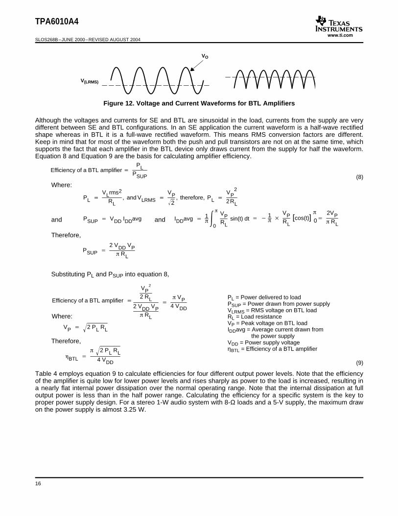
An easy-to-use equation to calculate efficiency starts out being equal to the ratio of power from the power supplyto the power delivered to the load. To accurately calculate the RMS and average values of power in the load andin the amplifier, the current and voltage waveform shapes must first be understood (see Figure 12).
15
www.ti.com
V(LRMS)
VO IDD
IDD(avg)
Efficiency of a BTL amplifier PL
PSUP (8)
PL = Power delivered to loadPSUP = Power drawn from power supplyVLRMS = RMS voltage on BTL loadRL = Load resistanceVP = Peak voltage on BTL loadIDDavg = Average current drawn from the power supplyVDD = Power supply voltageηBTL = Efficiency of a BTL amplifier
Efficiency of a BTL amplifier
VP2
2 RL2 VDD VP
RL
VP
4 VDD
VP 2 PL RL
BTL 2 PL RL
4 VDD
Where:
Therefore,
Substituting PL and PSUP into equation 8,
Where:
PL VLrms2
RL, and VLRMS
VP
2, therefore, PL
VP2
2RL
and PSUP VDD IDDavg and IDDavg 1
0
VPRL
sin(t) dt 1
VPRL
[cos(t)]
02VP RL
Therefore,
PSUP 2 VDD VP
RL
(9)
TPA6010A4
SLOS268B–JUNE 2000–REVISED AUGUST 2004
Figure 12. Voltage and Current Waveforms for BTL Amplifiers
Although the voltages and currents for SE and BTL are sinusoidal in the load, currents from the supply are verydifferent between SE and BTL configurations. In an SE application the current waveform is a half-wave rectifiedshape whereas in BTL it is a full-wave rectified waveform. This means RMS conversion factors are different.Keep in mind that for most of the waveform both the push and pull transistors are not on at the same time, whichsupports the fact that each amplifier in the BTL device only draws current from the supply for half the waveform.Equation 8 and Equation 9 are the basis for calculating amplifier efficiency.
Table 4 employs equation 9 to calculate efficiencies for four different output power levels. Note that the efficiencyof the amplifier is quite low for lower power levels and rises sharply as power to the load is increased, resulting ina nearly flat internal power dissipation over the normal operating range. Note that the internal dissipation at fulloutput power is less than in the half power range. Calculating the efficiency for a specific system is the key toproper power supply design. For a stereo 1-W audio system with 8-Ω loads and a 5-V supply, the maximum drawon the power supply is almost 3.25 W.
16
www.ti.com
CREST FACTOR AND THERMAL CONSIDERATIONS
PdB 10LogPWPref 10Log 4 W
1 W 6 dB
(10)
6 dB 15 dB 9 dB (15 dB crest factor)
6 dB 12 dB 6 dB (12 dB crest factor)
6 dB 9 dB 3 dB (9 dB crest factor)
6 dB 6 dB 0 dB (6 dB crest factor)
6 dB 3 dB 3 dB (3 dB crest factor)
PW 10PdB10 Pref
63 mW (18 dB crest factor)
125 mW (15 dB crest factor)
250 mW (9 dB crest factor)
500 mW (6 dB crest factor)
1000 mW (3 dB crest factor)
2000 mW (15 dB crest factor) (11)
TPA6010A4
SLOS268B–JUNE 2000–REVISED AUGUST 2004
Table 4. Efficiency vs Output Power in 5-V 8-Ω BTL Systems
OUTPUT PEAK INTERNALEFFICIENCYPOWER VOLTAGE DISSIPATION(%)(W) (V) (W)
0.25 31.4 2.00 0.55
0.50 44.4 2.83 0.62
1.00 62.8 4.00 0.59
1.25 70.2 4.47 (1) 0.53
(1) High peak voltages cause the THD to increase.
A final point to remember about Class-AB amplifiers (either SE or BTL) is how to manipulate the terms in theefficiency equation to the utmost advantage when possible. Note that in Equation 9, VDD is in the denominator.This indicates that as VDD goes down, efficiency goes up.
Class-AB power amplifiers dissipate a significant amount of heat in the package under normal operatingconditions. A typical music CD requires 12 dB to 15 dB of dynamic range, or headroom above the average poweroutput, to pass the loudest portions of the signal without distortion. In other words, music typically has a crestfactor between 12 dB and 15 dB. When determining the optimal ambient operating temperature, the internaldissipated power at the average output power level must be used. From the TPA6010A4 data sheet, one cansee that when the TPA6010A4 is operating from a 5-V supply into a 3-Ω speaker that 4-W peaks are available.Converting watts to dB as in Equation 10:
Subtracting the headroom restriction to obtain the average listening level without distortion yields:
Converting dB back into watts as in Equation 11:
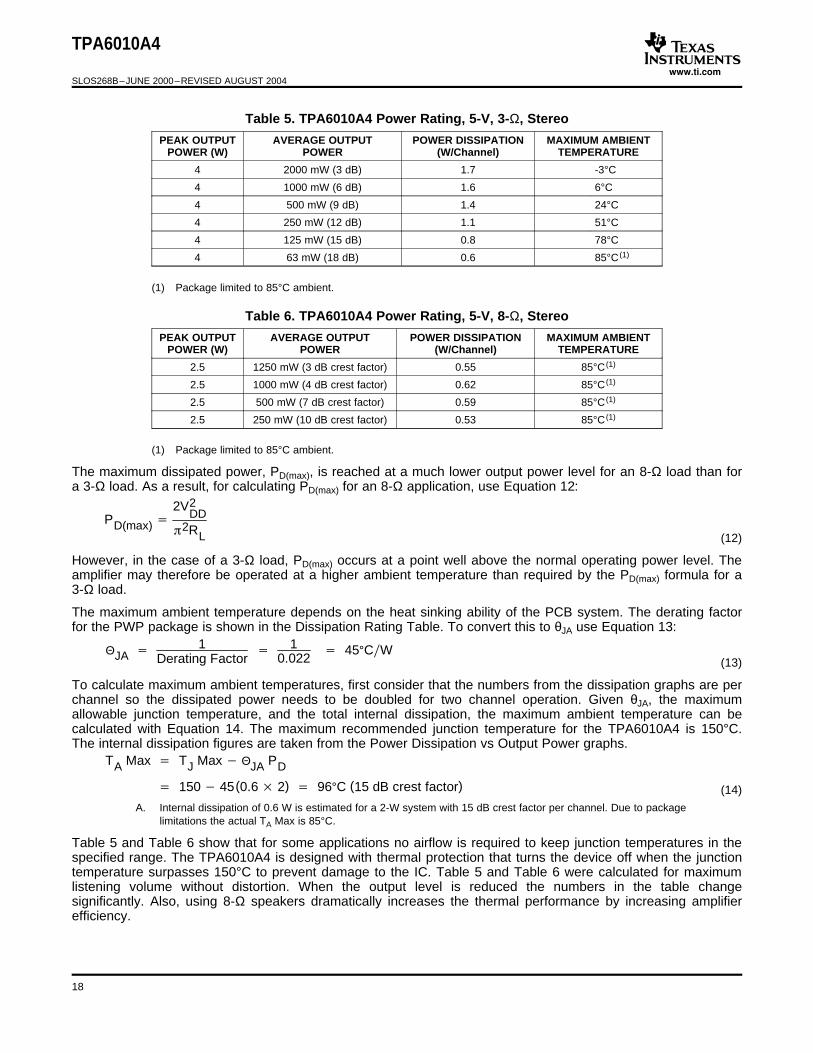
This is valuable information to consider when attempting to estimate the heat dissipation requirements for theamplifier system. Comparing the absolute worst case, which is 2 W of continuous power output with a 3 dB crestfactor, against 12 dB and 15 dB applications drastically affects maximum ambient temperature ratings for thesystem. Using the power dissipation curves for a 5-V, 3-Ω system, the internal dissipation in the TPA6010A4 andmaximum ambient temperatures are shown in Table 5.
17
www.ti.com
PD(max) 2V2
DD
2RL (12)
ΘJA 1Derating Factor
10.022
45°CW(13)
TA Max TJ Max ΘJA PD
150 45(0.6 2) 96°C (15 dB crest factor) (14)
TPA6010A4
SLOS268B–JUNE 2000–REVISED AUGUST 2004
Table 5. TPA6010A4 Power Rating, 5-V, 3-Ω, Stereo
PEAK OUTPUT AVERAGE OUTPUT POWER DISSIPATION MAXIMUM AMBIENTPOWER (W) POWER (W/Channel) TEMPERATURE
4 2000 mW (3 dB) 1.7 -3°C
4 1000 mW (6 dB) 1.6 6°C
4 500 mW (9 dB) 1.4 24°C
4 250 mW (12 dB) 1.1 51°C
4 125 mW (15 dB) 0.8 78°C
4 63 mW (18 dB) 0.6 85°C (1)
(1) Package limited to 85°C ambient.
Table 6. TPA6010A4 Power Rating, 5-V, 8-Ω, Stereo
PEAK OUTPUT AVERAGE OUTPUT POWER DISSIPATION MAXIMUM AMBIENTPOWER (W) POWER (W/Channel) TEMPERATURE
2.5 1250 mW (3 dB crest factor) 0.55 85°C (1)
2.5 1000 mW (4 dB crest factor) 0.62 85°C (1)
2.5 500 mW (7 dB crest factor) 0.59 85°C (1)
2.5 250 mW (10 dB crest factor) 0.53 85°C (1)
(1) Package limited to 85°C ambient.
The maximum dissipated power, PD(max), is reached at a much lower output power level for an 8-Ω load than fora 3-Ω load. As a result, for calculating PD(max) for an 8-Ω application, use Equation 12:
However, in the case of a 3-Ω load, PD(max) occurs at a point well above the normal operating power level. Theamplifier may therefore be operated at a higher ambient temperature than required by the PD(max) formula for a3-Ω load.
The maximum ambient temperature depends on the heat sinking ability of the PCB system. The derating factorfor the PWP package is shown in the Dissipation Rating Table. To convert this to θJA use Equation 13:
To calculate maximum ambient temperatures, first consider that the numbers from the dissipation graphs are perchannel so the dissipated power needs to be doubled for two channel operation. Given θJA, the maximumallowable junction temperature, and the total internal dissipation, the maximum ambient temperature can becalculated with Equation 14. The maximum recommended junction temperature for the TPA6010A4 is 150°C.The internal dissipation figures are taken from the Power Dissipation vs Output Power graphs.
A. Internal dissipation of 0.6 W is estimated for a 2-W system with 15 dB crest factor per channel. Due to packagelimitations the actual TA Max is 85°C.
Table 5 and Table 6 show that for some applications no airflow is required to keep junction temperatures in thespecified range. The TPA6010A4 is designed with thermal protection that turns the device off when the junctiontemperature surpasses 150°C to prevent damage to the IC. Table 5 and Table 6 were calculated for maximumlistening volume without distortion. When the output level is reduced the numbers in the table changesignificantly. Also, using 8-Ω speakers dramatically increases the thermal performance by increasing amplifierefficiency.
18

www.ti.com
SE/BTL OPERATION
+
−RHPIN
RMUXRLINEIN
RINΣ ROUT+
RDOCKOUT
ROUT−
+
−
+
−
+
−
Σ
1 kΩ
COUTR100 µF
100 kΩ
VDD
18
16
14
109
11
100 kΩ
SE/BTL 17
PC BEEP OPERATION
CPCB 1
2 fPCB (100 k)(15)
TPA6010A4
SLOS268B–JUNE 2000–REVISED AUGUST 2004
The ability of the TPA6010A4 to easily switch between BTL and SE modes is one of its most important costsaving features. This feature eliminates the requirement for an additional headphone amplifier in applicationswhere internal stereo speakers are driven in BTL mode but external headphone or speakers must beaccommodated. Internal to the TPA6010A4, two separate amplifiers drive OUT+ and OUT-. The SE/BTL input(terminal 17) controls the operation of the follower amplifier that drives LOUT- and ROUT- (terminals 2 and 14).When SE/BTL is held low, the amplifier is on and the TPA6010A4 is in the BTL mode. When SE/BTL is heldhigh, the OUT- amplifiers are in a high output impedance state, which configures the TPA6010A4 as an SEdriver from LOUT+ and ROUT+ (terminals 28 and 16). IDD is reduced by approximately one-half in SE mode.Control of the SE/BTL input can be from a logic-level CMOS source or, more typically, from a resistor dividernetwork as shown in Figure 13.
Figure 13. TPA6010A4 Resistor Divider Network Circuit
Using a readily available 1/8-in. (3.5 mm) stereo headphone jack, the control switch is closed when no plug isinserted. When closed the 100-kΩ/1-kΩ divider pulls the SE/BTL input low. When a plug is inserted, the 1-kΩresistor is disconnected and the SE/BTL input is pulled high. When the input goes high, the OUT- amplifier isshut down causing the speaker to mute (virtually open-circuits the speaker). The OUT+ amplifier then drivesthrough the output capacitor (CO) into the headphone jack.
The PC BEEP input allows a system beep to be sent directly from a computer through the amplifier to thespeakers with few external components. The input is activated automatically. When the PC BEEP input is active,both of the LINEIN and HPIN inputs are deselected and both the left and right channels are driven in BTL modewith the signal from PC BEEP. The gain from the PC BEEP input to the speakers is fixed at 0.3 V/V and isindependent of the volume setting. When the PC BEEP input is deselected, the amplifier returns to the previousoperating mode and volume setting. Furthermore, if the amplifier is in shutdown mode, activating PC BEEP takesthe device out of shutdown and outputs the PC BEEP signal, and then returns the amplifier to shutdown mode.
The amplifier automatically switches to PC BEEP mode after detecting a valid signal at the PC BEEP input. Thepreferred input signal is a square wave or pulse train with an amplitude of 1.5 Vpp or greater. To be accuratelydetected, the signal must have a minimum of 1.5-Vpp amplitude, rise and fall times of less than 0.1 µs, and aminimum of 8 rising edges. When the signal is no longer detected, the amplifier returns to its previous operatingmode and volume setting.
If it is desired to ac-couple the PC BEEP input, the value of the coupling capacitor should be chosen to satisfyEquation 15:
The PC BEEP input can also be dc-coupled to avoid using this coupling capacitor. The pin normally sits atmidrail when no signal is present.
19
www.ti.com
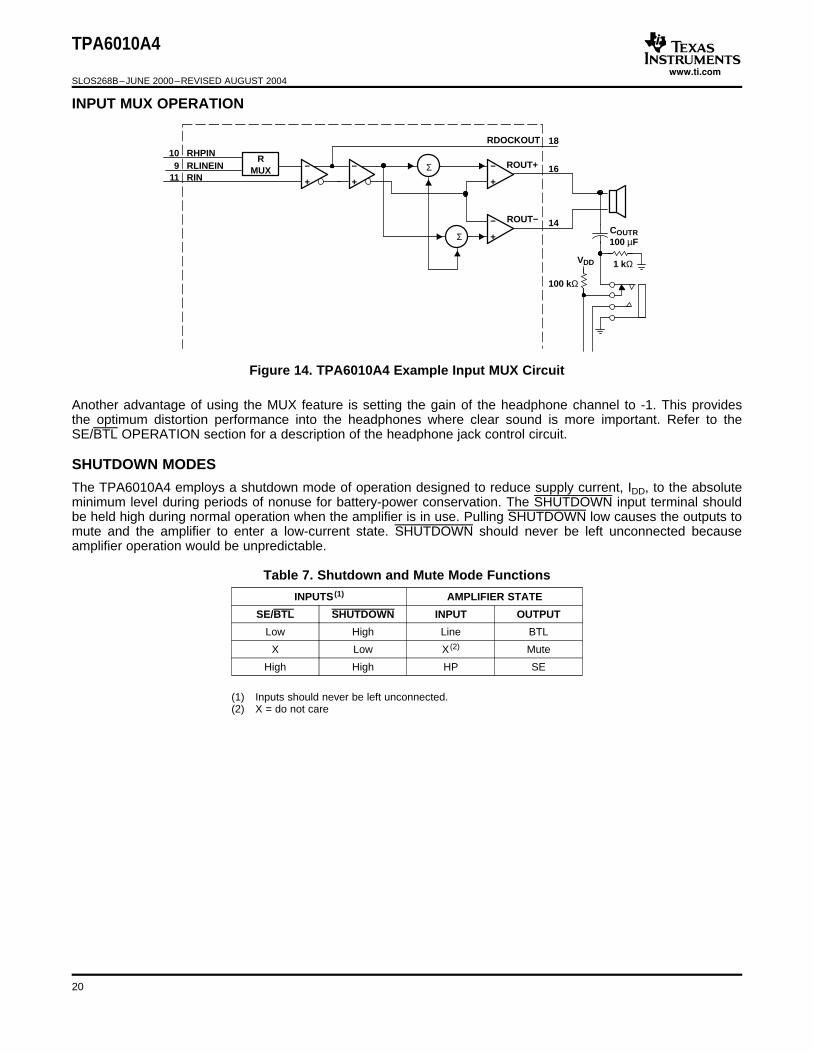
INPUT MUX OPERATION
+
−RHPIN
RMUXRLINEIN
RINΣ ROUT+
RDOCKOUT
ROUT−
+
−
+
−
+
−
Σ
1 kΩ
COUTR100 µF
100 kΩ
VDD
18
16
14
109
11
SHUTDOWN MODES
TPA6010A4
SLOS268B–JUNE 2000–REVISED AUGUST 2004
Figure 14. TPA6010A4 Example Input MUX Circuit
Another advantage of using the MUX feature is setting the gain of the headphone channel to -1. This providesthe optimum distortion performance into the headphones where clear sound is more important. Refer to theSE/BTL OPERATION section for a description of the headphone jack control circuit.
The TPA6010A4 employs a shutdown mode of operation designed to reduce supply current, IDD, to the absoluteminimum level during periods of nonuse for battery-power conservation. The SHUTDOWN input terminal shouldbe held high during normal operation when the amplifier is in use. Pulling SHUTDOWN low causes the outputs tomute and the amplifier to enter a low-current state. SHUTDOWN should never be left unconnected becauseamplifier operation would be unpredictable.
Table 7. Shutdown and Mute Mode Functions
INPUTS (1) AMPLIFIER STATE
SE/BTL SHUTDOWN INPUT OUTPUT
Low High Line BTL
X Low X (2) Mute
High High HP SE
(1) Inputs should never be left unconnected.(2) X = do not care
20

PACKAGE OPTION ADDENDUM
www.ti.com 11-Apr-2013
Addendum-Page 1
PACKAGING INFORMATION
Orderable Device Status(1)
Package Type PackageDrawing
Pins PackageQty
Eco Plan(2)
Lead/Ball Finish MSL Peak Temp(3)
Op Temp (°C) Top-Side Markings(4)
Samples
TPA6010A4PWP ACTIVE HTSSOP PWP 28 50 Green (RoHS& no Sb/Br)
CU NIPDAU Level-3-260C-168 HR -40 to 85 TPA6010
TPA6010A4PWPR ACTIVE HTSSOP PWP 28 2000 Green (RoHS& no Sb/Br)
CU NIPDAU Level-3-260C-168 HR -40 to 85 TPA6010
(1) The marketing status values are defined as follows:ACTIVE: Product device recommended for new designs.LIFEBUY: TI has announced that the device will be discontinued, and a lifetime-buy period is in effect.NRND: Not recommended for new designs. Device is in production to support existing customers, but TI does not recommend using this part in a new design.PREVIEW: Device has been announced but is not in production. Samples may or may not be available.OBSOLETE: TI has discontinued the production of the device.
(2) Eco Plan - The planned eco-friendly classification: Pb-Free (RoHS), Pb-Free (RoHS Exempt), or Green (RoHS & no Sb/Br) - please check http://www.ti.com/productcontent for the latest availabilityinformation and additional product content details.TBD: The Pb-Free/Green conversion plan has not been defined.Pb-Free (RoHS): TI's terms "Lead-Free" or "Pb-Free" mean semiconductor products that are compatible with the current RoHS requirements for all 6 substances, including the requirement thatlead not exceed 0.1% by weight in homogeneous materials. Where designed to be soldered at high temperatures, TI Pb-Free products are suitable for use in specified lead-free processes.Pb-Free (RoHS Exempt): This component has a RoHS exemption for either 1) lead-based flip-chip solder bumps used between the die and package, or 2) lead-based die adhesive used betweenthe die and leadframe. The component is otherwise considered Pb-Free (RoHS compatible) as defined above.Green (RoHS & no Sb/Br): TI defines "Green" to mean Pb-Free (RoHS compatible), and free of Bromine (Br) and Antimony (Sb) based flame retardants (Br or Sb do not exceed 0.1% by weightin homogeneous material)
(3) MSL, Peak Temp. -- The Moisture Sensitivity Level rating according to the JEDEC industry standard classifications, and peak solder temperature.
(4) Multiple Top-Side Markings will be inside parentheses. Only one Top-Side Marking contained in parentheses and separated by a "~" will appear on a device. If a line is indented then it is acontinuation of the previous line and the two combined represent the entire Top-Side Marking for that device.
Important Information and Disclaimer:The information provided on this page represents TI's knowledge and belief as of the date that it is provided. TI bases its knowledge and belief on informationprovided by third parties, and makes no representation or warranty as to the accuracy of such information. Efforts are underway to better integrate information from third parties. TI has taken andcontinues to take reasonable steps to provide representative and accurate information but may not have conducted destructive testing or chemical analysis on incoming materials and chemicals.TI and TI suppliers consider certain information to be proprietary, and thus CAS numbers and other limited information may not be available for release.
In no event shall TI's liability arising out of such information exceed the total purchase price of the TI part(s) at issue in this document sold by TI to Customer on an annual basis.

TAPE AND REEL INFORMATION
*All dimensions are nominal
Device PackageType
PackageDrawing
Pins SPQ ReelDiameter
(mm)
ReelWidth
W1 (mm)
A0(mm)
B0(mm)
K0(mm)
P1(mm)
W(mm)
Pin1Quadrant
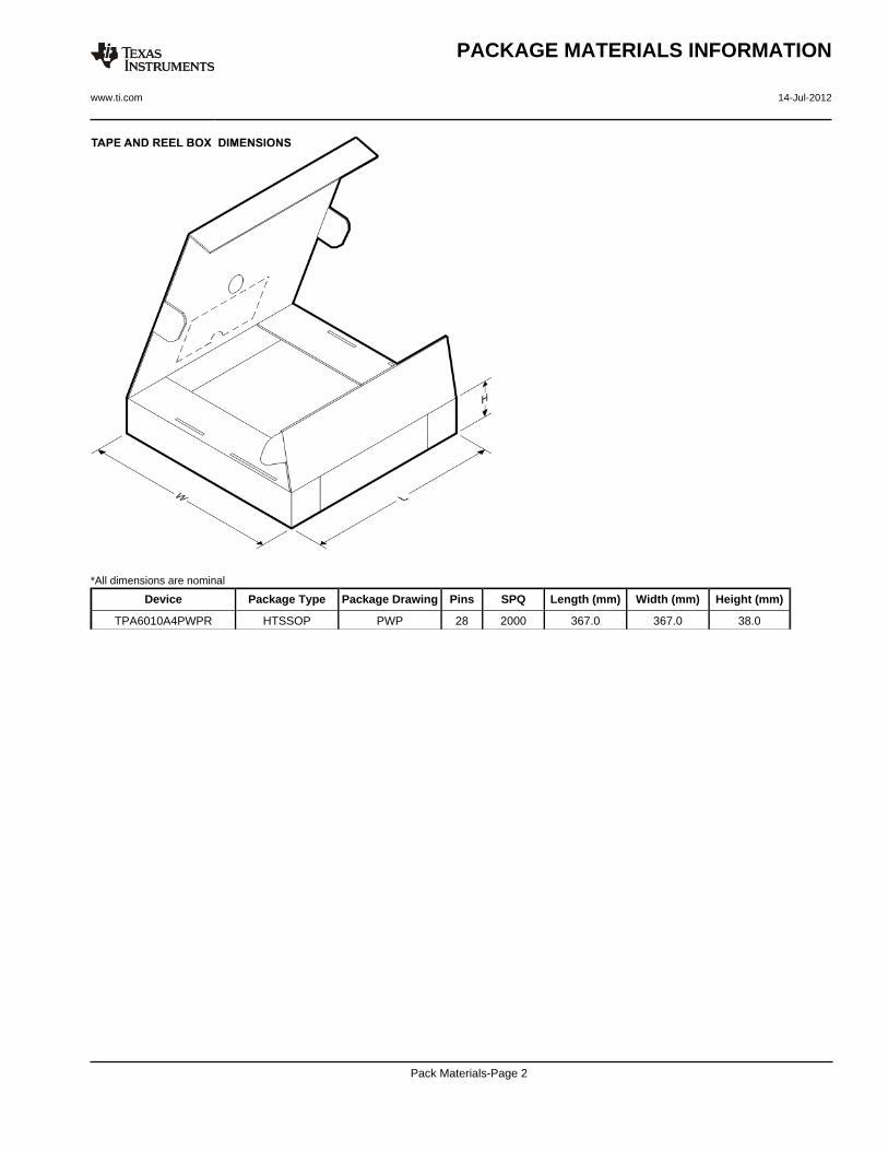
TPA6010A4PWPR HTSSOP PWP 28 2000 330.0 16.4 6.9 10.2 1.8 12.0 16.0 Q1
PACKAGE MATERIALS INFORMATION
www.ti.com 14-Jul-2012
Pack Materials-Page 1
*All dimensions are nominal
Device Package Type Package Drawing Pins SPQ Length (mm) Width (mm) Height (mm)
TPA6010A4PWPR HTSSOP PWP 28 2000 367.0 367.0 38.0
PACKAGE MATERIALS INFORMATION
www.ti.com 14-Jul-2012
Pack Materials-Page 2
IMPORTANT NOTICE
Texas Instruments Incorporated and its subsidiaries (TI) reserve the right to make corrections, enhancements, improvements and otherchanges to its semiconductor products and services per JESD46, latest issue, and to discontinue any product or service per JESD48, latestissue. Buyers should obtain the latest relevant information before placing orders and should verify that such information is current andcomplete. All semiconductor products (also referred to herein as “components”) are sold subject to TI’s terms and conditions of salesupplied at the time of order acknowledgment.TI warrants performance of its components to the specifications applicable at the time of sale, in accordance with the warranty in TI’s termsand conditions of sale of semiconductor products. Testing and other quality control techniques are used to the extent TI deems necessaryto support this warranty. Except where mandated by applicable law, testing of all parameters of each component is not necessarilyperformed.TI assumes no liability for applications assistance or the design of Buyers’ products. Buyers are responsible for their products andapplications using TI components. To minimize the risks associated with Buyers’ products and applications, Buyers should provideadequate design and operating safeguards.TI does not warrant or represent that any license, either express or implied, is granted under any patent right, copyright, mask work right, orother intellectual property right relating to any combination, machine, or process in which TI components or services are used. Informationpublished by TI regarding third-party products or services does not constitute a license to use such products or services or a warranty orendorsement thereof. Use of such information may require a license from a third party under the patents or other intellectual property of thethird party, or a license from TI under the patents or other intellectual property of TI.Reproduction of significant portions of TI information in TI data books or data sheets is permissible only if reproduction is without alterationand is accompanied by all associated warranties, conditions, limitations, and notices. TI is not responsible or liable for such altereddocumentation. Information of third parties may be subject to additional restrictions.Resale of TI components or services with statements different from or beyond the parameters stated by TI for that component or servicevoids all express and any implied warranties for the associated TI component or service and is an unfair and deceptive business practice.TI is not responsible or liable for any such statements.Buyer acknowledges and agrees that it is solely responsible for compliance with all legal, regulatory and safety-related requirementsconcerning its products, and any use of TI components in its applications, notwithstanding any applications-related information or supportthat may be provided by TI. Buyer represents and agrees that it has all the necessary expertise to create and implement safeguards whichanticipate dangerous consequences of failures, monitor failures and their consequences, lessen the likelihood of failures that might causeharm and take appropriate remedial actions. Buyer will fully indemnify TI and its representatives against any damages arising out of the useof any TI components in safety-critical applications.In some cases, TI components may be promoted specifically to facilitate safety-related applications. With such components, TI’s goal is tohelp enable customers to design and create their own end-product solutions that meet applicable functional safety standards andrequirements. Nonetheless, such components are subject to these terms.No TI components are authorized for use in FDA Class III (or similar life-critical medical equipment) unless authorized officers of the partieshave executed a special agreement specifically governing such use.Only those TI components which TI has specifically designated as military grade or “enhanced plastic” are designed and intended for use inmilitary/aerospace applications or environments. Buyer acknowledges and agrees that any military or aerospace use of TI componentswhich have not been so designated is solely at the Buyer's risk, and that Buyer is solely responsible for compliance with all legal andregulatory requirements in connection with such use.TI has specifically designated certain components as meeting ISO/TS16949 requirements, mainly for automotive use. In any case of use ofnon-designated products, TI will not be responsible for any failure to meet ISO/TS16949.
Products ApplicationsAudio www.ti.com/audio Automotive and Transportation www.ti.com/automotiveAmplifiers amplifier.ti.com Communications and Telecom www.ti.com/communicationsData Converters dataconverter.ti.com Computers and Peripherals www.ti.com/computersDLP® Products www.dlp.com Consumer Electronics www.ti.com/consumer-appsDSP dsp.ti.com Energy and Lighting www.ti.com/energyClocks and Timers www.ti.com/clocks Industrial www.ti.com/industrialInterface interface.ti.com Medical www.ti.com/medicalLogic logic.ti.com Security www.ti.com/securityPower Mgmt power.ti.com Space, Avionics and Defense www.ti.com/space-avionics-defenseMicrocontrollers microcontroller.ti.com Video and Imaging www.ti.com/videoRFID www.ti-rfid.comOMAP Applications Processors www.ti.com/omap TI E2E Community e2e.ti.comWireless Connectivity www.ti.com/wirelessconnectivity
Mailing Address: Texas Instruments, Post Office Box 655303, Dallas, Texas 75265Copyright © 2016, Texas Instruments Incorporated