Embed Size (px)
Citation preview

Power Supply
110VAC->240VAC
TAS5630
30V
TPA322x
Audio SourceAnd Control
RIGHT
LEFT
LC Filter
LC Filter
RESET
FAULT
HEAD
FREQ_ADJ
OSCM/P
OTW_CLIP
Modulation Mode Select
Switching Frequency Select
5V
Master/Slave Synchronization
Copyright © 2017, Texas Instruments Incorporated
CMUTE
PVDD
GVDD
AVDD
VDD
PBTL
Detect
Product
Folder
Order
Now
Technical
Documents
Tools &
Software
Support &Community
An IMPORTANT NOTICE at the end of this data sheet addresses availability, warranty, changes, use in safety-critical applications,intellectual property matters and other important disclaimers. PRODUCTION DATA.
TPA3221SLASEE9B –SEPTEMBER 2017–REVISED DECEMBER 2017
TPA3221 100-W Stereo, 200-W Mono HD-Audio, Analog-Input, Class-D Amplifier
1
1 Features1• Wide 7-V to 30-V Supply Voltage Operation• Stereo (2 x BTL) and Mono (1 x PBTL) Operation• Output Power at 10% THD+N
– 105-W Stereo into 4 Ω in BTL Configuration– 112-W Stereo into 3 Ω in BTL Configuration– 208-W Mono into 2 Ω in PBTL Configuration
• Output Power at 1% THD+N– 88-W Stereo into 4 Ω in BTL Configuration– 100-W Stereo into 3 Ω in BTL Configuration– 170-W Mono into 2 Ω in PBTL Configuration
• 5-V Gate Drive or Built-in LDO for Optional Single-Supply Operation
• Closed-Loop Feedback Design– Signal Bandwidth up to 100 kHz for High-
Frequency Content From HD Sources– 0.02% THD+N at 1 W into 4 Ω– 60-dB PSRR (BTL, No Input Signal)– <75-µV Output Noise (A-Weighted)– >108-dB SNR (A-Weighted)– AD or HEAD Modulation Schemes
• Low-Power Operating Modes– Standby Modes: Mute and < 1 mA Shutdown– Low Idle-Current HEAD Modulation Scheme– Single-Channel BTL Operation
• Multiple Input Options to Simplify Pre-Amp Design– Differential or Single-Ended Analog Inputs– Selectable Gains: 18 dB, 24 dB, 30 dB, 34 dB
• Integrated Protection: Undervoltage, Overvoltage,Cycle-by-cycle Current Limit, Short Circuit,Clipping Detection, Overtemperature Warning andShutdown, and DC Speaker Protection
• 90% Efficient Class-D Operation (4 Ω)• Pin-Compatible Family of Devices with Voltage
and Power-Level Options
2 Applications• Wireless and Powered Speakers• Soundbars• Subwoofers• Bookshelf Stereo Systems• Professional and Public Address (PA) Speakers
3 DescriptionTPA3221 is a high-power Class-D amplifier thatenables efficient operation at full-power, idle andstandby. The device features closed-loop feedbackwith a bandwidth up to 100 kHz, which provides lowdistortion across the audio band and deliversexcellent sound quality. The device operates witheither AD or low idle-current HEAD (High Efficient ADmode) modulation, and can drive up to 2 x 10⁵ W into4-Ω load or 1 x 208 W into 2-Ω load.
The TPA3221 features a single-ended or differentialanalog-input interface that supports up to 2 VRMS withfour selectable gains: 18 dB, 24 dB, 30 dB and 34dB. The TPA3221 also achieves >90% efficiency, lowidle power (<0.25 W) and ultra-low standby power(<0.1 W). This is made possible through the use of70-mΩ MOSFETs, an optimized gate drive schemeand low-power operating modes. TPA3221 includes abuilt-in LDO for easy integration in single-power-supply systems. To further simplify the design, thedevice integrates essential protection featuresincluding undervoltage, overvoltage, cycle-by-cyclecurrent limit, short circuit, clipping detection,overtemperature warning and shutdown, as well asDC speaker protection.
Device Information(1)
PART NUMBER PACKAGE BODY SIZE (NOM)TPA3221 HTSSOP (44) 6.10 mm x 14.00 mm
(1) For all available packages, see the orderable addendum atthe end of the datasheet.
Simplified Schematic

2
TPA3221SLASEE9B –SEPTEMBER 2017–REVISED DECEMBER 2017 www.ti.com
Product Folder Links: TPA3221
Submit Documentation Feedback Copyright © 2017, Texas Instruments Incorporated
Table of Contents1 Features .................................................................. 12 Applications ........................................................... 13 Description ............................................................. 14 Revision History..................................................... 25 Device Comparison Table ..................................... 36 Pin Configuration and Functions ......................... 37 Specifications......................................................... 5
7.1 Absolute Maximum Ratings ...................................... 57.2 ESD Ratings.............................................................. 57.3 Recommended Operating Conditions....................... 67.4 Thermal Information .................................................. 67.5 Electrical Characteristics........................................... 77.6 Audio Characteristics (BTL) ...................................... 97.7 Audio Characteristics (PBTL) ................................... 97.8 Typical Characteristics, BTL Configuration, AD-
mode ........................................................................ 107.9 Typical Characteristics, PBTL Configuration, AD-
mode ........................................................................ 138 Parameter Measurement Information ................ 159 Detailed Description ............................................ 15
9.1 Overview ................................................................. 15
9.2 Functional Block Diagrams ..................................... 169.3 Feature Description................................................. 189.4 Device Functional Modes........................................ 24
10 Application and Implementation........................ 3010.1 Application Information.......................................... 3010.2 Typical Applications .............................................. 30
11 Power Supply Recommendations ..................... 3411.1 Power Supplies ..................................................... 34
12 Layout................................................................... 3512.1 Layout Guidelines ................................................. 3512.2 Layout Examples................................................... 36
13 Device and Documentation Support ................. 3913.1 Documentation Support ........................................ 3913.2 Receiving Notification of Documentation Updates 3913.3 Community Resources.......................................... 3913.4 Trademarks ........................................................... 3913.5 Electrostatic Discharge Caution............................ 3913.6 Glossary ................................................................ 39
14 Mechanical, Packaging, and OrderableInformation ........................................................... 39
4 Revision History
Changes from Revision A (November 2017) to Revision B Page
• Changed OUT_P To: OUT1_P for 1 x BTL in Table 1 .......................................................................................................... 4• Added pins OSCM, OSCP to the Interface pins in the Absolute Maximun Ratings table...................................................... 5• Changed the TJ MIN value From: 0°C To –40°C in the Absolute Maximun Ratings table .................................................... 5• Deleted TJ Junction Temperature from the Recommended Operating Conditions table ....................................................... 5• Changed the capacitor on IN1_P, IN2_P and IN1_M, IN2_M From: 10µF To: 1µF in Figure 50 ........................................ 30• Changed the capacitor on IN1_P and IN1_M From: 10µF To: 1µF in Figure 51................................................................. 32• Changed the capacitor on IN1_P and IN1_M From: 10µF To: 1µF in Figure 52................................................................. 33
Changes from Original (September 2017) to Revision A Page
• Changed From: Advanced Information To: Production Data ................................................................................................. 1

13
14
15
16
17
18
1
2
3
45
67
89
10
11
12
19
202122
44
43
42
41
31
2728
29
30
32
33
34
35
36
40
3938
37
2526
23
24
GND
GAIN/SLV
FAULT
OTW_CLIP
AVDD
GND
CMUTE
IN2_M
OSCP
OSCM
GND
GND
IN2_P
GND
PVDD
GND
BST1_P
PVDD
GND
OUT1_M
BST1_M
GND
OUT2_P
PVDD
OUT1_P
PVDD
GND
BST2_P
BST2_M
OUT2_M
VDD
GVDD
GND
GND
OUT2_M
OUT1_P
PVDD
PVDD
GND
HEAD
FREQ_ADJ
IN1_P
IN1_M
RESET
3
TPA3221www.ti.com SLASEE9B –SEPTEMBER 2017–REVISED DECEMBER 2017
Product Folder Links: TPA3221
Submit Documentation FeedbackCopyright © 2017, Texas Instruments Incorporated
5 Device Comparison Table
DEVICE NAME DESCRIPTION THERMAL PADLOCATION
TPA3221PIN-COMPATIBLE
TPA3220 35 W Stereo, 100 W Peak HD-Audio, Analog-Input, Class-D Amplifier Bottom YTPA3244 40 W Stereo, 100 W Peak Ultra-HD, Analog-Input Class-D Amplifier BottomTPA3245 100 W Stereo, 200 W Mono Ultra-HD, Analog-Input Class-D Amplifier TopTPA3250 70 W Stereo, 130 W Peak Ultra-HD, Analog-Input Class-D Amplifier BottomTPA3251 175 W Stereo, 350 W Mono Ultra-HD, Analog-Input Class-D Amplifier TopTPA3255 315 W Stereo, 600 W Mono Ultra-HD, Analog-Input Class-D Amplifier Top
6 Pin Configuration and FunctionsThe TPA3221 is available in a thermally enhanced TSSOP package.
The package type contains a heat slug that is located on the top side of the device for convenient thermalcoupling to the heat sink.
DDV PackageHTSSOP 44-Pin
(Top View)

4
TPA3221SLASEE9B –SEPTEMBER 2017–REVISED DECEMBER 2017 www.ti.com
Product Folder Links: TPA3221
Submit Documentation Feedback Copyright © 2017, Texas Instruments Incorporated
Pin FunctionsNAME NO. I/O DESCRIPTION
HEAD 11 I 0 = AD, 1 = HEAD. Refer to: AD-Mode and HEAD-Mode PWM Modulation
AVDD 21 P AVDD voltage supply. Refer to: Internal LDO, AVDD and GVDD Supplies
BST1_M 43 P OUT1_M HS bootstrap supply (BST), 0.033 μF capacitor to OUT1_M required.Refer to: BST capacitors
BST1_P 44 P OUT1_P HS bootstrap supply (BST), 0.033 μF capacitor to OUT1_P required.Refer to: BST capacitors
BST2_M 23 P OUT2_M HS bootstrap supply (BST), 0.033 μF capacitor to OUT2_M required.Refer to: BST capacitors
BST2_P 24 P OUT2_P HS bootstrap supply (BST), 0.033 μF capacitor to OUT2_P required.Refer to: BST capacitors
CMUTE 17 P Mute and Startup Timing Capacitor. Connect a 33 nF capacitor to GND. Refer to: Device Reset
FAULT 4 O Shutdown signal, open drain; active low. Refer to: Error Reporting
FREQ_ADJ 14 O Oscillator frequency programming pin. Refer to: Oscillator
GAIN/SLV 2 I Closed loop gain and master/slave programming pin.Refer to: Input Configuration, Gain Setting And Master / Slave Operation
GND 5, 6, 7, 18, 19, 20, 25, 26, 33,34, 41, 42
P Ground
GVDD 22 P Gate drive supply. Refer to: Internal LDO, AVDD and GVDD Supplies
IN1_M 9 I Negative audio input for channel 1
IN1_P 8 I Positive audio input for channel 1
IN2_M 16 I Negative audio input for channel 2
IN2_P 15 I Positive audio input for channel 2
OSCM 12 I/O Oscillator synchronization interface.Refer to: Input Configuration, Gain Setting And Master / Slave Operation
OSCP 13 I/O Oscillator synchronization interface.Refer to: Input Configuration, Gain Setting And Master / Slave Operation
OTW_CLIP 3 O Clipping warning and Over-temperature warning; open drain; active low.Refer to: Error Reporting
OUT1_M 35 O Negative output for channel 1
OUT1_P 39, 40 O Positive output for channel 1
OUT2_M 27, 28 O Negative output for channel 2
OUT2_P 32 O Positive output for channel 2
PVDD 29, 30, 31, 36, 37, 38 P PVDD supply. Refer to: PVDD Capacitor Recommendation, PVDD Supply
RESET 10 I Device reset Input; active low. Refer to: Fault Handling, Powering Up, Powering Down
VDD 1 P Input power supply. Refer to: Internal LDO, VDD Supply
PowerPad™ P Ground, connect to grounded heatsink. Placed on top side of device.
(1) X refers to inputs connected through AC coupling capacitor, 0 refers to logic low (GND), 1 refers to logic high (AVDD).(2) 2N refers to differential input signal, 1N refers to single ended input signal. +1 refers to number of logic control (RESET) input pins.
Table 1. Mode Selection PinsMODE PINS (1)
INPUT MODE (2) OUTPUTCONFIGURATION DESCRIPTION
IN2_M IN2_P HEADX X 0 1N/2N + 1 2 × BTL Stereo, BTL output configuration, AD mode modulationX X 1 1N/2N + 1 2 × BTL Stereo, BTL output configuration, HEAD mode modulation
0 0 0 1N/2N + 1 1 x PBTL Mono, Parallelled BTL configuration. Connect OUT1_P to OUT2_Pand OUT1_M to OUT2_M, AD mode modulation
0 0 1 1N/2N + 1 1 x PBTL Mono, Parallelled BTL configuration. Connect OUT1_P to OUT2_Pand OUT1_M to OUT2_M, HEAD mode modulation
1 1 0 1N/2N + 1 1 x BTL Mono, BTL configuration. OUT1_M and OUT1_P active, AD modemodulation
1 1 1 1N/2N + 1 1 x BTL Mono, BTL configuration. OUT1_M and OUT1_P active, HEAD modemodulation

5
TPA3221www.ti.com SLASEE9B –SEPTEMBER 2017–REVISED DECEMBER 2017
Product Folder Links: TPA3221
Submit Documentation FeedbackCopyright © 2017, Texas Instruments Incorporated
(1) Stresses beyond those listed under Absolute Maximum Ratings may cause permanent damage to the device. These are stress ratingsonly, which do not imply functional operation of the device at these or any other conditions beyond those indicated under RecommendedOperating Conditions. Exposure to absolute-maximum-rated conditions for extended periods may affect device reliability.
(2) These voltages represents the DC voltage + peak AC waveform measured at the terminal of the device in all conditions.
7 Specifications
7.1 Absolute Maximum RatingsOver operating free-air temperature range (unless otherwise noted) (1)
MIN MAX UNIT
Supply voltage
PVDD to GND (2) –0.3 37 VBST_X to GVDD (2) –0.3 37 VBST1_M, BST1_P, BST2_M, BST2_P to GND (2) –0.3 47.8 VVDD to GND –0.3 43 VGVDD to GND (2) –0.3 5.5 VAVDD to GND –0.3 5.5 V
Interface pins
OUT1_M, OUT1_P, OUT2_M, OUT2_P to GND (2) –0.3 43 VIN1_M, IN1_P, IN2_M, IN2_P to GND –0.3 5.5 VHEAD, FREQ_ADJ, GAIN/SLV, CMUTE, RESET, OSCP, OSCM to GND –0.3 5.5 VFAULT, OTW_CLIP to GND –0.3 5.5 VContinuous sink current, FAULT, OTW_CLIP to GND 9 mA
TJ Operating junction temperature range –40 150 °CTstg Storage temperature range –40 150 °C
(1) JEDEC document JEP155 states that 500-V HBM allows safe manufacturing with a standard ESD control process.(2) JEDEC document JEP157 states that 250-V CDM allows safe manufacturing with a standard ESD control process.
7.2 ESD RatingsVALUE UNIT
VESD Electrostatic discharge
Human body model (HBM), per ANSI/ESDA/JEDEC JS-001, allpins (1) ±1000 V
Charged device model (CDM), per JEDEC specificationJESD22-C101, all pins (2) ±250 V

6
TPA3221SLASEE9B –SEPTEMBER 2017–REVISED DECEMBER 2017 www.ti.com
Product Folder Links: TPA3221
Submit Documentation Feedback Copyright © 2017, Texas Instruments Incorporated
(1) VDD must be connected to a supply of 5V in LDO bypass mode; OR 7V to 30V with LDO active. VDD can be connected directly toPVDD in LDO bypass mode, but must not exceed PVDD voltage.
7.3 Recommended Operating Conditionsover operating free-air temperature range (unless otherwise noted)
MIN TYP MAX UNITPVDD Power-stage supply DC supply voltage 7 30 32 V
VDD (1)
Supply voltage for internal LDO regulatorto supply GVDD and AVDD DC supply voltage 7 32 V
External supply for VDD, GVDD andAVDD. Internal LDO bypassed DC supply voltage 4.5 5 5.5 V
AVDD Supply voltage for analog circuits DC supply voltage 4.5 5 5.5 VGVDD Supply voltage for gate-drive circuitry DC supply voltage 4.5 5 5.5 VLOUT(BTL) Output filter inductance Minimum output inductance at IOC 5 10
μHLOUT(PBTL)
Output filter inductance, PBTL before theLC filter Minimum output inductance at IOC 5 10
Output filter inductance, PBTL after theLC filter
Minimum output inductance at half IOC ,each inductor 5 10
FPWM
PWM frame rate selectable for AMinterference avoidance; 1% Resistortolerance
Nominal 575 600 625kHzAM1 510 533 555
AM2 460 480 500
R(FREQ_ADJ) PWM frame rate programming resistorNominal; Master mode 49.5 50 50.5
kΩAM1; Master mode 29.7 30 30.3AM2; Master mode 9.9 10 10.1
CPVDD PVDD close decoupling capacitors 1.0 μF
V(FREQ_ADJ)Voltage on FREQ_ADJ pin for slavemode operation Slave Mode (Connect to AVDD) 5 V
(1) For more information about traditional and new thermal metrics, see the Semiconductor and IC Package Thermal Metrics applicationreport.
(2) Thermal data are obtained with 85°C heat sink temperature using thermal compound with 0.7W/mK thermal conductivity and 2milthickness. In this model heat sink temperature is considered to be the ambient temperature and only path for dissipation is to theheatsink.
7.4 Thermal Information
THERMAL METRIC (1)
TPA3221
UNITDDV 44-PINS HTSSOP
JEDEC STANDARD 4 LAYERPCB
FIXED 85°CHEATSINK
TEMPERATURE (2)
RθJA Junction-to-ambient thermal resistance 44.8 5.5 °C/WRθJC(top) Junction-to-case (top) thermal resistance 1.1 2.0 °C/WRθJB Junction-to-board thermal resistance 14.9 n/a °C/WψJT Junction-to-top characterization parameter 0.6 n/a °C/WψJB Junction-to-board characterization parameter 14.7 n/a °C/WRθJC(bot) Junction-to-case (bottom) thermal resistance n/a n/a °C/W
7
TPA3221www.ti.com SLASEE9B –SEPTEMBER 2017–REVISED DECEMBER 2017
Product Folder Links: TPA3221
Submit Documentation FeedbackCopyright © 2017, Texas Instruments Incorporated
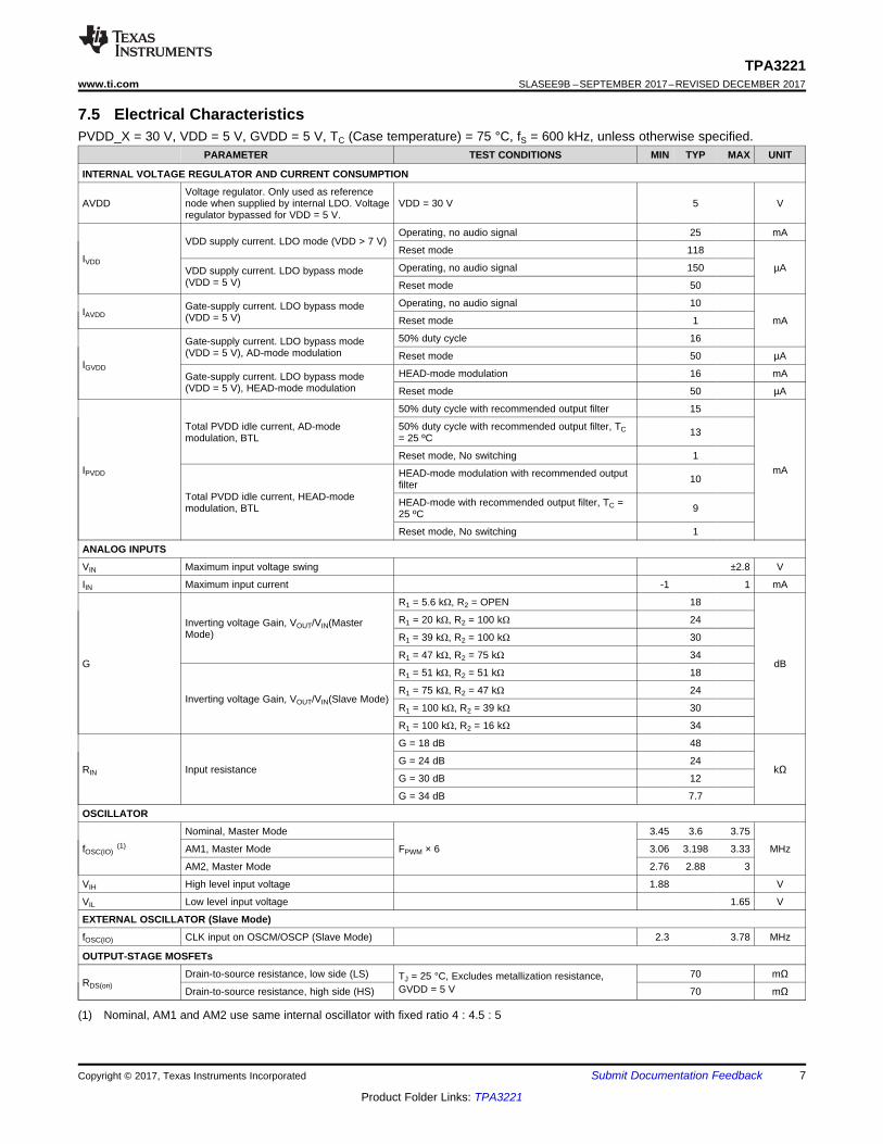
(1) Nominal, AM1 and AM2 use same internal oscillator with fixed ratio 4 : 4.5 : 5
7.5 Electrical CharacteristicsPVDD_X = 30 V, VDD = 5 V, GVDD = 5 V, TC (Case temperature) = 75 °C, fS = 600 kHz, unless otherwise specified.
PARAMETER TEST CONDITIONS MIN TYP MAX UNIT
INTERNAL VOLTAGE REGULATOR AND CURRENT CONSUMPTION
AVDDVoltage regulator. Only used as referencenode when supplied by internal LDO. Voltageregulator bypassed for VDD = 5 V.
VDD = 30 V 5 V
IVDD
VDD supply current. LDO mode (VDD > 7 V)Operating, no audio signal 25 mA
Reset mode 118
µAVDD supply current. LDO bypass mode(VDD = 5 V)
Operating, no audio signal 150
Reset mode 50
IAVDDGate-supply current. LDO bypass mode(VDD = 5 V)
Operating, no audio signal 10
mAReset mode 1
IGVDD
Gate-supply current. LDO bypass mode(VDD = 5 V), AD-mode modulation
50% duty cycle 16
Reset mode 50 µA
Gate-supply current. LDO bypass mode(VDD = 5 V), HEAD-mode modulation
HEAD-mode modulation 16 mA
Reset mode 50 µA
IPVDD
Total PVDD idle current, AD-modemodulation, BTL
50% duty cycle with recommended output filter 15
mA
50% duty cycle with recommended output filter, TC= 25 ºC 13
Reset mode, No switching 1
Total PVDD idle current, HEAD-modemodulation, BTL
HEAD-mode modulation with recommended outputfilter 10
HEAD-mode with recommended output filter, TC =25 ºC 9
Reset mode, No switching 1
ANALOG INPUTS
VIN Maximum input voltage swing ±2.8 V
IIN Maximum input current -1 1 mA
G
Inverting voltage Gain, VOUT/VIN(MasterMode)
R1 = 5.6 kΩ, R2 = OPEN 18
dB
R1 = 20 kΩ, R2 = 100 kΩ 24
R1 = 39 kΩ, R2 = 100 kΩ 30
R1 = 47 kΩ, R2 = 75 kΩ 34
Inverting voltage Gain, VOUT/VIN(Slave Mode)
R1 = 51 kΩ, R2 = 51 kΩ 18
R1 = 75 kΩ, R2 = 47 kΩ 24
R1 = 100 kΩ, R2 = 39 kΩ 30
R1 = 100 kΩ, R2 = 16 kΩ 34
RIN Input resistance
G = 18 dB 48
kΩG = 24 dB 24
G = 30 dB 12
G = 34 dB 7.7
OSCILLATOR
fOSC(IO)(1)
Nominal, Master Mode
FPWM × 6
3.45 3.6 3.75
MHzAM1, Master Mode 3.06 3.198 3.33
AM2, Master Mode 2.76 2.88 3
VIH High level input voltage 1.88 V
VIL Low level input voltage 1.65 V
EXTERNAL OSCILLATOR (Slave Mode)
fOSC(IO) CLK input on OSCM/OSCP (Slave Mode) 2.3 3.78 MHz
OUTPUT-STAGE MOSFETs
RDS(on)Drain-to-source resistance, low side (LS) TJ = 25 °C, Excludes metallization resistance,
GVDD = 5 V70 mΩ
Drain-to-source resistance, high side (HS) 70 mΩ

8
TPA3221SLASEE9B –SEPTEMBER 2017–REVISED DECEMBER 2017 www.ti.com
Product Folder Links: TPA3221
Submit Documentation Feedback Copyright © 2017, Texas Instruments Incorporated
Electrical Characteristics (continued)PVDD_X = 30 V, VDD = 5 V, GVDD = 5 V, TC (Case temperature) = 75 °C, fS = 600 kHz, unless otherwise specified.
PARAMETER TEST CONDITIONS MIN TYP MAX UNIT
(2) Specified by design.
I/O PROTECTION
Vuvp,AVDD Undervoltage protection limit, AVDD 4 V
Vuvp,AVDD,hyst(2) Undervoltage protection hysteresis, AVDD 0.1 V
Vuvp,PVDD Undervoltage protection limit, PVDD_x 6.4 V
Vuvp,PVDD,hyst(2) Undervoltage protection hysteresis, PVDD_x 0.45 V
Vovp,PVDD Overvoltage protection limit, PVDD_x 34 V
Vovp,PVDD,hyst(2) Overvoltage protection hysteresis, PVDD_x 0.45 V
OTW Overtemperature warning, OTW_CLIP (2) 115 125 135 °C
OTWhyst(2)
Temperature drop needed below OTWtemperature for OTW_CLIP to be inactiveafter OTW event.
20 °C
OTE (2) Overtemperature error 145 155 165 °C
OTEhyst(2) A reset needs to occur for FAULT to be
released following an OTE event 20 °C
OTE-OTW(differential)(2) OTE-OTW differential 25 °C
OLPC Overload protection counter fPWM = 600 kHz (1024 PWM cycles) 1.7 ms
IOC, BTL Overcurrent limit protection, speaker outputcurrent Nominal peak current in 1Ω load
10 A
IOC, PBTL 20 A
IDCspkr, BTLDC Speaker Protection Current Threshold
BTL current imbalance threshold 1.8 A
IDCspkr, PBTL PBTL current imbalance threshold 3.6 A
IOCT Overcurrent response time Time from switching transition to flip-state inducedby overcurrent. 150 ns
IPD Output pulldown current of each half Connected when RESET is active to providebootstrap charge. Not used in SE mode. 3 mA
STATIC DIGITAL SPECIFICATIONS
VIH High level input voltage
HEAD, OSCM, OSCP,CMUTE, RESET
1.9 V
VIL Low level input voltage 0.8 V
Ilkg Input leakage current 100 μA
OTW/SHUTDOWN (FAULT)
RINT_PUInternal pullup resistance, OTW_CLIP toAVDD, FAULT to AVDD 20 26 32 kΩ
VOH High level output voltage Internal pullup resistor 3 3.3 3.6 V
VOL Low level output voltage IO = 4 mA 200 500 mV
Device fanout OTW_CLIP, FAULT No external pullup 30 devices

9
TPA3221www.ti.com SLASEE9B –SEPTEMBER 2017–REVISED DECEMBER 2017
Product Folder Links: TPA3221
Submit Documentation FeedbackCopyright © 2017, Texas Instruments Incorporated
(1) SNR is calculated relative to 1% THD+N output level.(2) Actual system idle losses also are affected by core losses of output inductors.
7.6 Audio Characteristics (BTL)PCB and system configuration are in accordance with recommended guidelines. Audio frequency = 1 kHz, PVDD_X = 30 V,VDD = 5 V, GVDD = 5 V, RL = 4 Ω, fS = 600 kHz, TC = 75°C, Output Filter: LDEM = 10 μH, CDEM = 1 µF, AD-Modulation,AES17 + AUX-0025 measurement filters, unless otherwise noted.
PARAMETER TEST CONDITIONS MIN TYP MAX UNIT
PO Power output per channel
RL = 3 Ω, 10% THD+N 112
WRL = 4 Ω, 10% THD+N 105RL = 3 Ω, 1% THD+N 100RL = 4 Ω, 1% THD+N 88
THD+N Total harmonic distortion + noise 1 W 0.02 %
Vn Output integrated noise A-weighted, AES17 filter, Input CapacitorGrounded, Gain = 18 dB 75 μV
|VOS| Output offset voltage Inputs AC coupled to GND 20 60 mVSNR Signal-to-noise ratio (1) A-weighted, Gain = 18 dB 108 dBDNR Dynamic range A-weighted, Gain = 18 dB 109 dB
Pidle Power dissipation due to idle losses (IPVDD_X)
PO = 0, all outputs switching, AD-modulation,TC = 25°C (2) 0.37 W
PO = 0, all outputs switching, HEAD-modulation, TC = 25°C (2) 0.25 W
(1) SNR is calculated relative to 1% THD+N output level.(2) Actual system idle losses are affected by core losses of output inductors.
7.7 Audio Characteristics (PBTL)PCB and system configuration are in accordance with recommended guidelines. Audio frequency = 1 kHz, PVDD_X = 30 V,VDD = 5 V, GVDD = 5 V, RL = 2 Ω, fS = 600 kHz, TC = 75°C, Output Filter: LDEM = 10 μH, CDEM = 1 µF, Pre-Filter PBTL, AD-Modulation, AES17 + AUX-0025 measurement filters, unless otherwise noted.
PARAMETER TEST CONDITIONS MIN TYP MAX UNIT
PO Power output per channel
RL = 2 Ω, 10% THD+N 208
W
RL = 3 Ω, 10% THD+N 155RL = 4 Ω, 10% THD+N 120RL = 2 Ω, 1% THD+N 170RL = 3 Ω, 1% THD+N 125RL = 4 Ω, 1% THD+N 98
THD+N Total harmonic distortion + noise 1 W 0.02 %
Vn Output integrated noise A-weighted, AES17 filter, Input CapacitorGrounded, Gain = 18 dB 75 μV
|VOS| Output offset voltage Inputs AC coupled to GND 20 60 mVSNR Signal to noise ratio (1) A-weighted, Gain = 18 dB 108 dBDNR Dynamic range A-weighted, Gain = 18 dB 110 dB
Pidle Power dissipation due to idle losses (IPVDD_X)
PO = 0, all outputs switching, AD-modulation, TC = 25°C (2) 0.20 W
PO = 0, all outputs switching, HEAD-modulation, TC = 25°C (2) 0.17 W

PVDD - Supply Voltage - V
PO
- O
utpu
t Pow
er -
W
5 10 15 20 25 30 350
20
40
60
80
100
120
D005
THD+N = 1%TC = 75qC
D005
3:3: - CB3C Limited4:8:
2 Channel Output Power - W
Effi
cien
cy -
%
1
10
100
10m 100m 1 10 100 300
D006
TC = 75qCPVDD = 30V
D006
3:4:8:
f - Frequency - Hz
TH
D+
N -
Tot
al H
arm
onic
Dis
tort
ion
+ N
oise
- %
0.001
0.01
0.1
1
10
20 40k100 1k 10k
D003
AUX-0025 Filter80 kHz analyzer BWRL = 4:, TC = 75qC
D003
1W10W50W
PVDD - Supply Voltage - V
PO
- O
utpu
t Pow
er -
W
5 10 15 20 25 30 350
20
40
60
80
100
120
D004
THD+N = 10%TC = 75qC
D004
3:3: - CB3C Limited4:8:
f - Frequency - Hz
TH
D+
N -
Tot
al H
arm
onic
Dis
tort
ion
+ N
oise
- %
0.00050.001
0.01
0.1
1
10
20 20k100 1k 10k
D002
RL = 4:TC = 75qC
D002
1W10W50W
Po - Output Power - W
TH
D+
N -
Tot
al H
arm
onic
Dis
tort
ion
+ N
oise
- %
0.001
0.01
0.1
1
10
10m 100m 1 10 100 200
D001
TC = 75qC
D001
3:4:8:
10
TPA3221SLASEE9B –SEPTEMBER 2017–REVISED DECEMBER 2017 www.ti.com
Product Folder Links: TPA3221
Submit Documentation Feedback Copyright © 2017, Texas Instruments Incorporated
7.8 Typical Characteristics, BTL Configuration, AD-modeAll Measurements taken at audio frequency = 1 kHz, PVDD_X = 30 V, VDD = 5 V, GVDD = 5 V, RL = 4 Ω, fS =600 kHz, 18 dB, TC = 75°C, Output Filter: LDEM = 10 μH, CDEM = 1 µF, AD-Modulation, AES17 + AUX-0025measurement filters, unless otherwise noted.
Figure 1. Total Harmonic Distortion + Noise vs OutputPower, AD-mode
Figure 2. Total Harmonic Distortion+Noise vs Frequency,AD-mode
Figure 3. Total Harmonic Distortion+Noise vs Frequency,AD-mode
Figure 4. Output Power vs Supply Voltage, AD-mode
Figure 5. Output Power vs Supply Voltage, AD-mode Figure 6. System Efficiency vs Output Power, AD-mode

f - Frequency - Hz
Noi
se A
mpl
itude
- d
B
-160
-140
-120
-100
-80
-60
-40
-20
0
5k 10k 20k0 25k 30k15k 35k 40k 45k48k
D011
TC = 75qCVref = 21.21 VFFT size = 16384AUX-0025 filter80kHz Analyzer BW
D011
4:
f - Frequency - Hz
18kH
z +
19k
Hz
1:1
-140
-120
-100
-80
-60
-40
-20
0
5k 10k 20k0 25k 30k15k 35k 40k
D012
TC = 75qCPout = 1W/channel FFT size = 16384
AUX-0025 filter80kHz Analyzer BW
D012
4:
2 Channel Output Power - W
Pow
er L
oss
- W
0 25 50 75 100 125 150 175 200 225 2500
25
50
75
D009
TC = 75qCPVDD = 30V
D009
3:4:8:
TC - Case Temperature - qC
PO
- O
utpu
t Pow
er -
W
0 25 50 75 1000
25
50
75
100
125
150
D010
THD+N = 10%
D010
3:4:8:
2 Channel Output Power - W
Effi
cien
cy -
%
1
10
100
10m 100m 1 10 100 200
D007
TC = 75qCPVDD = 24V
D007
3:4:8:
2 Channel Output Power - W
Effi
cien
cy -
%
1
10
100
10m 100m 1 10 50
D008
TC = 75qCPVDD = 12V
D008
3:4:8:
11
TPA3221www.ti.com SLASEE9B –SEPTEMBER 2017–REVISED DECEMBER 2017
Product Folder Links: TPA3221
Submit Documentation FeedbackCopyright © 2017, Texas Instruments Incorporated
Typical Characteristics, BTL Configuration, AD-mode (continued)
Figure 7. System Efficiency vs Output Power, AD-mode Figure 8. System Efficiency vs Output Power, AD-mode
Figure 9. System Power Loss vs Output Power, AD-mode Figure 10. Output Power vs Case Temperature, AD-mode
Figure 11. Noise Amplitude vs Frequency, AD-mode
18 kHz + 19 kHz Ratio 1 : 1
Figure 12. CCIF Intermodulation, AD-mode

PVDD - Supply Voltage - V
I PV
DD -
PV
DD
Idle
Cur
rent
- m
A
5 10 15 20 25 30 350
5
10
15
D026
RL = 4:TC = 25qC
D026
AD ModeHEAD Mode
f - Frequency - Hz
Cro
ssta
lk -
dB
r
-120
-100
-80
-60
-40
-20
0
10k 20k1k10020
D015
RL = 4:, TC = 75qCAggressor Amplitude = 2VRMS (1W)
D015
CH2 to CH1CH1 to CH2
f - Frequency - Hz
18kH
z +
19k
Hz
1:1
-140
-120
-100
-80
-60
-40
-20
0
5k 10k 20k0 30k15k 35k 40k25k
D013
TC = 75qCPout = 25W/channel FFT size = 16384
AUX-0025 filter80kHz Analyzer BW
D013
4:
f - Frequency - Hz
PS
RR
- d
B
-120
-100
-80
-60
-40
-20
0
10k 20k1k10020
D014
TC = 75qCPSU Ripple - 250mVp-p
D014
CH1CH2
12
TPA3221SLASEE9B –SEPTEMBER 2017–REVISED DECEMBER 2017 www.ti.com
Product Folder Links: TPA3221
Submit Documentation Feedback Copyright © 2017, Texas Instruments Incorporated
Typical Characteristics, BTL Configuration, AD-mode (continued)
18 kHz + 19 kHz Ratio 1 : 1
Figure 13. CCIF Intermodulation, AD-mode Figure 14. Power Supply Rejection Ratio vs Frequency, AD-mode
Figure 15. Channel to Channel Crosstalk vs Frequency, AD-mode Figure 16. Idle Current vs Supply Voltage

PVDD - Supply Voltage - V
PO
- O
utpu
t Pow
er -
W
5 10 15 20 25 30 350
25
50
75
100
125
150
175
200
D020
THD+N = 1%TC = 75qC
D020
2:3:4:
2 Channel Output Power - W
Effi
cien
cy -
%
1
10
100
10m 100m 1 10 100 300
D021
TC = 75qCPVDD = 30V
D021
2:3:4:
f - Frequency - Hz
TH
D+
N -
Tot
al H
arm
onic
Dis
tort
ion
+ N
oise
- %
0.001
0.01
0.1
1
10
20 40k100 1k 10k
D018
AUX-0025 Filter80 kHz analyzer BWRL = 2:, TC = 75qC
D018
1W25W100W
PVDD - Supply Voltage - V
PO
- O
utpu
t Pow
er -
W
5 10 15 20 25 30 350
25
50
75
100
125
150
175
200
225
D019
THD+N = 10%TC = 75qC
D019
2:2: - CB3C Limited3:4:
Po - Output Power - W
TH
D+
N -
Tot
al H
arm
onic
Dis
tort
ion
+ N
oise
- %
0.001
0.01
0.1
1
10
10m 100m 1 10 100 300
D016
TC = 75qC
D016
2:3:4:
f - Frequency - Hz
TH
D+
N -
Tot
al H
arm
onic
Dis
tort
ion
+ N
oise
- %
0.00050.001
0.01
0.1
1
10
20 20k100 1k 10k
D017
RL = 2:TC = 75qC
D017
1W25W100W
13
TPA3221www.ti.com SLASEE9B –SEPTEMBER 2017–REVISED DECEMBER 2017
Product Folder Links: TPA3221
Submit Documentation FeedbackCopyright © 2017, Texas Instruments Incorporated
7.9 Typical Characteristics, PBTL Configuration, AD-modeAll Measurements taken at audio frequency = 1 kHz, PVDD_X = 30 V, VDD = 5 V, GVDD = 5 V, RL = 2 Ω, fS =600 kHz, 18 dB, TC = 75°C, Output Filter: LDEM = 10 μH, CDEM = 1 µF, Pre-Filter PBTL, AD Modulation, AES17 +AUX-0025 measurement filters, unless otherwise noted.
Figure 17. Total Harmonic Distortion+Noise vs OutputPower, AD-mode
Figure 18. Total Harmonic Distortion + Noise vs Frequency,AD-mode
Figure 19. Total Harmonic Distortion+Noise vs Frequency,AD-mode
Figure 20. Output Power vs Supply Voltage, AD-mode
Figure 21. Output Power vs Supply Voltage, AD-mode Figure 22. System Efficiency vs Output Power, AD-mode

f - Frequency - Hz
18kH
z +
19k
Hz
1:1
-140
-120
-100
-80
-60
-40
-20
0
5k 10k 20k0 25k 30k15k 35k 40k
D024
TC = 75qCPout = 1W/channel FFT size = 16384
AUX-0025 filter80kHz Analyzer BW
D024
2:
f - Frequency - Hz
18kH
z +
19k
Hz
1:1
-140
-120
-100
-80
-60
-40
-20
0
5k 10k 20k0 25k 30k15k 35k 40k
D025
TC = 75qCPout = 50W/channel FFT size = 16384
AUX-0025 filter80kHz Analyzer BW
D025
2:
2 Channel Output Power - W
Pow
er L
oss
- W
0 25 50 75 100 125 150 175 200 2250
10
20
30
40
D022
TC = 75qCPVDD = 30V
D022
2:3:4:
TC - Case Temperature - qC
PO
- O
utpu
t Pow
er -
W
0 25 50 75 1000
50
100
150
200
250
D023
THD+N = 10%
D023
2:3:4:
14
TPA3221SLASEE9B –SEPTEMBER 2017–REVISED DECEMBER 2017 www.ti.com
Product Folder Links: TPA3221
Submit Documentation Feedback Copyright © 2017, Texas Instruments Incorporated
Typical Characteristics, PBTL Configuration, AD-mode (continued)
Figure 23. System Power Loss vs Output Power, AD-mode Figure 24. Output Power vs Case Temperature, AD-mode
18 kHz + 19 kHz Ratio 1 : 1
Figure 25. CCIF Intermodulation vs Frequency, AD-mode
18 kHz + 19 kHz Ratio 1 : 1
Figure 26. CCIF Intermodulation vs Frequency, AD-mode

15
TPA3221www.ti.com SLASEE9B –SEPTEMBER 2017–REVISED DECEMBER 2017
Product Folder Links: TPA3221
Submit Documentation FeedbackCopyright © 2017, Texas Instruments Incorporated
8 Parameter Measurement InformationAll parameters are measured according to the conditions described in the Recommended Operating Conditions.
Most audio analyzers will not give correct readings of Class-D amplifiers’ performance due to their sensitivity toout of band noise present at the amplifier output. AES-17 + AUX-0025 pre-analyzer filters are recommended touse for Class-D amplifier measurements. In absence of such filters, a 30-kHz low-pass filter (10 Ω + 47 nF) canbe used to reduce the out of band noise remaining on the amplifier outputs.
9 Detailed Description
9.1 OverviewTPA3221 is designed as a feature-enhanced cost efficient high power Class-D audio amplifier. It has built-inadvanced protection circuitry to ensure maximum product robustness as well as a flexible feature set includingbuilt in LDO for easy supply of low voltage circuitry, selectable gain, switching frequency, master/slavesynchronization of multiple devices, selectable PWM modulation scheme, mute function, temperature andclipping status signals. TPA3221 has a bandwidth up to 100 kHz and low output noise designed for highresolution audio applications and accepts both differential and single ended analog audio inputs at levels from 1VRMS to 2 VRMS. With its closed loop operation TPA3221 is designed for high audio performance with a systempower supply between 7 V and 30 V.
To facilitate system design, the TPA3221 needs only a (typical) 30 V power stage supply. The TPA3221 has aninternal voltage regulator supplied from the VDD pin for the analog and digital system blocks and the outputstage gate drive respectively. The VDD pin can be connected directly to PVDD in case of only this power supplyrail available.
To reduce device power losses external 5 V supplies can be used for the AVDD and VDD supply pins. Theinternal voltage regulator connected to the VDD pin is automatically turned off if using external 5 V supply for thispin. Although supplied from the same 5 V source, separating AVDD and VDD on the printed-circuit board (PCB)by RC filters (see application diagram for details) is recommended. These RC filters provide the recommendedhigh-frequency isolation. Special attention should be paid to placing all decoupling capacitors as close to theirassociated pins as possible. In general, the physical loop with the power supply pins, decoupling capacitors andGND return path to the device pins must be kept as short as possible and with as little area as possible tominimize induction (see Layout Examples for additional information).
The floating supplies for the output stage high side gate drives are supplied by built-in bootstrap circuitryrequiring only an external capacitor for each half-bridge.
For a properly functioning bootstrap circuit, a small ceramic capacitor must be connected from each bootstrap pin(BST_X) to the power-stage output pin (OUT_X). When the power-stage output is low, the bootstrap capacitor ischarged through an internal diode connected between the gate-drive power-supply pin (GVDD) and the bootstrappins. When the power-stage output is high, the bootstrap capacitor potential is shifted above the output potentialand thus provides a suitable voltage supply for the high-side gate driver. It is recommended to use 33 nF ceramiccapacitors, size 0603 or 0805, for the bootstrap supply. These 33 nF capacitors ensure sufficient energy storage,even during minimal PWM duty cycles, to keep the high-side power stage FET (LDMOS) fully turned on duringthe remaining part of the PWM cycle.
Special attention should be paid to the power stage power supply; this includes component selection, PCBplacement, and routing.
For optimal electrical performance, EMI compliance, and system reliability, it is important that each PVDD_Xnode is decoupled with 1 μF ceramic capacitors placed as close as possible to the PVDD supply pins. It isrecommended to follow the PCB layout of the TPA3221 reference design. For additional information onrecommended power supply and required components, see the application diagrams in this data sheet.
If using external power supply for the AVDD and VDD internal regulators, this supply should be from a low-noise,low-output-impedance voltage regulator. Likewise, the 30 V power stage supply is assumed to have low outputimpedance throughout the entire audio band, and low noise. The power supply sequence is not critical asfacilitated by the internal power-on-reset circuit, but it is recommended to release RESET after the power supplyis settled for minimum turn on audible artefacts. Moreover, the TPA3221 is fully protected against erroneouspower-stage turn on due to parasitic gate charging. Thus, voltage-supply ramp rates (dV/dt) are noncritical withinthe specified range (see the Recommended Operating Conditions table of this data sheet).

Copyright © 2017, Texas Instruments Incorporated
GVDD
IN1_P
GVDD
OUT1_M
PVDD
BST1_M
GATE-DRIVE
TIMINGCONTROL
CONTROLPWM
RECEIVER
+
-
ANALOG LOOP
FILTER
OUT_1_P
GND
PVDD
BST1_P
GATE-DRIVEIN1_M +
-
GVDD
IN2_POUT2_M
PVDD
BST2_M
GATE-DRIVE
TIMINGCONTROL
CONTROLPWM
RECEIVER
+
-
ANALOG LOOP
FILTER
OUT2_P
GND
PVDD
BST2_P
GATE-DRIVEIN2_M +
-
OSCILLATOR
STARTUP CONTROL
POWER-UPRESET
VDDREGULATOR (Auto Bypass)
AVDD
GVDD
STARTUP & CONTROL
I/O LOGIC
ERROR HANDLING
OUTPUT DC CONTROL
HEAD
OTW_CLIP
FAULT
FREQ_ADJ
GAIN/SLV
OSCM
OSCP
RESET AVDD
VDD
PROTECTION
CB3C
CURRENT SENSE
DIFFOC
OVER-LOADPROTECTION
PPSC
TEMPSENSE
IOUT1_MIOUT1_P
IOUT2_MIOUT2_P
UVP
OVP PVDD
PVDD
AVDD
PWM ACTIVITY DETECTOR
PVDD
OUT_X
CHANNEL 2
CHANNEL 1
GVDD
GVDD
CMUTE
16
TPA3221SLASEE9B –SEPTEMBER 2017–REVISED DECEMBER 2017 www.ti.com
Product Folder Links: TPA3221
Submit Documentation Feedback Copyright © 2017, Texas Instruments Incorporated
9.2 Functional Block Diagrams

2-CHANNELH-BRIDGE BTL MODE
OutputH-Bridge 2
PV
DD
GN
D
HardwireOver-
Current Limit
GN
D
VD
D
AV
DD
OC
_AD
J
PVDDPower Supply
Decoupling
VDD, AVDD & GVDD
Power Supply Decoupling
SYSTEM Power
Supplies
PVDD
VDD (5 V or 7-30 V)
GND
30 V
5 V or 7-30 V
GND
VAC
Bootstrap Capacitors
BST2_P
BST2_M
2nd Order L-C Output
Filter for each
H-Bridge
OUT2_P
OUT2_M
Bootstrap Capacitors
BST1_P
BST1_M
IN1_M
2nd Order L-C Output
Filter for each
H-Bridge
OUT1_P
OUT1_MOutput
H-Bridge 1InputH-Bridge 1IN1_P
HEADHardwire
Mode Control
InputH-Bridge 2
IN2_M
IN2_P
OT
W_C
LIP
System microcontroller or Analog circuitry
FA
ULT
RE
SE
T
*NOTE1: Logic AND in or outside microcontroller
OSCM
OSCP
Oscillator Synchronization
Input DC Blocking
Caps
Input DC Blocking
Caps
ANALOG_IN1_M
ANALOG_IN1_P
ANALOG_IN2_M
ANALOG_IN2_P
FREQ_ADJ
Hardwire PWM Frame Adjust
& Master/Slave Mode
CM
UT
E
GV
DD
Copyright © 2016, Texas Instruments Incorporated
PBTL Detect
17
TPA3221www.ti.com SLASEE9B –SEPTEMBER 2017–REVISED DECEMBER 2017
Product Folder Links: TPA3221
Submit Documentation FeedbackCopyright © 2017, Texas Instruments Incorporated
Functional Block Diagrams (continued)
Figure 27. System Block Diagram

TPA322x
IN2_M
IN1_P
IN2_P
IN1_P
IN1_M
+
-
+
-
IN1_M
IN2_P
IN2_M
TPA322x
AVDD
GND
VDD
GVDD
100nF470uF
1µF 1µF
+5V
3R35V LDO
TPA322x
GND
GVDD
100nF470uF
1µF 1µF
3R3
+7VPVDD
AVDD
GND
VDD
5V LDO
18
TPA3221SLASEE9B –SEPTEMBER 2017–REVISED DECEMBER 2017 www.ti.com
Product Folder Links: TPA3221
Submit Documentation Feedback Copyright © 2017, Texas Instruments Incorporated
9.3 Feature Description
9.3.1 Internal LDOTPA3221 has a built in optional LDO (Low dropout voltage regulator) to supply the analog and digital circuits aswell as the gate drive for the output stages. The LDO can be used in systems where only the high voltage powerrail is available, hence no additional power supply rails need to be generated for the TPA3221 to operate. Asbeing a linear regulator, the LDO will add to the power losses of the device due to the (PVDD-5V) voltage dropand the supply current for AVDD and GVDD given in the Electrical Characteristics table.
Figure 28. Internal LDO for Single Supply Systems
When using the internal LDO in TPA3221 the VDD terminal should be connected to a voltage source between7V and PVDD. In a single supply system the VDD terminal should be connected directly to the PVDD terminal.The LDO output is connected to the AVDD terminal, and can be used to supply the gate drive by supplying theGVDD from AVDD through a RC filter for best noise performance as shown in Figure 28.
Figure 29. Internal LDO Bypass for Highest Power Efficiency
For highest system power efficiency the LDO can be bypassed by connecting VDD to an external 5 V supply. Inthis configuration AVDD and GVDD should be supplied by 5 V from the external power supply. GVDD should besupplied through a RC filter for best noise performance as shown in Figure 29.
9.3.1.1 Input Configuration, Gain Setting And Master / Slave OperationTPA3221 is designed to accept either a differential or a single-ended audio input signal. To accept a wide rangeof system front ends TPA3221 has selectable input gain that allows full scale output with a wide range of inputsignal levels.
Best system noise performance is obtained with balanced audio interface. However, to be used in systems withonly a single ended audio input signal available, one input terminal can be connected to AC ground, to acceptsingle ended audio input signals.
Figure 30. Balanced Audio Input Configuration

GND
R1
R2
AVDD
TPA322x
AVDD
GAIN/SLV
TPA322x
IN2_M
IN1
IN2_P
IN1_P
IN1_M
+
-
+
-
IN2
19
TPA3221www.ti.com SLASEE9B –SEPTEMBER 2017–REVISED DECEMBER 2017
Product Folder Links: TPA3221
Submit Documentation FeedbackCopyright © 2017, Texas Instruments Incorporated
Feature Description (continued)In systems with single ended audio inputs the device gain will typically need to be set higher than for systemswith balanced audio input signals.
Figure 31. Single Ended Audio Input Configuration
9.3.2 Gain Setting And Master / Slave OperationThe gain of TPA3221 is set by the voltage divider connected to the GAIN/SLV control pin. Master or Slave modeis also controlled by the same pin. An internal ADC is used to detect the 8 input states. The first four stages setsthe GAIN in Master mode in gains of 18, 24, 30, 34 dB respectively, while the next four stages sets the GAIN inSlave mode in gains of 18, 24, 30, 34 dB respectively. The gain setting is latched when RESET goes high andcannot be changed while RESET is high. Table 2 shows the recommended resistor values, the state and gain:
Table 2. Gain and Master / SlaveMaster / Slave
Mode Gain R1 (to GND) R2 (to AVDD) Differential Input Signal Level(each input pin)
Single Ended Input SignalLevel
Master 18 dB 5.6 kΩ OPEN 2 VRMS 2 VRMS
Master 24 dB 20 kΩ 100 kΩ 1 VRMS 2 VRMS
Master 30 dB 39 kΩ 100 kΩ 0.5 VRMS 1 VRMS
Master 34 dB 47 kΩ 75 kΩ 0.32 VRMS 0.63 VRMS
Slave 18 dB 51 kΩ 51 kΩ 2 VRMS 2 VRMS
Slave 24 dB 75 kΩ 47 kΩ 1 VRMS 2 VRMS
Slave 30 dB 100 kΩ 39 kΩ 0.5 VRMS 1 VRMS
Slave 34 dB 100 kΩ 16 kΩ 0.32 VRMS 0.63 VRMS
Figure 32. Gain and Master / Slave Setup
For easy multi-channel system design TPA3221 has a Master / Slave feature that allows automaticsynchronization of multiple slave devices operated at the PWM switching frequency of a master device. Thisbenefits system noise performance by eliminating spurious crosstalk sum and difference tones due tounsynchronized channel-to-channel switching frequencies. Furthermore the Master / Slave scheme is designedto interleave switching of the individual channels in a multi-channel system such that the power supply currentripple frequency is moved to a higher frequency which reduces the RMS ripple current in the power supply bulkcapacitors.

OUTP
OUTN
OUTP Current
OUTN Current
0V
0V
0A
0A
TPA322x
AVDD
HEAD
TPA322x
AVDD
HEAD
TPA322xSLAVE2
OSCM OSCP
TPA322xSLAVE1
OSCM OSCP
TPA322xMASTER
OSCM OSCP
TPA322xSLAVE2
OSCM OSCP
TPA322xSLAVE1
OSCM OSCP
TPA322xSLAVE1
OSCM OSCP
TPA322xSLAVE2
OSCM OSCP
RESETRESET RESET RESET RESET RESET RESET
47k
47k
AVDD
20
TPA3221SLASEE9B –SEPTEMBER 2017–REVISED DECEMBER 2017 www.ti.com
Product Folder Links: TPA3221
Submit Documentation Feedback Copyright © 2017, Texas Instruments Incorporated
The Master / Slave scheme and the interleaving of the output stage switching is automatically configured byconnecting the OSCx pins between a master and multiple slave devices. Connect the OSCx pins in eitherpositive or negative polarity to configure either a Slave1 or Slave2 device. Connect the OSCM of the Masterdevice to the OSCM of a slave device to configure for Slave1 or OSCP to configure for Slave2. Then connect theremaining OSCx pins between the master and slave devices. The Master, Slave1 and Slave2 PWM switching willbe 30 degrees out of phase with each other. All switching channels are automatically synchronized by releasing/RESET on all devices at the same time.
Figure 33. Gain and Master PCB Implementation
Placement on the PCB and connection of multiple TPA3221 devices in a multi channel system is illustrated inFigure 33. Slave devices should be placed on either side of the master device, with a Slave1 device on one sideof the Master device, and a Slave2 device on the other. In systems with more than 3 TPA3221 devices, themaster should be in the middle, and every second slave devices should be a Slave1 or Slave 2 as illustrated inFigure 33. A 47kΩ pull up resistor to AVDD should be connected to the master device OSCM output and a 47kΩpull down resistor to GND should be connected to the master OSCP CLK outputs.
9.3.3 AD-Mode and HEAD-Mode PWM ModulationTPA3221 has the option of using either AD-Mode or HEAD-Mode PWM modulation scheme. AD mode hascontinuous switching of the two half bridge outputs in each BTL output channel. Both half bridge outputs areswitching in HEAD mode, but with reduced duty cycle for idle operation and while playing small signals. Withhigher output levels one half bridge stops switching on HEAD mode operation. HEAD benefits both device powerloss and EMI performance, where AD mode is considered to have the highest audio performance.
SPACE
Figure 34. AD-Mode Configuration Figure 35. HEAD-Mode Configuration
Figure 36. AD Mode Output Waveforms, Idle

OUTP
OUTN
OUTP Current
OUTN Current
0V
0V
>0A
<0A
OUTP
OUTN
OUTP Current
OUTN Current
0V
0V
0A
0A
0V
PVDD/2
PVDD/2SpeakerX_P
SpeakerX_M
SpeakerX_Diff
OUTX_P (PWM)
OUTX_M (PWM)
PVDD
PVDD
OUTP
OUTN
OUTP Current
OUTN Current
0V
0V
>0A
<0A
21
TPA3221www.ti.com SLASEE9B –SEPTEMBER 2017–REVISED DECEMBER 2017
Product Folder Links: TPA3221
Submit Documentation FeedbackCopyright © 2017, Texas Instruments Incorporated
Figure 37. AD Mode Output Waveforms, High Level Output
Figure 38. AD Mode Speaker Output Signals, Low or and High Level Output
Figure 39. HEAD Mode Output Waveforms, Idle
Figure 40. HEAD Mode Output Waveforms, High Level Output
SpeakerX_P
SpeakerX_M
SpeakerX_Diff
0V
0V
0V
OUTX_P (PWM)
OUTX_M (PWM)
PVDD
PVDD
0V
SpeakerX_P
SpeakerX_M
SpeakerX_Diff
0V
0V
OUTX_P (PWM)
OUTX_M (PWM)
PVDD
PVDD
22
TPA3221SLASEE9B –SEPTEMBER 2017–REVISED DECEMBER 2017 www.ti.com
Product Folder Links: TPA3221
Submit Documentation Feedback Copyright © 2017, Texas Instruments Incorporated
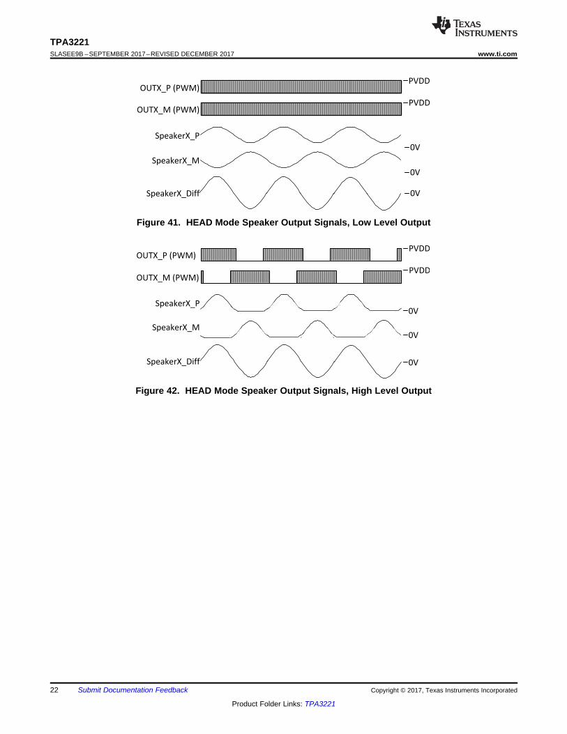
Figure 41. HEAD Mode Speaker Output Signals, Low Level Output
Figure 42. HEAD Mode Speaker Output Signals, High Level Output

23
TPA3221www.ti.com SLASEE9B –SEPTEMBER 2017–REVISED DECEMBER 2017
Product Folder Links: TPA3221
Submit Documentation FeedbackCopyright © 2017, Texas Instruments Incorporated
9.3.4 OscillatorThe oscillator frequency can be trimmed by external control of the FREQ_ADJ pin.
To reduce interference problems while using radio receiver tuned within the AM band, the switching frequencycan be changed from nominal to higher values. These values should be chosen such that the nominal and thehigher value switching frequencies together results in the fewest cases of interference throughout the AM band.The oscillator frequency can be selected by the value of the FREQ_ADJ resistor connected to GND in mastermode according to the description in the Recommended Operating Conditions table.
For slave mode operation, turn off the oscillator by pulling the FREQ_ADJ pin to AVDD. This configures theOSC_I/O pins as inputs to be slaved from an external differential clock. In a master/slave system inter channeldelay is automatically setup between the switching of the audio channels, which can be illustrated by no idlechannels switching at the same time. This will not influence the audio output, but only the switch timing tominimize noise coupling between audio channels through the power supply to optimize audio performance and toget better operating conditions for the power supply. The inter channel delay will be setup for a slave devicedepending on the polarity of the OSC_I/O connection such that a slave mode 1 is selected by connecting themaster device OSC_I/O to the slave 1 device OSC_I/O with same polarity (+ to + and - to -), and slave mode 2 isselected with the inverse polarity (+ to - and - to +).
9.3.5 Input ImpedanceThe TPA3221 input stage is a fully differential input stage and the input impedance changes with the gain settingfrom 7.7 kΩ at 34 dB gain to 47 kΩ at 18 dB gain. Table 1 lists the values from min to max gain. The tolerance ofthe input resistor value is ±20 % so the minimum value will be higher than 6.2 kΩ. The inputs need to be AC-coupled to minimize the output DC-offset and ensure correct ramping of the output voltages during power-ONand power-OFF. The input ac-coupling capacitor together with the input impedance forms a high-pass filter withthe following cut-off frequency:
If a flat bass response is required down to 20 Hz the recommended cut-off frequency is a tenth of that, 2 Hz.Table 3 lists the recommended ac-couplings capacitors for each gain step. If a -3 dB is accepted at 20 Hz 10times lower capacitors can used – for example, a 1 μF can be used.
Table 3. Recommended Input AC-Coupling Capacitors
Gain Input Impedance Input AC-CouplingCapacitance Input High Pass Filter
18 dB 48 kΩ 4.7 µF 0.7 Hz24 dB 24 kΩ 10 µF 0.7 Hz30 dB 12 kΩ 10 µF 1.3 Hz34 dB 7.7 kΩ 10 µF 2.1 Hz
The input capacitors used should be a type with low leakage, like quality electrolytic, tantalum, film or ceramic. Ifa polarized type is used the positive connection should face such that the capacitor has a positive DC bias.
9.3.6 Error ReportingThe FAULT, and OTW_CLIP, pins are active-low, open-drain outputs. The FAULT function is for protection-modesignaling to a system-control device. Any fault resulting in device shutdown is signaled by the FAULT pin goinglow. Also, OTW_CLIP goes low when the device junction temperature exceeds 125°C (see Table 4).
Table 4. Error ReportingFAULT OTW_CLIP DESCRIPTION
0 0 Overtemperature (OTE), overload (OLP), undervoltage (UVP), or overvoltage (OVP).Junction temperature higher than 125°C (overtemperature warning)
0 1 Overload (OLP), undervoltage (UVP), or overvoltage (OVP). Junction temperaturelower than 125°C
1 0 Junction temperature higher than 125°C (overtemperature warning)1 1 Junction temperature lower than 125°C and no OLP or UVP faults (normal operation)

TPA322xOUT2_P
OUT2_M
OUT1_M
OUT1_P
IN2_M
IN2_P
IN1_P
IN1_M
IN1_P
IN1_M
TPA322xOUT2_P
OUT2_M
OUT1_M
OUT1_P
IN2_M
IN2_P
IN1_P
IN1_M
IN1_P
IN1_M
TPA322xOUT2_P
OUT2_M
OUT1_M
OUT1_P
IN2_M
IN1_P
IN2_P
IN1_P
IN1_MIN1_M
IN2_P
IN2_M
TPA322xOUT2_P
OUT2_M
OUT1_M
OUT1_P
IN2_M
IN2_P
IN1_P
IN1_M
IN1_P
IN1_M
AVDD
24
TPA3221SLASEE9B –SEPTEMBER 2017–REVISED DECEMBER 2017 www.ti.com
Product Folder Links: TPA3221
Submit Documentation Feedback Copyright © 2017, Texas Instruments Incorporated
Note that asserting RESET low forces the FAULT signal high, independent of faults being present. TIrecommends monitoring the OTW_CLIP signal using the system microcontroller and responding to anovertemperature warning signal by turning down the volume to prevent further heating of the device resulting indevice shutdown (OTE).
To reduce external component count, an internal pullup resistor to 3.3 V is provided on both FAULT andOTW_CLIP outputs.
9.4 Device Functional ModesTPA3221 can be configured in either a stereo BTL (Bridge Tied Load) mode, mono BTL mode (only one outputBTL channel active), or in a mono PBTL (Parallel Bridge Tied Load) mode. In PBTL mode the two output BTLchannels are parallelled with double output current available. The parallelling of the two BTL outputs can bemade either before the output LC filter, or after the output LC filter. For PBTL mode the audio performance will ingeneral be higher when parallelling before the output LC filter, but parallelling after the LC output filter may bepreferred in some systems.
See Table 1 for mode configuration setup.
Figure 43. Stereo BTL Figure 44. Mono BTL
Figure 45. Mono PBTL, Pre LC Filter Figure 46. Mono PBTL, Post LC Filter
9.4.1 Powering UpThe TPA3221 does not require a power-up sequence because of the integrated undervoltage protection (UVP),but it is recommended to hold RESET low until PVDD supply voltage is stable to avoid audio artifacts. Theoutputs of the H-bridges remain in a high-impedance state until the gate-drive supply (GVDD) and AVDDvoltages are above their UVP voltage thresholds (see the Electrical Characteristics table of this data sheet). Thisallows an internal circuit to charge the external bootstrap capacitors by enabling a weak pull-down of the half-bridge output as well as initiating a controlled ramp up sequence of the output voltage.

PVDD
RESET
GVDD
FAULT
AVDD
VIN_X
OUT_X
VOUT_X
tPrecharge
C 20 ms
tStartup ramp
VDD
V_CMUTE
25
TPA3221www.ti.com SLASEE9B –SEPTEMBER 2017–REVISED DECEMBER 2017
Product Folder Links: TPA3221
Submit Documentation FeedbackCopyright © 2017, Texas Instruments Incorporated
Figure 47. Startup Timing
When RESET is released to turn on TPA3221, FAULT signal will turn low and AVDD voltage regulator will beenabled. FAULT will stay low until AVDD reaches the undervoltage protection (UVP) voltage threshold (see theElectrical Characteristics table of this data sheet). After a pre-charge time to stabilize the DC voltage across theinput AC coupling capacitors, the ramp up sequence starts and completes once the CMUTE node is charged toits final value.
9.4.1.1 Startup Ramp TimeDuring the startup ramp the CMUTE capacitor is charged by an internal current generator. With use of therecommended 33 nF CMUTE capacitor value, the startup ramp time is approximately 20 ms. Higher CMUTEcapacitor value will increase the ramp time, and a lower value will decrease the ramp time. The recommendedCMUTE capacitor value is selected for minimum audible artifacts during startup and shutdown ramp.
9.4.2 Powering DownThe TPA3221 does not require a power-down sequence. The device remains fully operational as long as theVDD, AVDD and PVDD voltages are above their undervoltage protection (UVP) voltage thresholds (see theElectrical Characteristics table of this data sheet). Although not specifically required, it is a good practice to holdRESET low during power down, thus preventing audible artifacts including pops or clicks by initiating a controlledramp down sequence of the output voltage. The ramp down sequence will complete once the CMUTE node isdischarged.

26
TPA3221SLASEE9B –SEPTEMBER 2017–REVISED DECEMBER 2017 www.ti.com
Product Folder Links: TPA3221
Submit Documentation Feedback Copyright © 2017, Texas Instruments Incorporated
9.4.2.1 Power Down Ramp TimeDuring the power down ramp the CMUTE capacitor is discharged by internal circuitry. With use of therecommended 33 nF CMUTE capacitor value, the power-down ramp time is approximately 20 ms.
9.4.3 Device ResetAsserting RESET low initiates the device ramp down. The output FETs go into a Hi-Z state after the ramp downis complete. Output pull downs are active in both BTL mode and PBTL mode with RESET low.
In BTL modes, to accommodate bootstrap charging prior to switching start, asserting the RESET input lowenables weak pull-down of the half-bridge outputs.
Asserting RESET low removes any fault information to be signaled on the FAULT output, that is, FAULT isforced high. A rising-edge transition on RESET allows the device to resume operation after a fault. To ensurethermal reliability, the rising edge of RESET must occur no sooner than 4 ms after the falling edge of FAULT.
The TPA3221 will enter a low power state once the ramp down sequence is complete.
9.4.4 Device Soft MuteAsserting CMUTE low initiates the device soft mute function. The soft mute function initiates a ramp downsequence of the outputs, and the output FETs go into a Hi-Z state after the ramp down is complete. All internalcircuits are powered while in soft mute state. External control of the soft mute function must provide highimpedance output when not engaged (open drain output) to allow the CMUTE node to charge/discharge duringdevice ramp up and ramp down when de-asserting and asserting RESET.
9.4.5 Device Protection SystemThe TPA3221 contains advanced protection circuitry carefully designed to facilitate system integration and easeof use, as well as to safeguard the device from permanent failure due to a wide range of fault conditions such asshort circuits, overload, overtemperature, overvoltage and undervoltage. The TPA3221 responds to a fault byimmediately setting the power stage in a high-impedance (Hi-Z) state and asserting the FAULT pin low. Insituations other than overload and overtemperature error (OTE), the device automatically recovers when the faultcondition has been removed, that is, the supply voltage has increased. The device will handle errors, as shownin Table 5.
Table 5. Device ProtectionBTL MODE PBTL MODE
LOCAL ERROR IN TURNS OFF LOCAL ERROR IN TURNS OFFA
A+BA
A+B+C+DB BC
C+DC
D D
Bootstrap UVP does not shutdown according to the table, it shuts down the respective halfbridge (non-latching,does not assert FAULT).
9.4.5.1 Overload and Short Circuit Current ProtectionTPA3221 has fast reacting current sensors on all high-side and low-side FETs. To prevent output current fromincreasing beyond the overcurrent threshold, TPA3221 uses current limiting of the output current for eachswitching cycle (Cycle By Cycle Current Control, CB3C) in case of excess output current. CB3C preventspremature shutdown due to high output current transients caused by high level music transients and a drop ofreal speaker’s load impedance, and allows the output current to be limited to a maximum programmed level. Ifthe maximum output current persists, i.e. the power stage being overloaded with too low load impedance, thedevice will shut down the affected output channel and the affected output is put in a high-impedance (Hi- Z) stateuntil a RESET cycle is initiated. CB3C works individually for each full-bridge output. If an over current event istriggered, CB3C performs a state flip of the full-bridged output that is cleared upon beginning of next PWMframe.

HS PWM
PWM_X
LS PWM
OC EVENT RESETS CB3C LATCH
OUTPUT CURRENT
OC THRESHOLD
OCH
HS GATE-DRIVE
LS GATE-DRIVE
RISING EDGE PWM SETS CB3C LATCH
27
TPA3221www.ti.com SLASEE9B –SEPTEMBER 2017–REVISED DECEMBER 2017
Product Folder Links: TPA3221
Submit Documentation FeedbackCopyright © 2017, Texas Instruments Incorporated
Figure 48. CB3C Timing Example
9.4.5.2 Signal Clipping and Pulse InjectorA built in activity detector monitors the PWM activity of the OUT_X pins. TPA3221 is designed to driveunclipped output signals all the way to PVDD and GND rails. In case of audio signal clipping when applyingexcessive input signal voltage, or in case of CB3C current protection being active, the amplifier feedbackloop of the audio channel will respond to this condition with a saturated state, and the output PWM signalswill stop unless special circuitry is implemented to handle this situation. To prevent the output PWM signalsfrom stopping in a clipping or CB3C situation, narrow pulses are injected to the gate drive to maintain outputactivity. The injected narrow pulses are injected at every 4th PWM frame, and thus the effective switchingfrequency during this state is reduced to 1/4 of the normal switching frequency.Signal clipping is signalled on the OTW_CLIP pin and is self clearing when signal level reduces and thedevice reverts to normal operation. The OTW_CLIP pulses starts at the onset to output clipping, typically at aTHD level around 0.01%, resulting in narrow OTW_CLIP pulses starting with a pulse width of ~500ns.
Figure 49. Signal Clipping PWM and Speaker Output Signals

28
TPA3221SLASEE9B –SEPTEMBER 2017–REVISED DECEMBER 2017 www.ti.com
Product Folder Links: TPA3221
Submit Documentation Feedback Copyright © 2017, Texas Instruments Incorporated
9.4.5.3 DC Speaker ProtectionThe output DC protection scheme protects a speaker from excess DC current in case one terminal of thespeaker is connected to the amplifier while the other is accidentally shorted to the chassis ground. Such a shortcircuit results in a DC voltage of PVDD/2 across the speaker, which potentially can result in destructive currentlevels. The output DC protection detects any unbalance of the output and input current of a BTL or PBTL outputconfiguration (current into/out of one half-bridge equals current out of/into the other half-bridge), and in the eventof the unbalance exceeding a programmed threshold, the overload counter increments until its maximum valueand the affected output channel is shut down. DC Speaker Protection is enabled in both BTL and PBTL modeoperation.
9.4.5.4 Pin-to-Pin Short Circuit Protection (PPSC)The PPSC detection system protects the device from permanent damage in the case that a power output pin(OUT_X) is shorted to GND_X or PVDD_X. For comparison, the OC protection system detects an overcurrentafter the demodulation filter where PPSC detects shorts directly at the pin before the filter. PPSC detection isperformed at startup after RESET is pulled high. When PPSC detection is activated by a short on the output, allhalf-bridges are kept in a Hi-Z state until the short is removed; the device then continues the startup sequenceand starts switching. The detection is controlled globally by a two step sequence. The first step ensures thatthere are no shorts from OUT_X to GND_X, the second step tests that there are no shorts from OUT_X toPVDD_X. The total duration of this process is roughly proportional to the capacitance of the output LC filter. Thetypical duration is < 15 ms/μF. While the PPSC detection is in progress, FAULT is kept low. If no shorts arepresent the PPSC detection passes, and FAULT is released. A device reset will start a new PPSC detection.PPSC detection is enabled in both BTL and PBTL output configurations. To make sure not to trip the PPSCdetection system it is recommended not to insert a resistive load to GND_X or PVDD_X.
9.4.5.5 Overtemperature Protection OTW and OTETPA3221 has a two-level temperature-protection system that asserts an active-low warning signal (OTW_CLIP)when the device junction temperature exceeds 125°C (typical) and, if the device junction temperature exceeds155°C (typical), the device is put into thermal shutdown, resulting in all half-bridge outputs being set in the high-impedance (Hi-Z) state and FAULT being asserted low. OTE is latched in this case. To clear the OTE latch,RESET must be asserted. Thereafter, the device resumes normal operation.
9.4.5.6 Undervoltage Protection (UVP), Overvoltage Protection (OVP) and Power-on Reset (POR)The UVP, OVP and POR circuits of the TPA3221 fully protect the device in any power-up/down, and brownoutsituation, and also in overvoltage situation with PVDD not exceeding the values stated in Absolute MaximumRatings. While powering up, the POR circuit ensures that all circuits are fully operational when the AVDD supplyvoltage reaches the value stated in the Electrical Characteristics table. Although AVDD is independentlymonitored, a supply voltage drop below the UVP threshold on AVDD pin results in all half-bridge outputsimmediately being set in the high-impedance (Hi-Z) state and FAULT being asserted low. The deviceautomatically resumes operation when all supply voltages have increased above their UVP threshold. In case ofan OVP event, all half-bridge outputs are immediately set in the high-impedance (Hi-Z) state and FAULT isasserted low until PVDD is below the OVP threshold.

29
TPA3221www.ti.com SLASEE9B –SEPTEMBER 2017–REVISED DECEMBER 2017
Product Folder Links: TPA3221
Submit Documentation FeedbackCopyright © 2017, Texas Instruments Incorporated
(1) Stuck at Fault occurs when input OSC_IO input signal frequency drops below minimum frequency given in the Electrical Characteristicstable of this data sheet.
9.4.5.7 Fault HandlingIf a fault situation occurs while in operation, the device acts accordingly to the fault being a global or a channelfault. A global fault is a chip-wide fault situation and causes all PWM activity of the device to be shut down, andwill assert FAULT low. A global fault is a latching fault and clearing FAULT and restarting operation requiresresetting the device by toggling RESET. De-asserting RESET should never be allowed with excessive systemtemperature, so it is advised to monitor RESET with a system microcontroller and only release RESET (RESEThigh) if the OTW_CLIP signal is cleared (high). A channel fault results in shutdown of the PWM activity of theaffected channel(s). Note that asserting RESET low forces the FAULT signal high, independent of faults beingpresent.
Table 6. Error Reporting
Fault/Event Fault/EventDescription Global or Channel Reporting Method Latched/Self
ClearingAction needed to
Clear Output FETs
PVDD_X UVP
Voltage Fault Global FAULT pin Self Clearing Increase affectedsupply voltage HI-ZPVDD_X OVP
AVDD UVP
POR (AVDD UVP) Power On Reset Global FAULT pin Self Clearing Allow AVDD to rise HI-Z
OTW Thermal Warning Global OTW pin Self Clearing Cool below OTWthreshold Normal operation
OTE Thermal Shutdown Global FAULT pin Latched Toggle RESET HI-Z
OLP (CB3C>1.7 ms) OC Shutdown Channel FAULT pin Latched Toggle RESET HI-Z
CB3C OC Limiting Channel None Self Clearing Reduce signal levelor remove short
Flip state, cycle bycycle at fs/3
Stuck at Fault (1) No OSC_IO activityin Slave Mode Global None Self Clearing Resume OSC_IO
activity HI-Z

PVDD
GNDTPA322x
PVDD
GND
BST1_P
PVDD
GND
OUT1_M
BST1_M
GND
OUT2_P
PVDD
OUT1_P
PVDD
GND
BST2_P
BST2_M
OUT2_M
GND
GND
OUT2_M
OUT1_P
PVDD
PVDD
44
43
42
41
31
27
28
29
30
32
33
34
35
36
40
39
38
37
25
26
23
24
13
14
15
16
17
18
1
2
3
4
5
6
7
8
9
10
11
12
19
20
21
22
1µF
1µF
1µF
1µF 470uF
470uF
10µH
10µH
1µF
1µF
1nF
10nF
3R3
10nF1nF
3R3
33nF
33nF
10µH
10µH
1µF
1µF
1nF
10nF
3R3
10nF1nF
3R3
33nF
33nF
Copyright © 2017, Texas Instruments Incorporated
GND
GAIN/SLV
FAULT
OTW_CLIP
AVDD
GND
CMUTE
IN2_M
OSCP
OSCM
GND
GND
IN2_P
GND
VDD
GVDD
GND
HEAD
FREQ_ADJ
IN1_P
IN1_M
RESET
100nF470uF
5.6k
/FAULT
/OTW_CLIP
1µF 1µF
+5V
CMUTE
IN1_P
IN1_M
/RESET
50k
1µF
1µF
3R3+5V
33nF
CMUTE
IN2_P
IN2_M
1µF
1µF
1k
30
TPA3221SLASEE9B –SEPTEMBER 2017–REVISED DECEMBER 2017 www.ti.com
Product Folder Links: TPA3221
Submit Documentation Feedback Copyright © 2017, Texas Instruments Incorporated
10 Application and Implementation
NOTEInformation in the following applications sections is not part of the TI componentspecification, and TI does not warrant its accuracy or completeness. TI’s customers areresponsible for determining suitability of components for their purposes. Customers shouldvalidate and test their design implementation to confirm system functionality.
10.1 Application InformationTPA3221 can be configured either in stereo BTL, mono BTL or mono PBTL mode depending on output powerconditions and system design.
10.2 Typical Applications
10.2.1 Stereo BTL Application
Figure 50. Typical Differential (2N) AD-Mode BTL Application

31
TPA3221www.ti.com SLASEE9B –SEPTEMBER 2017–REVISED DECEMBER 2017
Product Folder Links: TPA3221
Submit Documentation FeedbackCopyright © 2017, Texas Instruments Incorporated
Typical Applications (continued)10.2.1.1 Design RequirementsFor this design example, use the parameters in Table 7.
Table 7. Design Requirements, BTL ApplicationDESIGN PARAMETER EXAMPLE
ExternalLow Power Supply 5 VHigh Power Supply 7 - 30 V
Analog Inputs
IN1_M = ±2.8V (peak, max)IN1_P = ±2.8V (peak, max)IN2_M = ±2.8V (peak, max)IN2_P = ±2.8V (peak, max)
Output Filters Inductor-Capacitor Low Pass FIlter (10 µH + 1 µF)Speaker Impedance 3 - 8 Ω
10.2.1.2 Detailed Design ProceduresA rising-edge transition on RESET input allows the device to execute the startup sequence and starts switching.
A toggling OTW_CLIP signal is indicating that the output is approaching clipping. The signal can be used eitherto decrease audio volume or to control an intelligent power supply nominally operating at a low rail adjusting to ahigher supply rail.
The device inverts the audio signal from input to output.
The AVDD pin is not recommended to be used as a voltage source for external circuitry when internal LDO isenabled (VDD ≥ 7 V).
10.2.1.2.1 Decoupling Capacitor Recommendations
In order to design an amplifier that has robust performance, passes regulatory requirements, and exhibits goodaudio performance, good quality decoupling capacitors should be used. In practice, X7R should be used in thisapplication.
The voltage of the decoupling capacitors should be selected in accordance with good design practices.Temperature, ripple current, and voltage overshoot must be considered. This fact is particularly true in theselection of the 1μF that is placed on the power supply to each full-bridge. It must withstand the voltageovershoot of the PWM switching, the heat generated by the amplifier during high power output, and the ripplecurrent created by high power output. A minimum voltage rating of 50 V is required for use with a 30 V powersupply.
10.2.1.2.2 PVDD Capacitor Recommendation
The large capacitors used in conjunction with each full-bridge, are referred to as the PVDD Capacitors. Thesecapacitors should be selected for proper voltage margin and adequate capacitance to support the powerrequirements. In practice, with a well designed system power supply, 470 μF, 50 V supports most applications.The PVDD capacitors should be low ESR type because they are used in a circuit associated with high-speedswitching.
10.2.1.2.3 BST capacitors
To ensure large enough bootstrap energy storage for the high side gate drive to work correctly with all audiosource signals, 33 nF / 50V X7R BST capacitors are recommended.
10.2.1.2.4 PCB Material Recommendation
FR-4 Glass Epoxy material with 2 oz. (70 μm) copper is recommended for use with the TPA3221. The use of thismaterial can provide for higher power output, improved thermal performance, and better EMI margin (due tolower PCB trace inductance.

PVDD
GND
TPA322x
PVDD
GND
BST1_P
PVDD
GND
OUT1_M
BST1_M
GND
OUT2_P
PVDD
OUT1_P
PVDD
GND
BST2_P
BST2_M
OUT2_M
GND
GND
OUT2_M
OUT1_P
PVDD
PVDD
44
43
42
41
31
27
28
29
30
32
33
34
35
36
40
39
38
37
25
26
23
24
1µF
1µF
1µF
1µF 470uF
470uF 10µH
33nF
33nF
10µH
33nF
33nF
470nF
470nF
1nF
10nF
3R3
10nF1nF
3R3
470nF
470nF
Copyright © 2017, Texas Instruments Incorporated
13
14
15
16
17
18
1
2
3
4
5
6
7
8
9
10
11
12
19
20
21
22
GND
GAIN/SLV
FAULT
OTW_CLIP
AVDD
GND
CMUTE
IN2_M
OSCP
OSCM
GND
GND
IN2_P
GND
VDD
GVDD
GND
HEAD
FREQ_ADJ
IN1_P
IN1_M
RESET
100nF470uF
5.6k
/FAULT
/OTW_CLIP
+5V
IN1_P
IN1_M
/RESET
50k
1µF
1µF
1µF 1µF
CMUTE
3R3+5V
33nF
CMUTE
1k
32
TPA3221SLASEE9B –SEPTEMBER 2017–REVISED DECEMBER 2017 www.ti.com
Product Folder Links: TPA3221
Submit Documentation Feedback Copyright © 2017, Texas Instruments Incorporated
10.2.2 Typical Application, Differential (2N), AD-Mode PBTL (Outputs Paralleled before LC filter)TPA3221 can be configured in mono PBTL mode by paralleling the outputs before the LC filter or after the LCfilter (see Typical Application, Differential (2N), AD-Mode PBTL (Outputs Paralleled after LC filter)). Paralleledoutputs before the LC filter is recommended for better performance and limiting the number of output LC filterinductors,
Figure 51. Typical Differential (2N) AD-Mode PBTL Application
10.2.2.1 Design RequirementsRefer to Stereo BTL Application for the Design Requirements.
Table 8. Design Requirements, PBTL ApplicationDESIGN PARAMETER EXAMPLE
Low Power Supply 5 VHigh Power Supply 7 - 30 V
Analog Inputs
IN1_M = ±2.8 V (peak, max)IN1_P = ±2.8 V (peak, max)
IN2_M = GroundedIN2_P = Grounded
Output Filters Inductor-Capacitor Low Pass FIlter (10 µH + 1 µF)Speaker Impedance 2 - 4 Ω
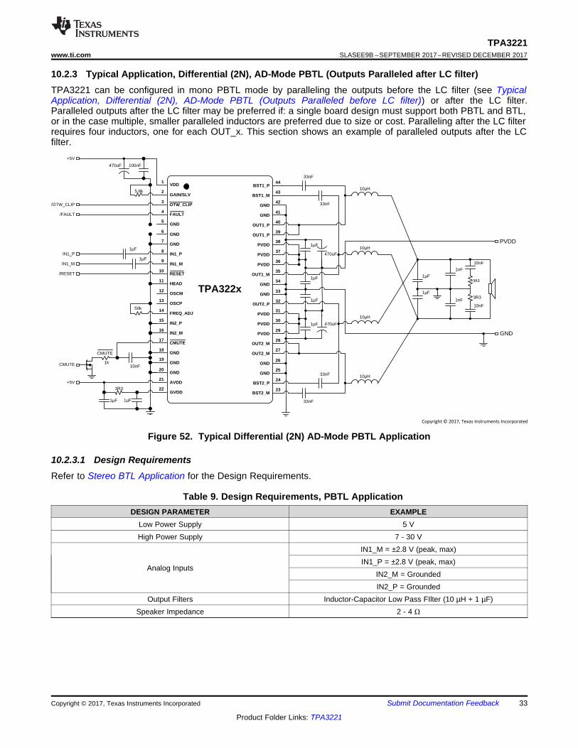
PVDD
GND
TPA322x
PVDD
GND
BST1_P
PVDD
GND
OUT1_M
BST1_M
GND
OUT2_P
PVDD
OUT1_P
PVDD
GND
BST2_P
BST2_M
OUT2_M
GND
GND
OUT2_M
OUT1_P
PVDD
PVDD
44
43
42
41
31
27
28
29
30
32
33
34
35
36
40
39
38
37
25
26
23
24
1µF
1µF
1µF
1µF 470uF
470uF
10µH
10µH
33nF
33nF
10µH
10µH33nF
33nF
1µF
1µF
1nF
10nF
3R3
10nF1nF
3R3
Copyright © 2017, Texas Instruments Incorporated
13
14
15
16
17
18
1
2
3
4
5
6
7
8
9
10
11
12
19
20
21
22
GND
GAIN/SLV
FAULT
OTW_CLIP
AVDD
GND
CMUTE
IN2_M
OSCP
OSCM
GND
GND
IN2_P
GND
VDD
GVDD
GND
HEAD
FREQ_ADJ
IN1_P
IN1_M
RESET
100nF470uF
5.6k
/FAULT
/OTW_CLIP
+5V
IN1_P
IN1_M
/RESET
50k
1µF
1µF
1µF 1µF
CMUTE
3R3+5V
33nF
CMUTE
1k
33
TPA3221www.ti.com SLASEE9B –SEPTEMBER 2017–REVISED DECEMBER 2017
Product Folder Links: TPA3221
Submit Documentation FeedbackCopyright © 2017, Texas Instruments Incorporated
10.2.3 Typical Application, Differential (2N), AD-Mode PBTL (Outputs Paralleled after LC filter)TPA3221 can be configured in mono PBTL mode by paralleling the outputs before the LC filter (see TypicalApplication, Differential (2N), AD-Mode PBTL (Outputs Paralleled before LC filter)) or after the LC filter.Paralleled outputs after the LC filter may be preferred if: a single board design must support both PBTL and BTL,or in the case multiple, smaller paralleled inductors are preferred due to size or cost. Paralleling after the LC filterrequires four inductors, one for each OUT_x. This section shows an example of paralleled outputs after the LCfilter.
Figure 52. Typical Differential (2N) AD-Mode PBTL Application
10.2.3.1 Design RequirementsRefer to Stereo BTL Application for the Design Requirements.
Table 9. Design Requirements, PBTL ApplicationDESIGN PARAMETER EXAMPLE
Low Power Supply 5 VHigh Power Supply 7 - 30 V
Analog Inputs
IN1_M = ±2.8 V (peak, max)IN1_P = ±2.8 V (peak, max)
IN2_M = GroundedIN2_P = Grounded
Output Filters Inductor-Capacitor Low Pass FIlter (10 µH + 1 µF)Speaker Impedance 2 - 4 Ω

34
TPA3221SLASEE9B –SEPTEMBER 2017–REVISED DECEMBER 2017 www.ti.com
Product Folder Links: TPA3221
Submit Documentation Feedback Copyright © 2017, Texas Instruments Incorporated
11 Power Supply Recommendations
11.1 Power SuppliesThe TPA3221 device requires a single external power supply for proper operation. A high-voltage supply, PVDD,is required to power the output stage of the speaker amplifier and its associated circuitry. PVDD can be used tosupply an internal LDO to supply 5 V to AVDD and GVDD (connect VDD to PVDD).
Additionally, in LDO bypass mode an external power supply should be connected to VDD, AVDD and GVDD topower the gate-drive and other internal digital and analog circuit blocks in the device.
The allowable voltage range for both the PVDD and VDD/AVDD/GVDD supplies are listed in the RecommendedOperating Conditions table. Ensure both the PVDD and the VDD/AVDD/GVDD supplies can deliver more currentthan listed in the Electrical Characteristics table.
11.1.1 VDD SupplyVDD can be connected to PVDD in systems using only a single power supply. VDD is connected to an internalLDO that is then used to supply AVDD and GVDD for digital and analog circuits as well as to supply the gatedrive.
To reduce device power consumption, the internal LDO can be bypassed by connecting VDD, AVDD and GVDDto an external 5 V power supply.
Proper connection, routing, and decoupling techniques are highlighted in the TPA3221 device EVM User's Guide(as well as the Application Information section and Layout Examples section) and must be followed as closely aspossible for proper operation and performance. Deviation from the guidance offered in the TPA3221 device EVMUser's Guide, which followed the same techniques as those shown in the Application Information section, mayresult in reduced performance, errant functionality, or even damage to the TPA3221 device. To simplify thepower supply requirements for the system, the TPA3221 device includes a integrated low-dropout (LDO) linearregulator to create a 5V rail for AVDD and GVDD supplies. The linear regulator is internally connected to theVDD supply and its output is present on the AVDD pin, providing a connection point for an external bypasscapacitors. It is important to note that the linear regulator integrated in the device has only been designed tosupport the current requirements of the internal circuitry, and should not be used to power any additional externalcircuitry. Additional loading on these pins could cause the voltage to sag and increase noise injection, whichnegatively affects the performance and operation of the device.
11.1.2 AVDD and GVDD SuppliesAVDD and GVDD can be supplied either through the internal LDO or from external 5 V power supply to powerinternal analog and digital circuits and the gate-drives for the output H-bridges. Proper connection, routing, anddecoupling techniques are highlighted in the TPA3221 device EVM User's Guide (as well as the ApplicationInformation section and Layout Examples section) and must be followed as closely as possible for properoperation and performance. Deviation from the guidance offered in the TPA3221 device EVM User's Guide,which followed the same techniques as those shown in the Application Information section, may result in reducedperformance, errant functionality, or even damage to the TPA3221 device.
11.1.3 PVDD SupplyThe output stage of the speaker amplifier drives the load using the PVDD supply. This is the power supply whichprovides the drive current to the load during playback. Proper connection, routing, and decoupling techniques arehighlighted in the TPA3221 device EVM User's Guide (as well as the Application Information section and LayoutExamples section) and must be followed as closely as possible for proper operation and performance. Due thehigh-voltage switching of the output stage, it is particularly important to properly decouple the output powerstages in the manner described in the TPA3221 device EVM User's Guide. The lack of proper decoupling, likethat shown in the EVM User's Guide, can results in voltage spikes which can damage the device, or cause pooraudio performance and device shutdown faults.

35
TPA3221www.ti.com SLASEE9B –SEPTEMBER 2017–REVISED DECEMBER 2017
Product Folder Links: TPA3221
Submit Documentation FeedbackCopyright © 2017, Texas Instruments Incorporated
Power Supplies (continued)11.1.4 BST SupplyTPA3221 has built-in bootstrap supply for each half bridge gate drive to supply the high side MOSFETs, onlyrequiring a single capacitor per half bridge. The capacitors are connected to each half bridge output, and arecharged by the GVDD supply via an internal diode while the PWM outputs are in low state. The high side gatedrive is supplied by the voltage across the BST capacitor while the output PWM is high. It is recommended toplace the BST capacitors close to the TPA3221 device, and to keep PCB routing traces at minimum length.
12 Layout
12.1 Layout Guidelines• Use an unbroken ground plane to have good low impedance and inductance return path to the power supply
for power and audio signals.• Maintain a contiguous ground plane from the ground pins to the PCB area surrounding the device for as
many of the ground pins as possible, since the ground pins are the best conductors of heat in the package.• PCB layout, audio performance and EMI are linked closely together.• Routing the audio input should be kept short and together with the accompanied audio source ground.• The small bypass capacitors on the PVDD lines should be placed as close the PVDD pins as possible.• A local ground area underneath the device is important to keep solid to minimize ground bounce.• Orient the passive component so that the narrow end of the passive component is facing the TPA3221
device, unless the area between two pads of a passive component is large enough to allow copper to flow inbetween the two pads.
• Avoid placing other heat producing components or structures near the TPA3221 device.• Avoid cutting off the flow of heat from the TPA3221 device to the surrounding ground areas with traces or via
strings, especially on output side of device.
Netlist for this printed circuit board is generated from the schematic in Figure 53.
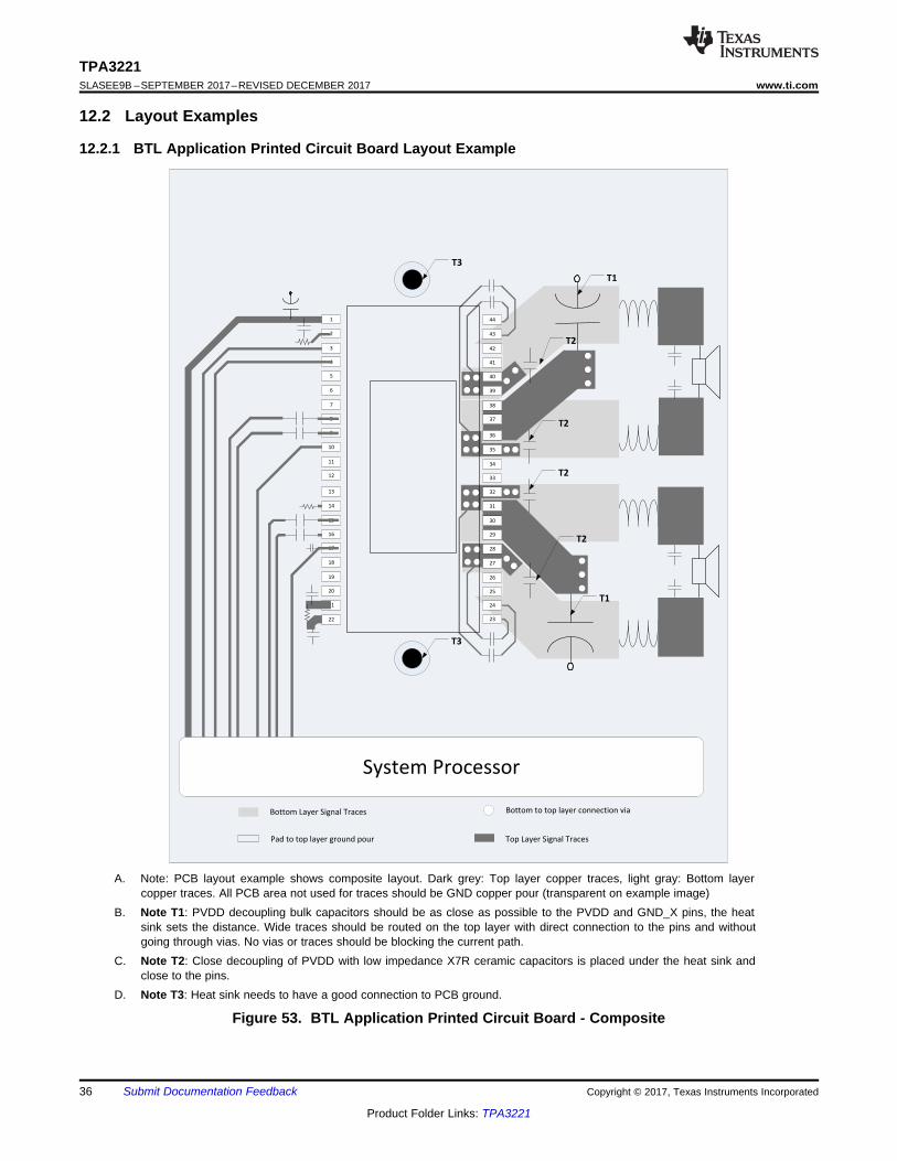
21
22
20
17
18
15
16
13
14
11
12
9
10
7
1
26
25
28
27
30
32
31
34
33
36
35
38
37
40
39
42
41
Bottom Layer Signal Traces
Top Layer Signal Traces
Bottom to top layer connection via
Pad to top layer ground pour
3
4
2
29
24
23
8
43
44
System Processor
19
6
5
T1
T2
T2
T1
T3
T3
T2
T2
36
TPA3221SLASEE9B –SEPTEMBER 2017–REVISED DECEMBER 2017 www.ti.com
Product Folder Links: TPA3221
Submit Documentation Feedback Copyright © 2017, Texas Instruments Incorporated
12.2 Layout Examples
12.2.1 BTL Application Printed Circuit Board Layout Example
A. Note: PCB layout example shows composite layout. Dark grey: Top layer copper traces, light gray: Bottom layercopper traces. All PCB area not used for traces should be GND copper pour (transparent on example image)
B. Note T1: PVDD decoupling bulk capacitors should be as close as possible to the PVDD and GND_X pins, the heatsink sets the distance. Wide traces should be routed on the top layer with direct connection to the pins and withoutgoing through vias. No vias or traces should be blocking the current path.
C. Note T2: Close decoupling of PVDD with low impedance X7R ceramic capacitors is placed under the heat sink andclose to the pins.
D. Note T3: Heat sink needs to have a good connection to PCB ground.
Figure 53. BTL Application Printed Circuit Board - Composite

21
22
20
17
18
15
16
13
14
11
12
9
10
7
1
26
25
28
27
30
32
31
34
33
36
35
38
37
40
39
42
41
Bottom Layer Signal Traces
Top Layer Signal Traces
Bottom to top layer connection via
Pad to top layer ground pour
3
4
2
29
24
23
8
43
44
System Processor
19
6
5
T3
T3
T2
T1
T1
T2
T2
T2
37
TPA3221www.ti.com SLASEE9B –SEPTEMBER 2017–REVISED DECEMBER 2017
Product Folder Links: TPA3221
Submit Documentation FeedbackCopyright © 2017, Texas Instruments Incorporated
Layout Examples (continued)12.2.2 PBTL (Outputs Paralleled before LC filter) Application Printed Circuit Board Layout Example
A. Note: PCB layout example shows composite layout. Dark grey: Top layer copper traces, light gray: Bottom layercopper traces. All PCB area not used for traces should be GND copper pour (transparent on example image)
B. Note T1: PVDD decoupling bulk capacitors should be as close as possible to the PVDD and GND_X pins, the heatsink sets the distance. Wide traces should be routed on the top layer with direct connection to the pins and withoutgoing through vias. No vias or traces should be blocking the current path.
C. Note T2: Close decoupling of PVDD with low impedance X7R ceramic capacitors is placed under the heat sink andclose to the pins.
D. Note T3: Heat sink needs to have a good connection to PCB ground.
Figure 54. PBTL (Outputs Paralleled before LC filter) Application Printed Circuit Board - Composite

21
22
20
17
18
15
16
13
14
11
12
9
10
7
1
26
25
28
27
30
32
31
34
33
36
35
38
37
40
39
42
41
Bottom Layer Signal Traces
Top Layer Signal Traces
Bottom to top layer connection via
Pad to top layer ground pour
3
4
2
29
24
23
8
43
44
System Processor
19
6
5
T1
T2
T2
T1
T3
T3
T2
T2
38
TPA3221SLASEE9B –SEPTEMBER 2017–REVISED DECEMBER 2017 www.ti.com
Product Folder Links: TPA3221
Submit Documentation Feedback Copyright © 2017, Texas Instruments Incorporated
Layout Examples (continued)12.2.3 PBTL (Outputs Paralleled after LC filter) Application Printed Circuit Board Layout Example
A. Note: PCB layout example shows composite layout. Dark grey: Top layer copper traces, light gray: Bottom layercopper traces. All PCB area not used for traces should be GND copper pour (transparent on example image)
B. Note T1: PVDD decoupling bulk capacitors should be as close as possible to the PVDD and GND_X pins, the heatsink sets the distance. Wide traces should be routed on the top layer with direct connection to the pins and withoutgoing through vias. No vias or traces should be blocking the current path.
C. Note T2: Close decoupling of PVDD with low impedance X7R ceramic capacitors is placed under the heat sink andclose to the pins.
D. ote T3: Heat sink needs to have a good connection to PCB ground.
Figure 55. PBTL (Outputs Paralleled after LC filter) Application Printed Circuit Board - Composite
39
TPA3221www.ti.com SLASEE9B –SEPTEMBER 2017–REVISED DECEMBER 2017
Product Folder Links: TPA3221
Submit Documentation FeedbackCopyright © 2017, Texas Instruments Incorporated
13 Device and Documentation Support
13.1 Documentation SupportTPA3221 Evaluation Module User's Guide
13.2 Receiving Notification of Documentation UpdatesTo receive notification of documentation updates, navigate to the device product folder on ti.com. In the upperright corner, click on Alert me to register and receive a weekly digest of any product information that haschanged. For change details, review the revision history included in any revised document
13.3 Community ResourcesThe following links connect to TI community resources. Linked contents are provided "AS IS" by the respectivecontributors. They do not constitute TI specifications and do not necessarily reflect TI's views; see TI's Terms ofUse.
TI E2E™ Online Community TI's Engineer-to-Engineer (E2E) Community. Created to foster collaborationamong engineers. At e2e.ti.com, you can ask questions, share knowledge, explore ideas and helpsolve problems with fellow engineers.
Design Support TI's Design Support Quickly find helpful E2E forums along with design support tools andcontact information for technical support.
13.4 TrademarksE2E is a trademark of Texas Instruments.
13.5 Electrostatic Discharge CautionThese devices have limited built-in ESD protection. The leads should be shorted together or the device placed in conductive foamduring storage or handling to prevent electrostatic damage to the MOS gates.
13.6 GlossarySLYZ022 — TI Glossary.
This glossary lists and explains terms, acronyms, and definitions.
14 Mechanical, Packaging, and Orderable InformationThe following pages include mechanical, packaging, and orderable information. This information is the mostcurrent data available for the designated devices. This data is subject to change without notice and revision ofthis document. For browser-based versions of this data sheet, refer to the left-hand navigation.
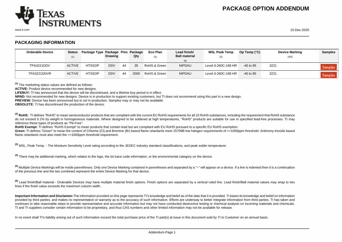
PACKAGE OPTION ADDENDUM
www.ti.com 10-Dec-2020
Addendum-Page 1
PACKAGING INFORMATION
Orderable Device Status(1)
Package Type PackageDrawing
Pins PackageQty
Eco Plan(2)
Lead finish/Ball material
(6)
MSL Peak Temp(3)
Op Temp (°C) Device Marking(4/5)
Samples
TPA3221DDV ACTIVE HTSSOP DDV 44 35 RoHS & Green NIPDAU Level-3-260C-168 HR -40 to 85 3221
TPA3221DDVR ACTIVE HTSSOP DDV 44 2000 RoHS & Green NIPDAU Level-3-260C-168 HR -40 to 85 3221
(1) The marketing status values are defined as follows:ACTIVE: Product device recommended for new designs.LIFEBUY: TI has announced that the device will be discontinued, and a lifetime-buy period is in effect.NRND: Not recommended for new designs. Device is in production to support existing customers, but TI does not recommend using this part in a new design.PREVIEW: Device has been announced but is not in production. Samples may or may not be available.OBSOLETE: TI has discontinued the production of the device.
(2) RoHS: TI defines "RoHS" to mean semiconductor products that are compliant with the current EU RoHS requirements for all 10 RoHS substances, including the requirement that RoHS substancedo not exceed 0.1% by weight in homogeneous materials. Where designed to be soldered at high temperatures, "RoHS" products are suitable for use in specified lead-free processes. TI mayreference these types of products as "Pb-Free".RoHS Exempt: TI defines "RoHS Exempt" to mean products that contain lead but are compliant with EU RoHS pursuant to a specific EU RoHS exemption.Green: TI defines "Green" to mean the content of Chlorine (Cl) and Bromine (Br) based flame retardants meet JS709B low halogen requirements of <=1000ppm threshold. Antimony trioxide basedflame retardants must also meet the <=1000ppm threshold requirement.
(3) MSL, Peak Temp. - The Moisture Sensitivity Level rating according to the JEDEC industry standard classifications, and peak solder temperature.
(4) There may be additional marking, which relates to the logo, the lot trace code information, or the environmental category on the device.
(5) Multiple Device Markings will be inside parentheses. Only one Device Marking contained in parentheses and separated by a "~" will appear on a device. If a line is indented then it is a continuationof the previous line and the two combined represent the entire Device Marking for that device.
(6) Lead finish/Ball material - Orderable Devices may have multiple material finish options. Finish options are separated by a vertical ruled line. Lead finish/Ball material values may wrap to twolines if the finish value exceeds the maximum column width.
Important Information and Disclaimer:The information provided on this page represents TI's knowledge and belief as of the date that it is provided. TI bases its knowledge and belief on informationprovided by third parties, and makes no representation or warranty as to the accuracy of such information. Efforts are underway to better integrate information from third parties. TI has taken andcontinues to take reasonable steps to provide representative and accurate information but may not have conducted destructive testing or chemical analysis on incoming materials and chemicals.TI and TI suppliers consider certain information to be proprietary, and thus CAS numbers and other limited information may not be available for release.
In no event shall TI's liability arising out of such information exceed the total purchase price of the TI part(s) at issue in this document sold by TI to Customer on an annual basis.
PACKAGE OPTION ADDENDUM
www.ti.com 10-Dec-2020
Addendum-Page 2

TAPE AND REEL INFORMATION
*All dimensions are nominal
Device PackageType
PackageDrawing
Pins SPQ ReelDiameter
(mm)
ReelWidth
W1 (mm)
A0(mm)
B0(mm)
K0(mm)
P1(mm)
W(mm)
Pin1Quadrant
TPA3221DDVR HTSSOP DDV 44 2000 330.0 24.4 8.6 15.6 1.8 12.0 24.0 Q1
PACKAGE MATERIALS INFORMATION
www.ti.com 14-Feb-2019
Pack Materials-Page 1

*All dimensions are nominal
Device Package Type Package Drawing Pins SPQ Length (mm) Width (mm) Height (mm)
TPA3221DDVR HTSSOP DDV 44 2000 350.0 350.0 43.0
PACKAGE MATERIALS INFORMATION
www.ti.com 14-Feb-2019
Pack Materials-Page 2


www.ti.com
PACKAGE OUTLINE
C
TYP8.37.9
42X 0.635
44X 0.270.17
2X13.335
(0.15) TYP
0 - 80.150.05
1.21.0
7.306.72
4.433.85
0.25GAGE PLANE
0.750.50
A
NOTE 3
14.113.9
B 6.26.0
(0.15) TYPNOTE 6
2X (0.6)NOTE 6
2X (0.3)NOTE 6
PowerPAD TSSOP - 1.2 mm max heightDDV0044DPLASTIC SMALL OUTLINE
4218830/A 08/2016
NOTES: 1. All linear dimensions are in millimeters. Any dimensions in parenthesis are for reference only. Dimensioning and tolerancing per ASME Y14.5M. 2. This drawing is subject to change without notice. 3. This dimension does not include mold flash, protrusions, or gate burrs. Mold flash, protrusions, or gate burrs shall not exceed 0.15 mm per side.4. Reference JEDEC registration MO-153.5. The exposed thermal pad is designed to be attached to an external heatsink.6. Features may differ or may not be present.
PowerPAD is a trademark of Texas Instruments.
TM
144
0.08 C A B
2322
PIN 1 IDAREA
EXPOSEDTHERMALPAD
SEATING PLANE
0.1 C
SEE DETAIL A
DETAIL ATYPICAL
SCALE 1.250

www.ti.com
EXAMPLE BOARD LAYOUT
(7.5)
0.05 MAXAROUND
0.05 MINAROUND
44X (1.45)
44X (0.4)
42X (0.635)
(R0.05) TYP
PowerPAD TSSOP - 1.2 mm max heightDDV0044DPLASTIC SMALL OUTLINE
4218830/A 08/2016
SYMM
SYMM
SEE DETAILS
LAND PATTERN EXAMPLESCALE:6X
1
22 23
44
NOTES: (continued) 7. Publication IPC-7351 may have alternate designs. 8. Solder mask tolerances between and around signal pads can vary based on board fabrication site.
TM
METALSOLDER MASKOPENING
NON SOLDER MASKDEFINED
SOLDER MASK DETAILSNOT TO SCALE
OPENINGSOLDER MASK METAL UNDER
SOLDER MASK
SOLDER MASKDEFINED

www.ti.com
EXAMPLE STENCIL DESIGN
44X (1.45)
44X (0.4)
42X (0.635)
(7.5)
PowerPAD TSSOP - 1.2 mm max heightDDV0044DPLASTIC SMALL OUTLINE
4218830/A 08/2016
NOTES: (continued) 9. Laser cutting apertures with trapezoidal walls and rounded corners may offer better paste release. IPC-7525 may have alternate design recommendations. 10. Board assembly site may have different recommendations for stencil design.
TM
SOLDER PASTE EXAMPLEBASED ON 0.125 MM THICK STENCIL
SCALE :6X
SYMM
SYMM
1
22 23
44

IMPORTANT NOTICE AND DISCLAIMER
TI PROVIDES TECHNICAL AND RELIABILITY DATA (INCLUDING DATASHEETS), DESIGN RESOURCES (INCLUDING REFERENCE DESIGNS), APPLICATION OR OTHER DESIGN ADVICE, WEB TOOLS, SAFETY INFORMATION, AND OTHER RESOURCES “AS IS” AND WITH ALL FAULTS, AND DISCLAIMS ALL WARRANTIES, EXPRESS AND IMPLIED, INCLUDING WITHOUT LIMITATION ANY IMPLIED WARRANTIES OF MERCHANTABILITY, FITNESS FOR A PARTICULAR PURPOSE OR NON-INFRINGEMENT OF THIRD PARTY INTELLECTUAL PROPERTY RIGHTS.These resources are intended for skilled developers designing with TI products. You are solely responsible for (1) selecting the appropriate TI products for your application, (2) designing, validating and testing your application, and (3) ensuring your application meets applicable standards, and any other safety, security, or other requirements. These resources are subject to change without notice. TI grants you permission to use these resources only for development of an application that uses the TI products described in the resource. Other reproduction and display of these resources is prohibited. No license is granted to any other TI intellectual property right or to any third party intellectual property right. TI disclaims responsibility for, and you will fully indemnify TI and its representatives against, any claims, damages, costs, losses, and liabilities arising out of your use of these resources.TI’s products are provided subject to TI’s Terms of Sale (www.ti.com/legal/termsofsale.html) or other applicable terms available either on ti.com or provided in conjunction with such TI products. TI’s provision of these resources does not expand or otherwise alter TI’s applicable warranties or warranty disclaimers for TI products.
Mailing Address: Texas Instruments, Post Office Box 655303, Dallas, Texas 75265Copyright © 2020, Texas Instruments Incorporated