Embed Size (px)
Citation preview

Please be aware that an important notice concerning availability, standard warranty, and use in critical applications ofTexas Instruments semiconductor products and disclaimers thereto appears at the end of this data sheet.
TPA02022-W STEREO AUDIO POWER AMPLIFIER
SLOS205B – FEBRUARY 1998 – REVISED DECEMBER 2000
1POST OFFICE BOX 655303 • DALLAS, TEXAS 75265
Integrated Depop Circuitry
High Power with PC Power Supply– 2 W/Ch at 5 V into a 3-Ω Load– 800 mW/Ch at 3 V
Fully Specified for Use With 3-Ω Loads
Ultra-Low Distortion– 0.05% THD+N at 2 W and 3-Ω Load
Bridge-Tied Load (BTL) or Single-Ended(SE) Modes
Stereo Input MUX
Surface-Mount Power Package24-Pin TSSOP PowerPAD
Shutdown Control . . . IDD = 5 µA
CBCS
RightMUX
RLINEIN
RHPIN
LeftMUX
LHPIN
LLINEIN
Bias, Mute,Shutdown,and SE/BTLMUX Control
+–
+–
RBYPASS
MUTE IN
MUTE OUT
SHUTDOWN
LBYPASS
ROUT+
ROUT–
RVDD
LVDD
LOUT+
LOUT–
SE/BTL
HP/LINE
CIR
RIR
RFRCFR
SystemControl
CIL
RIL
NC
NC
4
5
6
8
9
11
19
20
21
RFLCFL
100 kΩ
100 kΩ
VDD
VDD
COUTR
COUTL
10
3
16
7
14
18
15
22
1 kΩ
1 kΩ
1
2
3
4
5
6
78
9
10
11
12
24
23
22
21
20
19
1817
16
15
14
13
GND/HSTJ
LOUT+LLINEIN
LHPINLBYPASS
LVDDSHUTDOWN
MUTE OUTLOUT–
MUTE INGND/HS
GND/HSNCROUT+RLINEINRHPINRBYPASSRVDDNCHP/LINEROUT–SE/BTLGND/HS
PWP PACKAGE(TOP VIEW)
Copyright 2000, Texas Instruments IncorporatedPRODUCTION DATA information is current as of publication date.Products conform to specifications per the terms of Texas Instrumentsstandard warranty. Production processing does not necessarily includetesting of all parameters.
PowerPAD is a trademark of Texas Instruments Incorporated.

TPA02022-W STEREO AUDIO POWER AMPLIFIER
SLOS205B – FEBRUARY 1998 – REVISED DECEMBER 2000
2 POST OFFICE BOX 655303 • DALLAS, TEXAS 75265
description
The TPA0202 is a stereo audio power amplifier in a 24-pin TSSOP thermal package capable of deliveringgreater than 2 W of continuous RMS power per channel into 3-Ω loads. The TPA0202 simplifies design and freesup board space for other features. Full power distortion levels of less than 0.1% THD+N from a 5-V supply aretypical. Low-voltage applications are also well served by the TPA0202 providing 800-mW per channel into 3-Ωloads with a 3.3-V supply voltage.
The TPA0202 has integrated depop circuitry that virtually eliminates transients that cause noise in the speakersduring power up and when using the mute and shutdown modes.
Amplifier gain is externally configured by means of two resistors per input channel and does not require externalcompensation for settings of 2 to 20 in BTL mode (1 to 10 in SE mode). An internal input MUX allows two setsof stereo inputs to the amplifier. In notebook applications, where internal speakers are driven as BTL and theline (often headphone drive) outputs are required to be SE, the TPA0202 automatically switches into SE modewhen the SE/BTL input is activated. Using the TPA0202 to drive line outputs up to 700 mW/channel into external3-Ω loads is ideal for small non-powered external speakers in portable multimedia systems. The TPA0202 alsofeatures a shutdown function for power sensitive applications, holding the supply current at 5 µA.
The PowerPAD package† (PWP) delivers a level of thermal performance that was previously achievable onlyin TO-220-type packages. Thermal impedances of approximately 35°C/W are readily realized in multilayer PCBapplications. This allows the TPA0202 to operate at full power into 3-Ω loads at ambient temperature of up to85°C with 300 CFM of forced-air cooling. Into 8-Ω loads, the operating ambient temperature increases to 100°C.
AVAILABLE OPTIONS
PACKAGE
TA TSSOP‡
(PWP)
–40°C to 85°C TPA0202PWP
‡ The PWP packages are available taped and reeled. To order a tapedand reeled part, add the suffix R (e.g., TPA0202PWPR).
† See Texas Instruments document, PowerPAD Thermally Enhanced Package Application Report (Literature Number SLMA002) for moreinformation on the PowerPAD package.

TPA02022-W STEREO AUDIO POWER AMPLIFIER
SLOS205B – FEBRUARY 1998 – REVISED DECEMBER 2000
3POST OFFICE BOX 655303 • DALLAS, TEXAS 75265
Terminal Functions
TERMINALI/O DESCRIPTION
NAME NO.I/O DESCRIPTION
GND/HS 1, 12,13, 24
Ground connection for circuitry, directly connected to thermal pad
HP/LINE 16 I Input MUX control input, hold high to select LHP IN or RHP IN (5, 20), hold low to select LLINE IN orRLINE IN (4, 21)
LBYPASS 6 Tap to voltage divider for left channel internal mid-supply bias
LHP IN 5 I Left channel headphone input, selected when HP/LINE terminal (16) is held high
LLINE IN 4 I Left channel line input, selected when HP/LINE terminal (16) is held low
LOUT+ 3 O Left channel + output in BTL mode, + output in SE mode
LOUT– 10 O Left channel – output in BTL mode, high-impedance state in SE mode
LVDD 7 I Supply voltage input for left channel and for primary bias circuits
MUTE IN 11 I Mute all amplifiers, hold low for normal operation, hold high to mute
MUTE OUT 9 O Follows MUTE IN terminal (11), provides buffered output
NC 17, 23 No internal connection
RBYPASS 19 Tap to voltage divider for right channel internal mid–supply bias
RHPIN 20 I Right channel headphone input, selected when HP/LINE terminal (16) is held high
RLINEIN 21 I Right channel line input, selected when HP/LINE terminal (16) is held low
ROUT+ 22 O Right channel + output in BTL mode, + output in SE mode
ROUT– 15 O Right channel – output in BTL mode, high impedance state in SE mode
RVDD 18 I Supply voltage input for right channel
SE/BTL 14 I Hold low for BTL mode, hold high for SE mode
SHUTDOWN 8 I Places entire IC in shutdown mode when held high, IDD = 5 µA
TJ 2 O Sources a current proportional to the junction temperature. This terminal should be left unconnectedduring normal operation. For more information, see the junction temperature measurement section ofthis document.

TPA02022-W STEREO AUDIO POWER AMPLIFIER
SLOS205B – FEBRUARY 1998 – REVISED DECEMBER 2000
4 POST OFFICE BOX 655303 • DALLAS, TEXAS 75265
absolute maximum ratings over operating free-air temperature range (unless otherwise noted)†
Supply voltage, VDD 6 V. . . . . . . . . . . . . . . . . . . . . . . . . . . . . . . . . . . . . . . . . . . . . . . . . . . . . . . . . . . . . . . . . . . . . . . . Input voltage, VI –0.3 V to VDD +0.3 V. . . . . . . . . . . . . . . . . . . . . . . . . . . . . . . . . . . . . . . . . . . . . . . . . . . . . . . . . . . . Continuous total power dissipation internally limited (see Dissipation Rating Table). . . . . . . . . . . . . . . . . . . . . Operating free-air temperature range, TA –40°C to 85°C. . . . . . . . . . . . . . . . . . . . . . . . . . . . . . . . . . . . . . . . . . . . Operating junction temperature range, TJ –40°C to 150°C. . . . . . . . . . . . . . . . . . . . . . . . . . . . . . . . . . . . . . . . . . . Storage temperature range, Tstg –65°C to 150°C. . . . . . . . . . . . . . . . . . . . . . . . . . . . . . . . . . . . . . . . . . . . . . . . . . . Lead temperature 1,6 mm (1/16 inch) from case for 10 seconds 260°C. . . . . . . . . . . . . . . . . . . . . . . . . . . . . . .
† Stresses beyond those listed under “absolute maximum ratings” may cause permanent damage to the device. These are stress ratings only, andfunctional operation of the device at these or any other conditions beyond those indicated under “recommended operating conditions” is notimplied. Exposure to absolute-maximum-rated conditions for extended periods may affect device reliability.
DISSIPATION RATING TABLE
PACKAGE TA ≤ 25°C DERATING FACTOR TA = 70°C TA = 85°C
PWP‡ 2.7 W 21.8 mW/°C 1.7 W 1.4 W
‡ Please see the Texas Instruments document, PowerPAD Thermally Enhanced Package Application Report(literature number SLMA002), for more information on the PowerPAD package. The thermal data wasmeasured on a PCB layout based on the information in the section entitled Texas Instruments RecommendedBoard for PowerPAD on page 33 of the before mentioned document.
recommended operating conditions
MIN NOM MAX UNIT
Supply Voltage, VDD 3 5 5.5 V
VDD = 5 V, 250 mW/ch average power,
4-Ω stereo BTL drive, with proper PCB design
–40 85
Operating free-air temperature, TAVDD = 5 V,2 W/ch average power,
3-Ω stereo BTL drive,with proper PCB designand 300 CFM forced-aircooling
–40 85
°C
Common mode input voltage VICMVDD = 5 V 1.25 4.5
VCommon mode input voltage, VICMVDD = 3.3 V 1.25 2.7
V
dc electrical characteristics, TA = 25°CPARAMETER TEST CONDITIONS TYP† MAX UNIT
Stereo BTL 19 30 mA
VDD = 5 VStereo SE 9 18 mA
VDD = 5 VMono BTL 9 18 mA
IDD Supply currentMono SE 3 10 mA
IDD Supply currentStereo BTL 13 20 mA
VDD = 3 3 VStereo SE 5 10 mA
VDD = 3.3 VMono BTL 5 10 mA
Mono SE 3 6 mA
VOO Output offset voltage (measured differentially) VDD = 5 V, Gain = 2, See Note 1 5 25 mV
IDD(MUTE) Supply current in mute mode VDD = 5 V 1.5 mA
IDD(SD) IDD in shutdown VDD = 5 V 5 20 µA
NOTE 1: At 3 V < VDD < 5 V the dc output voltage is approximately VDD/2.

TPA02022-W STEREO AUDIO POWER AMPLIFIER
SLOS205B – FEBRUARY 1998 – REVISED DECEMBER 2000
5POST OFFICE BOX 655303 • DALLAS, TEXAS 75265
ac operating characteristics, VDD = 5 V, TA = 25°C, RL = 3 Ω (unless otherwise noted)
PARAMETER TEST CONDITIONS TYP MAX UNIT
POOutput power (each channel) see THD = 0.2%, BTL, See Figure 3 2
WPO( )
Note 2 THD = 1%, BTL, See Figure 3 2.2W
THD+N Total harmonic distortion plus noisePo = 2W, f = 20 – 20 kHz, See Figure 5 200 m%
THD+N Total harmonic distortion plus noiseVI = 1 V, RL = 10 kΩ, AV = 1 V/V 100 m%
BOM Maximum output power bandwidth AV = 10 V/V THD < 1 %, See Figure 5 >20 kHz
Phase margin RL = 4 Ω, Open Loop, See Figure 43 85°
Supply ripple rejection ratiof = 1 kHz, See Figure 37 80
dBSupply ripple rejection ratiof = 20 – 20 kHz, See Figure 37 60
dB
Mute attenuation 85 dB
Channel-to-channel output separation f = 1 kHz, See Figure 39 85 dB
Line/HP input separation 100 dB
BTL attenuation in SE mode 100 dB
ZI Input impedance 2 MΩ
Signal-to-noise ratio Po = 500 mW, BTL 95 dB
Vn Output noise voltage See Figure 35 21 µV(rms)
NOTE 2: Output power is measured at the output terminals of the IC at 1 kHz.
ac operating characteristics, VDD = 3.3 V, TA = 25°C, RL = 3 ΩPARAMETER TEST CONDITIONS TYP MAX UNIT
POOutput power (each channel) see THD = 0.2%, BTL, See Figure 10 800
mWPO( )
Note 2 THD = 1%, BTL, See Figure 10 900mW
THD+N Total harmonic distortion plus noisePo = 800 mW, f = 20 – 20 kHz, See Figure 11 350 m%
THD+N Total harmonic distortion plus noiseVI = 1 V, RL = 10 kΩ, AV = 1 V/V 200 m%
BOM Maximum output power bandwidth AV = 10 V/V THD < 1 %, See Figure 11 >20 kHz
Phase margin RL = 4 Ω, Open Loop, See Figure 44 85°
Supply ripple rejection ratiof = 1 kHz, See Figure 37 70
dBSupply ripple rejection ratiof = 20 – 20 kHz, See Figure 37 55
dB
Mute attenuation 85 dB
Channel-to-channel output separation f = 1 kHz, See Figure 40 85 dB
Line/HP input separation 100 dB
BTL attenuation in SE mode 100 dB
ZI Input impedance 2 MΩ
Signal-to-noise ratio Po = 500 mW, BTL 95 dB
Vn Output noise voltage See Figure 37 21 µV(rms)
NOTE 2: Output power is measured at the output terminals of the IC at 1 kHz.

TPA02022-W STEREO AUDIO POWER AMPLIFIER
SLOS205B – FEBRUARY 1998 – REVISED DECEMBER 2000
6 POST OFFICE BOX 655303 • DALLAS, TEXAS 75265
PARAMETER MEASUREMENT INFORMATION
MUXRICI
RF
4.7 µFCB SE/BTL
HP/LINE
RL = 3 Ω or 8 Ω
Figure 1. BTL Test Circuit
MUXRICI
RF
CB
CO
SE/BTL
HP/LINE
RL = 3 Ω, 8 Ω, or 32 Ω
4.7 µF
VDD
Figure 2. SE Test Circuit

TPA02022-W STEREO AUDIO POWER AMPLIFIER
SLOS205B – FEBRUARY 1998 – REVISED DECEMBER 2000
7POST OFFICE BOX 655303 • DALLAS, TEXAS 75265
TYPICAL CHARACTERISTICS
Table of GraphsFIGURE
THD + N Total harmonic distortion plus noise
vs Frequency4, 5, 7, 8, 11, 12, 14, 15, 17, 18, 20,
21, 23, 24, 26, 27, 29, 30 32, 33THD + N Total harmonic distortion plus noise
vs Output power3, 6, 9, 10, 13, 16, 19, 22, 25, 28, 31,
34
Vn Output noise voltage vs Frequency 35,36
Supply ripple rejection ratio vs Frequency 37,38
Crosstalk vs Frequency 39 – 42
Open loop response vs Frequency 43,44
Closed loop response vs Frequency 45, 48
IDD Supply current vs Supply voltage 49
PO Output powervs Supply voltagevs Load resistance
50, 5152, 53
PD Power dissipation vs Output power 54 – 57
Figure 3
0.1
0.010 0.25 0.5 0.75 1 1.25 1.5
1
10
1.75 2 2.25 2.5
PO – Output Power – W
VDD = 5 Vf = 1 kHzBTL
TH
D+N
–To
tal H
arm
on
ic D
isto
rtio
n +
No
ise
– %
TOTAL HARMONIC DISTORTION PLUS NOISEvs
OUTPUT POWER
RL = 8 Ω
RL = 3 Ω
Figure 4
0.01
10
20 100 1 k 10 k 20 k
TH
D+N
–To
tal H
arm
on
ic D
isto
rtio
n +
No
ise
– %
f – Frequency – Hz
TOTAL HARMONIC DISTORTION PLUS NOISEvs
FREQUENCY
1
0.1
VDD = 5 VPO = 1.5 WRL = 4 ΩBTL
AV = –2 V/V
AV = –20 V/V
AV = –10 V/V (RL = 3 Ω, PO = 2 W)
AV = –10 V/V
TPA02022-W STEREO AUDIO POWER AMPLIFIER
SLOS205B – FEBRUARY 1998 – REVISED DECEMBER 2000
8 POST OFFICE BOX 655303 • DALLAS, TEXAS 75265
TYPICAL CHARACTERISTICS
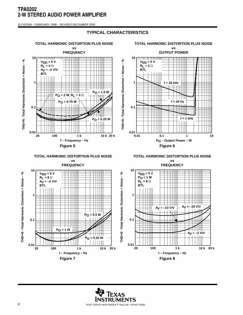
Figure 5
PO = 1.5 W
PO = 0.25 W
VDD = 5 VRL = 4 ΩAV = –2 V/VBTL
0.1
0.0120 100 1 k
1
10
10 k 20 k
TH
D+N
–To
tal H
arm
on
ic D
isto
rtio
n +
No
ise
– %
f – Frequency – Hz
TOTAL HARMONIC DISTORTION PLUS NOISEvs
FREQUENCY
PO = 0.75 W
PO = 2 W, RL = 3 Ω
Figure 6
f = 20 kHz
f = 1 kHz
f = 20 Hz
0.1
0.010.01 0.1
1
10
1 10
PO – Output Power – W
VDD = 5 VRL = 3 ΩBTL
TH
D+N
–To
tal H
arm
on
ic D
isto
rtio
n +
No
ise
– %
TOTAL HARMONIC DISTORTION PLUS NOISEvs
OUTPUT POWER
Figure 7
0.1
0.0120 100 1 k
1
10
10 k 20 k
TH
D+N
–To
tal H
arm
on
ic D
isto
rtio
n +
No
ise
– %
f – Frequency – Hz
TOTAL HARMONIC DISTORTION PLUS NOISEvs
FREQUENCY
PO = 1 W
VDD = 5 VRL = 8 ΩAV = –2 V/VBTL
PO = 0.25 W
PO = 0.5 W
Figure 8
0.1
0.0120 100 1 k
1
10
10 k 20 k
TH
D+N
–To
tal H
arm
on
ic D
isto
rtio
n +
No
ise
– %
f – Frequency – Hz
TOTAL HARMONIC DISTORTION PLUS NOISEvs
FREQUENCY
VDD = 5 VPO = 1 WRL = 8 ΩBTL
AV = –2 V/V
AV =– 20 V/VAV = –10 V/V

TPA02022-W STEREO AUDIO POWER AMPLIFIER
SLOS205B – FEBRUARY 1998 – REVISED DECEMBER 2000
9POST OFFICE BOX 655303 • DALLAS, TEXAS 75265
TYPICAL CHARACTERISTICS
Figure 9
0.1
0.010.01 0.1
1
10
1 10
f = 20 kHz
f = 1 kHz
f = 20 Hz
PO – Output Power – W
VDD = 5 VRL = 8 ΩAV = –2 V/VBTL
TH
D+N
–To
tal H
arm
on
ic D
isto
rtio
n +
No
ise
– %
TOTAL HARMONIC DISTORTION PLUS NOISEvs
OUTPUT POWER
Figure 10
0.1
0.010 0.1 0.2 0.3 0.4 0.5 0.6
1
10
0.7 0.8 0.9 1
PO – Output Power – W
VDD = 3.3 Vf = 1 kHzBTL
TH
D+N
–To
tal H
arm
on
ic D
isto
rtio
n +
No
ise
– %
TOTAL HARMONIC DISTORTION PLUS NOISEvs
OUTPUT POWER
RL = 3 ΩRL = 8 Ω
Figure 11
0.1
0.0120 100 1 k
1
10
10 k 20 k
TH
D+N
–To
tal H
arm
on
ic D
isto
rtio
n +
No
ise
– %
f – Frequency – Hz
TOTAL HARMONIC DISTORTION PLUS NOISEvs
FREQUENCY
VDD = 3.3 VPO = 0.75 WRL = 4 ΩBTL
AV = –10 V/V
AV = –20 V/V
AV = –2 V/V
AV = –10 V/V (RL = 3 Ω, PO = 800 mW)
Figure 12
PO = 0.35 W
PO = 0.1 W
PO = 0.75 W
0.1
0.0120 100 1 k
1
10
10 k 20 k
TH
D+N
–To
tal H
arm
on
ic D
isto
rtio
n +
No
ise
– %
f – Frequency – Hz
TOTAL HARMONIC DISTORTION PLUS NOISEvs
FREQUENCY
VDD = 3.3 VRL = 4 ΩAV = –2 V/VBTL
PO = 800 mW(RL = 3 Ω)
TPA02022-W STEREO AUDIO POWER AMPLIFIER
SLOS205B – FEBRUARY 1998 – REVISED DECEMBER 2000
10 POST OFFICE BOX 655303 • DALLAS, TEXAS 75265
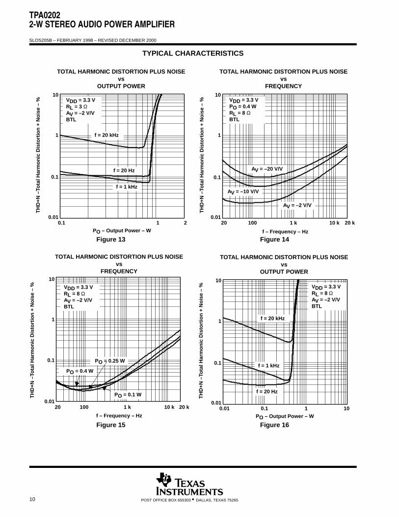
TYPICAL CHARACTERISTICS
Figure 13
0.1
0.010.1
1
10
1 2
f = 20 kHz
f = 1 kHz
f = 20 Hz
PO – Output Power – W
VDD = 3.3 VRL = 3 ΩAV = –2 V/VBTL
TH
D+N
–To
tal H
arm
on
ic D
isto
rtio
n +
No
ise
– %
TOTAL HARMONIC DISTORTION PLUS NOISEvs
OUTPUT POWER
Figure 14
0.1
0.0120 100 1 k
1
10
10 k 20 k
TH
D+N
–To
tal H
arm
on
ic D
isto
rtio
n +
No
ise
– %
f – Frequency – Hz
TOTAL HARMONIC DISTORTION PLUS NOISEvs
FREQUENCY
AV = –20 V/V
AV = –10 V/V
AV = –2 V/V
VDD = 3.3 VPO = 0.4 WRL = 8 ΩBTL
Figure 15
PO = 0.4 W
PO = 0.25 W
PO = 0.1 W
VDD = 3.3 VRL = 8 ΩAV = –2 V/VBTL
0.1
0.0120 100 1 k
1
10
10 k 20 k
TH
D+N
–To
tal H
arm
on
ic D
isto
rtio
n +
No
ise
– %
f – Frequency – Hz
TOTAL HARMONIC DISTORTION PLUS NOISEvs
FREQUENCY
Figure 16
0.1
0.010.01 0.1
1
10
1 10
f = 20 kHz
f = 1 kHz
f = 20 Hz
PO – Output Power – W
VDD = 3.3 VRL = 8 ΩAV = –2 V/VBTL
TH
D+N
–To
tal H
arm
on
ic D
isto
rtio
n +
No
ise
– %
TOTAL HARMONIC DISTORTION PLUS NOISEvs
OUTPUT POWER

TPA02022-W STEREO AUDIO POWER AMPLIFIER
SLOS205B – FEBRUARY 1998 – REVISED DECEMBER 2000
11POST OFFICE BOX 655303 • DALLAS, TEXAS 75265
TYPICAL CHARACTERISTICS
Figure 17
0.1
0.0120 100 1 k
1
10
10 k 20 k
AV = –10 V/V
AV = –5 V/V
AV = –1 V/V
TH
D+N
–To
tal H
arm
on
ic D
isto
rtio
n +
No
ise
– %
f – Frequency – Hz
TOTAL HARMONIC DISTORTION PLUS NOISEvs
FREQUENCY
VDD = 5 VPO = 0.5 WRL = 4 ΩSE
Figure 18
0.1
0.0120 100 1 k
1
10
10 k 20 k
PO = 0.25 W
PO = 0.1 W
PO = 0.5 W
TH
D+N
–To
tal H
arm
on
ic D
isto
rtio
n +
No
ise
– %
f – Frequency – Hz
TOTAL HARMONIC DISTORTION PLUS NOISEvs
FREQUENCY
VDD = 5 VRL = 4 ΩAV = –2 V/VSE
Figure 19
f = 20 kHz
f =100 Hz
f = 1 kHz
VDD = 5 VRL = 4 ΩAV = –2 V/VSE
0.1
0.010.001 0.01
1
10
0.1 1PO – Output Power – W
TH
D+N
–To
tal H
arm
on
ic D
isto
rtio
n +
No
ise
– %
TOTAL HARMONIC DISTORTION PLUS NOISEvs
OUTPUT POWER
Figure 20
0.1
0.0120 100 1 k
1
10
10 k 20 k
AV = –10 V/V
AV = –5 V/V
AV = –1 V/V
TH
D+N
–To
tal H
arm
on
ic D
isto
rtio
n +
No
ise
– %
f – Frequency – Hz
TOTAL HARMONIC DISTORTION PLUS NOISEvs
FREQUENCY
VDD = 5 VPO = 0.25 WRL = 8 ΩSE

TPA02022-W STEREO AUDIO POWER AMPLIFIER
SLOS205B – FEBRUARY 1998 – REVISED DECEMBER 2000
12 POST OFFICE BOX 655303 • DALLAS, TEXAS 75265
TYPICAL CHARACTERISTICS
Figure 21
0.1
0.0120 100 1 k
1
10
10 k 20 k
PO = 0.25 W
PO = 0.05 W
PO = 0.1 W
TH
D+N
–To
tal H
arm
on
ic D
isto
rtio
n +
No
ise
– %
f – Frequency – Hz
TOTAL HARMONIC DISTORTION PLUS NOISEvs
FREQUENCY
VDD = 5 VRL = 8 ΩSE
Figure 22
0.1
0.010.001 0.1
1
10
1
PO – Output Power – W
VDD = 5 VRL = 8 ΩAV = –2 V/VSE
TH
D+N
–To
tal H
arm
on
ic D
isto
rtio
n +
No
ise
– %
TOTAL HARMONIC DISTORTION PLUS NOISEvs
OUTPUT POWER
0.01
f = 20 kHz
f = 1 kHz
f = 100 Hz
Figure 23
0.1
0.0120 100 1 k
1
10
10 k 20 k
AV = –10 V/V
AV = –5 V/V
AV = –1 V/V
TH
D+N
–To
tal H
arm
on
ic D
isto
rtio
n +
No
ise
– %
f – Frequency – Hz
TOTAL HARMONIC DISTORTION PLUS NOISEvs
FREQUENCY
VDD = 5 VPO = 0.075 WRL = 32 ΩSE
Figure 24
0.1
0.0120 100 1 k
1
10
10 k 20 k
PO = 75 mW
PO = 25 mW
PO = 50 mW
TH
D+N
–To
tal H
arm
on
ic D
isto
rtio
n +
No
ise
– %
f – Frequency – Hz
TOTAL HARMONIC DISTORTION PLUS NOISEvs
FREQUENCY
VDD = 5 VRL = 32 ΩSE
TPA02022-W STEREO AUDIO POWER AMPLIFIER
SLOS205B – FEBRUARY 1998 – REVISED DECEMBER 2000
13POST OFFICE BOX 655303 • DALLAS, TEXAS 75265
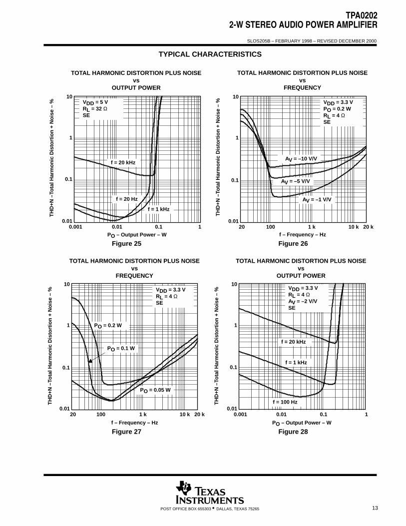
TYPICAL CHARACTERISTICS
Figure 25
0.1
0.010.001 0.01
1
10
0.1 1
f = 20 kHz
f = 1 kHz
f = 20 Hz
PO – Output Power – W
VDD = 5 VRL = 32 ΩSE
TH
D+N
–To
tal H
arm
on
ic D
isto
rtio
n +
No
ise
– %
TOTAL HARMONIC DISTORTION PLUS NOISEvs
OUTPUT POWER
Figure 26
0.1
0.0120 100 1 k
1
10
10 k 20 k
AV = –10 V/V
AV = –5 V/V
AV = –1 V/V
TH
D+N
–To
tal H
arm
on
ic D
isto
rtio
n +
No
ise
– %
f – Frequency – Hz
TOTAL HARMONIC DISTORTION PLUS NOISEvs
FREQUENCY
VDD = 3.3 VPO = 0.2 WRL = 4 ΩSE
Figure 27
0.1
0.0120 100 1 k
1
10
10 k 20 k
PO = 0.05 W
PO = 0.1 W
PO = 0.2 W
TH
D+N
–To
tal H
arm
on
ic D
isto
rtio
n +
No
ise
– %
f – Frequency – Hz
TOTAL HARMONIC DISTORTION PLUS NOISEvs
FREQUENCY
VDD = 3.3 VRL = 4 ΩSE
Figure 28
f = 100 Hz
f = 1 kHz
f = 20 kHz
VDD = 3.3 VRL = 4 ΩAV = –2 V/VSE
0.1
0.010.001 0.01
1
10
10.1
PO – Output Power – W
TH
D+N
–To
tal H
arm
on
ic D
isto
rtio
n +
No
ise
– %
TOTAL HARMONIC DISTORTION PLUS NOISEvs
OUTPUT POWER

TPA02022-W STEREO AUDIO POWER AMPLIFIER
SLOS205B – FEBRUARY 1998 – REVISED DECEMBER 2000
14 POST OFFICE BOX 655303 • DALLAS, TEXAS 75265
TYPICAL CHARACTERISTICS
Figure 29
AV = –10 V/V
AV = –5 V/VAV = –1 V/V
VDD = 3.3 VPO = 100 mWRL = 8 ΩSE
0.1
0.0120 100 1 k
1
10
10 k 20 k
TH
D+N
–To
tal H
arm
on
ic D
isto
rtio
n +
No
ise
– %
f – Frequency – Hz
TOTAL HARMONIC DISTORTION PLUS NOISEvs
FREQUENCY
Figure 30
0.1
0.0120 100 1 k
1
10
10 k 20 k
PO = 25 mW
PO = 50 mW
PO = 100 mW
TH
D+N
–To
tal H
arm
on
ic D
isto
rtio
n +
No
ise
– %
f – Frequency – Hz
TOTAL HARMONIC DISTORTION PLUS NOISEvs
FREQUENCY
VDD = 3.3 VRL = 8 ΩSE
Figure 31
VDD = 3.3 VRL = 8 ΩSE
0.1
0.010.001 0.1
1
10
1PO – Output Power – W
TH
D+N
–To
tal H
arm
on
ic D
isto
rtio
n +
No
ise
– %
TOTAL HARMONIC DISTORTION PLUS NOISEvs
OUTPUT POWER
f = 20 kHz
f = 1 kHz
f = 100 Hz
0.01
Figure 32
0.1
0.0120 100 1 k
1
10
10 k 20 k
AV = –10 V/V
AV = –5 V/V
AV = –1 V/V
TH
D+N
–To
tal H
arm
on
ic D
isto
rtio
n +
No
ise
– %
f – Frequency – Hz
TOTAL HARMONIC DISTORTION PLUS NOISEvs
FREQUENCY
VDD = 3.3 VPO = 30 mWRL = 32 ΩSE
TPA02022-W STEREO AUDIO POWER AMPLIFIER
SLOS205B – FEBRUARY 1998 – REVISED DECEMBER 2000
15POST OFFICE BOX 655303 • DALLAS, TEXAS 75265
TYPICAL CHARACTERISTICS
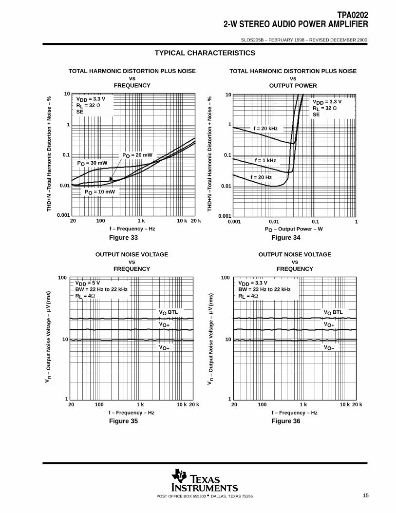
Figure 33
0.1
0.01
0.00120 100 1 k
1
10
10 k 20 k
PO = 10 mW
PO = 20 mW
PO = 30 mW
TH
D+N
–To
tal H
arm
on
ic D
isto
rtio
n +
No
ise
– %
f – Frequency – Hz
TOTAL HARMONIC DISTORTION PLUS NOISEvs
FREQUENCY
VDD = 3.3 VRL = 32 ΩSE
Figure 34
0.1
0.01
0.0010.001 0.01
1
10
0.1 1
f = 20 Hz
f = 1 kHz
f = 20 kHz
PO – Output Power – W
VDD = 3.3 VRL = 32 ΩSE
TH
D+N
–To
tal H
arm
on
ic D
isto
rtio
n +
No
ise
– %
TOTAL HARMONIC DISTORTION PLUS NOISEvs
OUTPUT POWER
Figure 35
10
120 100 1 k
f – Frequency – Hz
OUTPUT NOISE VOLTAGEvs
FREQUENCY100
10 k 20 k
VDD = 5 VBW = 22 Hz to 22 kHzRL = 4Ω
VO BTL
VO+
VO–
– O
utp
ut
No
ise
Vo
ltag
e –
Vn
Vµ
(rm
s)
Figure 36
10
120 100 1 k
f – Frequency – Hz
OUTPUT NOISE VOLTAGEvs
FREQUENCY100
10 k 20 k
VDD = 3.3 VBW = 22 Hz to 22 kHzRL = 4Ω
VO BTL
VO+
VO–
– O
utp
ut
No
ise
Vo
ltag
e –
Vn
Vµ
(rm
s)

TPA02022-W STEREO AUDIO POWER AMPLIFIER
SLOS205B – FEBRUARY 1998 – REVISED DECEMBER 2000
16 POST OFFICE BOX 655303 • DALLAS, TEXAS 75265
TYPICAL CHARACTERISTICS
Figure 37
–50
–60
–80
–10020 100 1 k
–30
–20
f – Frequency – Hz
SUPPLY RIPPLE REJECTION RATIOvs
FREQUENCY0
10 k 20 k
–10
–40
–70
–90VDD = 5 V
VDD = 3.3 V
RL = 4 ΩCB = 4.7 µFBTL
Su
pp
ly R
ipp
le R
ejec
tio
n R
atio
– d
B
Figure 38
–50
–60
–80
–10020 100 1 k
–30
–20
f – Frequency – Hz
SUPPLY RIPPLE REJECTION RATIOvs
FREQUENCY0
10 k 20 k
–10
–40
–70
–90
VDD = 5 V
VDD = 3.3 V
RL = 4 ΩCB = 4.7 µFSE
Su
pp
ly R
ipp
le R
ejec
tio
n R
atio
– d
B
Figure 39
Left to Right
Right to Left
–80
–90
–110
–120
–60
–50
–40
–70
–100
20 100 1 k
Cro
ssta
lk –
dB
f – Frequency – Hz
CROSSTALKvs
FREQUENCY
10 k 20 k
VDD = 5 VPO = 1.5 WRL = 4 ΩBTL
Figure 40
–80
–90
–110
–120
–60
–50
–40
–70
–100
20 100 1 k
Cro
ssta
lk –
dB
f – Frequency – Hz
CROSSTALKvs
FREQUENCY
10 k 20 k
VDD = 3.3 VPO = 0.75 WRL = 4 ΩBTL
Left to Right
Right to Left
TPA02022-W STEREO AUDIO POWER AMPLIFIER
SLOS205B – FEBRUARY 1998 – REVISED DECEMBER 2000
17POST OFFICE BOX 655303 • DALLAS, TEXAS 75265
TYPICAL CHARACTERISTICS
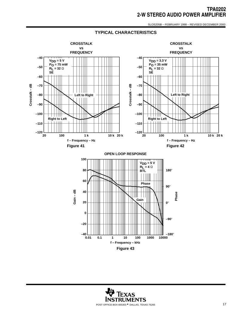
Figure 41
–80
–90
–110
–120
–60
–50
–40
–70
–100
20 100 1 k
Cro
ssta
lk –
dB
f – Frequency – Hz
CROSSTALKvs
FREQUENCY
10 k 20 k
VDD = 5 VPO = 75 mWRL = 32 ΩSE
Left to Right
Right to Left
Figure 42
–80
–90
–110
–120
–60
–50
–40
–70
–100
20 100 1 k
Cro
ssta
lk –
dB
f – Frequency – Hz
CROSSTALKvs
FREQUENCY
10 k 20 k
VDD = 3.3 VPO = 35 mWRL = 32 ΩSE
Left to Right
Right to Left
40
20
–20
–400.01
Gai
n –
dB
60
80
f – Frequency – kHz
OPEN LOOP RESPONSE100
0
0.1 1 10 100 1000 10000
180°
90°
0°
–90°
–180°
VDD = 5 VRL = 4 ΩBTL
Gain
Phase
Figure 43
Ph
ase
TPA02022-W STEREO AUDIO POWER AMPLIFIER
SLOS205B – FEBRUARY 1998 – REVISED DECEMBER 2000
18 POST OFFICE BOX 655303 • DALLAS, TEXAS 75265
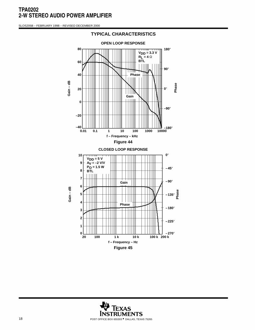
TYPICAL CHARACTERISTICS
20
0
–20
–40
40
60
80 180°
90°
0°
–90°
–180°0.01
Gai
n –
dB
f – Frequency – kHz
OPEN LOOP RESPONSE
0.1 1 10 100 1000 10000
VDD = 3.3 VRL = 4 ΩBTL
Gain
Figure 44
Phase
Ph
ase
5
3
2
020 100 1 k 10 k
Gai
n –
dB
7
9
f – Frequency – Hz
CLOSED LOOP RESPONSE
10
100 k 200 k
8
6
4
1
–45°
0°
–90°
–135°
–180°
–225°
–270°
Ph
ase
Phase
Gain
VDD = 5 VAV = –2 V/VPO = 1.5 WBTL
Figure 45

TPA02022-W STEREO AUDIO POWER AMPLIFIER
SLOS205B – FEBRUARY 1998 – REVISED DECEMBER 2000
19POST OFFICE BOX 655303 • DALLAS, TEXAS 75265
TYPICAL CHARACTERISTICS
5
3
2
020 100 1 k 10 k
Gai
n –
dB
7
9
f – Frequency – Hz
CLOSED LOOP RESPONSE
10
100 k 200 k
8
6
4
1
–45°
0°
–90°
–135°
–180°
–225°
–270°
Ph
ase
Phase
Gain
VDD = 3.3 VAV = –2 V/VPO = 0.75 WBTL
Figure 46
Figure 47
–5
–7
–8
–1020 100 1 k 10 k
Gai
n –
dB
–3
–1
f – Frequency – Hz
CLOSED LOOP RESPONSE
0
100 k 200 k
–2
–4
–6
–9
–45°
0°
–90°
–135°
–180°
–225°
–270°
Ph
ase
VDD = 5 VAV = –1 V/VPO = 0.5 WSE
Phase
Gain

TPA02022-W STEREO AUDIO POWER AMPLIFIER
SLOS205B – FEBRUARY 1998 – REVISED DECEMBER 2000
20 POST OFFICE BOX 655303 • DALLAS, TEXAS 75265
TYPICAL CHARACTERISTICS
–5
–7
–8
–1020 100 1 k 10 k
Gai
n –
dB
–3
–1
f – Frequency – Hz
CLOSED LOOP RESPONSE
0
100 k 200 k
–2
–4
–6
–9
–45°
0°
–90°
–135°
–180°
–225°
–270°
Ph
ase
VDD = 3.3VAV = –1 V/VPO = 0.25 WSE
Phase
Gain
Figure 48
Figure 49
Stereo BTL15
10
5
03
20
25
SUPPLY CURRENTvs
SUPPLY VOLTAGE30
4 65VDD – Supply Voltage – V
Stereo SE
– S
up
ply
Cu
rren
t –
mA
ÁÁÁÁI
DD
Figure 50
1.5
1
0.5
02.5 3 3.5 4 4.5 5
2
2.5
3
5.5 6
RL = 4Ω
RL = 8 Ω
– O
utp
ut
Po
wer
– W
PO
OUTPUT POWERvs
SUPPLY VOLTAGE
VDD – Supply Voltage – V
THD+N = 1%BTLEach Channel
RL = 3 Ω

TPA02022-W STEREO AUDIO POWER AMPLIFIER
SLOS205B – FEBRUARY 1998 – REVISED DECEMBER 2000
21POST OFFICE BOX 655303 • DALLAS, TEXAS 75265
TYPICAL CHARACTERISTICS
Figure 51
0.4
0.2
02.5 3 3.5 4 4.5 5
0.6
0.8
1
5.5 6
RL = 4 Ω
RL = 8 Ω
RL = 32 Ω
THD+N = 1%SEEach Channel
– O
utp
ut
Po
wer
– W
PO
OUTPUT POWERvs
SUPPLY VOLTAGE
VDD – Supply Voltage – V
Figure 52RL – Load Resistance – Ω
1.5
1
0.5
00 4 8 12 16 20
2
2.5
3
24 28 32
THD+N = 1%BTLEach Channel
– O
utp
ut
Po
wer
– W
PO
OUTPUT POWERvs
LOAD RESISTANCE
VDD = 5 V
VDD = 3.3 V
Figure 53
0.4
0.2
00 4 8 12 16 20
0.6
0.8
1
24 28 32RL – Load Resistance – Ω
THD+N = 1%SEEach Channel
– O
utp
ut
Po
wer
– W
PO
OUTPUT POWERvs
LOAD RESISTANCE
VDD = 5 V
VDD = 3.3 V
Figure 54
0.6
0.4
0.2
00 1
– P
ow
er D
issi
pat
ion
– W
1
1.2
POWER DISSIPATIONvs
OUTPUT POWER
1.4
1.5 2.5
0.8
PO – Output Power – W
PD
RL = 4 Ω
RL = 8 Ω
VDD = 5 VBTLEach Channel
RL = 3 Ω1.6
1.8
0.5 2

TPA02022-W STEREO AUDIO POWER AMPLIFIER
SLOS205B – FEBRUARY 1998 – REVISED DECEMBER 2000
22 POST OFFICE BOX 655303 • DALLAS, TEXAS 75265
TYPICAL CHARACTERISTICS
Figure 55
0.3
0.2
0.1
00 0.25 0.5
– P
ow
er D
issi
pat
ion
– W
0.5
0.6
POWER DISSIPATIONvs
OUTPUT POWER
0.7
0.75 1
0.4
PO – Output Power – W
PD
RL = 4 Ω
RL = 8 Ω
VDD = 3.3 VBTLEach Channel
RL = 3 Ω
0.8
Figure 56
0.4
0.2
00 0.1 0.2 0.3
0.6
0.8
0.4 0.5 0.6
– P
ow
er D
issi
pat
ion
– W
POWER DISSIPATIONvs
OUTPUT POWER
PO – Output Power – W
PD
RL = 4 Ω
RL = 8 Ω
VDD = 5 VSEEach Channel
RL = 32Ω
Figure 57
0.2
00 0.05 0.1 0.15
0.4
0.6
0.2 0.25
– P
ow
er D
issi
pat
ion
– W
POWER DISSIPATIONvs
OUTPUT POWER
PO – Output Power – W
PD
RL = 4 Ω
RL = 8 Ω
VDD = 3.3VSEEach Channel
RL = 32Ω

TPA02022-W STEREO AUDIO POWER AMPLIFIER
SLOS205B – FEBRUARY 1998 – REVISED DECEMBER 2000
23POST OFFICE BOX 655303 • DALLAS, TEXAS 75265
THERMAL INFORMATION
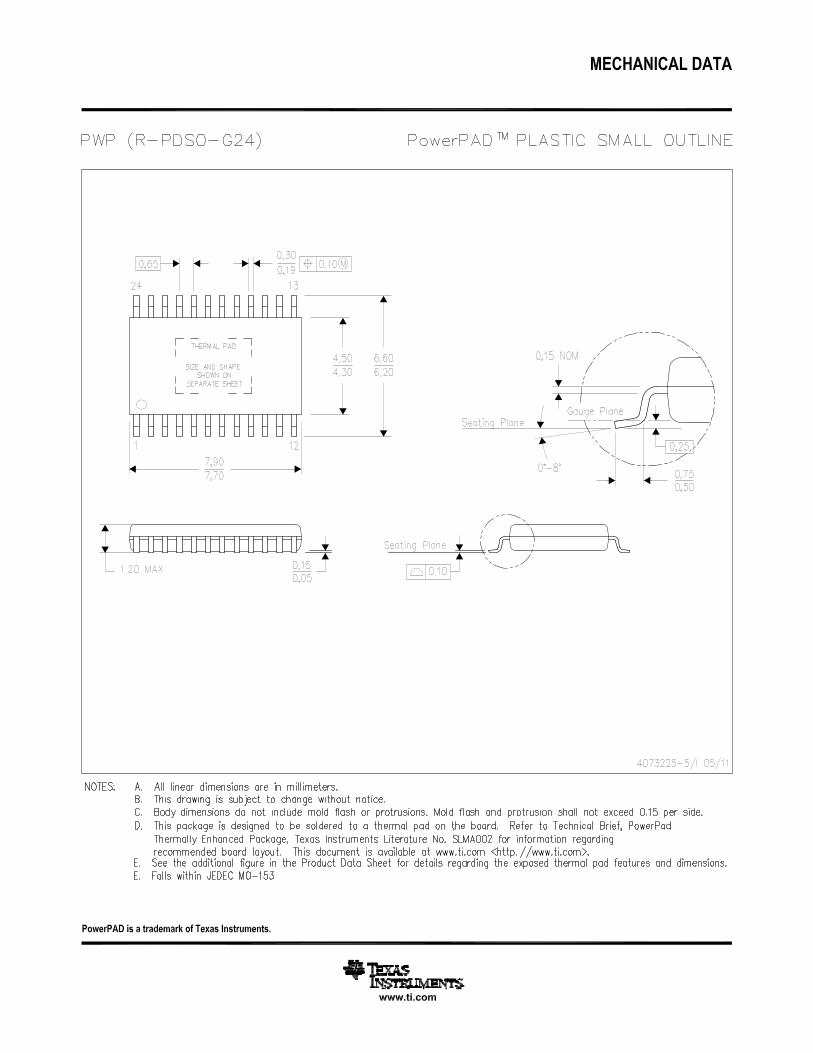
The thermally enhanced PWP package is based on the 24-pin TSSOP, but includes a thermal pad (see Figure 58)to provide an effective thermal contact between the IC and the PWB.
Traditionally, surface-mount and power have been mutually exclusive terms. A variety of scaled-down TO-220-typepackages have leads formed as gull wings to make them applicable for surface-mount applications. These packages,however, have only two shortcomings: they do not address the very low profile requirements (<2 mm) of many oftoday’s advanced systems, and they do not offer a terminal-count high enough to accommodate increasingintegration. On the other hand, traditional low-power surface-mount packages require power-dissipation derating thatseverely limits the usable range of many high-performance analog circuits.
The PowerPAD package (thermally enhanced TSSOP) combines fine-pitch surface-mount technology with thermalperformance comparable to much larger power packages.
The PowerPAD package is designed to optimize the heat transfer to the PWB. Because of the very small size andlimited mass of a TSSOP package, thermal enhancement is achieved by improving the thermal conduction paths thatremove heat from the component. The thermal pad is formed using a patented lead-frame design and manufacturingtechnique to provide a direct connection to the heat-generating IC. When this pad is soldered or otherwise thermallycoupled to an external heat dissipator, high power dissipation in the ultra-thin, fine-pitch, surface-mount package canbe reliably achieved.
DIE
Side View (a)
End View (b)
Bottom View (c)
DIE
ThermalPad
Figure 58. Views of Thermally Enhanced PWP Package
TPA02022-W STEREO AUDIO POWER AMPLIFIER
SLOS205B – FEBRUARY 1998 – REVISED DECEMBER 2000
24 POST OFFICE BOX 655303 • DALLAS, TEXAS 75265
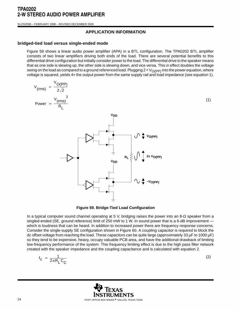
APPLICATION INFORMATION
bridged-tied load versus single-ended mode
Figure 59 shows a linear audio power amplifier (APA) in a BTL configuration. The TPA0202 BTL amplifierconsists of two linear amplifiers driving both ends of the load. There are several potential benefits to thisdifferential drive configuration but initially consider power to the load. The differential drive to the speaker meansthat as one side is slewing up, the other side is slewing down, and vice versa. This in effect doubles the voltageswing on the load as compared to a ground referenced load. Plugging 2 × VO(PP) into the power equation, wherevoltage is squared, yields 4× the output power from the same supply rail and load impedance (see equation 1).
Power V(rms)
2
RL
(1)
V(rms) VO(PP)
2 2
RL 2x VO(PP)
VO(PP)
–VO(PP)
VDD
VDD
Figure 59. Bridge-Tied Load Configuration
In a typical computer sound channel operating at 5 V, bridging raises the power into an 8-Ω speaker from asingled-ended (SE, ground reference) limit of 250 mW to 1 W. In sound power that is a 6-dB improvement —which is loudness that can be heard. In addition to increased power there are frequency response concerns.Consider the single-supply SE configuration shown in Figure 60. A coupling capacitor is required to block thedc offset voltage from reaching the load. These capacitors can be quite large (approximately 33 µF to 1000 µF)so they tend to be expensive, heavy, occupy valuable PCB area, and have the additional drawback of limitinglow-frequency performance of the system. This frequency limiting effect is due to the high pass filter networkcreated with the speaker impedance and the coupling capacitance and is calculated with equation 2.
fc 12RLCC
(2)

TPA02022-W STEREO AUDIO POWER AMPLIFIER
SLOS205B – FEBRUARY 1998 – REVISED DECEMBER 2000
25POST OFFICE BOX 655303 • DALLAS, TEXAS 75265
APPLICATION INFORMATION
bridged-tied load versus single-ended mode (continued)
For example, a 68-µF capacitor with an 8-Ω speaker would attenuate low frequencies below 293 Hz. The BTLconfiguration cancels the dc offsets, which eliminates the need for the blocking capacitors. Low-frequencyperformance is then limited only by the input network and speaker response. Cost and PCB space are alsominimized by eliminating the bulky coupling capacitor.
RL
CCVO(PP)
VO(PP)
VDD
–3 dB
fc
Figure 60. Single-Ended Configuration and Frequency Response
Increasing power to the load does carry a penalty of increased internal power dissipation. The increaseddissipation is understandable considering that the BTL configuration produces 4× the output power of the SEconfiguration. Internal dissipation versus output power is discussed further in the thermal considerationssection.
BTL amplifier efficiency
Linear amplifiers are notoriously inefficient. The primary cause of these inefficiencies is voltage drop across theoutput stage transistors. There are two components of the internal voltage drop. One is the headroom or dcvoltage drop that varies inversely to output power. The second component is due to the sinewave nature of theoutput. The total voltage drop can be calculated by subtracting the RMS value of the output voltage from VDD.The internal voltage drop multiplied by the RMS value of the supply current, IDDrms, determines the internalpower dissipation of the amplifier.
An easy-to-use equation to calculate efficiency starts out as being equal to the ratio of power from the powersupply to the power delivered to the load. To accurately calculate the RMS values of power in the load and inthe amplifier, the current and voltage waveform shapes must first be understood (see Figure 61).
V(LRMS)
VO IDD
IDD(RMS)
Figure 61. Voltage and Current Waveforms for BTL Amplifiers

TPA02022-W STEREO AUDIO POWER AMPLIFIER
SLOS205B – FEBRUARY 1998 – REVISED DECEMBER 2000
26 POST OFFICE BOX 655303 • DALLAS, TEXAS 75265
APPLICATION INFORMATION
Although the voltages and currents for SE and BTL are sinusoidal in the load, currents from the supply are verydifferent between SE and BTL configurations. In an SE application the current waveform is a half-wave rectifiedshape, whereas in BTL it is a full-wave rectified waveform. This means RMS conversion factors are different.Keep in mind that for most of the waveform both the push and pull transistors are not on at the same time, whichsupports the fact that each amplifier in the BTL device only draws current from the supply for half the waveform.The following equations are the basis for calculating amplifier efficiency.
IDDrms 2VP RL
PSUP VDD IDDrms VDD 2VP RL
Efficiency PL
PSUP
Efficiency of a BTL Configuration VP2VDD
PL
RL
212
2VDD
(3)
Where:
(4)
PL VLrms2
RL
Vp2
2RL
VLrms VP
2
Table 1 employs equation 4 to calculate efficiencies for four different output power levels. Note that the efficiencyof the amplifier is quite low for lower power levels and rises sharply as power to the load is increased resultingin a nearly flat internal power dissipation over the normal operating range. Note that the internal dissipation atfull output power is less than in the half power range. Calculating the efficiency for a specific system is the keyto proper power supply design. For a stereo 1-W audio system with 8-Ω loads and a 5-V supply, the maximumdraw on the power supply is almost 3.25 W.
Table 1. Efficiency Vs Output Power in 5-V 8-Ω BTL Systems
OUTPUT POWER(W)
EFFICIENCY(%)
PEAK-TO-PEAKVOLTAGE
(V)
INTERNAL DISSIPATION
(W)
0.25 31.4 2.00 0.55
0.50 44.4 2.83 0.62
1.00 62.8 4.00 0.59
1.25 70.2 4.47† 0.53
† High peak voltages cause the THD to increase.
A final point to remember about linear amplifiers (either SE or BTL) is how to manipulate the terms in theefficiency equation to utmost advantage when possible. Note that in equation 4, VDD is in the denominator. Thisindicates that as VDD goes down, efficiency goes up.
TPA02022-W STEREO AUDIO POWER AMPLIFIER
SLOS205B – FEBRUARY 1998 – REVISED DECEMBER 2000
27POST OFFICE BOX 655303 • DALLAS, TEXAS 75265
APPLICATION INFORMATION
For example, if the 5-V supply is replaced with a 3.3-V supply (TPA0202 has a maximum recommended VDDof 5.5 V) in the calculations of Table 1, then efficiency at 0.5 W would rise from 44% to 67% and internal powerdissipation would fall from 0.62 W to 0.25 W at 5 V. Then for a stereo 0.5-W system from a 3.3-V supply, themaximum draw would only be 1.5 W as compared to 2.24 W from 5 V. In other words, use the efficiency analysisto choose the correct supply voltage and speaker impedance for the application.
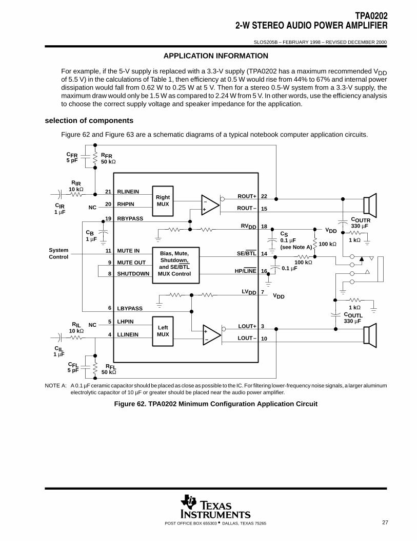
selection of components
Figure 62 and Figure 63 are a schematic diagrams of a typical notebook computer application circuits.
CB1 µF
CS0.1 µF(see Note A)
RightMUX
RLINEIN
RHPIN
LeftMUX
LHPIN
LLINEIN
Bias, Mute,Shutdown,and SE/BTLMUX Control
+–
+–
RBYPASS
MUTE IN
MUTE OUT
SHUTDOWN
LBYPASS
ROUT+
ROUT–
RVDD
LVDD
LOUT+
LOUT–
SE/BTL
HP/LINE
CIR1 µF
RIR10 kΩ
RFR50 kΩ
CFR5 pF
SystemControl
CIL1 µF
RIL10 kΩ
NC
NC
4
5
6
8
9
11
19
20
21
RFL50 kΩ
CFL5 pF
100 kΩ
100 kΩ
VDD
VDD
COUTR330 µF
COUTL330 µF
10
3
16
7
14
18
15
22
1 kΩ
1 kΩ
0.1 µF
NOTE A: A 0.1 µF ceramic capacitor should be placed as close as possible to the IC. For filtering lower-frequency noise signals, a larger aluminumelectrolytic capacitor of 10 µF or greater should be placed near the audio power amplifier.
Figure 62. TPA0202 Minimum Configuration Application Circuit

TPA02022-W STEREO AUDIO POWER AMPLIFIER
SLOS205B – FEBRUARY 1998 – REVISED DECEMBER 2000
28 POST OFFICE BOX 655303 • DALLAS, TEXAS 75265
APPLICATION INFORMATION
CBR0.1 µF CSR
0.1 µF(see Note B)
RightMUX
RLINEIN
RHPIN
LeftMUX
LHPIN
LLINEIN
Bias, Mute,Shutdown,and SE/BTLMUX Control
+–
+–
RBYPASS
MUTE IN
MUTE OUT
SHUTDOWN
LBYPASS
ROUT+
ROUT–
RVDD
LVDD
LOUT+
LOUT–
SE/BTL
HP/LINE
CIRLINE1 µF RIRLINE
10 kΩ
RFRLINE50 kΩ
CFRLINE5 pF
SystemControl
CILLINE1 µF
RILLINE10 kΩ
4
5
6
8
9
11
19
20
21
RFLLINE50 kΩ
CFLLINE5 pF
100 kΩ
100 kΩ
VDD
COUTR330 µF
COUTL330 µF
10
3
16
7
14
18
15
22
1 kΩ
CIRHP1 µF
RIRHP10 kΩ
RFRHP10 kΩ
See Note A
CBL1 µF
CILHP1 µF RILHP
10 kΩ
RFLHP10 kΩ
CSR0.1 µF(see Note B)
VDD
1 kΩ
0.1 µF
NOTES: A. This connection is for ultra-low current in shutdown mode.B. A 0.1 µF ceramic capacitor should be placed as close as possible to the IC. For filtering lower-frequency noise signals, a larger
aluminum electrolytic capacitor of 10 µF or greater should be placed near the audio power amplifier.
Figure 63. TPA0202 Full Configuration Application Circuit

TPA02022-W STEREO AUDIO POWER AMPLIFIER
SLOS205B – FEBRUARY 1998 – REVISED DECEMBER 2000
29POST OFFICE BOX 655303 • DALLAS, TEXAS 75265
APPLICATION INFORMATION
gain setting resistors, RF and RI
The gain for each audio input of the TPA0202 is set by resistors RF and RI according to equation 5 for BTL mode.
(5)BTL Gain 2RFRI
BTL mode operation brings about the factor 2 in the gain equation due to the inverting amplifier mirroring thevoltage swing across the load. Given that the TPA0202 is a MOS amplifier, the input impedance is very high,consequently input leakage currents are not generally a concern although noise in the circuit increases as thevalue of RF increases. In addition, a certain range of RF values is required for proper start-up operation of theamplifier. Taken together it is recommended that the effective impedance seen by the inverting node of theamplifier be set between 5 kΩ and 20 kΩ. The effective impedance is calculated in equation 6.
(6)Effective Impedance RFRI
RF RI
As an example consider an input resistance of 10 kΩ and a feedback resistor of 50 kΩ. The BTL gain of theamplifier would be –10 and the effective impedance at the inverting terminal would be 8.3 kΩ, which is well withinthe recommended range.
For high performance applications metal film resistors are recommended because they tend to have lower noiselevels than carbon resistors. For values of RF above 50 kΩ the amplifier tends to become unstable due to a poleformed from RF and the inherent input capacitance of the MOS input structure. For this reason, a smallcompensation capacitor of approximately 5 pF should be placed in parallel with RF when RF is greater than50 kΩ. This, in effect, creates a low pass filter network with the cutoff frequency defined in equation 7.
(7)fc(lowpass) 1
2RFCF
–3 dB
fc
For example, if RF is 100 kΩ and Cf is 5 pF then fc is 318 kHz, which is well outside of the audio range.
TPA02022-W STEREO AUDIO POWER AMPLIFIER
SLOS205B – FEBRUARY 1998 – REVISED DECEMBER 2000
30 POST OFFICE BOX 655303 • DALLAS, TEXAS 75265
APPLICATION INFORMATION
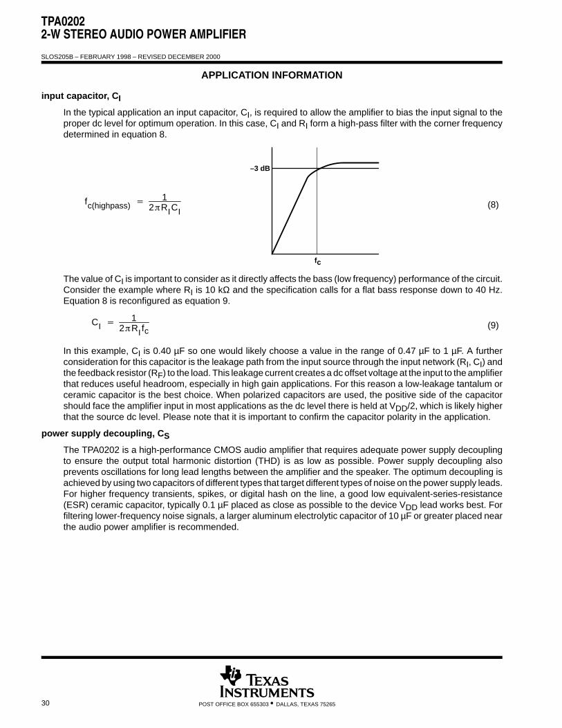
input capacitor, CI
In the typical application an input capacitor, CI, is required to allow the amplifier to bias the input signal to theproper dc level for optimum operation. In this case, CI and RI form a high-pass filter with the corner frequencydetermined in equation 8.
(8)
–3 dB
fc
fc(highpass) 1
2RICI
The value of CI is important to consider as it directly affects the bass (low frequency) performance of the circuit.Consider the example where RI is 10 kΩ and the specification calls for a flat bass response down to 40 Hz.Equation 8 is reconfigured as equation 9.
(9)CI 1
2RIfc
In this example, CI is 0.40 µF so one would likely choose a value in the range of 0.47 µF to 1 µF. A furtherconsideration for this capacitor is the leakage path from the input source through the input network (RI, CI) andthe feedback resistor (RF) to the load. This leakage current creates a dc offset voltage at the input to the amplifierthat reduces useful headroom, especially in high gain applications. For this reason a low-leakage tantalum orceramic capacitor is the best choice. When polarized capacitors are used, the positive side of the capacitorshould face the amplifier input in most applications as the dc level there is held at VDD/2, which is likely higherthat the source dc level. Please note that it is important to confirm the capacitor polarity in the application.
power supply decoupling, CS
The TPA0202 is a high-performance CMOS audio amplifier that requires adequate power supply decouplingto ensure the output total harmonic distortion (THD) is as low as possible. Power supply decoupling alsoprevents oscillations for long lead lengths between the amplifier and the speaker. The optimum decoupling isachieved by using two capacitors of different types that target different types of noise on the power supply leads.For higher frequency transients, spikes, or digital hash on the line, a good low equivalent-series-resistance(ESR) ceramic capacitor, typically 0.1 µF placed as close as possible to the device VDD lead works best. Forfiltering lower-frequency noise signals, a larger aluminum electrolytic capacitor of 10 µF or greater placed nearthe audio power amplifier is recommended.

TPA02022-W STEREO AUDIO POWER AMPLIFIER
SLOS205B – FEBRUARY 1998 – REVISED DECEMBER 2000
31POST OFFICE BOX 655303 • DALLAS, TEXAS 75265
APPLICATION INFORMATION
midrail bypass capacitor, CB
The midrail bypass capacitor, CB, is the most critical capacitor and serves several important functions. Duringstartup or recovery from shutdown mode, CB determines the rate at which the amplifier starts up. The secondfunction is to reduce noise produced by the power supply caused by coupling into the output drive signal. Thisnoise is from the midrail generation circuit internal to the amplifier, which appears as degraded PSRR andTHD+N. The capacitor is fed from a 100-kΩ source inside the amplifier. To keep the start-up pop as low aspossible, the relationship shown in equation 10 should be maintained.
(10)1
CB 100 kΩ 1
CIRI RF
As an example, consider a circuit where CB is 1 µF, CI is 0.22 µF, RF is 50 kΩ, and RI is 10 kΩ. Inserting thesevalues into the equation 10 we get 10 ≤ 75, which satisfies the rule. Bypass capacitor, CB, values of 0.1 µF to1 µF ceramic or tantalum low-ESR capacitors are recommended for the best THD and noise performance.
In Figure 63, the full feature configuration, two bypass capacitors are used. This provides the maximumseparation between right and left drive circuits. When absolute minimum cost and/or component space isrequired, one bypass capacitor can be used as shown in Figure 62. It is critical that terminals 6 and 19 be tiedtogether in this configuration.
load considerations
Extremely low impedance loads (below 4 Ω) coupled with certain external component selections, board layouts,and cabling can cause oscillations in the system. Using a single air-cored inductor in series with the loadeliminates any spurious oscillations that might occur. An inductance of approximately 1 µH has been shown toeliminate such oscillations. There are no special considerations when using 4 Ω and above loads with thisamplifier.
optimizing depop operation
Circuitry has been included in the TPA0202 to minimize the amount of popping heard at power-up and whencoming out of shutdown mode. Popping occurs whenever a voltage step is applied to the speaker. If highimpedances are used for the feedback and input resistors, it is possible for the input capacitor to drift downwardsfrom mid-rail during mute and shutdown. A high gain amplifier intensifies the problem as the small delta involtage is multiplied by the gain. So it is advantageous to use low-gain configurations, and to limit the size ofthe gain-setting resistors. The time constant of the input coupling capacitor (CI) and the gain-setting resistors(RI and RF) needs to be shorter than the time constant formed by the bypass capacitor (CB) and the outputimpedance of the mid-rail generator, which is nominally 100 kΩ (see equation 10).
The effective output impedance of the mid-rail generator is actually greater than 100 kΩ due to a PNP transistorclamping the input node (see Figure 64).

TPA02022-W STEREO AUDIO POWER AMPLIFIER
SLOS205B – FEBRUARY 1998 – REVISED DECEMBER 2000
32 POST OFFICE BOX 655303 • DALLAS, TEXAS 75265
APPLICATION INFORMATION
50 kΩBYPASS
VDD
100 kΩ
100 kΩ
Figure 64. PNP Transistor Clamping of BYPASS Terminal
The PNP transistor limits the voltage drop across the 50 kΩ resistor by slewing the internal node slowly whenpower is applied. At start-up, the xBYPASS capacitor is at 0. The PNP is pulling the mid-point of the bias circuitdown, so the capacitor sees a lower effective voltage, and thus charges slower. This appears as a linear ramp(while the PNP transistor is conducting), followed by the expected exponential ramp of an R-C circuit.
If the expression in equation 10 cannot be fulfilled or the small amount of pop is still unacceptable for theapplication, then external circuitry must be added that can eliminate the pop heard during power up and whiletransitioning out of mute or shutdown modes.
By holding the device in SE mode when the pop normally occurs, no pop can be heard through theBTL-connected speakers (as the negative output is in a high impedance state when the amplifier is in SE mode).
From a hardware point of view, the easiest way to implement this is to drive the SE/BTL terminal from thegeneral-purpose input-output (GPIO) in the system. If the SE/BTL terminal is normally connected to aheadphone socket (as shown in Figure 65), then the GPIO signal must either be taken through an OR gate (seeFigure 65) or isolated with a diode (any signal diode) (see Figure 66).
Rm2100 kΩ
Rm1100 kΩ
VDD
Left ChannelFrom GPIO
RightChannel
SE/BTL 0.1 µF
Figure 65. Implementation with an OR Gate

TPA02022-W STEREO AUDIO POWER AMPLIFIER
SLOS205B – FEBRUARY 1998 – REVISED DECEMBER 2000
33POST OFFICE BOX 655303 • DALLAS, TEXAS 75265
APPLICATION INFORMATION
SE/BTLRm2100 kΩ
Rm1100 kΩ
VDD
LeftChannel
From GPIO
RightChannel
0.1 µF
Figure 66. Implementation with a Diode
The OR gate and diode isolate the GPIO terminal from the headphone switch. In these implementations, theheadphone switch has priority.
When the amplifier is in mute mode, the output stage continues to be biased. This causes the transition out ofmute mode to be very fast with only a short delay (from 100 ms to 500 ms). During power up or the transitionout of shutdown mode, a longer delay ( from 1 s to 2 s) is required. The exact delay time required is dependenton the values of the external components used with the amplifier (see Figure 67).
System Control:MUTE or SHUTDOWN
Delay
Output of Delay Circuit(Input to SE/BTL)
Figure 67. Transition Delay Timing
single-ended operation
In SE mode (see Figure 59 and Figure 60), the load is driven from the primary amplifier output for each channel(OUT+, terminals 22 and 3).
In SE mode the gain is set by the RF and RI resistors and is shown in equation 11. Since the inverting amplifieris not used to mirror the voltage swing on the load, the factor of 2, from equation 5, is not included.
(11)SE Gain RFRI
The output coupling capacitor required in single-supply SE mode also places additional constraints on theselection of other components in the amplifier circuit. The rules described earlier still hold with the addition ofthe following relationship (see equation 12):
(12)1
CB 25 kΩ 1CIRI
1
RLCC

TPA02022-W STEREO AUDIO POWER AMPLIFIER
SLOS205B – FEBRUARY 1998 – REVISED DECEMBER 2000
34 POST OFFICE BOX 655303 • DALLAS, TEXAS 75265
APPLICATION INFORMATION
output coupling capacitor, CC
In the typical single-supply SE configuration, an output coupling capacitor (CC) is required to block the dc biasat the output of the amplifier thus preventing dc currents in the load. As with the input coupling capacitor, theoutput coupling capacitor and impedance of the load form a high-pass filter governed by equation 14.
(14)fc(high) 1
2RLCC
–3 dB
fc
The main disadvantage, from a performance standpoint, is the load impedances are typically small, which drivesthe low-frequency corner higher degrading the bass response. Large values of CC are required to pass lowfrequencies into the load. Consider the example where a CC of 330 µF is chosen and loads vary from 3 Ω,4 Ω, 8 Ω, 32 Ω, 10 kΩ, to 47 kΩ. Table 2 summarizes the frequency response characteristics of eachconfiguration.
Table 2. Common Load Impedances Vs Low Frequency Output Characteristics in SE Mode
RL CC LOWEST FREQUENCY
3 Ω 330 µF 161 Hz
4 Ω 330 µF 120 Hz
8 Ω 330 µF 60 Hz
32 Ω 330 µF 15 Hz
10,000 Ω 330 µF 0.05 Hz
47,000 Ω 330 µF 0.01 Hz
As Table 2 indicates, most of the bass response is attenuated into a 4-Ω load, an 8-Ω load is adequate,headphone response is good, and drive into line level inputs (a home stereo for example) is exceptional.
TPA02022-W STEREO AUDIO POWER AMPLIFIER
SLOS205B – FEBRUARY 1998 – REVISED DECEMBER 2000
35POST OFFICE BOX 655303 • DALLAS, TEXAS 75265
APPLICATION INFORMATION
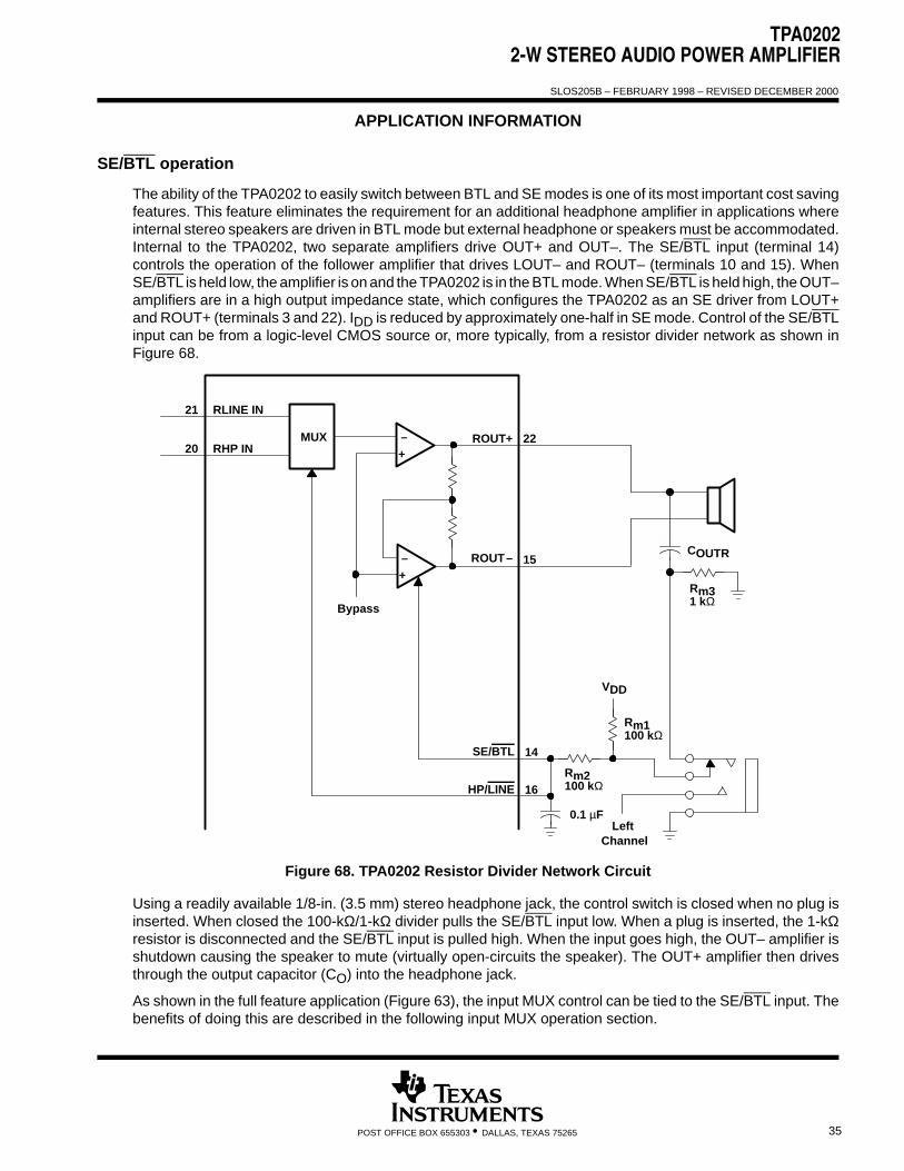
SE/BTL operation
The ability of the TPA0202 to easily switch between BTL and SE modes is one of its most important cost savingfeatures. This feature eliminates the requirement for an additional headphone amplifier in applications whereinternal stereo speakers are driven in BTL mode but external headphone or speakers must be accommodated.Internal to the TPA0202, two separate amplifiers drive OUT+ and OUT–. The SE/BTL input (terminal 14)controls the operation of the follower amplifier that drives LOUT– and ROUT– (terminals 10 and 15). WhenSE/BTL is held low, the amplifier is on and the TPA0202 is in the BTL mode. When SE/BTL is held high, the OUT–amplifiers are in a high output impedance state, which configures the TPA0202 as an SE driver from LOUT+and ROUT+ (terminals 3 and 22). IDD is reduced by approximately one-half in SE mode. Control of the SE/BTLinput can be from a logic-level CMOS source or, more typically, from a resistor divider network as shown inFigure 68.
MUX
RLINE IN
RHP IN +–
Bypass
SE/BTL
HP/LINERm2100 kΩ
Rm1100 kΩ
VDD
COUTR
16
14
Rm31 kΩ
+– ROUT– 15
ROUT+ 22
Left Channel
20
21
0.1 µF
Figure 68. TPA0202 Resistor Divider Network Circuit
Using a readily available 1/8-in. (3.5 mm) stereo headphone jack, the control switch is closed when no plug isinserted. When closed the 100-kΩ/1-kΩ divider pulls the SE/BTL input low. When a plug is inserted, the 1-kΩresistor is disconnected and the SE/BTL input is pulled high. When the input goes high, the OUT– amplifier isshutdown causing the speaker to mute (virtually open-circuits the speaker). The OUT+ amplifier then drivesthrough the output capacitor (CO) into the headphone jack.
As shown in the full feature application (Figure 63), the input MUX control can be tied to the SE/BTL input. Thebenefits of doing this are described in the following input MUX operation section.

TPA02022-W STEREO AUDIO POWER AMPLIFIER
SLOS205B – FEBRUARY 1998 – REVISED DECEMBER 2000
36 POST OFFICE BOX 655303 • DALLAS, TEXAS 75265
APPLICATION INFORMATION
Input MUX operation
Working in concert with the SE/BTL feature, the HP/LINE MUX feature gives the audio designer the flexibilityof a multichip design in a single IC (see Figure 69). The primary function of the MUX is to allow different gainsettings for BTL versus SE mode. Speakers typically require approximately a factor of 10 more gain for similarvolume listening levels as compared to headphones. To achieve headphone and speaker listening parity, theresistor values would need to be set as follows:
(15)SE Gain(HP) RF(HP)RI(HP)
If, for example RI(HP) = 10 kΩ and RF(HP) = 10 kΩ then SE Gain(HP) = –1
(16)BTL Gain(LINE) 2 RF(LINE)RI(LINE)
If, for example RI(LINE) = 10 kΩ and RF(LINE) = 50 kΩ then BTL Gain(LINE) = –10
ROUT+
ROUT–
CIRLINE RIRLINE
15
22
CIRHPRIRHP
RFRHP
MUX
RLINE IN
RHP IN
SE/BTL
HP/LINE
VDD
16
14
+–
Left Channel
20
21
Right ChannelMID
RFRLINE
0.1 µF
Figure 69. TPA0202 Example Input MUX Circuit
Another advantage of using the MUX feature is setting the gain of the headphone channel to –1. This providesthe optimum distortion performance into the headphones where clear sound is more important. Refer to theSE/BTL operation section for a description of the headphone jack control circuit.

TPA02022-W STEREO AUDIO POWER AMPLIFIER
SLOS205B – FEBRUARY 1998 – REVISED DECEMBER 2000
37POST OFFICE BOX 655303 • DALLAS, TEXAS 75265
APPLICATION INFORMATION
mute and shutdown modes
The TPA0202 employs both a mute and a shutdown mode of operation designed to reduce supply current, IDD,to the absolute minimum level during periods of nonuse for battery-power conservation. The SHUTDOWN inputterminal should be held low during normal operation when the amplifier is in use. Pulling SHUTDOWN highcauses the outputs to mute and the amplifier to enter a low-current state, IDD = 5 µA. SHUTDOWN or MUTEIN should never be left unconnected because amplifier operation would be unpredictable. Mute mode alonereduces IDD to 1.5 mA.
Table 3. Shutdown and Mute Mode Functions
INPUTS† OUTPUT AMPLIFIER STATE
SE/BTL HP/LINE MUTE IN SHUTDOWN MUTE OUT INPUT OUTPUT
Low Low Low Low Low L/R Line BTL
X X — High — X Mute
X X High — High X Mute
Low High Low Low Low L/R HP BTL
High Low Low Low Low L/R Line SE
High High Low Low Low L/R HP SE
† Inputs should never be left unconnected.X = do not care
using low-ESR capacitors
Low-ESR capacitors are recommended throughout this applications section. A real (as opposed to ideal)capacitor can be modeled simply as a resistor in series with an ideal capacitor. The voltage drop across thisresistor minimizes the beneficial effects of the capacitor in the circuit. The lower the equivalent value of thisresistance the more the real capacitor behaves like an ideal capacitor.
5-V versus 3.3-V operation
The TPA0202 operates over a supply range of 3 V to 5.5 V. This data sheet provides full specifications for 5-Vand 3.3-V operation, as these are considered to be the two most common standard voltages. There are nospecial considerations for 3.3-V versus 5-V operation as far as supply bypassing, gain setting, or stability goes.For 3.3-V operation, supply current is reduced from 19 mA (typical) to 13 mA (typical). The most importantconsideration is that of output power. Each amplifier in TPA0202 can produce a maximum voltage swing ofVDD – 1 V. This means, for 3.3-V operation, clipping starts to occur when VO(PP) = 2.3 V as opposed toVO(PP) = 4 V at 5 V. The reduced voltage swing subsequently reduces maximum output power into an 8-Ω loadbefore distortion becomes significant.
Operation from 3.3-V supplies, as can be shown from the efficiency formula in equation 4, consumesapproximately two-thirds the supply power for a given output-power level than operation from 5-V supplies.When the application demands less than 500 mW, 3.3-V operation should be strongly considered, especiallyin battery-powered applications to improve the efficiency.

TPA02022-W STEREO AUDIO POWER AMPLIFIER
SLOS205B – FEBRUARY 1998 – REVISED DECEMBER 2000
38 POST OFFICE BOX 655303 • DALLAS, TEXAS 75265
APPLICATION INFORMATION
headroom and thermal considerations
Linear power amplifiers dissipate a significant amount of heat in the package under normal operating conditions.A typical music CD requires 12 dB to 15 dB of dynamic headroom to pass the loudest portions without distortionas compared with the average power output. From the TPA0202 data sheet, one can see that when theTPA0202 is operating from a 5-V supply into a 3-Ω speaker that 2 W peaks are available. Converting watts todB:
PdB 10Log PWPref
10Log21
3.0 dB
(17)
Subtracting the headroom restriction to obtain the average listening level without distortion yields:
3.0 dB 15 dB 12 dB (15 dB headroom)
3.0 dB 12 dB 9 dB (12 dB headroom)
3.0 dB 9 dB 6 dB (9 dB headroom)
3.0 dB 6 dB 3 dB (6 dB headroom)
3.0 dB 3 dB 0 dB (3 dB headroom)
Converting dB back into watts:
PW 10PdB10 Pref
63 mW (15 dB headroom)
120 mW (12 dB headroom)
250 mW (9 dB headroom)
500 mW (6 dB headroom)
1000 mW (3 dB headroom)
(18)
This is valuable information to consider when attempting to estimate the heat dissipation requirements for theamplifier system. Comparing the absolute worst case, which is 2 W of continuous power output with 0 dB ofheadroom, against 12 dB and 15 dB applications drastically affects maximum ambient temperature ratings forthe system. Using the power dissipation curves for a 5-V, 3-Ω system, the internal dissipation in the TPA0202and maximum ambient temperatures is shown in Table 4.
TPA02022-W STEREO AUDIO POWER AMPLIFIER
SLOS205B – FEBRUARY 1998 – REVISED DECEMBER 2000
39POST OFFICE BOX 655303 • DALLAS, TEXAS 75265
APPLICATION INFORMATION
headroom and thermal considerations (continued)
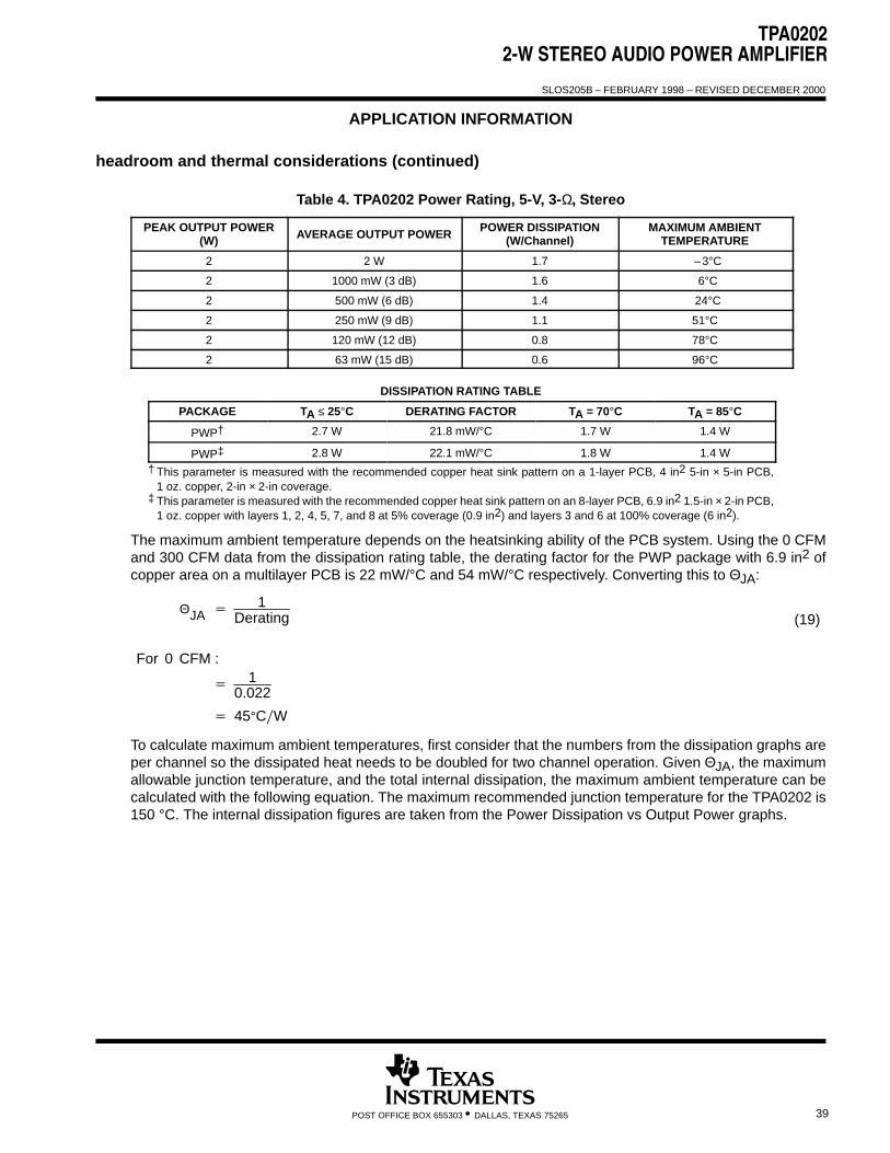
Table 4. TPA0202 Power Rating, 5-V, 3-Ω, Stereo
PEAK OUTPUT POWER(W) AVERAGE OUTPUT POWER
POWER DISSIPATION(W/Channel)
MAXIMUM AMBIENTTEMPERATURE
2 2 W 1.7 –3°C
2 1000 mW (3 dB) 1.6 6°C
2 500 mW (6 dB) 1.4 24°C
2 250 mW (9 dB) 1.1 51°C
2 120 mW (12 dB) 0.8 78°C
2 63 mW (15 dB) 0.6 96°C
DISSIPATION RATING TABLE
PACKAGE TA ≤ 25°CÁÁÁÁÁÁÁÁÁÁÁÁÁÁDERATING FACTOR TA = 70°C TA = 85°CÁÁÁÁÁÁ
ÁÁÁÁÁÁPWP†ÁÁÁÁÁÁÁÁÁÁÁÁÁÁ
2.7 WÁÁÁÁÁÁÁÁÁÁÁÁÁÁ
21.8 mW/°CÁÁÁÁÁÁÁÁÁÁÁÁÁÁ
1.7 WÁÁÁÁÁÁÁÁÁÁÁÁ
1.4 W
PWP‡ 2.8 WÁÁÁÁÁÁÁÁÁÁÁÁÁÁ
22.1 mW/°C 1.8 W 1.4 W† This parameter is measured with the recommended copper heat sink pattern on a 1-layer PCB, 4 in2 5-in × 5-in PCB,
1 oz. copper, 2-in × 2-in coverage.‡ This parameter is measured with the recommended copper heat sink pattern on an 8-layer PCB, 6.9 in2 1.5-in × 2-in PCB,
1 oz. copper with layers 1, 2, 4, 5, 7, and 8 at 5% coverage (0.9 in2) and layers 3 and 6 at 100% coverage (6 in2).
The maximum ambient temperature depends on the heatsinking ability of the PCB system. Using the 0 CFMand 300 CFM data from the dissipation rating table, the derating factor for the PWP package with 6.9 in2 ofcopper area on a multilayer PCB is 22 mW/°C and 54 mW/°C respectively. Converting this to ΘJA:
ΘJA 1
Derating
10.022
45°CW
For 0 CFM :
(19)
To calculate maximum ambient temperatures, first consider that the numbers from the dissipation graphs areper channel so the dissipated heat needs to be doubled for two channel operation. Given ΘJA, the maximumallowable junction temperature, and the total internal dissipation, the maximum ambient temperature can becalculated with the following equation. The maximum recommended junction temperature for the TPA0202 is150 °C. The internal dissipation figures are taken from the Power Dissipation vs Output Power graphs.
TPA02022-W STEREO AUDIO POWER AMPLIFIER
SLOS205B – FEBRUARY 1998 – REVISED DECEMBER 2000
40 POST OFFICE BOX 655303 • DALLAS, TEXAS 75265
APPLICATION INFORMATION
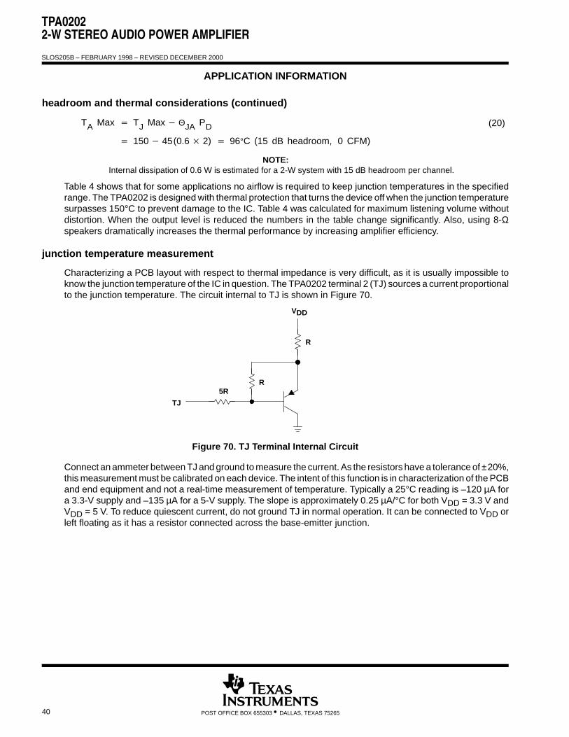
headroom and thermal considerations (continued)
TA Max TJ Max ΘJA PD
150 45(0.6 2) 96°C (15 dB headroom, 0 CFM)
(20)
NOTE:Internal dissipation of 0.6 W is estimated for a 2-W system with 15 dB headroom per channel.
Table 4 shows that for some applications no airflow is required to keep junction temperatures in the specifiedrange. The TPA0202 is designed with thermal protection that turns the device off when the junction temperaturesurpasses 150°C to prevent damage to the IC. Table 4 was calculated for maximum listening volume withoutdistortion. When the output level is reduced the numbers in the table change significantly. Also, using 8-Ωspeakers dramatically increases the thermal performance by increasing amplifier efficiency.
junction temperature measurement
Characterizing a PCB layout with respect to thermal impedance is very difficult, as it is usually impossible toknow the junction temperature of the IC in question. The TPA0202 terminal 2 (TJ) sources a current proportionalto the junction temperature. The circuit internal to TJ is shown in Figure 70.
5R
TJ
VDD
R
R
Figure 70. TJ Terminal Internal Circuit
Connect an ammeter between TJ and ground to measure the current. As the resistors have a tolerance of ±20%,this measurement must be calibrated on each device. The intent of this function is in characterization of the PCBand end equipment and not a real-time measurement of temperature. Typically a 25°C reading is –120 µA fora 3.3-V supply and –135 µA for a 5-V supply. The slope is approximately 0.25 µA/°C for both VDD = 3.3 V andVDD = 5 V. To reduce quiescent current, do not ground TJ in normal operation. It can be connected to VDD orleft floating as it has a resistor connected across the base-emitter junction.
PACKAGE OPTION ADDENDUM
www.ti.com 15-Apr-2017
Addendum-Page 1
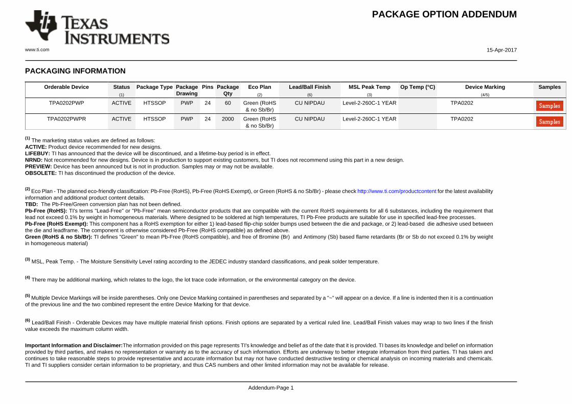
PACKAGING INFORMATION
Orderable Device Status(1)
Package Type PackageDrawing
Pins PackageQty
Eco Plan(2)
Lead/Ball Finish(6)
MSL Peak Temp(3)
Op Temp (°C) Device Marking(4/5)
Samples
TPA0202PWP ACTIVE HTSSOP PWP 24 60 Green (RoHS& no Sb/Br)
CU NIPDAU Level-2-260C-1 YEAR TPA0202
TPA0202PWPR ACTIVE HTSSOP PWP 24 2000 Green (RoHS& no Sb/Br)
CU NIPDAU Level-2-260C-1 YEAR TPA0202
(1) The marketing status values are defined as follows:ACTIVE: Product device recommended for new designs.LIFEBUY: TI has announced that the device will be discontinued, and a lifetime-buy period is in effect.NRND: Not recommended for new designs. Device is in production to support existing customers, but TI does not recommend using this part in a new design.PREVIEW: Device has been announced but is not in production. Samples may or may not be available.OBSOLETE: TI has discontinued the production of the device.
(2) Eco Plan - The planned eco-friendly classification: Pb-Free (RoHS), Pb-Free (RoHS Exempt), or Green (RoHS & no Sb/Br) - please check http://www.ti.com/productcontent for the latest availabilityinformation and additional product content details.TBD: The Pb-Free/Green conversion plan has not been defined.Pb-Free (RoHS): TI's terms "Lead-Free" or "Pb-Free" mean semiconductor products that are compatible with the current RoHS requirements for all 6 substances, including the requirement thatlead not exceed 0.1% by weight in homogeneous materials. Where designed to be soldered at high temperatures, TI Pb-Free products are suitable for use in specified lead-free processes.Pb-Free (RoHS Exempt): This component has a RoHS exemption for either 1) lead-based flip-chip solder bumps used between the die and package, or 2) lead-based die adhesive used betweenthe die and leadframe. The component is otherwise considered Pb-Free (RoHS compatible) as defined above.Green (RoHS & no Sb/Br): TI defines "Green" to mean Pb-Free (RoHS compatible), and free of Bromine (Br) and Antimony (Sb) based flame retardants (Br or Sb do not exceed 0.1% by weightin homogeneous material)
(3) MSL, Peak Temp. - The Moisture Sensitivity Level rating according to the JEDEC industry standard classifications, and peak solder temperature.
(4) There may be additional marking, which relates to the logo, the lot trace code information, or the environmental category on the device.
(5) Multiple Device Markings will be inside parentheses. Only one Device Marking contained in parentheses and separated by a "~" will appear on a device. If a line is indented then it is a continuationof the previous line and the two combined represent the entire Device Marking for that device.
(6) Lead/Ball Finish - Orderable Devices may have multiple material finish options. Finish options are separated by a vertical ruled line. Lead/Ball Finish values may wrap to two lines if the finishvalue exceeds the maximum column width.
Important Information and Disclaimer:The information provided on this page represents TI's knowledge and belief as of the date that it is provided. TI bases its knowledge and belief on informationprovided by third parties, and makes no representation or warranty as to the accuracy of such information. Efforts are underway to better integrate information from third parties. TI has taken andcontinues to take reasonable steps to provide representative and accurate information but may not have conducted destructive testing or chemical analysis on incoming materials and chemicals.TI and TI suppliers consider certain information to be proprietary, and thus CAS numbers and other limited information may not be available for release.

PACKAGE OPTION ADDENDUM
www.ti.com 15-Apr-2017
Addendum-Page 2
In no event shall TI's liability arising out of such information exceed the total purchase price of the TI part(s) at issue in this document sold by TI to Customer on an annual basis.

TAPE AND REEL INFORMATION
*All dimensions are nominal
Device PackageType
PackageDrawing
Pins SPQ ReelDiameter
(mm)
ReelWidth
W1 (mm)
A0(mm)
B0(mm)
K0(mm)
P1(mm)
W(mm)
Pin1Quadrant
TPA0202PWPR HTSSOP PWP 24 2000 330.0 16.4 6.95 8.3 1.6 8.0 16.0 Q1
PACKAGE MATERIALS INFORMATION
www.ti.com 1-May-2018
Pack Materials-Page 1

*All dimensions are nominal
Device Package Type Package Drawing Pins SPQ Length (mm) Width (mm) Height (mm)
TPA0202PWPR HTSSOP PWP 24 2000 367.0 367.0 38.0
PACKAGE MATERIALS INFORMATION
www.ti.com 1-May-2018
Pack Materials-Page 2

IMPORTANT NOTICE
Texas Instruments Incorporated (TI) reserves the right to make corrections, enhancements, improvements and other changes to itssemiconductor products and services per JESD46, latest issue, and to discontinue any product or service per JESD48, latest issue. Buyersshould obtain the latest relevant information before placing orders and should verify that such information is current and complete.TI’s published terms of sale for semiconductor products (http://www.ti.com/sc/docs/stdterms.htm) apply to the sale of packaged integratedcircuit products that TI has qualified and released to market. Additional terms may apply to the use or sale of other types of TI products andservices.Reproduction of significant portions of TI information in TI data sheets is permissible only if reproduction is without alteration and isaccompanied by all associated warranties, conditions, limitations, and notices. TI is not responsible or liable for such reproduceddocumentation. Information of third parties may be subject to additional restrictions. Resale of TI products or services with statementsdifferent from or beyond the parameters stated by TI for that product or service voids all express and any implied warranties for theassociated TI product or service and is an unfair and deceptive business practice. TI is not responsible or liable for any such statements.Buyers and others who are developing systems that incorporate TI products (collectively, “Designers”) understand and agree that Designersremain responsible for using their independent analysis, evaluation and judgment in designing their applications and that Designers havefull and exclusive responsibility to assure the safety of Designers' applications and compliance of their applications (and of all TI productsused in or for Designers’ applications) with all applicable regulations, laws and other applicable requirements. Designer represents that, withrespect to their applications, Designer has all the necessary expertise to create and implement safeguards that (1) anticipate dangerousconsequences of failures, (2) monitor failures and their consequences, and (3) lessen the likelihood of failures that might cause harm andtake appropriate actions. Designer agrees that prior to using or distributing any applications that include TI products, Designer willthoroughly test such applications and the functionality of such TI products as used in such applications.TI’s provision of technical, application or other design advice, quality characterization, reliability data or other services or information,including, but not limited to, reference designs and materials relating to evaluation modules, (collectively, “TI Resources”) are intended toassist designers who are developing applications that incorporate TI products; by downloading, accessing or using TI Resources in anyway, Designer (individually or, if Designer is acting on behalf of a company, Designer’s company) agrees to use any particular TI Resourcesolely for this purpose and subject to the terms of this Notice.TI’s provision of TI Resources does not expand or otherwise alter TI’s applicable published warranties or warranty disclaimers for TIproducts, and no additional obligations or liabilities arise from TI providing such TI Resources. TI reserves the right to make corrections,enhancements, improvements and other changes to its TI Resources. TI has not conducted any testing other than that specificallydescribed in the published documentation for a particular TI Resource.Designer is authorized to use, copy and modify any individual TI Resource only in connection with the development of applications thatinclude the TI product(s) identified in such TI Resource. NO OTHER LICENSE, EXPRESS OR IMPLIED, BY ESTOPPEL OR OTHERWISETO ANY OTHER TI INTELLECTUAL PROPERTY RIGHT, AND NO LICENSE TO ANY TECHNOLOGY OR INTELLECTUAL PROPERTYRIGHT OF TI OR ANY THIRD PARTY IS GRANTED HEREIN, including but not limited to any patent right, copyright, mask work right, orother intellectual property right relating to any combination, machine, or process in which TI products or services are used. Informationregarding or referencing third-party products or services does not constitute a license to use such products or services, or a warranty orendorsement thereof. Use of TI Resources may require a license from a third party under the patents or other intellectual property of thethird party, or a license from TI under the patents or other intellectual property of TI.TI RESOURCES ARE PROVIDED “AS IS” AND WITH ALL FAULTS. TI DISCLAIMS ALL OTHER WARRANTIES ORREPRESENTATIONS, EXPRESS OR IMPLIED, REGARDING RESOURCES OR USE THEREOF, INCLUDING BUT NOT LIMITED TOACCURACY OR COMPLETENESS, TITLE, ANY EPIDEMIC FAILURE WARRANTY AND ANY IMPLIED WARRANTIES OFMERCHANTABILITY, FITNESS FOR A PARTICULAR PURPOSE, AND NON-INFRINGEMENT OF ANY THIRD PARTY INTELLECTUALPROPERTY RIGHTS. TI SHALL NOT BE LIABLE FOR AND SHALL NOT DEFEND OR INDEMNIFY DESIGNER AGAINST ANY CLAIM,INCLUDING BUT NOT LIMITED TO ANY INFRINGEMENT CLAIM THAT RELATES TO OR IS BASED ON ANY COMBINATION OFPRODUCTS EVEN IF DESCRIBED IN TI RESOURCES OR OTHERWISE. IN NO EVENT SHALL TI BE LIABLE FOR ANY ACTUAL,DIRECT, SPECIAL, COLLATERAL, INDIRECT, PUNITIVE, INCIDENTAL, CONSEQUENTIAL OR EXEMPLARY DAMAGES INCONNECTION WITH OR ARISING OUT OF TI RESOURCES OR USE THEREOF, AND REGARDLESS OF WHETHER TI HAS BEENADVISED OF THE POSSIBILITY OF SUCH DAMAGES.Unless TI has explicitly designated an individual product as meeting the requirements of a particular industry standard (e.g., ISO/TS 16949and ISO 26262), TI is not responsible for any failure to meet such industry standard requirements.Where TI specifically promotes products as facilitating functional safety or as compliant with industry functional safety standards, suchproducts are intended to help enable customers to design and create their own applications that meet applicable functional safety standardsand requirements. Using products in an application does not by itself establish any safety features in the application. Designers mustensure compliance with safety-related requirements and standards applicable to their applications. Designer may not use any TI products inlife-critical medical equipment unless authorized officers of the parties have executed a special contract specifically governing such use.Life-critical medical equipment is medical equipment where failure of such equipment would cause serious bodily injury or death (e.g., lifesupport, pacemakers, defibrillators, heart pumps, neurostimulators, and implantables). Such equipment includes, without limitation, allmedical devices identified by the U.S. Food and Drug Administration as Class III devices and equivalent classifications outside the U.S.TI may expressly designate certain products as completing a particular qualification (e.g., Q100, Military Grade, or Enhanced Product).Designers agree that it has the necessary expertise to select the product with the appropriate qualification designation for their applicationsand that proper product selection is at Designers’ own risk. Designers are solely responsible for compliance with all legal and regulatoryrequirements in connection with such selection.Designer will fully indemnify TI and its representatives against any damages, costs, losses, and/or liabilities arising out of Designer’s non-compliance with the terms and provisions of this Notice.
Mailing Address: Texas Instruments, Post Office Box 655303, Dallas, Texas 75265Copyright © 2018, Texas Instruments Incorporated