Embed Size (px)
Citation preview
2012 IEEE 30th VLSI Test Symposium (VTS)
Towards Spatial Fault Resilience in ArrayProcessors
Suraj Sindia∗ Vishwani D. Agrawal†Department of Electrical and Computer Engineering
Auburn University, Alabama, AL 36849 USA∗Email: [email protected] †Email: [email protected]
Abstract—Computing with large die-size graphical processors(that need huge arrays of identical structures) in the late CMOSera is abounding with challenges due to spatial non-idealitiesarising from chip-to-chip and within-chip variation of MOSFETthreshold voltage. In this paper, we propose a machine learningbased software-framework for in-situ prediction and correctionof computation corrupted due to threshold voltage variation oftransistors. Based on semi-supervised training imparted to afully connected cascade feed-forward neural network (FCCFF-NN), the NN makes an accurate prediction of the underlyinghardware, creating a spatial map of faulty processing elements(PE). The faulty elements identified by the NN are avoided infuture computing. Further, any transient faults occurring overand above these spatial faults are tracked, and corrected ifthe number of PEs involved in a particle strike is above apreset threshold. For the purposes of experimental validation,we consider a 256 × 256 array of PE. Each PE is comprisedof a multiply-accumulate (MAC) block with three 8 bit registers(two for inputs and one for storing the computed result). Onethousand instances of this processor array are created and PEsin each instance are randomly perturbed with threshold voltagevariation. Common image processing operations such as low passfiltering and edge enhancement are performed on each of these1000 instances. A fraction of these images (about 10%) is usedto train the NN for spatial non-idealities. Based on this training,the NN is able to accurately predict the spatial extremities in95% of all the remaining 90% of the cases. The proposed NNbased error tolerance results in superior quality images whosedegradation is no longer visually perceptible.
I. INTRODUCTION
Scaling of MOS transistor dimensions (thanks to Moore’slaw) has led to a steady increase in functions offered bymicroprocessor chips. Additionally, the performance (or speed)offered by these scaled devices has also been exponentiallyincreasing. The unprecedented growth in performance of com-puters, however, has come at a price of an exponential increasein power density (power per unit area). After a point, roughlystarting from the later half of the last decade, manufacturershave restrained from increasing the operating frequency ofmicroprocessor chips. This stalling in frequency has promptedmicroprocessor industry to shift to an alternative computingparadigm such as parallel computing, where individual com-puters perform at a slower rate, but manage to accomplishfunctional tasks concurrently to be counted as an individualcomputer operating at a much faster rate (being roughly equalto number of parallel processors × operating frequency ofindividual processor).
Another possible route to mitigate the increase in powerdensity with successive generations of a microprocessor chip,without stalling frequency scaling, is to downscale the supplyvoltage. Such a scaling model is popularly referred to asconstant electric field scaling [5].
Regardless of the route taken to minimize power densityto keep up the performance gains, the semiconductor industryis beginning to hit a road-block attributed to increased manu-facturing process related variations. Reference [1] presents aninsightful discussion on the trends in frequency and voltagescaling in the face of increased process variation in advancedCMOS technology nodes. Table I (reproduced from [1]) showsscaling trends in CMOS and its impact on energy, and speed inthe advanced CMOS nodes. It predicts variability in transistorcharacteristics, both within-die and across dice as the singlemost important impediment to performance gains in highlyscaled CMOS nodes. Variability in transistor characteristicswithin the chip has led to a few gates (also referred to inliterature as “outliers”), located at spatially disjoint locationsto offer delays that are significantly higher, and in many cases,these “outlier” gates lie on the critical path, or paths thatwould nominally (without any process variation) have haddelays that are comparable to critical path delay. Presenceof an “outlier” on critical path or close to critical-path leadsto an abrupt increase in the delay offered by these paths,consequently reducing the maximum operable frequency atwhich functionality of the circuit is guaranteed to be correct.However, if one can trade functionality for speed, that is,under the assumption that only a few paths may have these“outliers,” then we should still be able to operate the circuitat its maximum speed (as if there were no process variation)alibi with a few errors. The difficulty, however, is that withthe advancement of processor nodes, errors due to devicevariability and transient failures in processing element (PE)may increase to such an extent that for most applications,including image processing where error tolerance techniqueshave been studied [2], [3], [4], [10], the quality of resultsobtained may not be satisfactory.
The objectives of this work are to–
• Evaluate the impact of such an “un-guaranteed perfor-mance” when we operate circuits at a rate faster thanthey assuredly can–on common applications in imageprocessing such as low pass filtering, and edge detection.
• Propose an error resilience mechanism based on neuralnetworks (NN) to identify faulty processing elements(PE), and avoid these PE completely from computing allfuture results if they are degraded beyond a pre-specifiedthreshold.
The paper is organized as follows. Section II describes therecent efforts in literature where process variation noise inhardware is considered and schemes for tolerance, resilience,and/or mitigation of the same are proposed. Section III de-
Maui, HI, April 23-25, 2012 288 978-1-4673-1074-1/12/$31.00 c⃝2012 IEEE

TABLE ITECHNOLOGY SCALING PREDICTIONS FOR THE END-OF-CMOS ERA [1].
MANUFACTURING PROCESS VARIATION IS PROJECTED AS THE SINGLEBIGGEST IMPEDIMENT FOR PERFORMANCE AND ENERGY IMPROVEMENT
WITH DEVICE SCALING.
High Volume 2006 2008 2010 2012 2014 2016 2018Manufacturing
Technology 65 45 32 22 16 11 8node
Integration 4 8 16 32 64 128 256capacity
Delay= CVI ≈ 0.7 > 0.7 Delay scaling will
scaling slow downEnergy/Logic > 0.5 > 0.5 Energy scaling will
Op scaling slow downVariability Medium High Very High
scribes the impact of process related threshold voltage vari-ation on CMOS gate delay. Details of the signal processingfabric built to model process variation and a numerical modelto capture functional violations due to process variation ispresented in Section IV. Section V presents a comparison ofimage quality obtained by performing common image process-ing tasks on this signal processing fabric–with, and without,PV degradation. Section VI discusses the proposed neuralnetwork based on-line error tolerance scheme for avoidingPE that are degraded beyond a pre-specified threshold. Weconclude in Section VII.
II. RELATED WORK
As we saw in the previous section, manufacturing variationsin the device tends to slow down a circuit/gate. However, if wechoose to operate transistors at the same speed disregardingthe prevalent process variation, then the functionality of thecircuit in question is no longer guaranteed to be correct.Seminal work on error tolerance under large scale defects andprocess variation is presented in [2], where in error tolerancetechniques such as error-free operation without reconfigurationfor high volume applications, error-free operation for allapplications through reconfiguration, and error-free operationwith reconfiguration and/or degraded performance/capabilityfor high-volume applications are discussed. In [3], [4] authorspropose error tolerant design and test schemes for multimediaapplications such as image compression and motion estimationis videos. “Soft DSP” techniques such as algorithmic noisetolerance (ANT) [6], [10], which computes the result factoringthe prevalent noise, has been proposed to alleviate the impactof degradation in results arising from process variations inadvanced CMOS technologies. Another model used for em-ulating process variation induced or other defects in CMOScircuits using a probabilistic switching framework is due toPalem [7]. In a recent paper [9], we proposed the use of non-linear median filters for off-line image restoration of imagesdegraded by processing on a PV degraded hardware.
The work presented in this paper differs from the currentliterature on two counts. First, while most of the prevalentwork on error-tolerance in image processing has targetedapplications where only the relative values of pixels areimportant. For example, in motion estimation [4] the fact thatthere is a difference among pixel values is more important thanthe actual difference. We target image processing applications
where the actual difference is as important as the fact thatthere exists a difference. For example, we consider low passfiltering based on spatial convolution of pixel values with alow pass filter mask (see Section V) where in convolutionof the image with the mask can accumulate errors over theentire operation. Second, most of the error tolerance schemesuse some form of spatial redundancy of all the computingelements, whereas in this work we propose error tolerancewith little redundant hardware by relying on “error avoidance”by eliminating the use of faulty PE if they are degradedbeyond a pre-specified threshold, and re-using PE that are notas degraded. Elements that are faulty beyond a threshold areidentified on-line and continuously by a neural network (NN),thereby working equally well for transient errors due to a PEfailing for a brief period of time before recovering. The NNitself can operate on a small footprint additional hardware thatcan be degraded as the original circuit.
III. MODELING PROCESS VARIATION
A. MOSFET Threshold Voltage VariationProcess variation is a term used in the very large scale inte-
gration (VLSI) literature to refer to random local variation ofcharacteristics of two or more transistors that are on the samedie that are ideally expected to have identical characteristics.Sources of random variation in an integrated circuit, include(but are not limited to) fluctuation in the number of dopantatoms in the channel of metal oxide semiconductor (MOS)transistor, and edge roughness of the laser beam used in lithog-raphy. These manufacturing process variations are effectivelycaptured at the MOS transistor device level as variation inthe threshold voltage (Vth) of the MOS transistors. Recentresearch [14] has shown that the threshold voltage variationcan be modeled as a normal distribution, N
(µV th, σ
2V th
)with
variance (σ2V th), normalized with respect to its mean value is
given byσV th
µV th=
K√WL
(1)
where K is a proportionality constant that depends on oxidethickness and doping concentration and W and L are widthand length of MOS transistor. Plugging in typical numbersfor all quantities above, assuming 90nm technology, we haveK = 8.797× 10⁻⁹m, L = 32nm, W = 130nm, which resultsin a normalized threshold voltage variance of σV th
µV th= 13.5%.
B. Impact of Threshold Voltage Variation on Circuit Function-ality and Performance
Delay td, offered by a logic gate constructed using MOStransistors is related to threshold voltage of its constituenttransistors as follows
td =VDD
(VDD − Vth)αtD0 (2)
where tD0 is delay offered by a gate constructed using zerothreshold voltage transistors (ns)VDD is supply voltage (volt)Vth is threshold voltage of MOS transistor (volt)α is MOS device parameter, value is between 1 and 2. Formore advanced technologies, this parameter is closer to 1.
If there is variation in threshold voltage, that can be modeledby a Gaussian random variable as described in Section III-A,
289
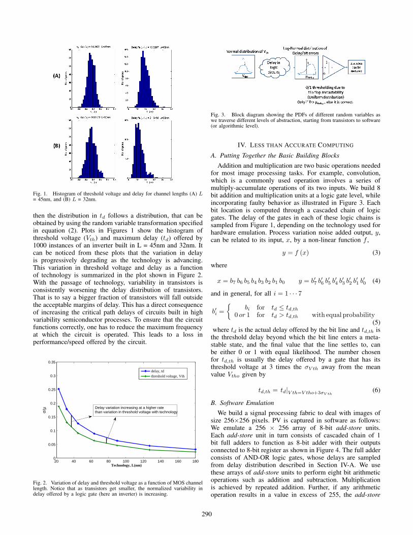
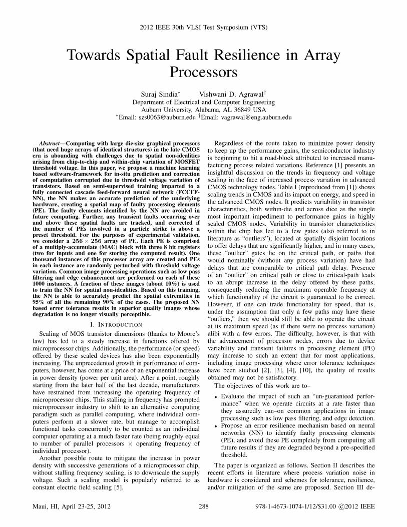
Fig. 1. Histogram of threshold voltage and delay for channel lengths (A) L= 45nm, and (B) L = 32nm.
then the distribution in td follows a distribution, that can beobtained by using the random variable transformation specifiedin equation (2). Plots in Figures 1 show the histogram ofthreshold voltage (Vth) and maximum delay (td) offered by1000 instances of an inverter built in L = 45nm and 32nm. Itcan be noticed from these plots that the variation in delayis progressively degrading as the technology is advancing.This variation in threshold voltage and delay as a functionof technology is summarized in the plot shown in Figure 2.With the passage of technology, variability in transistors isconsistently worsening the delay distribution of transistors.That is to say a bigger fraction of transistors will fall outsidethe acceptable margins of delay. This has a direct consequenceof increasing the critical path delays of circuits built in highvariability semiconductor processes. To ensure that the circuitfunctions correctly, one has to reduce the maximum frequencyat which the circuit is operated. This leads to a loss inperformance/speed offered by the circuit.
20 40 60 80 100 120 140 160 1800
0.05
0.1
0.15
0.2
0.25
0.3
0.35
Technology, L(nm)
σ/µ
delay, tdthreshold voltage, Vth
Delay variation increasing at a higher rate than variation in threshold voltage with technology
Fig. 2. Variation of delay and threshold voltage as a function of MOS channellength. Notice that as transistors get smaller, the normalized variability indelay offered by a logic gate (here an inverter) is increasing.
Fig. 3. Block diagram showing the PDFs of different random variables aswe traverse different levels of abstraction, starting from transistors to software(or algorithmic level).
IV. LESS THAN ACCURATE COMPUTING
A. Putting Together the Basic Building Blocks
Addition and multiplication are two basic operations neededfor most image processing tasks. For example, convolution,which is a commonly used operation involves a series ofmultiply-accumulate operations of its two inputs. We build 8bit addition and multiplication units at a logic gate level, whileincorporating faulty behavior as illustrated in Figure 3. Eachbit location is computed through a cascaded chain of logicgates. The delay of the gates in each of these logic chains issampled from Figure 1, depending on the technology used forhardware emulation. Process variation noise added output, y,can be related to its input, x, by a non-linear function f ,
y = f (x) (3)
where
x = b7 b6 b5 b4 b3 b2 b1 b0 y = b′7 b′6 b
′5 b
′4 b
′3 b
′2 b
′1 b
′0 (4)
and in general, for all i = 1 · · · 7
b′i =
{bi for td ≤ td,th
0 or 1 for td > td,th with equal probability(5)
where td is the actual delay offered by the bit line and td,th isthe threshold delay beyond which the bit line enters a meta-stable state, and the final value that the line settles to, canbe either 0 or 1 with equal likelihood. The number chosenfor td,th is usually the delay offered by a gate that has itsthreshold voltage at 3 times the σV th away from the meanvalue Vtho given by
td,th = td|V th=V tho+3σV th(6)
B. Software Emulation
We build a signal processing fabric to deal with images ofsize 256×256 pixels. PV is captured in software as follows:We emulate a 256 × 256 array of 8-bit add-store units.Each add-store unit in turn consists of cascaded chain of 1bit full adders to function as 8-bit adder with their outputsconnected to 8-bit register as shown in Figure 4. The full adderconsists of AND-OR logic gates, whose delays are sampledfrom delay distribution described in Section IV-A. We usethese arrays of add-store units to perform eight bit arithmeticoperations such as addition and subtraction. Multiplicationis achieved by repeated addition. Further, if any arithmeticoperation results in a value in excess of 255, the add-store
290

Fig. 4. Synthesis of 256×256 MAC array, with PV noise added for softwareemulation of PV degraded hardware.
elements are designed to saturate to 255, thus mimicking real-world scenario where 8-bit gray scale images have a maximumintensity level of 255. For simplicity, we do not use colorimages and restrict ourselves to the use of gray scale imagesin all our experiments, as we shall see in the sequel.
V. IMAGE DEGRADATION IN LOW PASS FILTERING ANDEDGE ENHANCEMENT
We conducted a low pass filter operation on two test images“cameraman” and “baby face”. For both the test images, werepeated the experiment with and without process variation.For low pass filtering, we used the mask:
ξ = .25×(
1 11 1
)(7)
From both the images that we subjected to low pass fil-tering on the processor with process variation noise added,we find that the resulting images tend to have an increasedconcentration of scattered white and black spots (similar tosalt and pepper noise). We also notice that the concentrationof white saturated points is more than black points. This can bereasoned out as follows: Low pass filtering which is averagingtends to increase the low level intensities. If there are any MSBbit flips to zero (making the value smaller than what it shouldbe), in the early portions of the processing, their effect getsalleviated over subsequent steps of filtering. However, if thereis a MSB bit flip to a 1, this effect tends to be cumulative,often giving rise to an increased concentration of bright spots.
Edge enhancement is an image processing operation wherethe spatial discontinuities in pixel values of an image arecomputed, and they are then added to the original image toemphasize these discontinuities; the resulting image is usuallya sharper-looking version of the original image. Figure 5shows edge enhanced image obtained from processing withoutand with process variation. The degree of sharpness itselfdepends on the fraction of the edge information added to theoriginal image. Notice the pronounced accumulation of whitespots in the edge enhanced image due to the cumulative effectof bits flipping to 1. For high pass (HP) filtering, which is anintermediate step to find the edges in the original image, weuse the spatial HP filter mask:
Fig. 5. Comparison of “Camera-man” and “baby-face” image withprocessing–low pass filtering with mask ξ on “Camera-man” and edgeenhancement with HP mask ψ on “baby-face”–carried out on hardware with,and without process variation. Process variation noise added is equivalent tothe model developed for 32nm technology node (delay σ/µ = 13.5%).
ψ =
(1 −1−1 1
)(8)
VI. ERROR TOLERANCE USING NEURAL NETWORK
Neural networks are known to be inherently resilient [8] tofaults in their basic computing elements–neurons. This servedas the motivation for the use of neural networks for identifyingfaulty pixels, since the hardware used for building the NN isalso assumed to have the same level of process variation asthe PE. In the following sections, we shall describe the neuralnetwork architecture used for on-line identification of faultypixel locations, data set and training of NN, and the validationphase of the proposed neural network for different levels ofprocess variation noise and different sets of input images used.
A. Neural Network ArchitectureThe neural network serves to decide the pixel locations
that are faulty across a range of different input images andlevels of process variation noise in the underlying hardware.In order to achieve such a pixel-fault identification, we use afully connected cascade feed-forward neural network (FCCFF-NN) [12]. FCCFF-NN are known to solve hard problemsuch as N−input odd parity problem with a maximum oflog2 (N + 1) neurons, while the conventional multilayer feedforward network, with one hidden layer, without cascade,requires as many as N neurons. The choice of FCCFF-NN wascritical for this application since we have a total of 8×8 = 256inputs and an architecture that is efficient in the number ofneurons will allow an area efficient hardware implementation.The neural network used is shown in Figure 6. It has 256inputs, and 256 outputs. Each input to the NN is a PE outputfrom the most recently computed operation. The outputs of theNN can take values in the range -1 through 1; with -1 implyingthe computed value by PE is very likely to be incorrect and +1if the computed value by the PE is very likely to be correct.The neurons in the hidden layer (colored blue in Figure 6) areall bipolar with hard activation function. The output neurons(colored red in Figure 6) are weighted summing blocks of thepreceding hidden neurons and the inputs. We use 36 hidden
291

Fig. 6. Fully connected cascade feed-forward neural network. Bipolarneurons with hard activation are used for hidden layer, while output neuronsare weighted summers of outputs from all the hidden neurons and inputs.
neurons connected as a fully connected cascade, in additionto the 256 output summing blocks (alternately referred to asoutput neurons in the paper). Transfer functions of both thesetype of neurons is shown in Figure 6. We will next describe thedata sets used for training and the training procedure impartedto the neural network for faulty pixel identification.
B. Content Rich Data Sets for TrainingThere are three control parameters that can be varied in
order to gather sufficiently content rich data for setting upthe NN training. First, the original input image that is to beprocessed on the PE array. Second, the underlying hardwareused for processing the images. Finally, the operation to beperformed on this image-either low pass filtering or edgeenhancement.
As for the first control parameter, we used 10 images, twoof which are shown in Figure 5. For diversity in the secondcontrol parameter, we created 1000 instances of the PE arrayshown in Figure 4. Gates in each instance of the PE arrayare assigned random delays sampled from the PDF of gatedelay distribution at the 32nm technology node (for example,delay distribution of an inverter in 32nm node is shown inFigure 1). Out of these 1000 instances, 100 instances are usedfor processing images to generate sufficient data for training.Finally, for the last control parameter, we use five of the tenimages for low pass filtering (we will refer to it as LP group),and the rest for edge enhancement (referred to as EE group).Each of the five images from LP and EE group are processedon all 100 instances of the PE array. Thus we have a totalof 100 × (5 + 5) = 1000 images for training the NN. Nextto serve as a reference (ideal output from PE array) in thetraining phase, we process each of the five images from boththe groups on a fault-free PE array resulting in 10 images.
C. Training the Neural NetworkFrom the outputs of the original PE array of size 256×256,
blocks of size 8×8 are used as input to the NN. Each output ofthe NN has a possible range of [-1,1]. The outputs of the NNare trained to take values of -1 if there is a difference beyond athreshold τ between PV degraded output and the ideal output,and are trained to take the value 1 if the difference is less than
0 200 400 600 800 100090
92
94
96
98
100
Index of PE array instance
Acc
urac
y of
det
ectio
n (A
D)
τ =50τ = 20
Fig. 7. Accuracy of detection of faulty pixels in different instances (1–900)by the neural network for a threshold τ = 20 and τ = 50.
this threshold τ . The value τ can be set any value between aminimum 1 and a maximum of 255. Setting a value of τ = 1would imply the margin for error is tight, and that any PEwhose computation leads to even one intensity level differentfrom the ideal value will be considered faulty. Conversely, ifτ is set to a higher value then PE whose computed resultsare within τ intensity levels of the ideal value are consideredfault-free.
We use neuron by neuron (NBN) training algorithm [13],which has significantly improved convergence when comparedto the conventional error back propagation training for FCCFF-NN. The NBN training kit is available online at [11].
D. Validation of Neural Network TrainingThe NN training imparted is now validated on a new data
set. This is drawn as follows: A fresh set of 10 images notused in the training phase is chosen. These are split again intoLP group and EE group. Each of the five images from both thegroups are processed on the remaining 900 instances of thePE array that was created earlier. This amounts to every arrayinstance being tested with 10 image processing operations–fivefor LP filtering and the rest for edge enhancement.
We now characterize performance of the NN with twofigures of merit: 1) accuracy of detection (AD) and 2) mis-prediction (MP ). For a given array instance, if Nact is thenumber of PE that are faulty, that is PE whose computed valueis different from the desired value by more than threshold τ(We used τ = 20 for all instances); and Ndetect is the numberof PE that was found by the NN to be faulty accurately, thenwe define, accuracy of detection (AD) to be
AD =Ndetect
Nact. (9)
We define mis-prediction (MP ) to be the ratio of numberof PE, Nmis−pred, that were found to be faulty incorrectly bythe NN to the total number of PE that are actually fault free.We therefore have
MP =Nmis−pred
Ntot −Nact, (10)
where Ntot is the total number of PE in the array. In ourexperiments, we have Ntot = 65536.
Figure 7 shows bar graph of the accuracy with whichindividual PE were identified as faulty by the NN for each
292

0 200 400 600 800 10000
1
2
3
4
5
Index of PE array instance
Mis
pred
ictio
n (M
P)
%
τ = 50τ = 20
Fig. 8. Rate of mis-prediction (in %) by NN for threshold τ = 20 andτ = 50 for all instances. The means are 0.5% and 0.3% for τ = 20 andτ = 50, respectively.
instance (plotted along the x-axis). Mean accuracy is 95%.We repeat the experiment with another value of τ = 50,and find that the performance of the NN improves to a meanaccuracy of 97%. This can be reasoned as follows: differencebetween actual and desired PE values become discernible asthe difference increases; neurons in the neural network, similarto the human eye, can perceive differences better when itis greater. Figure 8 shows a bar graph of mis-prediction fordifferent array instances by the NN. Again, higher thresholdτ = 50 results in much smaller mis-prediction. We next lookat an on-line error tolerance scheme using this trained NN.
E. On-Line Error TolerancePE identified to have been faulty by the NN is precluded
from future computation, instead re-using PE whose perfor-mance is acceptable. Such a scheme while requires additionaltime due to PE re-use, it offers significant benefits in thequality of images perceived. Figure 9 shows a test image“Lena” processed (LP filtered) on a PE array with and withoutprecluding faulty elements as predicted by NN. We see signif-icant improvement in visual quality when NN based decisionis used for excluding PE that are faulty and re-using PE’sthat are deemed to be good by NN. Further NN monitors PEoutputs after each operation, and continuously updates list ofPE that are faulty, which allows the scheme to be resilientagainst transient errors.
VII. CONCLUSION AND FUTURE WORK
A neural network based on-line error tolerance scheme forcountering process variation related degradation in array pro-cessors was proposed. The key take-away from this work is thedemonstration of spatial tolerance without having to increaseredundancy in the processing elements. Instead, we use anintermediate layer of intelligence such as neural network toidentify which computation is good enough and which is not.While neural networks can serve to identify the faulty elementsin array processors, greater investigation is required on thepossibility of using NN itself as PE [2] in the array so that onecan leverage the error resilient properties of neural network.
REFERENCES
[1] S. Borkar, “Design Perspectives on 22nm CMOS and Beyond,”in Proc. 46th ACM/IEEE Design Automation Conf., July 2009,pp. 93–94.
[2] M. A. Breuer, S. K. Gupta, and T. M. Mak, “Defect and ErrorTolerance in the Presence of Massive Numbers of Defects,”IEEE Design & Test of Computers, vol. 21, no. 3, pp. 216–227,May-June 2004.
Fig. 9. A test image “Lena” illustrating improved visual quality with achievedwith the NN based error tolerance. Notice the increased white spots in the PVdegraded image (right top) due to the accumulated effect of MSBs flipping.
[3] I. S. Chong and A. Ortega, “Hardware Testing for Error TolerantMultimedia Compression Based on Linear Transforms,” in Proc.20th IEEE Int. Symp. Defect and Fault Tolerance in VLSISystems, Oct. 2005, pp. 523–531.
[4] H. Chung and A. Ortega, “Analysis and Testing for ErrorTolerant Motion Estimation,” in Proc. 20th IEEE Int. Symp.Defect and Fault Tolerance in VLSI Systems, Oct. 2005, pp.514–522.
[5] B. Davari, R. H. Dennard, and G. G. Shahidi, “CMOS Scalingfor High Performance and Low Power - the Next Ten Years,”Proc. IEEE, vol. 83, no. 4, pp. 595–606, Apr. 1995.
[6] R. Hegde and N. R. Shanbhag, “Energy-Efficient Signal Pro-cessing via Algorithmic Noise-Tolerance,” in Proc. InternationalSymp. Low Power Electronics and Design, 1999, pp. 30–35.
[7] K. V. Palem, “Energy Aware Computing Through ProbabilisticSwitching: A Study of Limits,” IEEE Trans. Computers,, vol. 54,no. 9, pp. 1123–1137, Sept. 2005.
[8] M. N. O. Sadiku and M. Mazzara, “Computing with NeuralNetworks,” IEEE Potentials, vol. 12, no. 3, pp. 14–16, Oct. 1993.
[9] S. Sindia, F. F. Dai, V. D. Agrawal, and V. Singh, “Impact ofProcess Variations on Computers used for Image Processing,”in Proc. IEEE Int. Symp. Circuits and Systems, May 2012.
[10] G. V. Varatkar and N. R. Shanbhag, “Error-Resilient MotionEstimation Architecture,” IEEE Trans. Very Large Scale Inte-gration Systems, vol. 16, no. 10, pp. 1399–1412, Oct. 2008.
[11] B. M. Wilamowski, “Neuron by Neuron Trainer 2.0.”http://131.204.128.91/NNTrainer/index.php, accessed on Oct.10, 2011.
[12] B. M. Wilamowski, D. Hunter, and A. Malinowski, “SolvingParity-N Problems With Feedforward Neural Networks,” inProc. International Joint Conf. Neural Networks, volume 4, July2003, pp. 2546–2551.
[13] B. M. Wilamowski and H. Yu, “Neural Network Learning With-out Backpropagation,” IEEE Trans. Neural Networks, vol. 21,no. 11, pp. 1793–1803, Nov. 2010.
[14] X. Yuan, T. Shimizu, U. Mahalingam, J. S. Brown, K. Z. Habib,D. G. Tekleab, T.-C. Su, S. Satadru, C. M. Olsen, H. Lee, L.-H.Pan, T. B. Hook, J.-P. Han, J.-E. Park, M.-H. Na, and K. Rim,“Transistor Mismatch Properties in Deep-Submicrometer CMOSTechnologies,” IEEE Trans. Electron Devices, vol. 58, no. 2, pp.335–342, Feb. 2011.
293


![[Array, Array, Array, Array, Array, Array, Array, Array, Array, Array, Array, Array]](https://img.dokumen.tips/doc/110x75/56816460550346895dd63b8b/array-array-array-array-array-array-array-array-array-array-array.jpg)