Embed Size (px)
Citation preview
© Fraunhofer
Towards Roll-to-Roll Fabrication of Electronic Functions on Plastic Films
Gerhard Klink Fraunhofer Research Institution for Modular Solid State Technologies Hansastraße 27d, 80686 München
© Fraunhofer
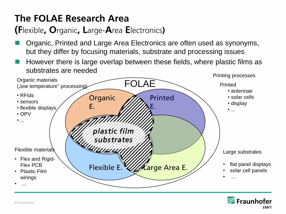
The FOLAE Research Area (Flexible, Organic, Large-Area Electronics)
Organic, Printed and Large Area Electronics are often used as synonyms,
but they differ by focusing materials, substrate and processing issues
However there is large overlap between these fields, where plastic films as
substrates are needed
Organic materials
(„low temperature“ processing)
• RFIds
• sensors
• flexible displays
• OPV
• ...
Large substrates
• flat panel displays
• solar cell panels
• ...
Printing processes
Printed
• antennae
• solar cells
• display
• ...
FOLAE
Flexible materials
• Flex and Rigid-
Flex PCB
• Plastic Film
wirings
• ...
Organic E.
Printed E.
plastic film substrates
Large Area E. Flexible E.

© Fraunhofer
Large-Area Electronics
Flat panel displays
Solar panels
Wiring systems
rigid substrates flexible substrates
Large-Volume Devices
Antennas and RFID
EL Lamp
Single-use sensors
© Fraunhofer
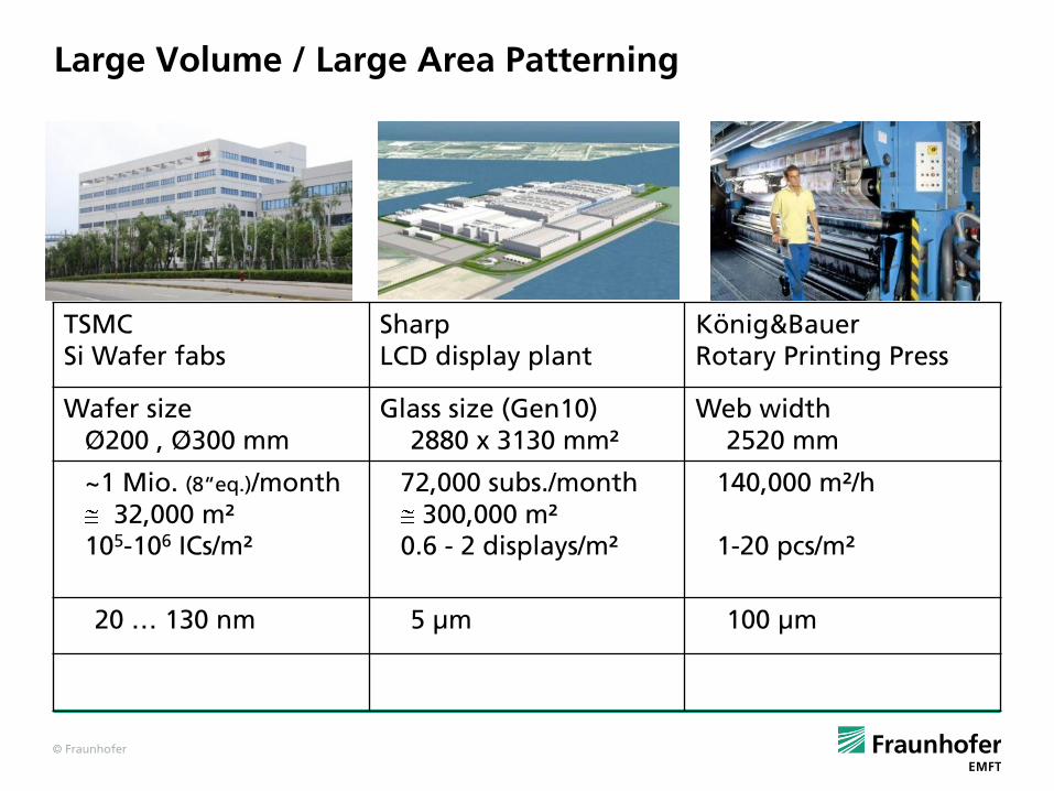
Large Volume / Large Area Patterning
TSMC Si Wafer fabs
Sharp LCD display plant
König&Bauer Rotary Printing Press
Wafer size Ø200 , Ø300 mm
Glass size (Gen10) 2880 x 3130 mm²
Web width 2520 mm
~1 Mio. (8“eq.)/month 32,000 m² 105-106 ICs/m²
72,000 subs./month 300,000 m² 0.6 - 2 displays/m²
140,000 m²/h 1-20 pcs/m²
20 … 130 nm 5 µm 100 µm
© Fraunhofer
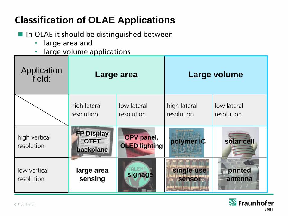
Classification of OLAE Applications
Application field:
Large area Large volume
high lateral
resolution
low lateral
resolution
high lateral
resolution
low lateral
resolution
high vertical
resolution
FP Display
OTFT
backplane
OPV panel,
OLED lighting polymer IC solar cell
low vertical
resolution
large area
sensing signage
single-use
sensor
printed
antenna
In OLAE it should be distinguished between • large area and • large volume applications
© Fraunhofer
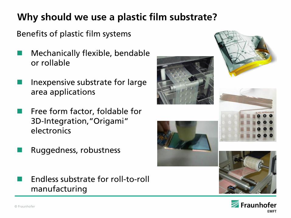
Why should we use a plastic film substrate?
Benefits of plastic film systems
Mechanically flexible, bendable or rollable
Inexpensive substrate for large area applications
Free form factor, foldable for 3D-Integration,“Origami“ electronics
Ruggedness, robustness
Endless substrate for roll-to-roll manufacturing
© Fraunhofer
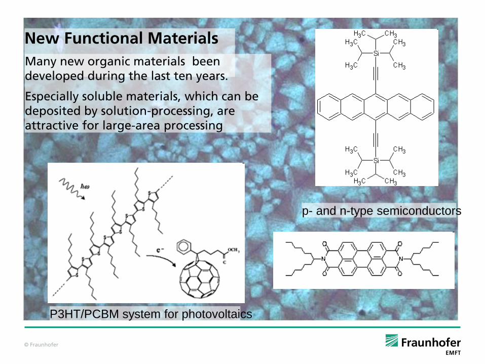
New Functional Materials
Many new organic materials been developed during the last ten years.
Especially soluble materials, which can be deposited by solution-processing, are attractive for large-area processing
P3HT/PCBM system for photovoltaics
p- and n-type semiconductors

© Fraunhofer
other functional materials
electronic devices photonic devices
OLED
OPV
oTFT
peripherials
Sensor
Display
Lighting Solar Cell
rollable line driver
active matrix backplane
ID circuits
flexible and rollable display
RF interface
RFId
organic semiconductor
battery
Memory
Family Tree of Organic Electronics
© Fraunhofer
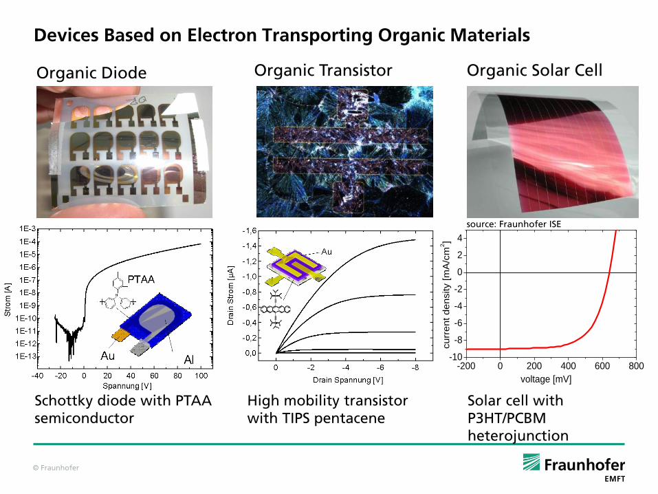
Devices Based on Electron Transporting Organic Materials
© Fraunhofer IZM
Organic Diode
source: Fraunhofer ISE
-200 0 200 400 600 800-10
-8
-6
-4
-2
0
2
4
curr
ent de
nsity [m
A/c
m2]
voltage [mV]
Organic Transistor Organic Solar Cell
Schottky diode with PTAA semiconductor
High mobility transistor with TIPS pentacene
Solar cell with P3HT/PCBM heterojunction

© Fraunhofer
Amorphous Semiconductor
PTAA
Architecture
Top-Gate / Bottom Contact
Status:
• p-type oTFTs
• On/off ratio 1000
Disadvantage:
• low mobility (10-3)
• high threshold 10 – 15 V
• low on-current (10-9 A/sq.)
• yield problems („hard yield“)
• instable above 100
C in air
Schema:
20
10-8
10-7
10-6
10-5
-50 -40 -30 -20 -10 0 10
Gate-Voltage Vg [V]
Cu
rre
nt I
d [A
]
10-9
Vds=-50 V
l= 20 µm
w/l= 2000
PTAA Transferkennlinie
© Fraunhofer
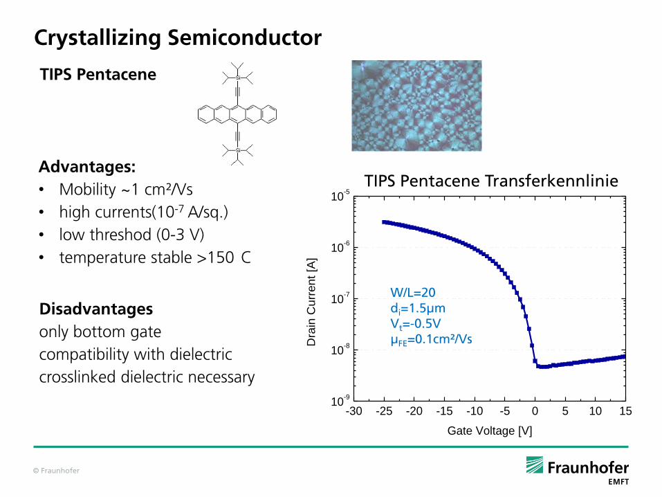
Crystallizing Semiconductor
W/L=20 di=1.5µm Vt=-0.5V µFE=0.1cm²/Vs
TIPS Pentacene
Advantages:
• Mobility ~1 cm²/Vs
• high currents(10-7 A/sq.)
• low threshod (0-3 V)
• temperature stable >150
C
Disadvantages
only bottom gate
compatibility with dielectric
crosslinked dielectric necessary
TIPS Pentacene Transferkennlinie
-30 -25 -20 -15 -10 -5 0 5 10 1510
-9
10-8
10-7
10-6
10-5
Dra
in C
urr
ent
[A]
Gate Voltage [V]
© Fraunhofer
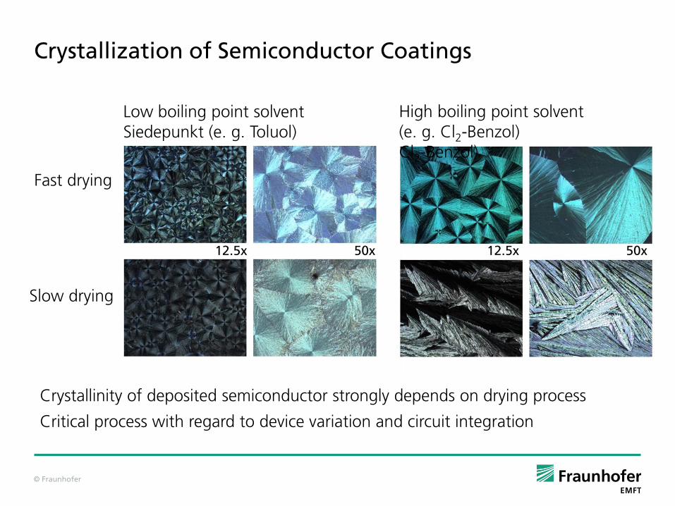
Crystallization of Semiconductor Coatings
Low boiling point solvent Siedepunkt (e. g. Toluol)
Fast drying
12.5x 50x 12.5x 50x
High boiling point solvent (e. g. Cl2-Benzol) Cl2-Benzol)
Slow drying
Crystallinity of deposited semiconductor strongly depends on drying process
Critical process with regard to device variation and circuit integration
© Fraunhofer
Circuit schematics
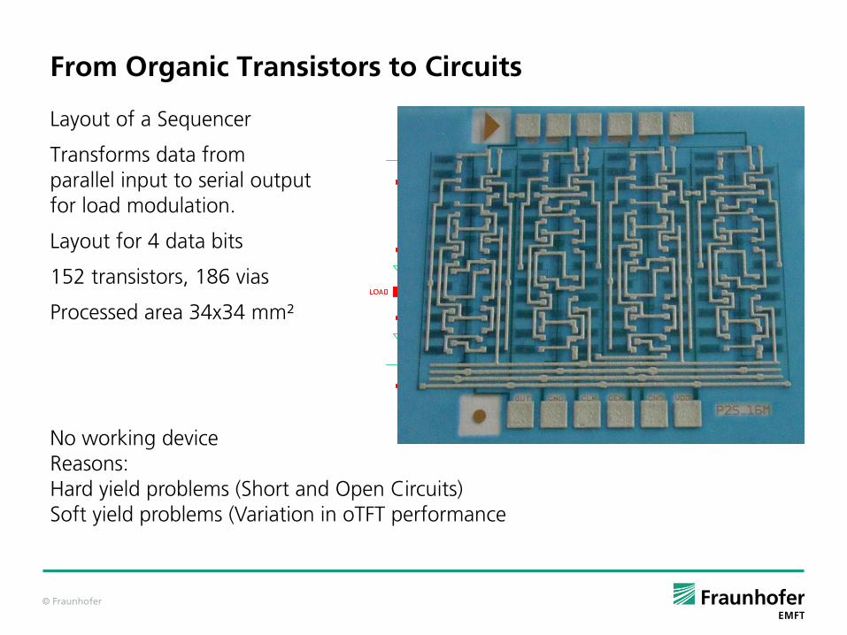
From Organic Transistors to Circuits
Layout of a Sequencer
Transforms data from parallel input to serial output for load modulation.
Layout for 4 data bits
152 transistors, 186 vias
Processed area 34x34 mm²
No working device Reasons: Hard yield problems (Short and Open Circuits) Soft yield problems (Variation in oTFT performance
© Fraunhofer
1,0E-14
1,0E-13
1,0E-12
1,0E-11
1,0E-10
1,0E-09
1,0E-08
0 200 400 600 800
d [nm]
I_le
ak [A
/mm
^2]
batch 03
batch 04
slot die 1
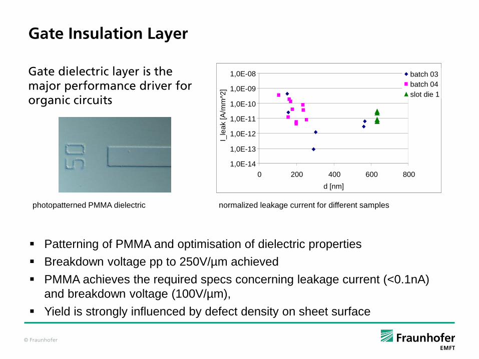
Patterning of PMMA and optimisation of dielectric properties
Breakdown voltage pp to 250V/µm achieved
PMMA achieves the required specs concerning leakage current (<0.1nA)
and breakdown voltage (100V/µm),
Yield is strongly influenced by defect density on sheet surface
normalized leakage current for different samples
Gate Insulation Layer Gate dielectric layer is the major performance driver for organic circuits
photopatterned PMMA dielectric
© Fraunhofer
0
10
20
30
40
50
0 10 20 30 40 50 Vin / [V]
Vo
ut /
[V
]
Vout
Vin
0
10
20
30
40
50
0 10 20 30 40 50
Vin / Vout [V]
Vo
ut /
Vin
[V]
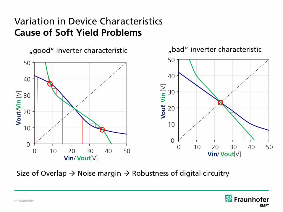
Variation in Device Characteristics Cause of Soft Yield Problems
„good“ inverter characteristic
Size of Overlap Noise margin Robustness of digital circuitry
„bad“ inverter characteristic

© Fraunhofer
Ring Oscillators (p-type)
Amplification nearly 1
Noise margin is much too low to get oscillation
Vo
ut
/ V
in [
V]
0
5
10
15
20
25
30
0 5 10 15 20 25 30 Vin / Vout [V]
Individual inverter Averaged charact.l Mirrored Vin/Vout

© Fraunhofer
Complementary oTFTs – Organic “CMOS”
Higher definition of switching levels makes complementary logic circuits more robust against variation in characteristics
Switched state is always high resistance, low power consumption
But! More complicated processing (deposition of two semiconductor materials)
switch
load
Vs
Vout
Vin
S
D
G
S
D
G
0 V
Vs
n-channel
p-channel
Vout Vin
S
D
G
S
D
G
Vss
Vdd
Vin
Vout
Vs
Vs
ViH ViL
VoL
VoH
Vin
Vout
Vs
Vs
ViH ViL
VoL
VoH
Inverter in PMOS technology Inverter in CMOS technology

© Fraunhofer
Organic n-type Semiconductor
N1500 n-type (C) n-type (Au)
VT (V) ~ -4 undefined
µsat (cm2/Vs)
0,07 undefined
µp/µn 0,29
Ion ~10µA <100 nA
Ioff ~400 nA ~ 10 nA Ion/Ioff 25 <10
N3000 n-type (Au)
OSC1
Ion 100 nA – 3 µA
Ioff 0.5 – 50 nA
Ion/Ioff 500 - 2000 large variablity (dev2dev)
Proprietary materials from Polyera Corp. (based on Perylene)

© Fraunhofer
Alignment in Plastic Film Processing
Stop&Go Roll-to-Roll Distance defined by web transport
gk
Distance defined by lithography tool
e. g. print cylinder
Continuous Roll-to-Roll

© Fraunhofer
Processing Flexible Electronics – From Single Substrates to Continuous Printing
single substrates or
carriers
stop&go from roll to
roll
“true” rotational
printing
electronic packaging flex technologies graphic arts printing
single sheets 1 – 3 m/min 100 m/min and more
high precision and
resolution
precision combined with
easier handling
high throughput
electronic defect free
(pass or fail)
defect free, but
compromises
visible defect free
(gradual steps)
traditional electronics cost-efficient electronics ubiquitous electronics
single item tagging
volume
cost

© Fraunhofer
Reel-to-Reel Lab at Fraunhofer EMFT
Fine-line patterning of metallized plastic films Thick-film screen printing on sheets and rolls
Electrical testing Laser processing Foil lamination Sputter deposition Web coating
© Fraunhofer
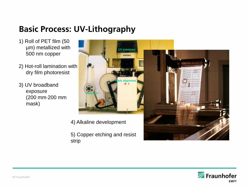
Basic Process: UV-Lithography
1) Roll of PET film (50
µm) metallized with
500 nm copper
2) Hot-roll lamination with
dry film photoresist
3) UV broadband
exposure
(200 mm·200 mm
mask)
mask alignment
UV exposure
spooler
despooler
4) Alkaline development
5) Copper etching and resist
strip

© Fraunhofer
Reel-to-Reel Application Center - Equipment Screen printer with belt oven and UV curing (Aurel S. A.)
unwinder printer buffer UV cure oven (4 zones) spooler
© Fraunhofer
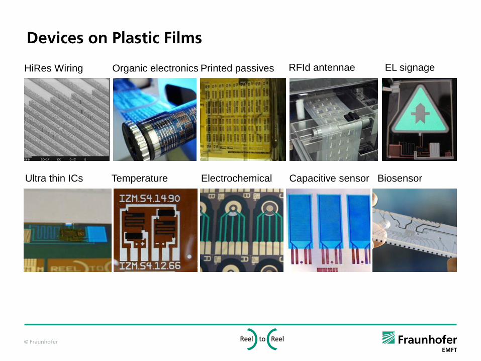
Devices on Plastic Films
RFId antennae Organic electronics EL signage HiRes Wiring Printed passives
Temperature Electrochemical Ultra thin ICs Capacitive sensor Biosensor

© Fraunhofer
Technological Challenges for Processing on Plastic Films
Non-planar substrate needs support or tensile stress
Tensile stress leads to stretching
Uptake of water and other vapours during processing
Dimensional changes due to heat, water, solvent
Contaminated surface (particles, chemicals)
Impact of film stresses (wrinkling)
© Fraunhofer
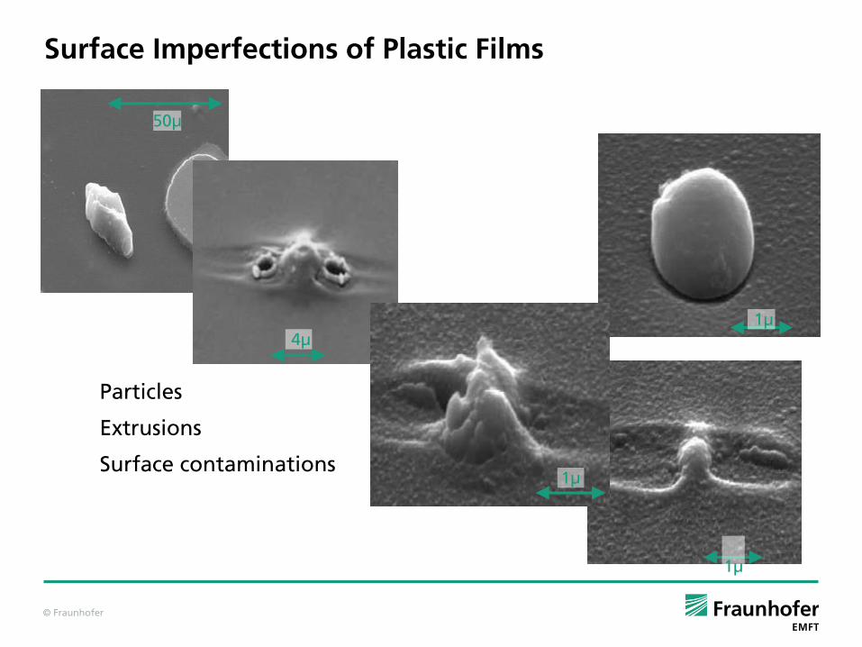
Surface Imperfections of Plastic Films
Particles
Extrusions
Surface contaminations
50µ
1µ 4µ
1µ
1µ

© Fraunhofer
Uptake of Water, Other Gases and Vapours
Plastic films are not as compact as rigid substrates. Gases and also chemicals penetrate them and can be absorbed.
Common problem for plastic films is water uptake
1,0E-08
1,0E-07
1,0E-06
1,0E-05
1,0E-04
1,0E-03
7:00 9:00 11:00 13:00 15:00 17:00 19:00 21:00
time
p [
mb
ar]
chamber ws
chamber dc2
Outgassing of plastic film in R2R vacuum equipment

© Fraunhofer
Dimensional Changes Caused by Heat and Web Tension
There is a predictable part (reproducable), which can be corrected, and
Random part, which can not be corrected and determines alignment accuracy
Melinex 501
-1.0%
-0.5%
0.0%
0.5%
change in machine direction
chan
ge i
n t
ran
svers
e d
irect
ion
250 N/m 100 N/m
0 N/m
-1.0% -0.5% 0.0% 0.5%
100
C
120
C
150
C
82 mm

© Fraunhofer
Cracking of Thin Layers
Plastic films are stretchable
Higher thermal expansion than anorganic materials
May result in cracking of thin films during deposition or further processing
Depends on brittleness, plasticity and thickness
Cracked chromium metallisation sputtered on PEN
200 µ
© Fraunhofer
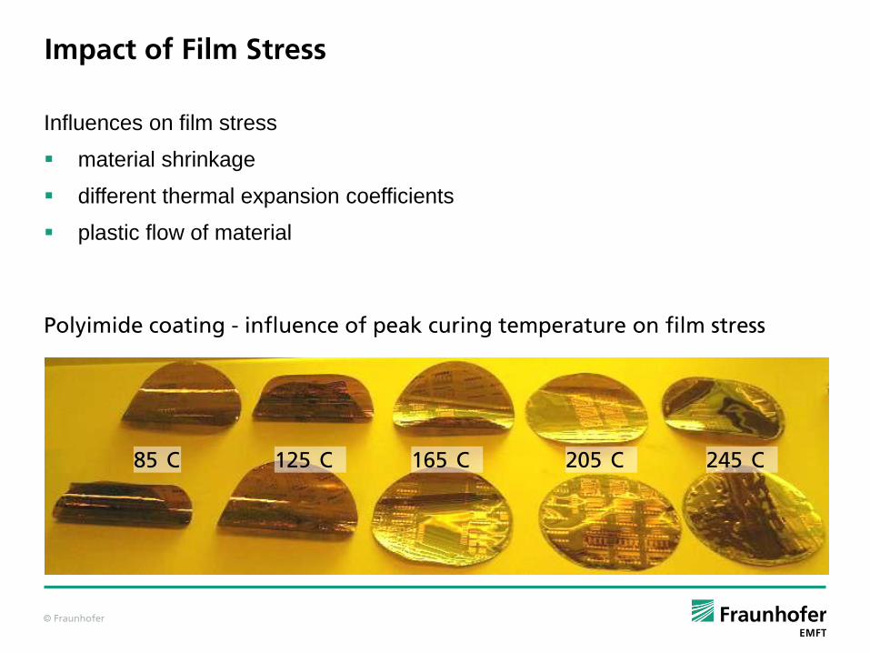
Impact of Film Stress
85
C 125
C 165
C 205
C 245
C
Polyimide coating - influence of peak curing temperature on film stress
Influences on film stress
material shrinkage
different thermal expansion coefficients
plastic flow of material

© Fraunhofer
Multilayer Wiring on Plastic Films
Basis for system integration is a
wiring of at least two conductive
layers:
Layer 1:
High-resolution layer in thin-film
technology
Layer2:
Layer 1:
Electroplated
copper
Printed 2nd wiring (Ag
paste)
electroplated 2nd
wiring (Ag paste)
Low-cost version with printed conductors
High wiring density with thin-film conductors

© Fraunhofer
Fabrication of Vias - Laser Drilled Holes in Plastic Film
Holes through 50 µm polyimide
High aspect ratio vias
© Fraunhofer
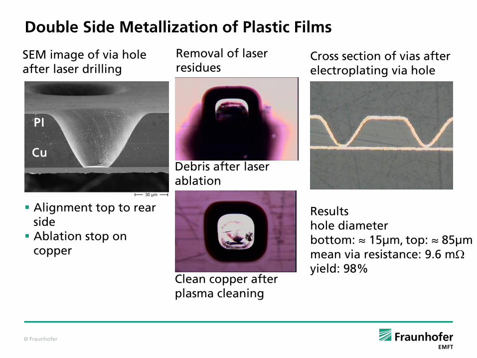
Double Side Metallization of Plastic Films
Cross section of vias after electroplating via hole
SEM image of via hole after laser drilling
PI
Cu
Removal of laser residues
Alignment top to rear side
Ablation stop on copper
Debris after laser ablation
Clean copper after plasma cleaning
Results hole diameter bottom: ≈ 15µm, top: ≈ 85µm mean via resistance: 9.6 m yield: 98%
© Fraunhofer
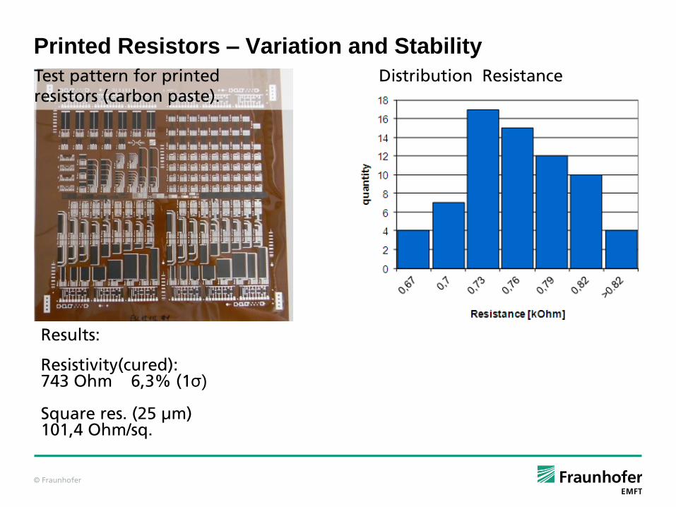
Printed Resistors – Variation and Stability
Test pattern for printed resistors (carbon paste).
Resistivity(cured): 743 Ohm
6,3% (1σ) Square res. (25 µm) 101,4 Ohm/sq.
Distribution Resistance
Results:
© Fraunhofer
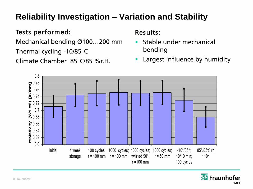
Reliability Investigation – Variation and Stability
Results :
Stable under mechanical bending
Largest influence by humidity
Tests performed:
Mechanical bending Ø100…200 mm
Thermal cycling -10/85
C
Climate Chamber 85
C/85 %r.H.
© Fraunhofer
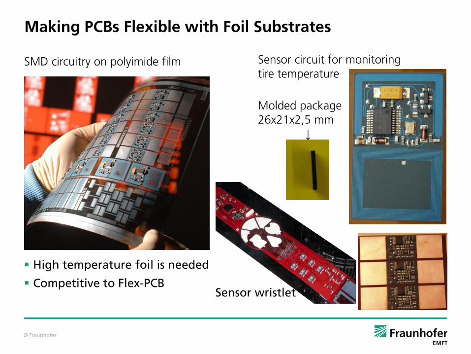
Making PCBs Flexible with Foil Substrates
SMD circuitry on polyimide film Sensor circuit for monitoring tire temperature
Molded package 26x21x2,5 mm ↓
High temperature foil is needed
Competitive to Flex-PCB Sensor wristlet
© Fraunhofer
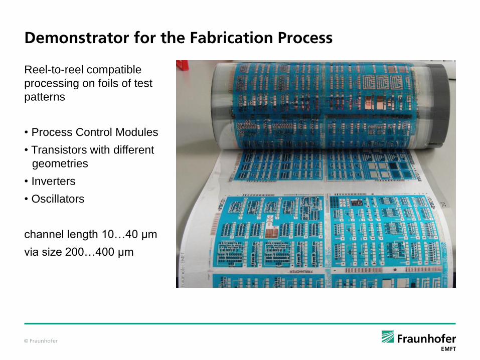
Demonstrator for the Fabrication Process
Reel-to-reel compatible
processing on foils of test
patterns
• Process Control Modules
• Transistors with different
geometries
• Inverters
• Oscillators
channel length 10…40 µm
via size 200…400 µm

38 18/07/2013 Copyright © 2010-2013 POLARIC Consortium
1,0E-14
1,0E-13
1,0E-12
1,0E-11
1,0E-10
1,0E-09
1,0E-08
0 200 400 600 800
d [nm]
I_le
ak [A
/mm
^2]
batch 03
batch 04
slot die 1
Patterning of PMMA and optimisation of dielectric properties
Breakdown voltage pp to 250V/µm achieved
PMMA achieves the required specs concerning leakage current (<0.1nA)
and breakdown voltage (100V/µm),
Yield is strongly influenced by defect density on sheet surface
normalized leakage current for different samples
Gate Insulation Layer
© Fraunhofer
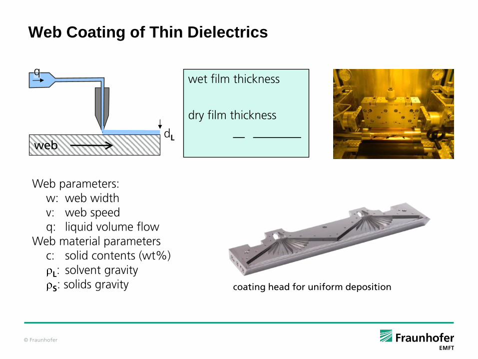
Web Coating of Thin Dielectrics
web
Web parameters: w: web width v: web speed q: liquid volume flow Web material parameters c: solid contents (wt%) L: solvent gravity S: solids gravity
wet film thickness
dry film thickness
coating head for uniform deposition
q
dL

© Fraunhofer
Roll-to-Roll Wet Coating
Doctor blade
Slot die
400
450
500
550
600
650
700
-10 -5 0 5 10
thic
kn
es
s [
nm
]
position TD [cm]
© Fraunhofer
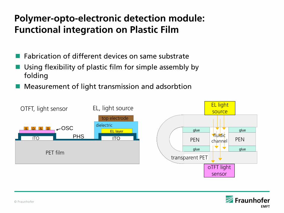
Polymer-opto-electronic detection module: Functional integration on Plastic Film
Fabrication of different devices on same substrate
Using flexibility of plastic film for simple assembly by folding
Measurement of light transmission and adsorbtion
ITO ITO
S D S D
barrier layers
EL layer
dielectric
ITO ITO
S D S D
PHS
PET film
OTFT, light sensor EL, light source
EL layer
top electrode
dielectric OSC
PEN foil
glue
glue
PEN foil
glue
glue
glue
glue
glue
glue
EL light source
fluidic channel
transparent PET
oTFT light sensor
PEN PEN

© Fraunhofer
Fluid analysis by opto-electronic absorbance measurement
Polymer-opto-electronic detection module
3000 3500 4000 4500 5000 5500 6000-3,5x10
-6
-3,0x10⁻⁶
-2,5x10⁻⁶
I dra
in (
A)
Time (s)
Rho
c1
Rho
c2Rho
c3
Rho
c4
EL
off
3000 3500 4000 4500 5000 5500 6000-3,5x10
-6
-3,0x10⁻⁶
-2,5x10⁻⁶
I dra
in (
A)
Time (s)
Rho
c1
Rho
c2Rho
c3
Rho
c4
EL
off
Rhodamine B Concentrations: c1: 0,15 mM c2: 0,46 mM c3: 1,1 mM c4: 5,5 mM
Demo device
Device parts
© Fraunhofer
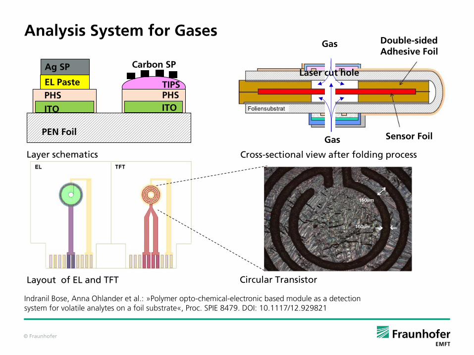
Sensor Foil
Double-sided Adhesive Foil OTFT
EL Element
Analysis System for Gases
PEN Foil
ITO
PHS
EL Paste
Ag SP
ITO
PHS TIPS
Carbon SP
Layer schematics
Laser cut hole
Gas
Gas
Layout of EL and TFT
Cross-sectional view after folding process
Circular Transistor
Indranil Bose, Anna Ohlander et al.: »Polymer opto-chemical-electronic based module as a detection system for volatile analytes on a foil substrate«, Proc. SPIE 8479. DOI: 10.1117/12.929821
© Fraunhofer
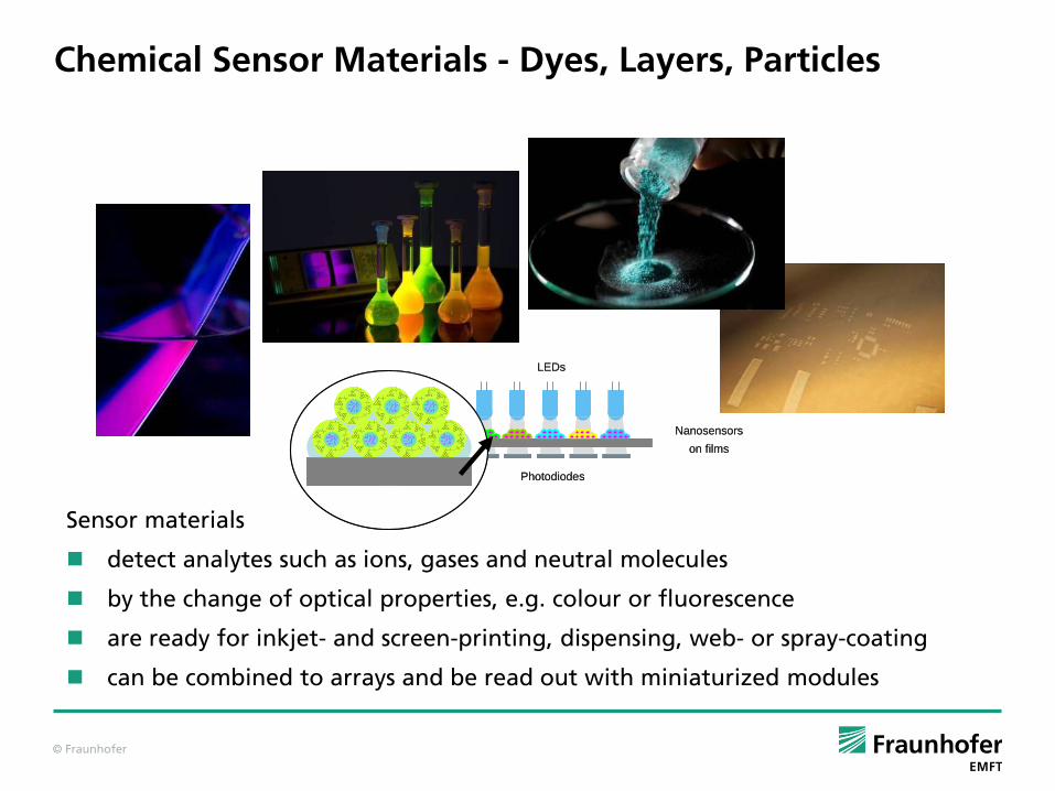
Chemical Sensor Materials - Dyes, Layers, Particles
LEDs
Photodiodes
Nanosensors
on films
O
NH
S
NH
Si
OOH
COOH
O
O
O
O
NH
S
NH
Si
OOH
COOH
O
O
O
O
NH
S
NH
Si
OOH
COOH
O
O
O
O
NH
S NH
Si
O
OH
COOH
O
O
O
O
NH
S
NH
Si
O
OH
HOOC
OO
O
O
NH
SNH
Si
O
OH
HOOC
O
O
O
O
NH
S
NH
Si
OOH
COOH
O
O
O
O
NH
S
NH
Si
OOH
COOH
O
O
O
O
NH
S
NH
Si
OOH
COOH
O
O
O
O
NH
S NH
Si
O
OH
COOH
O
O
O
O
NH
S
NH
Si
O
OH
HOOC
OO
O
O
NH
SNH
Si
O
OH
HOOC
O
O
O
O
NH
S
NH
Si
OOH
COOH
O
O
O
O
NH
S
NH
Si
OOH
COOH
O
O
O
O
NH
S
NH
Si
OOH
COOH
O
O
O
O
NH
S NH
Si
O
OH
COOH
O
O
O
O
NH
S
NH
Si
O
OH
HOOC
OO
O
O
NH
SNH
Si
O
OH
HOOC
O
O
O
O
NH
S
NH
Si
OOH
COOH
O
O
O
O
NH
S
NH
Si
OOH
COOH
O
O
O
O
NH
S
NH
Si
OOH
COOH
O
O
O
O
NH
S NH
Si
O
OH
COOH
O
O
O
O
NH
S
NH
Si
O
OH
HOOC
OO
O
O
NH
SNH
Si
O
OH
HOOC
O
O
O
O
NH
S
NH
Si
OOH
COOH
O
O
O
O
NH
S
NH
Si
OOH
COOH
O
O
O
O
NH
S
NH
Si
OOH
COOH
O
O
O
O
NH
S NH
Si
O
OH
COOH
O
O
O
O
NH
S
NH
Si
O
OH
HOOC
OO
O
O
NH
SNH
Si
O
OH
HOOC
O
O
O
O
NH
S
NH
Si
OOH
COOH
O
O
O
O
NH
S
NH
Si
OOH
COOH
O
O
O
O
NH
S
NH
Si
OOH
COOH
O
O
O
O
NH
S NH
Si
O
OH
COOH
O
O
O
O
NH
S
NH
Si
O
OH
HOOC
OO
O
O
NH
SNH
Si
O
OH
HOOC
O
O
O
O
NH
S
NH
Si
OOH
COOH
O
O
O
O
NH
S
NH
Si
OOH
COOH
O
O
O
O
NH
S
NH
Si
OOH
COOH
O
O
O
O
NH
S NH
Si
O
OH
COOH
O
O
O
O
NH
S
NH
Si
O
OH
HOOC
OO
O
O
NH
SNH
Si
O
OH
HOOC
O
O
O
O
NH
S
NH
Si
OOH
COOH
O
O
O
O
NH
S
NH
Si
OOH
COOH
O
O
O
O
NH
S
NH
Si
OOH
COOH
O
O
O
O
NH
S NH
Si
O
OH
COOH
O
O
O
O
NH
S
NH
Si
O
OH
HOOC
OO
O
O
NH
SNH
Si
O
OH
HOOC
O
O
O
O
NH
S
NH
Si
OOH
COOH
O
O
O
O
NH
S
NH
Si
OOH
COOH
O
O
O
O
NH
S
NH
Si
OOH
COOH
O
O
O
O
NH
S NH
Si
O
OH
COOH
O
O
O
O
NH
S
NH
Si
O
OH
HOOC
OO
O
O
NH
SNH
Si
O
OH
HOOC
O
O
O
O
NH
S
NH
Si
OOH
COOH
O
O
O
O
NH
S
NH
Si
OOH
COOH
O
O
O
O
NH
S
NH
Si
OOH
COOH
O
O
O
O
NH
S NH
Si
O
OH
COOH
O
O
O
O
NH
S
NH
Si
O
OH
HOOC
OO
O
O
NH
SNH
Si
O
OH
HOOC
O
O
O
O
NH
S
NH
Si
OOH
COOH
O
O
O
O
NH
S
NH
Si
OOH
COOH
O
O
O
O
NH
S
NH
Si
OOH
COOH
O
O
O
O
NH
S NH
Si
O
OH
COOH
O
O
O
O
NH
S
NH
Si
O
OH
HOOC
OO
O
O
NH
SNH
Si
O
OH
HOOC
O
O
O
O
NH
S
NH
Si
OOH
COOH
O
O
O
O
NH
S
NH
Si
OOH
COOH
O
O
O
O
NH
S
NH
Si
OOH
COOH
O
O
O
O
NH
S NH
Si
O
OH
COOH
O
O
O
O
NH
S
NH
Si
O
OH
HOOC
OO
O
O
NH
SNH
Si
O
OH
HOOC
O
O
O
O
NH
S
NH
Si
OOH
COOH
O
O
O
O
NH
S
NH
Si
OOH
COOH
O
O
O
O
NH
S
NH
Si
OOH
COOH
O
O
O
O
NH
S NH
Si
O
OH
COOH
O
O
O
O
NH
S
NH
Si
O
OH
HOOC
OO
O
O
NH
SNH
Si
O
OH
HOOC
O
O
O
O
NH
S
NH
Si
OOH
COOH
O
O
O
O
NH
S
NH
Si
OOH
COOH
O
O
O
O
NH
S
NH
Si
OOH
COOH
O
O
O
O
NH
S NH
Si
O
OH
COOH
O
O
O
O
NH
S
NH
Si
O
OH
HOOC
OO
O
O
NH
SNH
Si
O
OH
HOOC
O
O
O
O
NH
S
NH
Si
OOH
COOH
O
O
O
O
NH
S
NH
Si
OOH
COOH
O
O
O
O
NH
S
NH
Si
OOH
COOH
O
O
O
O
NH
S NH
Si
O
OH
COOH
O
O
O
O
NH
S
NH
Si
O
OH
HOOC
OO
O
O
NH
SNH
Si
O
OH
HOOC
O
O
O
O
NH
S
NH
Si
OOH
COOH
O
O
O
O
NH
S
NH
Si
OOH
COOH
O
O
O
O
NH
S
NH
Si
OOH
COOH
O
O
O
O
NH
S NH
Si
O
OH
COOH
O
O
O
O
NH
S
NH
Si
O
OH
HOOC
OO
O
O
NH
SNH
Si
O
OH
HOOC
O
O
O
O
NH
S
NH
Si
OOH
COOH
O
O
O
O
NH
S
NH
Si
OOH
COOH
O
O
O
O
NH
S
NH
Si
OOH
COOH
O
O
O
O
NH
S NH
Si
O
OH
COOH
O
O
O
O
NH
S
NH
Si
O
OH
HOOC
OO
O
O
NH
SNH
Si
O
OH
HOOC
O
O
O
O
NH
S
NH
Si
OOH
COOH
O
O
O
O
NH
S
NH
Si
OOH
COOH
O
O
O
O
NH
S
NH
Si
OOH
COOH
O
O
O
O
NH
S NH
Si
O
OH
COOH
O
O
O
O
NH
S
NH
Si
O
OH
HOOC
OO
O
O
NH
SNH
Si
O
OH
HOOC
O
O
O
O
NH
S
NH
Si
OOH
COOH
O
O
O
O
NH
S
NH
Si
OOH
COOH
O
O
O
O
NH
S
NH
Si
OOH
COOH
O
O
O
O
NH
S NH
Si
O
OH
COOH
O
O
O
O
NH
S
NH
Si
O
OH
HOOC
OO
O
O
NH
SNH
Si
O
OH
HOOC
O
O
O
O
NH
S
NH
Si
OOH
COOH
O
O
O
O
NH
S
NH
Si
OOH
COOH
O
O
O
O
NH
S
NH
Si
OOH
COOH
O
O
O
O
NH
S NH
Si
O
OH
COOH
O
O
O
O
NH
S
NH
Si
O
OH
HOOC
OO
O
O
NH
SNH
Si
O
OH
HOOC
O
O
O
O
NH
S
NH
Si
OOH
COOH
O
O
O
O
NH
S
NH
Si
OOH
COOH
O
O
O
O
NH
S
NH
Si
OOH
COOH
O
O
O
O
NH
S NH
Si
O
OH
COOH
O
O
O
O
NH
S
NH
Si
O
OH
HOOC
OO
O
O
NH
SNH
Si
O
OH
HOOC
O
O
O
Sensor materials
detect analytes such as ions, gases and neutral molecules
by the change of optical properties, e.g. colour or fluorescence
are ready for inkjet- and screen-printing, dispensing, web- or spray-coating
can be combined to arrays and be read out with miniaturized modules

© Fraunhofer
Device characterization / results
The dynamic response of the sensor with screen-printed carbon source-drain to different pH levels.
pH 4
pH 5
pH 6 pH 7
© Fraunhofer
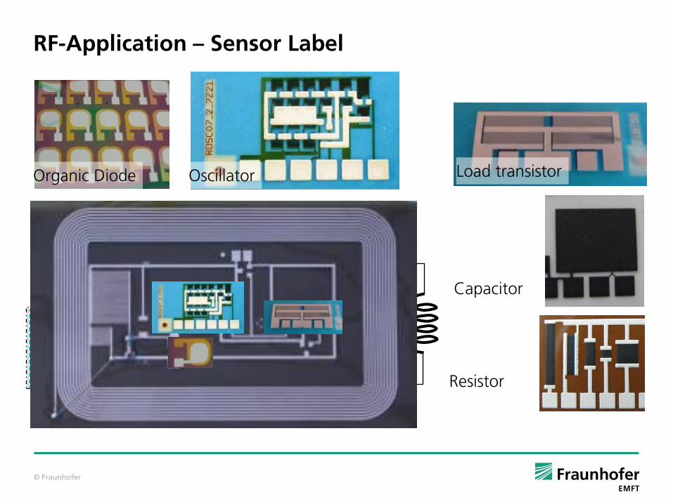
ROSC ROSC
Vload DRV
SENS
13.56 MHz
DIODE
CAP
RF-Application – Sensor Label
Organic Diode Oscillator Load transistor
Capacitor
Resistor
© Fraunhofer
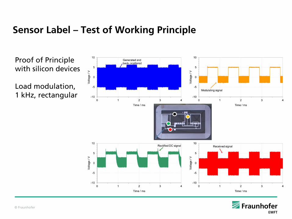
Sensor Label – Test of Working Principle
Proof of Principle with silicon devices Load modulation, 1 kHz, rectangular

© Fraunhofer
Final Remarks
A bunch of coating and patterning processes are already ready for
roll-to-roll processing
Roll-to-roll offers a better cost structure than single substrate
handling
Monolithic foil systems are still far away, system integration is needed
for electronics on plastic films
Techniques for foil processing have to be further developed,
regarding
- low temperature
- mechanical flexibility
- low thickness
- robustness and reliability

© Fraunhofer
Acknowledgements:
I thank my colleagues from the Polytronic Systems department, especially
• Dieter Bollmann
• Indranil R. Bose
• Dieter Hemmetzberger
• Anna Ohlander
• Sabine Trupp
• Prof. Karlheinz Bock
for their support to this presentation
The work presented here has been financially supported by projects granted by
German BMBF: PolyOpto (FKZ 16SV3870) European Commision:
COSMIC (GA 247681), Polaric (GA 247978) and InterFlex (GA 247710)