Embed Size (px)
DESCRIPTION
Toward Carbon Based Electronics. Philip Kim Department of Physics Columbia University. Material Platform: Low dimensional graphitic systems. 1-D: Carbon Nanotubes (since 1991) 2-D: Graphene (since 2004). Device Concepts. Conventional: (extended) CMOS, SET. Non-Conventional: - PowerPoint PPT Presentation
Citation preview

Philip Kim
Department of PhysicsColumbia University
Toward Carbon Based Electronics

Outline: Carbon Based Electronics
Material Platform: Low dimensional graphitic systems
• 1-D: Carbon Nanotubes (since 1991)• 2-D: Graphene (since 2004)
Device Concepts
Conventional: (extended) CMOS, SET
Non-Conventional: Quantum Interference, Spintronics, valleytronics

SP2 Carbon: 0-Dimension to 3-Dimension
Fullerenes (C60) Carbon Nanotubes
Atomic orbital sp2
GraphiteGraphene
0D 1D 2D 3D

Graphene : Dirac Particles in 2-dimension
Band structure of graphene (Wallace 1947)
kx
ky
Ene
rgy
kx' ky'
E
kvE F
Zero effective mass particles moving with a constant speed vF
hole
electron

Single Wall Carbon Nanotube
ky
kxkx
ky
Allowed statesMetallic nanotube
E
k1D
E
k1D
Semiconducting nanotube
Eg ~ 0.8 ev / d (nm)

400
200
0
6040200
Length (m)
Res
ista
nce
(k
)
T = 250 K
= 8 k/m
Extremely Long Mean Free Path in Nanotubes
Multi-terminal Device with Pd contact
* Scaling behavior of resistance:R(L)
5
678
10
2
3
4
5
678
100
2
3
4
5
67
0.12 4 6 8
12 4 6 8
102 4 6 8
L (m)
R (
k)
T = 250 K400
200
0
6040200
R (
k)
L (m)
R ~ RQ
R ~ L
el
L
Ne
h
Ne
hLR
22)(
le ~ 1 m
M. Purewall, B. Hong, A. Ravi, B. Chnadra, J. Hone and P. Kim, PRL (2007)Room temperature mean free path > 0.5 m

Nanotube FET
Band gap: 0.5 – 1 eVOn-off ratio: ~ 106
Mobility: ~ 100,000 cm2/Vsec @RTBallistic @RT ~ 300-500 nmFermi velocity: 106 m/secMax current density > 109 A/cm2
Vsd (V)0-0.4-0.8-1.2
I sd (A
)
Ph. Avouris et al, Nature Nanotechnology 2, 605 (2007)
Schottky barrier switching

Advantages of CNTFET
• Novel architecture ->Band-to-band tunneling FET:
subthreshold slop ~ 40 meV/dB @RT
• No-dangling bond at surface -> high k-dielectric compatibleCg ~ CQ can be attainable; small RC, low energy
• Thin body (1-2 nm) -> suppressed short channel effectchannel length ~ 10 nm has been demonstrated
Javey et al. PRL (2004).
Appenzeller et al., PRL (2002)

Rodgers, UIUC
Aligned growth of Nanotubes
Nanotube Electronics: ChallengesPros:High mobility High on-off ratioHigh critical current densitySmall channel lengthSmall gate capacitanceLarge Fermi velocity
Con:Controlled growth
Artistic dream (DELFT)
IBM, Avouris group
Nanotube Ring Oscillators
graphene

Discovery of Graphene
Large scale growth efforts:CVD, MBE, chemical synthesis

Jun 0
7
Dec 0
6
Mar
07
Sep 0
6
Jun 0
6
Mar
06
Dec 0
5
Sep 0
5
Jun 0
5
Mar
05
Dec 0
4
Sep 0
4
Sep 0
7
Growth of Graphene Papers
Scotch tape method
Discovery of QHE in graphen
Jun 0
7
Dec 0
6
Mar
07
Sep 0
6
Jun 0
6
Mar
06
Dec 0
5
Sep 0
5
Jun 0
5
Mar
05
Dec 0
4
Sep 0
4
Sep 0
7
factor 4.5 / year

Graphene Mobility
103
104
105
-4 -2 0 2 4
n (1012 cm-2)
Mobility (cm
2/V sec)
TC17
TC12
TC145
TC130
Mechanically exfoliated graphene
Tan et al. PLR (2007)
Scattering Mechanism?
•Ripples•Substrate (charge trap)•Absorption•Structural defects
Modulate Doped GaAs: Pfeiffer et al.
GaAs HEMT

High mobility materials have been under intensive research as an alternative to Silicon for higher performance
mobility: Si (1,400 cm2/Vsec), InSb (77,000 cm2/Vsec)
Graphene mobility: > 100,000 cm2/Vsec @ room temperature
104
105
106
-0.2 0.0 0.2
unsuspended best
before annealing
after annealing
Density ( 1012 cm-2)
Mob
ilit
y (c
m2 /
V s
ec) 100
90
80
70
60250200150100500
holeselectrons
T (K)R
(
) |n|=2X1011 cm-2
Resistance at High Density
0.24 /K
0.13 /K
Strong density dependence!
Enhanced Room Temperature Mobility of Graphene

Low temperature direct atomic layer deposition (ALD) of HfO2 as high-κ gate dielectric
Top-gate electrode is defined with a final lithography step.
I-V measurements at two different back gate voltages show a distinct “kink” for different top-gate voltages
Transconductance can be as high as gm = 328μS (150μS/μm)
Poor on-off ratio: ~ 5-10due to zero gap in
bulk
Graphene FET characteristics
Meric, Han, Young, Kim, and Shepard (2008)

Graphene FET: High Saturation Velocity
GaAs: 0.7x107 cm/s
vFermi = 1x108 cm/sFor comparison:
Silicon: 1x107 cm/s
Operation current density > 1 mA/m
Vtop = 0 V
Vtop = -1.5 V
Vtop = -2 V
Vtop = -3 V
VtopDirac = 2 V @ Vg = -40 V
111 )( satdrift vEv
FFsat E
vv
0.8
0.6
0.4
0.2
0.00.50.40.30.20.10.0
EF (eV)
v sat (
108
cm/s
)
Saturation velocity
Meric, Han, Young, Kim, and Shepard (2008)

Graphene Device Fabrication
Developing Graphene Nanostructure Fabrication Process
Contacts:PMMAEBLEvaporation
Graphene patterning:HSQEBLDevelopment
Graphene etching:Oxygen plasma
Local gates:ALD HfO2
EBLEvaporation
graphene
Graphene device structure with local gate control
Oezyilmaz, Jarrilo-Herrero and Kim APL (2007)

Graphene Nanostructures
Geim (Manchester) Morpurgo (DELFT)Goldhaber-Gordon (Stanford)
Kim (Columbia)
Ensslin (ETH)Marcus (Harvard)
Quantum Dot AB Ring Graphene with local barrier
Graphene PN junctionsGraphene nanoribbons & nanoconstrictions Graphene Side Gates

1 m
Gold electrode Graphene
10 nm < W < 100 nm
W
Zigzag ribbons
Graphene nanoribbon theory partial list
Graphene Nanoribbons: Confined Dirac Particles
W
Dirac Particle Confinement
x
y
Egap~ hvF k ~ hvF/W
Wk y
2
Wk y
3
Wk y
1
Wk y
W
22 )/( WnkvE xF

Scaling of Energy Gaps in Graphene Nanoribbons
W (nm)
Eg (
meV
)
0 30 60 901
10
100
P1 P2 P3 P4 D1 D2
Eg = E0 /(W-W0)
Han, Oezyilmaz, Zhang and Kim PRL (2007)
-8 -4 0 4 8
75
50
25
0
-25
-50
-75
VLG (V)
VB
G (V
)
10-7 10-5 10-3 10-1
G (e2/h)
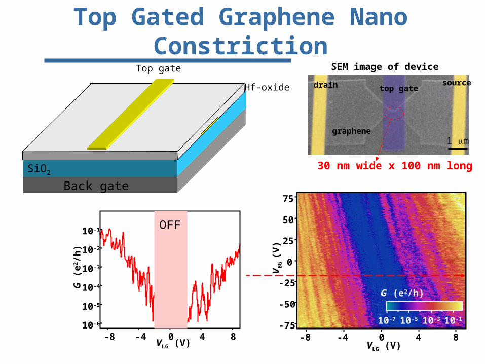
Top Gated Graphene Nano Constriction
source
Back gate
SiO2
drain graphene
-8 -4 0 4 810-6
10-5
10-4
10-3
10-2
10-1
VLG (V)
G (
e2/h
)
OFF
SEM image of device
sourcedrain top gate
graphene1 m
30 nm wide x 100 nm long
Hf-oxide
Top gate

Crystallographic Directional DependenceSon, et al, PRL. 97, 216803 (2006)
2m
0 30 60 900
20
40
Eg (
meV
)
(degree)
Graphene Nanoribbons Edge Effect
Rough Graphene Edge Structures

Localization of Edge Disordered Graphene Nanoribbons
See also:Gunlycke et al, Appl. Phys. Lett. 90 (14), 142104 (2007).Areshkin et al, Nano Lett. 7 (1), 204 (2007)Lherbier et al, PRL 100 036803 (2008)
Querlioz et al., Appl. Phys. Lett. 92, 042108 (2008)
Transport ‘gap’

T-1ln
(R)
3
2
1
0
-1
-2
0.20.10.0
Arrhenius plot
Variable Range Hopping in Graphene Nanoribbons
Con
duct
ance
(S
)
Vg (V)
W = 37 nm
0.1
1
10
100
6040200
4K 15K 100K 200K 300K
E
x
EF
1
1
00max exp
d
T
TGG
d: dimensionality
70 nm
48 nm
37 nm
22 nm15 nm
31 nm3
2
1
0
-1
-2
0.60.40.20.0
ln(R
)
T-1/3
70 nm
48 nm
37 nm
22 nm15 nm
31 nm
2D VRH3
2
1
0
-1
-2
0.40.20.0
ln(R
)
T-1/2
70 nm
48 nm
37 nm
22 nm15 nm
31 nm
1D VRH
T

Rodgers, UIUC
Aligned growth of Nanotubes
Graphene Electronics: ChallengesPros:High mobility High on-off ratioHigh critical current densitySmall channel lengthSmall gate capacitanceLarge Fermi velocity
Con:Controlled growth
Artistic dream (DELFT)
tunability of band gaps
Edge control
This can be turned into advantage:doping site, functionality, and etc…

Graphene Electronics: Conventional & Non-conventional
Conventional Devices
Cheianov et al. Science (07)
Graphene Veselago lense
FETBand gap engineered Graphene nanoribbons
Nonconventional Devices
Trauzettel et al. Nature Phys. (07)
Graphene psedospintronics
Son et al. Nature (07)
Graphene Spintronics
Graphene quantum dot
(Manchester group)

Pd (under HfO2)
Pd (under HfO2)
Pd (over HfO2)
SWCNT (under HfO2)
HfO2 on SiO2/Si+
Carbon Nanotube Superlattice
20 nm
60 nm
1 m
Purewal, Takekosh, Jarillo-Herrero, Kim (2008)
Kouwenhoven PRL (1992)
-54 -50 -45 -40
4
3
2
1
Back Gate (V)
Top Gate (V)
Co
nd
uc
tan
ce
(S
)0
1
1.0 1.5 2.00.0
0.2
dI/d
V (S
)
Top Gate (V)

Klein Tunneling
Transmission coef
Novoselov et al (2006)
Ballistic Quantum Transport in Graphene Heterojunction
n np xpote
ntia
l
Ballistic transport in the barrier
Graphene NPN junctions
Realistic smooth potential distribution
Total Internal Reflection
Cheianov and Fal’ko (2006)
Zhang and Fogler (2008)
Tunneling through smooth pn junction
Requirements forExperimental Observation:
• Long Mean free path -> Ballistic conduction
• Small d -> better collimination
Top gate width: 50 nm < Lm
graphene
electrode
1 m
SEM image of device

Transport Ballistic Graphene Heterojunction
VBG = 90 V
VBG = -90 V
ppp
pnpnpn
nnngraphene
electrode
1 m
Young and Kim (2008)
VTG (V)-10 0-2-4-6-8 0 108642
Conductance (m
S)
6
4
10
8
12
PN junction resistance
Zhang and Fogler (2008)
18 V
-18 V´
L
n1,, k1,
T
TT
RR*
n1,, k1,
n2,, k2
Conductance Oscillation: Fabry-Perot
k1 /k2= sin’ / sin = 2L /cos’
Mean free path~ 200 nm
Junction length< 100 nm
See also Shavchenko et al and Goldhaber-Gordon’s recent preprint

Quantum Oscillations in Ballistic Graphene Heterojunction
ntop (1012 cm2)
n back
(1012
cm
2 )
5-5 0
0
-5
5
0 1-1
dR/dntop ( h/e2 10-15 cm-2)
Resistance Oscillations
0 20 40 60
0
1
-10 -8 -6 -4
85
90
95
100
105
G (
e2 /h)
VTG
(V)
80K 60K 43K 30K 16K 4K
T (K)
Am
pli
tud
e
Oscillation persist high temperature!

ConclusionsConclusions
• Carbon nanotube FET is mature technology demonstrating substantial improvement over Si CMOS
• Controlled growth and scaling up of CNTFET remains as a challenge
• Graphene provides scaling up solution of carbon electronics with high mobility
• Controlled growth of graphene and edge contol remains as a challenge
• Novel quantum device concepts have been demonstrated on graphene and nanontubes