Embed Size (px)
Citation preview

NanoscaleAdvances
PAPER
Ope
n A
cces
s A
rtic
le. P
ublis
hed
on 2
5 Ju
ne 2
021.
Dow
nloa
ded
on 1
0/10
/202
1 1:
44:3
8 PM
. T
his
artic
le is
lice
nsed
und
er a
Cre
ativ
e C
omm
ons
Attr
ibut
ion-
Non
Com
mer
cial
3.0
Unp
orte
d L
icen
ce.
View Article OnlineView Journal | View Issue
Topology design
aState Key Laboratory of Information Photon
University of Posts and Telecommunications,
bupt.edu.cnbCentre for Theoretical and Computational M
Bioengineering and Nanotechnology, The U
4072, Australia. E-mail: mingchao.wang@ucCentre for Articial-Intelligence Nanopho
Computer Engineering, University of Shangh
200093, China. E-mail: qimingzhang@usst.
† Electronic supplementary informa10.1039/d1na00198a
Cite this:Nanoscale Adv., 2021, 3, 4579
Received 16th March 2021Accepted 25th June 2021
DOI: 10.1039/d1na00198a
rsc.li/nanoscale-advances
© 2021 The Author(s). Published by
of digital metamaterials for ultra-compact integrated photonic devices based onmode manipulation†
Han Ye, *a Yanrong Wang,a Shuhe Zhang,a Danshi Wang,a Yumin Liu, a
Mingchao Wang *b and Qiming Zhang*c
Precise manipulation of mode order in silicon waveguides plays a fundamental role in the on-chip all-
optical interconnections and is still a tough task in design when the functional region is confined to
a subwavelength footprint. In this paper, digital metamaterials consisting of silicon and air pixels are
topologically designed by an efficient method combining 2D finite element method for optical
simulations, density method for material description and method of moving asymptotes for optimization.
Only around 150 iterations are required for searching satisfactory solutions. Six high-quality and efficient
conversions between four TE-polarized modes are achieved in a functional region with footprint 0.645l2
(center wavelength l ¼ 1550 nm). Based on asymmetric mode conversion, a reciprocal optical diode
with high contrast ratio is further obtained with the optimization starting from TE0-to-TE1 mode
converter. Moreover, we successfully design a 1 � 2 demultiplexer with footprint 1.0l2 and demonstrate
a simple mode division multiplexing system with satisfactory performances. Finally, by changing the
refractive index to an equivalent value, quasi-3D designs are obtained and the functionalities are
validated in 3D simulations for both free-standing and SOI configurations.
1. Introduction
Manipulation of mode order in silicon waveguides has attractedextensive attention in terms of acting as promising buildingblocks in novel applications, such as on-chip all-optical diodesand mode division multiplexing systems.1–5 Several conven-tional schemes have been proposed to achieve mode orderconversion in waveguides, which include interferometer,6–8 two-dimensional photonic crystal structure,9–13 metasurface,14
deformed silicon waveguide,15 partial etching,16–18 direct wave-guide coupling5,19 and sub-wavelength grating coupling.20,21
However, the footprints of the reported photonic devices basedon the above mentioned schemes are mostly around 5 to 10microns and even larger. A compact structure as an essentialattribute should be highly emphasized in integrated photonicdevices. In recent years, methods involving topology
ics and Optical Communications, Beijing
Beijing 100876, China. E-mail: Han_ye@
olecular Science, Australian Institute for
niversity of Queensland, St Lucia, QLD
q.edu.eu
tonics, School of Optical-Electrical and
ai for Science and Technology, Shanghai
edu.cn
tion (ESI) available. See DOI:
the Royal Society of Chemistry
optimization have been put forward in order to reduce thefootprint and avoid design obstacles due to the lack of knownunderlying mechanisms.22–24 The distribution of materials withrefractive index contrast inside the compact functional regioncan be obtained by topology optimization via two distinctstrategies: ordinary optimization and objective-rst optimiza-tion. In ordinary optimization, the problem is to minimize theobjective function accounting for the desired mode conversionstep by step, while the governing equations, i.e. Maxell's equa-tions, are always satised in each iteration.11–13 On the contrary,satisfying of the objective is kept prior to the governing equa-tions in the objective-rst strategy, and the optimization is usedto nd the solution which minimizes the physical residue.25,26
Following these two strategies, the search of optimal materialdistribution can be performed using ether gradient-basedalgorithms or non-gradient-based algorithms.27–29 Moreover,from the geometric perspective, the targeted material distribu-tions possess either complex continuous pattern11–13,30 or pixe-lated pattern (also referred to as metastructure or digitalmetamaterial).28,29 The description of continuous shape needsadditional efforts like the geometric projection method andsmoothing method. The pixelated ones with nanoscale pixelsare easier to describe in simulation and fabricate in experiment.
Although great efforts have been made toward designingultra-compact mode converters, precise conversions between allsupportedmode orders in a single waveguide are rarely reportedin the literature.25,31 A pioneer work was reported by Lu et al.25
Nanoscale Adv., 2021, 3, 4579–4588 | 4579
Nanoscale Advances Paper
Ope
n A
cces
s A
rtic
le. P
ublis
hed
on 2
5 Ju
ne 2
021.
Dow
nloa
ded
on 1
0/10
/202
1 1:
44:3
8 PM
. T
his
artic
le is
lice
nsed
und
er a
Cre
ativ
e C
omm
ons
Attr
ibut
ion-
Non
Com
mer
cial
3.0
Unp
orte
d L
icen
ce.
View Article Online
using an objective-rst algorithm. The footprints of functionalregions were achieved as 1.55 square vacuum wavelengths withcontinuous relative permittivity inside. When consideringa limiting size of the functional region, i.e. width of the func-tional region is the same as that of the waveguide, such furtherreduction of footprint would bring huge challenges in designdue to the limited space for light interference.25,26 Meanwhile,the speed of convergence in optimization is another importantissue.26 The gradient/sensitivity in gradient-based algorithmscan accelerate the optimization process compared with non-gradient-based algorithms (e.g. direct binary search28,32 andparticle swarm optimization29), especially in cases with a largeamount of design freedom. Recently, machine learning hasbeen adopted to design nanophotonic devices such as a powersplitter.33 However, for a large amount of pixels and for suchcomplicated mode conversion functionality, a huge dataset isrequired and only a purely random dataset may not be sufficientto obtain effective inverse design. Moreover, important appli-cations based on mode conversion, e.g. optical diodes26,32 andmode demultiplexers,34,35 are still being pursued to be achievedin a more highly compact functional region, while majorperformances like mode purity, insertion loss and contrast ratioare not compromised.
In this paper, ultra-compact integrated digital metamaterialsfor mode order manipulation, reciprocal unidirectional trans-mission and mode division multiplexing are demonstrated.Combining nite element method (FEM), density method (DM)and method of moving asymptotes (MMA), we efficiently obtainthese high-quality inverse designs in around only 150 iterations.The functional regions of mode converter and optical diode are0.645l2 in terms of footprint, while the value of mode divisionmultiplexer is 1.0l2.
2. Design and method
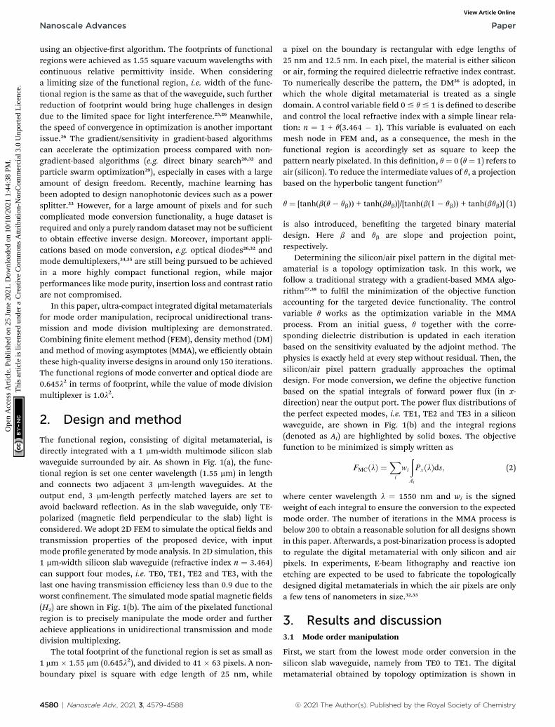
The functional region, consisting of digital metamaterial, isdirectly integrated with a 1 mm-width multimode silicon slabwaveguide surrounded by air. As shown in Fig. 1(a), the func-tional region is set one center wavelength (1.55 mm) in lengthand connects two adjacent 3 mm-length waveguides. At theoutput end, 3 mm-length perfectly matched layers are set toavoid backward reection. As in the slab waveguide, only TE-polarized (magnetic eld perpendicular to the slab) light isconsidered. We adopt 2D FEM to simulate the optical elds andtransmission properties of the proposed device, with inputmode prole generated by mode analysis. In 2D simulation, this1 mm-width silicon slab waveguide (refractive index n ¼ 3.464)can support four modes, i.e. TE0, TE1, TE2 and TE3, with thelast one having transmission efficiency less than 0.9 due to theworst connement. The simulated mode spatial magnetic elds(Hz) are shown in Fig. 1(b). The aim of the pixelated functionalregion is to precisely manipulate the mode order and furtherachieve applications in unidirectional transmission and modedivision multiplexing.
The total footprint of the functional region is set as small as1 mm � 1.55 mm (0.645l2), and divided to 41 � 63 pixels. A non-boundary pixel is square with edge length of 25 nm, while
4580 | Nanoscale Adv., 2021, 3, 4579–4588
a pixel on the boundary is rectangular with edge lengths of25 nm and 12.5 nm. In each pixel, the material is either siliconor air, forming the required dielectric refractive index contrast.To numerically describe the pattern, the DM36 is adopted, inwhich the whole digital metamaterial is treated as a singledomain. A control variable eld 0# q# 1 is dened to describeand control the local refractive index with a simple linear rela-tion: n ¼ 1 + q(3.464 � 1). This variable is evaluated on eachmesh node in FEM and, as a consequence, the mesh in thefunctional region is accordingly set as square to keep thepattern nearly pixelated. In this denition, q¼ 0 (q¼ 1) refers toair (silicon). To reduce the intermediate values of q, a projectionbased on the hyperbolic tangent function37
q ¼ [tanh(b(q � qb)) + tanh(bqb)]/[tanh(b(1 � qb)) + tanh(bqb)] (1)
is also introduced, beneting the targeted binary materialdesign. Here b and qb are slope and projection point,respectively.
Determining the silicon/air pixel pattern in the digital met-amaterial is a topology optimization task. In this work, wefollow a traditional strategy with a gradient-based MMA algo-rithm27,38 to full the minimization of the objective functionaccounting for the targeted device functionality. The controlvariable q works as the optimization variable in the MMAprocess. From an initial guess, q together with the corre-sponding dielectric distribution is updated in each iterationbased on the sensitivity evaluated by the adjoint method. Thephysics is exactly held at every step without residual. Then, thesilicon/air pixel pattern gradually approaches the optimaldesign. For mode conversion, we dene the objective functionbased on the spatial integrals of forward power ux (in x-direction) near the output port. The power ux distributions ofthe perfect expected modes, i.e. TE1, TE2 and TE3 in a siliconwaveguide, are shown in Fig. 1(b) and the integral regions(denoted as Ai) are highlighted by solid boxes. The objectivefunction to be minimized is simply written as
FMCðlÞ ¼Xi
wi
ð
Ai
PxðlÞds; (2)
where center wavelength l ¼ 1550 nm and wi is the signedweight of each integral to ensure the conversion to the expectedmode order. The number of iterations in the MMA process isbelow 200 to obtain a reasonable solution for all designs shownin this paper. Aerwards, a post-binarization process is adoptedto regulate the digital metamaterial with only silicon and airpixels. In experiments, E-beam lithography and reactive ionetching are expected to be used to fabricate the topologicallydesigned digital metamaterials in which the air pixels are onlya few tens of nanometers in size.32,33
3. Results and discussion3.1 Mode order manipulation
First, we start from the lowest mode order conversion in thesilicon slab waveguide, namely from TE0 to TE1. The digitalmetamaterial obtained by topology optimization is shown in
© 2021 The Author(s). Published by the Royal Society of Chemistry
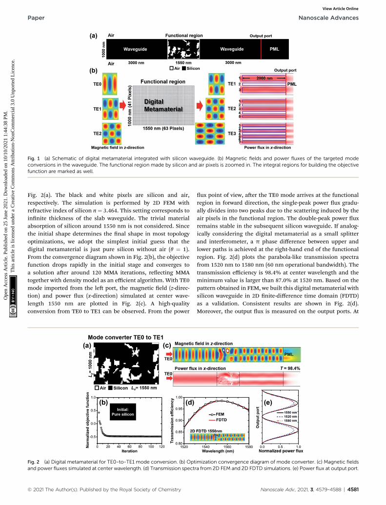
Fig. 1 (a) Schematic of digital metamaterial integrated with silicon waveguide. (b) Magnetic fields and power fluxes of the targeted modeconversions in the waveguide. The functional region made by silicon and air pixels is zoomed in. The integral regions for building the objectivefunction are marked as well.
Paper Nanoscale Advances
Ope
n A
cces
s A
rtic
le. P
ublis
hed
on 2
5 Ju
ne 2
021.
Dow
nloa
ded
on 1
0/10
/202
1 1:
44:3
8 PM
. T
his
artic
le is
lice
nsed
und
er a
Cre
ativ
e C
omm
ons
Attr
ibut
ion-
Non
Com
mer
cial
3.0
Unp
orte
d L
icen
ce.
View Article Online
Fig. 2(a). The black and white pixels are silicon and air,respectively. The simulation is performed by 2D FEM withrefractive index of silicon n ¼ 3.464. This setting corresponds toinnite thickness of the slab waveguide. The trivial materialabsorption of silicon around 1550 nm is not considered. Sincethe initial shape determines the nal shape in most topologyoptimizations, we adopt the simplest initial guess that thedigital metamaterial is just pure silicon without air (q ¼ 1).From the convergence diagram shown in Fig. 2(b), the objectivefunction drops rapidly in the initial stage and converges toa solution aer around 120 MMA iterations, reecting MMAtogether with density model as an efficient algorithm. With TE0mode imported from the le port, the magnetic eld (z-direc-tion) and power ux (x-direction) simulated at center wave-length 1550 nm are plotted in Fig. 2(c). A high-qualityconversion from TE0 to TE1 can be observed. From the power
Fig. 2 (a) Digital metamaterial for TE0-to-TE1 mode conversion. (b) Optand power fluxes simulated at center wavelength. (d) Transmission spectr
© 2021 The Author(s). Published by the Royal Society of Chemistry
ux point of view, aer the TE0 mode arrives at the functionalregion in forward direction, the single-peak power ux gradu-ally divides into two peaks due to the scattering induced by theair pixels in the functional region. The double-peak power uxremains stable in the subsequent silicon waveguide. If analog-ically considering the digital metamaterial as a small splitterand interferometer, a p phase difference between upper andlower paths is achieved at the right-hand end of the functionalregion. Fig. 2(d) plots the parabola-like transmission spectrafrom 1520 nm to 1580 nm (60 nm operational bandwidth). Thetransmission efficiency is 98.4% at center wavelength and theminimum value is larger than 87.0% at 1520 nm. Based on thepattern obtained in FEM, we built this digital metamaterial withsilicon waveguide in 2D nite-difference time domain (FDTD)as a validation. Consistent results are shown in Fig. 2(d).Moreover, the output ux is measured on the output ports. At
imization convergence diagram of mode converter. (c) Magnetic fieldsa from 2D FEM and 2D FDTD simulations. (e) Power flux at output port.
Nanoscale Adv., 2021, 3, 4579–4588 | 4581

Fig. 4 Transmission spectra of six mode converters.
Nanoscale Advances Paper
Ope
n A
cces
s A
rtic
le. P
ublis
hed
on 2
5 Ju
ne 2
021.
Dow
nloa
ded
on 1
0/10
/202
1 1:
44:3
8 PM
. T
his
artic
le is
lice
nsed
und
er a
Cre
ativ
e C
omm
ons
Attr
ibut
ion-
Non
Com
mer
cial
3.0
Unp
orte
d L
icen
ce.
View Article Online
center wavelength, the shapes of output uxes satisfactorilyreproduce the shapes of standard TE1 modes. At 1520 nm and1580 nm, only small distortions unavoidably occur. The resultsindicate that the performance of the digital metamaterial ob-tained from optimization at only center wavelength is accept-able and no additional optimization for expanding operationalbandwidth is required.
The adopted 1 mm-width silicon waveguide supports four TEmodes. Compared with TE0 to TE1 mode conversion shownabove, the precise conversion between specic modes is a morecomplicated task but desirable as well. Since only linear mate-rials (silicon and air) are considered, the functional region isa linear device following time-reversal symmetry. In this sense,we need to explore six digital metamaterials for all possibleconversions between these four modes. The proposed topologyoptimization method is easily extended to this task withoutmodication, but only with a new objective function for thetargeted mode. The obtained digital metamaterials for modeconversions, including TE0 to TE1, TE0 to TE2, TE0 to TE3, TE1to TE2, TE1 to TE3 and TE2 to TE3, are plotted in Fig. 3(a). Todemonstrate the functionality, we plot the simulated magneticelds at center wavelength in Fig. 3(b) and the correspondingtransmission efficiencies are also listed. For conversions to TE1and TE2, the transmission efficiencies are higher than 95%,while for conversions to TE3, the values are in the rangebetween 85% and 89%. This decrease does not come from theinsertion of digital metamaterials, but the less connement ofTE3. As shown in Fig. 4, the transmission spectra withina 60 nm operational bandwidth indicate that these topologicallydesigned digital metamaterials are broadband high-qualitymode converters. The performances presented are comparablewith those of the designs in ref. 25 while the binary design inour work consists of only air and silicon pixels. The amounts ofair and silicon pixels inside the proposed functional regions arelisted in Table S1.† Moreover, one should note the inuence ofpixel size on the topology design of a photonic device. Largerpixel size inside the digital metamaterials can reduce the
Fig. 3 (a) Digital metamaterials for six mode conversions. (b) Magnetic fi
4582 | Nanoscale Adv., 2021, 3, 4579–4588
challenges for experimental fabrication, but decrease the designfreedom which may sacrice the performance and even lead tofailure to nd a design for such complicated mode manipula-tion. Since we aim to achieve high performance in the func-tional region with footprint (in length) below 1550 nm and keepthe number of pixels to an integer, a 25 nm pixel size is chosen.This value is comparable with the design units with length l/40in ref. 25 and 26. As a comparison, TE0-to-TE1 and TE0-to-TE2mode converters are redesigned with 50 nm pixel size, as shownin Fig. S1.† It can be seen that both transmission efficiency andmode purity are slightly lower, but still acceptable.
3.2 Reciprocal unidirectional transmission
The unidirectional transmission of light in a silicon waveguidehas attracted huge interest in the last decade, especially theschemes based on linear and passive integrated devices.2,8–10,26
Due to the linear regime, time-reversal symmetry is held. Suchdevices are naturally not optical isolators but optical diodes forspecic modes. The underlying mechanism is simply asym-metric mode conversion which relies on the precise control ofmode order or polarization. Based on the obtained mode orderconversion results, the digital metamaterial for optical diodes
elds of six mode converters simulated at center wavelength.
© 2021 The Author(s). Published by the Royal Society of Chemistry

Fig. 5 (a) Digital metamaterial for optical diode. (b) Optimization convergence diagram of optical diode starting from TE0-to-TE1 modeconverter. (c) Forward and backward magnetic fields and power fluxes simulated at center wavelength.
Paper Nanoscale Advances
Ope
n A
cces
s A
rtic
le. P
ublis
hed
on 2
5 Ju
ne 2
021.
Dow
nloa
ded
on 1
0/10
/202
1 1:
44:3
8 PM
. T
his
artic
le is
lice
nsed
und
er a
Cre
ativ
e C
omm
ons
Attr
ibut
ion-
Non
Com
mer
cial
3.0
Unp
orte
d L
icen
ce.
View Article Online
can be further pursued. We only focus on the unidirectionaltransmission of the TE0 mode as an exemplary case. In thisscheme, the TE0 mode is expected to be converted to the TE1mode in the forward direction, while in the backward direction,the TE0 mode will be forbidden to transmit through the func-tional region. Therefore, we start with the TE0-to-TE1 designshown in Fig. 2(a). The forward conversion is already achievedand needs to be kept. The only modication is an additionalterm in the new objective function which can be expressed as
FdiodeðlÞ ¼ FforwðlÞ þ FbackðlÞ
¼Xfi
wfi
ð
Afi
PforwðlÞdsþ wb
ðPbackwðlÞds: (3)
The integral of backward power ux is simpler because we onlyneed to eliminate the light in this direction.
The topologically designed digital metamaterial for unidi-rectional transmission of TE0 is shown in Fig. 5(a). Startingfrom the mode converter, the optimization uses about 160iterations to be converged to an optical diode. Again, the MMA
Fig. 6 Forward and backward transmission spectra of optical diode.
© 2021 The Author(s). Published by the Royal Society of Chemistry
algorithm shows high efficiency by the rapid decrease of theobjective function in the initial stage. With the TE0 modeimported from le and right port, the magnetic eld (z-direc-tion) and power ux (x-direction) simulated at center wave-length of 1550 nm are plotted in Fig. 5(c). As expected, TE0 isconverted to TE1 in forward direction with transmission effi-ciency Tf ¼ 98.2%, while this value for TE0 in backward direc-tion is only Tb ¼ 0.15%. The contrast ratio, dened as rc ¼ (Tf �Tb)/(Tf + Tb), reaches 0.997. When considering the unidir-ectionality dened as U ¼ 10 log10(Tf/Tb), the peak value isapproximately 28 dB, which is higher than that of our previousdesigns based on photonic crystals12,13 and surface plasmonics.8
If TE1 is excited at the right-hand port, TE1 is converted back toTE0 in the backward direction. It can be seen that the magneticelds are nearly identical between the uppermost and lower-most plots in Fig. 5(c), conrming the time-reversal symmetryin this reciprocal optical diode. As shown in Fig. 6, the forwardtransmission efficiency keeps higher than 92.6% from 1520 nmto 1580 nm, while the value keeps lower than 0.37% in thebackward direction. Theminimum contrast ratio is 0.992 (24 dBunidirectionality) within the 60 nm operational bandwidth.
3.3 Mode division multiplexing
Besides reciprocal unidirectional transmission, mode divisionmultiplexing (MDM) is another promising application ofprecise mode order manipulation, which enhances the trans-mission capacity of on-chip optical interconnection from anadditional dimension to the wavelength.19,21,32,39 Each modeinside the bus waveguide carries information individually, evenat identical wavelength. Here, we focus on topologicallydesigning a compact 1 � 2 demultiplexer. As shown in Fig. 7,the footprint of the demultiplexer is set as small as 1.55 mm �1.55 mm (1.0l2) and divided to 63 � 63 pixels. The size of eachpixel is the same as described in previous sections. The multi-mode bus waveguide is set at 1 mm in width to support at leasttwomodes, and the two output waveguides, with Port A and Port
Nanoscale Adv., 2021, 3, 4579–4588 | 4583

Fig. 7 (a) Digital metamaterial for 1 � 2 demultiplexer. (b) Optimization convergence diagram of demultiplexer. (c) Magnetic fields and powerfluxes simulated at center wavelength with TE0 and TE1 modes imported in bus waveguide.
Nanoscale Advances Paper
Ope
n A
cces
s A
rtic
le. P
ublis
hed
on 2
5 Ju
ne 2
021.
Dow
nloa
ded
on 1
0/10
/202
1 1:
44:3
8 PM
. T
his
artic
le is
lice
nsed
und
er a
Cre
ativ
e C
omm
ons
Attr
ibut
ion-
Non
Com
mer
cial
3.0
Unp
orte
d L
icen
ce.
View Article Online
B, are set at 0.4 mm in width. The demultiplexer routes a certainmode to a certain output waveguide, based on which theobjective function is built and can be expressed as
FdemultiðlÞ ¼ FTE0ðlÞ þ FTE1ðlÞ
¼ wTE0-A
ðPAðlÞdsþ wTE0-B
ðPBðlÞds
þ wTE1-A
ðPAðlÞdsþ wTE1-B
ðPBðlÞds: (4)
To avoid the impact of an initial guess, the topology optimiza-tion starts with the simplest conguration, namely a puresilicon region without air.
The digital metamaterial obtained for the demultiplexer isplotted in Fig. 7(a). Starting from pure silicon, it takes theoptimization process about 130 iterations to converge toa demultiplexer. Since the objective function is quite differentand more complicated, the general applicability of the adoptedmethod combing FEM, DM and MMA is well demonstrated. Asshown by the magnetic eld and power ux distributions inFig. 7(c), when the TE0 mode is transmitted in the bus wave-guide, the light is routed to the upper waveguide. The trans-mission efficiencies measured at Port A and Port B are 91.8%and 0.04%, respectively. On the contrary, when the TE1 mode istransmitted in the bus waveguide, the light is routed to thelower waveguide. The transmission efficiencies are 0.10% and89.1% for Port A and Port B, respectively. These FEM simula-tions are performed at center wavelength of 1550 nm. Thecorresponding contrast ratios are respectively 0.999 and 0.998,indicating the satisfactory performance of this demultiplexer.
To further demonstrate the functionality and evaluate theperformance, it behooves us to build anMDM system. As shownin Fig. 8(a), from le to right, the MDM system is composed of
4584 | Nanoscale Adv., 2021, 3, 4579–4588
two input waveguides, a multiplexer, a bus waveguide,a demultiplexer and two output waveguides. Since the digitalmetamaterial consists of only linear silicon and air, the multi-plexer can be obtained by simply mirroring the design of thedemultiplexer due to the reciprocal feature. In this scheme, theupper waveguides (Port A and Port C) form a channel, while theother two (Port B and Port D) form another channel. TE0 andTE1 modes in the bus waveguide are individually utilized as thecarriers for these two channels. The magnetic elds simulatedat the center wavelength of 1550 nm are plotted in Fig. 8(a). Iflight is imported from Port A and passes the multiplexer, theTE0 mode is excited and transmits in the bus waveguide, andthen the demultiplexer routes the light to Port C. The trans-mission efficiencies measured at Port C, Port B and Port D are85.4%, 0.05% and 0.08%, respectively. When we consider theother channel carried by the TE1 mode, the transmission effi-ciencies measured at Port D, Port A and Port C are 84.0%, 0.13%and 0.10%, respectively. The contrast ratio accounting forchannel crosstalk is 0.998 for the TE0 channel and 0.997 for theTE1 channel, reecting a good performance of the MDMsystem. Within a 60 nm operational bandwidth, the trans-mission spectra measured at the ports are plotted in Fig. 8(b)and (c) for TE0 and TE1 channels, respectively. No obviousdegradation is observed.
3.4 Quasi-3D designs
The proposed topology optimization method combining DMandMMA needs to run with 2D FEM simulation at the moment.In previous sections, the refractive index of silicon is set at n ¼3.464, which corresponds to innite thickness of the slabwaveguide. When the thickness of the waveguide reduces,a blue shi of the transmission spectrum is expected due to thereduction of effective refractive index. To maintain the same
© 2021 The Author(s). Published by the Royal Society of Chemistry

Fig. 8 (a) Schematic of an MDM system and corresponding magnetic fields simulated at center wavelength. (b) Transmission spectra with inputfrom Port A. (c) Transmission spectra with input from Port B.
Paper Nanoscale Advances
Ope
n A
cces
s A
rtic
le. P
ublis
hed
on 2
5 Ju
ne 2
021.
Dow
nloa
ded
on 1
0/10
/202
1 1:
44:3
8 PM
. T
his
artic
le is
lice
nsed
und
er a
Cre
ativ
e C
omm
ons
Attr
ibut
ion-
Non
Com
mer
cial
3.0
Unp
orte
d L
icen
ce.
View Article Online
operational wavelength range (1520 nm to 1560 nm) for a realdevice integrated with a 340 nm thick silicon slab wave-guide,11,30 the refractive index of silicon in 2D FEM simulation(denoted as quasi-3D) has to be reduced to an equivalent value n¼ 3.0, determined by a tedious trial-and-error approach. We re-perform the topology optimizations for TE0-to-TE1 modeconverter, optical diode and demultiplexer with exactly samestrategies. The newly obtained quasi-3D designs are plotted inFig. 9(a). Despite the silicon and air patterns being differentfrom those of previous sections due to the change of refractiveindex of silicon, the major performances remain similar, asshown in Fig. 9(b) and (c).
In experiments, E-beam lithography and reactive ion etchingare needed to fabricate such inversely designed digital meta-materials whose length of pixels is at the nanometer scale.Major error may occur in both material and shape of thesesquare pixels. Instead of square, a circular shape of air hole isintroduced to avoid the edge distortion in some recentdesigns.34,35 Unfortunately, this treatment only suits the inversedesign strategy for predened pixels and is not compatible withthe adopted DM in which the distribution of dielectric materialis described by a single design variable. In this sense, weassume the shape of a pixel is perfect and focus on the wrongmaterial for the pixel as the fabrication error. To account forthis kind of error, pixels with wrong material are randomlyintroduced to the quasi-3D designs for optical diode anddemultiplexer. The relation between performances and theerror percentage are demonstrated in Figs. S2 and S3.† Eightdiode samples and ve demultiplexer samples are simulated for
© 2021 The Author(s). Published by the Royal Society of Chemistry
each error percentage from 2% to 5%. As can be seen, 3% errorcan be acceptable for both devices, indicating the robustness ofthe proposed designs.
Finally, a 3D FDTD simulation is performed to validate thefunctionalities and performances of the quasi-3D designs. Thethickness of waveguide and digital metamaterials is set at340 nm.11,30 Two cases are considered: free-standingmodels andmodels sitting on top of a SiO2 layer without cladding layer(denoted as SOI). The sizes of monitors used to collect theoutput light are set exactly the same as the waveguide cross-section. Additionally, we give a test for 2D FDTD simulationswith n ¼ 3.0 rst. Consistent results with 2D FEM simulationsare obtained if comparing the transmission spectra plotted inFig. 9 and 10. For 3D TE0-to-TE1 mode converter, the trans-mission efficiencies remain higher than 49% for both free-standing and SOI cases, while the values at center wavelengthare 60.3% and 52.7%, respectively. As shown in the inset ofFig. 10(a), the output power ux at 1550 nm has two clear andseparated peaks, indicating acceptable quality of the conversionto the TE1 mode. For the optical diode, the contrast ratiosbetween forward and backward directions respectively keephigher than 0.983 (20.6 dB unidirectionality) and 0.972 (18.4 dBunidirectionality) for free-standing and SOI cases, which arehigher than for previously reported pixelated inversedesigns.26,32 As shown by the spectra plotted in Fig. 10(c) and (d),the demultiplexer clearly routes the power of the TE0 mode andTE1 mode to Port A and Port B, respectively. The contrast ratiosbetween the two output ports keep higher than 0.9 within the60 nm operational bandwidth for all cases. Generally, the
Nanoscale Adv., 2021, 3, 4579–4588 | 4585

Fig. 9 (a) Digital metamaterials of quasi-3D designs. (b) Transmission spectra of mode converter and optical diode. (c) Transmission spectra ofdemultiplexer with TE0 and TE1 modes as input.
Nanoscale Advances Paper
Ope
n A
cces
s A
rtic
le. P
ublis
hed
on 2
5 Ju
ne 2
021.
Dow
nloa
ded
on 1
0/10
/202
1 1:
44:3
8 PM
. T
his
artic
le is
lice
nsed
und
er a
Cre
ativ
e C
omm
ons
Attr
ibut
ion-
Non
Com
mer
cial
3.0
Unp
orte
d L
icen
ce.
View Article Online
performances of free-standing models are slightly better thanthose of SOI models. Detailed comparisons between theproposed mode converter, optical diode and demultiplexer withreported designs are listed in Tables S2–S5.† Moreover, themagnetic elds measured on the center cross-section of 3D
Fig. 10 Transmission spectra from 2D and 3D FDTD simulations (free-stDemultiplexer with TE0 mode input. (d) Demultiplexer with TE1 modemodels.
4586 | Nanoscale Adv., 2021, 3, 4579–4588
models are nearly identical to those from 2D simulations at thesame wavelength, providing a validation of such quasi-3Ddesign strategy. However, 3D FDTD results are still facingdegradation. The links between 2D optimization and 3Dsimulation still need to be further investigated.
anding and SOI). (a) TE0-to-TE1 mode converter. (b) Optical diode. (c)input. (e) Magnetic fields observed on the center cross-section of 3D
© 2021 The Author(s). Published by the Royal Society of Chemistry

Paper Nanoscale Advances
Ope
n A
cces
s A
rtic
le. P
ublis
hed
on 2
5 Ju
ne 2
021.
Dow
nloa
ded
on 1
0/10
/202
1 1:
44:3
8 PM
. T
his
artic
le is
lice
nsed
und
er a
Cre
ativ
e C
omm
ons
Attr
ibut
ion-
Non
Com
mer
cial
3.0
Unp
orte
d L
icen
ce.
View Article Online
4. Conclusions
In summary, we proposed ultra-compact designs for modeorder manipulation in a silicon waveguide based on digitalmetamaterials consisting of silicon and air pixels. All functionalregions obtained by topologically designing are below square ofcenter wavelength in terms of footprint. Six mode orderconversions between TE0, TE1, TE2 and TE3 in a 1 mm-widthwaveguide with high efficiency and high mode purity arerstly demonstrated. Based on the forward TE0-to-TE1 modeconversion, a reciprocal optical diode is further obtained byadding an additional objective in optimization to block the TE0mode in backward direction. Moreover, with the same method,we design a 1 � 2 demultiplexer for TE0 and TE1 modes ina bus waveguide, and demonstrate a simple MDM system withsatisfactory performances. Finally, the functionalities are vali-dated by 3D FDTD simulations. We expect that the proposedwaveguide-integrated digital metamaterials for mode ordermanipulation can play important roles in on-chip all-opticalinterconnections.
Author contributions
HY – conceptualization, methodology, formal analysis, fundingacquisition, writing – original dra; YW – formal analysis; SZ –
writing – review and editing; DW – writing – review and editing;YL – writing – review and editing; MW – conceptualization,writing – review and editing; QZ – funding acquisition, writing –review and editing.
Conflicts of interest
There are no conicts to declare.
Acknowledgements
The nancial support of this work is from the National NaturalScience Foundation of China (no. 61975123, 61671090) andFund of State Key Laboratory of Information Photonics andOptical Communications (Beijing University of Posts and Tele-communications), PR China (IPOC2020ZT01).
References
1 D. Jalas, A. Petrov, M. Eich, W. Freude, S. Fan, Z. Yu, R. Baets,M. Popovic, A. Melloni, J. D. Joannopoulos,M. Vanwolleghem, C. R. Doerr and H. Renner, What is -and what is not - an optical isolator, Nat. Photonics, 2013,7, 579.
2 V. Liu, D. A. B. Miller and S. Fan, Ultra-compact photoniccrystal waveguide spatial mode converter and itsconnection to the optical diode effect, Opt. Express, 2012,20, 28388.
3 L. Luo, N. Ophir, C. P. Chen, L. H. Gabrielli, C. B. Poitras,K. Bergmen and M. Lipson, WDM-compatible mode-division multiplexing on a silicon chip, Nat. Commun.,2014, 5, 3069.
© 2021 The Author(s). Published by the Royal Society of Chemistry
4 D. Dai, J. Wang and Y. Shi, Silicon mode (de)multiplexerenabling high capacity photonic networks-on-chip witha single-wavelength-carrier light, Opt. Lett., 2013, 38, 1422.
5 D. Garcia-Rodriguez, J. L. Corral, A. Griol and R. Llorente,Dimensional variation tolerant modeconverter/multiplexerfabricated in SOI technology for two-mode transmission at1550 nm, Opt. Lett., 2017, 42, 1221.
6 B. B. Oner, K. Ustun, H. Kurt, A. K. Okyay and G. Turhan-Sayan, Large bandwidth mode order converter bydifferential waveguides, Opt. Express, 2015, 23, 3186.
7 B. T. Lee and S. Y. Shin, Mode-order converter ina multimode waveguide, Opt. Lett., 2003, 28, 1660.
8 J. Li, H. Ye, Z. Yu and Y. Liu, Design of a broadbandreciprocal optical diode in a silicon waveguide assisted bysilver surface plasmonic splitter, Opt. Express, 2017, 25,19129.
9 C. Wang, C. Z. Zhou and Z. Y. Li, On-chip optical diode basedon silicon photonic crystal heterojunctions, Opt. Express,2011, 19, 26948.
10 S. Feng and Y. Wang, Unidirectional reciprocal wavelengthlters based on the square-lattice photonic crystalstructures with the rectangular defects, Opt. Express, 2013,21, 220.
11 L. H. Frandsen, Y. Elesin, L. F. Frellsen, M. Mitrovic, Y. Ding,O. Sigmund and K. Yvind, Topology optimized modeconversion in a photonic crystal waveguide fabricated insilicon-on insulator material, Opt. Express, 2014, 22, 8525.
12 H. Ye, Z. Yu, Y. Liu and Z. Chen, Realization of compactbroadband optical diode in linear air-hole photonic crystalwaveguide, Opt. Express, 2016, 24, 24592.
13 H. Ye, D. Wang, Z. Yu, J. Zhang and Z. Chen, Ultra-compactbroadband mode converter and optical diode based onlinear rod-type photonic crystal waveguide, Opt. Express,2015, 23, 9673.
14 Z. Y. Li, M. H. Kim, C. Wang, Z. H. Han, S. Shrestha,A. C. Overvig, M. Lu, A. Stein, A. M. Agarwal, M. Loncarand N. F. Yu, Controlling propagation and coupling ofwaveguide modes using phase-gradient metasurfaces, Nat.Nanotechnol., 2017, 12, 675.
15 D. Chen, X. Xiao, L. Wang, Y. Yu, W. Liu and Q. Yang, Low-loss and fabrication tolerant silicon mode order convertersbased on novel compact tapers, Opt. Express, 2015, 23,11152.
16 D. Ohana, D. Boris, N. Mazurski and U. Levy, Dielectricmetasurface as a platform for spatial mode conversion innanoscale waveguides, Nano Lett., 2016, 16, 7956.
17 D. Ohana and U. Levy, Mode conversion based on dielectricmetamaterial in silicon, Opt. Express, 2014, 22, 27617.
18 D. Zhu, J. Zhang, H. Ye, Z. Yu and Y. Liu, Design ofa broadband reciprocal optical diode in multimode siliconwaveguide by partial depth etching, Opt. Commun., 2018,418, 88.
19 W. Jiang, J. Miao and T. Li, Compact silicon 10-mode multi/demultiplexer for hybrid mode- and polarisation-divisionmultiplexing system, Sci. Rep., 2019, 9, 13223.
Nanoscale Adv., 2021, 3, 4579–4588 | 4587

Nanoscale Advances Paper
Ope
n A
cces
s A
rtic
le. P
ublis
hed
on 2
5 Ju
ne 2
021.
Dow
nloa
ded
on 1
0/10
/202
1 1:
44:3
8 PM
. T
his
artic
le is
lice
nsed
und
er a
Cre
ativ
e C
omm
ons
Attr
ibut
ion-
Non
Com
mer
cial
3.0
Unp
orte
d L
icen
ce.
View Article Online
20 Z. Cheng, J. Wang, Z. Yang, L. Zhu, Y. Yang, Y. Huang andX. Ren, Sub-wavelength grating assisted mode orderconverter on the SOI substrate, Opt. Express, 2019, 27, 34434.
21 Y. He, Y. Zhang, Q. Zhu, S. An, R. Cao, X. Guo, C. Qiu andY. Su, Silicon High-Order Mode (De)Multiplexer on SinglePolarization, J. Lightwave Technol., 2018, 36, 5746.
22 S. Molesky, Z. Lin, A. Y. Piggott, W. Jin, J. Vuckovic andA. W. Rodriguez, Inverse design in nanophotonics, Nat.Photonics, 2018, 12, 659.
23 K. Aydin, Nanostructured silicon success, Nat. Photonics,2015, 9, 353.
24 A. Y. Piggot, J. Lu, K. G. Lagoudakis, J. Petykiewicz,T. M. Babinec and J. Vuckovic, Inverse design anddemonstration of a compact and broadband on-chipwavelength demultiplexer, Nat. Photonics, 2015, 9, 347.
25 J. Lu and J. Vuckovic, Objective-rst design of high-efficiency, small-footprint couplers between arbitrarynanophotonic waveguide modes, Opt. Express, 2012, 20,7221.
26 F. Callewaert, S. Butun, Z. Li and K. Aydin, Inverse design ofan ultra-compact broadband optical diode based onasymmetric spatial mode conversion, Sci. Rep., 2016, 6,32577.
27 K. Svanberg, The method of moving asymptotes-a newmethod for structural optimization, Int. J. Numer. MethodsEng., 1987, 24, 359.
28 B. Shen, P. Wang, R. Polson and R. Menon, An integrated-nanophotonics polarization beamsplitter with 2.4 � 2.4mm2 footprint, Nat. Photonics, 2015, 9, 378.
29 Q. Lu, X. Yan, W. Wei, X. Zhang, M. Zhang, J. Zheng, B. Li,Y. Luo, Q. Lin and X. Ren, High-speed ultra-compact all-optical NOT and AND logic gates designed by a multi-objective particle swarm optimized method, Opt. LaserTechnol., 2019, 116, 322.
30 L. F. Frellsen, Y. Ding, O. Sigmund and L. H. Frandsen,Topology optimized mode multiplexing in silicon-on-
4588 | Nanoscale Adv., 2021, 3, 4579–4588
insulator photonic wire waveguides, Opt. Express, 2016, 24,16866.
31 H. Jia, S. L. Yang, T. Zhou, L. Zhang, T. Wang, H. X. Chen,J. H. Yang and L. Yang, Mode-Oriented PermutationCipher Encryption and Passive Signal Switching Based onMultiobjective Optimized Silicon SubwavelengthMetastructures, ACS Photonics, 2020, 7, 2163.
32 B. Shen, R. Polson and R. Menon, Integrated digitalmetamaterials enables ultra-compact optical diodes, Opt.Express, 2015, 23, 10847.
33 M. H. Tahersima, K. Kojima, T. Koike-Akino, D. Jha,B. N. Wang, C. W. Lin and K. Parsons, Deep NeuralNetwork Inverse Design of Integrated Photonic PowerSplitters, Sci. Rep., 2019, 9, 1368.
34 H. Xie, Y. Liu, S. Wang, Y. Wang, Y. Yao, Q. Song, J. Du, Z. Heand K. Xu, Highly Compact and Efficient Four-ModeMultiplexer Based on Pixelated Waveguides, IEEE PhotonicsTechnol. Lett., 2020, 32, 166.
35 W. Chang, L. Lu, X. Ren, L. Lu, M. Cheng, D. Liu andM. Zhang, An Ultracompact Multimode WaveguideCrossing Based on Subwavelength Asymmetric Y-Junction,IEEE Photonics J., 2018, 10, 4501008.
36 M. P. Bendsøe, Optimal shape design as a materialdistribution problem, Structural Optimization, 1989, 1, 193.
37 F. Wang, B. S. Lazarov and O. Sigmund, On projectionmethods, convergence and robust formulations in topologyoptimization, Struct. Multidiscip. O., 2011, 43, 767.
38 K. Svanberg, A class of globally convergent optimizationmethods based on conservative convex separableapproximations, Siam J. Optimiz., 2002, 12, 555.
39 Y. He, Y. Zhang, H. Wang, L. Sun and Y. Su, Design andexperimental demonstration of a silicon multi-dimensional(de)multiplexer for wavelength-, mode- and polarization-division (de)multiplexing, Opt. Lett., 2020, 45, 2846.
© 2021 The Author(s). Published by the Royal Society of Chemistry