Embed Size (px)
Citation preview
Microelectronic Engineering 142 (2015) 58–63
Contents lists available at ScienceDirect
Microelectronic Engineering
j ourna l homepage: www.e lsev ie r .com/ locate /mee
Top–down fabrication of horizontally-aligned gallium nitride nanowirearrays for sensor development☆
Guannan Liu a,b, Baomei Wen b,c, Ting Xie a,b, Audie Castillo b,c, Jong-Yong Ha a,b, Nichole Sullivan c,Ratan Debnath b,c, Albert Davydov b, Martin Peckerar a, Abhishek Motayed a,b,c,⁎a Department of Electrical and Computer Engineering, University of Maryland, College Park, MD 20742, USAb Material Measurement Laboratory, National Institute of Standards and Technology, Gaithersburg, MD 20899, USAc N5 Sensors, Inc., 9610 Medical Center Drive, Suite 200, Rockville, MD 20850, USA
☆ Certain commercial equipment, instruments, or matein order to specify the experimental procedure adequaintended to imply recommendation or endorsementStandards and Technology, nor is it intended to imply thidentified are necessarily the best available for the purpos⁎ Corresponding author at: Department of Electrica
University of Maryland, College Park, MD 20742, USA.E-mail address: [email protected] (A. Motay
http://dx.doi.org/10.1016/j.mee.2015.08.0040167-9317/© 2015 Elsevier B.V. All rights reserved.
a b s t r a c t
a r t i c l e i n f oArticle history:Received 14 November 2014Received in revised form 4 August 2015Accepted 7 August 2015Available online 12 August 2015
Keywords:Gallium nitrideNanowireTop–down approachSurface treatmentSensors
This paper demonstrates a high-throughput fabrication method of gallium nitride (GaN) nanowire (NW)and sub-micron wire (SMW) arrays using a combination of projection lithography, plasma etching, and post-plasma wet etching techniques. Photoluminescence (PL), field emission scanning electron microscopy(FESEM), and I–V measurements were used to characterize the GaN NW/SMW devices. These NWs/SMWs canbe used to create highly-sensitive and selective conductometric chemical/bio-sensors.The length and width of the wires can be precisely customized. The length of the NW/SMW varied from 5 μm to5 mm and the width ranges from 100 nm to 500 nm. Such comprehensive control in the geometry of a wire isdifficult to achieve with other fabrication methods. The post-plasma KOH wet etching greatly reduces the surfaceroughness of theGaNNW/SMWaswell as the performance of devices. Complementarymetal-oxide-semiconductor(CMOS) andmicro-electro-mechanical system (MEMS) devices can be incorporatedwith GaNNW/SMWarrays ona single chip using this top–down fabrication method.
© 2015 Elsevier B.V. All rights reserved.
1. Introduction
Gallium nitride (GaN) is a versatile semiconductor used in opticaldevices (light-emitting diodes, laser diodes, UV sensors) and in powerelectronics (power switches, RF devices, and high power transistors)[1]. Due to its direct band gap and chemical and thermal stability, GaNnanowires (NWs) are gaining significant importance as chemical sensorelements [2–4].
To date, most of GaN NWs devices are fabricated using chemicalvapor deposition growth with a follow-up detachment from the sub-strate and individual on-chip alignment. Due to the variation in mor-phology, dimensions, doping, and crystal quality, it is hard to controlthe quality of NWs grown via the bottom–up methods [5]. Besides,variations from a multi-step pick-and-place fabrication process resultin a low yield of functioning devices. Thus, such a process has lowlarge-area integration capabilities, rendering mass-manufacturing
rials are identified in this papertely. Such identification is notby the National Institute ofat the materials or equipmente.l and Computer Engineering,
ed).
challenging. An alternative approach to overcome these drawbacks isthe top–down fabrication, in which NWs are patterned on a uniformthin-film using standard lithography and etching. Vertically-alignedsemiconductor NWs (nanorods, nanopillars or nanocolumns) havebeen demonstrated by such top–down methods [6–10]. The heights ofthese nanostructures are limited by the thickness of the starting thin-film material, and they often exhibit tapering as a result of etching.On the contrary, horizontally-aligned NWs can be fabricated withoutany length limitations. For photodetectors and photovoltaic devices,vertically-aligned nanowires represent a high efficiency platform,whereas for chemical sensors horizontally-aligned nanowires arethe optimal choice [11–13]. Due to its inherent inertness to most wetchemical etches, GaN nanostructures are commonly produced usingdry etch techniques [8]. However, high-aspect ratio GaN structuresachieved by plasma etching are often associated with extensive sidewall damage, result in lower performance of the device [14]. Therefore,producing damage-free nitride structures with a precisely-defined ge-ometry over large area remains a challenge.
By combining deep-UV projection lithography and inductively-coupled plasma (ICP) etching, this paper demonstrates horizontally-aligned NWs etched from a GaN thin film grown on sapphire. Sincethe rough and tapered NW sidewalls due to dry etching create leakagecurrent and limit NWperformance [14], a post ICP potassiumhydroxide(KOH) wet etching procedure was developed to smooth the NW walls.

Fig. 1. Schematic representation of the nanowire fabrication process flow. (1) RCAcleaning of GaN on sapphire wafer, (2) SiN etch-mask deposited using PECVD, (3) spin-coating of photo-resist stack of LOR3A and Ultra-I, (4) lithography and development,(5) metal deposition by e-beam evaporator, (6) lift-off in 1165 photo-resist remover,(7) ICP etching to transfer the pattern on GaN, (8) HF etching, RIE etching to removemetal and SiN etch masks, followed by subsequent KOH wet etch treatment.
Fig. 3. ICP etch depth as a function of the etch time. The original data are shown by blackdots, and a liner fit to the data shown by the solid green line. (For interpretation of thereferences to color in this figure legend, the reader is referred to the web version of thisarticle.)
59G. Liu et al. / Microelectronic Engineering 142 (2015) 58–63
The KOH etching also allows us to control the final shape and dimen-sions of the NWs. The PL and current–voltage (I–V) results verify theimproved performance resulting from the KOH treatment.
The top–down approach described here can potentially enable GaNNW and SMW to be integrated with LED, micro-pumps, and microheaters for system-on-chip development [15–20]. Different types ofsensors such as chemical, gas and bio sensors can be fabricated usingthe top–down method reported here.
2. Fabrication
Two different thicknesses of commercial intrinsic GaN epitaxiallayers (NTT Advanced Technology) grown on c-plane sapphire wereused in this study: 3 μm thick GaN films were used for characterizationof the etch rate of ICP dry etching, optimization ofwet etching andmea-surements of PL spectra; 1 μm thick GaN films were used in the optimi-zation of the wet etching process as well as in I–V characterization.AlGaN is a buffer layer widely used to compensate lattice mismatchand reduce stress in the growing film, and thereby improves the crystal-line quality of GaN on sapphire. In our experiment, a 500 nm AlGaN
Fig. 2. (a) SEM image of single nanowire device. The total length is 5000 μm and width of 5magnification SEM image of the same nanowire with 30° tilt. (b) Final packaged device for ph
layer was used between the GaN and sapphire substrate. A silicon ni-tride (SiN) passivation layer with thickness of 50 nm was depositedby plasma enhanced chemical vapor deposition (PECVD). This layerpreventsmetal penetration into the bulk GaN. A bi-layer stack of photo-resist (MicroChem LOR3A andUltra-i) was spun onto thewafer for pho-tolithographypatterning. The 570mJ/cm2 stepper lithographydosewasoptimized for the fabrication process.
A bi-layer metal stack (50 nm Ti and 120 nm Ni) was deposited bye-beam evaporator (Denton Infinity 22) and lifted-off. This was follow-ed by ICP etching (Oxford Plasmalab 100) with a combination gases(Cl/N2/Ar 25/5/1 sccm) at 40 °C temperature, 300 W RF power and800 W ICP power. After removal of Ti/Ni metal shadow mask and SiN,potassium hydroxide (KOH) wet etching was studied at various tem-peratures (40 °C, 60 °C, and 80 °C) and in different solvents (deionizedwater, isopropanol, and ethylene glycol), and for different etchingtimes from 10 min to 5 h. The fabrication steps for NW formation areshown in Fig. 1. PLmeasurements and SEM imagingwere conducted be-fore and after KOH etching as well as on the control sample (pristineGaN film). The optimized condition of KOH treatment (10% KOH in eth-ylene glycol etching for 2 h at 80 °C) was used on NWs. An ohmic con-tact metal stack (Ti/Al/Ti/Au) was deposited by e-beam evaporationfor I–V characterization of the samples. The electrical properties of theno KOH treatment control group and a 2 h KOH etched group withdifferent length NWswere studied. Due to the highly resistive propertyof intrinsic GaN, I–Vmeasurements were conducted under UV (355 nmwavelength, 48 μW/cm2 intensity) illumination. The width of both
00 nm. The upper inset shows the identical NW arrays. The lower inset shows a higherotoconductance testing, a single die shown in the inset contains 81 NWs devices.

Fig. 4. SEM images of a nanowire section after ICP etch. (a) plan-view, (b) 45° tilted. The top surface appears smooth, however sidewall damage is evident.
60 G. Liu et al. / Microelectronic Engineering 142 (2015) 58–63
multiple parallel NWs and single meander-shape NW arrays presentedin this paper was 500 nm. By stepper lithography (ASML PAS5500) op-timization, we were able to pattern MWs with width ranging from200 nm to 300 nm. The final width after KOH wet etching was 100 nm.
3. Results and discussion
Fig. 2(a) shows SEM image of the longest length (5000 μm) wire inthemeander-shape. The upper inset of Fig. 2(a) shows a lowmagnifica-tion image of 6 identical NWs. The lower inset of Fig. 2(a) shows a highmagnification of a NW. Thewire bondedNWs in a chip carrier for IV andphotoconductance measurement are shown in Fig. 2(b). On a singlechip, the total 9 groups of NW arrays with length range from 10 μm to5000 μm were fabricated. And within each group, there are 9 identicalNWs arranged in a 3 × 3 matrix.
Several GaN layers (3 μm thickness) were ICP etched for differenttimes to calibrate the etch rate. The etched thickness was measured bya profilometer and the data summary is shown in Fig. 3. Black dotsshow the original data, and the regression linearization analysis (greenline) gives the dry etching rate of 428.9 nm/min. Based on this rate, an3 min etching was performed on the 1 μm GaN/500 nm AlGaN films tofabricate the nanowire devices.
Both top view and tilted SEM images of NWs after ICP etching areshown in Fig. 4. The vertical texture on the sidewalls formed by plasmabombardment is clearly seen in this figure. To remove the surfacedefects, KOH wet etching methods are explored with different etchingtemperatures, solvent compositions and times.
Fig. 5. Room-temperature PLmeasurement of GaNNWs. The pristine film before ICP etch-ing (black line); after ICP etching (red line); and post-ICP KOH etching for 10 min at 40 °C(blue line), 60 °C (green line) and 80 °C (purple line). All the graphs are normalized by thenear-band edge (355 nm) emission intensity. (For interpretation of the references to colorin this figure legend, the reader is referred to the web version of this article.)
3.1. Wet etching temperatures
The samples were etched for 10 min in a 10% KOH in deionizedwater (DIW) solution at 40 °C, 60 °C and 80 °C. PL measurementswere conducted before and after KOH etching as well as on the controlsample (pristine GaN film). In Fig. 5, intensities are normalized with re-spect to peaks at near-band edge (NBE) of 355 nm. Surface defects arecreated during the ICP etch, which are non-radiative recombinationcenters, results in the decreasing of the NBE emission compared to theimpurity-related PL peaks at 420 nm and 600 nm. The subsequentKOH etch removes the ICP-damaged layers from the sidewall surfacesand remarkably reduces the surface non-radiative recombination cen-ters density. After etching at 80 °C, the overall shape of the PL spectrumof GaNNWsurface resembles that of the pristine GaN film surface. Sim-ilar results also observed and reported on by Q. Li et al. [9].
3.2. Wet etching solvents
The 10% KOH in DIW etchant used above shows the improvement ofPL intensity at 80 °C. However, the KOH in DIW shows aggressive etch-ing of the a-plane of GaN, leading to an anisotropic etching profile asshown in the first column of Fig. 6. To address this issue, three differenttypes of etch baths, namely 10%KOH inDIW, isopropanol (IPA) and eth-ylene glycol (EG), were studied in order to find a truly isotropic etch,one that is more controllable when used in batch fabrication.
All three groups were studied under the same conditions: 10 minetching at 80 °C. PL measurements were conducted after treatment.These results are similar to those shown in Fig. 5 (purple line). SEMimages (Fig. 6) reveal different etching rates of different facets: for thetop surfaces (c-plane) of GaN NWs, etching was not observable for allthree cases. The sidewalls of the NWs (a-plane and m-plane) werefound to be more easily attacked by KOH.
Generally speaking, the a-plane is less stable than m-plane due to ahigher surface energy [21,22], so the etch rate is faster on a-plane thanon the m-plan. SEM images (Fig. 6) show NWs disconnected at severalpoints after etching with KOH in DIW, while m-plane NWs remain thesame. Thus, we conclude KOH in DIW etches a-plane much faster thanthe other solutions. A high reaction rate is not favorable in achievingthe smooth etched surfaces [23,24]. An organic solvent addition, suchas IPA or EG, slows down the a-plane etching process and making itcomparable in rate to m-plane etching in order to achieve “isotropic”etching. The organic solvent contained in the solution plays an impor-tant role in the etching process. The organicmolecules ofwill selectivelyadhere to some crystallographic planes (a-plane in our case), therebyhindering the access of etching agent (KOH) and slowing down thecorresponding plane's etching rate. KOH in IPA etching shows an im-provement in the isotropy of the etch process. IPA can slow down theetch rate of a-plane. However, it still etches faster than the m-plane.KOH in EG etching shows the most isotropic result since both a-planeandm-plane end upwith the sameNWwidth. Both the first and second

Fig. 6. SEM images of NWs after KOH in different solvents. The first row indicates the a-plane and m-plane wires under study. The second row shows the conjoined parts. This is a shorta-plane NW connects two m-plane NWs. For DIW and IPA solvents, a-plane NWs were over-etched and disconnected after treatment. Blue dash lines indicate the original NW sidewallpositions before the treatment. Yellow dash lines indicate that the final sidewall position after treatment. The m-planes replaced the original a-plane at the inner loop of the part becauseof a higher etch rate on the a-plane (in contrast to them-plane.) For the EG solvent, NWswere not severely etched after the treatment. This result shows that the KOH in EG solvent is thebest candidate for isotropic etching among the three explored. (For interpretation of the references to color in this figure legend, the reader is referred to the web version of this article.)
61G. Liu et al. / Microelectronic Engineering 142 (2015) 58–63
columns of Fig. 6 highlight the original NW sidewalls before treatmentby blue dashed lines. It is obvious that the a-plane etches faster thanm-plane NWs in DIW and IPA. The high magnification image of the
Fig. 7. SEM images of NWs after KOH in EG treatments. (a)–(d) correspond to different etchin(c) and (d) indicate the original NW sidewall position before the treatment. Yellow dash linesinterpretation of the references to color in this figure legend, the reader is referred to the web
90° bend parts proves this fact. The inner side of the NWs is etchedto m-planes with 120° inter-planar angles between them. This ishighlighted by the yellow dashed line in these figures. These results
g times from 10 min to 3 h under condition of 10% KOH in EG at 80 °C. Blue dash lines inin (c) and (d) indicate the interface between GaN and AlGaN layers after treatment. (Forversion of this article.)
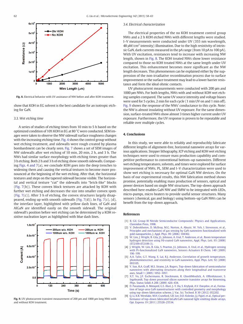
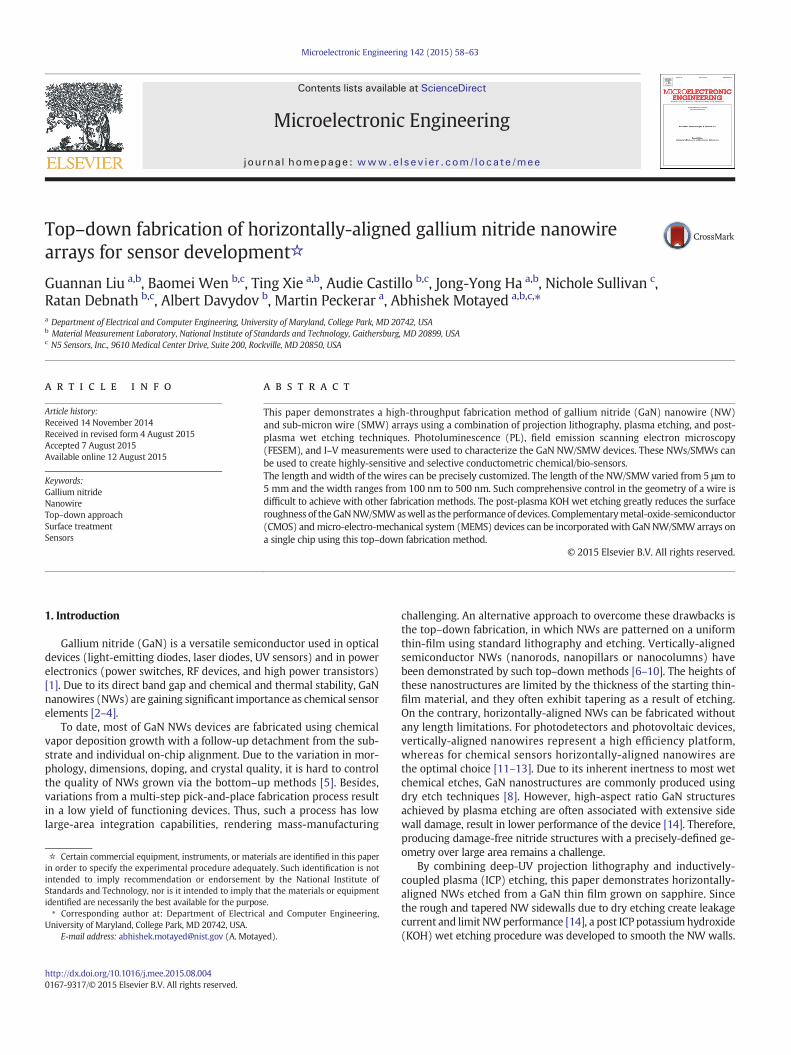
Fig. 8. Electrical behavior with UV assistance of NW before and after KOH treatment.
62 G. Liu et al. / Microelectronic Engineering 142 (2015) 58–63
show that KOH in EG solvent is the best candidate for an isotropic etch-ing for GaN.
3.3. Wet etching time
A series of studies of etching times from 10 min to 5 h based on theoptimized condition of 10%KOH in EG at 80 °Cwere conducted. SEM im-ages were taken to observe the NW sidewall surface roughness changeswith the increasing etching time. Fig. 4 shows the control groupwithoutwet etching treatment, and sidewalls were rough created by plasmabombardment can be clearly seen. Fig. 7 shows a set of SEM images ofNW sidewalls after wet etching of 10 min, 20 min, 2 h, and 3 h. TheNWs had similar surface morphology with etching times greater than3h etching. Both2 h and 3h of etching show smooth sidewalls. Compar-ing Figs. 4 and 7(a), we conclude KOH goes into the deep trenches towidening them and causing the vertical textures to become more pro-nounced at the beginning of the wet etching. After that, the horizontaltextures and steps on the tapered sidewall become visible. The horizon-tal and vertical texture “cut” the sidewalls into “brick-like” blocks(Fig. 7(b)). These convex block textures are attacked by KOH withfurther wet etching and decreases the size into smaller convex spots(Fig. 7(c)). After 3 h of etching, the convex structures largely disap-peared, ending up with smooth sidewalls (Fig. 7(d)). In Fig. 7(c), (d),the interface layer, highlighted with yellow dash lines, of GaN andAlGaN are identified easily on the smooth sidewall. The originalsidewall's position before wet etching can be determined by a KOH re-sistive nucleation layer as highlighted with blue dash lines.
Fig. 9. UV photocurrent transient measurement of 200 μm and 1000 μm long NWs withand without KOH treatment.
3.4. Electrical characterization
The electrical properties of the no KOH treatment control groupNWs and a 2 h KOH etched NWs with different lengths were studied.I–V measurements were conducted under UV (355 nm wavelength,48 μW/cm2 intensity) illumination. Due to the high resistivity of intrin-sic GaN, dark currentsmeasured in the pA range (from10pA to 100pA).With UV excitation, resistances tend to increase with increasing NWlength, shown in Fig. 8. The KOH treated NWs show lower resistancecompared to those no KOH treated NWs at the same length under UVexcitation. This enhancement becomes more significant as the NWlength decreases. This phenomenon can be explained either by the sup-pression of the non-irradiative recombination process due to surfaceimprovement or the surface treatmentmay lead to a lower barrier resis-tance and form the ideal ohmic contacts.
UV photocurrent measurements were conducted with 200 μm and1000 μmNWs. For both lengths, NWs with and without KOH wet etch-ing samples compared. The sameUV source intensity and voltage biaseswere used for 5 cycles, 2min for each cycle (1min UV on and 1min off).Fig. 9 shows the response of the NWs' conductance to this cycle. Note:the NW is almost insulating without UV exposure. For the same dimen-sion, surface-treatedNWs show almost 3 times higher current underUVexposure. Furthermore, the UV response is proven to be repeatable andreliable over multiple cycles.
4. Conclusions
In this study, we were able to reliably and reproducibly fabricatedifferent lengths of alignment-free, horizontal nanowire arrays for var-ious applications. Stepper lithography, ICP etching and KOHwet etchingtechniques were used to ensure mass production capability and com-petitive performance to conventional bottom–up nanowires. Differentwet etching temperatures, solvents, and timeswere explored for surfaceimprovement of NWs. PL, SEM and I–V characterization were used toshow wet etching is necessary for optimal GaN NW devices. On thebasis of our experimental results, this NW fabrication method showspromise, potentially enabling mass production of sensors, optical andpower devices based on single NW structures. The top–down approachdescribed here enables GaN NW and SMW to be integrated with LEDs,micro-pumps, micro heaters to provide useful sensor structures. Manysensors (chemical, gas and biology) using bottom–up GaN NWs can bebenefit from the top–down approach.
References
[1] B. Gil, Group III Nitride Semiconductor Compounds: Physics and Applications,Clarendon Press, 1998.
[2] V. Dobrokhotov, D. McIlroy, M.G. Norton, A. Abuzir, W. Yeh, I. Stevenson, et al.,Principles and mechanisms of gas sensing by GaN nanowires functionalized withgold nanoparticles, J. Appl. Phys. 99 (2006) 104302.
[3] W. Lim, J. Wright, B. Gila, J.L. Johnson, A. Ural, T. Anderson, et al., Room temperaturehydrogen detection using Pd-coated GaN nanowires, Appl. Phys. Lett. 93 (2008)(072109-072109-3).
[4] J. Wright, W. Lim, B. Gila, S. Pearton, J.L. Johnson, A. Ural, et al., Hydrogen sensingwith Pt-functionalized GaN nanowires, Sensors Actuators B Chem. 140 (2009)196–199.
[5] A.A. Talin, G.T. Wang, E. Lai, R.J. Anderson, Correlation of growth temperature,photoluminescence, and resistivity in GaN nanowires, Appl. Phys. Lett. 92 (2008)093105.
[6] Y. Sun, R.A. Graff, M.S. Strano, J.A. Rogers, Top–down fabrication of semiconductornanowires with alternating structures along their longitudinal and transverseaxes, Small 1 (2005) 1052–1057.
[7] X.T. Vu, J.F. Eschermann, R. Stockmann, R. GhoshMoulick, A. Offenhäusser, S.Ingebrandt, Top–down processed silicon nanowire transistor arrays for biosensing,Phys. Status Solidi A 206 (2009) 426–434.
[8] D. Paramanik, A. Motayed, G.S. Aluri, J.-Y. Ha, S. Krylyuk, A.V. Davydov, et al., Forma-tion of large-area GaN nanostructures with controlled geometry and morphologyusing top–down fabrication scheme, J. Vac. Sci. Technol. B 30 (2012) 052202.
[9] Q. Li, K.R. Westlake,M.H. Crawford, S.R. Lee, D.D. Koleske, J.J. Figiel, et al., Optical per-formance of top–down fabricated InGaN/GaN nanorod light emitting diode arrays,Opt. Express 19 (2011) 25528–25534.

63G. Liu et al. / Microelectronic Engineering 142 (2015) 58–63
[10] Q. Li, J.B. Wright, W.W. Chow, T.S. Luk, I. Brener, L.F. Lester, et al., Single-mode GaNnanowire lasers, Opt. Express 20 (2012) 17873–17879.
[11] Y. Cui, Q. Wei, H. Park, C.M. Lieber, Nanowire nanosensors for highly sensitive andselective detection of biological and chemical species, Science 293 (2001)1289–1292.
[12] P. Offermans, M. Crego-Calama, S.H. Brongersma, Gas detection with vertical InAsnanowire arrays, Nano Lett. 10 (2010) 2412–2415.
[13] G. Sberveglieri, C. Baratto, E. Comini, G. Faglia, M. Ferroni, A. Ponzoni, et al., Synthesisand characterization of semiconducting nanowires for gas sensing, Sensors Actua-tors B Chem. 121 (2007) 208–213.
[14] C.-Y. Wang, L.-Y. Chen, C.-P. Chen, Y.-W. Cheng, M.-Y. Ke, M.-Y. Hsieh, et al., GaNnanorod light emitting diode arrays with a nearly constant electroluminescentpeak wavelength, Opt. Express 16 (2008) 10549–10556.
[15] G.S. Aluri, A. Motayed, A.V. Davydov, V.P. Oleshko, K.A. Bertness, N.A. Sanford, et al.,Methanol, ethanol and hydrogen sensing using metal oxide and metal (TiO2–Pt)composite nanoclusters on GaN nanowires: a new route towards tailoring the selec-tivity of nanowire/nanocluster chemical sensors, Nanotechnology 23 (2012)175501.
[16] G.S. Aluri, A. Motayed, A.V. Davydov, V.P. Oleshko, K.A. Bertness, N.A. Sanford, et al.,Highly selective GaN-nanowire/TiO2-nanocluster hybrid sensors for detection ofbenzene and related environment pollutants, Nanotechnology 22 (2011) 295503.
[17] C.-P. Chen, A. Ganguly, C.-Y. Lu, T.-Y. Chen, C.-C. Kuo, R.-S. Chen, et al., Ultrasensitivein situ label-free DNA detection using a GaN nanowire-based extended-gate field-effect-transistor sensor, Anal. Chem. 83 (2011) 1938–1943.
[18] R. Chen, C. Lu, K. Chen, L. Chen, Molecule-modulated photoconductivity and gain-amplified selective gas sensing in polar GaN nanowires, Appl. Phys. Lett. 95(2009) 233119.
[19] J.L. Johnson, Y. Choi, A. Ural, W. Lim, J. Wright, B. Gila, et al., Growth and characteriza-tion of GaN nanowires for hydrogen sensors, J. Electron. Mater. 38 (2009) 490–494.
[20] G. Liu, D.A. Lowy, A. Kahrim, C. Wang, Z. Dilli, N. Kratzmeier, et al., A low cost micro-heater for aerosol generation applications, Microelectron. Eng. 129 (2014) 46–52.
[21] J.E. Northrup, J. Neugebauer, Theory of GaN (10 1¯ 0) and (11 2¯ 0) surfaces, Phys.Rev. B 53 (1996) R10477.
[22] Q. Sun, C.D. Yerino, B. Leung, J. Han, M.E. Coltrin, Understanding and controllingheteroepitaxy with the kinetic Wulff plot: a case study with GaN, J. Appl. Phys.110 (2011) 053517.
[23] I. Zubel, I. Barycka, K. Kotowska, M. Kramkowska, Silicon anisotropic etching in alka-line solutions IV: the effect of organic and inorganic agents on silicon anisotropicetching process, Sensors Actuators A Phys. 87 (2001) 163–171.
[24] I. Zubel, M. Kramkowska, The effect of isopropyl alcohol on etching rate and rough-ness of (1 0 0) Si surface etched in KOH and TMAH solutions, Sensors Actuators APhys. 93 (2001) 138–147.


![The production of horizontally aligned single …1. Introduction Since the landmark paper on carbon nanotubes (CNTs) by Iij-ima in 1991 [1], they have attracted widespread attention](https://img.dokumen.tips/doc/110x75/5f1039b57e708231d4480f5b/the-production-of-horizontally-aligned-single-1-introduction-since-the-landmark.jpg)