Embed Size (px)
Citation preview

Development of a Pulsed High VoltageGenerator for Plasma-Immersion Ion
Implantation
A thesis submitted in partial fulfillment of the requirementfor the degree of Bachelor of Science in
Physics from William and Mary in Virginia,
by
M. Brennen Brown
Advisor: Prof. William Cooke
Prof. Dennis Manos
Prof. Todd Averett
Williamsburg, VirginiaMay 7th, 2021
Todd Averett
Contents
Abstract ii
1 Introduction 1
2 Theory 32.1 Pulse Timing and Output Requirements . . . . . . . . . . . . . . . . . . . . 32.2 Electronics for a Pulsed Marx Generator . . . . . . . . . . . . . . . . . . . . 4
2.2.1 Semiconductor-Based Marx Generator . . . . . . . . . . . . . . . . . 42.2.2 MOSFET Operation . . . . . . . . . . . . . . . . . . . . . . . . . . . 52.2.3 Recharge Time and Pulse Period . . . . . . . . . . . . . . . . . . . . 7
2.3 Simulation Software . . . . . . . . . . . . . . . . . . . . . . . . . . . . . . . 112.4 Lab equipment . . . . . . . . . . . . . . . . . . . . . . . . . . . . . . . . . . 12
3 Experimental Findings 133.1 Driving the MOSFET . . . . . . . . . . . . . . . . . . . . . . . . . . . . . . 14
3.1.1 Floating Gate Voltage . . . . . . . . . . . . . . . . . . . . . . . . . . 153.1.2 Zener Gate Voltage . . . . . . . . . . . . . . . . . . . . . . . . . . . . 183.1.3 Self-Driving MOSFETs Using Zeners . . . . . . . . . . . . . . . . . . 19
4 Results 224.1 Circuit Testing . . . . . . . . . . . . . . . . . . . . . . . . . . . . . . . . . . 22
5 Conclusion 28
i

Abstract
This report describes the production of a high voltage Marx Generator for
plasma-immersed ion implantation (PIII). This process can yield multiple surface-level
physical and chemical property changes. For a Plasma Immersion-type implantation,
acceleration of the plasma into a metal’s surface occurs under a pulsed high-voltage
DC bias applied to the sample. This pulsed bias will derived from a Marx Generator,
using pulse-controlled high-voltage transistors (MOSFETs) to switch between the
charging and discharging phases. In this experiment, we have successfully developed
and refined a generator that is able to output high negative voltage in a pulsed fashion.

Chapter 1
Introduction
Ion Implantation is a method by which plasma ions are accelerated into a target,
embedding these ions into the target’s surface molecular matrix without altering
the composition of the target itself. These embedded ions cause physical, chemical,
and electrical property changes at the surface site. This process is most commonly
associated with semiconductor doping, treating a metal with specific deformities to
control its electrical properties. This process can be done using virtually any element,
and can even be used to implant metals into other metals, even if the two are not
mutually soluble. It’s been demonstrated that Ion Implantation can produce materials
with enhanced microhardness and wear properties [3]. These respectively refer to a
material’s resistance to small/thin penetrations and resistance to loss of material due
to abrasion and use, overall promoting integrity and lifetime.
Plasma-Immersion Ion Implantation (PIII) is a specific method of implanting ions
into a target material. The process for conducting PIII involves introducing a plasma
through a radio-frequency (RF) plasma source. Then, a highly negative DC voltage
is applied to the target material, accelerating positive ions from the plasma and into
the surface of the target. In our case, a sufficient vacuum system for producing a
plasma is already set up, but the DC voltage is not. The penetration depth of the
ions is dependent on the voltage established, requiring tens to hundreds and in some
1
cases thousands of Kilovolts for the intended implantation depth of up to several
nanometers [3].
Our primary interest behind the Plasma-Immersion method is in its capacity to
treat a large surface area of a sample. Rather than having a specific target area
blasted by an ion acceleration gun, PIII applies an electric field across the breadth of
the surface of the conductive material. This makes it potentially far more effective
at treating materials with a large surface area. It’s also flexible in both the working
ion energies, and in applying treatment to non-flat objects.
To conduct Ion Implantation, generally three systems are needed: an ion source,
a method of ion acceleration, and a target chamber. In the specific case of PIII, the
ion source and target are held within the same containment chamber. This method
addresses many of the shortcomings of traditional Ion Implantation, particularly the
line-of-sight restrictions on the ion beams used. Additionally, our lab already contains
a High-Vacuum System fitted for RF plasma emission. The method of ion acceleration
is the electric potential gradient produced by a highly negative DC power supply in
connection with the conductive sample.
The plasma-immersion implantation process necessarily requires the DC source
to be pulsed. A pulsed mode of operation suppresses unipolar arcs from forming at
the conductor’s surface. Otherwise, craters form and eject portions of the substrate
as the high-temperature electrons interact with the conductive metal. Additionally,
pulsing prevents excessive electric loads to the power supply and lowers thermal load
applied to the substrate. For keeping these loads small, typical duty cycles are at
about 1% [7][1]. Thus, for creating a PIII apparatus we need a high negative voltage
DC source that can pulse on and off with high frequency.
This paper describes the development of this pulsed high voltage generator, presenting
its principle reasoning, the steps taken to reach a complete assembly, and its performance.
2

Chapter 2
Theory
2.1 Pulse Timing and Output Requirements
The time length needed for our high voltage pulse must be sufficient to both drive
away electrons formed near the substrate’s surface, and long enough to accelerate the
ions within the Debye sheath that forms (area of electron-deficiency in a plasma) into
the target [?]. This is on the scale of microseconds, typically ranging from 0.5 µs to
40 µs. Longer periods are certainly possible, but risk damaging the surface through
accumulated charge.
As for the voltage requirement, it must be large enough to accelerate the ions
quick enough within the time frame of the pulse, and enough to accelerate them
to a high speed such that implantation will actually occur. Many papers which
detail this process use a range between -10kV and -100kV [4], [2], [1]. The time
length of the pulse and its voltage are the two main requirements for the output,
and dictate the parameters of the components used in the final configuration of the
pulse generator. Two other factors, amperage and frequency/ rep rate, dictate the
efficiency of implantation as a factor of time.
3
2.2 Electronics for a Pulsed Marx Generator
Our research began by referencing a report [9] which described a setup for a Marx
Generator for controlled High-Voltage pulses. The principle behind a Marx Generator
involves two phases: a charging phase during which capacitors get charged in parallel
by a supplying voltage, and a discharging phase during which the circuit switches to
align the capacitors in series. Each capacitor holds a set amount of charge, and thus
a set voltage difference across it. When a charged capacitor is newly referenced to a
lower voltage on its ’high’ end, its ’low’ end experiences a voltage drop corresponding
to its charged voltage difference. Thus, by connecting several charged capacitors in
series you can get a stepped-up or stepped-down voltage. This is a concept frequently
seen in charge pumps. In a traditional Marx Generator, this is done using spark-gaps
to switch between parallel and series operation. However, this traditional method
is limited in efficiency and repetition rate. There is also a lack of pulse control for
determining the timing of the spark gaps. 2.1 demonstrates this approach.
2.2.1 Semiconductor-Based Marx Generator
To overcome the issues of a traditional Marx Generator, semiconductors can be used
to operate between charging and discharging modes. [5] Here, the charging and
discharging modes occur depending on when the transistor receives a pulse and
begins to conduct current. Common transistors for this purpose are MOSFETs
(Metal Oxide Silicon Field-Effect Transistor) and IGBTs (Insulated-Gate Bipolar
Transistor). Most other transistor types are intended for lower voltage operation,
and don’t have sufficient breakdown voltage rating for high-voltage multiplication.
Between the two useful transistor types, IGBTs tend to have greater tolerance for
high-voltage applications, but MOSFETs produce better high-frequency switching
responses with lower rise and fall times.
4
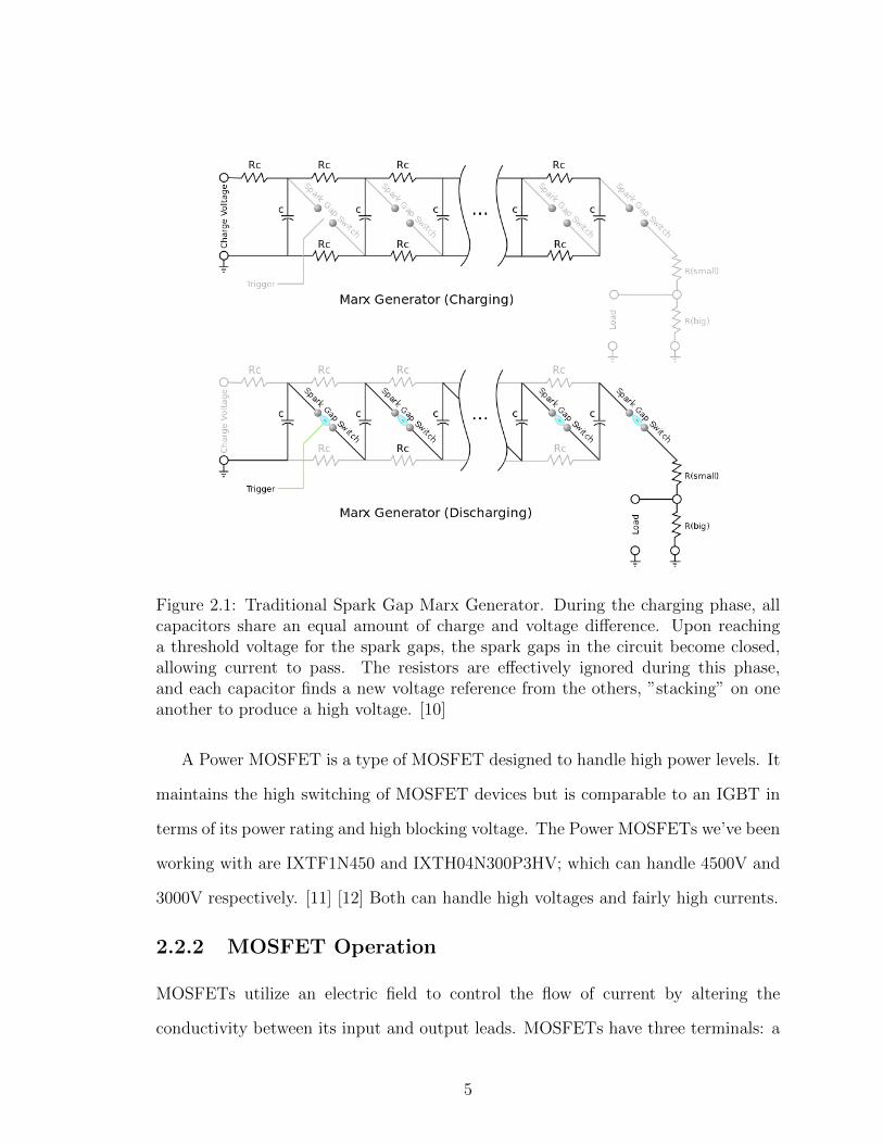
Figure 2.1: Traditional Spark Gap Marx Generator. During the charging phase, allcapacitors share an equal amount of charge and voltage difference. Upon reachinga threshold voltage for the spark gaps, the spark gaps in the circuit become closed,allowing current to pass. The resistors are effectively ignored during this phase,and each capacitor finds a new voltage reference from the others, ”stacking” on oneanother to produce a high voltage. [10]
A Power MOSFET is a type of MOSFET designed to handle high power levels. It
maintains the high switching of MOSFET devices but is comparable to an IGBT in
terms of its power rating and high blocking voltage. The Power MOSFETs we’ve been
working with are IXTF1N450 and IXTH04N300P3HV; which can handle 4500V and
3000V respectively. [11] [12] Both can handle high voltages and fairly high currents.
2.2.2 MOSFET Operation
MOSFETs utilize an electric field to control the flow of current by altering the
conductivity between its input and output leads. MOSFETs have three terminals: a
5
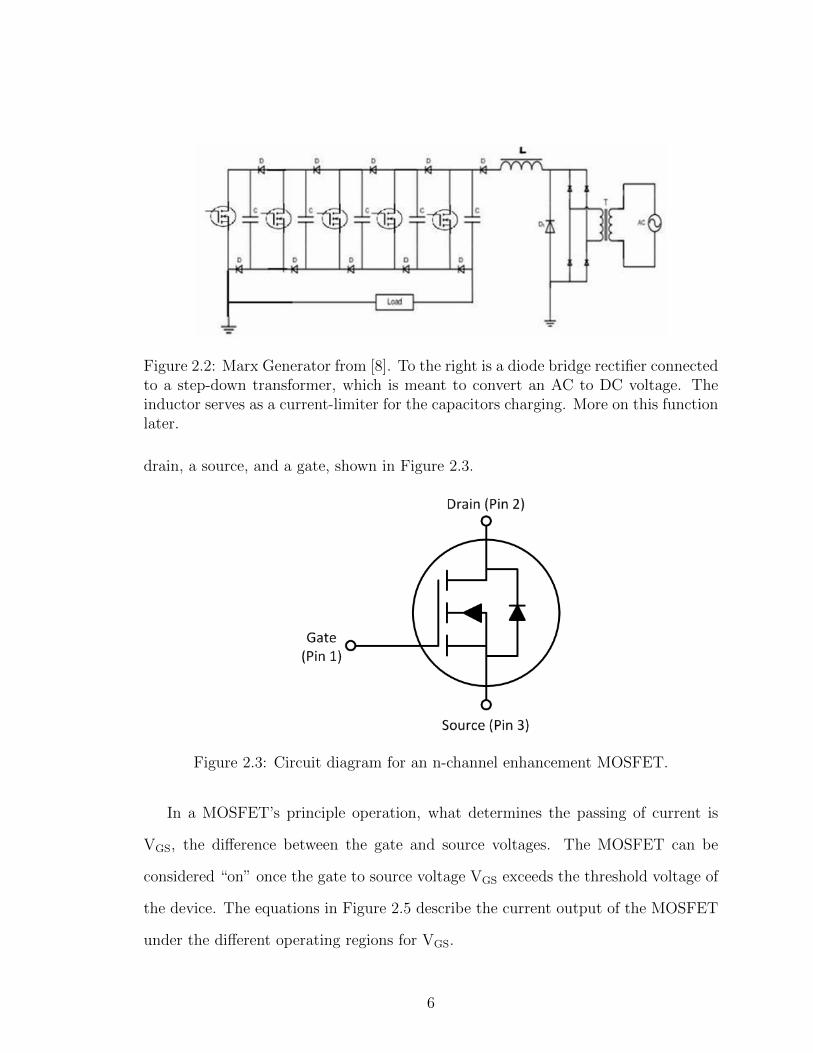
Figure 2.2: Marx Generator from [8]. To the right is a diode bridge rectifier connectedto a step-down transformer, which is meant to convert an AC to DC voltage. Theinductor serves as a current-limiter for the capacitors charging. More on this functionlater.
drain, a source, and a gate, shown in Figure 2.3.
Figure 2.3: Circuit diagram for an n-channel enhancement MOSFET.
In a MOSFET’s principle operation, what determines the passing of current is
VGS, the difference between the gate and source voltages. The MOSFET can be
considered “on” once the gate to source voltage VGS exceeds the threshold voltage of
the device. The equations in Figure 2.5 describe the current output of the MOSFET
under the different operating regions for VGS.
6

Figure 2.4: Cross-section of an N-channel MOSFET demonstrating the differencebetween enhancement and depletion modes. Depletion-type N-channel MOSFETsare naturally ”on”, while enhancement-types are naturally ”off”.
Figure 2.5: NMOS equations for the different operation regions. W is the width of thechannel, Leff is the channel length. KP is the transconductance parameter, in unitsA/V2, and Lambda is the Channel-Length Modulation Parameter in units V−1.
2.2.3 Recharge Time and Pulse Period
A Marx Generator using MOSFETs was shown in Figure 2.2. To better explain the
operation behind this, we refer to a simplified setup shown in Figure 2.6.
The pulse period is governed primarily by the recharge rate of the capacitors. For
each pulse to fully output n times the source voltage, each capacitor must get charged
7
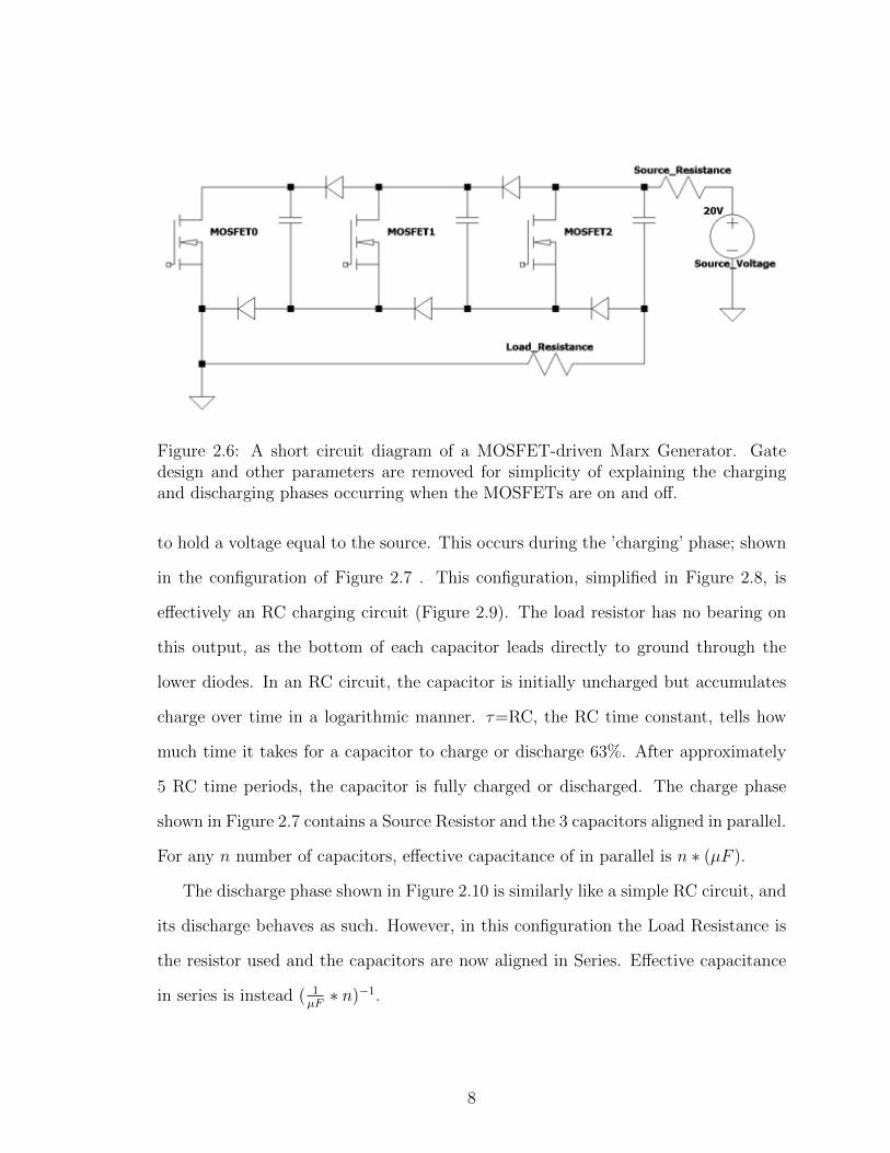
Figure 2.6: A short circuit diagram of a MOSFET-driven Marx Generator. Gatedesign and other parameters are removed for simplicity of explaining the chargingand discharging phases occurring when the MOSFETs are on and off.
to hold a voltage equal to the source. This occurs during the ’charging’ phase; shown
in the configuration of Figure 2.7 . This configuration, simplified in Figure 2.8, is
effectively an RC charging circuit (Figure 2.9). The load resistor has no bearing on
this output, as the bottom of each capacitor leads directly to ground through the
lower diodes. In an RC circuit, the capacitor is initially uncharged but accumulates
charge over time in a logarithmic manner. τ=RC, the RC time constant, tells how
much time it takes for a capacitor to charge or discharge 63%. After approximately
5 RC time periods, the capacitor is fully charged or discharged. The charge phase
shown in Figure 2.7 contains a Source Resistor and the 3 capacitors aligned in parallel.
For any n number of capacitors, effective capacitance of in parallel is n ∗ (µF ).
The discharge phase shown in Figure 2.10 is similarly like a simple RC circuit, and
its discharge behaves as such. However, in this configuration the Load Resistance is
the resistor used and the capacitors are now aligned in Series. Effective capacitance
in series is instead ( 1µF
∗ n)−1.
8

Figure 2.7: The charging phase of Figure 2.6. MOSFETs are off, and don’t conductcurrent.
Figure 2.8: The effective circuit presented in Figure2.7. Capacitors in parallel produce equivalentcapacitance of their sum.
Figure 2.9: The simplest form ofan RC circuit, reflective of Figure2.8.
Because the charge and discharge phases are dissimilar in using parallel capacitors
vs series capacitors, there exists a significant difference between their RC times.
Consider now the load resistance and source resistance to be equal (at 50kohm),
and a setup of 10 x 0.047µF capacitors.
During the charging phase, effective capacitance would be 0.47µF for a time
constant of 0.47 ∗ 10−6 ∗ R = 0.0235 seconds, suggesting a period of approximately
0.1175 seconds. During discharge, effective capacitance is 4.7nF for a time constant
9
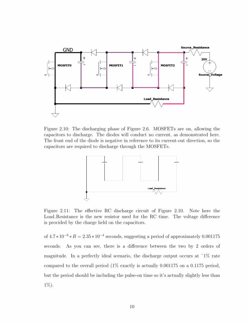
Figure 2.10: The discharging phase of Figure 2.6. MOSFETs are on, allowing thecapacitors to discharge. The diodes will conduct no current, as demonstrated here.The front end of the diode is negative in reference to its current-out direction, so thecapacitors are required to discharge through the MOSFETs.
Figure 2.11: The effective RC discharge circuit of Figure 2.10. Note here theLoad Resistance is the new resistor used for the RC time. The voltage differenceis provided by the charge held on the capacitors.
of 4.7∗ 10−9 ∗R = 2.35∗ 10−4 seconds, suggesting a period of approximately 0.001175
seconds. As you can see, there is a difference between the two by 2 orders of
magnitude. In a perfectly ideal scenario, the discharge output occurs at ˜1% rate
compared to the overall period (1% exactly is actually 0.001175 on a 0.1175 period,
but the period should be including the pulse-on time so it’s actually slightly less than
1%).
10

Figure 2.12: Charging and discharging graphs of an RC circuit. As shown here, τ isthe time needed to discharge [1 − 1
e]% of the charge on the capacitor.
2.3 Simulation Software
The production of this generator consisted of multiple trials in which a circuit was
considered, simulated, then tested in-person to verify the results of the simulation.
This is absolutely necessary when working with high voltages; not only for the
integrity of our circuit parts but also for the safety of the experimenter and the
health of the measuring devices.
There are many circuit simulators available, both proprietary and open-source.
SPICE (Simulation Program with Integrated Circuit Emphasis) is the progenitor of
all circuit simulators, releasing almost five decades ago. Several of the simulating
software still used today are variants on the SPICE code, to include the proprietary
software OrCAD, otherwise known as PSpice.
At first, we started using the built-in circuit simulation within Autodesk’s Fusion
360, which runs of Autodesk EAGLE, and NGSpice modeling software. We switched
to using LTSpice, an open-source SPICE simulation software with a built-in library
of both real parts to model with and a greater range of control at high frequency
regimes. This has made the simulations more accurate with real testing, and its
transient analysis allows us to work with far smaller time steps. The only limitation
now is that not all parameters the N-channel MOSFET uses are listed on the data
11
sheets for our parts. What has been included on the data sheet is accounted for in
the .model parameters.
2.4 Lab equipment
Our high voltage supply is an Hewlett-Packard DC power supply, model 6516A. It is
rated for a maximum output of 3kV and a maximum amperage of 6mA. In testing,
a maximum of 7.8mA was reached. However, both current values are quite low, and
result in longer recharge time for our pulse generator. Current is in the units of charge
over time, and thus for our capacitors to reach a certain charged state, lower values
of current will take longer for them to reach this state.
The Oscilloscope used is a Rohde & Schwarz HMO1202 Series. Its inputs are rated
for 200V for 1x probes. In testing, probes rated for high-voltage testing could not
match the frequency with which our pulses were occurring. As such, for high-voltage
outputs we continued with 1x to 10x probes, and simply used a voltage divider to
stay under the 200V limit of the oscilloscope, along with the 600V limit of the probes
on their 10x setting.
12

Chapter 3
Experimental Findings
The Marx Generator from the papers we originally referenced [9] [8] function
as demonstrated in Figure 2.2.
When testing this schematic, a number of issues were encountered. While our
MOSFETs can handle the high voltages maintained between the drain and source,
the voltage between its Gate and Source is still regulated to be ±20V. If this ±20V is
exceeded, the component will short and completely break. This is fine if the MOSFET
is acting as a simple transistor switch with the source outputting to ground, but each
of our MOSFET sources will be dropped to several kV below ground.
How the gates are connected up in [8] is clear, however the assembly produced
works in a much lower voltage regime. In addition, the paper entirely uses simulation
software (Multisim) to demonstrate the output. Experience with simulating these
MOSFETs indicates that often the simulated VGS exceeding this range does not result
in a ‘break’ of the part. As demonstrated in Figure 3.1, LTSpice allows the VGS to
rise to greater than 400V, but still operates as normal. As such, [8] is not a reliable
source for a gate driver for our purpose. Reference [9] utilizes a Marx Generator for
high negative voltage, but unfortunately the components making up the gate driver
in [9] are unclear and unlisted.
A major effort in this project has been to overcome the need for a gate that,
13
when turned on, will follow the source voltage in its immediate drop to high negative
voltage, while maintaining the ”on” state needed in the MOSFET during the discharge
phase.
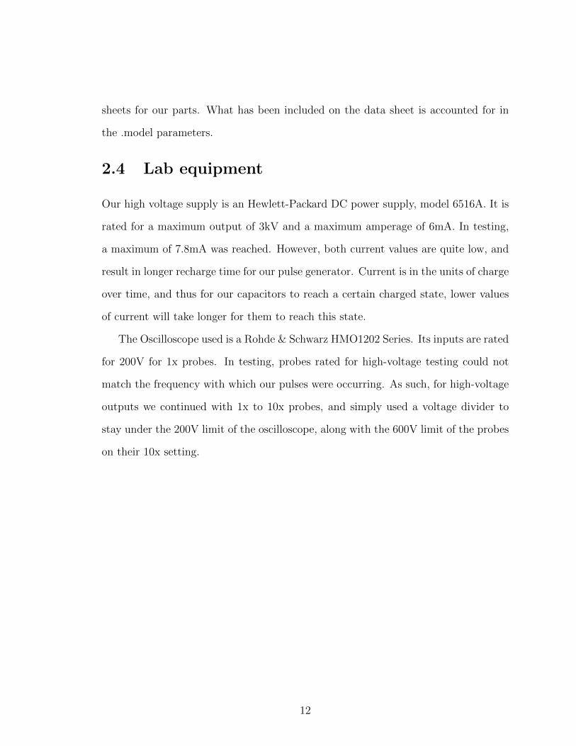
Figure 3.1: Simulation output of voltage/time for the gate and source voltages onthe third stage of a three-stage Marx Generator circuit (1kV input voltage). Blue isGate pin, Red is Source pin. Demonstrates that despite the MOSFETs having a hardbreaking point at VGS > 20V, the simulation accepts VGS exceeding at most 800V!Simulations may not prove sufficient to demonstrate potential use, especially not in[8].
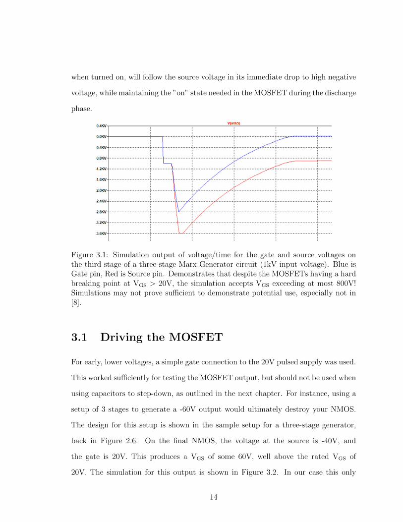
3.1 Driving the MOSFET
For early, lower voltages, a simple gate connection to the 20V pulsed supply was used.
This worked sufficiently for testing the MOSFET output, but should not be used when
using capacitors to step-down, as outlined in the next chapter. For instance, using a
setup of 3 stages to generate a -60V output would ultimately destroy your NMOS.
The design for this setup is shown in the sample setup for a three-stage generator,
back in Figure 2.6. On the final NMOS, the voltage at the source is -40V, and
the gate is 20V. This produces a VGS of some 60V, well above the rated VGS of
20V. The simulation for this output is shown in Figure 3.2. In our case this only
14

occurs during a very short time scale, after which the difference quickly recovers to
reasonable values. Additionally, due to the internal capacitance of the MOSFET
there is an additional delay built-in to the VGS. In our testing of this setup, the third
MOSFET would eventually break but could go several pulses without impact, due to
these discrepancies. Even working at smaller time scales, the VGS specifications need
to be appropriately met.
Figure 3.2: Simulated output for a pulse from the 3 stage pulse generator at a 20Vinput, graphed in voltage over time. Blue is the final MOSFET’s gate; red is it’ssource. The VGS is exceeded during this pulse.
3.1.1 Floating Gate Voltage
The next design attempted to keep the gate in-line with the source by connecting them
with capacitors with more Farads than the internal capacitance within the MOSFETs
(Figure 3.3). During the charging phase, the gate capacitors will be grounded out and
hold a 0V potential difference. Upon receiving a 20V gate input, the generator enters
into its discharge phase, and the sources of the later MOSFETs enter a high negative
voltage regime. The capacitors at each gate will discharge over a set amount of time
to approach the new voltage difference. At the instantaneous point of switching,
15
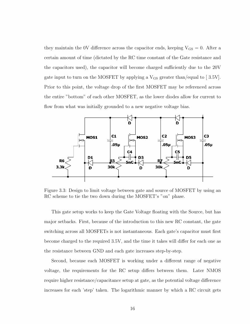
they maintain the 0V difference across the capacitor ends, keeping VGS = 0. After a
certain amount of time (dictated by the RC time constant of the Gate resistance and
the capacitors used), the capacitor will become charged sufficiently due to the 20V
gate input to turn on the MOSFET by applying a VGS greater than/equal to [ 3.5V].
Prior to this point, the voltage drop of the first MOSFET may be referenced across
the entire ”bottom” of each other MOSFET, as the lower diodes allow for current to
flow from what was initially grounded to a new negative voltage bias.
Figure 3.3: Design to limit voltage between gate and source of MOSFET by using anRC scheme to tie the two down during the MOSFET’s ”on” phase.
This gate setup works to keep the Gate Voltage floating with the Source, but has
major setbacks. First, because of the introduction to this new RC constant, the gate
switching across all MOSFETs is not instantaneous. Each gate’s capacitor must first
become charged to the required 3.5V, and the time it takes will differ for each one as
the resistance between GND and each gate increases step-by-step.
Second, because each MOSFET is working under a different range of negative
voltage, the requirements for the RC setup differs between them. Later NMOS
require higher resistance/capacitance setup at gate, as the potential voltage difference
increases for each ’step’ taken. The logarithmic manner by which a RC circuit gets
16

charged is the same for all gates, but takes longer for later MOSFETs because they
have higher RC values at their gate. This difference in gate charging time further
contributes to the loss of efficiency.
Ultimately, this solution doesn’t completely remove the potential for breaking
down the gate at low voltages. Because of the delays caused by the prior two points,
the time it takes to fully switch the system is much longer. This length of time
lets the gate capacitors become charged as the Source gets referenced further towards
ground. Consider the 5 stage setup in Figure 3.4. At the final MOSFET, the effective
RC configuration at the gate is between -200V and GND. The capacitor at this
MOSFET’s gate will charge up due to this potential difference. Given enough time,
this capacitor (which is effectuating VGS) would reach 200V and would break the
part. This is shown in the voltage output curve, which demonstrates the growing
voltage difference between the two. A workaround to this flaw is to further increase
the time needed to charge up to this value by increasing the R and C values at the
gates. However, this creates further issues with the time at which turn-on happens
for each MOSFET, and results in significant efficiency loss in the voltage output.
Figure 3.4: 5 stages utilizing the RC gate configuration. Input voltage is 50V,resulting in an ideal output of 250V.
17

Figure 3.5: Simulated voltage vs time output of Figure 3.4 at the final MOSFET.Gate shown in red, Source in blue. As you can see, over time the difference betweenthe two increases, until the source becomes referenced at GND. Steps shown are dueto the offsets for each step turning off caused by efficiency loss within the RC gatesystem.
3.1.2 Zener Gate Voltage
This leads us into our next design decision. Considering that the error occurs once
the gates have already passed the turn-on time, and are simply reaching VGS values
higher than 20V, a zener diode was considered. Zener diodes operate like normal
diodes in that they allow current to pass through in a certain direction. In technical
drawings, the arrow’s direction is the direction in which current passes, just like a
normal diode. The key use of a zener is that when the backwards voltage across is
reaches a certain value (detailed in its specs sheet), it passes current in a backwards
operation as well. By using zener diodes that are rated for 20V or less, we can set
a hard cap on the VGS. Whenever the Source voltage would be less than the Gate
by more than 20V, the zener allows a back-current from the Source into the gate to
lower the gate further. Before, additional capacitance was used to tether down the
Gate voltage to the source. Now, this is being done with the Zener, and produces an
18

effect that is much more efficient and never exceeds the VGS rating of the MOSFETs.
The Zener Diodes used were model 2M17Z R0 from Taiwan Semiconductor, with
a 17V zener voltage and a 107mA zener current.
Adjusting Figure 3.4 for this new Zener-driven discharge, the new circuit setup
for 5 stages is shown in Figure 3.6. The output is shown in Figure 3.7, which shows
a much cleaner curve and a VGS that never exceeds 20V along its entire pulse.
Figure 3.6: New gate configuration of the 5 stage setup, using zener diodes todischarge at the gate
3.1.3 Self-Driving MOSFETs Using Zeners
Finally, there is one more adjustment to the Gate setup at the MOSFETs that further
improves efficiency AND simplifies the response.
With this setup, the initial leftmost MOSFET is pulsed on as usual, with the Gate
receiving 20V to turn on and the Source always remaining grounded. No VGS issues
have ever occurred at this location.
Upon the initial MOSFET (MOSFET 0) turning on grounding the top of its
respective capacitor, the source of the MOSFET 1 becomes referenced to -1kV/-3kV
etc. At an instantaneous point, the internal capacitance within the MOSFET brings
the Gate down to -1kV/-3kV along with it, keeping VGS at 0 for the instantaneous
time of MOSFET 0 switching on. Barring the zener diode, the gate is now a simple
19
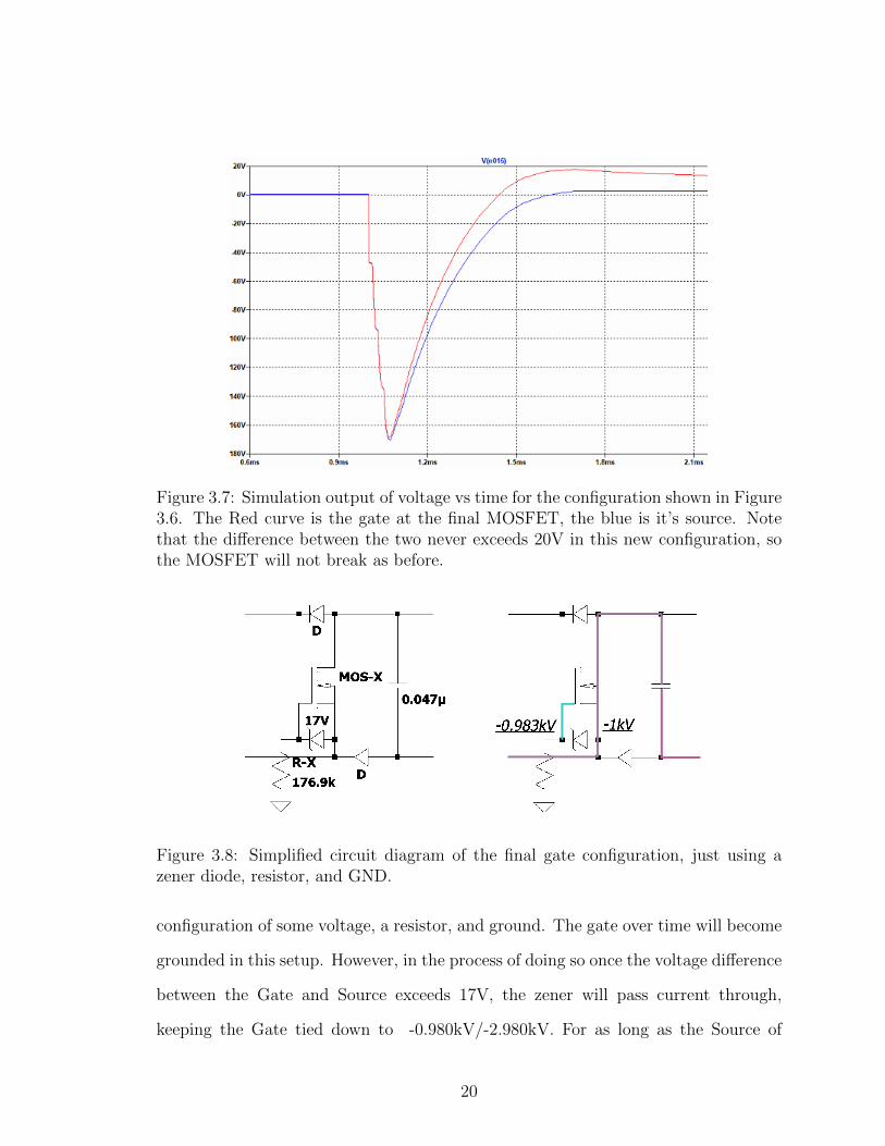
Figure 3.7: Simulation output of voltage vs time for the configuration shown in Figure3.6. The Red curve is the gate at the final MOSFET, the blue is it’s source. Notethat the difference between the two never exceeds 20V in this new configuration, sothe MOSFET will not break as before.
Figure 3.8: Simplified circuit diagram of the final gate configuration, just using azener diode, resistor, and GND.
configuration of some voltage, a resistor, and ground. The gate over time will become
grounded in this setup. However, in the process of doing so once the voltage difference
between the Gate and Source exceeds 17V, the zener will pass current through,
keeping the Gate tied down to -0.980kV/-2.980kV. For as long as the Source of
20
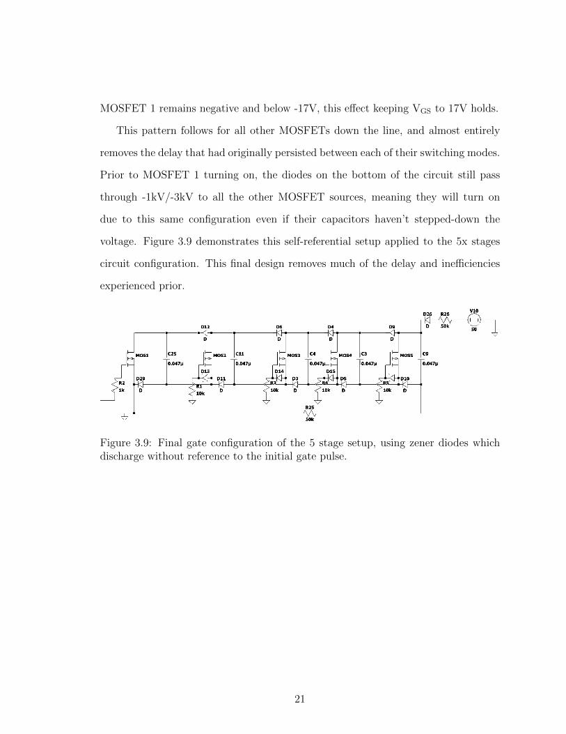
MOSFET 1 remains negative and below -17V, this effect keeping VGS to 17V holds.
This pattern follows for all other MOSFETs down the line, and almost entirely
removes the delay that had originally persisted between each of their switching modes.
Prior to MOSFET 1 turning on, the diodes on the bottom of the circuit still pass
through -1kV/-3kV to all the other MOSFET sources, meaning they will turn on
due to this same configuration even if their capacitors haven’t stepped-down the
voltage. Figure 3.9 demonstrates this self-referential setup applied to the 5x stages
circuit configuration. This final design removes much of the delay and inefficiencies
experienced prior.
Figure 3.9: Final gate configuration of the 5 stage setup, using zener diodes whichdischarge without reference to the initial gate pulse.
21
Chapter 4
Results
4.1 Circuit Testing
The first in-person testing was the 3-stage Marx generator with 20V input. Probing
the voltage at the load resistor nets us Figure 4.2, successfully showing the buildup of
charge for a more negative voltage output. This matches up well with the simulation
output. Running this setup for a prolonged period will eventually short out the final
MOSFET in the chain due to the aforementioned exceeding of VGS.
After the first change at the gate, adding an RC component for the gate-source
voltage, another test was conducted for a new 3-stage generator with a 100V input.
The output shown in Figure 4.3 shows the VGS staying within the MOSFET’s rated
limits.
For further changes to the circuit configuration, the simulation needed to with
certainty demonstrate a VGS within the acceptable range. Thus, in person testing
resumed after the successful demonstration of the zener-type gate configuration. At
this point, the 5 stage pulse generator was ready to be tested. Figures 4.4 and 4.5
showcase the outputs of the circuit from Figure 3.6, outputting 5x100V and 5x500V
at the load resistor respectively. Values exceeding -600V must be parsed through a
22
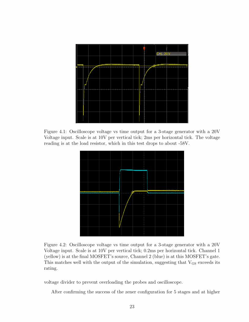
Figure 4.1: Oscilloscope voltage vs time output for a 3-stage generator with a 20VVoltage input. Scale is at 10V per vertical tick; 2ms per horizontal tick. The voltagereading is at the load resistor, which in this test drops to about -58V.
Figure 4.2: Oscilloscope voltage vs time output for a 3-stage generator with a 20VVoltage input. Scale is at 10V per vertical tick; 0.2ms per horizontal tick. Channel 1(yellow) is at the final MOSFET’s source, Channel 2 (blue) is at this MOSFET’s gate.This matches well with the output of the simulation, suggesting that VGS exceeds itsrating.
voltage divider to prevent overloading the probes and oscilloscope.
After confirming the success of the zener configuration for 5 stages and at higher
23

Figure 4.3: Oscilloscope output for a 3-stage generator with a 100V Voltage input.This reading compares the source and gate voltages at the third MOSFET, the oneprior to the load resistor. Channel 1 (yellow) is the voltage at its source, Channel 2(blue) is the voltage at its gate; tick marks are 50V (vertical) and 1ms (horizontal).What is shown here is that the source successfully brings the gate lower as it drops,reducing the VGS that would otherwise break the component.
Figure 4.4: Oscilloscope output; voltage (100V/tick) vs time (100µs/tick); CH1yellow:input pulse of 20V; CH2blue: output pulse, reaching -476V from a 100V input across5 stages.
24

Figure 4.5: Oscilloscope output; voltage (100V/tick) vs time (100µs/tick); CH1yellow:input pulse of 20V; CH2blue: output pulse, reaching approximately -2500V from a500V input across 5 stages.
voltages than we had yet tested, a 10x stage circuit was built. This also required using
diodes rated higher than we had previously used; each diode needs to be rated for at
least the input voltage, as this is the voltage difference across each stage. Outputs
for the 10 stages go through a voltage divider which reduces the output by a factor
of 1/53. Table 4.1 lists the output from this test.
Results stopped after the source resistor fried, which was used to maintain a
voltage difference between the input voltage and the final capacitor. The final output
graph taken is shown in Figure 4.6 At the time, this was a 220kΩ resistor. The
replacement resistor used was 2.2MΩ, and allowed us to continue increasing our input
voltage. Table 4.2 shows the rest of the measurements, after making this replacement.
Upon reaching 20kV for our output, the load resistor completely snapped apart
due to the power being put across it. Figure 4.7 is the last oscilloscope reading before
the load resistor failed.
25
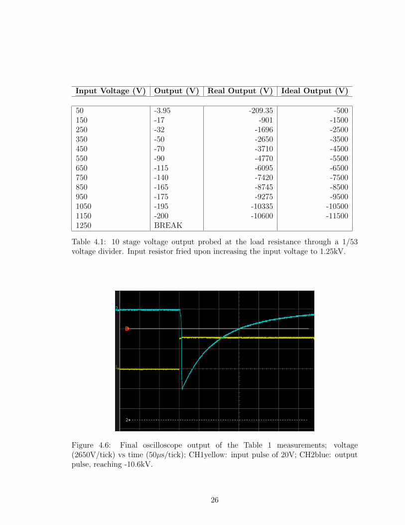
Input Voltage (V) Output (V) Real Output (V) Ideal Output (V)
50 -3.95 -209.35 -500150 -17 -901 -1500250 -32 -1696 -2500350 -50 -2650 -3500450 -70 -3710 -4500550 -90 -4770 -5500650 -115 -6095 -6500750 -140 -7420 -7500850 -165 -8745 -8500950 -175 -9275 -95001050 -195 -10335 -105001150 -200 -10600 -115001250 BREAK
Table 4.1: 10 stage voltage output probed at the load resistance through a 1/53voltage divider. Input resistor fried upon increasing the input voltage to 1.25kV.
Figure 4.6: Final oscilloscope output of the Table 1 measurements; voltage(2650V/tick) vs time (50µs/tick); CH1yellow: input pulse of 20V; CH2blue: outputpulse, reaching -10.6kV.
26

Input Voltage (V) Output (V) Real Output (V) Ideal Output (V)
1050 -175 -9275 -105001150 -200 -10600 -115001250 -220 -11660 -125001350 -230 -12190 -135001450 -240 -12720 -145001550 -290 -15370 -155001650 -330 -17490 -165001750 -350 -18550 -175001850 -375 -19875 -185001950 BREAK
Table 4.2: 10 stage voltage output probed at the load resistance through a 1/53voltage divider. Load resistance broke upon increasing the input voltage to 1.95kV.Real outputs seem to exceed the ideal outputs; this may be due to pushing thelimitations of the resistors used, causing a probe mis-read.
Figure 4.7: Final oscilloscope output of the Table 2 measurements; voltage(5300V/tick) vs time (5µs/tick); CH1yellow: input pulse of 20V; CH2blue: outputpulse, reaching -19.8kV.
27

Chapter 5
Conclusion
In this experiment, we sought to produce a generator that output a pulse
conducive to the requirements for Plasma-Immersion Ion Implantation. It needed
to be pulsed for a controlled amount of time and supply a high negative voltage. To
do this, we devised a pulse-controlled Marx Generator that used MOSFETs to act as
the switching mechanism. Our final output was a -20kV pulse that could hold 20µs
before a voltage loss of 75%. As discussed in Chapter 2.1, this is within the ballpark
of the output necessary for implantation.
There are limitations on this output. First, the final pulse output was set at 1Hz.
For a 20µs pulse, a 1% duty cycle would suggest 500Hz would be your maximum
pulse frequency. In our case, the main limiter is our high voltage power supply only
supplying at most 7mA. This severely increases the recharge time on the capacitors,
even if all other components are rated for far higher amperage.
The amperage of the system’s output is another limitation. The source resistance
used of 50kΩ may be an overestimate for the conditions of the plasma, but even so
the current MOSFETs used are only rated for 0.25A. While the process of PIII will
still occur under this lower amperage, the amount of implanting as a factor of time
gets severely cut. This is the case with the frequency limit as well. Both of these
conditions mean this generator would output at a very slow rate.
28

As for the loss of voltage during the pulse, this can be remediated by using higher
capacitance on each step to increase the RC discharge time constant. This is especially
necessary if the effective load resistance is much lower than expected. As discussed in
Chapter 2.2.3, the charge and discharge rates are determined both by the capacitors in
series/parallel and their respective resistances. In regards to this, higher capacitance
may increase the discharge time but would necessarily require a longer recharge time
as well. The net effect of which more severely impacts the recharge time, as the time
between charge and recharge differs by a factor of n2 depending on the number of
steps.
In our experiment, the source resistance was absolutely necessary to hold the
voltage difference between the source and the final segment of the Marx Generator,
which would be highly negative. A useful alternative would be to reduce the source
resistance to improve recharge time, and put a large inductor in series with it. An
inductor’s utility in preventing change of current is perfect holding back current from
the source high voltage during our small pulses, and wouldn’t impede the current
during the bulk of the recharge phase. This addition would make both using higher
capacitance and supplying higher current much more feasible.
29

Bibliography
[1] J.Brutscher, R. Gunzel, W. Moller. Plasma immersion ion implantation using
pulsed plasma with d.c. and pulsed high voltages. Surface and Coatings
Technology. [Volume 93 PP 197-202]. (1997);
https://doi.org/10.1016/S0257-8972(97)00044-3
[2] Kyoung-Jae Chung, Soon-Wook Jung, Jae-Myung Choe, Gon-Ho Kim, and Y.
S. Hwang , ”Self-consistent circuit model for plasma source ion implantation”,
Review of Scientific Instruments 79, 02C502 (2008)
https://doi.org/10.1063/1.2816792
[3] J. R. Conrad, J. L. Radtke, R. A. Dodd, Frank J. Worzala, and Ngoc C. Tran.
Plasma source ion-implantation technique for surface modification of materials.
Journal of Applied Physics 62, 4591 (1987); https://doi.org/10.1063/1.339055
bibitemmichaelMichael A. Liberman and Allan J. Lichtenberg, Principles of
plasma discharges and material processing, Ed. New York: John Wiley and
Sons, 1994.
[4] Wu, Lingling, ”Surface processing by RFI PECVD and RFI PSII” (2000).
Dissertations, Theses, and Masters Projects. Paper 1539623997.
[5] Paolo Nenzi, Holger Vogt. Ngspice Users Manual Version 26 (2014) page 131.
30

[6] M. C. Salvadori, F. S. Teixeira, ... and I. G. Brown , ”A high voltage pulse
power supply for metal plasma immersion ion implantation and deposition”,
Review of Scientific Instruments 81, 124703 (2010)
https://doi.org/10.1063/1.3518969
[7] Schwirzke F. (1986) Plasma Jets Emitted by Unipolar Arcing from Spherical
Laser Targets. In: Hora H., Miley G.H. (eds) Laser Interaction and Related
Plasma Phenomena. Springer, Boston, MA.
https://doi.org/10.1007/978-1-4615-7335-7 62
[8] A.Sojitra, H.Rana,... S.De. 5 Stage, 50 V, 500 Hz, 50 µs MOSFET Based
Design Of Unipolar Pulse Power Marx Generator. IOSR Journal of
Engineering [Volume 9, PP 65-70]. (2018)
[9] Tokuchi, A., Jiang, W., Takayama, K., Arai, T., Kawakubo, T., & Adachi, T.
(2012). Development of MOS-FET based Marx generator with self-proved gate
power (NIFS-PROC–90). Hotta, Eiki, & Ozaki, Tetsuo (Eds.). Japan
[10] Marx Generator [Schematic diagram of a Marx generator]. (2009, November
1). Retrieved from https://en.wikipedia.org/wiki/Marx generator#/media/
File:Marx Generator.svg
[11] IXYS ”High Voltage Power MOSFET”, IXTF1N450, 2013 IXYS,
http://ixapps.ixys.com/DataSheet/DS100501D(IXTF1N450).pdf
[12] IXYS ”High Voltage Power MOSFET”, IXTH04N300P3HV, 2014 IXYS,
http://ixapps.ixys.com/DataSheet/DS100638(IXTH04N300P3HV).pdf
31