Embed Size (px)
Citation preview

Martin Pospíšilík
Introductionto ElectromagneticCompatibilityfor ElectronicEngineers … and not only for them
PDF kniha


Introduction to Electromagnetic Compatibility for Electronic Engineers
… and not only for them
Martin Pospíšilík
Zlín, 2019

KATALOGIZACE V KNIZE - NÁRODNÍ KNIHOVNA ČR
Pospíšilík, Martin Introduction to electromagnetic compatibility for electronic engineers : ...and not only for them / Martin Pospíšilík. -- First edition. -- Zlín : Tomas Bata University in Zlín, 2019. -- 1 online zdroj Obsahuje bibliografii
ISBN 978-80-7454-876-5 (online ; pdf)
* 621.37-021.29 * (048.8) – elektromagnetická kompatibilita
– monografie
621.3 - Elektrotechnika [19]
Introduction to Electromagnetic Compatibility for Electronic Engineers … and not only for them
Author: Ing. Martin Pospíšilík, Ph.D.
Expert reviewers: Ing. Pavel Tobola, CSc. doc. Ing. Kamil Madáč, CSc.
Language proofreading: Mgr. Klára Pospíšilíková Lecturers: doc. RNDr. Vojtěch Křesálek, CSc.
doc. Mgr. Milan Adámek, Ph.D.
978-80-7454-876-5
© Copyright Tomas Bata University in Zlín, 2019
© Copyright Martin Pospíšilík, 2019
https://doi.org/ 10.7441/978-80-7454-876-5

3
1 CONTENTS
1 Contents........................................................................................ 3
2 Foreword ...................................................................................... 6
3 Brief introduction to electromagnetism ........................................ 7
3.1 Electrical Charge ...................................................................... 7
3.2 Electrostatic field ..................................................................... 8
3.3 Electric potential and voltage .................................................. 9
3.4 Electric current ....................................................................... 11 3.4.1 How the electric current is generated ............................... 12 3.4.2 Effects of electric current .................................................. 14 3.4.3 Current density .................................................................. 15
3.5 Magnetic field ........................................................................ 16 3.5.1 Magnetic field around conductor ...................................... 18
3.6 Quasi stationary electromagnetic field .................................. 19 3.6.1 Faraday’s law of induction................................................. 20 3.6.2 Displacement current ........................................................ 21
3.7 Electromagnetic waves .......................................................... 23 3.7.1 Electromagnetic waves in non-conductive isotropic environment ................................................................................... 23
4 Electromagnetic compatibility ..................................................... 29
4.1 Sub-disciplines ........................................................................ 30
4.2 Electromagnetic interference................................................. 32
4.3 Electromagnetic susceptibility ............................................... 33
4.4 Limits and Functional criteria ................................................ 34
4.5 Standards and legislation ...................................................... 36 4.5.1 National and International Standardization bodies .......... 37 4.5.2 Legally defined requirements ............................................ 39

4
4.5.3 Hierarchy of standards ...................................................... 42 4.5.4 Military and other special standards ................................. 44
5 Conditions in EMC Labs ............................................................... 46
5.1 Open area test site ................................................................. 46
5.2 Electromagnetically shielded rooms ...................................... 49
5.3 Anechoic and semi anechoic rooms ....................................... 52
5.4 Electromagnetic reverberation rooms ................................... 59
5.5 Attenuation of the measurement site .................................... 59
5.6 EMC labs instrumentation ...................................................... 61 5.6.1 Interference meters ........................................................... 61 5.6.2 Interference generators ..................................................... 68 5.6.3 Antennas ............................................................................ 73 5.6.4 Near field probes ............................................................... 80 5.6.5 Tools for measurement of conducted interferences ......... 81
6 Tests on electromagnetic interferences ...................................... 89
6.1 Radiated interferences of commercial devices ....................... 89
6.2 Conducted emissions of commercial devices ......................... 92
6.3 EMI tests on other than commercial devices ......................... 96
7 Tests on electromagnetic susceptibility ...................................... 97
7.1 Electrostatic discharge immunity test .................................... 97
7.2 Radiated radio-frequency electromagnetic field .................. 100
7.3 Electrical fast transients ....................................................... 102
7.4 Surge wave ........................................................................... 105
7.5 Conducted radio-frequency interferences ............................ 106
7.6 Power supply errors ............................................................. 107 7.6.1 Voltage dips ..................................................................... 107 7.6.2 Short interruption ............................................................ 107

5
7.6.3 Voltage sags ..................................................................... 107 7.6.4 Instrumentation .............................................................. 107
8 References ................................................................................ 108
9 Abbreviations ............................................................................ 109

6
2 FOREWORD
During his academic and engineering experience in the field of electronics and electromagnetic compatibility, the author of this book has encountered similar and frequently recurring problems, as well as questions from students and circuit designers. Therefore he decided to prepare this brief text as a guide for those interested in electromagnetic compatibility, covering the issues from the design of electronic devices up to their certification in accordance with laws. The aim was to explain the most important principles without exhaustive definitions, but without prejudice to the correctness of the interpretation at the same time. The interpretation of the issues is complemented by personal experience of the author obtained in the field of EMC measurements.
Inside this book, the reader will find a very brief introduction to the theory of electromagnetic field, which is necessary to understand the main EMC issues. Subsequently, there is a chapter devoted to general description of the EMC issues. The author’s aim consisted in an attempt to provide such description that can be understood by specialists who do not make their livings by designing electronic circuits as such. This includes, for example, project managers, technical science teachers, technical business representatives et cetera. This general information is followed by another non-technical part that provides a description on general law requirements concerning the electromagnetic compatibility. This issue cannot be omitted as applicable laws in every country in the world require the electronic devices to fulfil minimum requirements on their interference limits, safety of operation and reliability. Afterwards the “technician’s area” begins. The next chapter provide description on the instrumentation applied in EMC laboratories and the most frequent tests. With each of the tests, the relevant standards, laboratory configuration, typical results and the author’s experience are mentioned.
The author hopes that not only the technicians and circuit designers, but also his academic colleagues will find enriching and inspiring pieces of information within the framework of this text.

7
3 BRIEF INTRODUCTION TO ELECTROMAGNETISM
Since the beginning of 19th century, leading world scientists tried to clarify why electrically charged particles can act by force without touching each other. In 1873, James Clerk Maxwell in his work “A treatise on electricity and magnetism” stated the following ideas:
1. Particles interact with each other by force only because they exist.2. Electromagnetic field is the medium that ensures mutual contact of the
particles.3. The behaviour of the electromagnetic field can be described by methods
proposed by Michael Faraday.
Obviously, modern physics provides much more complex insight into the phenomenon of electromagnetic field. However, for the purposes of this book, the 19th century model seems to be sufficiently clear. In this chapter, the reader will find a very brief description on what electromagnetism is and what quantities are recognized and evaluated. Readers with knowledge of this subject can skip to the following chapter.
3.1 ELECTRICAL CHARGE All matter in the nature consists of positively and negatively charged particles which compensate each other and therefore most objects appear to be electrically neutral. However, under some circumstances that are described below, the particles can be isolated. In such a case, positively or negatively charged object is obtained.
The smallest amount of charge is held by either electron or proton. By convention set by Benjamin Franklin, the electrons are considered as negatively charged while the protons are considered as positively charged. In both cases, the smallest amount of charge is usually noted as “q” and its value can be expressed in Coulombs:
𝑞𝑞 = 1.162 ∙ 10−19 [𝐶𝐶] (1)
This means that the amount of charge is always quantized and the charge of any object can be calculated according to the number of uncompensated positive or negative particles on its surface. The total charge can then be expressed as follows:
𝑄𝑄 = 𝑛𝑛𝑞𝑞 [𝐶𝐶] (2)
https://doi.org/ 10.7441/978-80-7454-876-5
https://doi.org/10.7441/978-80-7454-876-5_1

8
Where: n is the number of the charged particles q.
3.2 ELECTROSTATIC FIELD In 1785, Charles Augustin de Coulomb recognized by experiment that two charged particles interact with each other by force. If both particles are charged with the same polarity, they repel each other, but if their polarity is different, they attract each other. The force acting between the particles can be expressed as follows:
𝐹𝐹 =1
4𝜋𝜋𝜀𝜀0𝜀𝜀∙𝑞𝑞1𝑞𝑞2𝑟𝑟2 [𝑁𝑁] (3)
Where: q1, q2 are the charges of the particles in Coulombs, r is the distance between the particles, ε0 is permittivity of vacuum, 𝜀𝜀0 = 8.854 [𝐹𝐹 ∙ 𝑚𝑚−1] , ε is relative permittivity of the material in which the interaction occurs.
The equation (3) is known as Coulomb’s law and has the following consequence: around each charged particle there exists a field that interacts with other charged particles. If the charged particle does not move and the amount of its charge does not change, the field around the particle is called electrostatic. Generally, the field generated by the charged particles is called “winged”, because it protrudes from one point and spreads to infinity. Michael Faraday’s field lines can be used to visualise this.
+
Figure 1. If not affected by other charges around, the field lines start in the middle of the positive charge and spread to infinity.

9
Regarding the electric field, one of the basic quantities is its intensity. It is defined as a force that acts on the charge Q which is as high as 1 Coulomb.
𝐸𝐸 =𝐹𝐹𝑄𝑄 [𝑁𝑁 ∙ 𝐶𝐶−1] (4)
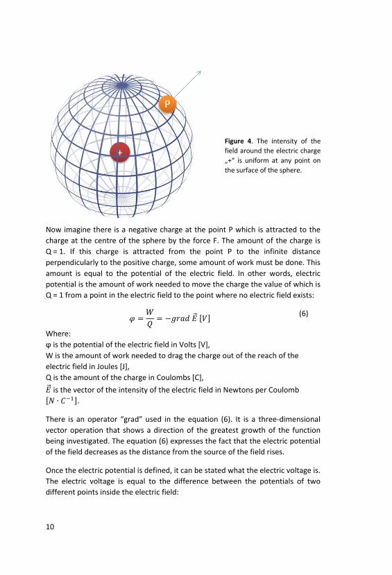
3.3 ELECTRIC POTENTIAL AND VOLTAGE Imagine there is only a point charge inside an infinite free space. Its electric field is uniformly distributed around. Therefore, if a sphere is made around this charge, the intensity of electrical field will be constant at all points of its surface (see Fig. 4). For example, at the point P, which lies on the surface of the sphere, the intensity of the electric field can be expressed as follows:
𝐹𝐹 =1
4𝜋𝜋𝜀𝜀0𝜀𝜀∙𝑄𝑄𝑟𝑟2 [𝑁𝑁] (5)
Where: Q is the charge in Coulombs, r is the radius of the sphere.
-
- +
Figure 2. If not affected by other charges around, the field lines finish in the middle of the negative, approaching from the infinity.
Figure 3. Positive and negative charges create a dipole. The field lines begin in the middle of the positive charge and finish in the middle of the negative one.
10
Now imagine there is a negative charge at the point P which is attracted to the charge at the centre of the sphere by the force F. The amount of the charge is Q = 1. If this charge is attracted from the point P to the infinite distance perpendicularly to the positive charge, some amount of work must be done. This amount is equal to the potential of the electric field. In other words, electric potential is the amount of work needed to move the charge the value of which is Q = 1 from a point in the electric field to the point where no electric field exists:
𝜑𝜑 =𝑊𝑊𝑄𝑄 = −𝑔𝑔𝑟𝑟𝑔𝑔𝑔𝑔 𝐸𝐸 [𝑉𝑉] (6)
Where: ϕ is the potential of the electric field in Volts [V], W is the amount of work needed to drag the charge out of the reach of the electric field in Joules [J], Q is the amount of the charge in Coulombs [C], 𝐸𝐸 is the vector of the intensity of the electric field in Newtons per Coulomb [𝑁𝑁 ∙ 𝐶𝐶−1].
There is an operator “grad” used in the equation (6). It is a three-dimensional vector operation that shows a direction of the greatest growth of the function being investigated. The equation (6) expresses the fact that the electric potential of the field decreases as the distance from the source of the field rises.
Once the electric potential is defined, it can be stated what the electric voltage is. The electric voltage is equal to the difference between the potentials of two different points inside the electric field:
Figure 4. The intensity of the field around the electric charge „+“ is uniform at any point on the surface of the sphere.

11
𝑈𝑈 = |𝜑𝜑2 − 𝜑𝜑1| [𝑉𝑉] (7)
Meaning of the expression (7) is described by the Figure 5. There are two points the electric potential of whose is ϕ1 and ϕ2. The difference between them can be expressed as electric voltage U. The red force lines express the vectors of the intensity of the electric field 𝐸𝐸 . In the text above, the intensity of the field was expressed in Newtons per Coulomb [𝑁𝑁 ∙ 𝐶𝐶−1]. The same meaning has the quantity Volts per meter [𝑉𝑉 ∙ 𝑚𝑚−1] , which is more likely to be used in electronics and physics.
3.4 ELECTRIC CURRENT In the subchapters above, static electric field was described. However, in electric circuits there is usually a need for motion of the charged particles as this is a way to transfer the energy. Once a charged particle is put into the electric field, when not firmly fixed in the structure of the material, it tends to move, being attracted by the electric force F (see equation (5)).
First of all, let us mention that from the “conductive” point of view, there is a distinction between two types of materials.
The first type is called dielectrics. These are the materials that contain all the charged particles fixed in the material structure, thus no electric current can be driven in them. When dielectrics are put into the electric field, they are polarized. That means that the atoms and/or molecules are positioned according to the direction of the external field, but cannot move as their atomic and/or molecular bonds are too strong. The electric field creates forces inside the material that are proportional to its intensity. When the electrical strength limit of such material is exceeded, ionization occurs. As a result, free electrons teared by the electric force
Figure 5. Difference of the potential between the two points is expressed as voltage in Volts [V].
+
ϕ1 ϕ2
U
12
out of the atoms start to move and the material starts to conduct the electric current. Usually, its conductivity increases rapidly. A typical example is the ionization of the air, resulting in lightning during thunderstorms.
Materials of the second type are called conductors. These materials contain electrons that are poorly bound to their crystal lattice and when electric field is applied to them, these electrons start to move immediately. As a result, electric current in the conductor occurs. The intensity of the electric current is expressed in Amperes [A] as an amount of charge Q that has flown through a cut of the wire in one second:
𝐼𝐼 =∆𝑄𝑄∆𝑡𝑡
[𝐴𝐴] (7)
Where: ΔQ is the change of the charge in Coulombs [C], Δt is the change of the time in seconds [s].
In these terms, the most important quantity to describe the ability of the conductor to conduct the electric current is the conductance G which is expressed in Siemens [S]. The conductor has a conductance of one Siemens just when there is a voltage of 1 Volt between its edges and the current flowing through it is as high as 1 Ampere:
𝐺𝐺 =𝐼𝐼𝑈𝑈
[𝑆𝑆] (8)
In practice it is more convenient to apply the inverted quantity which is called the electric resistance. It is expressed in Ohms [Ω] and is defined as follows:
𝑅𝑅 =𝑈𝑈𝐼𝐼 =
1𝐺𝐺
[Ω] (9)
Provided the electric current is constant in time, it is called stationary. When the current does not change its direction in time, it is called direct (DC). On the contrary, when the direction of the current alternates in time, it is called alternating (AC).
3.4.1 How the electric current is generated The electric current in the conductor can occur only when the following conditions are fulfilled:
13
1. The electric circuit must be closed (the charged particles (electrons) must have a chance to circulate).
2. There must be at least one point in the closed electric circuit in which there a force exists that makes the charged particles move.
The first point is probably obvious. If the circuit is not closed, the electric current may not flow through it. The second point says that there must be a source of energy that makes the electrons flow through the circuit. If there was only the stationary electric field, described in the subchapter 2.3, no stationary current would occur. The electrons would move to the positions relevant to the electrostatic forces inside the circuit and stop. A steady state would be reached and the current would disappear. Therefore, two basic kinds of elements of electrical circuits are distinguished:
• Sources that put the energy into the circuit, • Loads that consume this energy.
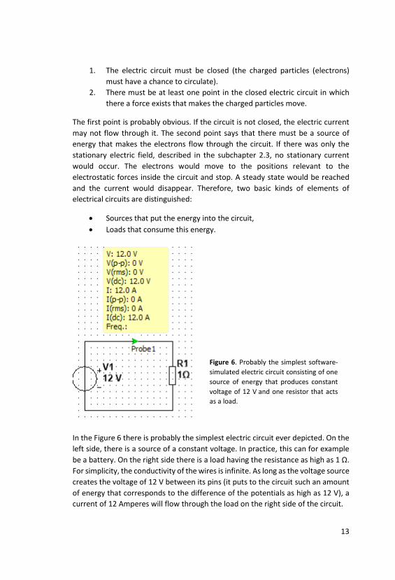
In the Figure 6 there is probably the simplest electric circuit ever depicted. On the left side, there is a source of a constant voltage. In practice, this can for example be a battery. On the right side there is a load having the resistance as high as 1 Ω. For simplicity, the conductivity of the wires is infinite. As long as the voltage source creates the voltage of 12 V between its pins (it puts to the circuit such an amount of energy that corresponds to the difference of the potentials as high as 12 V), a current of 12 Amperes will flow through the load on the right side of the circuit.
Figure 6. Probably the simplest software-simulated electric circuit consisting of one source of energy that produces constant voltage of 12 V and one resistor that acts as a load.

14
3.4.2 Effects of electric current Once the electric current flows through a conductor, two basic effects can be observed:
1. Heat generation. 2. Magnetic field generation.
The first phenomenon has been described by James Prescott Joule in the middle of 19th century. He described that there is equivalence between the heat and the mechanical work. Therefore, when the electrons pass through the material of the conductor, they interact with other particles in its crystal bound, resulting in generation of the heat that is equal to the mechanical work that could be done instead:
𝑊𝑊 = 𝑅𝑅𝐼𝐼2𝑡𝑡 =𝑈𝑈2
𝑅𝑅 𝑡𝑡[J] (10)
Because the power in Watts [W] is defined as the amount of mechanical work done in one second, the power of the electric current can be expressed as follows:
𝑃𝑃 =𝑊𝑊𝑡𝑡 = 𝑅𝑅𝐼𝐼2 =
𝑈𝑈2
𝑅𝑅 = 𝑈𝑈𝐼𝐼[W] (11)
Now it can be stated, that the circuit at the Figure 6 produces heat in the amount of 12 Joules in one second. Therefore, the power of the source is 12 Watts.
The second phenomenon is a bit more complicated. André Maria Ampére was probably the first scientist who studied the magnetic field around the conductor flown by the electric current. Without knowing it was a magnetic field, he experimentally realized that two conductors can attract or repel themselves when flown by currents that are in the same or opposite direction. He stated that if there are two infinitely long conductors the distance between them is r and the currents flowing through them are I1 and I2, there is a force generated by the first conductor acting on the section of the second conductor, the length of which is L, expressed as follows:
𝐹𝐹 = 𝜇𝜇0𝜇𝜇𝑟𝑟𝐼𝐼1
2𝜋𝜋𝑟𝑟 𝐼𝐼2𝐿𝐿[N] (12)
Where: µ0 is the permeability of vacuum, 𝜇𝜇0 = 4𝜋𝜋 ∙ 10−7 [𝐻𝐻 ∙ 𝑚𝑚−1], µr is the relative permeability of the material in which the interaction occurs, I1 is the current flowing through the first conductor in Amperes [A],
15
I2 is the current flowing through the second conductor in Amperes [A], L is the length of the section where both conductors parallel in meters [m], r is a distance between the conductors.
Practically at the same time, in 1820, Christian Oersted observed that the needle of a compass deflects when situated near a conductor. In other words, it was found out that magnetic field occurs near the conductor flown by the electric current. This field is responsible for the force observed by Ampere.
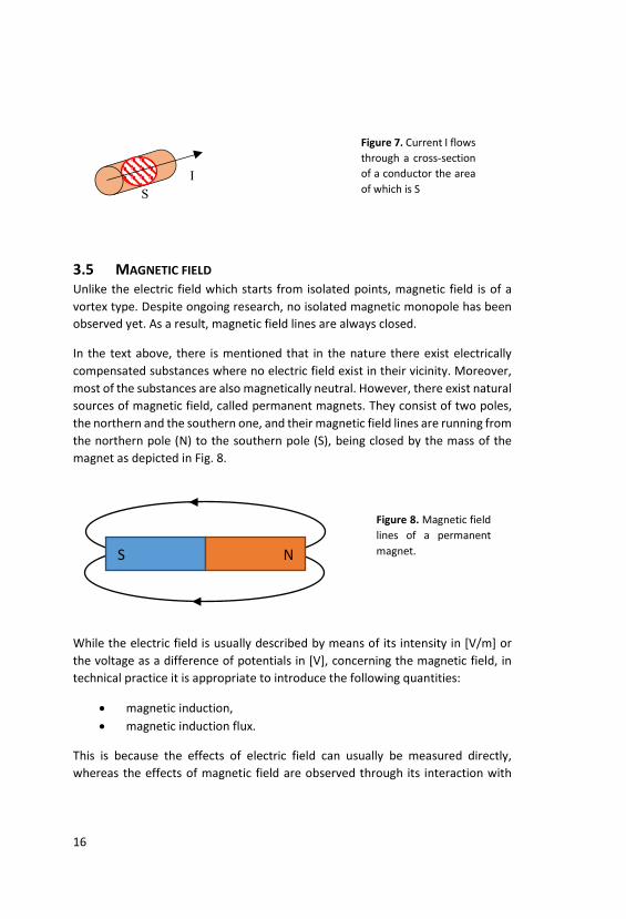
3.4.3 Current density For the purposes of calculations regarding electromagnetic field and many other technical problems, it is a right time to introduce another variable, called current density. It expresses how much of the current flows through the cross sectional area unit of the conductor (see Fig. 7). When the current I flows through a cross-section of a conductor the area of which is S, the current density can be expressed as follows:
𝐽𝐽 =𝐼𝐼𝑆𝑆 [𝐴𝐴 ∙ 𝑚𝑚−2]
(13)
When describing this phenomenon in three-dimensional space, it is useful to consider the current density as a vector 𝐽𝐽. From this point of view, in the conductor there exists a current field 𝐽𝐽. The Ohm’s law (9) can then be expressed in two forms, the integral one (14) and the differential one (15).
𝐼𝐼 =𝑈𝑈𝑅𝑅
[𝐴𝐴] (14)
𝐽𝐽 = 𝛾𝛾𝐸𝐸 [𝐴𝐴 ∙ 𝑚𝑚−2] (15)
Where: I is the current flowing through the conductor in Amperes [A], U is the voltage between the two ends of the conductor in Volts [V], R is the resistance of the conductor in Ohms [Ω], 𝐽𝐽 is the vector of the current field density in Amperes per square meter [𝐴𝐴 ∙ 𝑚𝑚−2], 𝛾𝛾 is the conductivity of the conductor in Siemens per meter [𝑆𝑆 ∙ 𝑚𝑚−1], 𝐸𝐸 is the vector of intensity of electric field in the conductor in Volts per meter [𝑉𝑉 ∙ 𝑚𝑚−1].
16
3.5 MAGNETIC FIELD Unlike the electric field which starts from isolated points, magnetic field is of a vortex type. Despite ongoing research, no isolated magnetic monopole has been observed yet. As a result, magnetic field lines are always closed.
In the text above, there is mentioned that in the nature there exist electrically compensated substances where no electric field exist in their vicinity. Moreover, most of the substances are also magnetically neutral. However, there exist natural sources of magnetic field, called permanent magnets. They consist of two poles, the northern and the southern one, and their magnetic field lines are running from the northern pole (N) to the southern pole (S), being closed by the mass of the magnet as depicted in Fig. 8.
While the electric field is usually described by means of its intensity in [V/m] or the voltage as a difference of potentials in [V], concerning the magnetic field, in technical practice it is appropriate to introduce the following quantities:
• magnetic induction, • magnetic induction flux.
This is because the effects of electric field can usually be measured directly, whereas the effects of magnetic field are observed through its interaction with
S I
S N
Figure 8. Magnetic field lines of a permanent magnet.
Figure 7. Current I flows through a cross-section of a conductor the area of which is S
17
other materials. However, as long as the electric field intensity is expressed in [V/m], the magnetic field intensity can be expressed in [A/m].
The magnetic induction is a vector quantity expressed in Teslas [T]. It describes the effects of the magnetic field on the material through which the magnetic field lines pass:
𝐵𝐵 = 𝜇𝜇0𝜇𝜇𝑟𝑟𝐻𝐻 [T] (16)
Where: µ0 is the permeability of vacuum, 𝜇𝜇0 = 4𝜋𝜋 ∙ 10−7 [𝐻𝐻 ∙ 𝑚𝑚−1], µr is the relative permeability of the material in which the interaction occurs, 𝐻𝐻 is the intensity vector of the magnetic field [A/m].
Because the magnetic field shows the force effects on the moving charged particles, the vector of magnetic induction 𝐵𝐵 is implicitly defined as follows:
𝐹𝐹𝑚𝑚 = 𝑄𝑄𝑣 × 𝐵𝐵 [N] (17)
Where: 𝐹𝐹𝑚𝑚 is the magnetic force acting on a charge Q that moves with the speed 𝑣 in the magnetic field, while the vector of its induction is 𝐵𝐵 . Because the vectors of magnetic induction and particle velocity are multiplied by the vector product, the force 𝐹𝐹𝑚𝑚 is perpendicular to both of the vectors. Therefore it is obvious that the magnetic field can change the trajectory of motion of electrically charged particles, however, it cannot change their speed.
In technical applications, magnetic induction flux is also an important quantity. It indicates how the magnetic induction is projected into the area under magnetic induction lines. Imagine that the magnetic induction B impinges on the surface with area S at α angle (see Fig. 9). The magnetic induction flux, expressed in Webers [Wb] can then be evaluated as follows:
Φ = 𝐵𝐵 ∙ 𝑆𝑆 ∙ sin𝛼𝛼 [Wb] (18)

18
Of course, there are many other quantities, for example magnetic tension or magnetic potential. Introducing them would, however, exceed this brief introduction into electromagnetism.
3.5.1 Magnetic field around conductor Not only are the permanent magnets the sources of the magnetic field. Let us get back to the experiment of Andre Maria Ampére who found out that two conductors flown by the current are attracted or repelled by the force expressed in (12). Later it turned out that the cause of this force is the magnetic field that occurs in the vicinity of the conductor once there is an electric current in it. The magnetic field lines are closed around the conductor as depicted in Fig. 10.
The direction of the magnetic induction lines is determined by the right-hand rule: If the conductor is taken in our right hand in that way the thumb shows the direction of the current (conventional - from positive to negative), the direction of the magnetic flux lines is shown by the rest of the fingers. The level of magnetic induction depends on the current, the distance from the conductor and, finally, on the length of the conductor. Generally, this problem can be solved according to Biot-Savart’s law. For the purposes of our brief description let us only expect that the diameter of the conductor is infinitely small and its length is infinitely great. Then the magnetic induction in the distance a from the conductor will be expressed as follows:
α B
S
Figure 9. Magnetic induction flux
Figure 10. Magnetic induction lines B around the conductor (dotted) which carries electric current I

19
B =𝜇𝜇0𝜇𝜇𝑟𝑟𝐼𝐼2𝜋𝜋𝑔𝑔 [𝑇𝑇] (19)
3.6 QUASI STATIONARY ELECTROMAGNETIC FIELD In the previous chapters the basic phenomena and quantities have been introduced. Except the Faraday’s induction law, all fields were considered as stationary. The intensity of electric field, as well as the magnitude of the magnetic induction or the current passing through a conductor, did not change in time. This was necessary to explain the essence of the above mentioned quantities. However, most effects used in electrical engineering are based on the changes of these quantities in time. Unfortunately, electric and magnetic field can propagate no faster than light. The speed of the light in vacuum is:
c =1
𝜀𝜀0𝜇𝜇0≈ 300,000,000 [𝑚𝑚 ∙ 𝑠𝑠−1] (20)
In natural materials that have some relative permittivity εr and relative permeability µr the propagation velocity will be adequately lower. As a result, when fast changes of electromagnetic fields exist in the circuits, their effects are dependent on time and position, because it takes some time to the stir to spread from the point of origin to the point of observation.
However, the effect of the limited propagation velocity can be neglected if the wavelength of the stir is much longer than the dimensions of the circuit. For example, let us consider power supply network where the frequency of 50 Hz is used. The wavelength of the stir will be:
λ =𝑐𝑐𝑓𝑓 ≈ 6,000 [𝑘𝑘𝑚𝑚] (21)
It is obvious that in a circuit the dimensions of which are in tens of centimetres, the effects of the limited propagation velocity can be neglected. When the circuit operates at the frequency of 50 Hz, all intensity vectors of electric and magnetic fields can be considered the same at every point of the circuit.
The field, the changes of which are slow enough, is called quasi stationary. A typical application of this approach results in the Faraday’s induction law or description of displacement current.
20
3.6.1 Faraday’s law of induction In 1831 Michael Faraday discovered that in a closed electric loop there occurs electric current once there is a magnetic flux variating in time passing through the area of the loop. This effect, called Faraday’s law of induction, has been one of the essential findings at the field of electromagnetism. It is employed in all AC current generators (power plants, car alternators etc.).
The voltage induced in the loop is proportional to the negative change of the magnetic flux passing through its area:
u = −dΦdt [𝑉𝑉]
(22)
The magnetic induction flux is defined by (18), in other words it depends on the area through which the magnetic induction passes, the intensity of the magnetic induction and the angle between the vector of the magnetic intensity and the surface of the area. This allows the construction of rotary AC generators. As the winding of the generator rotates in magnetic field, the angle α permanently changes, which results in sinusoidal voltage occurrence at the output of the generator. On the other hand, this is also a common source of potential problems in terms of electromagnetic compatibility as electronic circuits tend to be driven by voltage induced by magnetic fields that naturally occur when there are AC currents in the circuitry.
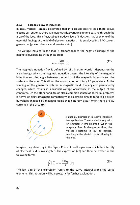
Imagine the yellow ring in the Figure 11 is a closed loop across which the intensity of electrical field is investigated. The expression (22) can then be written in the following form:
E dl = −dΦM
dt [𝑉𝑉] (23)
The left side of the expression refers to the curve integral along the curve elements. This notation will be necessary for further explanation.
A
Φ
Figure 11. Example of Faraday’s induction law application. There is a wire loop with an ammeter A implemented. When the magnetic flux Φ changes in time, the voltage according to (20) is induced, resulting in the electric current flowing in the loop.
21
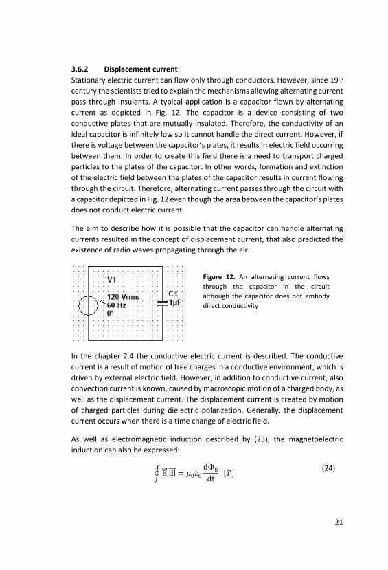
3.6.2 Displacement current Stationary electric current can flow only through conductors. However, since 19th century the scientists tried to explain the mechanisms allowing alternating current pass through insulants. A typical application is a capacitor flown by alternating current as depicted in Fig. 12. The capacitor is a device consisting of two conductive plates that are mutually insulated. Therefore, the conductivity of an ideal capacitor is infinitely low so it cannot handle the direct current. However, if there is voltage between the capacitor’s plates, it results in electric field occurring between them. In order to create this field there is a need to transport charged particles to the plates of the capacitor. In other words, formation and extinction of the electric field between the plates of the capacitor results in current flowing through the circuit. Therefore, alternating current passes through the circuit with a capacitor depicted in Fig. 12 even though the area between the capacitor’s plates does not conduct electric current.
The aim to describe how it is possible that the capacitor can handle alternating currents resulted in the concept of displacement current, that also predicted the existence of radio waves propagating through the air.
In the chapter 2.4 the conductive electric current is described. The conductive current is a result of motion of free charges in a conductive environment, which is driven by external electric field. However, in addition to conductive current, also convection current is known, caused by macroscopic motion of a charged body, as well as the displacement current. The displacement current is created by motion of charged particles during dielectric polarization. Generally, the displacement current occurs when there is a time change of electric field.
As well as electromagnetic induction described by (23), the magnetoelectric induction can also be expressed:
B dl = 𝜇𝜇0𝜀𝜀0dΦE
dt [𝑇𝑇] (24)
Figure 12. An alternating current flows through the capacitor in the circuit although the capacitor does not embody direct conductivity
22
Where ΦE is a flux of electric field through environment. It is equivalent to ΦM and it can be expressed as follows:
ΦM = 𝜀𝜀0𝜀𝜀𝑟𝑟 ∙ 𝑆𝑆 ∙ cos𝛼𝛼 [C] (25)
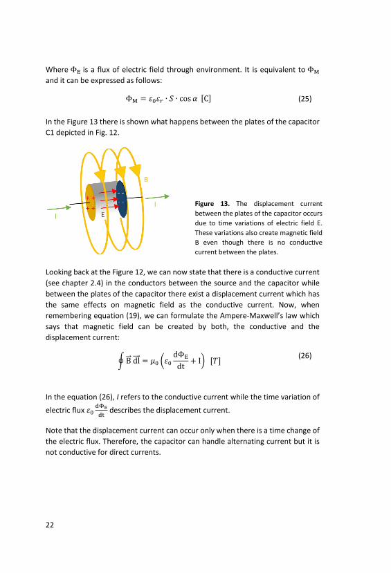
In the Figure 13 there is shown what happens between the plates of the capacitor C1 depicted in Fig. 12.
Looking back at the Figure 12, we can now state that there is a conductive current (see chapter 2.4) in the conductors between the source and the capacitor while between the plates of the capacitor there exist a displacement current which has the same effects on magnetic field as the conductive current. Now, when remembering equation (19), we can formulate the Ampere-Maxwell’s law which says that magnetic field can be created by both, the conductive and the displacement current:
B dl = 𝜇𝜇0 𝜀𝜀0dΦE
dt + I [𝑇𝑇] (26)
In the equation (26), I refers to the conductive current while the time variation of
electric flux 𝜀𝜀0dΦE
dt describes the displacement current.
Note that the displacement current can occur only when there is a time change of the electric flux. Therefore, the capacitor can handle alternating current but it is not conductive for direct currents.
Figure 13. The displacement current between the plates of the capacitor occurs due to time variations of electric field E. These variations also create magnetic field B even though there is no conductive current between the plates.
23
3.7 ELECTROMAGNETIC WAVES The term electromagnetic wave regards to the changes of electric field intensity 𝐸𝐸 and magnetic field induction 𝐵𝐵 in time and space. It is worth mentioning that these two components are mutually dependent, according to the impedance of the environment in which the electromagnetic field propagates. The propagation exists in both, conductive and non-conductive environment, and shows the following features:
• electromagnetic waves can transport energy, • the waves exist only if their source delivers energy, • provided that the environment in which the waves propagate is
homogenous and isotropic, the velocity of propagation is constant.
Generally, the most correct way to describe the propagation of a wave is to use wave equation. It is a second-order hyperbolic partial differential equation which allows to express the actual size and orientation of a vector u in space and time. For the vector u in Euclidean three-dimensional space using the coordinates x, y, z, the following wave equation apply:
𝜕𝜕2𝑢𝑢𝜕𝜕𝑥𝑥2 +
𝜕𝜕2𝑢𝑢𝜕𝜕𝑦𝑦2 +
𝜕𝜕2𝑢𝑢𝜕𝜕𝑧𝑧2 =
1𝑣𝑣2𝜕𝜕2𝑢𝑢𝜕𝜕𝑡𝑡2
(27)
Where v is the propagation velocity and t is time.
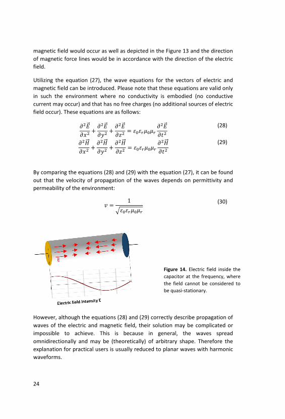
3.7.1 Electromagnetic waves in non-conductive isotropic environment The most striking feature of electromagnetic waves is the fact that they can propagate through non-conductive environment, transporting energy by means of radio waves. In such environment there are no charged particles and therefore no conductivity occurs. Look at the Figure 13. In the chapter 2.6.2 it was stated that there is no conductive current between the plates of the capacitor but the displacement current takes over the transfer of the energy. The magnetic field remains the same around the conductors as well as around the area between the plates of the capacitor, according to the equation (26). Because the plates of the capacitor are close to each other, the electromagnetic field between them can be considered as quasi-stationary. If we increase frequency or push the capacitor’s plates far apart, waves of electric and magnetic field will occur between the plates, because both the electric and the magnetic field cannot propagate faster than the speed of light. The situation for electric field is depicted in the Figure 14. The polarization of the material between the plates of the capacitor is happening at the finite speed which results in a wave propagating through the capacitor. For better clarity there are no magnetic field lines drawn in the picture. In reality, the
24
magnetic field would occur as well as depicted in the Figure 13 and the direction of magnetic force lines would be in accordance with the direction of the electric field.
Utilizing the equation (27), the wave equations for the vectors of electric and magnetic field can be introduced. Please note that these equations are valid only in such the environment where no conductivity is embodied (no conductive current may occur) and that has no free charges (no additional sources of electric field occur). These equations are as follows:
𝜕𝜕2𝐸𝐸𝜕𝜕𝑥𝑥2 +
𝜕𝜕2𝐸𝐸𝜕𝜕𝑦𝑦2 +
𝜕𝜕2𝐸𝐸𝜕𝜕𝑧𝑧2 = 𝜀𝜀0𝜀𝜀𝑟𝑟𝜇𝜇0𝜇𝜇𝑟𝑟
𝜕𝜕2𝐸𝐸𝜕𝜕𝑡𝑡2
(28)
𝜕𝜕2𝐻𝐻𝜕𝜕𝑥𝑥2 +
𝜕𝜕2𝐻𝐻𝜕𝜕𝑦𝑦2 +
𝜕𝜕2𝐻𝐻𝜕𝜕𝑧𝑧2 = 𝜀𝜀0𝜀𝜀𝑟𝑟𝜇𝜇0𝜇𝜇𝑟𝑟
𝜕𝜕2𝐻𝐻𝜕𝜕𝑡𝑡2
(29)
By comparing the equations (28) and (29) with the equation (27), it can be found out that the velocity of propagation of the waves depends on permittivity and permeability of the environment:
𝑣𝑣 =1
𝜀𝜀0𝜀𝜀𝑟𝑟𝜇𝜇0𝜇𝜇𝑟𝑟 (30)
However, although the equations (28) and (29) correctly describe propagation of waves of the electric and magnetic field, their solution may be complicated or impossible to achieve. This is because in general, the waves spread omnidirectionally and may be (theoretically) of arbitrary shape. Therefore the explanation for practical users is usually reduced to planar waves with harmonic waveforms.
Figure 14. Electric field inside the capacitor at the frequency, where the field cannot be considered to be quasi-stationary.
25
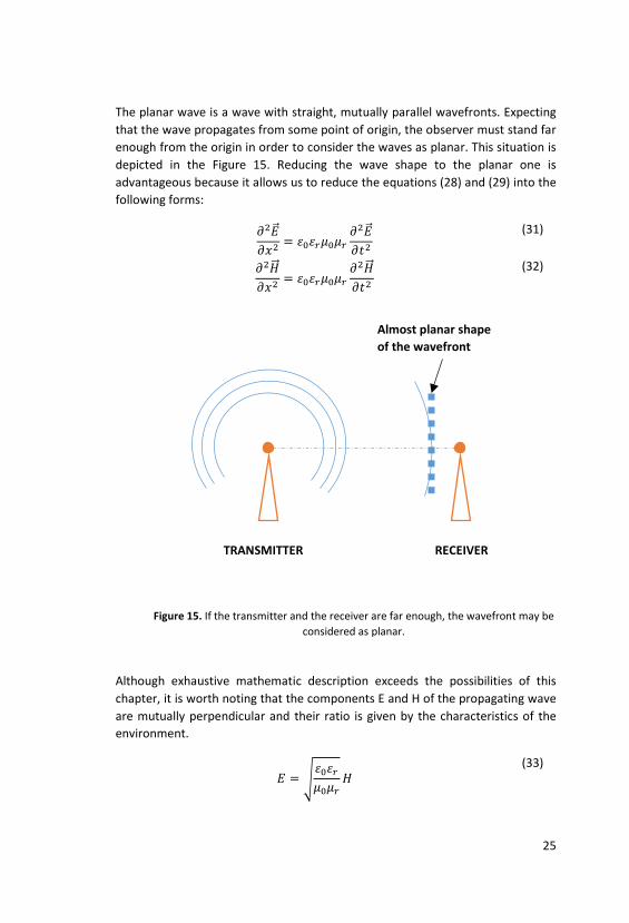
The planar wave is a wave with straight, mutually parallel wavefronts. Expecting that the wave propagates from some point of origin, the observer must stand far enough from the origin in order to consider the waves as planar. This situation is depicted in the Figure 15. Reducing the wave shape to the planar one is advantageous because it allows us to reduce the equations (28) and (29) into the following forms:
𝜕𝜕2𝐸𝐸𝜕𝜕𝑥𝑥2 = 𝜀𝜀0𝜀𝜀𝑟𝑟𝜇𝜇0𝜇𝜇𝑟𝑟
𝜕𝜕2𝐸𝐸𝜕𝜕𝑡𝑡2
(31)
𝜕𝜕2𝐻𝐻𝜕𝜕𝑥𝑥2 = 𝜀𝜀0𝜀𝜀𝑟𝑟𝜇𝜇0𝜇𝜇𝑟𝑟
𝜕𝜕2𝐻𝐻𝜕𝜕𝑡𝑡2
(32)
Although exhaustive mathematic description exceeds the possibilities of this chapter, it is worth noting that the components E and H of the propagating wave are mutually perpendicular and their ratio is given by the characteristics of the environment.
𝐸𝐸 = 𝜀𝜀0𝜀𝜀𝑟𝑟𝜇𝜇0𝜇𝜇𝑟𝑟
𝐻𝐻 (33)
TRANSMITTER RECEIVER
Almost planar shape of the wavefront
Figure 15. If the transmitter and the receiver are far enough, the wavefront may be considered as planar.
26
For vacuum (or the air) the relative permittivity and permeability are equal to 1, resulting in:
𝐸𝐸 = 𝜀𝜀0𝜇𝜇0𝐻𝐻 ⇒ 𝐸𝐸/𝐻𝐻 ≈ 377[Ω]
(34)
From (34) it is obvious that in free air the intensity of electric field is much higher than the intensity of magnetic field, provided the wave is of a planar type. The
ratio 𝜀𝜀0𝜇𝜇0
is usually called “wave impedance of the environment”. Can you see
the equivalence with the Ohm’s law?
Let us make things even simpler and imagine the planar wave is of a sinusoidal shape and propagates along the x-axis. Provided the frequency of the wave is f, the angular frequency of the wave is as follows.
𝜔𝜔 = 2𝜋𝜋𝑓𝑓 (35)
Considering that the components of the electric field are distributed along the axes x, y and z of the Euclidian space, the velocity of propagation is v and the maximum intensities of electric field are Emy for the direction along the y-axis and Emz for the direction along the z-axis. By application of Maxwell’s equations, the components of the electromagnetic field in three-dimensional space can be expressed as follows:
𝐸𝐸𝑥𝑥 = 0 (37)
𝐸𝐸𝑦𝑦 = 𝐸𝐸𝑚𝑚𝑦𝑦 sin 𝜔𝜔𝑡𝑡 − 𝜔𝜔𝑥𝑥𝑣𝑣 (38)
𝐸𝐸𝑧𝑧 = 𝐸𝐸𝑚𝑚𝑧𝑧 sin 𝜔𝜔𝑡𝑡 − 𝜔𝜔𝑥𝑥𝑣𝑣 + 𝜑𝜑 (39)
𝐻𝐻𝑥𝑥 = 0 (40)
𝐻𝐻𝑦𝑦 = −𝜇𝜇0𝜇𝜇𝑟𝑟𝜀𝜀0𝜀𝜀𝑟𝑟
𝐸𝐸𝑚𝑚𝑧𝑧 sin 𝜔𝜔𝑡𝑡 − 𝜔𝜔𝑥𝑥𝑣𝑣 + 𝜑𝜑 (41)

27
𝐻𝐻𝑧𝑧 = 𝜇𝜇0𝜇𝜇𝑟𝑟𝜀𝜀0𝜀𝜀𝑟𝑟
𝐸𝐸𝑚𝑚𝑦𝑦 sin 𝜔𝜔𝑡𝑡 − 𝜔𝜔𝑥𝑥𝑣𝑣 (42)
Where: t is time, x is the actual position at the x-axis in which the wave is observed, ϕ is the phase shift.
The simplest planar wave with harmonic waveform propagating in one direction has one of the components Emy or Emz equal to zero. In this case, the electric component oscillates in one plane while the magnetic component of the field oscillates in second plane. Both planes are mutually perpendicular as well as they are perpendicular to the direction of propagation of the wave. This case is called linearly polarized wave. For the purposes of measurements in the field of electromagnetic compatibility, the linearly polarized waves are essential as they are expected to occur at almost every EMC test. An example of a linearly polarized wave is depicted in Fig. 16.
According to the direction of oscillations of the electrical field, vertical and horizontal polarization is distinguished. Most antennas for electromagnetic compatibility except special military applications are constructed to receive polarized planar waves. If the vector of the electric field 𝐸𝐸 oscillates as depicted in Figure 16, the wave is vertically polarized. If the vector 𝐸𝐸 oscillates according to the z-axis, the wave is horizontally polarized. In most cases, the measurements in EMC laboratories are only done for these two expected polarizations.
When propagating through space, the length of the wave can be simply calculated according to the following equation:
𝜆𝜆 =𝑣𝑣𝑓𝑓 [𝑚𝑚] (43)
where v is the velocity of propagation of the wave and f is its frequency.
Figure 16. Harmonic planar wave propagation in the direction of the x-axis
28
The readers, who are interested in the theory of electromagnetic field may find further information in [5, 8, 9, 10]. Those who do not want to be too familiar with the theory should read the following conclusion at least in order to understand further chapters of this book.
!
1. In nature, materials can be found, in which positively and negatively charged particles can be separated. By this way, an electric charge is obtained. The electric charge is measured in Coulombs [C].
2. Once the electric charge exists, electric field occurs around. Its intensity can be measured in Newtons per Coulomb or Volts per Meter. Electric field can attract or repel other charged particles.
3. The difference of intensity between two different points inside the electric field is called voltage, expressed in Volts [V].
4. The phenomenon where the charged particles pass through the electrical conductor is called an electric current. Its intensity is given by the amount of charge that passes the cross section of the conductor per one second and it is measured in Amperes [A].
5. There is a magnetic field occurrence around the conductor carrying the electrical current. The intensity of the magnetic field is evaluated by its effects on other materials. This effect is called magnetic induction and it is measured in Teslas [T].
6. If the field is stationary (it does not vary in time), its magnetic and electric components may be observed separately as a magnetostatic field and electrostatic field respectively.
7. If the field changes that are slow enough, quasi-stationary concept may be applied. Changes of electric field induce magnetic field and vice versa. The electric and magnetic components of oscillating fields are always closely related.
8. Oscillating electromagnetic field can create displacement current that enables propagation of energy through non-conductive materials.
9. The electromagnetic field can propagate at limited speed. Therefore, the wave nature of the field must be taken in account at high frequencies and/or large distances.
29
4 ELECTROMAGNETIC COMPATIBILITY
In the words “Electromagnetic compatibility”, two meanings are concealed. It is a term describing the ability of electronic devices to operate together with neighbouring devices and at the same time it refers to a scientific discipline that studies all related phenomena. In this discipline, scientific, technical and application knowledge is combined, reaching almost all areas of electrical engineering and electronics: high-current electronics, electricity transferring, radio and telecommunication engineering, information technology, measuring and automation, analogue and digital technology, antenna designs, high-frequency and microwave technology, medical electronics and many other ones. Moreover, significant economical aspect must be taken into account as well.
The first issue of electromagnetic compatibility, the electrostatic discharge (ESD), has been systematically dealt with since the end of 18th century, when several paper mills had faced accidents caused by ignition of the paper dust by spark discharges. Even earlier, the effects on spark discharges on gunpowder have also been known [3].
The history of electromagnetic compatibility as a complex scientific discipline dates back to the 1960s, when it became obvious that increasing number of electronic devices will necessitate introduction of rules introducing requirements on every single electronic device in that way so it would not generate excessive interference and, on the other hand, it would operate correctly even when it is exposed to a certain level of interference. The most critical situation occurred in the field of military technologies as complex and expensive systems were developed and put into operation. Disregard of electromagnetic compatibility issues has led to fatal failures. Let us mention two of them:
• In 1984, the fighterbomber Tornado crashed near Holzkirchen (Germany)after its control systems failed due to intensive radio interferences. InHolzkirchen, there was a powerful transmitter of Radio Free Europe whichattempted to transmit western news over the iron curtain during the coldwar.
• In 1982, during the war on the Falklands, the British cruiser Sheffield wassank after the crew shut down the anti-aircraft system. This happenedbecause the anti-aircraft systems interfered with radio communicationbetween the cruiser and the headquarters. Twenty people lost their lives.
The above mentioned crashes occurred despite the fact that in 1980s the issues on electromagnetic compatibility have been studied for at least twenty years. As
https://doi.org/10.7441/978-80-7454-876-5_2

30
early as in the year 1968, H. M. Schlicke stated: “Any system can be perfectly reliable in itself, however, it become worthless if it is not electromagnetically compatible with other systems and electromagnetic environment (lightning and precipitation static) at the same time. The reliability and the electromagnetic compatibility are the two inseparable requirements on the system that is expected to work safely and reliably at all times and in all circumstances.”
4.1 SUB-DISCIPLINES The scientific discipline of Electromagnetic compatibility can be divided into several sub-disciplines according to phenomena being studied:
1. Electromagnetic compatibility of biological systems 2. Electromagnetic compatibility of technical systems.
While the electromagnetic compatibility of biological systems deals with the influence of electromagnetic field on living organisms, the electromagnetic compatibility of technical systems concerns engineering issues. Although scientists usually find consensus concerning the technical systems, there are many ambiguous issues on the electromagnetic compatibility of biological systems. Despite that the effects of electromagnetic field on the human organism have been observed for a long time, the results of existing biophysical and biophysical research in this area are not unambiguous. The biological effects of the electromagnetic field depend on its nature, the duration of action, and the properties of the organism. Since field receptors (i.e., inputs of the electromagnetic field into the organism) are not known, these effects are only assessed by non-specific reactions of the organism. In most countries, the maximum allowable levels of electromagnetic field that people may be exposed to, are defined by law. Whereas there are no uniform opinions on this issue, these limits may be considerably different across the countries. This gives cause for conspiracy theories. For example, the author of this book has heard a theory that “electrical engineers have conspired and want to reduce birth rates by means of WiFi” and many others. Taking this matter seriously, it can only be said that in the field of compatibility of biological systems a great deal of work is waiting for scientists.
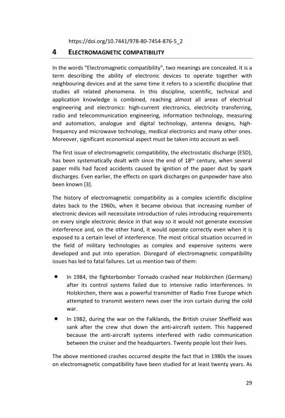
On the other hand, the electromagnetic compatibility of technical systems is much easier to explore, as the characteristics and malfunctions of technical systems are clearly visible and easy to describe. Let us therefore focus only on these issues. Within the technical systems, three essential elements of the issue exist:
• Source of the interference.
31
• Coupling path. • Victim.
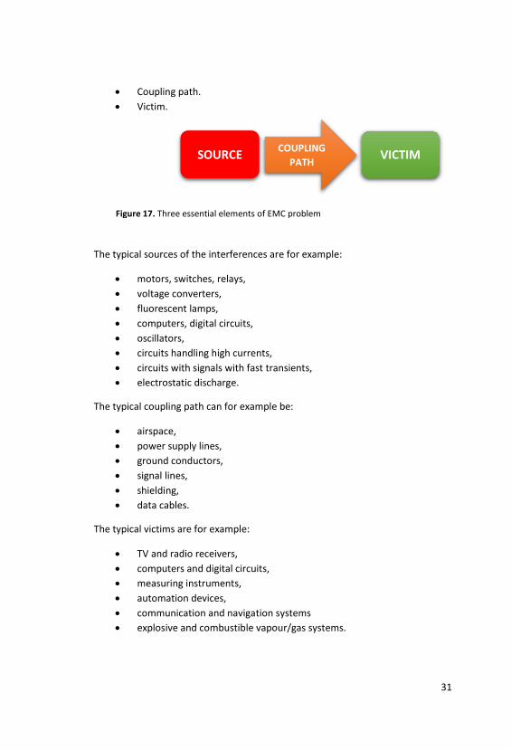
The typical sources of the interferences are for example:
• motors, switches, relays, • voltage converters, • fluorescent lamps, • computers, digital circuits, • oscillators, • circuits handling high currents, • circuits with signals with fast transients, • electrostatic discharge.
The typical coupling path can for example be:
• airspace, • power supply lines, • ground conductors, • signal lines, • shielding, • data cables.
The typical victims are for example:
• TV and radio receivers, • computers and digital circuits, • measuring instruments, • automation devices, • communication and navigation systems • explosive and combustible vapour/gas systems.
SOURCE VICTIM COUPLING PATH
Figure 17. Three essential elements of EMC problem

32
Generally, the electromagnetic compatibility as a discipline is divided into two main blocks:
• electromagnetic interference (EMI), • electromagnetic susceptibility (EMS).
The number of human activities affected by the issues of electromagnetic compatibility is quite large, for example:
• design and construction of electronic devices, • marketing of electronic products, • testing and measurement procedures, • production processes, • communication and information systems, • health protection, • occupational safety, • protection of classified information, • reliability of weapon systems, • security systems, • regulations and legislation.
4.2 ELECTROMAGNETIC INTERFERENCE The electromagnetic interference (EMI) discipline looks at the processes of occurrence and propagation of interferences. Its main responsibility consists in:
• identification of the source of the interference, • measurement of the interferences, • description of the interferences, • identification of all coupling paths, • definition of conditions under which the measurements are processed
in order to ensure their repeatability and informative value.
As mentioned above, the main focus comprises the sources of the interferences and the coupling paths. In other words, the causes of the interferences are addressed. The typical laboratory tests consist of:
• measurement of conducted interferences on power supply lines and data cables,
• measurement of radiated electromagnetic field inside anechoic rooms.
33
4.3 ELECTROMAGNETIC SUSCEPTIBILITY The electromagnetic susceptibility (EMS) discipline studies how the tested device sustains the interferences that intrude from the outside. Since it is unrealistic to assume the environment without any interferences, electronic devices must be constructed in the way so that they sustain a certain levels of interferences. The main responsibility of the EMS discipline therefore consists in:
• classification of interferences that may occur, • definition of requirements on the susceptibility of electronic devices, • definition of certain tests to prove the susceptibility of the devices; these
tests must be exactly defined in order to ensure their repeatability and information value.
It is obvious that the main focus of EMS comprises coupling paths and behaviour of the victim under certain conditions. There are many specific tests for each of the industries. These tests usually have one of the following forms:
• electrostatic discharge, • radiated electromagnetic field in anechoic chamber, • radiated electromagnetic field in transverse electromagnetic cell, • conducted emissions induced to cables, • conducted emissions injected to cables.
For example, the International Electrotechnical Commission (IEC) defines the following tests:
• IEC 61000-4-2: electrostatic discharge immunity test, • IEC 61000-4-3: radiated radio-frequency electromagnetic field immunity
test, • IEC 61000-4-4: electrical fast transient / burst immunity test, • IEC 61000-4-5: surge immunity test, • IEC 61000-4-6: test of immunity to conducted disturbances induced by
radio-frequency fields, • IEC 61000-4-8: power frequency magnetic field immunity test, • IEC 61000-4-9: pulse magnetic field immunity test, • IEC 61000-4-10: damped oscillatory magnetic field immunity test, • IEC 61000-4-11: voltage dips, short interruptions and voltage variations
immunity tests, • IEC 61000-4-12: oscillatory waves immunity test, • IEC 61000-4-13: harmonics and interharmonics including mains
signalling at AC power port, low frequency immunity tests,

34
• IEC 61000-4-14: voltage fluctuation immunity tests, • IEC 61000-4-16: test for immunity to conducted, common mode
disturbances in the frequency range from 0 Hz to 150 kHz, • IEC 61000-4-17: ripple on DC input power port immunity test, • IEC 61000-4-20: emission and immunity testing in transverse
electromagnetic (TEM) waveguides, • IEC 61000-4-21: reverberation chamber test methods, • IEC 61000-4-23: test methods for protective devices for HEMP and other
radiated disturbances, • IEC 61000-4-25: HEMP immunity test methods for equipment and
systems, • IEC 61000-4-27: unbalance immunity test, • IEC 61000-4-28: variation of power frequency, immunity test, • IEC 61000-4-29: voltage dips, short interruptions and voltage variations
on DC input power immunity tests, • IEC 61000-4-34: voltage dips, short interruptions and voltage variations
immunity tests for equipment with input current more than 16 A per phase.
4.4 LIMITS AND FUNCTIONAL CRITERIA There are two basic methods of how to assess whether the device meets the requirements of all relevant standards.
The first method consists in measurement of interference levels comparing them with the prescribed limits. This method is usually best for EMI tests. The level of interferences is usually expressed as maximum intensity of electromagnetic field at a defined distance from the tested device or as maximum voltage measured on device terminals. Because the electric and magnetic field are closely related, in most cases it is sufficient to measure by means of antennas sensitive to electric component of the electromagnetic field as they usually provide stronger voltage at their terminals. However, in several cases where low frequency high currents occur, measurement of magnetic component of the field may also be prescribed by relevant standards.
Since the measured intensities of electric field may vary from 10 µV/m up to 10 V/m, the dynamic range of the test receiver must be reasonably large. This is also the reason why logarithmic units are introduced. Most of the limits are then expressed in dBµV/m in case of electric field and in dBµA/m in case of magnetic field. It is therefore a logarithm of the ratio between the measured voltage (current) at the antenna terminals and the reference level which has been agreed
35
to be as high as 1 µV (1 µA). (At this moment we expect that at the antenna terminals there is the voltage 1 µV when the field intensity is 1 µV/m. In fact, the situation is more complex, involving the quantity called antenna factor. The description is provided in further chapters.) The proper equations are expressed below:
𝐿𝐿𝑣𝑣𝑣𝑣𝑣𝑣𝑣𝑣𝑣𝑣𝑣𝑣𝑣𝑣 = 20 log𝑈𝑈𝑚𝑚𝑣𝑣𝑣𝑣𝑚𝑚𝑚𝑚𝑟𝑟𝑣𝑣𝑚𝑚
1 𝜇𝜇𝑉𝑉 [𝑔𝑔𝐵𝐵] (44)
𝐿𝐿𝑐𝑐𝑚𝑚𝑟𝑟𝑟𝑟𝑣𝑣𝑐𝑐𝑣𝑣 = 20 log𝐼𝐼𝑚𝑚𝑣𝑣𝑣𝑣𝑚𝑚𝑚𝑚𝑟𝑟𝑣𝑣𝑚𝑚
1 𝜇𝜇𝐴𝐴 [𝑔𝑔𝐵𝐵] (45)
When the measurement at the terminals of the device is processed, the levels are also related to the reference values of 1 µV (1 µA). In this case, the correct interpretation of the measured values is determined by the load impedance connected to the terminals. Standardized impedances are used as it will be described in further chapters.
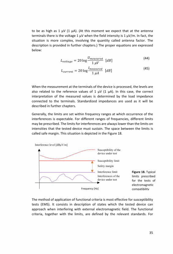
Generally, the limits are set within frequency ranges at which occurrence of the interferences is expectable. For different ranges of frequencies, different limits may be prescribed. The limits for interferences are always lower than the limits on intensities that the tested device must sustain. The space between the limits is called safe margin. This situation is depicted in the Figure 18.
The method of application of functional criteria is most effective for susceptibility tests (EMS). It consists in description of states which the tested device can approach when interfering with external electromagnetic field. The functional criteria, together with the limits, are defined by the relevant standards. For
Frequency [Hz]
Interference level [dBµV/m]
Interference limit
Susceptibility limit
Susceptibility of the device under test
Interferences of the device under test
Safety margin Figure 18. Typical limits prescribed for the tests of electromagnetic compatibility

36
example, the current relevant standard applied in Europe, EN 61000-6-1 ed. 2 defines the following functional criteria:
A degree
The criterion regarding to the A degree is fulfilled if the tested device operates during the test as well as after the test without any malfunctions. Neither a degradation of performance nor functionality loss is allowed, unless an exception is allowed by the manufacturer. It is expected that the device is operated in the manner which it was determined for and all requirements defined in the user’s manual are fulfilled. This is the strictest criterion. The manufacturer may define what changes in operation of the device may occur during the tests, however not affect the functionalities expected from the device by the customer.
B degree
When the tested device is operated according to the user’s manual in the manner which it was determined for, it must work continuously according to its intended purpose during the test. However, certain deterioration of the device’s operation is allowed during the test unless the change of operation state occurs or stored data are lost. The extent of the deterioration of the device’s operation may be defined by the manufacturer. Nevertheless the above mentioned requirements, keeping the operation state and stored data, must always be fulfilled.
C degree
Temporary loss of function during the test is allowed provided that the proper function is restored after the test.
The relevant standards usually define what tests are applicable to which device and what functional criterion must be fulfilled.
4.5 STANDARDS AND LEGISLATION In different countries there are different laws so generalization is not applicable in this chapter. However, in the most of countries the technical standards are not binding unless they are referred to by law. The technical standards are necessary to establish proper communication between engineers and other involved persons and they are used as an invaluable tool helping any technical project to be successful. At the first sight, it is usually not evident how many technical problems are standardized, starting with the dimensions of nuts and bolts, finishing with composition of gasoline.

37
In the field of electromagnetic compatibility, the standardization aims to achieve:
• possibility of comparison of the tested devices, • results that correspond to physical reality, • repeatability of the measurements.
According to the above mentioned, the following issues must be standardized:
• properties of laboratory instrumentation, • measurement procedures, • configuration of the laboratories, • limits and functional criteria.
4.5.1 National and International Standardization bodies Concerning the electromagnetic compatibility, the highest standardization body is the International Electrotechnical Commission (IEC) that has been established in September 1904. This commission is included in the worldwide standardization process that is coordinated by International Organization for Standardization (ISO). Within the International Electrotechnical Commission there exists a specialized radio interference committee the abbreviation of which is CISPR (Comité International Spécial des Perturbations Radioélectriques). This committee issues worldwide valid recommendations that are implemented in national standards afterwards. Within the framework of electromagnetic compatibility issues, the following committees of the above mentioned organizations are the most relevant:
IEC Technical Committees:
• TC 77 Electromagnetic compatibility o SC 77A: Low frequency phenomena, o SC 77B: High frequency phenomena, o SC 77C: High power transient phenomena.
CISPR:
• CIS/A: radio-interference measurements and statistical methods, • CIS/B: interference relating to industrial, scientific and medical RF
apparatus, • CIS/D: EM disturbances related to electric and electronic equipment on
vehicles and devices powered by internal-combustion engines, • CIS/F: interference relating to household appliances, tools, lighting and
similar equipment,
38
• CIS/H: limits for the protection of radio services, • CIS/I: EMC of information technology equipment (ITE), multimedia
equipment and receivers.
The coordination between the IEC and CISPR is supervised by Advisory Committee on Electromagnetic Compatibility (ACEC).
Most of the national and international standards concerning the electromagnetic compatibility are based on the outputs of the above mentioned organizations. However, the processes of standardization on national levels vary depending on the country where they are being used.
For example, in the European Union there exists a special Committee CENELEC (Comitté Européen de Normalisation en Electrotechnique) that generates European Standards. Their numbering begins with the abbreviation EN. These standards are implemented using national standards of member countries according to regulations valid in the European Union. As an example of this process, let us trace the standard ČSN EN 55016 used in the Czech Republic, issued in the Czech language. This standard relates to measuring devices, laboratory equipment, methods in EMC measurements etc.:
1. The CISPR Committee issues a recommendation CISPR 16. 2. The CENELEC Committee checks its applicability in the countries of the
European Union and issues the European Standard EN 55016. 3. The responsible authorities in the Czech Republic must implement this
standard in the Czech standardization system. Currently, it is implemented under the number ČSN EN 55016.
In the field of telecommunications, also the International Telecommunications Union (ITU) is active, involving the following sectors:
• ITU-R (Radiocommunication), • ITU-D (Telecommunication Development) and • ITU-T (Telecommunication Standardization).
Within the European Union, the ITU recommendations are recognized and validated by European Telecommunications Standards Institute (ETSI) that creates European standards for telecommunications and radiocommunications.
As mentioned above, the current standardization system is coordinated by several international organizations. However, the national authorities, called National Standards Bodies (NSB), are active in individual countries. Below there is an

39
example of these institutions, all members of ISO that may be frequently met by the reader:
• AENOR: Spain • AFNOR: France • DIN: Germany • ÚNMZ: Czech Republic • ANSI: USA • SAC: China • GOST R: Russian Federation • SNV: Switzerland • BSI: United Kingdom of Great Britain and Northern Ireland • JISC: Japan • SCC: Canada • SA: Australia
4.5.2 Legally defined requirements As stated in the previous chapters, the standards themselves are usually (depending on country’s legislation) not mandatory, unless they become a part of the contract or are referenced by law. In most countries, there are laws referring to relevant standards, ensuring that a device that is being placed on the market fulfils the relevant requirements concerning the EMC issues. Usually, this is the responsibility of the vendor.
For example, the products placed on the market in European Economic Area must be affixed with CE marking, which is a sign of conformity (Conformité Européenne) with the requirements defined by relevant laws. This mark indicates the conformity with health, safety and environmental protection standard, including the electromagnetic compatibility issues. By affixing the CE marking on a product, a manufacturer effectively declares, at its sole responsibility, conformity with all of the legal requirements to achieve CE marking. This allows free movement and sale of the product throughout the European Economic Area. The manufacturer must carry out a conformity assessment, set up a technical file and sign a Declaration stipulated by the leading legislation for the product. The documentation has to be made available to authorities on request. By marketing the products under their own name, the importers or distributors take over the manufacturer's responsibilities. In this case they must have sufficient information on the design and production of the product, as they will be assuming the legal responsibility when they affix the CE marking.

40
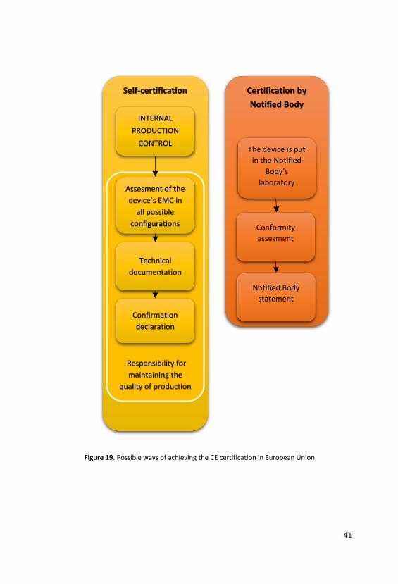
There are two ways of how to reach the certification in the field of EMC:
• Certification issued by notified body, • Self-certification.
The self-certification means that the manufacturer or the vendor of the products declares conformity with all the relevant standards by itself and assumes full responsibility for doing so. This approach is, however, not applicable for all products on the market. If the operation of the products may be critical for safety, for example radio and/or telecommunication devices, products of aviation engineering etc., they must always be certified by notified body of the relevant country.
A notified body, in the European Union, is an entity that has been accredited by a Member State to assess whether a product to be placed on the market meets certain preordained standards. Conformity assessment can include inspection and examination of a product, its design, and the manufacturing environment and processes associated with it. In the USA, the compliance with relevant EMC standards is declared by Federal Communications Commission Declaration of Conformity (FCC). The FCC label or the FCC mark is a certification mark employed on electronic products manufactured or sold in the United States which certifies that the electromagnetic interference from the device is under limits approved by the Federal Communications Commission. By law, the certification must be performed for devices as follows: IT equipment, switched-mode power supplies, monitors, TV receivers, cable system devices, low-power transmitters, unlicensed personal communication devices and industrial, scientific and medical devices that emit radio frequency radiation.
Similarly, the declaration of conformity with the required regulations is expressed in other countries of the world:
• CCC certification mark for China, • VCCI certification mark for Japan, • KC mark for South Korea, • ANATEL mark for Brazil, • BSMI mark for Taiwan.
41
Self-certification Certification by Notified Body
INTERNAL PRODUCTION
CONTROL
Responsibility for maintaining the
quality of production
Assesment of the device’s EMC in
all possible configurations
Technical documentation
Confirmation declaration
Conformity assesment
Notified Body statement
The device is put in the Notified
Body’s laboratory
Figure 19. Possible ways of achieving the CE certification in European Union

42
4.5.3 Hierarchy of standards The currently used sets of standards are hierarchical, so there are standards that are subordinate to or superseded by other standards. There are three levels of hierarchy, concerning the EMC issues:
• Basic standards, • Generic standards, • Product standards.
The basic standards define the issues falling within the area of electromagnetic compatibility, conditions necessary to achieve the compatibility, test and measurement methods, requirements on testing and measurement instruments, nomenclature etc. The basic standards are valid for all products on the market, however they do not define any criterions or limits.
Figure 20. CE mark with proper dimensions. Some attempts to confuse this mark with the „China Export“ mark, having different proportions, have been indicated.
Figure 21. FCC mark

43
The generic standards define requirements and test methods for all technical appliances that are operated in certain environments. Usually, these are distinguished as follows:
• residential environment, • office environment, • light industry, • industrial environment.
The product standards define requirements and test methods for a particular product or product group. These standards are always compliant with the generic standards. They may, however, define more accurate or specific requirements if needed in case of a particular product. The example of product groups is as follows:
• computers and multimedia, • lights, • household appliances, • medical instruments.
A certain hierarchy can also be traced in the harmonization of standards across relevant institutions. For example, in terms of EMC in the European Union, the CENELEC-origin standards begin with the number EN 50000, while CISPR standards begin with EN 55000. In Europe, the IEC standards begin with EN 60000 and the relevant number of the original IEC standard is added. As an example, the IEC 1000 basic standard, defining the basic EMC nomenclature, is in the European Union implemented as EN 61000.
BASIC STANDARDS
GENERIC STANDARDS
PRODUCT STANDARDS
Figure 22. Standards‘ hierarchy

44
In the USA, the most common standard regulating unlicensed radio-frequency transmissions, both intentional and unintentional, is FCC 15.
4.5.4 Military and other special standards Many world’s armies apply so called military standards that are usually rather different from the civil standards discussed above. The military standards can be considered to be the forerunner of all standards on electromagnetic compatibility, since in military applications the need for normalization has appeared first. Within the North Atlantic Alliance armies, the EMC standard MIL-STD 461 as amended is widely applied. These standards are translated into national languages of the member states.
The military standards usually differ from the civil ones in the following attributes:
• peak detectors are used to measure the interference levels, • the limits are more strict, • the frequency ranges are wider, • the test procedures are different, • for measurements of the interferences, there are exact dimensions and
antenna design set. This is because the measurement is performed from the distance of 1 m and the close-field effects occur.
The other area using specific standards is automotive industry. Usually two kinds of testing are applied there. The separated devices, as control units, lamps, etc. are usually tested on their own, as they are usually produced by subcontractors who are responsible for maintaining the required parameters. In this way, the car manufacturers may set their own internal standards that may be (and usually are) more strict than the standards required by law. These standards are then applied to subcontractor products, allowing the manufacturer to gain some “safety” margin. Once the car is completed, it is tested as a whole according to relevant standards again. At present, this is rather a fun procedure, as the number of electronic components implemented in the cars is rather large, they interact each to other and the metal body often changes the nature of the emitted emissions quite unpredictably.
Except for standards for individual components for automotive industry there also exist standards for the whole vehicles. In 1958, an agreement called Agreement Concerning the Adoption of Uniform Conditions of Approval and Reciprocal Recognition of Approval for Motor Vehicle Equipment and Parts was put into effect. As an evolution of this agreement, there exists Regulation 10 by The United Nations Economic Commission for Europe (UNECE). This regulation is called
45
„Uniform provisions concerning the approval of vehicles with regard to electromagnetic compatibility“. It is available online.
Special care must also be taken in case of telecommunication and radiocommunication devices as there exists a large group of standards defined by International Telecommunications Union and moreover, if the radiated emissions are intentional, i.e. the device products radio frequencies to establish the communication, further standards are usually applied.
46
5 CONDITIONS IN EMC LABS
Special laboratory equipment is needed for most of the measurements concerning EMC. The requirements on this equipment are usually defined in the relevant standards. For example, the civil laboratories are usually compliant with the standard CISPR 16 (EN 55016 within the European Union). In this chapter the most common configurations to be met are described.
Since the first measurement was carried out in the open air, the Open Area Test Site (OATS) achieving relevant and repeatable results has been developed as a standard for EMC measurements. The measurement at this site is performed in the open air, assuming the waves are emitted from the tested device, pass around the measurement antenna and continue to infinity, not being reflected. However, there are certain problems that are difficult to solve in this area. The most stressing problem is the intensity of the surrounding electromagnetic field caused by extraneous sources. Therefore, in the course of time, anechoic and semi-anechoic rooms have been developed for the purposes of measurement of the radio frequency fields. These rooms eliminate the most troublesome problems of the open area test sites, but they also suffer from standing waves occurrence, as the damping of the reflections cannot achieve endless value due to physical principles. Both, the open area test site and the semi-anechoic and anechoic rooms, are introduced below.
5.1 OPEN AREA TEST SITE Such a test site is described by CISPR 16 as follows. The ground of the site is ellipse-shaped. The main length of the ellipse is equal to twice the distance between the tested device and the receiving antenna. The distance between the antenna and the device is called the measuring distance D. Only one of these distances may be applied: 100, 30, 10 or 3 m. A usual rule is that the higher is the measurement distance, the better results (see chapter 2.7.1, Fig. 15). On the other hand, large distances as 100 m are quite impractical for some measurements, so the distance 30 or 10 m is widely preferred. The distance of 3 meters is also allowed, but not recommended for measurements at low frequencies as the measurement may be affected by close-field effects (for example, at the frequency of 30 MHz the length of the wave is approximately 10 m). Such a test site must be positioned at a flat and straight terrain where no buildings, power lines, trees or any other electromagnetically reflexive elements are present. Another condition that is currently difficult to fulfil is that the surrounding electromagnetic field (TV, radio, GSM,…) must be small enough not to distort the measured results. It is required that the electromagnetic field not generated by the tested device is at least 20 dB
https://doi.org/10.7441/978-80-7454-876-5_3

47
lower than the measured field. However, this requirement is usually not possible to fulfil. The solution consists in measurement of the extraneous field and excluding of certain frequencies from the test protocol. These problems usually occur with large objects to be measured, for example rail vehicles that usually cannot be taken into anechoic room.
The ground of the open area test site generally acts as a reflector. Consequently, the receiving antenna captures two of the waves: one running directly from the tested device to the antenna, the second one reflected from the ground. As these waves may meet with any mutual phase, the field at the point of antenna may
DuT
2D
h DuT
D
Receiving antenna Device under Test
D/2 √3 D
Wooden table
Direct wave
Reflected wave
Figure 23. Open area test site configuration and dimensions; the dimension D is the measurement distance, values of 3, 10, 30 and 100 m are allowed. The height of the antenna h varies from 1 to 4 meters when D = 3 or D = 10 m and from 2 to 6 meters when D > 10 m.
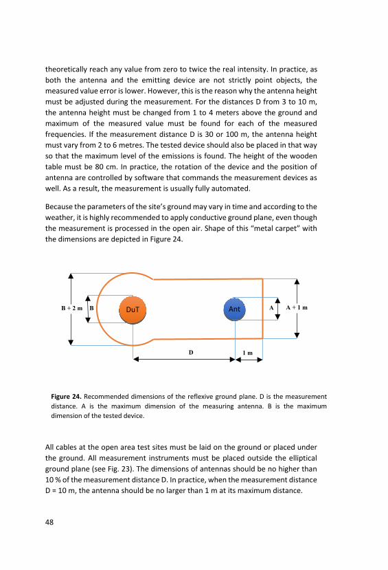
48
theoretically reach any value from zero to twice the real intensity. In practice, as both the antenna and the emitting device are not strictly point objects, the measured value error is lower. However, this is the reason why the antenna height must be adjusted during the measurement. For the distances D from 3 to 10 m, the antenna height must be changed from 1 to 4 meters above the ground and maximum of the measured value must be found for each of the measured frequencies. If the measurement distance D is 30 or 100 m, the antenna height must vary from 2 to 6 metres. The tested device should also be placed in that way so that the maximum level of the emissions is found. The height of the wooden table must be 80 cm. In practice, the rotation of the device and the position of antenna are controlled by software that commands the measurement devices as well. As a result, the measurement is usually fully automated.
Because the parameters of the site’s ground may vary in time and according to the weather, it is highly recommended to apply conductive ground plane, even though the measurement is processed in the open air. Shape of this “metal carpet” with the dimensions are depicted in Figure 24.
All cables at the open area test sites must be laid on the ground or placed under the ground. All measurement instruments must be placed outside the elliptical ground plane (see Fig. 23). The dimensions of antennas should be no higher than 10 % of the measurement distance D. In practice, when the measurement distance D = 10 m, the antenna should be no larger than 1 m at its maximum distance.
DuT Ant
D
A A + 1 m B B + 2 m
1 m
Figure 24. Recommended dimensions of the reflexive ground plane. D is the measurement distance. A is the maximum dimension of the measuring antenna. B is the maximum dimension of the tested device.
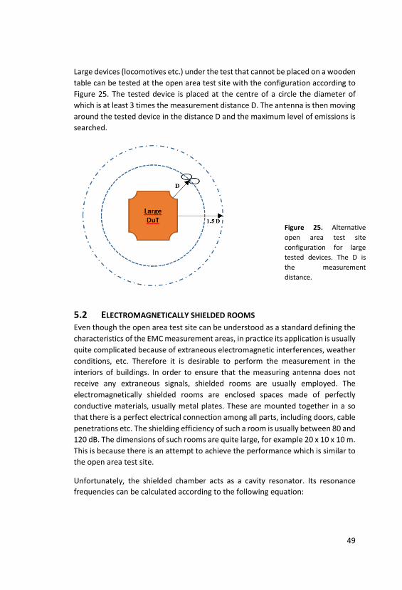
49
Large devices (locomotives etc.) under the test that cannot be placed on a wooden table can be tested at the open area test site with the configuration according to Figure 25. The tested device is placed at the centre of a circle the diameter of which is at least 3 times the measurement distance D. The antenna is then moving around the tested device in the distance D and the maximum level of emissions is searched.
5.2 ELECTROMAGNETICALLY SHIELDED ROOMS Even though the open area test site can be understood as a standard defining the characteristics of the EMC measurement areas, in practice its application is usually quite complicated because of extraneous electromagnetic interferences, weather conditions, etc. Therefore it is desirable to perform the measurement in the interiors of buildings. In order to ensure that the measuring antenna does not receive any extraneous signals, shielded rooms are usually employed. The electromagnetically shielded rooms are enclosed spaces made of perfectly conductive materials, usually metal plates. These are mounted together in a so that there is a perfect electrical connection among all parts, including doors, cable penetrations etc. The shielding efficiency of such a room is usually between 80 and 120 dB. The dimensions of such rooms are quite large, for example 20 x 10 x 10 m. This is because there is an attempt to achieve the performance which is similar to the open area test site.
Unfortunately, the shielded chamber acts as a cavity resonator. Its resonance frequencies can be calculated according to the following equation:
Figure 25. Alternative open area test site configuration for large tested devices. The D is the measurement distance.

50
𝑓𝑓𝑖𝑖𝑖𝑖𝑖𝑖 =𝑐𝑐
2𝜋𝜋√𝜇𝜇𝑟𝑟𝜀𝜀𝑟𝑟
𝑖𝑖𝜋𝜋𝐿𝐿2
+ 𝑗𝑗𝜋𝜋𝐻𝐻
2+
𝑘𝑘𝜋𝜋𝑊𝑊
2
[𝐻𝐻𝑧𝑧] (46)
where:
c is the propagation velocity of the wave in vacuum[𝑚𝑚 ∙ 𝑠𝑠−1], i, j, k are wave indexes specifying how many times the wave fits between the resonator boundaries (case i = 0, j = 0 and k = 0 is forbidden), L is the length of the resonator [m], H is the height of the resonator [m], W is the width of the resonator [m], ε0 is permittivity of vacuum, 𝜀𝜀0 = 8.854 [𝐹𝐹 ∙ 𝑚𝑚−1] , εr is relative permittivity of the material inside the resonator.
The number of resonance frequencies inside the shielded room is quite great. The lowest resonance frequency that may occur in the room (there is one half of the wave between the most distant borders of the resonator) is called dominant mode. For example, at the Tomas Bata University in Zlin there is a shielded room Frankonia SAC 3+ the internal dimensions of which are approximately 10 x 6.5 x 9.5 m (length x width x height). As a result, the dominant mode of the room is approximately f101 = 27.7 MHz, which was also confirmed by sets of measurements. The Figure 26 shows what is wrong when reflections inside the shielded room occur. The shielded room does not only let the electromagnetic waves from the outside get inside, but it also reflects the inner wave propagating out of the source back to the space of the room, not allowing it to continue to infinity (as in the case of the open area test site). As a result, multiple reflections occur inside the room. Moreover, when the room is in resonance at any of the frequencies described by the equation (46), standing waves occur inside, resulting in multiplicative effect of the field intensity. A simulation of electric field for frequencies f101 and f013 is provided in the Figure 27.
In practice, the multiple reflections and standing wave effects lead to the measurement inaccuracy as high as ± 20 dB. This is a considerably large number, indicating that it is not sufficient to use the electromagnetically shielded room without further adjustments.
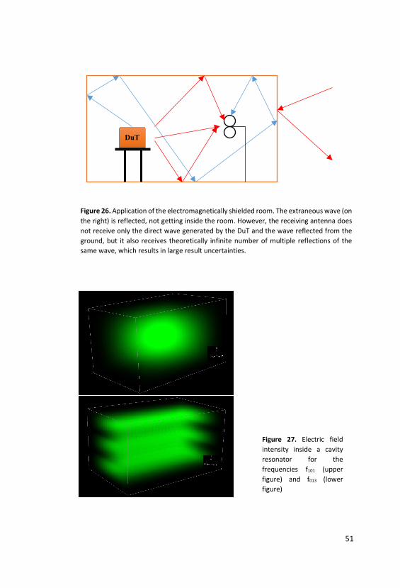
51
DuT
Figure 26. Application of the electromagnetically shielded room. The extraneous wave (on the right) is reflected, not getting inside the room. However, the receiving antenna does not receive only the direct wave generated by the DuT and the wave reflected from the ground, but it also receives theoretically infinite number of multiple reflections of the same wave, which results in large result uncertainties.
Figure 27. Electric field intensity inside a cavity resonator for the frequencies f101 (upper figure) and f013 (lower figure)
52
5.3 ANECHOIC AND SEMI ANECHOIC ROOMS The problems with resonances and reflections that arise from the construction of electromagnetically shielded rooms are sufficiently eliminated by constructions known as anechoic and semianechoic rooms. The outer construction of the anechoic and semianechoic rooms is the same as in the case of electromagnetically shielded rooms. However, the inner surfaces of these rooms are covered with absorbers that consume most of energy of the electromagnetic waves, resulting in considerable limitation of reflections inside the room.
The design of the absorbers is based on the fact that the wave impedance of the air is approximately Z0 = 377 Ω (see (34) in the chapter 2.7.1). If an electromagnetic wave propagates through an environment and meets the interface with different impedance, only part of its energy passes through while the second part is reflected back. The ratio between the permeating and the reflected wave is described by reflection factor ρ:
𝜌𝜌 =𝑍𝑍𝐿𝐿 − 𝑍𝑍𝑚𝑚𝑍𝑍𝐿𝐿 + 𝑍𝑍𝑚𝑚
(47)
Where: ZL is the impedance of the load (material of the room’s wall) in Ohms [Ω], ZS is the impedance of the source (free air inside the room) in Ohms [Ω].
It is obvious that if the walls of the room are conductive very well (their impedance ZL → 0), the refection factor ρ → -1, which is in compliance with what is written above, i.e. there occurs multiple reflections inside the shielded room. The goal is to find such impedance ZL that allows to achieve ρ → 0. This is not achievable directly as there are no materials showing ZL → 0. Fortunately, alternative solutions exist, based on a gradual transformation of impedance.
One of the solutions consists in application of pyramidal absorbers (Fig. 28 and 29) that are mounted on the walls of the room, creating a lossy wave guide. This wave guide is short-circuited at its end by the metal wall of the room. However, the wave must past through its mass there and back, which results in considerable energy losses. In other words, the energy of the electromagnetic wave is wasted in the form of heat. The length of the lossy wave guide must be sufficient in order to achieve satisfactory attenuation. Generally, at least ¼ of the greatest wavelength is usually required.

53
Another solution consists of tiles made of materials with different electrical properties that are glued together. An example of such a tile is depicted in the Figure 30. It consists of 3 different materials with relative permittivities εr1, εr2 and εr3 and dissipation factors tg δ1, tg δ2 and tg δ3. Because the relative permittivity of the air is εr ≈ 1, the relative permittivity of the first material should be low in order to achieve the impedance matching between the free air and the material.
Metal wall
Z → 0
Free space Z → 377 Ω
L
Lossy wave guide
Propagating wave
Reflected wave
Figure 28. Principle of pyramidal absorbers
Figure 29. Set of pyramidal absorbers

54
For the electric parameters of the materials the following should apply: εr1 < εr2 < εr3 and tg δ1 < tg δ2 < tg δ3.
Inside the anechoic and semianechoic rooms, also ferrite absorbers (Fig. 31) can be found. When not magnetized, ferrites cause high losses materials for magnetic fields. Due to their permittivity and permeability ratio, the characteristic impedance may lie close to the impedance of free air space (377 Ω). However, the price of ferrite cladding is considerably high. Therefore the ferrites are used in combination with other types of absorbers, mainly the pyramidal ones.
Currently, the most widespread absorbers are the pyramidal ones, based on foam or polystyrene. They are considerably cheap and have advantageous values of the relative permittivity εr.
Metal wall Z → 0
Free space Z → 377 Ω
εr1
tg δ1 εr2
tg δ2 εr3
tg δ3 Propagating wave
Reflected wave
Figure 30. Multi-material lossy tiles

55
The amount of absorbers implemented inside the room depends on the room’s usage. Usually, the rooms are basically constructed as semi anechoic. While their walls and their ceilings are covered by the absorbers, there is a conductive metal ground plane on the floor. This configuration makes it possible to achieve conditions similar to the open area test site (see chapter 4.1). According to most standards, this configuration is mandatory for measurements of radiated emissions in the range from 30 MHz up to 1 GHz.
Other measurements are performed in fully anechoic rooms where the conductive ground plane is covered by the absorbers as well. This configuration is mainly suitable for antenna measurements and performing of susceptibility tests, because the reflections inside the room may affect the antenna’s performance.
In the Figure 32 there is an example of interior of a semi-anechoic room that may be converted to fully anechoic one by placing additional absorbers on the floor.
Figure 31. Ferrite absorbers
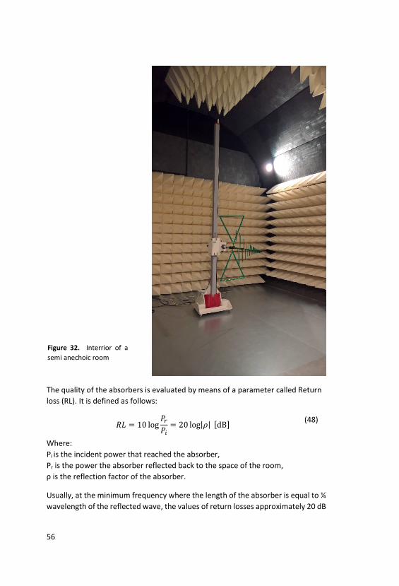
56
The quality of the absorbers is evaluated by means of a parameter called Return loss (RL). It is defined as follows:
𝑅𝑅𝐿𝐿 = 10 log𝑃𝑃𝑟𝑟𝑃𝑃𝑖𝑖
= 20 log|𝜌𝜌| [dB] (48)
Where: Pi is the incident power that reached the absorber, Pr is the power the absorber reflected back to the space of the room, ρ is the reflection factor of the absorber.
Usually, at the minimum frequency where the length of the absorber is equal to ¼ wavelength of the reflected wave, the values of return losses approximately 20 dB
Figure 32. Interrior of a semi anechoic room

57
are achieved. With increasing frequency the return losses also increase. As a result, most problems with reflections inside anechoic rooms occur close to their lowest operating frequency.
There was an experiment held at the Tomas Bata University in Zlin inside the room depicted in the Figure 32. It consisted in measurement of the frequency response of the room at different parts of the room. Inside the room, electromagnetic field was driven by antenna placed at one unchangeable point while the intensities of the field were measured by means of anisotropic probe placed subsequently at 15 different points in the room, always in the same height. The results are depicted in the Figure 33. The location of each graph corresponds to the position of the probe relative to the ground plan of the room. It is worth noting that the room was in semi anechoic configuration (no absorbers on the floor) and the measurement was run within the frequency range from 10 MHz up to 80 MHz, although the lowest applicable frequency of the room is 30 MHz. The frequency range was deliberately chosen between these limits because there was an attempt to map the room’s behaviour in neighbourhood of its dominant resonance frequency, which is approximately 27.7 MHz. The results of the measurement show that effects of reflections decrease with increasing frequency.
Although the performance of the absorbers at low frequencies is not perfect, it is still satisfactory for EMC measurements. Because the configuration during EMC tests is strictly given, the positions of the antenna and the device under test is the same as in case of open area test site (Fig. 23) and the response of the room may partially be eliminated by calibration of the measurement site (see chapter 4.5).

58
Figure 33. Various frequency responses measured at different positions inside the same semi-anechoic room.

59
5.4 ELECTROMAGNETIC REVERBERATION ROOMS Unlike the anechoic rooms, the reverberation rooms are constructed specifically so that the reflections inside are as large as possible. Employing standing waves, they enable to reach very high electromagnetic field intensities. This is useful for some susceptibility tests. The shape of the reflective walls is designed in a way so that as much resonant frequencies were achieved as possible (remember equation (46)).
Because the high quality cavity resonator still resonates at single frequencies (given by the dimensions), one or more tuning elements are usually implemented inside the room. They are called stirrers. They are operated by step motors, enabling to modify geometry the reflections depend on.
A schematic diagram of the electromagnetic reverberation room is shown in the Figure 34.
5.5 ATTENUATION OF THE MEASUREMENT SITE There are standardized rules applied for all kinds of measurement sites. The standard for these is CISPR 16-1. The frequency dependent attenuation of the site must be checked and compared with the theoretically obtained values at each of the measurement sites. This is a condition necessary to ensure that the measured values are really indicative.
The theoretical site attenuation can be calculated on the basis of the following equation:
Figure 34. Schematic diagram of an electromagnetic reverberation chamber

60
𝑃𝑃𝑟𝑟 = 𝑃𝑃𝑣𝑣𝐺𝐺TA𝐺𝐺RA 𝜆𝜆
4𝜋𝜋𝜋𝜋2
[𝑊𝑊] (49)
Where: Pr is the power received by the receiving antenna RA, Pt is the radiated power, GTA is the gain of the transmitting antenna TA, GRA is the gain of the receiving antenna RA, λ is the length of the wave (see (43)), D is the distance between the transmitting antenna TA and receiving antenna RA.
It is worth noting that the antennas TA and RA have no gain in terms of amplification of the signal. However, their spatial radiation patterns may be formed in a way that they are more sensitive in one direction. Since the energy is not spread equally around the antenna, in one of the directions it seems that the antenna shows certain gain. In this case, the gain is the ratio between the energy emitted by directional antenna in the direction of its main lobe and the energy that would be radiated in the same direction by the antenna that is perfectly isotropic.
Based on (49), the theoretical site attenuation SAt can be expressed as follows:
𝑆𝑆𝐴𝐴𝑣𝑣 = 10 log𝑃𝑃𝑣𝑣𝑃𝑃𝑟𝑟
= 10 log 4𝜋𝜋𝑟𝑟𝜆𝜆
2− 10log(𝐺𝐺TA𝐺𝐺RA) [𝑔𝑔𝐵𝐵]
(50)
The expression (50) can be furthermore expressed in the following way, using mathematical treatment and allowing simple values inserting:
𝑆𝑆𝐴𝐴𝑣𝑣[𝑔𝑔𝐵𝐵] = 20 log𝜋𝜋 [𝑚𝑚] + 20 log 𝑓𝑓 [𝑀𝑀𝐻𝐻𝑧𝑧] − 𝐺𝐺𝑇𝑇𝑇𝑇 [𝑔𝑔𝐵𝐵] − 𝐺𝐺𝑅𝑅𝑇𝑇 [𝑔𝑔𝐵𝐵]
− 27.6 − 10 log 1 −𝜋𝜋𝜋𝜋𝑟𝑟 [𝑔𝑔𝐵𝐵]
(51)
Where D is the distance between the transmitting and receiving antenna where the direct wave runs through, while Dr is the direction in which the wave reflected from the ground (see Fig. 23) must run through. In other words, the last logarithm takes into account the influence of the reflective ground floor in semianechoic rooms and at open area test sites.
In the second step, the real attenuation of any measurement site SAr needs to be measured and compared to the theoretical values obtained by (51). The measurement is done in the following way: instead of the tested device (DuT), the transmitting antenna with the known antenna factor GTA is placed and the

61
transmitted signal is received by receiving antenna with the known antenna factor GRA. According to the standard CISPR 16-1, the site may be used for EMC measurements only when the following requirement is fulfilled:
|𝑆𝑆𝐴𝐴𝑣𝑣 − 𝑆𝑆𝐴𝐴𝑟𝑟| ≤ 4 [𝑔𝑔𝐵𝐵] (52)
This is quite a strict requirement: the measurement site must not differ more than by ± 4 dB from the theoretically ideal measurement site. In other words, the measurement uncertainty caused by behaviour of the measurement site cannot be larger than ± 4 dB. Only the actual attenuation of the site is taken into account as it is expected that corrections on antennas sensitivity (antenna factors) GTA, GRA are properly made by inserting the proper values into (51). Because this concept does not depend on antenna properties, it is called normalized site attenuation.
5.6 EMC LABS INSTRUMENTATION A vast number of different instruments are needed to cover the requirements of all conceivable standards. The most used instruments can be divided into the following groups:
• interference meters, • interference generators, • antennas, • near-field probes, • tools for measurement of conducted interferences, • other.
In the following subchapters, a brief description of the most important instruments is provided.
5.6.1 Interference meters The interferences may be observed in both the time and the frequency domains. While oscilloscopes are needed to show the waveform of the interfering signal in the time domain, spectrum analysers and EMI receivers are needed for observation of the signal in frequency domain. In terms of the EMC standards, the frequency domain is the most important and for most of the measurements, EMI receivers are necessary. However, for indicative measurement, for example during research and development, ordinary spectrum analyser may also be a sufficient tool.
In terms of certification, EMI receivers are absolutely necessary and no EMC laboratory can do without them. In the past, the EMI receivers were constructed
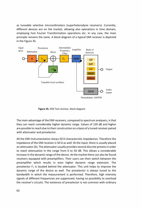
62
as tuneable selective microvoltmeters (superheterodyne receivers). Currently, different devices are on the market, allowing also operations in time domain, employing Fast Fourier Transformation operations etc. In any case, the main principle remains the same. A block diagram of a typical EMI receiver is depicted in the Figure 35.
The main advantage of the EMI receivers, compared to spectrum analysers, is that they can reach considerably higher dynamic range. Values of 120 dB and higher are possible to reach due to their construction on a basis of a tuned receiver paired with attenuator and preselector.
All the EMI instrumentation shows 50 Ω characteristic impedances. Therefore the impedance of the EMI receiver is 50 Ω as well. At the input, there is usually placed an attenuator (A). The attenuator usually provides several discrete presets in order to reach attenuation in the range from 0 to 50 dB. This allows a considerable increase in the dynamic range of the device. At the market there can also be found receivers equipped with preamplifiers. Their users can then switch between the preamplifier which results in even higher dynamic range extension. The preselector F1 is located behind the attenuator. This unit helps to improve the dynamic range of the device as well. The preselector is always tuned to the bandwidth in which the measurement is performed. Therefore, high intensity signals of different frequencies are suppressed, having no possibility to overload the receiver’s circuits. The existence of preselector is not common with ordinary
A F1
LO
F2 AMP
DEM
QP MP
AV RMS
other
Input 50 Ω Attenuator
Preselector Mixer
Intermediate Frequency
Filter Amplifier
Bank of detectors
Output
Audio output
Demodulator AM/FM
Tuneable local oscillator
Figure 35. EMI Test receiver, block diagram
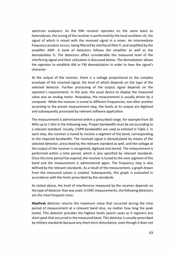
63
spectrum analysers. As the EMI receiver operates on the same basis as heterodynes, the tuning of the receiver is performed by the local oscillator LO, the signal of which is mixed with the received signal in a mixer. An intermediate frequency product occurs, being filtered by interfacial filter F2 and amplified by the amplifier AMP. A bank of detectors follows the amplifier as well as the demodulator D. The detectors affect considerably the measured level of the interfering signal and their utilization is discussed below. The demodulator allows the operator to establish AM or FM demodulation in order to hear the signal’s character.
At the output of the receiver, there is a voltage proportional to the complex envelope of the received signal, the level of which depends on the type of the selected detector. Further processing of the output signal depends on the operator’s requirements. In the past, the usual device to display the measured value was an analog meter. Nowadays, the measurement is usually driven by a computer. While the receiver is tuned to different frequencies, one after another according to the preset measurement step, the levels at its output are digitized and subsequently processed by relevant software application.
The measurement is administered within a prescribed range, for example from 30 MHz up to 1 GHz in the following way. Proper bandwidth must be set according to a relevant standard. Usually, CISPR bandwidths are used as enlisted in Table 1. In each step, the receiver is tuned to receive a segment of the band, corresponding to the required bandwidth. The received signal is demodulated by means of the selected detector, prescribed by the relevant standard as well, and the voltage at the output of the receiver is recognized, digitized and stored. The measurement is performed within a time period, which is also specified by relevant standards. Once this time period has expired, the receiver is tuned to the next segment of the band and the measurement is administered again. The frequency step is also defined by the relevant standards. As a result of the measurement, a graph drawn from the measured values is created. Subsequently, this graph is evaluated in accordance with the limits prescribed by the standards.
As stated above, the level of interference measured by the receiver depends on the type of detector that was used. In EMC measurements, the following detectors are the most frequent ones:
MaxPeak detector returns the maximum value that occurred during the time period of measurement at a relevant band slice, no matter how long the peak lasted. This detector provides the highest levels (worst case) as it registers any short peak that occurred in the measured band. This detector is usually prescribed by military standards because any short-term disturbance, even though it does not
64
carry enough energy to create harmful interferences, can reveal the masked unit when detected.
Average detector returns the average value of the measured signal’s level. If the signal is stationary, i.e. its level does not vary in time, the output of the average detector will be the same as the output of the MaxPeak detector. On the other hand, in most cases, short term peaks occur while the average level of interferences is lower. In these cases the values obtained by the Average detector are lower. In other words, the average detector ignores the peaks occurring at short periods. The comparison of levels obtained by this detector and the MaxPeak detector will provide an idea of how the measured interference varies in time. This detector is usually used when conducted emissions are measured.
QuasiPeak detector provides results that always lay between the results obtained by the MaxPeak and the Average detectors. Its output voltage is proportional to the voltage-time area of the envelope of the input inter-frequency signal and is thus influenced by both the magnitude and the repetition frequency of the input pulses of the interfering voltage. In other words, if the measured signal is stationary (no changes occurring in its level and frequency), it provides the same values as the MaxPeak detector as well as the Average detector. On the other hand, if the interfering signal consists of a stationary component as well as of the short-period peaks, the output of the QuasiPeak detector will be between the outputs of the Average and the MaxPeak detectors and it will be closer to the results of the MaxPeak detector if the number of the peaks is high, and vice versa, it will be closer to the Average detector’s output, if the number of the peaks occurring in the interfering signal is negligible. The QuasiPeak detector is prescribed by many standards as it provides more accurate information on how harmful the measured interference is. The following analogy can roughly be applied: if there is one acoustic pulse occurring in silence, it is perceived as less disturbing than if there are more such pulses in a period of time. Even though the QuasiPeak detector provides relevant information on how much the interfering signal disturbs, its utilization brings a considerable disadvantage. This is because it takes a very long time to measure. In order to ensure measurement repeatability, the time constants of integration members of the QuasiPeak detector are standardized and they are quite large. Therefore, the measurement using QuasiPeak detector may take hours while the same measurement using MaxPeak or Average detector takes tens of minutes. For this reason, many labs introduced the following solution: At first, the measurement is done with the MaxPeak detector, even though the QuasiPeak detector has been prescribed by the relevant standard. In comparison with the QuasiPeak detector, the MaxPeak detector provides higher or equal values, it can be stated that when the limit

65
requirements are fulfilled with values obtained by means of the MaxPeak detector, they will be fulfilled with the values obtained by means of the QuasiPeak detector as well. Subsequently, if at any frequency the prescribed limit is exceeded, the second measurement with QuasiPeak detector is performed, but only within the boundaries of the suspicious frequency. This approach considerably saves time and money of the EMC labs’ customers.
Usually, the EMI receivers are equipped with many more types of detectors, for example the Root-Mean Square detector (RMS), MinPeak detector and others. These detectors are useful when performing research and development of any device, but they are usually not required by the standards.
CISPR band Frequency range Filter bandwidth A 9 – 150 kHz 200 Hz B 150 kHz – 30 MHz 9 kHz C 30 MHz – 300 MHz 200 kHz D 300 MHz – 1 GHz 200 kHz E > 1 GHz 1 MHz
In order to achieve the correct measurement results, not only the proper detector must be used, but the proper bandwidth must be set as well. In the Table 1, the most frequent CISPR bandwidths are enlisted. Not only the selection of the proper
Time
Level MaxPeak detector
MinPeak detector
Average detector QuasiPeak detector
Figure 36. If the level of the interferences varies in time, different detectors provide different results
Table 1. IF filter bandwidths prescribed by CISPR 16.

66
detector affects the level of the measured interference, but the setting of the proper bandwidth does it as well. It should be remembered, that the EMI receiver obtains the output level by integration over the received bandwidth. The wider the bandwidth is, the higher the level of interference is measured. This is evident especially with wideband signals that have a rich spectrum. This situation is depicted in the Figure 37. For completeness, let’s note that the bandwidth of the IF filter is given for a decrease of 6 dB in EMI receivers unlike the usual value of 3 dB commonly used in electronics.
Based on the above mentioned, in order to achieve valid results, the operator of the EMI receiver must properly set the following:
• intermediate frequency filter bandwidth, • frequency step, • length of measurement at each of the frequency steps, • detector type.
The prescribed settings are defined in relevant standards. Depending on the intensity of the measured signal, appropriate setting of attenuator or preamplifier may also be required. The dynamic range of the EMI receiver is limited by two factors. The lowest measurable value is given by the noise of the device while the highest measurable value is given by the maximum signal level the device is able to process without any distortion. Usually, it is convenient to operate the EMI receiver in the higher half of its dynamic range where its own noise is negligible. The proper setting of the device is based on the operator’s experience. There are
Frequency Time
Level Meter output
Narrow filter bandwidth
Wide filter bandwidth
Figure 37. Illustration on how the filter bandwidth affects the measured level in case of broadband interferences. While the narrow filter enables the meter to recognize only one spectral line, wide filter will let more spectral lines be measured, resulting in higher output level of the meter.

67
also certain EMI receivers that can automatically switch the preamplifier or attenuator on and off.
As stated above, for some measurements, spectrum analysers may also be used. They are usually much faster when displaying the measured spectrum, but on the other hand they suffer from lower achievable dynamic range and they do not provide results corresponding to the above mentioned detectors. At present, there are several hybrid devices on the market that can operate not only as a spectrum analyser but also as EMI receiver. Very often they employ Discrete Fourier Transformation and other computational algorithms in order to reach the same results as the generic EMI receiver would give, but in a considerably shorter time. These devices may be used for EMI measurements provided they are compliant with the requirements given by CISPR 16 standard.
In his laboratory practice, the author of this book also uses oscilloscope together with near-field probes. Such a measurement has no support in standards. On the other hand, if the tested device generates higher interferences than allowed, the near-field probes are ideal to find the point of origin of the interference. Furthermore, when the interference is displayed as a waveform in time domain on the display of the oscilloscope, it is sometimes easier to find out what kind of signal it is (clock signals, power pulses, etc.).
Figure 38. EMI test receiver

68
5.6.2 Interference generators As stated in the chapter 3.3, a large number of different immunity tests exist. Usually, these tests require specific devices that can generate the correct test signals. The most common devices are described within this subchapter.
The standard IEC 61000-4-2 describes the electrostatic discharge immunity test. Such a test simulates electrostatic discharge that may occur when the operator touches the tested device by his hand. Human body is capable of handling charges as high as several µC. Because the typical capacity of a human body is around 150 pF, the corresponding voltage is between 2 and 16 kV. The ESD test generator consists of a high voltage source that charges a capacitor with a capacitance normalized to 150 pF. The charge at this capacitor is then discharged through a resistor the resistance of which is approximately 330 Ω to a tested device. The resistor limits the discharge current, simulating the impedance of the human skin. The ESD test generator is depicted in the Figure 40. It uses two types of heads. One head is equipped with a round tip that allows to accumulate enough charge to establish air discharge between the test generator and the test device. The second head is equipped with a sharp tip that enables to establish a direct discharge due to contact of the test generator with the tested device.
Another widely applied standard IEC 61000-4-3 describes the test of immunity against radiated electromagnetic field. The tested device is placed inside the
Figure 39. Oscilloscope with a near field probe

69
shielded room together with a transmitting antenna and homogenous electromagnetic field (see chapter 6.2) is generated. The antenna is driven by means of radio-frequency power amplifiers, the achievable output power of which is usually in hundreds or thousands of watts. The test waveform is generated by suitable EMS test generator. Most tests are performed in the range from tens of MHz up to ones of GHz and the test signal is usually modulated. Different modulations may be prescribed by the relevant standards. However, the most widely applied is the 80% amplitude modulation using the modulation frequency of 1 kHz. The level of the generated electromagnetic field inside the shielded room is monitored by a field probe. The field probe may be used as a feedback loop according to which the testing level is set, or it may be used to calibrate the exact level of the field in different points of an irradiated area. In the second case, the appropriate level for each of the tested frequency is stored in a calibration file and the probe is used only for monitoring of the field inside the room while the appropriate level of the electromagnetic field is set according to the calibration file.
Figure 40. Portable ESD test generator Haeffely
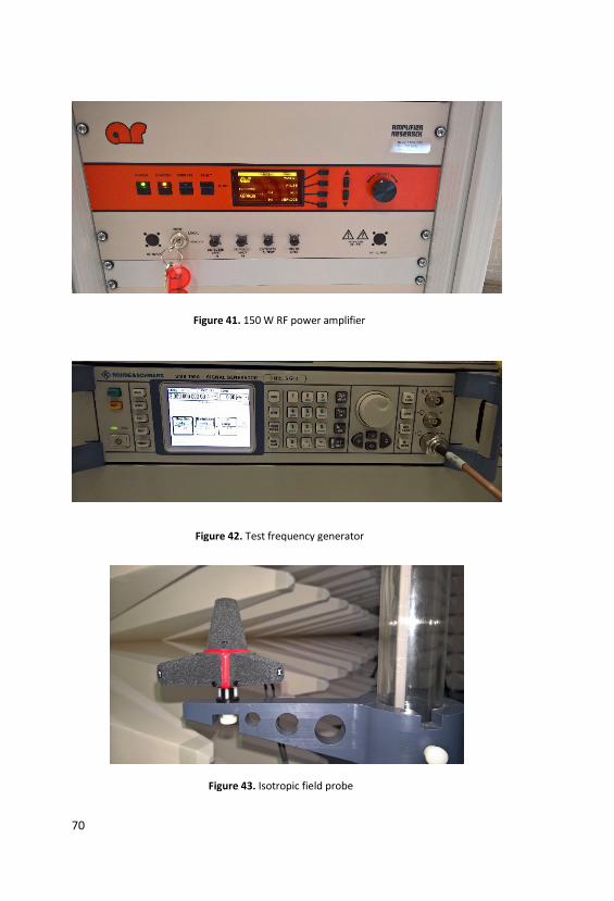
70
Figure 41. 150 W RF power amplifier
Figure 42. Test frequency generator
Figure 43. Isotropic field probe
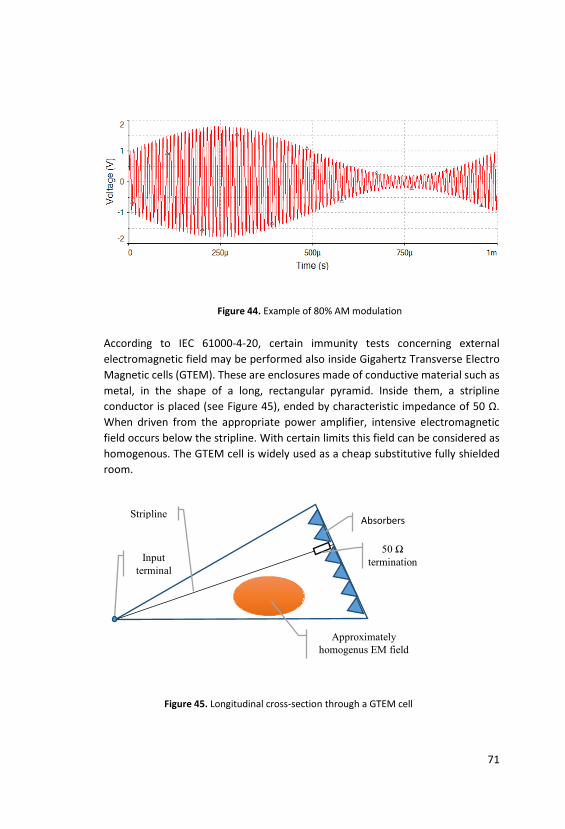
71
According to IEC 61000-4-20, certain immunity tests concerning external electromagnetic field may be performed also inside Gigahertz Transverse Electro Magnetic cells (GTEM). These are enclosures made of conductive material such as metal, in the shape of a long, rectangular pyramid. Inside them, a stripline conductor is placed (see Figure 45), ended by characteristic impedance of 50 Ω. When driven from the appropriate power amplifier, intensive electromagnetic field occurs below the stripline. With certain limits this field can be considered as homogenous. The GTEM cell is widely used as a cheap substitutive fully shielded room.
Absorbers
50 Ω termination
Stripline
Input terminal
Approximately homogenus EM field
Figure 44. Example of 80% AM modulation
Figure 45. Longitudinal cross-section through a GTEM cell

72
Susceptibility tests according to the standards IEC 61000-4-4: electrical fast transient / burst immunity test and IEC 61000-4-5: surge immunity test require special generator that is connected between the tested device and the power supply network. This generator delivers the standard power supply to the tested device and in addition it admixes the interfering pulses in it. Such a generator usually supports other susceptibility tests, for example magnetic field test or power supply voltage dips, ripples etc. The manufacturers of the devices declare what tests they are capable to perform. The application of such devices is quite easy. The user selects the test he wants to perform in the generator’s menu and confirms the setting of peak voltages, time constants etc. Most devices allow to modify parameters of the generated interferences. However, as these parameters are prescribed by relevant standards, it is usually sufficient to select the relevant standard in the menu of the generator. An example of such generator is depicted in the Figure 47.
Figure 46. GTEM cell

73
It is worth noting that not all the IEC tests enlisted in the chapter 3.3 are required for a certification of a device. A large number of specific tests are applicable only in specific devices. Different equipment may be required to perform these tests. Therefore only the most frequently used devices are described in this chapter.
5.6.3 Antennas Antennas belong to the necessary equipment of each EMC laboratory. The antenna is the interface between radio waves propagating through space and electric currents moving in metal conductors, together with a transmitter or receiver. If not equipped with additional units as preamplifiers etc., all of them may be operated in both the transmitter or receiver mode. Although different antenna constructions are known, only a few kinds of antennas are used in EMC labs. These antennas were found to be most convenient for the purposes of measurement or testing radio frequency field generating.
With the exception of geometric layout and dimensions, the following parameters are the most important:
Characteristic impedance of the antenna should be 50 Ω in order that the impedance matching criteria were fulfilled. Also the antenna cables have the impedance of 50 Ω and the receiver inputs as well as the amplifier outputs are also matched to the impedance of 50 Ω. Using the standardized impedance, reflections
Figure 47. EMS Test generator

74
on the connections between the antenna and the cable and between the cable and the connected device are minimized. These reflections could spoil the measurement completely.
The antenna factor is a frequency-dependent variable that must be measured and declared with each of the antenna used in the EMC laboratory. The antenna’s manufacturer declares this value by means of a calibration protocol. According to physical principles, the antenna cannot convert the received electromagnetic field to the voltage at its terminals with no losses and vice versa, it does not transmit all the energy delivered from the power amplifier, not even evenly in space. When operated in receiving mode, the antenna factor says how much the voltage at the antenna’s terminals must be amplified in order that it corresponded with the level of the electromagnetic field that approached the antenna. For example, the receiver indicates that at the frequency of 100 MHz, the voltage at the terminals of the antenna is 100 µV which corresponds to the level of 40 dBµV. However, this is not a relevant value, because the manufacturer of the antenna declares that the antenna factor of the antenna at the frequency of 100 MHz is AF(100) = 15.4 dB. In fact, the field intensity is 40 + 15.4 = 55.4 dBµV/m (i.e. approximately 0.6 mV/m).
The antenna gain exists as a result of the fact that no antenna acts as an isotropic transmitter or receiver. Due to their geometry, the antennas are always more sensitive in some directions while in other directions they are sometimes almost unusable. In practice, directional and omni-directional antennas are used. In case of directional antennas, the construction is performed in a way so that the antenna is as much sensitive as possible in one direction in exchange for being miserable in other directions. The omni-directional antennas are constructed in a way so they are not sensitive to their orientation too much, at least in one of the planes. However, no strictly isotropic antenna exists. The antenna gain is usually expressed in dB. It says how much more energy the antenna transmits in the direction of its main transmitting lobe compared to the theoretically ideal anisotropic transmitting antenna. In fact, there is no gain in terms of amplification of the output power. The power delivered to the antenna is only directed in a certain direction while the power transmitted to other directions is proportionally lower. Concerning the professional antennas, usually the radiation patterns are included in the documentation. An example of an antenna’s radiation pattern is depicted in the Figure 48.

75
The transmitting antennas should also sustain considerable continuous transmitting power. According to the amplifier, this power can be in hundreds or thousands of watts. In the Figure 49 there is an example of a transmitting antenna HL 046E by Rohde & Schwarz. It can be operated at the frequencies from 80 MHz up to 3 GHz with the power as high as 1 400 W at 80 MHz and 250 W at 3 GHz. As it covers the whole frequency range of the susceptibility test according to IEC 61000-4-3, it is suitable for susceptibility tests with the electric field intensity up to 30 V/m at a distance of 3 meters. It is worth noting that any directional antenna that sustains the transmitting power and covers the required frequency range can be used for susceptibility test according to EN 61000-4-3.
Figure 48. A typical antenna radiation pattern. The gain is the ratio between the field intensity generated in the direction of 0° compared to the performance of an ideal isotropic transmitter.
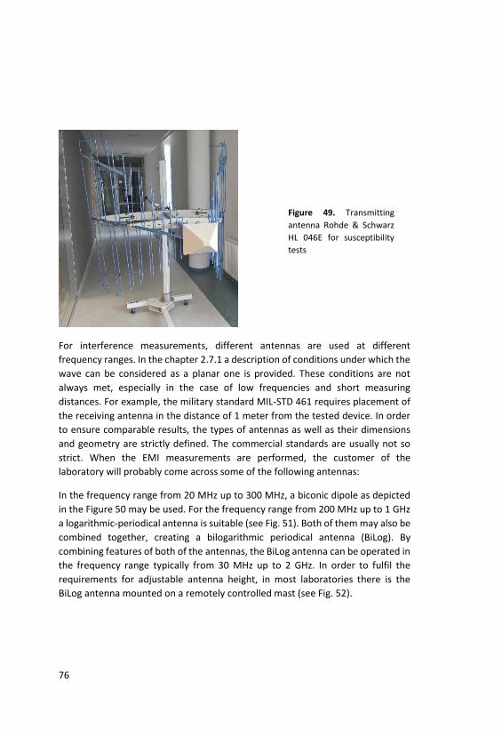
76
For interference measurements, different antennas are used at different frequency ranges. In the chapter 2.7.1 a description of conditions under which the wave can be considered as a planar one is provided. These conditions are not always met, especially in the case of low frequencies and short measuring distances. For example, the military standard MIL-STD 461 requires placement of the receiving antenna in the distance of 1 meter from the tested device. In order to ensure comparable results, the types of antennas as well as their dimensions and geometry are strictly defined. The commercial standards are usually not so strict. When the EMI measurements are performed, the customer of the laboratory will probably come across some of the following antennas:
In the frequency range from 20 MHz up to 300 MHz, a biconic dipole as depicted in the Figure 50 may be used. For the frequency range from 200 MHz up to 1 GHz a logarithmic-periodical antenna is suitable (see Fig. 51). Both of them may also be combined together, creating a bilogarithmic periodical antenna (BiLog). By combining features of both of the antennas, the BiLog antenna can be operated in the frequency range typically from 30 MHz up to 2 GHz. In order to fulfil the requirements for adjustable antenna height, in most laboratories there is the BiLog antenna mounted on a remotely controlled mast (see Fig. 52).
Figure 49. Transmitting antenna Rohde & Schwarz HL 046E for susceptibility tests

77
Figure 50. Biconical antenna with optimized antenna factor
Figure 51. Logarithmical periodic antenna

78
At the frequencies higher than 1 GHz, the most suitable antenna is the double ridged horn as depicted in the Figure 53. Different horns are placed on the market, varying in the utilizable frequency range. For example, the HL 906 antenna shown in the Figure 53 can be operated in the frequency range from 1 GHz up to 16 GHz. For higher frequencies, the antennas are proportionally smaller.
Figure 52. BiLog antenna Teseq CBL 6112 mounted on an adjustable mast

79
Figure 53. Double ridged horn antenna Rohde & Schwarz HF 906
Figure 54. Monopole with preamplifier

80
5.6.4 Near field probes The radiated emissions should be measured from such a distance at which the electromagnetic field can be considered as the far field (the transmitter and the receiving antenna are far from each other so that both of them may be considered as points in the space). In most cases, when the measurement with antennas is performed, this requirement is fulfilled. Except for these measurements, that are well known and standardized, there is also a possibility to monitor the electric or magnetic component of the field in the immediate vicinity to the tested device. Although such a measurement has no support in the standards because the physical conditions are impossible to describe (unlike the measurements in the far field), there are sets of near field probes for the purposes of indicative measurements. The near field probes are usually not too sensitive, but they are still useful when locating the source of the interferences. A set of near field probes is depicted in the Figure 56.
Figure 55. Frame antenna sensitive to magnetic field

81
The application of the near field probes is easy. They are usually paired together with a preamplifier, because their sensitivity is low. The output of the preamplifier can be connected to the oscilloscope or the spectrum analyser. The EMI receiver is not particularly suitable for monitoring of the measured signal because its response is slow. The operator moves the probe in the vicinity of the device under test, changes its direction and observes the output at the display of the monitoring device. In this way, it is possible to locate precisely the source of the interference.
As the equation (34) is not valid in the near field, the operator should check whether better results are obtained with the electric field probe or with the magnetic field probe. Generally speaking, big changes in voltage generate more of an electrical field while big changes in current generate more of a magnetic field. Realizing this will allow us to determine the source of the interference even better.
5.6.5 Tools for measurement of conducted interferences Generally, the conducted interferences are those ones that spread by means of power supply cables, data cables, etc. There are generally two ways how to perform their measurement:
1. A current probe is mounted as a closed loop around the tested wire. The interfering current passing through the wire will induce voltage in the
Figure 56. A set of near field probes
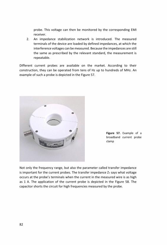
82
probe. This voltage can then be monitored by the corresponding EMI receiver.
2. An impedance stabilization network is introduced. The measured terminals of the device are loaded by defined impedances, at which the interference voltages can be measured. Because the impedances are still the same as prescribed by the relevant standard, the measurement is repeatable.
Different current probes are available on the market. According to their construction, they can be operated from tens of Hz up to hundreds of MHz. An example of such a probe is depicted in the Figure 57.
Not only the frequency range, but also the parameter called transfer impedance is important for the current probes. The transfer impedance ZT says what voltage occurs at the probe’s terminals when the current in the measured wire is as high as 1 A. The application of the current probe is depicted in the Figure 58. The capacitor shorts the circuit for high frequencies measured by the probe.
Figure 57. Example of a broadband current probe clamp

83
𝑍𝑍𝑇𝑇 =𝑈𝑈𝑇𝑇𝐼𝐼𝐶𝐶
[Ω] (53)
Where UT is the voltage measured at the terminals of the probe while IC is the current passing through the measured conductor. The transfer impedance is frequency dependent and its typical course is depicted in the Figure 59.
The transfer impedance enables a simple conversion between the current in expressed in dBµA and the voltage expressed in dBµV:
𝑍𝑍𝑇𝑇[𝑔𝑔𝐵𝐵Ω] = 𝑈𝑈[𝑔𝑔𝐵𝐵𝜇𝜇𝑉𝑉] − 𝐼𝐼[𝑔𝑔𝐵𝐵𝜇𝜇𝐴𝐴] (54)
For completeness, let us mention injection probes that enable inducing of interferences into selected conductors only. They are necessary to perform
EuT Power source
EMI receiver
Current probe clamp
IC
UT
ZT
Frequency
ZT NOM
Figure 58. Current probe application
Figure 59. Typical frequency dependence of the current probe’s transfer impedance. ZT NOM is the nominal value.

84
conducted susceptibility tests and are usually combined together with the monitoring probes that act as a feedback device to determine the proper test level. The injection clamps are usually more bulky as they are fed directly from the power amplifiers and must sustain considerable RF power.
One of the most widely used devices in measurement of conducted emissions is the Line impedance stabilization network, abbreviated as LISN. The LISN is a set of filters that allows the power supply current to pass between the tested device and the power plug, while the interferences are not passed, but redirected to input of the EMI test receiver. From the impedance point of view, the standard CISPR 16-1 recognizes four basic constructions as depicted in the Figure 60.
The LISN a) is used for measurements in low voltage power supply networks in the frequency range from 9 kHz up to 30 MHz. In industrial power supply networks, the LISN b) is used. It can be operated at the frequencies from 150 kHz up to 30 MHz. The automotive industry employs the construction c), simulating the on-board power supply networks. The frequencies of operation lie in the range from 150 kHz up to 100 MHz. The type d) is, according to the standard CISPR 16, dedicated to “classical” power supply networks. In all cases, the 50 Ω resistor connected in parallel is in practice created by the input impedance of the EMI test receiver. As a rule of thumb, if the operator is not sure which LISN to utilize, he should connect the one that simulates the real operating conditions of the tested device’s power supply at most.
A block diagram of the LISN is depicted in the Figure 61. It is obvious that the LISN not only redirects the interferences generated by the Device under Test to the input of the EMI receiver, but it can serve as a power supply filter as well, blocking
50 µH
50 µH 5 µH
50 Ω 50 Ω 50 Ω
5 Ω 1 Ω
100 Ω
50 Ω
a) b) c) d)
Figure 60. Different types of LISN according to the purpose of their application (see text)
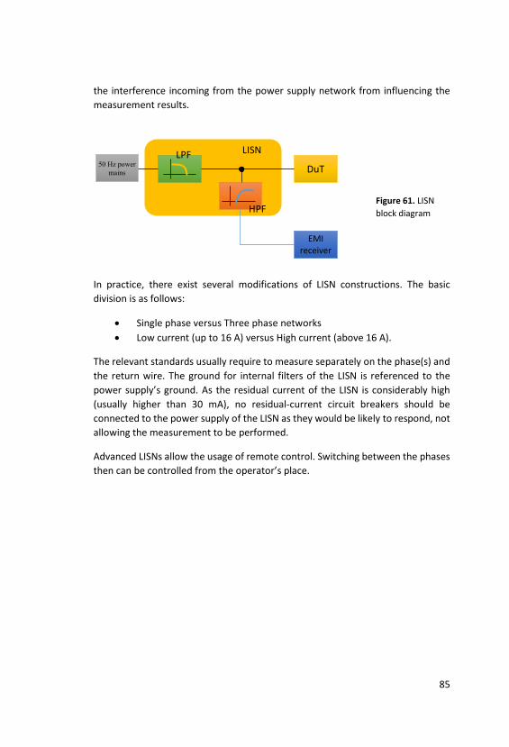
85
the interference incoming from the power supply network from influencing the measurement results.
In practice, there exist several modifications of LISN constructions. The basic division is as follows:
• Single phase versus Three phase networks • Low current (up to 16 A) versus High current (above 16 A).
The relevant standards usually require to measure separately on the phase(s) and the return wire. The ground for internal filters of the LISN is referenced to the power supply’s ground. As the residual current of the LISN is considerably high (usually higher than 30 mA), no residual-current circuit breakers should be connected to the power supply of the LISN as they would be likely to respond, not allowing the measurement to be performed.
Advanced LISNs allow the usage of remote control. Switching between the phases then can be controlled from the operator’s place.
DuT
EMI receiver
LISN LPF
HPF
50 Hz power
mains
Figure 61. LISN block diagram

86
Whilst the Line impedance stabilization networks allow the measurement of high frequency conducted emissions, network analysers are necessary to measure harmonics of power supply currents. With the increase of utilization of switched mode power supply sources and semiconductor rectifiers, the measurements with network analysers become important. While the resistive load (bulb, heater, etc.) sinks the current from the power supply network in phase with instantaneous voltage and proportionally to the voltage, the power supply units employing semiconductors usually sink current pulses that are correlated to the waveform of the voltage. However the spectrum of the current contains several harmonics. As a result, besides the main frequency of 50 Hz (60 Hz) there also occur frequencies of 100, 150, 200 etc. Hz (120, 180, 240, ….) respectively spreading across the power network. This situation is depicted in the Figure 63.
Figure 62. LISN Rohde & Schwarz
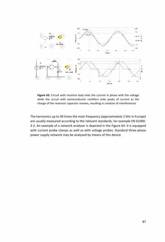
87
The harmonics up to 40 times the main frequency (approximately 2 kHz in Europe) are usually measured according to the relevant standards, for example EN 61000-3-2. An example of a network analyser is depicted in the Figure 64. It is equipped with current probe clamps as well as with voltage probes. Standard three-phase power supply network may be analysed by means of this device.
Figure 63. Circuit with resistive load sinks the current in phase with the voltage while the circuit with semiconductor rectifiers sinks peaks of current as the charge of the reservoir capacitor renews, resulting in creation of interferences
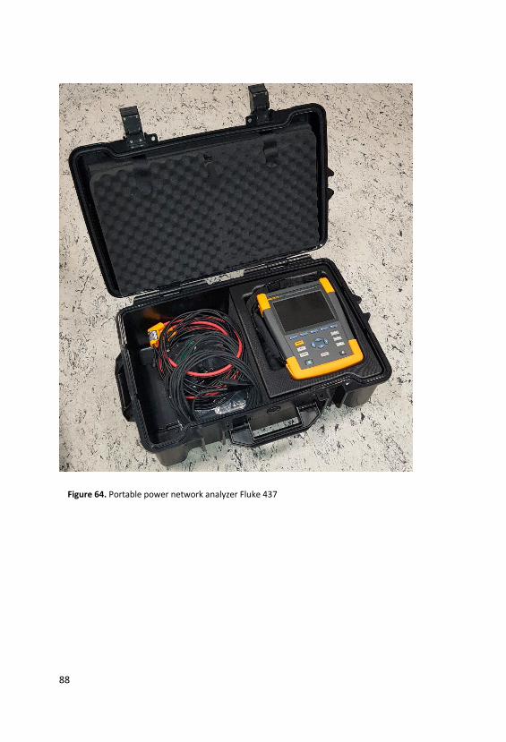
88
Figure 64. Portable power network analyzer Fluke 437

89
6 TESTS ON ELECTROMAGNETIC INTERFERENCES
Provided the Device under Test does not transmit any signal intentionally, there are not many test variants concerning its electromagnetic interferences. In substance, there are two basic tests to be performed:
• test on radiated interferences,• test on conducted interferences.
6.1 RADIATED INTERFERENCES OF COMMERCIAL DEVICES The radiated interferences are usually measured in several steps, according to the frequency ranges of the antenna used in the semianechoic room. In Europe, the generic standard for interference emissions is EN 61000-6-3. It specifies limits and frequency ranges that must be applied when no appropriate product standard is available. The EMC lab customer will probably meet one of the following product standards:
• EN 55011 (industrial, scientific and medical devices),• EN 55014 (household electric devices as drills, mixers etc.),• EN 55015 (lighting devices)• EN 55032 (multimedia devices).
Considering the above mentioned standards, the measurement of radiated electromagnetic emissions always starts at the frequency of 30 MHz. The upper frequency limit depends on the appropriate standard. For example, the standards EN 55014 or EN 55015 prescribe the highest measurement frequency as high as 300 MHz. The standard EN 55032 requires measurement up to the highest intentionally generated frequency multiplied by five or at least up to the frequency of 6 GHz, according of what comes first. In practice, BiLog antennas are usually used in the frequency range up to 1 GHz, together with the IF filter setting to 120 kHz (see Table 1). At the frequencies over 1 GHz, usually a horn antenna is used and the IF filter of the EMI receiver is switched to 1 MHz bandwidth. According to the relevant standards, different detectors are also usually employed at the frequencies above 1 GHz. While in the frequency range from 30 MHz up to 1 GHz the QuasiPeak detector must be used (see chapter 4.6.1), MaxPeak and Average detectors are used together at the frequencies higher than 1 GHz. The standards then prescribe limits for MaxPeak and Average detector separately and both of them must be met. When measuring at the frequencies higher than 1 GHz, there is another difference consisting in the fact that the room must be anechoic, i.e. there must be absorbers placed also on the floor of the room (see chapter 4.3).
https://doi.org/10.7441/978-80-7454-876-5_4
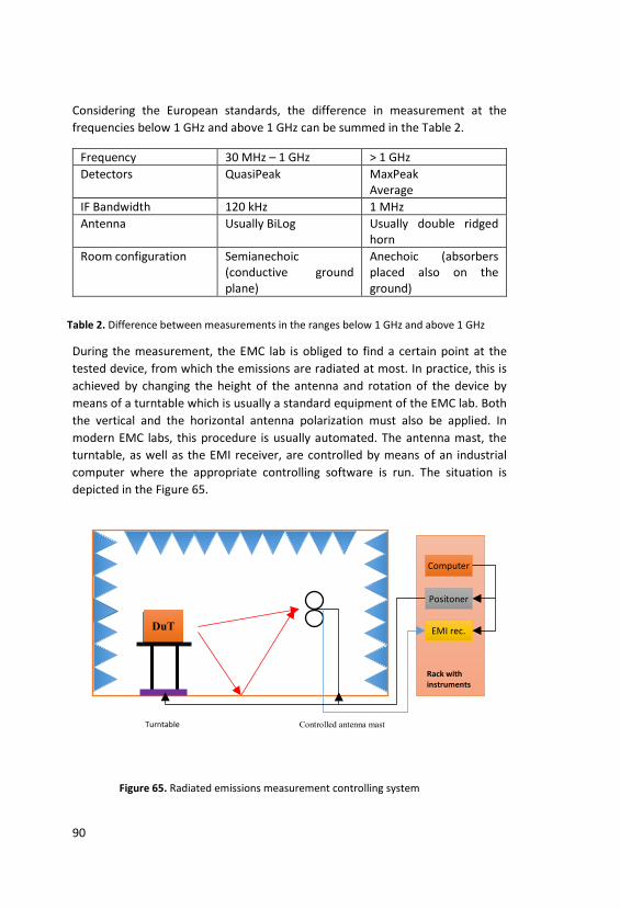
90
Considering the European standards, the difference in measurement at the frequencies below 1 GHz and above 1 GHz can be summed in the Table 2.
Frequency 30 MHz – 1 GHz > 1 GHz Detectors QuasiPeak MaxPeak
Average IF Bandwidth 120 kHz 1 MHz Antenna Usually BiLog Usually double ridged
horn Room configuration Semianechoic
(conductive ground plane)
Anechoic (absorbers placed also on the ground)
During the measurement, the EMC lab is obliged to find a certain point at the tested device, from which the emissions are radiated at most. In practice, this is achieved by changing the height of the antenna and rotation of the device by means of a turntable which is usually a standard equipment of the EMC lab. Both the vertical and the horizontal antenna polarization must also be applied. In modern EMC labs, this procedure is usually automated. The antenna mast, the turntable, as well as the EMI receiver, are controlled by means of an industrial computer where the appropriate controlling software is run. The situation is depicted in the Figure 65.
DuT
Rack with instruments
Computer
Positoner
EMI rec.
Turntable Controlled antenna mast
Table 2. Difference between measurements in the ranges below 1 GHz and above 1 GHz
Figure 65. Radiated emissions measurement controlling system

91
The typical situation according to Fig. 65 is as follows. The device is placed on the wooden table that is as high as 80 cm. This wooden table is mounted on a turntable that is integrated in the floor of the semianechoic room. The measuring antenna is placed in the distance of 3 or 10 m according to the dimensions of the room. The output terminals of the antenna are connected to the EMI receiver. The EMI receiver with the positioner that controls the turntable and the antenna mast are commanded by the computer. During the measurement, the relevant frequency range is scanned while the antenna is elevated and lowered and the turntable is rotated within the range from -180 up to 180 degrees. The measurement is done twice, firstly with the antenna in horizontal position and secondly, with the antenna in vertical position. The controlling software gathers the measurement data and evaluates the worst case situation. As a result, a table of critical frequencies is generated. According to the setting of the controlling software, it consists of a list of information including the following: frequencies at which the radiation is most intensive, what was the mutual antenna and turntable position when this result was acquired and whether the measured level is below or above the relevant limit.
Because the automated measurement consists of tens or hundreds of measurements (according to the software setting), employing of the QuasiPeak detector, as prescribed by most standards, would certainly affect the measurement time. Therefore, the usual approach to this measurement is as follows: at first, the operator of the EMI receiver tries to achieve as short measurement time as possible. Usually, MaxPeak detector is employed and mathematical signal analysis is on if supported by the receiver (see chapter 4.6.1 and the discussion on application of FFT algorithms). With this setting, the basic measurements are done and critical frequencies are found. Subsequently, the number of critical frequencies is limited to a convenient number. For example only 10 frequencies at which the emissions were the highest are selected. Subsequently, the accurate measurement is performed, using the receiver’s settings strictly following the appropriate standard. The accurate measurement is performed only in a narrow band around each of the critical frequencies and only for one antenna polarization and one mutual position of the antenna and the turntable (at which the emissions were the highest). The philosophy is simple – if at least at one frequency and in one situation the limits prescribed by the standards are exceeded, the device is not compliant with the standard and there is no need for further measurements. This approach allows the EMC lab operator to perform standardized test within a couple of hours.
For completeness, let us mention that there exist standards as EN 55032 or FCC 15 that distinguish between the indented applications of the tested devices. For

92
example, the FCC 15 distinguishes between devices marketed for use by the general public or intended to be used households and devices marketed for use in a commercial, industrial or business environment. The standard EN 55032 distinguishes between industrial (Class A) and other (Class B) devices. The Class A devices may reach up to 10 dB higher emissions compared to the Class B devices, but their susceptibility limits are also increased proportionally.
On the market, there are several software applications allowing automation of the measurement. In the Figure 66 there is an example of a screenshot of EMC 32 software delivered by Rohde & Schwarz.
6.2 CONDUCTED EMISSIONS OF COMMERCIAL DEVICES The following measurements usually belong to this category:
• high frequency measurements at power supply terminals. • high frequency measurements at data and communication terminals, • harmonic frequencies measurements at power supply terminals.
Figure 66. EMC 32 controlling software

93
The high frequency measurements at power supply terminals are measured by means of a suitable LISN (see chapter 4.6.5). Usually, the relevant standard requires that the measurement is performed on both the phase and the return conductor. The European generic standard EN 61000-6-3 and the extended product standards based on the former one usually require to perform the measurement in the frequency range from 150 kHz up to 30 MHz, using the Average and the QuasiPeak detectors. When measuring the radiated emissions, in order to achieve faster measurement, the QuasiPeak detector may be, under some circumstances, replaced by the MaxPeak detector. When the MaxPeak detector indicates that the Device under Test meets the requirements, the QuasiPeak detector will probably do so as well. Therefore, automated measurement systems combine MaxPeak detector for preliminary measurements and finally they use QuasiPeak detector only for final measurement at suspicious frequencies.
Configuration of the measuring workplace is defined by the standard CISPR 16. The Device under Test is placed on the wooden table together with the LISN. The distance between the DuT and the LISN is 80 cm. If the power supply cable is longer than 1 m, it must be meanderly folded between the LISN and the DuT. In case the DuT needs to be grounded for security reasons, the grounding conductor is connected to the appropriate terminal of the LISN. The LISN is grounded to the conductive ground plane. If no grounding of the DuT is required, the DuT must be placed 40 cm from artificial ground consisting of a vertical metal plate. The dimensions of the artificial ground metal plate must be at least 2 x 2 m and this must not be closer than 80 cm to any other metal piece that is not a part of the DuT.
As an alternative, indicative measurements of high frequency conducted emissions may be also performed with the aid of current probe clamps (see chapter 4.6.5). An example of results obtained by means of the current probe clamp and the controlling software EMC 32 is depicted at the end of this chapter.
Many standards as EN 55032 etc. prescribe also the measurement of conducted emissions occurring on data and communication terminals. A device similar to the LISN (see chapter 4.6.5) is applied and tuned to impedances and frequencies in the relevant measured paths. Generally, such a device is called Artificial network. During the measurement, the communication is run through the artificial network and the interferences are measured according to the pertinent standard.
At the power supply terminals, also the measurement of harmonics must be performed. Devices different from the high-frequency instruments are usually employed, for example the network analyser shown in the Figure 64. The device

94
is applied as depicted in the Figure 67. The Device under Test is connected to the power supply network. There are voltage and current probes connected to each of the power supply phases (the networks are either single-phase or three-phase). The voltage probes are usually constructed like a strap on contacts while the current probes are usually constructed like current probe clamps. This allows a connection of the analyser into the circuit without doing any arrangements and disconnecting of wires. In the Figure 68 there is an example on how the results of the measurement can look like.
DuT
Analyzer
L1
N
Current probe Voltage probes
Figure 67. Connection of power network analyzer to the Device under Test
Figure 68. Example of results obtained by the power network analyzer

95
0
10
20
30
40
50
60
70
80
90
100
110
120
10k 20 30 50 100k 200 300 500 1M 2M 3M 5M 10M 20 30M
Leve
l in d
BµA
Frequency in Hz
EN 50081_1_Pospisilik_Current QP
EN 50081_1_Pospisilik_Current AV
Figure 69. Example of a high frequency conducted emissions measured by a current probe clamp on a switching mode power supply source prototype
96
6.3 EMI TESTS ON OTHER THAN COMMERCIAL DEVICES There are certain sectors where different standards on electromagnetic compatibility tests are applied. The most known in this way are the military standards and automotive standards. The description of all differences from the “ordinary” commercial standards would exceed the range of this book, however, let us mention the most striking ones.
The military standards (in NATO, MIL 461 as amended is applied, but also STANAG and AECTP 500 in Europe) usually prescribe to perform all the measurements with the MaxPeak detector. Rather than the total amount of disturbing energy emitted into the space, emphasis is placed on the device not to leave any traces that could be caught by an enemy. Therefore the measurement of radiated emissions is done with the measurement distance of D = 1 m. According to the formula (3), the intensity of electric field is 10 times higher than when measured from the distance of 3 m. Despite that there is a limit on a group of devices including ground troop’s vehicles that prescribe the maximum level of interference as low as 27 dBµV/m if measured by MaxPeak detector. According to the theory, the short measurement distance causes results’ distortion, which is based on the fact that the antenna is operated in a near field of the measured device. For prevention purposes, the types, shapes and dimensions of antennas are strictly defined. Consequently, the measurement may not strictly uncover the physical reality, but it is repeatable in different laboratories around the world.
Different standards are also applied in the automotive sector and moreover car manufacturers usually define internal standards for their suppliers. These standards are usually stricter. This philosophy is supposed to ensure that when more different units produced by various suppliers are mounted in the final product (a car) the legally required standards are still met. There are two different cases that may occur. Firstly, the car may be measured as a whole, or only the single electronic devices are measured. In the second case, conditions inside the metal body of the car are simulated. The measured device is placed on a wooden table, but the wooden table is covered by a grounded metal plate and 50 mm distance between this ground and the device is ensured by underlaying of the device with non-conductive material with a low permittivity (usually polystyrene). The measurement is also performed at a short distance as in the case of the military standards. During the measurement, the device must be powered through the artificial network LISN, type c) (see Figure 60). The impedance of this LISN simulates the impedance of the connections between the accumulator of the vehicle and the measured device.

97
7 TESTS ON ELECTROMAGNETIC SUSCEPTIBILITY
Compared to the measurement of electromagnetic interferences, the tests on electromagnetic susceptibility are somewhat more varied. Complementary to the measurements described in Chapter 5, the testing of immunity to radio-frequency fields and conducted emissions are performed. However, as there are more mechanisms that may affect correct operation of the tested device, there is another group of tests performed with the aid of special generators. These tests simulate the electrostatic discharge, fast transients on conductors, magnetic field pulses etc. A complete list of tests distinguished by International Electrotechnical Commission can be found in the chapter 3.3.
One of the differences that may not be apparent at the first glance is that while in case of electromagnetic interferences the measurement is usually performed (we try to find the exact level of interference produced by the device), in case of electromagnetic susceptibility the functional tests are performed during actuation of standardized electromagnetic environment. The testing of DuT in controlled (calibrated) electromagnetic environment is a procedure different from measurement of EMI. The output of a test is not a value but a result from a set of possible cases. See chapter 3.4 for description of tests evaluation criteria.
Because there are many tests altogether, only the most frequent, prescribed by the standard EN 61000-6-1 are described here.
7.1 ELECTROSTATIC DISCHARGE IMMUNITY TEST Electrostatic discharge immunity test is one of the oldest EMC disciplines. It can even be argued that this issue has been dealt with long before the emergence of the field of electromagnetic compatibility as such (see chapter 3).
Table
DuT
ESD generator
2x 470 kΩ
Metal plate
Ground
Figure 70. ESD test workplace configuration
https://doi.org/10.7441/978-80-7454-876-5_5
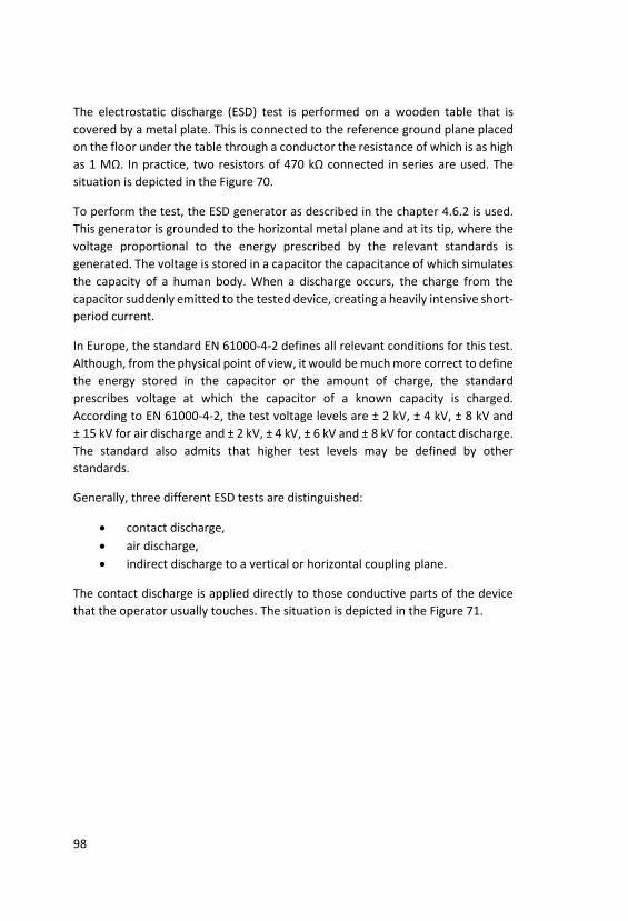
98
The electrostatic discharge (ESD) test is performed on a wooden table that is covered by a metal plate. This is connected to the reference ground plane placed on the floor under the table through a conductor the resistance of which is as high as 1 MΩ. In practice, two resistors of 470 kΩ connected in series are used. The situation is depicted in the Figure 70.
To perform the test, the ESD generator as described in the chapter 4.6.2 is used. This generator is grounded to the horizontal metal plane and at its tip, where the voltage proportional to the energy prescribed by the relevant standards is generated. The voltage is stored in a capacitor the capacitance of which simulates the capacity of a human body. When a discharge occurs, the charge from the capacitor suddenly emitted to the tested device, creating a heavily intensive short-period current.
In Europe, the standard EN 61000-4-2 defines all relevant conditions for this test. Although, from the physical point of view, it would be much more correct to define the energy stored in the capacitor or the amount of charge, the standard prescribes voltage at which the capacitor of a known capacity is charged. According to EN 61000-4-2, the test voltage levels are ± 2 kV, ± 4 kV, ± 8 kV and ± 15 kV for air discharge and ± 2 kV, ± 4 kV, ± 6 kV and ± 8 kV for contact discharge. The standard also admits that higher test levels may be defined by other standards.
Generally, three different ESD tests are distinguished:
• contact discharge, • air discharge, • indirect discharge to a vertical or horizontal coupling plane.
The contact discharge is applied directly to those conductive parts of the device that the operator usually touches. The situation is depicted in the Figure 71.
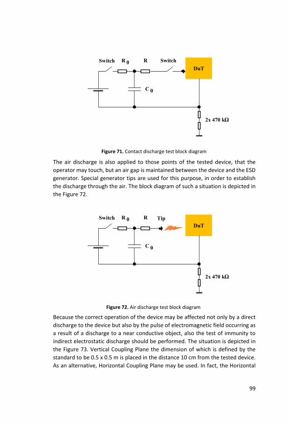
99
The air discharge is also applied to those points of the tested device, that the operator may touch, but an air gap is maintained between the device and the ESD generator. Special generator tips are used for this purpose, in order to establish the discharge through the air. The block diagram of such a situation is depicted in the Figure 72.
Because the correct operation of the device may be affected not only by a direct discharge to the device but also by the pulse of electromagnetic field occurring as a result of a discharge to a near conductive object, also the test of immunity to indirect electrostatic discharge should be performed. The situation is depicted in the Figure 73. Vertical Coupling Plane the dimension of which is defined by the standard to be 0.5 x 0.5 m is placed in the distance 10 cm from the tested device. As an alternative, Horizontal Coupling Plane may be used. In fact, the Horizontal
0 DuT
2x 470 kΩ
Switch R R
0 C
Switch
0 DuT
2x 470 kΩ
Switch R R
0 C
Tip
Figure 71. Contact discharge test block diagram
Figure 72. Air discharge test block diagram

100
Coupling Plane is the metal plate covering the table at the test site. At least 10 discharges should be applied at one position of the device and moreover, the device should be tested in such a way so all its sides are consequently oriented to the Coupling Plane.
7.2 RADIATED RADIO-FREQUENCY ELECTROMAGNETIC FIELD Together with the ESD test, this is also one of the tests of high importance, performed practically with almost all tested devices. The device is placed inside the anechoic room and it is irradiated by modulated electromagnetic field generated by a transmitting antenna. The situation is depicted in the Figure 74.
In Europe, the test is defined by the generic standard EN 61000-4-3. Frequency ranges and test levels are specified by the generic standards EN 61000-6-1 for household and commercial devices or EN 61000-6-2 for industrial devices. Generally, it can be said that the usual frequency range starts at 80 MHz and ends at 3 GHz and it can be covered by one antenna. The test levels are usually 3 V/m for household and commercial devices and 10 V/m for industrial devices. However, much higher levels may be required. For example, some manufacturers in the field of automotive industry require test levels up to 300 V/m.
According to our experience, when the test is performed in an ordinary anechoic room where the distance between the transmitted antenna and the tested device is 3 m, a power of approximately 150 W is needed to achieve the field intensity of 10 V/m without significant complications. For higher intensities, high frequency amplifiers with the power as high as thousands of watts are used. Alternatively, the GTEM cell can be used.
Table
DuT ESD
generator
2x 470 kΩ
Horizontal coupling plane
Ground
Insulating pad
Vertical coupling plane
2x 470 kΩ
Figure 73. Indirect discharge workplace configuration
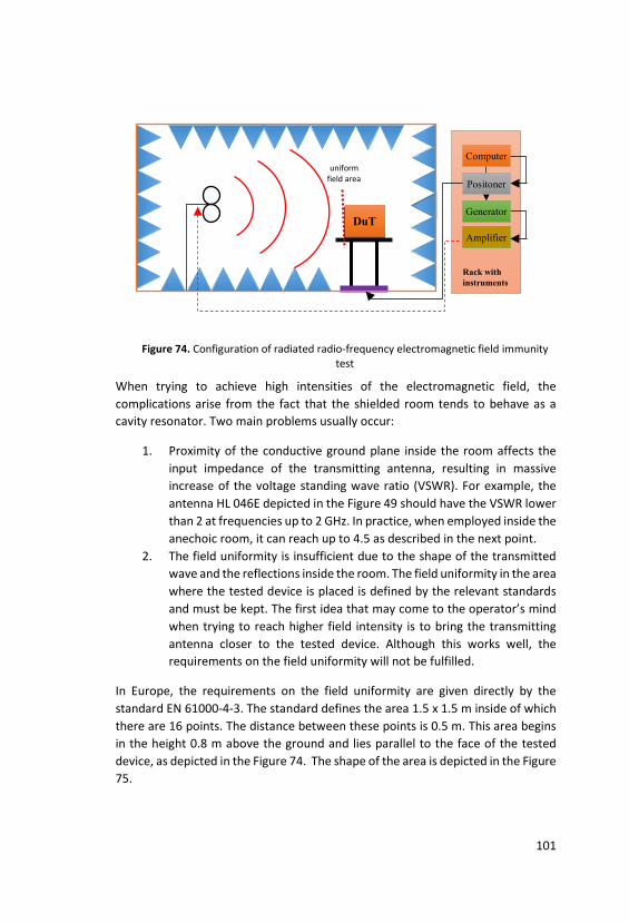
101
When trying to achieve high intensities of the electromagnetic field, the complications arise from the fact that the shielded room tends to behave as a cavity resonator. Two main problems usually occur:
1. Proximity of the conductive ground plane inside the room affects the input impedance of the transmitting antenna, resulting in massive increase of the voltage standing wave ratio (VSWR). For example, the antenna HL 046E depicted in the Figure 49 should have the VSWR lower than 2 at frequencies up to 2 GHz. In practice, when employed inside the anechoic room, it can reach up to 4.5 as described in the next point.
2. The field uniformity is insufficient due to the shape of the transmitted wave and the reflections inside the room. The field uniformity in the area where the tested device is placed is defined by the relevant standards and must be kept. The first idea that may come to the operator’s mind when trying to reach higher field intensity is to bring the transmitting antenna closer to the tested device. Although this works well, the requirements on the field uniformity will not be fulfilled.
In Europe, the requirements on the field uniformity are given directly by the standard EN 61000-4-3. The standard defines the area 1.5 x 1.5 m inside of which there are 16 points. The distance between these points is 0.5 m. This area begins in the height 0.8 m above the ground and lies parallel to the face of the tested device, as depicted in the Figure 74. The shape of the area is depicted in the Figure 75.
Rack with instruments
DuT
Computer Positoner
uniform field area
Generator Amplifier
Figure 74. Configuration of radiated radio-frequency electromagnetic field immunity test
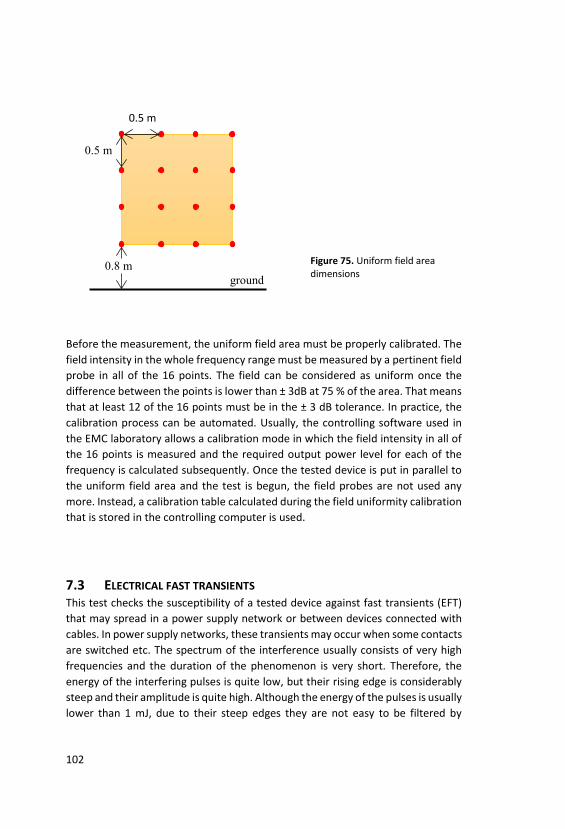
102
Before the measurement, the uniform field area must be properly calibrated. The field intensity in the whole frequency range must be measured by a pertinent field probe in all of the 16 points. The field can be considered as uniform once the difference between the points is lower than ± 3dB at 75 % of the area. That means that at least 12 of the 16 points must be in the ± 3 dB tolerance. In practice, the calibration process can be automated. Usually, the controlling software used in the EMC laboratory allows a calibration mode in which the field intensity in all of the 16 points is measured and the required output power level for each of the frequency is calculated subsequently. Once the tested device is put in parallel to the uniform field area and the test is begun, the field probes are not used any more. Instead, a calibration table calculated during the field uniformity calibration that is stored in the controlling computer is used.
7.3 ELECTRICAL FAST TRANSIENTS This test checks the susceptibility of a tested device against fast transients (EFT) that may spread in a power supply network or between devices connected with cables. In power supply networks, these transients may occur when some contacts are switched etc. The spectrum of the interference usually consists of very high frequencies and the duration of the phenomenon is very short. Therefore, the energy of the interfering pulses is quite low, but their rising edge is considerably steep and their amplitude is quite high. Although the energy of the pulses is usually lower than 1 mJ, due to their steep edges they are not easy to be filtered by
0.5 m
0.5 m
ground 0.8 m Figure 75. Uniform field area
dimensions
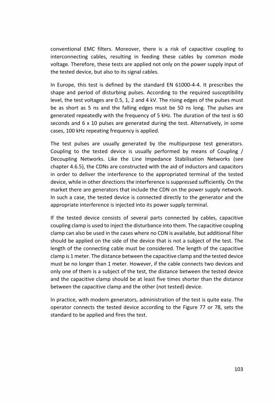
103
conventional EMC filters. Moreover, there is a risk of capacitive coupling to interconnecting cables, resulting in feeding these cables by common mode voltage. Therefore, these tests are applied not only on the power supply input of the tested device, but also to its signal cables.
In Europe, this test is defined by the standard EN 61000-4-4. It prescribes the shape and period of disturbing pulses. According to the required susceptibility level, the test voltages are 0.5, 1, 2 and 4 kV. The rising edges of the pulses must be as short as 5 ns and the falling edges must be 50 ns long. The pulses are generated repeatedly with the frequency of 5 kHz. The duration of the test is 60 seconds and 6 x 10 pulses are generated during the test. Alternatively, in some cases, 100 kHz repeating frequency is applied.
The test pulses are usually generated by the multipurpose test generators. Coupling to the tested device is usually performed by means of Coupling / Decoupling Networks. Like the Line Impedance Stabilisation Networks (see chapter 4.6.5), the CDNs are constructed with the aid of inductors and capacitors in order to deliver the interference to the appropriated terminal of the tested device, while in other directions the interference is suppressed sufficiently. On the market there are generators that include the CDN on the power supply network. In such a case, the tested device is connected directly to the generator and the appropriate interference is injected into its power supply terminal.
If the tested device consists of several parts connected by cables, capacitive coupling clamp is used to inject the disturbance into them. The capacitive coupling clamp can also be used in the cases where no CDN is available, but additional filter should be applied on the side of the device that is not a subject of the test. The length of the connecting cable must be considered. The length of the capacitive clamp is 1 meter. The distance between the capacitive clamp and the tested device must be no longer than 1 meter. However, if the cable connects two devices and only one of them is a subject of the test, the distance between the tested device and the capacitive clamp should be at least five times shorter than the distance between the capacitive clamp and the other (not tested) device.
In practice, with modern generators, administration of the test is quite easy. The operator connects the tested device according to the Figure 77 or 78, sets the standard to be applied and fires the test.
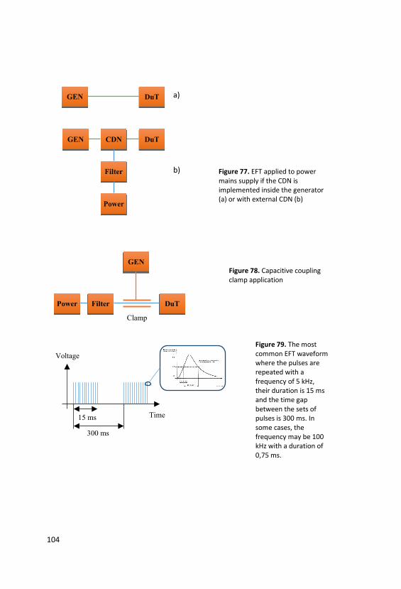
104
DuT GEN
DuT GEN CDN
Filter
Power
a)
b)
DuT
GEN
Filter Power Clamp
Time
Voltage
15 ms 300 ms
Figure 77. EFT applied to power mains supply if the CDN is implemented inside the generator (a) or with external CDN (b)
Figure 78. Capacitive coupling clamp application
Figure 79. The most common EFT waveform where the pulses are repeated with a frequency of 5 kHz, their duration is 15 ms and the time gap between the sets of pulses is 300 ms. In some cases, the frequency may be 100 kHz with a duration of 0,75 ms.
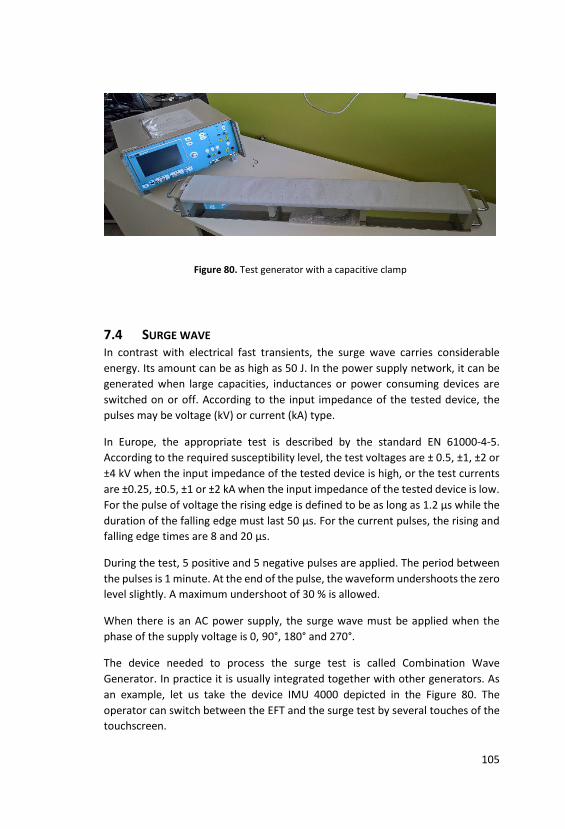
105
7.4 SURGE WAVE In contrast with electrical fast transients, the surge wave carries considerable energy. Its amount can be as high as 50 J. In the power supply network, it can be generated when large capacities, inductances or power consuming devices are switched on or off. According to the input impedance of the tested device, the pulses may be voltage (kV) or current (kA) type.
In Europe, the appropriate test is described by the standard EN 61000-4-5. According to the required susceptibility level, the test voltages are ± 0.5, ±1, ±2 or ±4 kV when the input impedance of the tested device is high, or the test currents are ±0.25, ±0.5, ±1 or ±2 kA when the input impedance of the tested device is low. For the pulse of voltage the rising edge is defined to be as long as 1.2 µs while the duration of the falling edge must last 50 µs. For the current pulses, the rising and falling edge times are 8 and 20 µs.
During the test, 5 positive and 5 negative pulses are applied. The period between the pulses is 1 minute. At the end of the pulse, the waveform undershoots the zero level slightly. A maximum undershoot of 30 % is allowed.
When there is an AC power supply, the surge wave must be applied when the phase of the supply voltage is 0, 90°, 180° and 270°.
The device needed to process the surge test is called Combination Wave Generator. In practice it is usually integrated together with other generators. As an example, let us take the device IMU 4000 depicted in the Figure 80. The operator can switch between the EFT and the surge test by several touches of the touchscreen.
Figure 80. Test generator with a capacitive clamp

106
For aircraft and military applications, also direct and indirect effects of lightning are concerned. The appropriate tests are defined by the standards EUROCAE ED-84B and EUROCAE ED-14G.
7.5 CONDUCTED RADIO-FREQUENCY INTERFERENCES If the device utilizes at least one conductive cable (power supply, ground, signal cables), its operation may be affected by induction of the energy transmitted by radio-frequency transmitters in its vicinity.
In Europe, there is a test defined by the standard EN 61000-4-6 that prescribes testing of the devices on conducted interferences in the frequency range from 150 kHz up to 80 MHz. According to the required immunity level, the voltages of the interferences may be 1, 3 or 10 V. As in the case of radiated interferences, amplitude modulation by the frequency of 1 kHz is applied. The modulation depth is 80 %. At each of the test frequencies, the dwell time must be at least 30 seconds.
To perform this test, a radio-frequencies’ generator with power amplifier is needed (see chapter 4.6.2). The injection of the interferences may be processed in three different ways:
• by means of a coupling / decoupling network (CDN), • by means of a capacitive clamp, • by means of a current clamp.
A typical setup using the current clamp is depicted in the Figure 81. For each of the frequencies, the level of the interference must be set according to the feedback measurement using an auxiliary clamp placed in the vicinity of the tested device.
DuT
GENERATOR AMPLIFIER
RECEIVER
Tested cable
Feedback
Figure 81. EN 61000-4-6 test setup with current clamps
107
7.6 POWER SUPPLY ERRORS During its operation, the device operated from the AC power network may also suffer from various malfunctions of the power supply. The most common disturbances, as well as the tests prescribed by the European standard EN 61000-4-11, are described below.
7.6.1 Voltage dips The power supply voltage slumps to a part of its nominal value for a time period of 20 ms and then rises back quite promptly to its nominal value.
According to the immunity level of the device, the test levels are 0, 40, 70 and 80 % of the nominal power supply voltage and the length of the test varies from 0.5 to 250 periods of the 50Hz power supply frequency or up to 300 periods if the power supply frequency is 60 Hz. The 0 % level is applied only for 0.5 or 1 period of the power supply voltage.
7.6.2 Short interruption The power supply voltage may also be interrupted completely at all power supply phases for a short period of time. After the interruption, the power supply delivery is restored. The maximum interruption time for the device of the highest immunity level is 1 minute.
7.6.3 Voltage sags In contrast to the above mentioned cases, the voltage sags are characterized by slow changes in the power supply voltage in consequence of changes in load of the power supply network.
During the test, the voltage is decreased quite rapidly to 70 % of the nominal level, then it is kept at this level for a short period of time, and, finally, it is slowly increased in order to reach the nominal level again.
7.6.4 Instrumentation In the past, these tests were administered by means of programmable autotransformers. However, combined generators are increasingly being used, as for example that one depicted in the Figure 80. The appropriate test is selected from the menu on the touchscreen and launched afterwards.
108
8 REFERENCES
[1] PAUL, C. R. Introduction to Electromagnetic Compatibility. John Wiley, New York 1992
[2] BOXLEITNER, W. Electrostatic Discharge and Electronic Equipment, IEEE Press, New York, 1989.
[3] SVAČINA, J. Electromagnetic Compatibility [Elektromagneticka kompatibilita], Brno: VUT Brno, 2002.
[4] GHOSE, R. N. Interference Mitigation – Theory and Application. IEEE Press, New York, 1996.
[5] CHATTERTON, P. A., HOULDEN, M. A. EMC – Electromagnetic Theory to Practical Design. John Wiley, New York, 1991.
[6] KEISER, B. Principles of Electromagnetic Compatibility. Artech House, Norwood, 1987.
[7] WHITE, D. R. J. A Handbook Series on Electromagnetic Interference and Compatibility. Don White Consultants, Germantown, Maryland 1971, 1973.
[8] TRNKA, Z. Theory of Electrical Engineering [Teoretická elektrotechnika]. SNTL Alfa, Bratislava, 1972.
[9] PAUL, C. R., NASAR, S. A., Introduction to Electromagnetic Fields, 2nd ed., McGraw-Hill, New York, 1987.
[10] PAUL, C. R., Electromagnetics for Engineers, Wiley, New York, 2004. [11] JORDAN, E. C., BALMAIN, K. G. Electromagnetic Waves and Radiating
Systems, 2nd ed., Prentice-Hall, Englewood Cliffs, NJ, 1968. [12] STUTZMAN, W. L., THIELE, G. A. Antenna Theory and Design, Wiley, New
York, 1981. [13] BALANIS, C. A., Antenna Theory Analysis and Design, Harper & Row, New
York, 1982.

109
9 ABBREVIATIONS
ACEC Advisory Committee on Electromagnetic Compatibility AV Average (detector) CDN Coupling/Decoupling Network CE Conformité Européenne CENELEC Comitté Européen de Normalisation en
Electrotechnique CISPR Comité International Spécial des Perturbations
Radioélectriques DuT Device under Test EFT Electrical Fast Transients EMC Electromagnetic Compatibility EMF Electromagnetic Field EMI Electromagnetic Interference EMS Electromagnetic Susceptibility ESD Electrostatic Discharge ETSI European Telecommunications Standards Institute EuT Equipment under Test FCC Federal Communications Commission (USA) FFT Fast Fourier Transformation GTEM Gigahertz Transverse Electro Magnetic (cell) IEC International Electrotechnical Commission ISO International Organization for Standardization ITE Information Technology Equipment ITU International Telecommunications Union LISN Line Impedance Stabilization Network MIL-STD Military Standard (NATO) MP Max Peak NSB National Standards Bodies OATS Open Area Test Site QP Quasi Peak RA Receiving Antenna RMS Root-Mean Square TA Transmitting Antenna TEM Transversal Electromagnetic VSWR Voltage Standing Wave Ratio
Introduction to Electromagnetic Compatibility for Electronic Engineers
… and not only for them
Ing. Martin Pospíšilík, Ph.D.
Published by Tomas Bata University in Zlín, nám. T. G. Masaryka 5555, 760 01 Zlín, Czech Republic, Reg. No. 70883521, in 2019. Cover design: Dušan Wolf, nakladatelstvi.utb.cz, freepik.com First edition. 110 pages. Format: A5. Impression: e-book ISBN 978-80-7454-876-5