Embed Size (px)
Citation preview

TNT2 HARDWARE DESCRIPTION TNT2 is a 4 Digitalisation Channels. It has been designed for Spectroscopy and other applications: The maximum sample Rates is 100 MHz (adjustable by soft) 14 bits. The anti-aliasing filter is around 50 MHz. The virtex2 is one of the fundamental components for all the board. All signals go through it. For a general point of view all the schematic design can be easily understood with the datasheet of the components. The block diagram is:
1

1. Analog Input signal:
The signal could be in differential mode or common mode. The selection is done by solder 0 Ohms resistance. The Common mode is design to work with an offset compensation. The Differential mode is design to work without offset compensation but is possible.
Differential mode
Common mode
50 Ohms
100 Ohms
2

Common mode
S6 S4 & S1 R6 R17 S5 50 Ohms
3

Common Mode example for Channel 1: S6 S5 SOLDER S4 S1 NOT SOLDER R6 = R17 = 1 K Ohms 1% Differential Mode example for Channel 1: S6 S5 NOT SOLDER S4 S1 SOLDER R6 NOT SOLDER R17 499 Ohms 1% 2. Logical Input/Output signals:
• Logical Input /Output Module
A block of 4 Logical Inputs signals and 4 Logical Output have been implemented on the board.
Logical Input Signals. The logical input signal can be positive (TTL) or negative (Nim) voltage. The input component AD8561 can be latch trough slow control interface to avoid no useful noise. The input impedance could be switch to 50 Ohms impedance trough the slow control interface. The adjustment of the voltage threshold is done with the potentiometer. Negatives Signals as Nim Input 1 P01 Input 2 P03 Input 3 P05 Input 4 P07 Positives Signals as TTL Input 1 P02 Input 2 P04 Input 3 P06 Input 4 P08
4

Electrical Schema P03 P04 P01 P02 Positive point measurement (pin3)
P05 P06 P07 P08 Negative point measurement (pin2) The logical input 1 and 2 are connecting to specific I/O of Virtex2. These input calls GCLCK are very useful for VHDL implementation. In the multiparameters mode every time than a signal appears to this input the Time sample associate is write on the data files. It’s very useful to control the synchronization with external event ( Beam; other Board ect )
5

Logical Output Signals. 4 Logical outputs are connecting on the front panel. The output signals are Nim level. Each output is connect as an OR electrical. If users want to suppress the OR connection the diode have to be not solder. The output current can be adjusted by resistor.
• Local Trigger Output Signals. These output signals are on the back panel, they are similar as the previous logical signals. But normally they are designated to be used as Local trigger for each channel. Users can use them as they want with VHDL modifications.
6

• LVDS bus interface.
The LVDS bus interface is dedicated to connect boards together. Two input signals are directly connect to Virtex2 GCK input. One could be used as Clock reference input coming from a master TNT2 board. In this case the global system will have one Clock. The other input signal can be use as a synchronisation clock. On the output bus one clock could be transfer to other board. Users can define how they want to use the bus with VHDL modifications.
7

3. Clock distribution TNT2 must have the capability to work in stand alone and/or with other TNT2 board. Because it have been design with the possibility to work in experimentation it’s possible to use different clock reference frequency. DDS chips from Analog device have been choice to monitor the Clock of the FADC. This component allows to user to choice the frequency work and allows a phase adjustment very useful in multiple board application.
The clock system can be dividing in two blocks.
The clock selector. The DDS
For more details see the AD9852 Data sheet
8

Clock reference distribution The clock reference input can be:
o Clock reference distribute by other TNT2 board trough the Virtex2 o Clock reference from Virtex2 Clock. o Clock input from front panel (LVTTL). o 20 MHz reference Oscillator o Clock from the Serdes but not implement for Commercial board.
Clock Output Bessel Filter 100 MHz Clock distributor
9
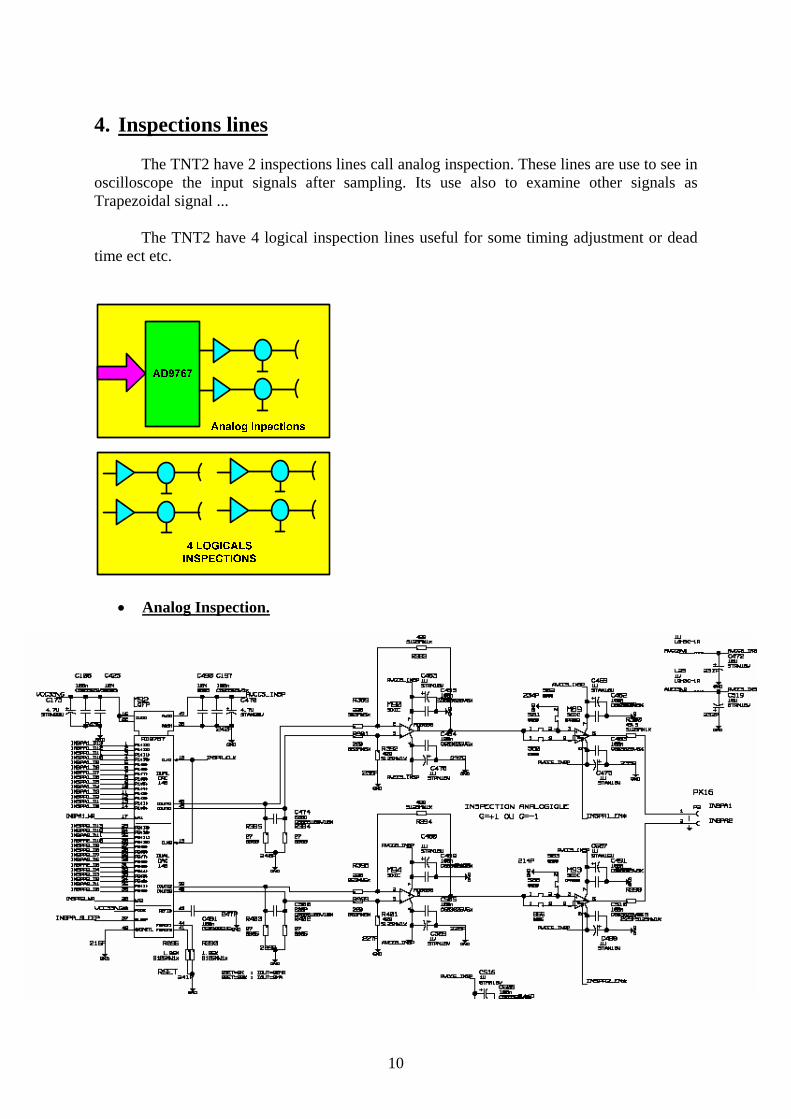
4. Inspections lines The TNT2 have 2 inspections lines call analog inspection. These lines are use to see in oscilloscope the input signals after sampling. Its use also to examine other signals as Trapezoidal signal ... The TNT2 have 4 logical inspection lines useful for some timing adjustment or dead time ect etc.
• Analog Inspection.
10

The analog inspection is done with a DAC from Analog Device 9767, 14 bits 150 MHz. The PCB is design for this component but to reduce the price we have solder in place the 9765, 12 bits 150 MHz completely enough for this type of application. The frequency is equal to the sample frequency for the ADC input.
• Logical inspection
The logical design is very simple. It consists to make a power interface from Virtex to the oscilloscope. It’s possible to change the gain by factor 2 if the 0 jumper is solder or not.
All the inspection lines can be commuted in high impedance through the soft interface to reduce power consumption.
11

5. Loader The TNT2 is design for versatile uses. All the functionalities depend of the VHDL code inside the VIRTEX2. Modify this program could be very useful depending of the physicist need. During the beginning of experiment some modifications are some time needed. But because the technical support cannot be in the experiment place, we have implemented the possibility than an engineer could modify the software. In this case the physicist will use the slow control interface to modify the virtex2 configuration. He’ll be not necessary to have a technical support every thing can be done at distance. The loader uses a Spartan2 as the interface loader. The default configuration is saving inside 3 EPROM (XF04S) which can be modifying trough specific interface from Xilinx. At each reboot the virtex2 start in this configuration. The new configuration is save in the EEPROM (AM29LV017D) and don’t need to be reload. Users just need to ask for a new configuration loading and to restart Soft interface.
12

6. SRAM Memory The TNT2 board can be used as an oscilloscope. The 4 channels are sampling in the same time. So 2 independents block memory exist. Each one has a bus of 64 bits. The memory use is an asynchronous memory 133 MHz, 512 K* 16 bits. The maximum capability is 1M Samples by channels.
A small block 32 bits 512 Word exists witch could be use as buffer output. In the actual implementation we use internal memory of the Virtex2 as a buffer.
13

Block memory 64 bits width on the Top 7. USB2 Interface The USB2 interface is done with a Cypress component. CY7C68013- FX2. A small EEprom have been installed with the component. This EEprom need to be program at the fist start with a specific number witch is the reference number of the board. The USB2 interface is use for
14