Embed Size (px)
Citation preview

TN-41-08: Design Guide for Two DDR3-1066 UDIMM SystemsIntroduction
Technical NoteDesign Guide for Two DDR3-1066 UDIMM Systems
IntroductionDDR3 memory systems are very similar to DDR2 memory systems. One noteworthy difference is the fly-by architecture used in DDR3 JEDEC-standard modules. Depending on the intended market for the finished product, the memory buses will vary, and the memory system support requirements will range from point-to-point topologies to large, multiple registered DIMM topologies.
This design guide is intended to assist board designers in developing and implementing their products. The document focuses on memory topologies requiring two unbuffered DIMM devices operating at a data rate of 1066 Mb/s and two variations of the address and command bus. The first design variation discussed is a system with one DIMM per copy of the address and command bus using 1T clocking. The second design variation is a system with two DIMM devices on the address and command bus using 2T clocking.
The first section of this technical note outlines a set of board design rules, providing a starting point for a board design. The second section details the calculation process for determining the portion of the total timing budget allotted to the board interconnect. The intent is that board designers will use the first section to develop a set of general rules and then, through simulation, verify their designs in the intended environment.
Fly-By ArchitectureDesigners who build systems using unbuffered DIMM devices can implement the address and command bus using various configurations. For example, some controllers have two copies of the address and command bus, so the system can have one or two DIMM devices per copy, but no more than two DIMM devices per channel. Further, the address bus can be clocked using 1T or 2T clocking. With 1T clocking, a new command can be issued on every clock cycle; 2T timing will hold the address and command bus valid for two clock cycles. This reduces the efficiency of the bus to one command per two clocks, but it substantially increases the amount of setup and hold time available for the address and command bus. The data bus remains the same for the address bus varia-tions.
DDR3 modules use faster clock speeds than earlier DDR technologies, making signal quality extremely important. For improved signal quality, the clock, control, command, and address buses have been routed in a fly-by topology, where each clock, control, command, and address pin on each DRAM is connected to a single trace and termi-nated. (Other topologies use a tree structure, where termination is off the module near the connector.) Inherent to fly-by topology, the timing skew between the clock and DQS signals can easily be accounted for using the write-leveling feature of DDR3.
PDF: 09005aef83a0af6b/Source: 09005aef83657fb2 Micron Technology, Inc., reserves the right to change products or specifications without notice.tn4108_ddr3_design_guide.fm - Rev. B 1/11 EN 1 ©2009 Micron Technology, Inc. All rights reserved.
Products and specifications discussed herein are for evaluation and reference purposes only and are subject to change by Micron without notice. Products are only warranted by Micron to meet Micron’s production data sheet specifications. All
information discussed herein is provided on an “as is” basis, without warranties of any kind.
TN-41-08: Design Guide for Two DDR3-1066 UDIMM SystemsFly-By Architecture
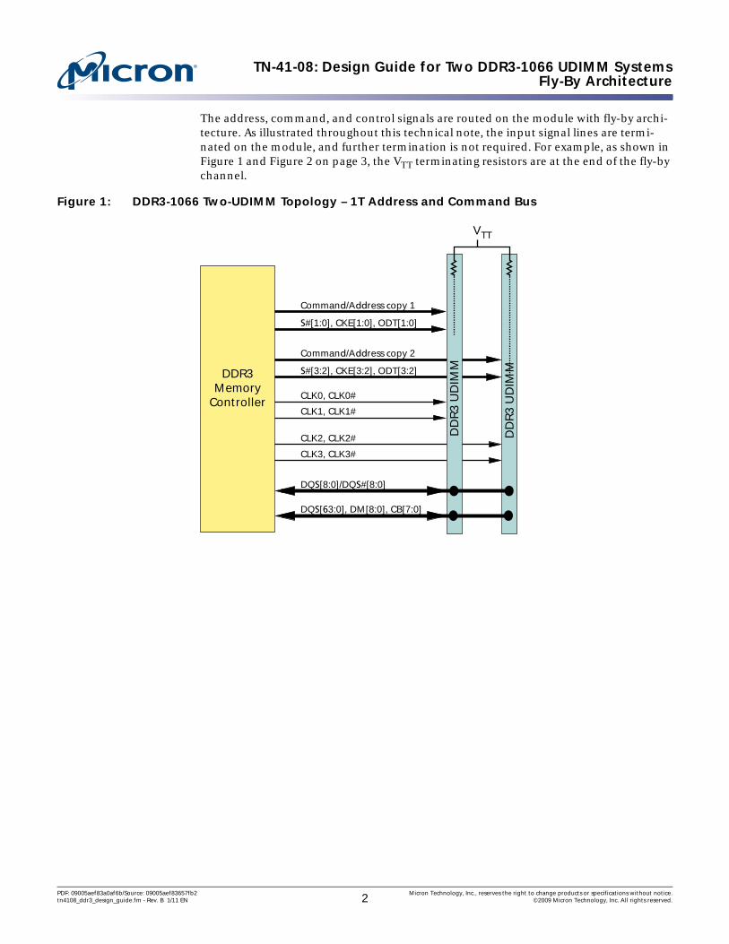
The address, command, and control signals are routed on the module with fly-by archi-tecture. As illustrated throughout this technical note, the input signal lines are termi-nated on the module, and further termination is not required. For example, as shown in Figure 1 and Figure 2 on page 3, the VTT terminating resistors are at the end of the fly-by channel.
Figure 1: DDR3-1066 Two-UDIMM Topology – 1T Address and Command Bus
CLK2, CLK2#
CLK3, CLK3#
VTT
Command/Address copy 1
CLK0, CLK0#
CLK1, CLK1#
DD
R3
UD
IMM
DQS[63:0], DM[8:0], CB[7:0]
DQS[8:0]/DQS#[8:0]
S#[1:0], CKE[1:0], ODT[1:0]
S#[3:2], CKE[3:2], ODT[3:2]
DD
R3
UD
IMM
Command/Address copy 2
DDR3Memory
Controller
PDF: 09005aef83a0af6b/Source: 09005aef83657fb2 Micron Technology, Inc., reserves the right to change products or specifications without notice.tn4108_ddr3_design_guide.fm - Rev. B 1/11 EN 2 ©2009 Micron Technology, Inc. All rights reserved.

TN-41-08: Design Guide for Two DDR3-1066 UDIMM SystemsDDR3 Signal Groups
Figure 2: DDR3-1066 Two-UDIMM Topology – 2T Address and Command Bus
Note that a timing skew exists between the DRAM controller and the various DRAM devices on the DIMM, and the DRAM controller must account for the timing skews. DDR3 modules support write leveling, which is intended to help determine the timing skews. For an in-depth discussion of write-leveling features, refer to Micron’s DDR3 data sheets that discuss write leveling.
DDR3 Signal GroupsThe signals that compose a DDR3 memory bus can be divided into four unique groups, each with its own configuration and routing requirements.• Data group: Data strobe DQS[8:0], data strobe complement DQS#[8:0], data mask
DM[8:0], data DQ[63:0], and check bits CB[7:0] (x72)• Address and command group: Bank addresses BA[2:0]; addresses A[15:0]; and
command inputs, including RAS#, CAS#, and WE#• Control group: Chip select S#[3:0], clock enable CKE[3:0], on-die termination
ODT[3:0], and RESET#0• Clock group: Differential clocks CK[3:0] and CK#[3:0]
Board StackupA two-DIMM DDR3 channel can be routed on a four-layer board. The layout should use controlled impedance traces of ZO = 40Ω (±10%) characteristic impedance. An example board stackup is shown in Figure 3 on page 4. The trace impedance is based on a 5-mil-wide trace and 0.5oz copper (Cu) with a dielectric constant of 4.2 for the FR4 prepreg material. For this stackup, it is assumed that the 0.5oz Cu on the outer layers is plated for a total thickness of 2.1 mils. Other solutions exist to achieve a 40Ω characteristic imped-ance, so board designers should work with their PCB vendors to specify a stackup.
CLK2, CLK2#
CLK3, CLK3#
VTT
Command/Address copy 1
CLK0, CLK0#
CLK1, CLK1#
DD
R3
UD
IMM
DQS[63:0], DM[8:0], CB[7:0]
DQS[8:0]/DQS#[8:0]
S#[1:0], CKE[1:0], ODT[1:0]
S#[3:2], CKE[3:2], ODT[3:2]
DD
R3
UD
IMM
DDR3Memory
Controller
PDF: 09005aef83a0af6b/Source: 09005aef83657fb2 Micron Technology, Inc., reserves the right to change products or specifications without notice.tn4108_ddr3_design_guide.fm - Rev. B 1/11 EN 3 ©2009 Micron Technology, Inc. All rights reserved.

TN-41-08: Design Guide for Two DDR3-1066 UDIMM SystemsDDR3 Command and Address Voltage Margin and Slew Rate
Figure 3: Sample Board Stackup
DDR3 Command and Address Voltage Margin and Slew RateThe primary difference between DDR2 and DDR3 module command, address, and control signals is fly-by topology with impedance matching. Impedance matching is required for proper fly-by operation.
With a single DIMM placed at the end of the motherboard bus, the system is matched throughout. The driver impedance could be as much as 40Ω, but is generally set a little lower; the motherboard is routed at 40Ω; and the DIMM lead-in, which is about 4 inches, is routed at 40Ω. DRAM-to-DRAM routing is 60Ω, but when the additional capacitance of the DRAM devices is taken into account, this lead-in becomes an effective 40Ω impedance. The termination resistor to VTT is 39Ω. This configuration provides fast slew rates and clean edge transitions due to the minimal number of reflections.
For configurations with 2 DIMMs on a channel, a mismatch occurs at the first DIMM. This mismatch will look like 20Ω impedance and there will be a reflection toward the driver. If the driver impedance is 40Ω, the reflection will terminate at the controller. When the signal sees the 20Ω impedance, the amplitude drops by about 50%. After the first DIMM, the impedances are matched, and there will be little reflection from the termination.
Thus the primary effect of using a second DIMM is mostly amplitude reduction. There will also be a slight timing shift and some slew rate change. The slew rate change is due to the amplitude change, not a rise-time change. Rise time is based on a percentage of the total swing, whereas slew rate is based on the amplitude change.
The following figures provide examples of the slew rate change for a two-DIMM device versus a one-DIMM device. The slew rate changes are primarily associated with the amplitude change due to voltage division rather than the capacitive loading that domi-
3.5 mil prepreg
~42 mil core
Ground plane (0.5oz Cu plus plating)
Power plane (0.5oz Cu plus plating)
3.5 mil prepreg
Solder side – signal layer 2(0.5oz Cu)
Component side – signal layer 1(0.5oz Cu)
PDF: 09005aef83a0af6b/Source: 09005aef83657fb2 Micron Technology, Inc., reserves the right to change products or specifications without notice.tn4108_ddr3_design_guide.fm - Rev. B 1/11 EN 4 ©2009 Micron Technology, Inc. All rights reserved.
TN-41-08: Design Guide for Two DDR3-1066 UDIMM SystemsAddress and Command Signals for 2T Clocking
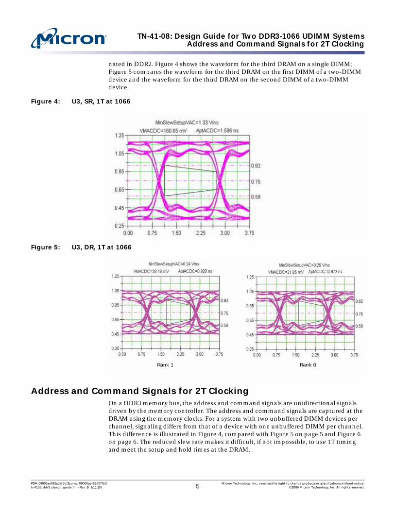
nated in DDR2. Figure 4 shows the waveform for the third DRAM on a single DIMM; Figure 5 compares the waveform for the third DRAM on the first DIMM of a two-DIMM device and the waveform for the third DRAM on the second DIMM of a two-DIMM device.
Figure 4: U3, SR, 1T at 1066
Figure 5: U3, DR, 1T at 1066
Address and Command Signals for 2T ClockingOn a DDR3 memory bus, the address and command signals are unidirectional signals driven by the memory controller. The address and command signals are captured at the DRAM using the memory clocks. For a system with two unbuffered DIMM devices per channel, signaling differs from that of a device with one unbuffered DIMM per channel. This difference is illustrated in Figure 4, compared with Figure 5 on page 5 and Figure 6 on page 6. The reduced slew rate makes it difficult, if not impossible, to use 1T timing and meet the setup and hold times at the DRAM.
Rank 1 Rank 0
PDF: 09005aef83a0af6b/Source: 09005aef83657fb2 Micron Technology, Inc., reserves the right to change products or specifications without notice.tn4108_ddr3_design_guide.fm - Rev. B 1/11 EN 5 ©2009 Micron Technology, Inc. All rights reserved.
TN-41-08: Design Guide for Two DDR3-1066 UDIMM SystemsAddress and Command Signals for 2T Clocking
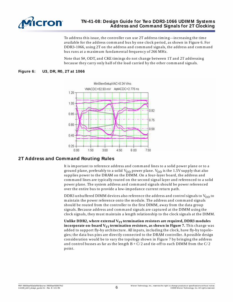
To address this issue, the controller can use 2T address timing—increasing the time available for the address command bus by one clock period, as shown in Figure 6. For DDR3-1066, using 2T on the address and command signals, the address and command bus runs at a maximum fundamental frequency of 266 MHz.
Note that S#, ODT, and CKE timings do not change between 1T and 2T addressing because they carry only half of the load carried by the other command signals.
Figure 6: U3, DR, R0, 2T at 1066
2T Address and Command Routing Rules
It is important to reference address and command lines to a solid power plane or to a ground plane, preferably to a solid VDD power plane. VDD is the 1.5V supply that also supplies power to the DRAM on the DIMM. On a four-layer board, the address and command lines are typically routed on the second signal layer and referenced to a solid power plane. The system address and command signals should be power referenced over the entire bus to provide a low-impedance current return path.
DDR3 unbuffered DIMM devices also reference the address and control signals to VDD to maintain the power reference onto the module. The address and command signals should be routed from the controller to the first DIMM, away from the data group signals. Because address and command signals are captured at the DIMM using the clock signals, they must maintain a length relationship to the clock signals at the DIMM.
Unlike DDR2, where external VTT termination resistors are required, DDR3 modules incorporate on-board VTT termination resistors, as shown in Figure 7. This change was added to support fly-by architecture. All inputs, including the clock, have fly-by topolo-gies; the data bus pins are directly connected to the DRAM controller. A possible design consideration would be to vary the topology shown in Figure 7 by bringing the address and control busses as far as the length B + C/2 and tie-off to each DIMM from the C/2 point.
PDF: 09005aef83a0af6b/Source: 09005aef83657fb2 Micron Technology, Inc., reserves the right to change products or specifications without notice.tn4108_ddr3_design_guide.fm - Rev. B 1/11 EN 6 ©2009 Micron Technology, Inc. All rights reserved.

TN-41-08: Design Guide for Two DDR3-1066 UDIMM SystemsAddress and Command Signals for 2T Clocking
Figure 7: DDR3 Address and Command Signal Group 2T Routing Topology
Notes: 1. This value is controller-dependent.
Parallel/Pull-Up Resistor (VTTR) Termination Resistor
The VTT supply is still required on the motherboard. However, the external parallel termination resistors required for DDR2 are not required for DDR3 JEDEC-compliant modules; the VTT terminating resistors are built onto the module.
Table 1: Address and Command Group 2T Routing Rules
Length
A = Obtain from DRAM controller vendor (“A” is the length from the die pad to the ball on the ASIC package)B = 1.9 to 4.5 inchesC = 0.425 inchesTotal: A + B + C = 2.5 to 5.0 inches
Length Matching
±20 mils of memory clock length at the DIMM1
Trace
Trace width = 5 mils: target 40Ω impedanceTrace space = 12 to 15 mils, reducing to 11.5 mils between the pins of the DIMMTrace space from DIMM pins = 7 milsTrace space to other signal groups = 20 to 25 mils
VTT
DDR3Memory
Controller
Address andcontrol
DIMM 1 DIMM 2
A B
Pad on die Pin on package
C
PDF: 09005aef83a0af6b/Source: 09005aef83657fb2 Micron Technology, Inc., reserves the right to change products or specifications without notice.tn4108_ddr3_design_guide.fm - Rev. B 1/11 EN 7 ©2009 Micron Technology, Inc. All rights reserved.
TN-41-08: Design Guide for Two DDR3-1066 UDIMM SystemsAddress and Command Signals for 1T Clocking
Address and Command Signals for 1T ClockingOn a DDR3 memory bus, the address and command signals are unidirectional signals driven by the memory controller. The address and command signals are captured at the DRAM using the memory clocks. For a system with two unbuffered DIMM devices per channel, the signaling differs from a device with one unbuffered DIMM per channel (see Figure 4 through Figure 6 starting on page 5). The reduced slew rate makes it difficult, if not impossible, to use 1T timing and meet the setup and hold times at the DRAM.
To address this issue, the controller can use 2T address timing—increasing the time available for the address command bus by one clock period, as shown in Figure 6.
To increase the timing margin, loading on the address and command bus must be reduced. Some controllers provide two copies of the address and command bus. One copy is connected to each DIMM, effectively reducing the total maximum load on the bus to one DIMM. With reduced loading, the timing and voltage margin is increased to a point that 1T address bus timing is generally achievable (see Figure 4 on page 5).
Address and command 1T signal-group routing topology is shown in the block diagram in Figure 8 on page 9. For DDR3-1066 using 1T on the address and command signals, the address and command bus runs at a maximum fundamental frequency of 533 MHz.
Adding an extra copy of address and command signals helps improve signaling, but load reduction alone may not be enough to comply with setup and hold times for 1T signals.
1T Address and Command Routing Rules
It is important to reference address and command lines to a solid power plane or to a ground plane.
On a four-layer board, the address and command lines are typically routed on the second signal layer and referenced to a solid power plane. The system address and command signals should be power referenced over the entire bus to provide a low- impedance current return path.
The address and command signals should be routed away from the data group signals, from the controller to the first DIMM. Because address and command signals are captured at the DIMM using the clock signals, they must maintain the length relation-ship to the clock signals at the DIMM.
PDF: 09005aef83a0af6b/Source: 09005aef83657fb2 Micron Technology, Inc., reserves the right to change products or specifications without notice.tn4108_ddr3_design_guide.fm - Rev. B 1/11 EN 8 ©2009 Micron Technology, Inc. All rights reserved.

TN-41-08: Design Guide for Two DDR3-1066 UDIMM SystemsAddress and Command Signals for 1T Clocking
Figure 8: DDR3 Address and Command Signal Group 1T Routing Topology
Notes: 1. This value is controller-dependent.
Setup and Hold Derating
Setup and hold times require derating whenever the slew rate is faster than 1 V/ns. The derating factors can be obtained from the device data sheet. Slew rates slower than 1 V/ns generally do not require derating; however, derating can reclaim some time margin.
Table 2: Address and Command Group 1T Routing Rules
Length
A = Obtain from DRAM controller vendor (“A” is the length from the die pad to the ball on the ASIC package)B = 1.9 to 4.5 inchesC = 0.425 inchesTotal: A + B + C = 2.5 to 5.0 inches
Length Matching
±20 mils of memory clock length at the DIMM1
Trace
Trace width = 5 mils: target 40Ω impedanceTrace space = 12 to 15 mils, reducing to 11.5 mils between the pins of the DIMMTrace space from DIMM pins = 7 milsTrace space to other signal groups = 20 to 25 mils
VTT
DDR3Memory
Controller
Address andcontrol copy 2
DIMM 1 DIMM 2
A B
Pad on die Pin on package
Address andcontrol copy 1
A B
C
PDF: 09005aef83a0af6b/Source: 09005aef83657fb2 Micron Technology, Inc., reserves the right to change products or specifications without notice.tn4108_ddr3_design_guide.fm - Rev. B 1/11 EN 9 ©2009 Micron Technology, Inc. All rights reserved.
TN-41-08: Design Guide for Two DDR3-1066 UDIMM SystemsControl Signals
Additionally, when developing a timing budget, derating the setup and hold times to VREF points is necessary to ensure that all components are using the same timing refer-ence points.
Parallel/Pull-Up Resistor (VTTR) Termination Resistor
The external parallel termination resistors that were required for DDR2 are not required for DDR3 JEDEC-compliant modules; the VTT terminating resistors are built onto the module.
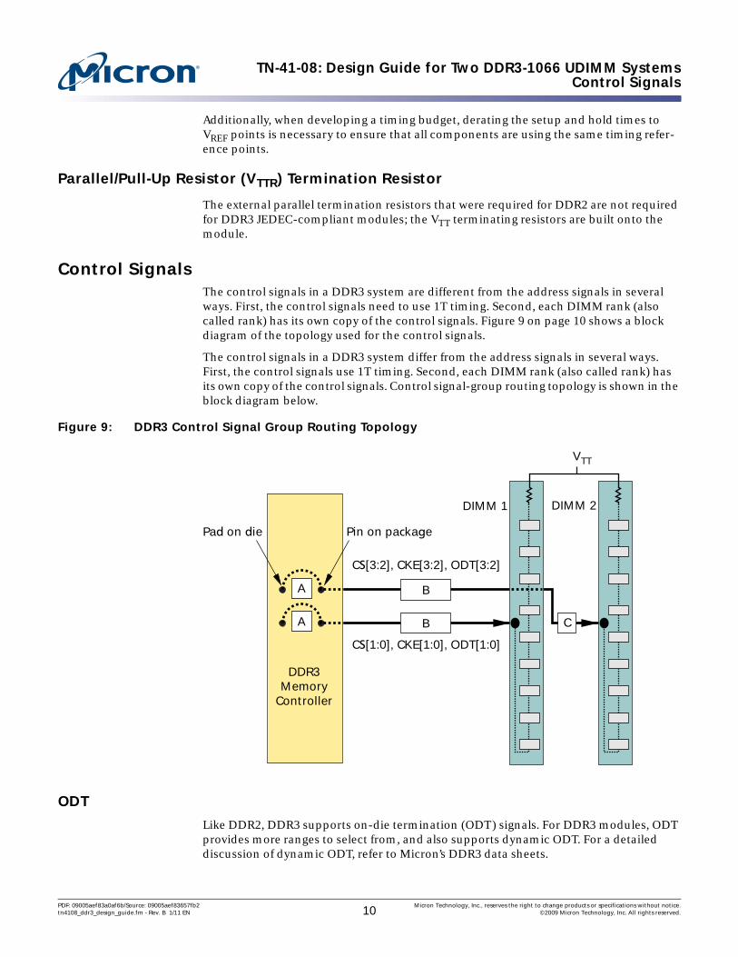
Control SignalsThe control signals in a DDR3 system are different from the address signals in several ways. First, the control signals need to use 1T timing. Second, each DIMM rank (also called rank) has its own copy of the control signals. Figure 9 on page 10 shows a block diagram of the topology used for the control signals.
The control signals in a DDR3 system differ from the address signals in several ways. First, the control signals use 1T timing. Second, each DIMM rank (also called rank) has its own copy of the control signals. Control signal-group routing topology is shown in the block diagram below.
Figure 9: DDR3 Control Signal Group Routing Topology
ODT
Like DDR2, DDR3 supports on-die termination (ODT) signals. For DDR3 modules, ODT provides more ranges to select from, and also supports dynamic ODT. For a detailed discussion of dynamic ODT, refer to Micron’s DDR3 data sheets.
VTT
DDR3Memory
Controller
CS[1:0], CKE[1:0], ODT[1:0]
DIMM 1 DIMM 2
B C
CS[3:2], CKE[3:2], ODT[3:2]
B
Pad on die Pin on package
A
A
PDF: 09005aef83a0af6b/Source: 09005aef83657fb2 Micron Technology, Inc., reserves the right to change products or specifications without notice.tn4108_ddr3_design_guide.fm - Rev. B 1/11 EN 10 ©2009 Micron Technology, Inc. All rights reserved.
TN-41-08: Design Guide for Two DDR3-1066 UDIMM SystemsControl Signals
In DDR3 devices, ODT signals are used to control the termination of the data group signals. DDR3 does not need the external serial and parallel termination resistors on the data group signals used in earlier DDR systems. The enhanced DDR3 ODT termination scheme terminates signals via internal termination resistors in the DRAM device and in the controller. ODT signals are used to turn termination on or off in the DRAM (ODT is enabled or disabled using the mode registers), depending on the type of bus transition and the system load.
ODT Simulations
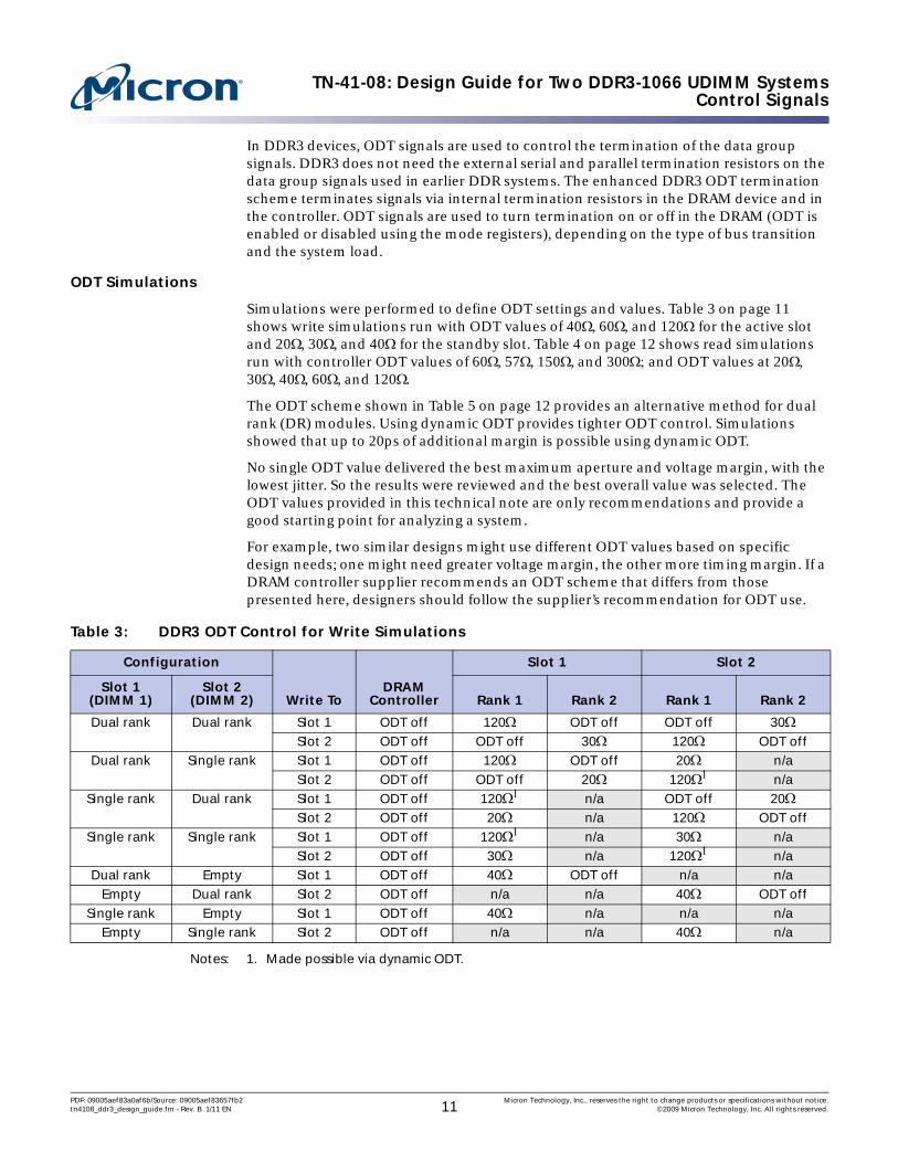
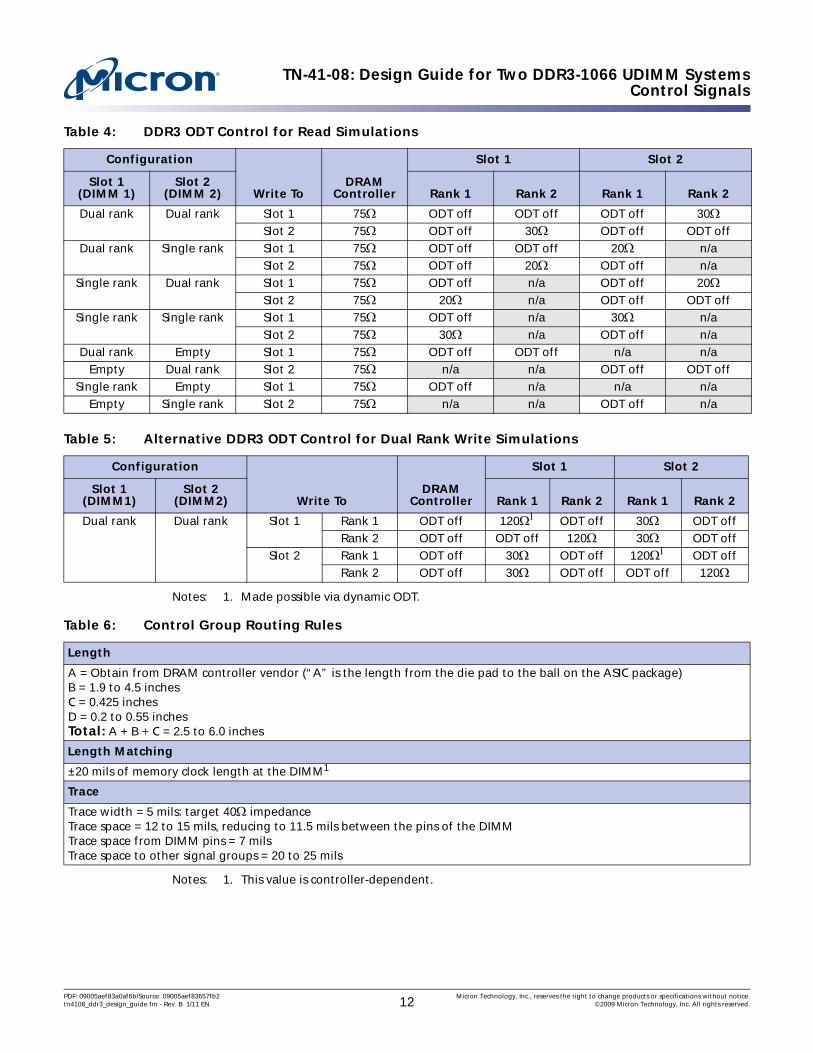
Simulations were performed to define ODT settings and values. Table 3 on page 11 shows write simulations run with ODT values of 40Ω, 60Ω, and 120Ω for the active slot and 20Ω, 30Ω, and 40Ω for the standby slot. Table 4 on page 12 shows read simulations run with controller ODT values of 60Ω, 57Ω, 150Ω, and 300Ω; and ODT values at 20Ω, 30Ω, 40Ω, 60Ω, and 120Ω.
The ODT scheme shown in Table 5 on page 12 provides an alternative method for dual rank (DR) modules. Using dynamic ODT provides tighter ODT control. Simulations showed that up to 20ps of additional margin is possible using dynamic ODT.
No single ODT value delivered the best maximum aperture and voltage margin, with the lowest jitter. So the results were reviewed and the best overall value was selected. The ODT values provided in this technical note are only recommendations and provide a good starting point for analyzing a system.
For example, two similar designs might use different ODT values based on specific design needs; one might need greater voltage margin, the other more timing margin. If a DRAM controller supplier recommends an ODT scheme that differs from those presented here, designers should follow the supplier’s recommendation for ODT use.
Notes: 1. Made possible via dynamic ODT.
Table 3: DDR3 ODT Control for Write Simulations
Configuration
Write ToDRAM
Controller
Slot 1 Slot 2
Slot 1(DIMM 1)
Slot 2(DIMM 2) Rank 1 Rank 2 Rank 1 Rank 2
Dual rank Dual rank Slot 1 ODT off 120Ω ODT off ODT off 30ΩSlot 2 ODT off ODT off 30Ω 120Ω ODT off
Dual rank Single rank Slot 1 ODT off 120Ω ODT off 20Ω n/aSlot 2 ODT off ODT off 20Ω 120Ω1 n/a
Single rank Dual rank Slot 1 ODT off 120Ω1 n/a ODT off 20ΩSlot 2 ODT off 20Ω n/a 120Ω ODT off
Single rank Single rank Slot 1 ODT off 120Ω1 n/a 30Ω n/aSlot 2 ODT off 30Ω n/a 120Ω1 n/a
Dual rank Empty Slot 1 ODT off 40Ω ODT off n/a n/aEmpty Dual rank Slot 2 ODT off n/a n/a 40Ω ODT off
Single rank Empty Slot 1 ODT off 40Ω n/a n/a n/aEmpty Single rank Slot 2 ODT off n/a n/a 40Ω n/a
PDF: 09005aef83a0af6b/Source: 09005aef83657fb2 Micron Technology, Inc., reserves the right to change products or specifications without notice.tn4108_ddr3_design_guide.fm - Rev. B 1/11 EN 11 ©2009 Micron Technology, Inc. All rights reserved.
TN-41-08: Design Guide for Two DDR3-1066 UDIMM SystemsControl Signals
Notes: 1. Made possible via dynamic ODT.
Notes: 1. This value is controller-dependent.
Table 4: DDR3 ODT Control for Read Simulations
Configuration
Write ToDRAM
Controller
Slot 1 Slot 2
Slot 1(DIMM 1)
Slot 2(DIMM 2) Rank 1 Rank 2 Rank 1 Rank 2
Dual rank Dual rank Slot 1 75Ω ODT off ODT off ODT off 30ΩSlot 2 75Ω ODT off 30Ω ODT off ODT off
Dual rank Single rank Slot 1 75Ω ODT off ODT off 20Ω n/aSlot 2 75Ω ODT off 20Ω ODT off n/a
Single rank Dual rank Slot 1 75Ω ODT off n/a ODT off 20ΩSlot 2 75Ω 20Ω n/a ODT off ODT off
Single rank Single rank Slot 1 75Ω ODT off n/a 30Ω n/aSlot 2 75Ω 30Ω n/a ODT off n/a
Dual rank Empty Slot 1 75Ω ODT off ODT off n/a n/aEmpty Dual rank Slot 2 75Ω n/a n/a ODT off ODT off
Single rank Empty Slot 1 75Ω ODT off n/a n/a n/aEmpty Single rank Slot 2 75Ω n/a n/a ODT off n/a
Table 5: Alternative DDR3 ODT Control for Dual Rank Write Simulations
Configuration
Write ToDRAM
Controller
Slot 1 Slot 2
Slot 1(DIMM1)
Slot 2(DIMM2) Rank 1 Rank 2 Rank 1 Rank 2
Dual rank Dual rank Slot 1 Rank 1 ODT off 120Ω1 ODT off 30Ω ODT offRank 2 ODT off ODT off 120Ω 30Ω ODT off
Slot 2 Rank 1 ODT off 30Ω ODT off 120Ω1 ODT offRank 2 ODT off 30Ω ODT off ODT off 120Ω
Table 6: Control Group Routing Rules
Length
A = Obtain from DRAM controller vendor (“A” is the length from the die pad to the ball on the ASIC package)B = 1.9 to 4.5 inchesC = 0.425 inchesD = 0.2 to 0.55 inchesTotal: A + B + C = 2.5 to 6.0 inches
Length Matching
±20 mils of memory clock length at the DIMM1
Trace
Trace width = 5 mils: target 40Ω impedanceTrace space = 12 to 15 mils, reducing to 11.5 mils between the pins of the DIMMTrace space from DIMM pins = 7 milsTrace space to other signal groups = 20 to 25 mils
PDF: 09005aef83a0af6b/Source: 09005aef83657fb2 Micron Technology, Inc., reserves the right to change products or specifications without notice.tn4108_ddr3_design_guide.fm - Rev. B 1/11 EN 12 ©2009 Micron Technology, Inc. All rights reserved.

TN-41-08: Design Guide for Two DDR3-1066 UDIMM SystemsData Signals
Control Signal Routing Rules
Similar to the address signals, the control signals must be referenced to a solid power plane or to a ground plane. On a four-layer board, the control signals are typically routed on the bottom signal layer and referenced to a solid power plane. The system control signals must be power referenced over the entire bus to provide a Low-Z current return path. Unlike address signals, control signals are routed point-to-point from the controller to the DIMM.
The control signals do not require any series or parallel resistance. The control signals must be routed with clearance from the data group signals, from the controller to the first DIMM. Because the control signals are captured at the DIMM using the clock signals, they must maintain the length relationship to the clock signals at the DIMM.
Parallel/Pull-up Resistor (VTTR) Termination Resistor
The external parallel termination resistors that were required for DDR2 are no longer required with DDR3 JEDEC-compliant modules because the VTT terminating resistors are built onto the module.
Data SignalsIn a DDR3 system, the data is captured by the memory and the controller using the data strobe (DQS and DQS#) rather than the clock. The data strobe complement (DQS#) must be routed as a differential pair with the data strobe (DQS). To achieve the double data rate, data is captured on each crossing point of the DQS/DQS# pairs. Each eight bits of data has an associated data strobe (DQS and DQS#) and data mask (DM) bit. Because the data is captured off the strobe, the data bits associated with the strobe must be length-matched closely to their strobe bit. This grouping of data and data strobe is referred to as a byte lane. The length matching among byte lanes is not as tight as it is within the byte lane. Figure 10 shows the signals in a single-byte lane and the bus topology for the data signals; Table 7 shows the data and data strobe byte-lane groups.
PDF: 09005aef83a0af6b/Source: 09005aef83657fb2 Micron Technology, Inc., reserves the right to change products or specifications without notice.tn4108_ddr3_design_guide.fm - Rev. B 1/11 EN 13 ©2009 Micron Technology, Inc. All rights reserved.

TN-41-08: Design Guide for Two DDR3-1066 UDIMM SystemsData Signals
Figure 10: DDR3 Data Byte Lane Routing and Bus Topology
Data Signal Routing Rules
It is important that the data lines be referenced to a solid ground plane. These high-speed data signals require a good ground return path to avoid signal quality degradation due to inductance in the signal return path. The system data signals should be ground-referenced from the memory controller to the DIMM connectors, and from DIMM connector to DIMM connector to provide a Low-Z current return path. This is accom-plished by routing the data signals on the top layer for the entire length of the signal. The data signals should not have any vias. If this cannot be avoided, then the time delay associated with the via should be accounted for in the trace length.
Table 7: Data and Data Strobe Byte Lane Groups
Data Data Strobe Data Strobe Complement Data Mask
DQ[7:0] DQS0 DQS#0 DM0
DQ[15:8] DQS1 DQS#1 DM1
DQ[23:16] DQS2 DQS#2 DM2
DQ[31:24] DQS3 DQS#3 DM3
DQ[39:32] DQS4 DQS#4 DM4
DQ[47:40] DQS5 DQS#5 DM5
DQ[55:48] DQS6 DQS#6 DM6
DQ[63:56] DQS7 DQS#7 DM7
CB[7:0] DQS8 DQS#8 DM8
DDR3Memory
Controller
DM [X]
DIMM 1 DIMM 2
B C
DQS, DQS# [X]
B C
DQ byte group [X]
B
Pad on die Pin on package
C
A
A
A
PDF: 09005aef83a0af6b/Source: 09005aef83657fb2 Micron Technology, Inc., reserves the right to change products or specifications without notice.tn4108_ddr3_design_guide.fm - Rev. B 1/11 EN 14 ©2009 Micron Technology, Inc. All rights reserved.

TN-41-08: Design Guide for Two DDR3-1066 UDIMM SystemsClock Signals
Notes: 1. Differential signals have a faster propagation time than single-ended signals. If the data signals are routed slightly shorter than the data strobe, the data strobe signal will arrive at the DRAM in the center of its associated data signals. Because the propagation delay can vary with design parameters, simulating these signals is recommended.
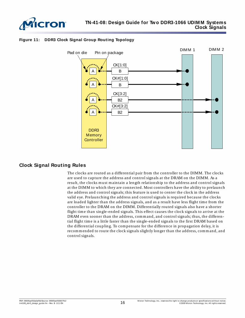
Clock SignalsThe memory clocks CK[4:0] and CK#[4:0] are used by the DRAM on a DDR3 bus to capture the address and command data. Unbuffered DIMM devices require two clock pairs per DIMM. Some DDR3 memory controllers drive all these clocks, and others require an external clock driver to generate these signals. This technical note assumes that the memory controller will drive the four clock pairs required for a two-DIMM unbuffered system. Clocks are not terminated to VTT like the address signals of a DDR3 bus. The clocks are differential and must be routed as a differential pair. Each clock pair is differentially terminated on the DIMM. Figure 11 on page 16 illustrates the routing topology used for the clocks, but in this example, only one of the two clock pairs required per DIMM is shown.
Table 8: Data Group Routing Rules
Length
A = Obtain from DRAM controller vendor (“A” is the length from the die pad to the ball on the ASIC package)B = 1.9 to 4.5 inchesC = 0.425 inchesTotal: A + B + C = 2.5 to 5.0 inches
Length Matching in Data/Strobe Byte Lane
±20 mils data strobe, data strobe complement1
100 mils for each byte lane
Length Matching in Byte Lane to Byte Lane
Not required; de-skewing is required because of fly-by topology on the address command bus
Trace
DataTrace width = 7.9 mils: target 40Ω impedanceTrace space = 11.8 mils minimumTrace space from DIMM pins = 7 milsTrace space to other signal groups = 12 milsDifferential StrobeTrace width = 7.9 mils: target 40Ω impedanceTrace space = 4 mils between pairsTrace space to other signals = 15.8 mils
PDF: 09005aef83a0af6b/Source: 09005aef83657fb2 Micron Technology, Inc., reserves the right to change products or specifications without notice.tn4108_ddr3_design_guide.fm - Rev. B 1/11 EN 15 ©2009 Micron Technology, Inc. All rights reserved.
TN-41-08: Design Guide for Two DDR3-1066 UDIMM SystemsClock Signals
Figure 11: DDR3 Clock Signal Group Routing Topology
Clock Signal Routing Rules
The clocks are routed as a differential pair from the controller to the DIMM. The clocks are used to capture the address and control signals at the DRAM on the DIMM. As a result, the clocks must maintain a length relationship to the address and control signals at the DIMM to which they are connected. Most controllers have the ability to prelaunch the address and control signals; this feature is used to center the clock in the address valid eye. Prelaunching the address and control signals is required because the clocks are loaded lighter than the address signals, and as a result have less flight time from the controller to the DRAM on the DIMM. Differentially routed signals also have a shorter flight time than single-ended signals. This effect causes the clock signals to arrive at the DRAM even sooner than the address, command, and control signals; thus, the differen-tial flight time is a little faster than the single-ended signals to the first DRAM based on the differential coupling. To compensate for the difference in propagation delay, it is recommended to route the clock signals slightly longer than the address, command, and control signals.
CK[1:0]
CK#[1:0]
CK[3:2]
CK#[3:2]
Pad on die Pin on packageDIMM 1 DIMM 2
A B
A
A
B
B2
DDR3Memory
Controller
A B2
PDF: 09005aef83a0af6b/Source: 09005aef83657fb2 Micron Technology, Inc., reserves the right to change products or specifications without notice.tn4108_ddr3_design_guide.fm - Rev. B 1/11 EN 16 ©2009 Micron Technology, Inc. All rights reserved.
TN-41-08: Design Guide for Two DDR3-1066 UDIMM SystemsDDR3 Memory Power Supply Requirements
DDR3 Memory Power Supply RequirementsA DDR3 bus implementation requires three separate power supplies. The DRAM and the memory portion of the controller require a 1.5V supply. The 1.5V supply provides power for the DRAM core and I/O, and at a minimum, the I/O of the DRAM controller. The second power supply is VREF, which is used as a reference voltage by the DRAM and the controller. The third power supply is VTT, the bus termination supply. Table 10 on page 18 summarizes the tolerances for each of these supplies.
VREF Voltage and Layout Recommendations
DDR3 supports a separate VREF for address, command, and control pins (VREFCA) and for the data bus (VREFDQ). VREFCA and VREFDQ may come from the same power source, but they should be routed to and then decoupled separately at the DDR3 DIMM. Note that the term VREF applies to both VREFCA and VREFDQ.
The memory reference voltage, VREF, requires a voltage level of half VDD/VDDQ with the tolerance shown in Table 10. VREF can be generated using a simple resistor divider with 1% or better accuracy. VREF must track half VDD/VDDQ over voltage, noise, and tempera-ture changes. Peak-to-peak AC noise on VREF must not exceed ±2% VREF(DC). To ensure a solid DDR3 design, it is imperative that the VREF noise, including crosstalk, is kept to a minimum.
When implementing VREF, consider the following layout recommendations:• Use a 30 mil trace between the decoupling cap and the destination.• Maintain a 15 mil clearance from other nets.• Simplify implementation by routing VREF on the top signal trace layer.• Isolate VREF and/or shield with ground.• Decouple using distributed 0.01µf and 0.1µf capacitors by the regulator, controller,
and DIMM slots. Place one 0.01µf and one 0.1µf near the VREF pin of each DIMM. Place one 0.1µf near the source of VREF, one near the VREF pin on the controller, and two between the controller and the first DIMM.
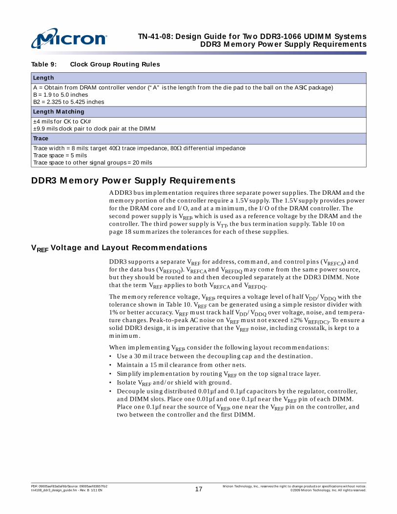
Table 9: Clock Group Routing Rules
Length
A = Obtain from DRAM controller vendor (“A” is the length from the die pad to the ball on the ASIC package)B = 1.9 to 5.0 inchesB2 = 2.325 to 5.425 inches
Length Matching
±4 mils for CK to CK#±9.9 mils clock pair to clock pair at the DIMM
Trace
Trace width = 8 mils: target 40Ω trace impedance, 80Ω differential impedanceTrace space = 5 milsTrace space to other signal groups = 20 mils
PDF: 09005aef83a0af6b/Source: 09005aef83657fb2 Micron Technology, Inc., reserves the right to change products or specifications without notice.tn4108_ddr3_design_guide.fm - Rev. B 1/11 EN 17 ©2009 Micron Technology, Inc. All rights reserved.

TN-41-08: Design Guide for Two DDR3-1066 UDIMM SystemsBoard Layout Design Guidelines
VTT Voltage and Layout Recommendations
The memory termination voltage (VTT), requires current at a voltage level of 750 mV(DC). VTT must be generated by a regulator that is able to sink and source reason-able amounts of current while still maintaining tight voltage regulation. Like VREF imple-mentation, it is also imperative that when implementing VTT, the VTT voltage is kept as stable as possible and that all noise, including crosstalk, is kept to a minimum. VTT must also track variations in VDD/VDDQ over voltage, temperature, and noise ranges, and VTT of the transmitting device must track VREF of the receiving device.
When implementing VTT, consider the following layout recommendations:• Place the VTT island on the component-side signal layer near the VTT pins of the
DIMM socket.• Place the VTT generator as close as possible to the island to minimize impedance
(inductance).• Place two or four 0.1µf decoupling capacitors at the VTT lead to the DIMM on the VTT
island; this minimizes the noise on VTT. Place other bulk decoupling (10–22µf) on the VTT island.
Board Layout Design GuidelinesTo help ensure good signaling, consider the following board design guidelines:• Avoid crossing splits in the power plane• Separate supplies and/or flip-chip packaging to help avoid having SSO on the
controller, which collapses strobes/clocks• Add low-pass VREF filtering on the controller to improve noise margin• Minimize VREF noise:
– Separate supplies or use flip-chip packaging– Use spacing techniques similar to those recommended for signals implementing
VREF– Use the widest trace practical between decoupling capacitors and DIMM VTT pins– Maintain a single reference (either ground or VDD) between the decoupling capaci-
tor and the DRAM VREF pin• Minimize ISI by keeping impedances matched• Minimize crosstalk by isolating sensitive bits, such as strobes, and avoiding return-
path discontinuities
Table 10: Tolerances of the Required Power Supply Voltages
Parameter Symbol Min Typical Max Unit
Device supply voltage VDD 1.425 1.5 1.575 V
Memory reference voltage VREF VDD × 0.49 VDD × 0.5 VDD × 0.51 V
Memory termination voltage VTT VREF - 40mV VREF VREF + 40mV V
PDF: 09005aef83a0af6b/Source: 09005aef83657fb2 Micron Technology, Inc., reserves the right to change products or specifications without notice.tn4108_ddr3_design_guide.fm - Rev. B 1/11 EN 18 ©2009 Micron Technology, Inc. All rights reserved.

TN-41-08: Design Guide for Two DDR3-1066 UDIMM SystemsDDR3 Timing Budgets
DDR3 Timing BudgetsThe first section of this technical note discussed DDR3 memory bus functions, the general relationship among the signals on the bus, and provided examples. If a design deviates from the examples provided, the routing rules for the design can change.
Because it is unlikely that every design will follow the examples exactly, it is important to simulate the design. One of the objectives of simulation is to determine whether the design will meet the signal timing requirements of the DIMM and DDR3 controller. To meet this objective, a timing budget must be generated. The following sections show how to use the data provided in the DDR3 DIMM and DDR3 controller data sheets to determine the amount of the total timing budget that can be allocated for board inter-connect use.
Calculating DDR3 Data Write Budgets
Timing budgets for DDR3 WRITEs at 1066 MT/s and 800 MT/s are broken out in Table 11 on page 19. The portions of the budget consumed by the DRAM device and by the DDR3 controller are fixed and cannot be influenced by the board designer. The amount of the total budget remaining after subtracting the portion consumed by the DRAM and the controller is what remains for use by the board interconnect. This is the portion used to determine the bus routing rules. The different components of the board interconnect are outlined. The board designer can make trade-offs with trace spacing, length matching, and resistor tolerance to determine the most suitable interconnect solution for a given design.
Table 11: DDR3 Write Budget
Element Skew Component
DDR3-800 DDR3-1066
Unit CommentsSetup Hold Setup Hold
Clock Data/strobe chip PLL jitter 45 45 45 45 ps
DRAM tJITper 50 50 45 45 ps Derate what the DRAM is tested forClock skew 0 0 0 0 ps
Transmitter Controller skew 267 267 209 209 ps Assume similar to DRAM and use DRAM’s specifications
Interconnect DQ crosstalk and ISI1 52 52 32 32 ps 1 victim (1010...), 4 aggressors (PRBS)DQS crosstalk and ISI1 23 23 23 23 ps 1 shielded victim (1010...), 2
aggressors (PRBS)VREF reduction 10 10 10 10 ps ±30mV in DRAM skew, additional
±10 mV/(1 V/ns)REFF mismatch 0 0 0 0 ps ±6% accounted for by DRAM
specificationPath matching (board) 10 10 10 10 ps Within byte lane: 165 ps/in;
mismatch within DQS to DQPath matching (module) 5 5 5 5 ps Module routing skew (30%
reduction with leveling)Input capacitance matching
5 5 5 5 ps Strobe to data variation
ODT skew (1%) 5 5 5 5 ps EstimatedTotal interconnect 110 110 90 90 ps
Receiver DRAM skew 215 215 165 165 ps tDS, tDH from DRAM specification, derated for faster slew rates
PDF: 09005aef83a0af6b/Source: 09005aef83657fb2 Micron Technology, Inc., reserves the right to change products or specifications without notice.tn4108_ddr3_design_guide.fm - Rev. B 1/11 EN 19 ©2009 Micron Technology, Inc. All rights reserved.

TN-41-08: Design Guide for Two DDR3-1066 UDIMM SystemsDDR3 Timing Budgets
Notes: 1. Assumes uncoupled package model. When using a coupled package model, expect an increase of uncertainty from15ps to 30ps.
Calculating DRAM Write Budget Consumption
The amount of the write budget consumed by the DRAM is provided in the DDR3 data sheets. The data sheets also provide the data input hold time (tDH) relative to strobe and the data input setup time (tDS) relative to strobe. These values generally should not be entered directly into the timing budgets for setup and hold. It is important to derate the DRAM setup and hold times to account for any slew rate variations. The setup and hold times should also be converted from the trip-point specifications to VREF-based values. Failure to do so could result in margin calculations that exceed what is actually available.
Calculating DDR3 Controller Write Budget Consumption
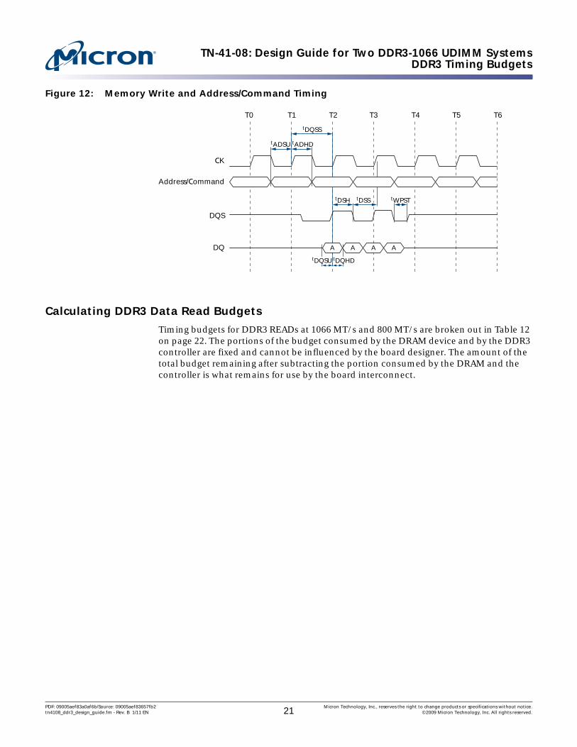
To calculate the amount of the setup timing budget consumed by the DDR3 controller on a DRAM WRITE, find the value for tDQSU MIN. This is the minimum amount of time all data will be valid before the data strobe transitions, as shown in Figure 12. tDQSU should take clock asymmetry into account. In an ideal situation, tDQSU would be equal to 1/4 × tCK. The difference between 1/4 × tCK and tDQSU is the amount of the write timing budget consumed by the controller for setup. From this, the following equation is derived:
Controller setup data valid reduction = 1/4 × tCK - tDQSU (EQ 1)
To calculate the hold time, use the same equation, tDQHD in place of tDQSU.
Total loss Total skew 592 592 464 464 ps Transmitter + receiver + interconnect skews
MAX eye Time available 625 625 469 469 ps Total time availableBudget (4L) Timing margin 33 33 5 5 ps 4-layer (microstrip) 40Ω, 0.135mm
trace to trace4L to 6L DQ crosstalk and ISI 9 9 9 9 ps Reduction using microstrip versus
striplineDQS crosstalk and ISI 19 19 19 19 ps Reduction using microstrip versus
striplineBudget (6L) Timing margin 61 61 33 33 ps 6-layer (stripline) 40Ω, 0.135mm
trace to traceDRAM specifications
tDS 75 75 25 25 ps Specification at 1 V/ns at VIH(AC)tDSVREF 211 211 161 161 ps Specification derated to 1.5 V/ns,
then adjusted to VREFtDH 150 150 100 100 ps Specification at 1 V/ns at VIH(AC)tDHVREF 218 218 168 168 ps Specification derated to 1.9 V/ns,
then adjusted to VREF
Table 11: DDR3 Write Budget (continued)
Element Skew Component
DDR3-800 DDR3-1066
Unit CommentsSetup Hold Setup Hold
PDF: 09005aef83a0af6b/Source: 09005aef83657fb2 Micron Technology, Inc., reserves the right to change products or specifications without notice.tn4108_ddr3_design_guide.fm - Rev. B 1/11 EN 20 ©2009 Micron Technology, Inc. All rights reserved.
TN-41-08: Design Guide for Two DDR3-1066 UDIMM SystemsDDR3 Timing Budgets
Figure 12: Memory Write and Address/Command Timing
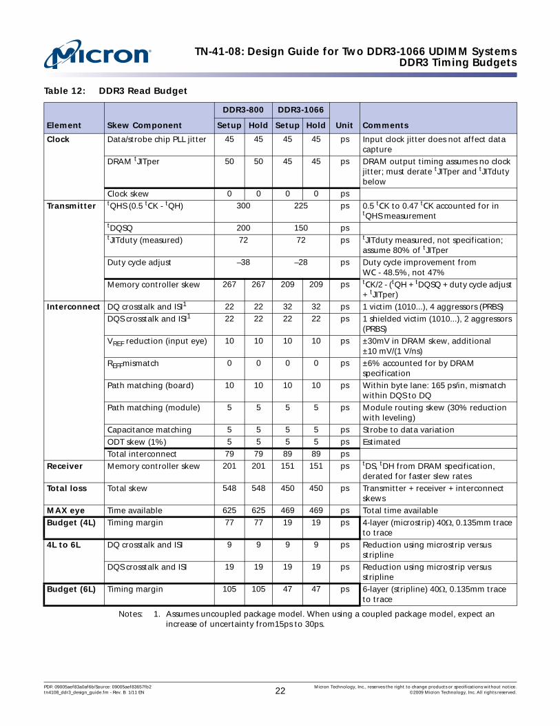
Calculating DDR3 Data Read Budgets
Timing budgets for DDR3 READs at 1066 MT/s and 800 MT/s are broken out in Table 12 on page 22. The portions of the budget consumed by the DRAM device and by the DDR3 controller are fixed and cannot be influenced by the board designer. The amount of the total budget remaining after subtracting the portion consumed by the DRAM and the controller is what remains for use by the board interconnect.
T0 T2 T3 T4 T5 T6
tADSU tADHD
tDSStDSH
tDQSS
T1
DQS
DQ AA A A
tWPST
CK
Address/Command
tDQSU tDQHD
PDF: 09005aef83a0af6b/Source: 09005aef83657fb2 Micron Technology, Inc., reserves the right to change products or specifications without notice.tn4108_ddr3_design_guide.fm - Rev. B 1/11 EN 21 ©2009 Micron Technology, Inc. All rights reserved.
TN-41-08: Design Guide for Two DDR3-1066 UDIMM SystemsDDR3 Timing Budgets
Notes: 1. Assumes uncoupled package model. When using a coupled package model, expect an increase of uncertainty from15ps to 30ps.
Table 12: DDR3 Read Budget
Element Skew Component
DDR3-800 DDR3-1066
Unit CommentsSetup Hold Setup Hold
Clock Data/strobe chip PLL jitter 45 45 45 45 ps Input clock jitter does not affect data capture
DRAM tJITper 50 50 45 45 ps DRAM output timing assumes no clock jitter; must derate tJITper and tJITduty below
Clock skew 0 0 0 0 ps
Transmitter tQHS (0.5 tCK - tQH) 300 225 ps 0.5 tCK to 0.47 tCK accounted for in tQHS measurement
tDQSQ 200 150 pstJITduty (measured) 72 72 ps tJITduty measured, not specification;
assume 80% of tJITperDuty cycle adjust –38 –28 ps Duty cycle improvement from
WC - 48.5%, not 47%Memory controller skew 267 267 209 209 ps tCK/2 - (tQH + tDQSQ + duty cycle adjust
+ tJITper)Interconnect DQ crosstalk and ISI1 22 22 32 32 ps 1 victim (1010...), 4 aggressors (PRBS)
DQS crosstalk and ISI1 22 22 22 22 ps 1 shielded victim (1010...), 2 aggressors (PRBS)
VREF reduction (input eye) 10 10 10 10 ps ±30mV in DRAM skew, additional ±10 mV/(1 V/ns)
REFFmismatch 0 0 0 0 ps ±6% accounted for by DRAM specification
Path matching (board) 10 10 10 10 ps Within byte lane: 165 ps/in, mismatch within DQS to DQ
Path matching (module) 5 5 5 5 ps Module routing skew (30% reduction with leveling)
Capacitance matching 5 5 5 5 ps Strobe to data variationODT skew (1%) 5 5 5 5 ps EstimatedTotal interconnect 79 79 89 89 ps
Receiver Memory controller skew 201 201 151 151 ps tDS, tDH from DRAM specification, derated for faster slew rates
Total loss Total skew 548 548 450 450 ps Transmitter + receiver + interconnect skews
MAX eye Time available 625 625 469 469 ps Total time availableBudget (4L) Timing margin 77 77 19 19 ps 4-layer (microstrip) 40Ω, 0.135mm trace
to trace4L to 6L DQ crosstalk and ISI 9 9 9 9 ps Reduction using microstrip versus
striplineDQS crosstalk and ISI 19 19 19 19 ps Reduction using microstrip versus
striplineBudget (6L) Timing margin 105 105 47 47 ps 6-layer (stripline) 40Ω, 0.135mm trace
to trace
PDF: 09005aef83a0af6b/Source: 09005aef83657fb2 Micron Technology, Inc., reserves the right to change products or specifications without notice.tn4108_ddr3_design_guide.fm - Rev. B 1/11 EN 22 ©2009 Micron Technology, Inc. All rights reserved.

TN-41-08: Design Guide for Two DDR3-1066 UDIMM SystemsDDR3 Timing Budgets
Calculating DRAM Read Budget Consumption
Figure 13 illustrates how the values from the DRAM data sheet affects the total data valid window because the data is driven from the DRAM device. These values are used in the timing budget to determine the portion of the total data timing budget consumed by the DRAM device.
The total budget for the data is half the clock period. This time is halved again to deter-mine the time allowed for setup and hold. Using the DRAM data sheet and filling in numbers for the timing parameters in Figure 13, the total data valid window at the DRAM can be calculated using the following equations:
DVW = tHP - tDQSQ - tQHS (EQ 2)
tCK/2 - DVW/2 = DRAM data valid reduction (EQ 3)
The DRAM data valid reduction is used in the timing budget for setup and hold.
Figure 13: DRAM Read Data Valid
Calculating DDR3 Controller Read Budget Consumption
When read data is received at the controller from the DRAM, the strobe is edge-aligned with the data. The controller must delay the strobe and then use the delayed strobe to capture the read data. Each controller has a minimum value it can accept for a data valid window and a minimum setup and hold time that the data must maintain from the internally delayed strobe. Half the data valid window is the setup or hold time required by the controller, plus any controller-introduced signal skew and strobe-centering uncertainty. The timing diagram in Figure 14 on page 24 provides an example of the timing parameters required for calculating the data valid window. tDQSQ is the maximum delay from the last data signal to go valid after the strobe transitions. tQH is the minimum time all data must remain valid following a strobe transition. Use the following equation to obtain tDV:
tDV = tQH - tDQSQ (EQ 4)
Assuming that tDV is split evenly between setup and hold, the portion of the timing budget consumed by the controller for setup and hold is 1/2 tDV. For the controller used in this example, an even split between setup and hold can be assumed because the controller determining the center of the data eye during the boot-up routine and the DLL maintain this relationship over temperature and voltage variations.
DQS
DQ (last data valid)
DQ (first data no longer valid)
All DQ and DQS, collectively
DVW = 506.25ps
tQH = 656.25ps tQHS = 225ps
tCK/2 = 937.5ps
tHP = 881.25ps (tCK @ 47/53) clock duty cyle = 47/53%
tDQSQ = 150ps
Data valid window
PDF: 09005aef83a0af6b/Source: 09005aef83657fb2 Micron Technology, Inc., reserves the right to change products or specifications without notice.tn4108_ddr3_design_guide.fm - Rev. B 1/11 EN 23 ©2009 Micron Technology, Inc. All rights reserved.

TN-41-08: Design Guide for Two DDR3-1066 UDIMM SystemsDDR3 Timing Budgets
Figure 14: Read Data Timing
CK
DQ (last data valid)
T0 T1 T2 T3 T4
tDQSQ
DQ (first data nolonger valid)
DQ (byte), collectively
DQS
tDVtDVtDVtDV
tQH
D D D DD D D D
D D D DD D D DD D D D
D D D DD D D D
tQH tQH tQH
D D D D
tDQSQ tDQSQ tDQSQ
tHP tHP tHP tHP tHP tHP tHP
PDF: 09005aef83a0af6b/Source: 09005aef83657fb2 Micron Technology, Inc., reserves the right to change products or specifications without notice.tn4108_ddr3_design_guide.fm - Rev. B 1/11 EN 24 ©2009 Micron Technology, Inc. All rights reserved.

TN-41-08: Design Guide for Two DDR3-1066 UDIMM SystemsCalculating 2T Address Timing Budgets
Calculating 2T Address Timing BudgetsTiming budgets for the 2T address and command at a 1066 MHz clock rate are broken out in Table 13. Running the address and command at T2 with a 533 MHz clock results in an address frequency of 266 MHz. The portion of the budget consumed by the DRAM device and the DDR3 controller is fixed and cannot be influenced by the board designer. The amount of the total budget remaining after subtracting the portion consumed by the DRAM and the controller is what remains for use by the board interconnect.
Notes: 1. These are worst-case slow numbers (95°C, 1.7V, slow process).2. The address crosstalk and ISI are approximately 80ps larger because the output driver did
not have uniform pull-up and pull-down transistors; these values are determined at VREF.
Calculating DRAM Address Budget Consumption
To determine the portion of the address budget consumed by the DRAM, use the value of tIS for setup and the value of tIH for hold. These are the setup and hold times required by the DRAM inputs. For systems with heavy loading on the address and command lines, the value in the data sheet must be derated, depending on the slew rate. See the DDR3 data sheet for derating information.
Calculating Controller Address Budget Consumption
The DRAM controller will provide a minimum setup and hold time for the address and command signals with respect to clock. This is the amount of the setup and hold budget consumed by the controller.
Table 13: 2T Address Timing Budget1
Element Skew Component
DDR3-800 DDR3-1066
Unit CommentsSetup Hold Setup Hold
Transmitter Memory controller 300 300 300 300 ps ChipsetReceiver DRAM skew 640 640 560 560 ps tIS, tIH DRAM specification (0.3 V/ns to
1 V/ns)Interconnect Crosstalk: address 162 162 162 162 ps 1 victim (1010...), 4 aggressors (PRBS)
ISI: address 165 165 165 165 ps (PRBS)Crosstalk: clock 25 25 25 25 ps
VREF: reduction 35 35 35 35 ps ±30mV included in DRAM skew; additional = (±20mV)/(0.3 V/ns)
Path matching 25 25 25 25 ps Within byte lane: 165 ps/in × 0.15in; MB routes account for the memory controller package skew
DIMM configuration/loading mismatch
55 55 55 55 ps DIMM 0/DIMM 1 = 5/18 versus 18/18 versus 5/0.
Total Interconnect skew sum
467 467 467 467 ps
Total losses Transmitter + DRAM+ interconnect
1407 1407 ps 200 MT/s per bit1327 1327 266 MT/s per bit
Total budget 3750 @ 266 MHz 2500 2500 1875 1875 ps
Margin 1093 1093 549 549 ps Must be greater than 0
PDF: 09005aef83a0af6b/Source: 09005aef83657fb2 Micron Technology, Inc., reserves the right to change products or specifications without notice.tn4108_ddr3_design_guide.fm - Rev. B 1/11 EN 25 ©2009 Micron Technology, Inc. All rights reserved.
TN-41-08: Design Guide for Two DDR3-1066 UDIMM SystemsCalculating Control Signal Timing Budgets
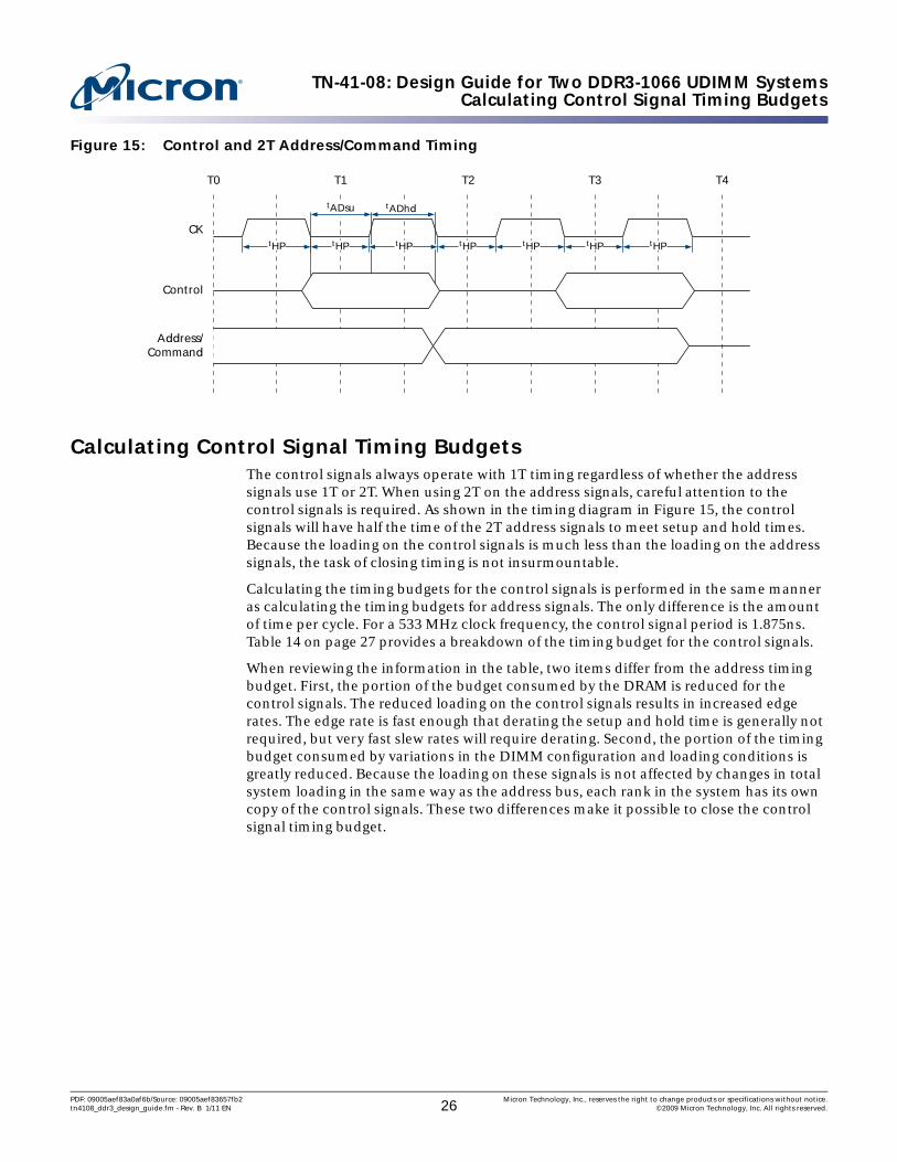
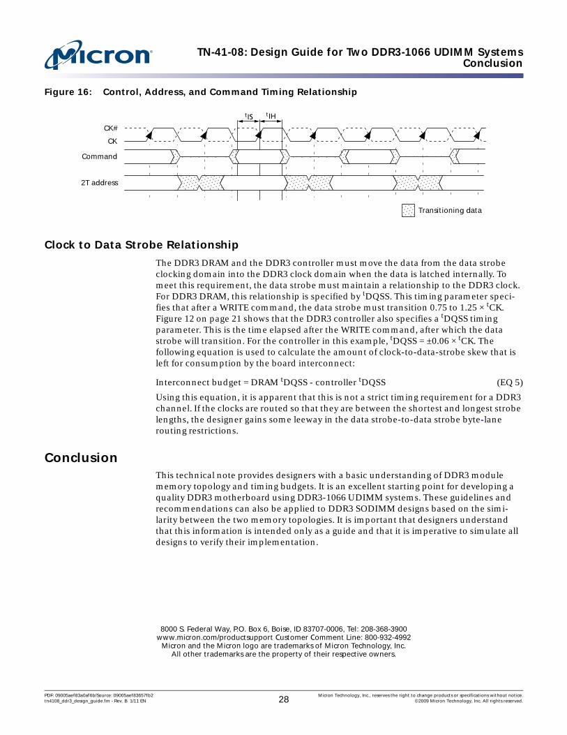
Figure 15: Control and 2T Address/Command Timing
Calculating Control Signal Timing BudgetsThe control signals always operate with 1T timing regardless of whether the address signals use 1T or 2T. When using 2T on the address signals, careful attention to the control signals is required. As shown in the timing diagram in Figure 15, the control signals will have half the time of the 2T address signals to meet setup and hold times. Because the loading on the control signals is much less than the loading on the address signals, the task of closing timing is not insurmountable.
Calculating the timing budgets for the control signals is performed in the same manner as calculating the timing budgets for address signals. The only difference is the amount of time per cycle. For a 533 MHz clock frequency, the control signal period is 1.875ns. Table 14 on page 27 provides a breakdown of the timing budget for the control signals.
When reviewing the information in the table, two items differ from the address timing budget. First, the portion of the budget consumed by the DRAM is reduced for the control signals. The reduced loading on the control signals results in increased edge rates. The edge rate is fast enough that derating the setup and hold time is generally not required, but very fast slew rates will require derating. Second, the portion of the timing budget consumed by variations in the DIMM configuration and loading conditions is greatly reduced. Because the loading on these signals is not affected by changes in total system loading in the same way as the address bus, each rank in the system has its own copy of the control signals. These two differences make it possible to close the control signal timing budget.
CK
T0 T1 T2 T3 T4
Control
Address/Command
tADsu tADhd
tHPtHPtHPtHPtHPtHPtHP
PDF: 09005aef83a0af6b/Source: 09005aef83657fb2 Micron Technology, Inc., reserves the right to change products or specifications without notice.tn4108_ddr3_design_guide.fm - Rev. B 1/11 EN 26 ©2009 Micron Technology, Inc. All rights reserved.
TN-41-08: Design Guide for Two DDR3-1066 UDIMM SystemsCalculating Control Signal Timing Budgets
Notes: 1. These are worst-case slow numbers (95°C, 1.7V, slow process).
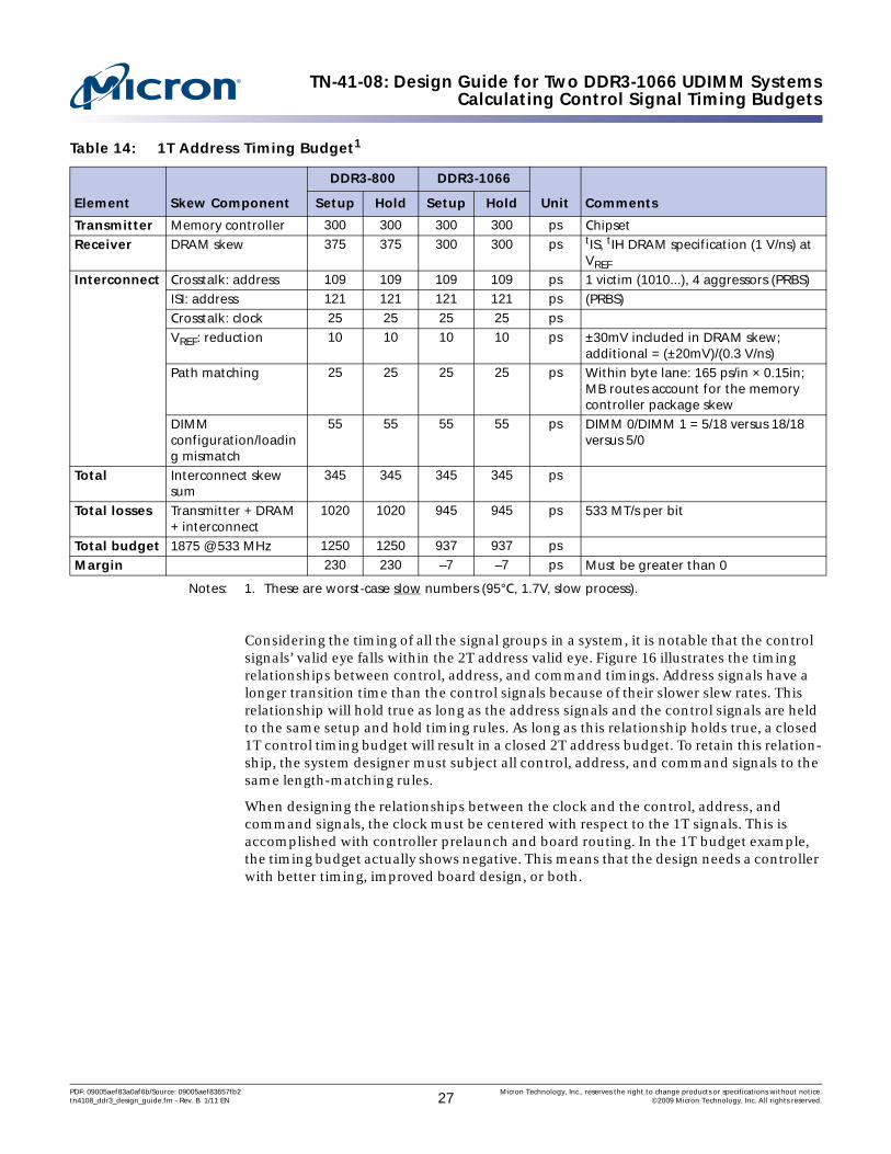
Considering the timing of all the signal groups in a system, it is notable that the control signals’ valid eye falls within the 2T address valid eye. Figure 16 illustrates the timing relationships between control, address, and command timings. Address signals have a longer transition time than the control signals because of their slower slew rates. This relationship will hold true as long as the address signals and the control signals are held to the same setup and hold timing rules. As long as this relationship holds true, a closed 1T control timing budget will result in a closed 2T address budget. To retain this relation-ship, the system designer must subject all control, address, and command signals to the same length-matching rules.
When designing the relationships between the clock and the control, address, and command signals, the clock must be centered with respect to the 1T signals. This is accomplished with controller prelaunch and board routing. In the 1T budget example, the timing budget actually shows negative. This means that the design needs a controller with better timing, improved board design, or both.
Table 14: 1T Address Timing Budget1
Element Skew Component
DDR3-800 DDR3-1066
Unit CommentsSetup Hold Setup Hold
Transmitter Memory controller 300 300 300 300 ps ChipsetReceiver DRAM skew 375 375 300 300 ps tIS, tIH DRAM specification (1 V/ns) at
VREF
Interconnect Crosstalk: address 109 109 109 109 ps 1 victim (1010...), 4 aggressors (PRBS)ISI: address 121 121 121 121 ps (PRBS)Crosstalk: clock 25 25 25 25 ps
VREF: reduction 10 10 10 10 ps ±30mV included in DRAM skew; additional = (±20mV)/(0.3 V/ns)
Path matching 25 25 25 25 ps Within byte lane: 165 ps/in × 0.15in; MB routes account for the memory controller package skew
DIMM configuration/loading mismatch
55 55 55 55 ps DIMM 0/DIMM 1 = 5/18 versus 18/18 versus 5/0
Total Interconnect skew sum
345 345 345 345 ps
Total losses Transmitter + DRAM + interconnect
1020 1020 945 945 ps 533 MT/s per bit
Total budget 1875 @ 533 MHz 1250 1250 937 937 ps
Margin 230 230 –7 –7 ps Must be greater than 0
PDF: 09005aef83a0af6b/Source: 09005aef83657fb2 Micron Technology, Inc., reserves the right to change products or specifications without notice.tn4108_ddr3_design_guide.fm - Rev. B 1/11 EN 27 ©2009 Micron Technology, Inc. All rights reserved.
TN-41-08: Design Guide for Two DDR3-1066 UDIMM SystemsConclusion
Figure 16: Control, Address, and Command Timing Relationship
Clock to Data Strobe Relationship
The DDR3 DRAM and the DDR3 controller must move the data from the data strobe clocking domain into the DDR3 clock domain when the data is latched internally. To meet this requirement, the data strobe must maintain a relationship to the DDR3 clock. For DDR3 DRAM, this relationship is specified by tDQSS. This timing parameter speci-fies that after a WRITE command, the data strobe must transition 0.75 to 1.25 × tCK. Figure 12 on page 21 shows that the DDR3 controller also specifies a tDQSS timing parameter. This is the time elapsed after the WRITE command, after which the data strobe will transition. For the controller in this example, tDQSS = ±0.06 × tCK. The following equation is used to calculate the amount of clock-to-data-strobe skew that is left for consumption by the board interconnect:
Interconnect budget = DRAM tDQSS - controller tDQSS (EQ 5)
Using this equation, it is apparent that this is not a strict timing requirement for a DDR3 channel. If the clocks are routed so that they are between the shortest and longest strobe lengths, the designer gains some leeway in the data strobe-to-data strobe byte-lane routing restrictions.
ConclusionThis technical note provides designers with a basic understanding of DDR3 module memory topology and timing budgets. It is an excellent starting point for developing a quality DDR3 motherboard using DDR3-1066 UDIMM systems. These guidelines and recommendations can also be applied to DDR3 SODIMM designs based on the simi-larity between the two memory topologies. It is important that designers understand that this information is intended only as a guide and that it is imperative to simulate all designs to verify their implementation.
CK
CK#
Command
2T address
Transitioning data
tIS tIH
8000 S. Federal Way, P.O. Box 6, Boise, ID 83707-0006, Tel: 208-368-3900www.micron.com/productsupport Customer Comment Line: 800-932-4992
Micron and the Micron logo are trademarks of Micron Technology, Inc. All other trademarks are the property of their respective owners.
PDF: 09005aef83a0af6b/Source: 09005aef83657fb2 Micron Technology, Inc., reserves the right to change products or specifications without notice.tn4108_ddr3_design_guide.fm - Rev. B 1/11 EN 28 ©2009 Micron Technology, Inc. All rights reserved.
TN-41-08: Design Guide for Two DDR3-1066 UDIMM SystemsRevision History
Revision HistoryRev. B . . . . . . . . . . . . . . . . . . . . . . . . . . . . . . . . . . . . . . . . . . . . . . . . . . . . . . . . . . . . . . . . . . . . . . . . . . . . . . . . . . . . . . . . . . . . . . . 1/11
• Updated formats, added values, and revised text for clarity.
Rev. A . . . . . . . . . . . . . . . . . . . . . . . . . . . . . . . . . . . . . . . . . . . . . . . . . . . . . . . . . . . . . . . . . . . . . . . . . . . . . . . . . . . . . . . . . . . . . . . 5/09• Initial release.
8000 S. Federal Way, P.O. Box 6, Boise, ID 83707-0006, Tel: 208-368-3900www.micron.com/productsupport Customer Comment Line: 800-932-4992
Micron and the Micron logo are trademarks of Micron Technology, Inc. All other trademarks are the property of their respective owners.
PDF: 09005aef83a0af6b/Source: 09005aef83657fb2 Micron Technology, Inc., reserves the right to change products or specifications without notice.tn4108_ddr3_design_guide.fm - Rev. B 1/11 EN 29 ©2009 Micron Technology, Inc. All rights reserved.