Embed Size (px)
Citation preview
Product
Folder
Order
Now
Technical
Documents
Tools &
Software
Support &Community
An IMPORTANT NOTICE at the end of this data sheet addresses availability, warranty, changes, use in safety-critical applications,intellectual property matters and other important disclaimers. PRODUCTION DATA.
TMS320F28379D, TMS320F28378D, TMS320F28377DTMS320F28376D, TMS320F28375D, TMS320F28374D
SPRS880M –DECEMBER 2013–REVISED JUNE 2020
TMS320F2837xD Dual-Core Microcontrollers
1 Device Overview
1
1.1 Features1
• Dual-core architecture– Two TMS320C28x 32-bit CPUs– 200 MHz– IEEE 754 single-precision Floating-Point Unit
(FPU)– Trigonometric Math Unit (TMU)– Viterbi/Complex Math Unit (VCU-II)
• Two programmable Control Law Accelerators(CLAs)– 200 MHz– IEEE 754 single-precision floating-point
instructions– Executes code independently of main CPU
• On-chip memory– 512KB (256KW) or 1MB (512KW) of flash
(ECC-protected)– 172KB (86KW) or 204KB (102KW) of RAM
(ECC-protected or parity-protected)– Dual-zone security supporting third-party
development– Unique identification number
• Clock and system control– Two internal zero-pin 10-MHz oscillators– On-chip crystal oscillator– Windowed watchdog timer module– Missing clock detection circuitry
• 1.2-V core, 3.3-V I/O design• System peripherals
– Two External Memory Interfaces (EMIFs) withASRAM and SDRAM support
– Dual 6-channel Direct Memory Access (DMA)controllers
– Up to 169 individually programmable,multiplexed General-Purpose Input/Output(GPIO) pins with input filtering
– Expanded Peripheral Interrupt controller (ePIE)– Multiple Low-Power Mode (LPM) support with
external wakeup• Communications peripherals
– USB 2.0 (MAC + PHY)– Support for 12-pin 3.3 V-compatible Universal
Parallel Port (uPP) interface– Two Controller Area Network (CAN) modules
(pin-bootable)– Three high-speed (up to 50-MHz) SPI ports (pin-
bootable)
– Two Multichannel Buffered Serial Ports(McBSPs)
– Four Serial Communications Interfaces(SCI/UART) (pin-bootable)
– Two I2C interfaces (pin-bootable)• Analog subsystem
– Up to four Analog-to-Digital Converters (ADCs)– 16-bit mode
– 1.1 MSPS each (up to 4.4-MSPS systemthroughput)
– Differential inputs– Up to 12 external channels
– 12-bit mode– 3.5 MSPS each (up to 14-MSPS system
throughput)– Single-ended inputs– Up to 24 external channels
– Single Sample-and-Hold (S/H) on each ADC– Hardware-integrated post-processing of ADC
conversions– Saturating offset calibration– Error from setpoint calculation– High, low, and zero-crossing compare,
with interrupt capability– Trigger-to-sample delay capture
– Eight windowed comparators with 12-bit Digital-to-Analog Converter (DAC) references
– Three 12-bit buffered DAC outputs• Enhanced control peripherals
– 24 Pulse Width Modulator (PWM) channels withenhanced features
– 16 High-Resolution Pulse Width Modulator(HRPWM) channels– High resolution on both A and B channels of
8 PWM modules– Dead-band support (on both standard and
high resolution)– Six Enhanced Capture (eCAP) modules– Three Enhanced Quadrature Encoder Pulse
(eQEP) modules– Eight Sigma-Delta Filter Module (SDFM) input
channels, 2 parallel filters per channel– Standard SDFM data filtering– Comparator filter for fast action for out of
range
2
TMS320F28379D, TMS320F28378D, TMS320F28377DTMS320F28376D, TMS320F28375D, TMS320F28374DSPRS880M –DECEMBER 2013–REVISED JUNE 2020 www.ti.com
Submit Documentation FeedbackProduct Folder Links: TMS320F28379D TMS320F28378D TMS320F28377D TMS320F28376D TMS320F28375D
TMS320F28374D
Device Overview Copyright © 2013–2020, Texas Instruments Incorporated
• Configurable Logic Block (CLB)– Augments existing peripheral capability– Supports position manager solutions
• Functional Safety-Compliant– Developed for functional safety applications– Documentation available to aid ISO 26262
system design up to ASIL D; IEC 61508 up toSIL 3; IEC 60730 up to Class C; and UL 1998up to Class 2
– Hardware integrity up to ASIL B, SIL 2• Safety-related certification
– ISO 26262 certified up to ASIL B and IEC 61508certified up to SIL 2 by TUV SUD
• Package options:– Lead-free, green packaging– 337-ball New Fine Pitch Ball Grid Array
(nFBGA) [ZWT suffix]– 176-pin PowerPAD™ Thermally Enhanced Low-
Profile Quad Flatpack (HLQFP) [PTP suffix]– 100-pin PowerPAD Thermally Enhanced Thin
Quad Flatpack (HTQFP) [PZP suffix]• Temperature options:
– T: –40ºC to 105ºC junction– S: –40ºC to 125ºC junction– Q: –40ºC to 125ºC free-air
(AEC Q100 qualification for automotiveapplications)
1.2 Applications• Medium/short range radar• Traction inverter motor control• HVAC large commercial motor control• Automated sorting equipment• CNC control• AC charging (pile) station• DC charging (pile) station• EV charging station power module• Energy storage power conversion system (PCS)• Central inverter
• Solar power optimizer• String inverter• Inverter & motor control• On-board (OBC) & wireless charger• Linear motor segment controller• Servo drive control module• AC-input BLDC motor drive• DC-input BLDC motor drive• Industrial AC-DC• Three phase UPS
1.3 DescriptionC2000™ 32-bit microcontrollers are optimized for processing, sensing, and actuation to improve closed-loop performance in real-time control applications such as industrial motor drives; solar inverters anddigital power; electrical vehicles and transportation; motor control; and sensing and signal processing. TheC2000 line includes the Premium performance MCUs and the Entry performance MCUs.
The TMS320F2837xD is a powerful 32-bit floating-point microcontroller unit (MCU) designed for advancedclosed-loop control applications such as industrial motor drives; solar inverters and digital power; electricalvehicles and transportation; and sensing and signal processing. To accelerate application development,the DigitalPower software development kit (SDK) for C2000 MCUs and the MotorControl softwaredevelopment kit (SDK) for C2000™ MCUs are available. The F2837xD supports a new dual-core C28xarchitecture that significantly boosts system performance. The integrated analog and control peripheralsalso let designers consolidate control architectures and eliminate multiprocessor use in high-end systems.
The dual real-time control subsystems are based on TI’s 32-bit C28x floating-point CPUs, which provide200 MHz of signal processing performance in each core. The C28x CPUs are further boosted by the newTMU accelerator, which enables fast execution of algorithms with trigonometric operations common intransforms and torque loop calculations; and the VCU accelerator, which reduces the time for complexmath operations common in encoded applications.

3
TMS320F28379D, TMS320F28378D, TMS320F28377DTMS320F28376D, TMS320F28375D, TMS320F28374D
www.ti.com SPRS880M –DECEMBER 2013–REVISED JUNE 2020
Submit Documentation FeedbackProduct Folder Links: TMS320F28379D TMS320F28378D TMS320F28377D TMS320F28376D TMS320F28375D
TMS320F28374D
Device OverviewCopyright © 2013–2020, Texas Instruments Incorporated
The F2837xD microcontroller family features two CLA real-time control coprocessors. The CLA is anindependent 32-bit floating-point processor that runs at the same speed as the main CPU. The CLAresponds to peripheral triggers and executes code concurrently with the main C28x CPU. This parallelprocessing capability can effectively double the computational performance of a real-time control system.By using the CLA to service time-critical functions, the main C28x CPU is free to perform other tasks, suchas communications and diagnostics. The dual C28x+CLA architecture enables intelligent partitioningbetween various system tasks. For example, one C28x+CLA core can be used to track speed andposition, while the other C28x+CLA core can be used to control torque and current loops.
The TMS320F2837xD supports up to 1MB (512KW) of onboard flash memory with error correction code(ECC) and up to 204KB (102KW) of SRAM. Two 128-bit secure zones are also available on each CPU forcode protection.
Performance analog and control peripherals are also integrated on the F2837xD MCU to further enablesystem consolidation. Four independent 16-bit ADCs provide precise and efficient management of multipleanalog signals, which ultimately boosts system throughput. The new sigma-delta filter module (SDFM)works in conjunction with the sigma-delta modulator to enable isolated current shunt measurements. TheComparator Subsystem (CMPSS) with windowed comparators allows for protection of power stages whencurrent limit conditions are exceeded or not met. Other analog and control peripherals include DACs,PWMs, eCAPs, eQEPs, and other peripherals.
Peripherals such as EMIFs, CAN modules (ISO 11898-1/CAN 2.0B-compliant), and a new uPP interfaceextend the connectivity of the F2837xD. The uPP interface is a new feature of the C2000™ MCUs andsupports high-speed parallel connection to FPGAs or other processors with similar uPP interfaces. Lastly,a USB 2.0 port with MAC and PHY lets users easily add universal serial bus (USB) connectivity to theirapplication.
To learn more about the C2000 MCUs, visit the C2000 Overview at www.ti.com/c2000.
(1) For more information on these devices, see Mechanical, Packaging, and Orderable Information.
Device Information (1)
PART NUMBER PACKAGE BODY SIZETMS320F28379DZWT nFBGA (337) 16.0 mm × 16.0 mmTMS320F28377DZWT nFBGA (337) 16.0 mm × 16.0 mmTMS320F28376DZWT nFBGA (337) 16.0 mm × 16.0 mmTMS320F28375DZWT nFBGA (337) 16.0 mm × 16.0 mmTMS320F28374DZWT nFBGA (337) 16.0 mm × 16.0 mmTMS320F28379DPTP HLQFP (176) 24.0 mm × 24.0 mmTMS320F28378DPTP HLQFP (176) 24.0 mm × 24.0 mmTMS320F28377DPTP HLQFP (176) 24.0 mm × 24.0 mmTMS320F28376DPTP HLQFP (176) 24.0 mm × 24.0 mmTMS320F28375DPTP HLQFP (176) 24.0 mm × 24.0 mmTMS320F28374DPTP HLQFP (176) 24.0 mm × 24.0 mmTMS320F28375DPZP HTQFP (100) 14.0 mm × 14.0 mm

16-/12-bit ADC
x4
Analog
MUX
ADC
Result
Regs
Peripheral Frame 1
Global Shared
16x 4Kx16
GS0-GS15 RAMs
CPU1 to CPU2
1Kx16 MSG RAM
GPIO MUX, Input X-BAR, Output X-BAR
CPU1.M0 RAM 1Kx16
CPU1.M1 RAM 1Kx16
CPU2.M0 RAM 1Kx16
CPU2.M1 RAM 1Kx16
PSWDPSWD
Secure Memories
shown in Red
MEMCPU2
CPU2 to CPU1
1Kx16 MSG RAM
MEMCPU1
CPU1 Buses
CPU2 Buses
A5:0
B5:0
C5:2
ADCIN14
ADCIN15
D5:0
Comparator
Subsystem
(CMPSS)
DAC
x3
Config
CP
U1
.CL
A1
Bu
s
CP
U2
.CL
A1
Bu
s
C28 CPU-1FPU
VCU-II
TMU
CPU Timer 0
CPU Timer 1
CPU Timer 2
ePIE(up to 192
interrupts)
WD Timer
NMI-WDT
C28 CPU-2FPU
VCU-II
TMU
CPU Timer 0
CPU Timer 1
CPU Timer 2
ePIE(up to 192
interrupts)
WD Timer
NMI-WDTCPU1.CLA1 Data ROM
(4Kx16)
CPU1.CLA1 to CPU1
128x16 MSG RAM
CPU1 to CPU1.CLA1
128x16 MSG RAM
CPU1.D0 RAM 2Kx16
CPU1.D1 RAM 2Kx16
Boot-ROM 32Kx16
Nonsecure
Secure-ROM 32Kx16
Secure
CPU1 Local Shared
6x 2Kx16
LS0-LS5 RAMs
CPU2 to CPU2.CLA1
128x16 MSG RAM
CPU2.CLA1 to CPU2
128x16 MSG RAM
CPU2.D0 RAM 2Kx16
CPU2.D1 RAM 2Kx16
CPU2.CLA1 Data ROM
(4Kx16)
Boot-ROM 32Kx16
Nonsecure
Secure-ROM 32Kx16
Secure
CPU2 Local Shared
LS0-LS5 RAMs
CPU1.CLA1
CPU1.DMA CPU2.DMA
CPU2.CLA1
Data BusBridge
ePWM-1/../12eCAP-
1/../6eQEP-1/2/3 SDFM-1/2
EX
TS
YN
CIN
EX
TS
YN
CO
UT
TZ
1-T
Z6
EC
AP
x
EQ
EP
xA
EQ
EP
xB
EP
WM
xA
EP
WM
xB
EQ
EP
xI
EQ
EP
xS
SD
x_
Dy
SD
x_
Cy
A
B
C
D
JTAG
AUXCLKIN
External Crystal orOscillator
Watchdog 1/2
Main PLL
Aux PLL
INTOSC1
INTOSC2
Low-PowerMode Control
GPIO MUX
TRST
TCK
TDI
TMS
TDO
6x 2Kx16
DualCode
SecurityModule
+Emulation
CodeSecurity
Logic(ECSL)
DualCode
SecurityModule
+Emulation
CodeSecurity
Logic(ECSL)
InterprocessorCommunication
(IPC)Module
PUMP
OTP/Flash
Wrapper
FLASH256K x 16
Secure
UserConfigurable
DCSMOTP
1K x 16
OTP/Flash
Wrapper
FLASH256K x 16
Secure
UserConfigurable
DCSMOTP
1K x 16
SCI-
A/B/C/D
(16L FIFO)
I2C-A/B
(16L FIFO)
Data Bus Bridge
SC
ITX
Dx
SC
IRX
Dx
SD
Ax
SC
Lx
CAN-
A/B(32-MBOX)
Data BusBridge
CA
NR
Xx
CA
NT
Xx
GPIO
Data BusBridge
GP
IOn
Data BusBridge
USB
Ctrl /
PHY
US
BD
P
US
BD
M
USB
Ctrl /
PHY
EMIF1
Data BusBridge
EM
1D
x
EM
1A
x
EM
1C
TL
x
EMIF2
Data BusBridge
EM
2D
x
EM
2A
x
EM
2C
TL
x
Peripheral Frame 2
SPI-
A/B/C
(16L FIFO)
SP
ISIM
Ox
SP
ISO
MIx
SP
ICL
Kx
SP
IST
Ex
McBSP-
A/B
MD
Xx
MD
Rx
MC
LK
Xx
MC
LK
Rx
MF
SX
x
MF
SR
x
uPPRAM
UP
PA
D[7
:0]
UP
PA
EN
UP
PA
ST
UP
PA
WT
UP
PA
CL
K
HRPWM-1/../8(CPU1 only)
4
TMS320F28379D, TMS320F28378D, TMS320F28377DTMS320F28376D, TMS320F28375D, TMS320F28374DSPRS880M –DECEMBER 2013–REVISED JUNE 2020 www.ti.com
Submit Documentation FeedbackProduct Folder Links: TMS320F28379D TMS320F28378D TMS320F28377D TMS320F28376D TMS320F28375D
TMS320F28374D
Device Overview Copyright © 2013–2020, Texas Instruments Incorporated
1.4 Functional Block DiagramFigure 1-1 shows the CPU system and associated peripherals.
Figure 1-1. Functional Block Diagram
5
TMS320F28379D, TMS320F28378D, TMS320F28377DTMS320F28376D, TMS320F28375D, TMS320F28374D
www.ti.com SPRS880M –DECEMBER 2013–REVISED JUNE 2020
Submit Documentation FeedbackProduct Folder Links: TMS320F28379D TMS320F28378D TMS320F28377D TMS320F28376D TMS320F28375D
TMS320F28374D
Table of ContentsCopyright © 2013–2020, Texas Instruments Incorporated
Table of Contents1 Device Overview ......................................... 1
1.1 Features .............................................. 11.2 Applications........................................... 21.3 Description............................................ 21.4 Functional Block Diagram ........................... 4
2 Revision History ......................................... 63 Device Comparison ..................................... 9
3.1 Related Products.................................... 114 Terminal Configuration and Functions ............ 12
4.1 Pin Diagrams........................................ 124.2 Signal Descriptions.................................. 194.3 Pins With Internal Pullup and Pulldown............. 424.4 Pin Multiplexing...................................... 434.5 Connections for Unused Pins ....................... 50
5 Specifications ........................................... 515.1 Absolute Maximum Ratings ........................ 515.2 ESD Ratings – Commercial ......................... 525.3 ESD Ratings – Automotive.......................... 525.4 Recommended Operating Conditions............... 535.5 Power Consumption Summary...................... 545.6 Electrical Characteristics ............................ 585.7 Thermal Resistance Characteristics ................ 595.8 Thermal Design Considerations .................... 605.9 System .............................................. 615.10 Analog Peripherals .................................. 975.11 Control Peripherals ................................ 1275.12 Communications Peripherals ...................... 146
6 Detailed Description.................................. 1806.1 Overview ........................................... 1806.2 Functional Block Diagram ......................... 180
6.3 Memory ............................................ 1826.4 Identification........................................ 1906.5 Bus Architecture – Peripheral Connectivity........ 1916.6 C28x Processor .................................... 1926.7 Control Law Accelerator ........................... 1956.8 Direct Memory Access............................. 1966.9 Interprocessor Communication Module............ 1986.10 Boot ROM and Peripheral Booting................. 1996.11 Dual Code Security Module ....................... 2026.12 Timers.............................................. 2036.13 Nonmaskable Interrupt With Watchdog Timer
(NMIWD) ........................................... 2036.14 Watchdog .......................................... 2046.15 Configurable Logic Block (CLB) ................... 2056.16 Functional Safety .................................. 207
7 Applications, Implementation, and Layout ...... 2097.1 TI Reference Design............................... 209
8 Device and Documentation Support .............. 2108.1 Device and Development Support Tool
Nomenclature ...................................... 2108.2 Markings ........................................... 2118.3 Tools and Software ................................ 2128.4 Documentation Support............................ 2148.5 Related Links ...................................... 2158.6 Support Resources ................................ 2158.7 Trademarks ........................................ 2158.8 Electrostatic Discharge Caution ................... 2158.9 Glossary............................................ 215
9 Mechanical, Packaging, and OrderableInformation ............................................. 2169.1 Packaging Information ............................. 216

6
TMS320F28379D, TMS320F28378D, TMS320F28377DTMS320F28376D, TMS320F28375D, TMS320F28374DSPRS880M –DECEMBER 2013–REVISED JUNE 2020 www.ti.com
Submit Documentation FeedbackProduct Folder Links: TMS320F28379D TMS320F28378D TMS320F28377D TMS320F28376D TMS320F28375D
TMS320F28374D
Revision History Copyright © 2013–2020, Texas Instruments Incorporated
2 Revision History
Changes from March 3, 2020 to June 25, 2020 (from L Revision (March 2020) to M Revision) Page
• Global: Changed "debug probe" to "JTAG debug probe"....................................................................... 1• Section 1.1 (Features): Updated "Functional Safety-Compliant" feature. Added "Safety-related certification" feature.. 1• Section 5.1 (Absolute Maximum Ratings): Updated Input clamp current. .................................................. 51• Table 5-4 (Reset (XRS) Timing Requirements): Updated tw(RSL2). ............................................................ 62• Section 5.11.5.1 (SDFM Electrical Data and Timing (Using ASYNC)): Added WARNING about Mode 2
(Manchester Mode). ............................................................................................................... 142• Table 5-67 (SDFM Timing Requirements When Using Asynchronous GPIO (ASYNC) Option): Added four
parameters to Mode 2 section. .................................................................................................. 142• Figure 5-58 (SDFM Timing Diagram – Mode 2): Updated figure. .......................................................... 144• Section 5.12.2.1 (I2C Electrical Data and Timing): Updated NOTE about I2C module clock. .......................... 150• Table 5-69 (I2C Timing Requirements): Updated table. ..................................................................... 150• Table 5-70 (I2C Switching Characteristics): Updated table. ................................................................. 150• Figure 5-62 (I2C Timing Diagram): Added figure. ............................................................................ 151• Figure 5-70 (SCI Block Diagram): Updated figure. ............................................................................ 163• Figure 5-73 (SPI Master Mode External Timing (Clock Phase = 1)): Updated Parameter 24. .......................... 170• Table 5-80 (SPI Slave Mode Timing Requirements): Updated Parameter 25, tsu(STE)S. ................................. 171• Table 6-5 (Peripheral Registers Memory Map): Added footnote about address overlap of PieCtrlRegs and
Cla1SoftIntRegs. ................................................................................................................... 185• Section 6.16 (Functional Safety): Updated section. .......................................................................... 207
7
TMS320F28379D, TMS320F28378D, TMS320F28377DTMS320F28376D, TMS320F28375D, TMS320F28374D
www.ti.com SPRS880M –DECEMBER 2013–REVISED JUNE 2020
Submit Documentation FeedbackProduct Folder Links: TMS320F28379D TMS320F28378D TMS320F28377D TMS320F28376D TMS320F28375D
TMS320F28374D
Revision HistoryCopyright © 2013–2020, Texas Instruments Incorporated
Changes from November 16, 2018 to March 2, 2020 (from K Revision (November 2018) to L Revision) Page
• Section 1.1 (Features): Added "Functional Safety Compliant" feature. ....................................................... 1• Section 1.2 (Applications): Updated section. ..................................................................................... 2• Section 1.3 (Description): Updated section. ...................................................................................... 2• Figure 1-1 (Functional Block Diagram): Changed MRXx to MDRx. ........................................................... 4• Table 3-1 (Device Comparison): Added number of CLB tiles. ................................................................. 9• Table 3-1: Changed availability of TMS320F28379D (PTP) in "Q" temperature range to "Yes". ......................... 9• Section 5.1 (Absolute Maximum Ratings): Changed "Input clamp current" condition from "Digital input (per
pin), ..." to "Digital/analog input (per pin), ...". .................................................................................. 51• Section 5.1: Added footnote about continuous clamp current. ................................................................ 51• Section 5.2 (ESD Ratings – Commercial): Added ANSI/ESDA/JEDEC JS-002 to charged-device model (CDM) ..... 52• Section 5.5.2 (Reducing Current Consumption): Updated list of methods for reducing the device current
consumption.......................................................................................................................... 57• Section 5.6 (Electrical Characteristics): Added VDDIO-POR parameter. ........................................................ 58• Section 5.9.1.5 (Supply Supervision): Added NOTE. .......................................................................... 61• Table 5-7 (Input Clock Frequency): Updated f(X1). .............................................................................. 66• Section 5.9.5 (Emulation/JTAG): Changed "emulator" to "debug probe". .................................................. 72• Table 5-38 (EMIF Asynchronous Memory Switching Characteristics): Updated Parameter 3 [tc(EMRCYCLE)] and
Parameter 15 [tc(EMWCYCLE)]. ........................................................................................................ 90• Section 5.10 (Analog Peripheral): Updated feature about buffered DACs. ................................................. 97• Figure 5-29 (Analog Subsystem Block Diagram (100-Pin PZP)): Updated ADC-A and ADC-B blocks by changing
"16-bits or 12-bits (selectable)" to "12-bits". ................................................................................... 100• Section 5.10.1.2 (ADC Electrical Data and Timing): Added NOTE about keeping VREFHI pin below VDDA + 0.3 V
to ensure proper functional operation. .......................................................................................... 105• Table 5-51 (ADC Timings in 12-Bit Mode (SYSCLK Cycles)): Added footnote. .......................................... 112• Table 5-52 (ADC Timings in 16-Bit Mode): Added footnote. ................................................................ 114• Table 5-54 (Comparator Electrical Characteristics): Updated description of "Power-up time" parameter. ............ 119• Table 5-54: Changed MAX Power-up time from 10 µs to 500 µs. Added footnote referencing the "Analog
Bandgap References" advisory. ................................................................................................. 119• Table 5-54: Added TEST CONDITION for "Input referred offset error"..................................................... 119• Table 5-54: Added Common Mode Rejection Ratio (CMRR). ............................................................... 119• Table 5-55 (CMPSS DAC Static Electrical Characteristics): Added footnote about maximum output voltage. ...... 121• Section 5.10.3 (Buffered Digital-to-Analog Converter (DAC)): Updated section. ......................................... 123• Figure 5-44 (DAC Module Block Diagram): Updated figure. ................................................................ 123• Section 5.10.3.1 (Buffered DAC Electrical Data and Timing): Added NOTE about keeping VREFHI pin below VDDA
+ 0.3 V to ensure proper functional operation.................................................................................. 124• Table 5-56 (Buffered DAC Electrical Characteristics): Updated description of "Power-up time" parameter. .......... 124• Table 5-56: Changed MAX Power-up time from 10 µs to 500 µs. Added footnote referencing the "Analog
Bandgap References" advisory. ................................................................................................. 124• Table 5-56: Changed "Trimmed offset error" to "Offset error". .............................................................. 124• Table 5-56: Added TYP DNL value.............................................................................................. 124• Table 5-56: Added TYP INL value. .............................................................................................. 124• Table 5-56: Changed description of RPD to "RPD pulldown resistor"......................................................... 124• Table 5-56: Changed "Reference load" to "Reference input resistance". .................................................. 124• Table 5-56: Updated footnote about typical values............................................................................ 124• Table 5-59 (ePWM Timing Requirements): Added f(EPWM) and associated footnote. .................................... 134• Table 5-65 (High-Resolution PWM Timing Requirements): Added table. ................................................. 139• Section 5.11.5.2 (SDFM Electrical Data and Timing (Using 3-Sample GPIO Input Qualification)): Updated NOTE
about the SDFM Qualified GPIO (3-sample) mode. .......................................................................... 145• Section 5.12.3.1.2 (McBSP as SPI Master or Slave Timing): Updated section. .......................................... 157• Figure 5-66 (McBSP Timing as SPI Master or Slave: CLKSTP = 10b, CLKXP = 0): Updated M28. Added M26. ... 160• Figure 5-67 (McBSP Timing as SPI Master or Slave: CLKSTP = 11b, CLKXP = 0): Added M36. .................... 160• Figure 5-68 (McBSP Timing as SPI Master or Slave: CLKSTP = 10b, CLKXP = 1): Updated M47. Added M45. ... 161• Section 5.12.5.1 (SPI Electrical Data and Timing): Updated section. ...................................................... 167• Table 5-77 (SPI Master Mode Timing Requirements): Updated table. .................................................... 167• Table 5-78 (SPI Master Mode Switching Characteristics (Clock Phase = 0)): Updated table. ......................... 167• Table 5-79 (SPI Master Mode Switching Characteristics (Clock Phase = 1)): Updated table. ......................... 167• Table 5-80 (SPI Slave Mode Timing Requirements): Updated table. ...................................................... 171
8
TMS320F28379D, TMS320F28378D, TMS320F28377DTMS320F28376D, TMS320F28375D, TMS320F28374DSPRS880M –DECEMBER 2013–REVISED JUNE 2020 www.ti.com
Submit Documentation FeedbackProduct Folder Links: TMS320F28379D TMS320F28378D TMS320F28377D TMS320F28376D TMS320F28375D
TMS320F28374D
Revision History Copyright © 2013–2020, Texas Instruments Incorporated
• Table 5-81 (SPI Slave Mode Switching Characteristics): Updated table. ................................................. 171• Figure 5-76 (USB Block Diagram): Removed "USB PHY" label and left arrow that were above "USB FS/LS
PHY". ............................................................................................................................... 173• Figure 6-1 (Functional Block Diagram): Changed MRXx to MDRx. ........................................................ 181• Table 6-1 (C28x Memory Map): Updated CLA ACCESS for UPP TX MSG RAM and UPP RX MSG RAM........... 182• Section 6.3.2 (Flash Memory Map): Updated Addresses of Flash Sectors on CPU1 and CPU2 for F28379D,
F28378D, F28377D and F28375D table. ....................................................................................... 183• Section 6.3.2: Updated Addresses of Flash Sectors on CPU1 and CPU2 for F28376D and F28374D table. ........ 183• Section 6.10.1 (EMU Boot or Emulation Boot): Updated section............................................................ 200• Table 6-15 (GPIO Pins Used by Each Peripheral Bootloader): Updated pin associations for GPIO28 and
GPIO29. ............................................................................................................................ 201• Section 6.15 (Configurable Logic Block (CLB)): Updated section. ......................................................... 205• Figure 6-6 (CLB Overview): Updated figure. .................................................................................. 206• Section 6.16 (Functional Safety): Added section. ............................................................................ 207• Section 7.1 (TI Reference Design): Changed section title from "TI Design or Reference Design" to "TI Reference
Design". Updated section. ....................................................................................................... 209• Section 8 (Device and Documentation Support): Changed "Community Resources" section to "Support
Resources" section. Updated section. .......................................................................................... 210• Section 8.3 (Tools and Software): Updated section. ......................................................................... 212
9
TMS320F28379D, TMS320F28378D, TMS320F28377DTMS320F28376D, TMS320F28375D, TMS320F28374D
www.ti.com SPRS880M –DECEMBER 2013–REVISED JUNE 2020
Submit Documentation FeedbackProduct Folder Links: TMS320F28379D TMS320F28378D TMS320F28377D TMS320F28376D TMS320F28375D
TMS320F28374D
Device ComparisonCopyright © 2013–2020, Texas Instruments Incorporated
(1) A type change represents a major functional feature difference in a peripheral module. Within a peripheral type, there may be minordifferences between devices that do not affect the basic functionality of the module. For more information, see the C2000 Real-TimeControl Peripherals Reference Guide.
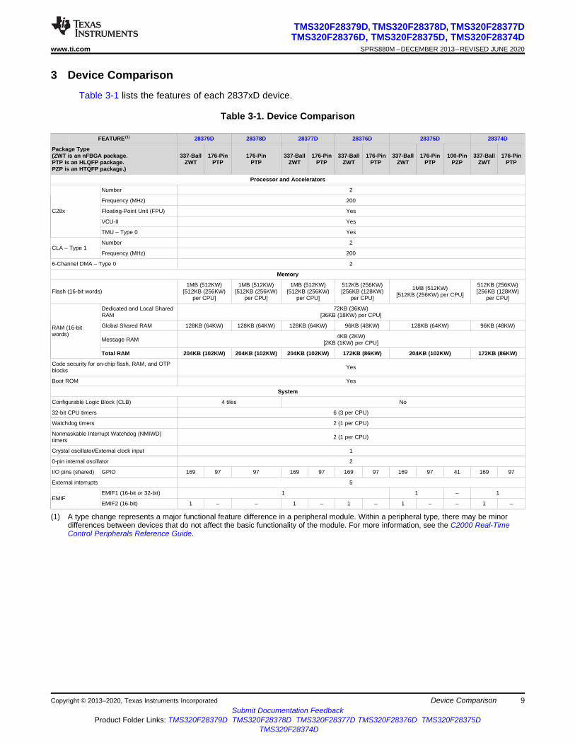
3 Device Comparison
Table 3-1 lists the features of each 2837xD device.
Table 3-1. Device Comparison
FEATURE (1) 28379D 28378D 28377D 28376D 28375D 28374D
Package Type(ZWT is an nFBGA package.PTP is an HLQFP package.PZP is an HTQFP package.)
337-BallZWT
176-PinPTP
176-PinPTP
337-BallZWT
176-PinPTP
337-BallZWT
176-PinPTP
337-BallZWT
176-PinPTP
100-PinPZP
337-BallZWT
176-PinPTP
Processor and Accelerators
C28x
Number 2
Frequency (MHz) 200
Floating-Point Unit (FPU) Yes
VCU-II Yes
TMU – Type 0 Yes
CLA – Type 1Number 2
Frequency (MHz) 200
6-Channel DMA – Type 0 2
Memory
Flash (16-bit words)1MB (512KW)
[512KB (256KW)per CPU]
1MB (512KW)[512KB (256KW)
per CPU]
1MB (512KW)[512KB (256KW)
per CPU]
512KB (256KW)[256KB (128KW)
per CPU]
1MB (512KW)[512KB (256KW) per CPU]
512KB (256KW)[256KB (128KW)
per CPU]
RAM (16-bitwords)
Dedicated and Local SharedRAM
72KB (36KW)[36KB (18KW) per CPU]
Global Shared RAM 128KB (64KW) 128KB (64KW) 128KB (64KW) 96KB (48KW) 128KB (64KW) 96KB (48KW)
Message RAM 4KB (2KW)[2KB (1KW) per CPU]
Total RAM 204KB (102KW) 204KB (102KW) 204KB (102KW) 172KB (86KW) 204KB (102KW) 172KB (86KW)
Code security for on-chip flash, RAM, and OTPblocks Yes
Boot ROM Yes
System
Configurable Logic Block (CLB) 4 tiles No
32-bit CPU timers 6 (3 per CPU)
Watchdog timers 2 (1 per CPU)
Nonmaskable Interrupt Watchdog (NMIWD)timers 2 (1 per CPU)
Crystal oscillator/External clock input 1
0-pin internal oscillator 2
I/O pins (shared) GPIO 169 97 97 169 97 169 97 169 97 41 169 97
External interrupts 5
EMIFEMIF1 (16-bit or 32-bit) 1 1 – 1
EMIF2 (16-bit) 1 – – 1 – 1 – 1 – – 1 –
10
TMS320F28379D, TMS320F28378D, TMS320F28377DTMS320F28376D, TMS320F28375D, TMS320F28374DSPRS880M –DECEMBER 2013–REVISED JUNE 2020 www.ti.com
Submit Documentation FeedbackProduct Folder Links: TMS320F28379D TMS320F28378D TMS320F28377D TMS320F28376D TMS320F28375D
TMS320F28374D
Device Comparison Copyright © 2013–2020, Texas Instruments Incorporated
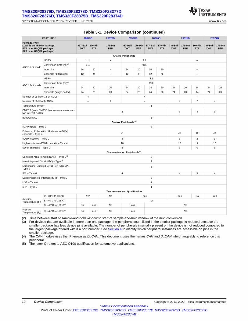
Table 3-1. Device Comparison (continued)FEATURE (1) 28379D 28378D 28377D 28376D 28375D 28374D
Package Type(ZWT is an nFBGA package.PTP is an HLQFP package.PZP is an HTQFP package.)
337-BallZWT
176-PinPTP
176-PinPTP
337-BallZWT
176-PinPTP
337-BallZWT
176-PinPTP
337-BallZWT
176-PinPTP
100-PinPZP
337-BallZWT
176-PinPTP
(2) Time between start of sample-and-hold window to start of sample-and-hold window of the next conversion.(3) For devices that are available in more than one package, the peripheral count listed in the smaller package is reduced because the
smaller package has less device pins available. The number of peripherals internally present on the device is not reduced compared tothe largest package offered within a part number. See Section 4 to identify which peripheral instances are accessible on pins in thesmaller package.
(4) The CAN module uses the IP known as D_CAN. This document uses the names CAN and D_CAN interchangeably to reference thisperipheral.
(5) The letter Q refers to AEC Q100 qualification for automotive applications.
Analog Peripherals
ADC 16-bit mode
MSPS 1.1 – 1.1 –
Conversion Time (ns)(2) 915 – 915 –
Input pins 24 20 – 24 20 24 20 –
Channels (differential) 12 9 – 12 9 12 9 –
ADC 12-bit mode
MSPS 3.5
Conversion Time (ns)(2) 280
Input pins 24 20 20 24 20 24 20 24 20 14 24 20
Channels (single-ended) 24 20 20 24 20 24 20 24 20 14 24 20
Number of 16-bit or 12-bit ADCs 4 – 4 –
Number of 12-bit only ADCs – 4 – 4 2 4
Temperature sensor 1
CMPSS (each CMPSS has two comparators andtwo internal DACs) 8 8 4 8
Buffered DAC 3
Control Peripherals(3)
eCAP inputs – Type 0 6
Enhanced Pulse Width Modulator (ePWM)channels – Type 4 24 24 15 24
eQEP modules – Type 0 3 3 2 3
High-resolution ePWM channels – Type 4 16 16 9 16
SDFM channels – Type 0 8 8 6 8
Communication Peripherals(3)
Controller Area Network (CAN) – Type 0 (4) 2
Inter-Integrated Circuit (I2C) – Type 0 2
Multichannel Buffered Serial Port (McBSP) –Type 1 2
SCI – Type 0 4 4 3 4
Serial Peripheral Interface (SPI) – Type 2 3
USB – Type 0 1
uPP – Type 0 1
Temperature and Qualification
JunctionTemperature (TJ)
T: –40°C to 105°C Yes No Yes Yes No Yes
S: –40°C to 125°C Yes
Q: –40°C to 150°C(5) No Yes No Yes No
Free-AirTemperature (TA) Q: –40°C to 125°C(5) No Yes No Yes No

11
TMS320F28379D, TMS320F28378D, TMS320F28377DTMS320F28376D, TMS320F28375D, TMS320F28374D
www.ti.com SPRS880M –DECEMBER 2013–REVISED JUNE 2020
Submit Documentation FeedbackProduct Folder Links: TMS320F28379D TMS320F28378D TMS320F28377D TMS320F28376D TMS320F28375D
TMS320F28374D
Device ComparisonCopyright © 2013–2020, Texas Instruments Incorporated
3.1 Related ProductsFor information about similar products, see the following links:
TMS320F2837xD MicrocontrollersThe F2837xD series sets a new standard for performance with dual subsystems. Each subsystemconsists of a C28x CPU and a parallel control law accelerator (CLA), each running at 200 MHz. Enhancingperformance are TMU and VCU accelerators. New capabilities include multiple 16-bit/12-bit mode ADCs,DAC, Sigma-Delta filters, USB, configurable logic block (CLB), on-chip oscillators, and enhanced versionsof all peripherals. The F2837xD is available with up to 1MB of Flash. It is available in a 176-pin QFP or337-pin BGA package.
TMS320F2837xS MicrocontrollersThe F2837xS series is a pin-to-pin compatible version of F2837xD but with only one C28x-CPU-and-CLAsubsystem enabled. It is also available in a 100-pin QFP to enable compatibility with the TMS320F2807xseries.
W
V
U
T
R
P
N
M
L
K
10987654321
654321
VSS
VSSA
VSSA
VSSAVSSA
VSSA
VDDA
VDDA
VREFHIB
VREFLOBVREFHID
VREFLOD
VREFHIA
VREFHIC VREFLOA
VREFLOC
W
V
U
TGPIO129GPIO125
GPIO23GPIO24GPIO25GPIO26
GPIO27 GPIO108GPIO107GPIO106
GPIO111GPIO112GPIO110
GPIO109 GPIO114 GPIO113
GPIO122ADCIND4ADCIND2ADCIND0ADCIN14
ADCIN15
ADCINC5ADCINC3
ADCINC2
ADCINA5ADCINA3ADCINA1
ADCINA0 ADCINA2 ADCINA4
ADCINC4
ADCIND1 ADCIND3
ADCINB4ADCINB2ADCINB0
ADCINB1 ADCINB3 ADCINB5
ADCIND5 GPIO123
GPIO124
GPIO126
GPIO127
GPIO128
GPIO130
GPIO131
GPIO116
R
P
VSSVSS
VSSVSSVSS
VDD
VDDVDD
VDDIO
VDDIOVDDIOVDDIO
VDDIO
VDDIO VDD
VSS
VSS
VSS
VSS
VSS
VSS
VSS
VSS
VSS
VSS
VSS
VSS VSS
1098
M
L
K
N
M
L
K
10987
12
TMS320F28379D, TMS320F28378D, TMS320F28377DTMS320F28376D, TMS320F28375D, TMS320F28374DSPRS880M –DECEMBER 2013–REVISED JUNE 2020 www.ti.com
Submit Documentation FeedbackProduct Folder Links: TMS320F28379D TMS320F28378D TMS320F28377D TMS320F28376D TMS320F28375D
TMS320F28374D
Terminal Configuration and Functions Copyright © 2013–2020, Texas Instruments Incorporated
4 Terminal Configuration and Functions
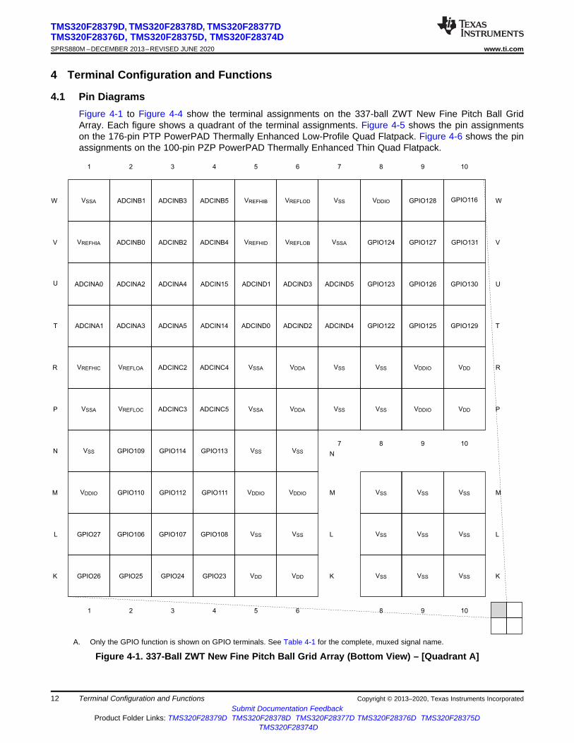
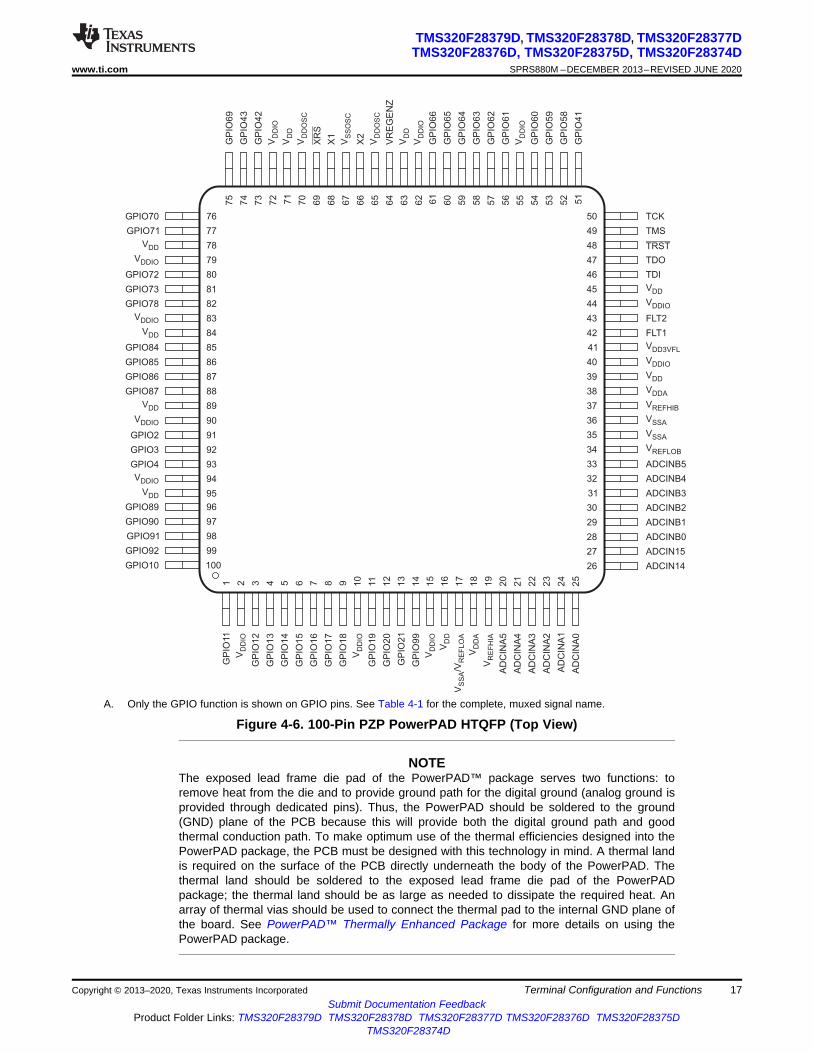
4.1 Pin DiagramsFigure 4-1 to Figure 4-4 show the terminal assignments on the 337-ball ZWT New Fine Pitch Ball GridArray. Each figure shows a quadrant of the terminal assignments. Figure 4-5 shows the pin assignmentson the 176-pin PTP PowerPAD Thermally Enhanced Low-Profile Quad Flatpack. Figure 4-6 shows the pinassignments on the 100-pin PZP PowerPAD Thermally Enhanced Thin Quad Flatpack.
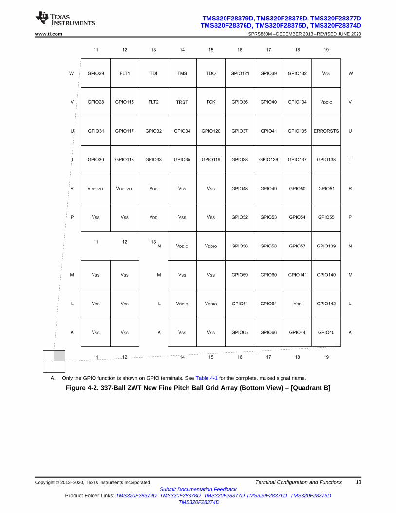
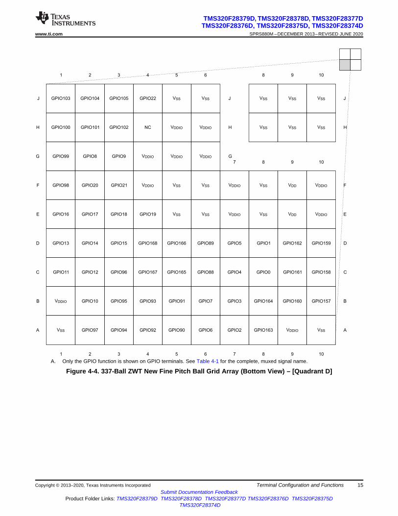
A. Only the GPIO function is shown on GPIO terminals. See Table 4-1 for the complete, muxed signal name.
Figure 4-1. 337-Ball ZWT New Fine Pitch Ball Grid Array (Bottom View) – [Quadrant A]
W
V
U
T
R
P
17161514131211
17161514
VDD
VDD VSS
VSS VSS
VSS
VSS
VSS
VSS
VSS
VSS
VSS
VSS
VSS
VSS
VSS
VSS
VSS
GPIO66GPIO65
GPIO61
GPIO59
GPIO56
GPIO52
GPIO48
GPIO38GPIO119GPIO35GPIO33GPIO118GPIO30
GPIO31
GPIO28
GPIO29
GPIO117
GPIO115
GPIO32 GPIO34 GPIO120
TCKTRST
TDOTDI TMSFLT1
FLT2
GPIO37
GPIO36
GPIO121
GPIO64
GPIO60
GPIO58
GPIO53
GPIO49
GPIO136
GPIO41
GPIO40
GPIO39
VDDIOVDDIO
VDDIOVDDIO
VDD3VFL VDD3VFL
1918
1918
VSS
W
V
U
T
R
P
N
M
L
KGPIO45GPIO44
GPIO142
GPIO140GPIO141
GPIO57 GPIO139
GPIO55GPIO54
GPIO50
GPIO137
GPIO135
GPIO134
GPIO132
GPIO51
GPIO138
ERRORSTS
VDDIO
VSS
1211
M
L
K
N
M
L
K
131211
13
TMS320F28379D, TMS320F28378D, TMS320F28377DTMS320F28376D, TMS320F28375D, TMS320F28374D
www.ti.com SPRS880M –DECEMBER 2013–REVISED JUNE 2020
Submit Documentation FeedbackProduct Folder Links: TMS320F28379D TMS320F28378D TMS320F28377D TMS320F28376D TMS320F28375D
TMS320F28374D
Terminal Configuration and FunctionsCopyright © 2013–2020, Texas Instruments Incorporated
A. Only the GPIO function is shown on GPIO terminals. See Table 4-1 for the complete, muxed signal name.
Figure 4-2. 337-Ball ZWT New Fine Pitch Ball Grid Array (Bottom View) – [Quadrant B]

F
E
D
C
B
A
191817161514
191817161514131211
X1
X2VREGENZ
GPIO67GPIO69
GPIO70GPIO73GPIO77GPIO81GPIO149GPIO153GPIO84
GPIO85
GPIO86
GPIO87
GPIO154
GPIO155
GPIO156
GPIO150
GPIO151
GPIO152
GPIO82
GPIO83
GPIO148
GPIO78
GPIO79
GPIO80
GPIO72
GPIO76
GPIO75
GPIO71
GPIO74
GPIO147
GPIO145
GPIO144
GPIO68
GPIO146
GPIO143
GPIO133
GPIO62GPIO63
GPIO47
GPIO43
GPIO42
GPIO46
XRS
H
G
F
E
D
C
B
A
J
VSS
VSS
VSS
VSS
VSS VSS VSS
VSS
VSS
VSS
VSS
VSS
VSS
VSS
VSSVDD
VDD
VDD
VDD
VDD VDD
VDDIO
VDDOSCVDDOSC
VDDIO
VDDIO
VDDIO
VDDIO
VSSOSC VSSOSCH
J
1211
131211
H
G
J
14
TMS320F28379D, TMS320F28378D, TMS320F28377DTMS320F28376D, TMS320F28375D, TMS320F28374DSPRS880M –DECEMBER 2013–REVISED JUNE 2020 www.ti.com
Submit Documentation FeedbackProduct Folder Links: TMS320F28379D TMS320F28378D TMS320F28377D TMS320F28376D TMS320F28375D
TMS320F28374D
Terminal Configuration and Functions Copyright © 2013–2020, Texas Instruments Incorporated
A. Only the GPIO function is shown on GPIO terminals. See Table 4-1 for the complete, muxed signal name.
Figure 4-3. 337-Ball ZWT New Fine Pitch Ball Grid Array (Bottom View) – [Quadrant C]
J
H
G
F
E
D
C
B
A
654321
7654321
GPIO2GPIO6GPIO90GPIO92GPIO94GPIO97
GPIO10
GPIO11
GPIO13
GPIO16
GPIO98
GPIO99
GPIO100
GPIO103
GPIO12
GPIO14
GPIO17
GPIO20
GPIO95
GPIO96
GPIO15
GPIO18
GPIO21
GPIO9GPIO8
GPIO101
GPIO104
GPIO102
GPIO105
GPIO93
GPIO167
GPIO168
GPIO19
GPIO22
GPIO91
GPIO165
GPIO166
GPIO7
GPIO88
GPIO89
GPIO3
GPIO4
GPIO5
VDDIO
VDDIO
VSS
VSS
VSS VSS
VSS
VSS
VSS
VDDIO
VDDIO
VDDIO
VDDIO
VDDIO
VDDIO
VDDIONC
VSS
VSS VSS VSS
VSS VSS
1098
J
H
J
H
G
1098
F
E
D
C
BGPIO157GPIO160
GPIO163
GPIO164
GPIO0
GPIO1
GPIO161
GPIO162
GPIO158
GPIO159
A
VDD
VDD
VSS
VSS
VSS
VDDIO
VDDIO
VDDIO
10987
15
TMS320F28379D, TMS320F28378D, TMS320F28377DTMS320F28376D, TMS320F28375D, TMS320F28374D
www.ti.com SPRS880M –DECEMBER 2013–REVISED JUNE 2020
Submit Documentation FeedbackProduct Folder Links: TMS320F28379D TMS320F28378D TMS320F28377D TMS320F28376D TMS320F28375D
TMS320F28374D
Terminal Configuration and FunctionsCopyright © 2013–2020, Texas Instruments Incorporated
A. Only the GPIO function is shown on GPIO terminals. See Table 4-1 for the complete, muxed signal name.
Figure 4-4. 337-Ball ZWT New Fine Pitch Ball Grid Array (Bottom View) – [Quadrant D]

88
87
86
85
84
83
82
81
80
79
78
77
76
75
74
73
72
71
70
69
68
67
66
65
64
63
62
61
60
59
58
57
56
55
54
53
52
51
50
49
48
47
46
45
133
134
135
136
137
138
139
140
141
142
143
144
145
146
147
148
149
150
151
152
153
154
155
156
157
158
159
160
161
162
163
164
165
166
167
168
169
170
171
172
173
174
175
176
1 2 3 4 5 6 7 8 9 10
11
12
13
14
15
16
17
18
19
20
21
22
23
24
25
26
27
28
29
30
31
32
33
34
35
36
37
38
39
40
41
42
43
44
132
131
130
129
128
127
126
125
124
123
122
121
120
119
118
117
116
115
114
113
112
111
110
109
108
107
106
105
104
103
102
101
100
99
98
97
96
95
94
93
92
91
90
89
VDD
VDD
VDDA
VREFHIB
VREFLOB
VREFLOD
VREFHID
VSSA
GPIO40
GPIO39
GPIO38
GPIO37
TCK
TMS
TDO
TDI
GPIO35
GPIO34
GPIO33
GPIO32
GPIO31
GPIO29
GPIO28
GPIO30
ADCIND4
ADCIND3
ADCIND2
ADCIND1
ADCIND0
ADCINB3
ADCINB2
ADCINB1
ADCINB0
ADCIN15
FLT1
FLT2
TRST
GPIO36
VDDIO
VDDIO
VDDIO
VDDIO
VDDIO
VDD3VFL
GP
IO67
GP
IO133
GP
IO45
GP
IO44
GP
IO66
GP
IO65
GP
IO64
GP
IO63
GP
IO62
GP
IO61
GP
IO60
GP
IO59
GP
IO58
GP
IO57
GP
IO56
GP
IO55
GP
IO54
GP
IO53
GP
IO52
GP
IO51
GP
IO50
GP
IO49
GP
IO48
GP
IO41
ER
RO
RS
TS
VR
EG
EN
Z
X1
X2
XR
S
GP
IO43
GP
IO42
GP
IO47
GP
IO46
VS
SO
SC
VD
D
VD
D
VD
DIO
VD
DO
SC
VD
DO
SC
VD
DIO
VD
DIO
VD
DIO
VD
DIO
VD
DIO
GP
IO10
GP
IO11
GP
IO12
GP
IO13
GP
IO14
GP
IO15
GP
IO16
GP
IO17
GP
IO18
GP
IO19
GP
IO20
GP
IO8
GP
IO9
GP
IO22
GP
IO23
GP
IO24
GP
IO25
GP
IO26
GP
IO27
AD
CIN
C4
AD
CIN
C3
AD
CIN
C2
AD
CIN
A5
AD
CIN
A4
AD
CIN
A3
AD
CIN
A2
AD
CIN
A1
AD
CIN
A0
AD
CIN
14
GP
IO21
VS
SA
VD
DA
VR
EF
HIC
VR
EF
LO
C
VR
EF
LO
A
VR
EF
HIA
VD
D
GP
IO99
VD
D
VD
DIO
VD
DIO
VD
DIO
VD
DIO
VD
DIO
GPIO68
GPIO69
GPIO70
GPIO71
GPIO72
GPIO73
GPIO74
GPIO75
GPIO76
GPIO77
GPIO78
GPIO79
GPIO80
GPIO81
GPIO82
GPIO83
GPIO0
GPIO1
GPIO2
GPIO3
GPIO4
GPIO5
GPIO6
GPIO7
GPIO88
GPIO89
GPIO90
GPIO91
GPIO92
GPIO93
GPIO94
GPIO84
GPIO85
GPIO86
GPIO87
VDD
VDD
VDD
VDDIO
VDDIO
VDDIO
VDDIO
VDDIO
VDD
16
TMS320F28379D, TMS320F28378D, TMS320F28377DTMS320F28376D, TMS320F28375D, TMS320F28374DSPRS880M –DECEMBER 2013–REVISED JUNE 2020 www.ti.com
Submit Documentation FeedbackProduct Folder Links: TMS320F28379D TMS320F28378D TMS320F28377D TMS320F28376D TMS320F28375D
TMS320F28374D
Terminal Configuration and Functions Copyright © 2013–2020, Texas Instruments Incorporated
A. Only the GPIO function is shown on GPIO pins. See Table 4-1 for the complete, muxed signal name.
Figure 4-5. 176-Pin PTP PowerPAD Thermally Enhanced Low-Profile Quad Flatpack (Top View)
75
74
73
72
71
70
69
68
67
66
65
64
63
62
50
49
48
47
46
45
44
43
42
41
40
39
38
37
76
77
78
79
80
81
82
83
84
85
86
87
88
89
1 2 3 4 5 6 7 8 9 10
11
12
13
14
61
60
59
58
57
56
15
16
17
18
19
20
90
91
92
93
94
95
36
35
34
33
32
31
21
22
23
24
25
30
29
28
27
26
55
54
53
52
51
96
97
98
99
100
GPIO70
GPIO71
GPIO72
GPIO73
GPIO78
GPIO84
GPIO85
GPIO86
GPIO87
GPIO2
GPIO3
GPIO4
GPIO89
GPIO90
GPIO91
GPIO92
GPIO10
VDD
VDD
VDD
VDDIO
VDDIO
VDDIO
VDDIO
VDD
GP
IO11
AD
CIN
A3
AD
CIN
A0
AD
CIN
A1
AD
CIN
A2
AD
CIN
A4
AD
CIN
A5
GP
IO21
GP
IO20
GP
IO99
GP
IO18
GP
IO19
GP
IO17
GP
IO16
GP
IO15
GP
IO14
GP
IO13
GP
IO12
TCK
TDO
TDI
FLT1
FLT2
ADCINB5
ADCINB4
ADCINB3
ADCINB2
ADCINB1
ADCINB0
ADCIN15
ADCIN14
VDD
VDD
VSSA
VDD3VFL
VDDIO
VDDA
VREFHIB
VSSA
VREFLOB
VDDIO
TMS
TRST
GP
IO69
GP
IO41
GP
IO58
GP
IO59
GP
IO60
GP
IO61
GP
IO62
GP
IO63
GP
IO64
GP
IO65
GP
IO66
VR
EG
EN
Z
X1
X2
GP
IO43
GP
IO42
XR
S
VD
DIO
VD
DO
SC
VD
DIO
VD
DIO
VD
DO
SC
VD
D
VD
D
VS
SO
SC
VD
DIO
VD
DIO
VD
DIO
VD
D
V/V
SS
AR
EF
LO
A
VD
DA
VR
EF
HIA
17
TMS320F28379D, TMS320F28378D, TMS320F28377DTMS320F28376D, TMS320F28375D, TMS320F28374D
www.ti.com SPRS880M –DECEMBER 2013–REVISED JUNE 2020
Submit Documentation FeedbackProduct Folder Links: TMS320F28379D TMS320F28378D TMS320F28377D TMS320F28376D TMS320F28375D
TMS320F28374D
Terminal Configuration and FunctionsCopyright © 2013–2020, Texas Instruments Incorporated
A. Only the GPIO function is shown on GPIO pins. See Table 4-1 for the complete, muxed signal name.
Figure 4-6. 100-Pin PZP PowerPAD HTQFP (Top View)
NOTEThe exposed lead frame die pad of the PowerPAD™ package serves two functions: toremove heat from the die and to provide ground path for the digital ground (analog ground isprovided through dedicated pins). Thus, the PowerPAD should be soldered to the ground(GND) plane of the PCB because this will provide both the digital ground path and goodthermal conduction path. To make optimum use of the thermal efficiencies designed into thePowerPAD package, the PCB must be designed with this technology in mind. A thermal landis required on the surface of the PCB directly underneath the body of the PowerPAD. Thethermal land should be soldered to the exposed lead frame die pad of the PowerPADpackage; the thermal land should be as large as needed to dissipate the required heat. Anarray of thermal vias should be used to connect the thermal pad to the internal GND plane ofthe board. See PowerPAD™ Thermally Enhanced Package for more details on using thePowerPAD package.

18
TMS320F28379D, TMS320F28378D, TMS320F28377DTMS320F28376D, TMS320F28375D, TMS320F28374DSPRS880M –DECEMBER 2013–REVISED JUNE 2020 www.ti.com
Submit Documentation FeedbackProduct Folder Links: TMS320F28379D TMS320F28378D TMS320F28377D TMS320F28376D TMS320F28375D
TMS320F28374D
Terminal Configuration and Functions Copyright © 2013–2020, Texas Instruments Incorporated
NOTEPCB footprints and schematic symbols are available for download in a vendor-neutral format,which can be exported to the leading EDA CAD/CAE design tools. See the CAD/CAESymbols section in the product folder for each device, under the Packaging section. Thesefootprints and symbols can also be searched for at http://webench.ti.com/cad/.
19
TMS320F28379D, TMS320F28378D, TMS320F28377DTMS320F28376D, TMS320F28375D, TMS320F28374D
www.ti.com SPRS880M –DECEMBER 2013–REVISED JUNE 2020
Submit Documentation FeedbackProduct Folder Links: TMS320F28379D TMS320F28378D TMS320F28377D TMS320F28376D TMS320F28375D
TMS320F28374D
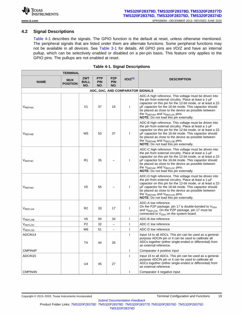
Terminal Configuration and FunctionsCopyright © 2013–2020, Texas Instruments Incorporated
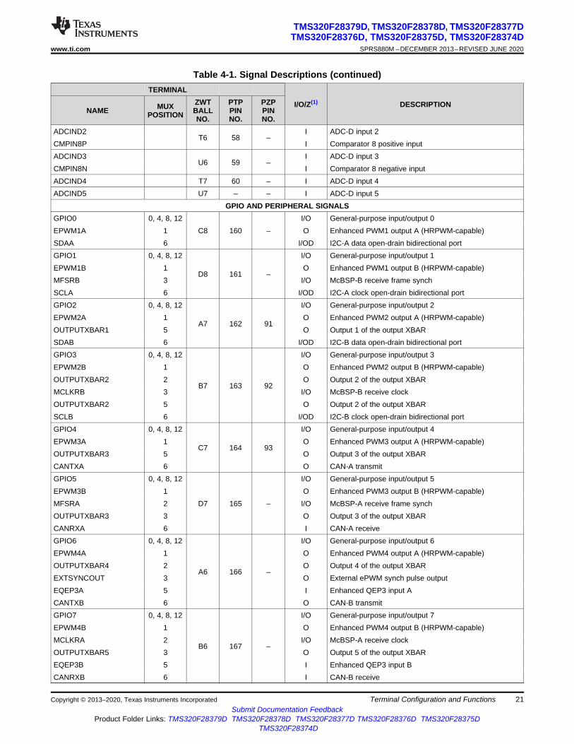
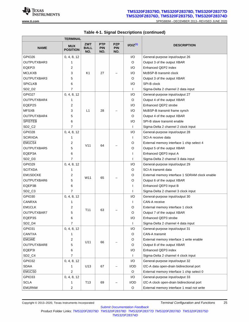
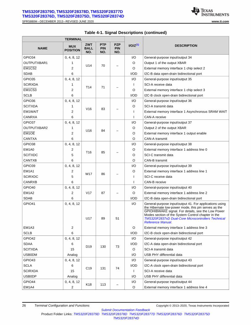
4.2 Signal DescriptionsTable 4-1 describes the signals. The GPIO function is the default at reset, unless otherwise mentioned.The peripheral signals that are listed under them are alternate functions. Some peripheral functions maynot be available in all devices. See Table 3-1 for details. All GPIO pins are I/O/Z and have an internalpullup, which can be selectively enabled or disabled on a per-pin basis. This feature only applies to theGPIO pins. The pullups are not enabled at reset.
Table 4-1. Signal DescriptionsTERMINAL
I/O/Z(1) DESCRIPTIONNAME MUX
POSITIONZWTBALLNO.
PTPPINNO.
PZPPINNO.
ADC, DAC, AND COMPARATOR SIGNALS
VREFHIA V1 37 19 I
ADC-A high reference. This voltage must be driven intothe pin from external circuitry. Place at least a 1-µFcapacitor on this pin for the 12-bit mode, or at least a 22-µF capacitor for the 16-bit mode. This capacitor shouldbe placed as close to the device as possible betweenthe VREFHIA and VREFLOA pins.NOTE: Do not load this pin externally.
VREFHIB W5 53 37 I
ADC-B high reference. This voltage must be driven intothe pin from external circuitry. Place at least a 1-µFcapacitor on this pin for the 12-bit mode, or at least a 22-µF capacitor for the 16-bit mode. This capacitor shouldbe placed as close to the device as possible betweenthe VREFHIB and VREFLOB pins.NOTE: Do not load this pin externally.
VREFHIC R1 35 – I
ADC-C high reference. This voltage must be driven intothe pin from external circuitry. Place at least a 1-µFcapacitor on this pin for the 12-bit mode, or at least a 22-µF capacitor for the 16-bit mode. This capacitor shouldbe placed as close to the device as possible betweenthe VREFHIC and VREFLOC pins.NOTE: Do not load this pin externally.
VREFHID V5 55 – I
ADC-D high reference. This voltage must be driven intothe pin from external circuitry. Place at least a 1-µFcapacitor on this pin for the 12-bit mode, or at least a 22-µF capacitor for the 16-bit mode. This capacitor shouldbe placed as close to the device as possible betweenthe VREFHID and VREFLOD pins.NOTE: Do not load this pin externally.
VREFLOA R2 33 17 I
ADC-A low reference.On the PZP package, pin 17 is double-bonded to VSSAand VREFLOA. On the PZP package, pin 17 must beconnected to VSSA on the system board.
VREFLOB V6 50 34 I ADC-B low referenceVREFLOC P2 32 – I ADC-C low referenceVREFLOD W6 51 – I ADC-D low referenceADCIN14
T4 44 26
I Input 14 to all ADCs. This pin can be used as a general-purpose ADCIN pin or it can be used to calibrate allADCs together (either single-ended or differential) froman external reference.
CMPIN4P I Comparator 4 positive inputADCIN15
U4 45 27
I Input 15 to all ADCs. This pin can be used as a general-purpose ADCIN pin or it can be used to calibrate allADCs together (either single-ended or differential) froman external reference.
CMPIN4N I Comparator 4 negative input

20
TMS320F28379D, TMS320F28378D, TMS320F28377DTMS320F28376D, TMS320F28375D, TMS320F28374DSPRS880M –DECEMBER 2013–REVISED JUNE 2020 www.ti.com
Submit Documentation FeedbackProduct Folder Links: TMS320F28379D TMS320F28378D TMS320F28377D TMS320F28376D TMS320F28375D
TMS320F28374D
Terminal Configuration and Functions Copyright © 2013–2020, Texas Instruments Incorporated
Table 4-1. Signal Descriptions (continued)TERMINAL
I/O/Z(1) DESCRIPTIONNAME MUX
POSITIONZWTBALLNO.
PTPPINNO.
PZPPINNO.
ADCINA0
U1 43 25
I ADC-A input 0. There is a 50-kΩ internal pulldown onthis pin in both an ADC input or DAC output mode whichcannot be disabled.
DACOUTA O DAC-A outputADCINA1
T1 42 24
I ADC-A input 1. There is a 50-kΩ internal pulldown onthis pin in both an ADC input or DAC output mode whichcannot be disabled.
DACOUTB O DAC-B outputADCINA2
U2 41 23I ADC-A input 2
CMPIN1P I Comparator 1 positive inputADCINA3
T2 40 22I ADC-A input 3
CMPIN1N I Comparator 1 negative inputADCINA4
U3 39 21I ADC-A input 4
CMPIN2P I Comparator 2 positive inputADCINA5
T3 38 20I ADC-A input 5
CMPIN2N I Comparator 2 negative inputADCINB0
V2 46 28
I ADC-B input 0. There is a 100-pF capacitor to VSSA onthis pin in both ADC input or DAC reference mode whichcannot be disabled. If this pin is being used as areference for the on-chip DACs, place at least a 1-µFcapacitor on this pin.
VDAC I Optional external reference voltage for on-chip DACs.There is a 100-pF capacitor to VSSA on this pin in bothADC input or DAC reference mode which cannot bedisabled. If this pin is being used as a reference for theon-chip DACs, place at least a 1-µF capacitor on thispin.
ADCINB1
W2 47 29
I ADC-B input 1. There is a 50-kΩ internal pulldown onthis pin in both an ADC input or DAC output mode whichcannot be disabled.
DACOUTC O DAC-C outputADCINB2
V3 48 30I ADC-B input 2
CMPIN3P I Comparator 3 positive inputADCINB3
W3 49 31I ADC-B input 3
CMPIN3N I Comparator 3 negative inputADCINB4 V4 – 32 I ADC-B input 4ADCINB5 W4 – 33 I ADC-B input 5ADCINC2
R3 31 –I ADC-C input 2
CMPIN6P I Comparator 6 positive inputADCINC3
P3 30 –I ADC-C input 3
CMPIN6N I Comparator 6 negative inputADCINC4
R4 29 –I ADC-C input 4
CMPIN5P I Comparator 5 positive inputADCINC5
P4 – –I ADC-C input 5
CMPIN5N I Comparator 5 negative inputADCIND0
T5 56 –I ADC-D input 0
CMPIN7P I Comparator 7 positive inputADCIND1
U5 57 –I ADC-D input 1
CMPIN7N I Comparator 7 negative input
21
TMS320F28379D, TMS320F28378D, TMS320F28377DTMS320F28376D, TMS320F28375D, TMS320F28374D
www.ti.com SPRS880M –DECEMBER 2013–REVISED JUNE 2020
Submit Documentation FeedbackProduct Folder Links: TMS320F28379D TMS320F28378D TMS320F28377D TMS320F28376D TMS320F28375D
TMS320F28374D
Terminal Configuration and FunctionsCopyright © 2013–2020, Texas Instruments Incorporated
Table 4-1. Signal Descriptions (continued)TERMINAL
I/O/Z(1) DESCRIPTIONNAME MUX
POSITIONZWTBALLNO.
PTPPINNO.
PZPPINNO.
ADCIND2T6 58 –
I ADC-D input 2CMPIN8P I Comparator 8 positive inputADCIND3
U6 59 –I ADC-D input 3
CMPIN8N I Comparator 8 negative inputADCIND4 T7 60 – I ADC-D input 4ADCIND5 U7 – – I ADC-D input 5
GPIO AND PERIPHERAL SIGNALSGPIO0 0, 4, 8, 12
C8 160 –I/O General-purpose input/output 0
EPWM1A 1 O Enhanced PWM1 output A (HRPWM-capable)SDAA 6 I/OD I2C-A data open-drain bidirectional portGPIO1 0, 4, 8, 12
D8 161 –
I/O General-purpose input/output 1EPWM1B 1 O Enhanced PWM1 output B (HRPWM-capable)MFSRB 3 I/O McBSP-B receive frame synchSCLA 6 I/OD I2C-A clock open-drain bidirectional portGPIO2 0, 4, 8, 12
A7 162 91
I/O General-purpose input/output 2EPWM2A 1 O Enhanced PWM2 output A (HRPWM-capable)OUTPUTXBAR1 5 O Output 1 of the output XBARSDAB 6 I/OD I2C-B data open-drain bidirectional portGPIO3 0, 4, 8, 12
B7 163 92
I/O General-purpose input/output 3EPWM2B 1 O Enhanced PWM2 output B (HRPWM-capable)OUTPUTXBAR2 2 O Output 2 of the output XBARMCLKRB 3 I/O McBSP-B receive clockOUTPUTXBAR2 5 O Output 2 of the output XBARSCLB 6 I/OD I2C-B clock open-drain bidirectional portGPIO4 0, 4, 8, 12
C7 164 93
I/O General-purpose input/output 4EPWM3A 1 O Enhanced PWM3 output A (HRPWM-capable)OUTPUTXBAR3 5 O Output 3 of the output XBARCANTXA 6 O CAN-A transmitGPIO5 0, 4, 8, 12
D7 165 –
I/O General-purpose input/output 5EPWM3B 1 O Enhanced PWM3 output B (HRPWM-capable)MFSRA 2 I/O McBSP-A receive frame synchOUTPUTXBAR3 3 O Output 3 of the output XBARCANRXA 6 I CAN-A receiveGPIO6 0, 4, 8, 12
A6 166 –
I/O General-purpose input/output 6EPWM4A 1 O Enhanced PWM4 output A (HRPWM-capable)OUTPUTXBAR4 2 O Output 4 of the output XBAREXTSYNCOUT 3 O External ePWM synch pulse outputEQEP3A 5 I Enhanced QEP3 input ACANTXB 6 O CAN-B transmitGPIO7 0, 4, 8, 12
B6 167 –
I/O General-purpose input/output 7EPWM4B 1 O Enhanced PWM4 output B (HRPWM-capable)MCLKRA 2 I/O McBSP-A receive clockOUTPUTXBAR5 3 O Output 5 of the output XBAREQEP3B 5 I Enhanced QEP3 input BCANRXB 6 I CAN-B receive

22
TMS320F28379D, TMS320F28378D, TMS320F28377DTMS320F28376D, TMS320F28375D, TMS320F28374DSPRS880M –DECEMBER 2013–REVISED JUNE 2020 www.ti.com
Submit Documentation FeedbackProduct Folder Links: TMS320F28379D TMS320F28378D TMS320F28377D TMS320F28376D TMS320F28375D
TMS320F28374D
Terminal Configuration and Functions Copyright © 2013–2020, Texas Instruments Incorporated
Table 4-1. Signal Descriptions (continued)TERMINAL
I/O/Z(1) DESCRIPTIONNAME MUX
POSITIONZWTBALLNO.
PTPPINNO.
PZPPINNO.
GPIO8 0, 4, 8, 12
G2 18 –
I/O General-purpose input/output 8EPWM5A 1 O Enhanced PWM5 output A (HRPWM-capable)CANTXB 2 O CAN-B transmitADCSOCAO 3 O ADC start-of-conversion A output for external ADCEQEP3S 5 I/O Enhanced QEP3 strobeSCITXDA 6 O SCI-A transmit dataGPIO9 0, 4, 8, 12
G3 19 –
I/O General-purpose input/output 9EPWM5B 1 O Enhanced PWM5 output B (HRPWM-capable)SCITXDB 2 O SCI-B transmit dataOUTPUTXBAR6 3 O Output 6 of the output XBAREQEP3I 5 I/O Enhanced QEP3 indexSCIRXDA 6 I SCI-A receive dataGPIO10 0, 4, 8, 12
B2 1 100
I/O General-purpose input/output 10EPWM6A 1 O Enhanced PWM6 output A (HRPWM-capable)CANRXB 2 I CAN-B receiveADCSOCBO 3 O ADC start-of-conversion B output for external ADCEQEP1A 5 I Enhanced QEP1 input ASCITXDB 6 O SCI-B transmit dataUPP-WAIT 15 I/O Universal parallel port wait. Receiver asserts to request
a pause in transfer.GPIO11 0, 4, 8, 12
C1 2 1
I/O General-purpose input/output 11EPWM6B 1 O Enhanced PWM6 output B (HRPWM-capable)SCIRXDB 2, 6 I SCI-B receive dataOUTPUTXBAR7 3 O Output 7 of the output XBAREQEP1B 5 I Enhanced QEP1 input BUPP-START 15 I/O Universal parallel port start. Transmitter asserts at start
of DMA line.GPIO12 0, 4, 8, 12
C2 4 3
I/O General-purpose input/output 12EPWM7A 1 O Enhanced PWM7 output A (HRPWM-capable)CANTXB 2 O CAN-B transmitMDXB 3 O McBSP-B transmit serial dataEQEP1S 5 I/O Enhanced QEP1 strobeSCITXDC 6 O SCI-C transmit dataUPP-ENA 15 I/O Universal parallel port enable. Transmitter asserts while
data bus is active.GPIO13 0, 4, 8, 12
D1 5 4
I/O General-purpose input/output 13EPWM7B 1 O Enhanced PWM7 output B (HRPWM-capable)CANRXB 2 I CAN-B receiveMDRB 3 I McBSP-B receive serial dataEQEP1I 5 I/O Enhanced QEP1 indexSCIRXDC 6 I SCI-C receive dataUPP-D7 15 I/O Universal parallel port data line 7

23
TMS320F28379D, TMS320F28378D, TMS320F28377DTMS320F28376D, TMS320F28375D, TMS320F28374D
www.ti.com SPRS880M –DECEMBER 2013–REVISED JUNE 2020
Submit Documentation FeedbackProduct Folder Links: TMS320F28379D TMS320F28378D TMS320F28377D TMS320F28376D TMS320F28375D
TMS320F28374D
Terminal Configuration and FunctionsCopyright © 2013–2020, Texas Instruments Incorporated
Table 4-1. Signal Descriptions (continued)TERMINAL
I/O/Z(1) DESCRIPTIONNAME MUX
POSITIONZWTBALLNO.
PTPPINNO.
PZPPINNO.
GPIO14 0, 4, 8, 12
D2 6 5
I/O General-purpose input/output 14EPWM8A 1 O Enhanced PWM8 output A (HRPWM-capable)SCITXDB 2 O SCI-B transmit dataMCLKXB 3 I/O McBSP-B transmit clockOUTPUTXBAR3 6 O Output 3 of the output XBARUPP-D6 15 I/O Universal parallel port data line 6GPIO15 0, 4, 8, 12
D3 7 6
I/O General-purpose input/output 15EPWM8B 1 O Enhanced PWM8 output B (HRPWM-capable)SCIRXDB 2 I SCI-B receive dataMFSXB 3 I/O McBSP-B transmit frame synchOUTPUTXBAR4 6 O Output 4 of the output XBARUPP-D5 15 I/O Universal parallel port data line 5GPIO16 0, 4, 8, 12
E1 8 7
I/O General-purpose input/output 16SPISIMOA 1 I/O SPI-A slave in, master outCANTXB 2 O CAN-B transmitOUTPUTXBAR7 3 O Output 7 of the output XBAREPWM9A 5 O Enhanced PWM9 output ASD1_D1 7 I Sigma-Delta 1 channel 1 data inputUPP-D4 15 I/O Universal parallel port data line 4GPIO17 0, 4, 8, 12
E2 9 8
I/O General-purpose input/output 17SPISOMIA 1 I/O SPI-A slave out, master inCANRXB 2 I CAN-B receiveOUTPUTXBAR8 3 O Output 8 of the output XBAREPWM9B 5 O Enhanced PWM9 output BSD1_C1 7 I Sigma-Delta 1 channel 1 clock inputUPP-D3 15 I/O Universal parallel port data line 3GPIO18 0, 4, 8, 12
E3 10 9
I/O General-purpose input/output 18SPICLKA 1 I/O SPI-A clockSCITXDB 2 O SCI-B transmit dataCANRXA 3 I CAN-A receiveEPWM10A 5 O Enhanced PWM10 output ASD1_D2 7 I Sigma-Delta 1 channel 2 data inputUPP-D2 15 I/O Universal parallel port data line 2GPIO19 0, 4, 8, 12
E4 12 11
I/O General-purpose input/output 19SPISTEA 1 I/O SPI-A slave transmit enableSCIRXDB 2 I SCI-B receive dataCANTXA 3 O CAN-A transmitEPWM10B 5 O Enhanced PWM10 output BSD1_C2 7 I Sigma-Delta 1 channel 2 clock inputUPP-D1 15 I/O Universal parallel port data line 1

24
TMS320F28379D, TMS320F28378D, TMS320F28377DTMS320F28376D, TMS320F28375D, TMS320F28374DSPRS880M –DECEMBER 2013–REVISED JUNE 2020 www.ti.com
Submit Documentation FeedbackProduct Folder Links: TMS320F28379D TMS320F28378D TMS320F28377D TMS320F28376D TMS320F28375D
TMS320F28374D
Terminal Configuration and Functions Copyright © 2013–2020, Texas Instruments Incorporated
Table 4-1. Signal Descriptions (continued)TERMINAL
I/O/Z(1) DESCRIPTIONNAME MUX
POSITIONZWTBALLNO.
PTPPINNO.
PZPPINNO.
GPIO20 0, 4, 8, 12
F2 13 12
I/O General-purpose input/output 20EQEP1A 1 I Enhanced QEP1 input AMDXA 2 O McBSP-A transmit serial dataCANTXB 3 O CAN-B transmitEPWM11A 5 O Enhanced PWM11 output ASD1_D3 7 I Sigma-Delta 1 channel 3 data inputUPP-D0 15 I/O Universal parallel port data line 0GPIO21 0, 4, 8, 12
F3 14 13
I/O General-purpose input/output 21EQEP1B 1 I Enhanced QEP1 input BMDRA 2 I McBSP-A receive serial dataCANRXB 3 I CAN-B receiveEPWM11B 5 O Enhanced PWM11 output BSD1_C3 7 I Sigma-Delta 1 channel 3 clock inputUPP-CLK 15 I/O Universal parallel port transmit clockGPIO22 0, 4, 8, 12
J4 22 –
I/O General-purpose input/output 22EQEP1S 1 I/O Enhanced QEP1 strobeMCLKXA 2 I/O McBSP-A transmit clockSCITXDB 3 O SCI-B transmit dataEPWM12A 5 O Enhanced PWM12 output ASPICLKB 6 I/O SPI-B clockSD1_D4 7 I Sigma-Delta 1 channel 4 data inputGPIO23 0, 4, 8, 12
K4 23 –
I/O General-purpose input/output 23EQEP1I 1 I/O Enhanced QEP1 indexMFSXA 2 I/O McBSP-A transmit frame synchSCIRXDB 3 I SCI-B receive dataEPWM12B 5 O Enhanced PWM12 output BSPISTEB 6 I/O SPI-B slave transmit enableSD1_C4 7 I Sigma-Delta 1 channel 4 clock inputGPIO24 0, 4, 8, 12
K3 24 –
I/O General-purpose input/output 24OUTPUTXBAR1 1 O Output 1 of the output XBAREQEP2A 2 I Enhanced QEP2 input AMDXB 3 O McBSP-B transmit serial dataSPISIMOB 6 I/O SPI-B slave in, master outSD2_D1 7 I Sigma-Delta 2 channel 1 data inputGPIO25 0, 4, 8, 12
K2 25 –
I/O General-purpose input/output 25OUTPUTXBAR2 1 O Output 2 of the output XBAREQEP2B 2 I Enhanced QEP2 input BMDRB 3 I McBSP-B receive serial dataSPISOMIB 6 I/O SPI-B slave out, master inSD2_C1 7 I Sigma-Delta 2 channel 1 clock input
25
TMS320F28379D, TMS320F28378D, TMS320F28377DTMS320F28376D, TMS320F28375D, TMS320F28374D
www.ti.com SPRS880M –DECEMBER 2013–REVISED JUNE 2020
Submit Documentation FeedbackProduct Folder Links: TMS320F28379D TMS320F28378D TMS320F28377D TMS320F28376D TMS320F28375D
TMS320F28374D
Terminal Configuration and FunctionsCopyright © 2013–2020, Texas Instruments Incorporated
Table 4-1. Signal Descriptions (continued)TERMINAL
I/O/Z(1) DESCRIPTIONNAME MUX
POSITIONZWTBALLNO.
PTPPINNO.
PZPPINNO.
GPIO26 0, 4, 8, 12
K1 27 –
I/O General-purpose input/output 26OUTPUTXBAR3 1 O Output 3 of the output XBAREQEP2I 2 I/O Enhanced QEP2 indexMCLKXB 3 I/O McBSP-B transmit clockOUTPUTXBAR3 5 O Output 3 of the output XBARSPICLKB 6 I/O SPI-B clockSD2_D2 7 I Sigma-Delta 2 channel 2 data inputGPIO27 0, 4, 8, 12
L1 28 –
I/O General-purpose input/output 27OUTPUTXBAR4 1 O Output 4 of the output XBAREQEP2S 2 I/O Enhanced QEP2 strobeMFSXB 3 I/O McBSP-B transmit frame synchOUTPUTXBAR4 5 O Output 4 of the output XBARSPISTEB 6 I/O SPI-B slave transmit enableSD2_C2 7 I Sigma-Delta 2 channel 2 clock inputGPIO28 0, 4, 8, 12
V11 64 –
I/O General-purpose input/output 28SCIRXDA 1 I SCI-A receive dataEM1CS4 2 O External memory interface 1 chip select 4OUTPUTXBAR5 5 O Output 5 of the output XBAREQEP3A 6 I Enhanced QEP3 input ASD2_D3 7 I Sigma-Delta 2 channel 3 data inputGPIO29 0, 4, 8, 12
W11 65 –
I/O General-purpose input/output 29SCITXDA 1 O SCI-A transmit dataEM1SDCKE 2 O External memory interface 1 SDRAM clock enableOUTPUTXBAR6 5 O Output 6 of the output XBAREQEP3B 6 I Enhanced QEP3 input BSD2_C3 7 I Sigma-Delta 2 channel 3 clock inputGPIO30 0, 4, 8, 12
T11 63 –
I/O General-purpose input/output 30CANRXA 1 I CAN-A receiveEM1CLK 2 O External memory interface 1 clockOUTPUTXBAR7 5 O Output 7 of the output XBAREQEP3S 6 I/O Enhanced QEP3 strobeSD2_D4 7 I Sigma-Delta 2 channel 4 data inputGPIO31 0, 4, 8, 12
U11 66 –
I/O General-purpose input/output 31CANTXA 1 O CAN-A transmitEM1WE 2 O External memory interface 1 write enableOUTPUTXBAR8 5 O Output 8 of the output XBAREQEP3I 6 I/O Enhanced QEP3 indexSD2_C4 7 I Sigma-Delta 2 channel 4 clock inputGPIO32 0, 4, 8, 12
U13 67 –I/O General-purpose input/output 32
SDAA 1 I/OD I2C-A data open-drain bidirectional portEM1CS0 2 O External memory interface 1 chip select 0GPIO33 0, 4, 8, 12
T13 69 –I/O General-purpose input/output 33
SCLA 1 I/OD I2C-A clock open-drain bidirectional portEM1RNW 2 O External memory interface 1 read not write
26
TMS320F28379D, TMS320F28378D, TMS320F28377DTMS320F28376D, TMS320F28375D, TMS320F28374DSPRS880M –DECEMBER 2013–REVISED JUNE 2020 www.ti.com
Submit Documentation FeedbackProduct Folder Links: TMS320F28379D TMS320F28378D TMS320F28377D TMS320F28376D TMS320F28375D
TMS320F28374D
Terminal Configuration and Functions Copyright © 2013–2020, Texas Instruments Incorporated
Table 4-1. Signal Descriptions (continued)TERMINAL
I/O/Z(1) DESCRIPTIONNAME MUX
POSITIONZWTBALLNO.
PTPPINNO.
PZPPINNO.
GPIO34 0, 4, 8, 12
U14 70 –
I/O General-purpose input/output 34OUTPUTXBAR1 1 O Output 1 of the output XBAREM1CS2 2 O External memory interface 1 chip select 2SDAB 6 I/OD I2C-B data open-drain bidirectional portGPIO35 0, 4, 8, 12
T14 71 –
I/O General-purpose input/output 35SCIRXDA 1 I SCI-A receive dataEM1CS3 2 O External memory interface 1 chip select 3SCLB 6 I/OD I2C-B clock open-drain bidirectional portGPIO36 0, 4, 8, 12
V16 83 –
I/O General-purpose input/output 36SCITXDA 1 O SCI-A transmit dataEM1WAIT 2 I External memory interface 1 Asynchronous SRAM WAITCANRXA 6 I CAN-A receiveGPIO37 0, 4, 8, 12
U16 84 –
I/O General-purpose input/output 37OUTPUTXBAR2 1 O Output 2 of the output XBAREM1OE 2 O External memory interface 1 output enableCANTXA 6 O CAN-A transmitGPIO38 0, 4, 8, 12
T16 85 –
I/O General-purpose input/output 38EM1A0 2 O External memory interface 1 address line 0SCITXDC 5 O SCI-C transmit dataCANTXB 6 O CAN-B transmitGPIO39 0, 4, 8, 12
W17 86 –
I/O General-purpose input/output 39EM1A1 2 O External memory interface 1 address line 1SCIRXDC 5 I SCI-C receive dataCANRXB 6 I CAN-B receiveGPIO40 0, 4, 8, 12
V17 87 –I/O General-purpose input/output 40
EM1A2 2 O External memory interface 1 address line 2SDAB 6 I/OD I2C-B data open-drain bidirectional portGPIO41 0, 4, 8, 12
U17 89 51
I/O General-purpose input/output 41. For applications usingthe Hibernate low-power mode, this pin serves as theGPIOHIBWAKE signal. For details, see the Low PowerModes section of the System Control chapter in theTMS320F2837xD Dual-Core Microcontrollers TechnicalReference Manual.
EM1A3 2 O External memory interface 1 address line 3SCLB 6 I/OD I2C-B clock open-drain bidirectional portGPIO42 0, 4, 8, 12
D19 130 73
I/O General-purpose input/output 42SDAA 6 I/OD I2C-A data open-drain bidirectional portSCITXDA 15 O SCI-A transmit dataUSB0DM Analog I/O USB PHY differential dataGPIO43 0, 4, 8, 12
C19 131 74
I/O General-purpose input/output 43SCLA 6 I/OD I2C-A clock open-drain bidirectional portSCIRXDA 15 I SCI-A receive dataUSB0DP Analog I/O USB PHY differential dataGPIO44 0, 4, 8, 12
K18 113 –I/O General-purpose input/output 44
EM1A4 2 O External memory interface 1 address line 4

27
TMS320F28379D, TMS320F28378D, TMS320F28377DTMS320F28376D, TMS320F28375D, TMS320F28374D
www.ti.com SPRS880M –DECEMBER 2013–REVISED JUNE 2020
Submit Documentation FeedbackProduct Folder Links: TMS320F28379D TMS320F28378D TMS320F28377D TMS320F28376D TMS320F28375D
TMS320F28374D
Terminal Configuration and FunctionsCopyright © 2013–2020, Texas Instruments Incorporated
Table 4-1. Signal Descriptions (continued)TERMINAL
I/O/Z(1) DESCRIPTIONNAME MUX
POSITIONZWTBALLNO.
PTPPINNO.
PZPPINNO.
GPIO45 0, 4, 8, 12K19 115 –
I/O General-purpose input/output 45EM1A5 2 O External memory interface 1 address line 5GPIO46 0, 4, 8, 12
E19 128 –I/O General-purpose input/output 46
EM1A6 2 O External memory interface 1 address line 6SCIRXDD 6 I SCI-D receive dataGPIO47 0, 4, 8, 12
E18 129 –I/O General-purpose input/output 47
EM1A7 2 O External memory interface 1 address line 7SCITXDD 6 O SCI-D transmit dataGPIO48 0, 4, 8, 12
R16 90 –
I/O General-purpose input/output 48OUTPUTXBAR3 1 O Output 3 of the output XBAREM1A8 2 O External memory interface 1 address line 8SCITXDA 6 O SCI-A transmit dataSD1_D1 7 I Sigma-Delta 1 channel 1 data inputGPIO49 0, 4, 8, 12
R17 93 –
I/O General-purpose input/output 49OUTPUTXBAR4 1 O Output 4 of the output XBAREM1A9 2 O External memory interface 1 address line 9SCIRXDA 6 I SCI-A receive dataSD1_C1 7 I Sigma-Delta 1 channel 1 clock inputGPIO50 0, 4, 8, 12
R18 94 –
I/O General-purpose input/output 50EQEP1A 1 I Enhanced QEP1 input AEM1A10 2 O External memory interface 1 address line 10SPISIMOC 6 I/O SPI-C slave in, master outSD1_D2 7 I Sigma-Delta 1 channel 2 data inputGPIO51 0, 4, 8, 12
R19 95 –
I/O General-purpose input/output 51EQEP1B 1 I Enhanced QEP1 input BEM1A11 2 O External memory interface 1 address line 11SPISOMIC 6 I/O SPI-C slave out, master inSD1_C2 7 I Sigma-Delta 1 channel 2 clock inputGPIO52 0, 4, 8, 12
P16 96 –
I/O General-purpose input/output 52EQEP1S 1 I/O Enhanced QEP1 strobeEM1A12 2 O External memory interface 1 address line 12SPICLKC 6 I/O SPI-C clockSD1_D3 7 I Sigma-Delta 1 channel 3 data inputGPIO53 0, 4, 8, 12
P17 97 –
I/O General-purpose input/output 53EQEP1I 1 I/O Enhanced QEP1 indexEM1D31 2 I/O External memory interface 1 data line 31EM2D15 3 I/O External memory interface 2 data line 15SPISTEC 6 I/O SPI-C slave transmit enableSD1_C3 7 I Sigma-Delta 1 channel 3 clock input

28
TMS320F28379D, TMS320F28378D, TMS320F28377DTMS320F28376D, TMS320F28375D, TMS320F28374DSPRS880M –DECEMBER 2013–REVISED JUNE 2020 www.ti.com
Submit Documentation FeedbackProduct Folder Links: TMS320F28379D TMS320F28378D TMS320F28377D TMS320F28376D TMS320F28375D
TMS320F28374D
Terminal Configuration and Functions Copyright © 2013–2020, Texas Instruments Incorporated
Table 4-1. Signal Descriptions (continued)TERMINAL
I/O/Z(1) DESCRIPTIONNAME MUX
POSITIONZWTBALLNO.
PTPPINNO.
PZPPINNO.
GPIO54 0, 4, 8, 12
P18 98 –
I/O General-purpose input/output 54SPISIMOA 1 I/O SPI-A slave in, master outEM1D30 2 I/O External memory interface 1 data line 30EM2D14 3 I/O External memory interface 2 data line 14EQEP2A 5 I Enhanced QEP2 input ASCITXDB 6 O SCI-B transmit dataSD1_D4 7 I Sigma-Delta 1 channel 4 data inputGPIO55 0, 4, 8, 12
P19 100 –
I/O General-purpose input/output 55SPISOMIA 1 I/O SPI-A slave out, master inEM1D29 2 I/O External memory interface 1 data line 29EM2D13 3 I/O External memory interface 2 data line 13EQEP2B 5 I Enhanced QEP2 input BSCIRXDB 6 I SCI-B receive dataSD1_C4 7 I Sigma-Delta 1 channel 4 clock inputGPIO56 0, 4, 8, 12
N16 101 –
I/O General-purpose input/output 56SPICLKA 1 I/O SPI-A clockEM1D28 2 I/O External memory interface 1 data line 28EM2D12 3 I/O External memory interface 2 data line 12EQEP2S 5 I/O Enhanced QEP2 strobeSCITXDC 6 O SCI-C transmit dataSD2_D1 7 I Sigma-Delta 2 channel 1 data inputGPIO57 0, 4, 8, 12
N18 102 –
I/O General-purpose input/output 57SPISTEA 1 I/O SPI-A slave transmit enableEM1D27 2 I/O External memory interface 1 data line 27EM2D11 3 I/O External memory interface 2 data line 11EQEP2I 5 I/O Enhanced QEP2 indexSCIRXDC 6 I SCI-C receive dataSD2_C1 7 I Sigma-Delta 2 channel 1 clock inputGPIO58 0, 4, 8, 12
N17 103 52
I/O General-purpose input/output 58MCLKRA 1 I/O McBSP-A receive clockEM1D26 2 I/O External memory interface 1 data line 26EM2D10 3 I/O External memory interface 2 data line 10OUTPUTXBAR1 5 O Output 1 of the output XBARSPICLKB 6 I/O SPI-B clockSD2_D2 7 I Sigma-Delta 2 channel 2 data inputSPISIMOA 15 I/O SPI-A slave in, master out(2)
GPIO59 0, 4, 8, 12
M16 104 53
I/O General-purpose input/output 59(3)
MFSRA 1 I/O McBSP-A receive frame synchEM1D25 2 I/O External memory interface 1 data line 25EM2D9 3 I/O External memory interface 2 data line 9OUTPUTXBAR2 5 O Output 2 of the output XBARSPISTEB 6 I/O SPI-B slave transmit enableSD2_C2 7 I Sigma-Delta 2 channel 2 clock inputSPISOMIA 15 I/O SPI-A slave out, master in(2)

29
TMS320F28379D, TMS320F28378D, TMS320F28377DTMS320F28376D, TMS320F28375D, TMS320F28374D
www.ti.com SPRS880M –DECEMBER 2013–REVISED JUNE 2020
Submit Documentation FeedbackProduct Folder Links: TMS320F28379D TMS320F28378D TMS320F28377D TMS320F28376D TMS320F28375D
TMS320F28374D
Terminal Configuration and FunctionsCopyright © 2013–2020, Texas Instruments Incorporated
Table 4-1. Signal Descriptions (continued)TERMINAL
I/O/Z(1) DESCRIPTIONNAME MUX
POSITIONZWTBALLNO.
PTPPINNO.
PZPPINNO.
GPIO60 0, 4, 8, 12
M17 105 54
I/O General-purpose input/output 60MCLKRB 1 I/O McBSP-B receive clockEM1D24 2 I/O External memory interface 1 data line 24EM2D8 3 I/O External memory interface 2 data line 8OUTPUTXBAR3 5 O Output 3 of the output XBARSPISIMOB 6 I/O SPI-B slave in, master outSD2_D3 7 I Sigma-Delta 2 channel 3 data inputSPICLKA 15 I/O SPI-A clock(2)
GPIO61 0, 4, 8, 12
L16 107 56
I/O General-purpose input/output 61(3)
MFSRB 1 I/O McBSP-B receive frame synchEM1D23 2 I/O External memory interface 1 data line 23EM2D7 3 I/O External memory interface 2 data line 7OUTPUTXBAR4 5 O Output 4 of the output XBARSPISOMIB 6 I/O SPI-B slave out, master inSD2_C3 7 I Sigma-Delta 2 channel 3 clock inputSPISTEA 15 I/O SPI-A slave transmit enable(2)
GPIO62 0, 4, 8, 12
J17 108 57
I/O General-purpose input/output 62SCIRXDC 1 I SCI-C receive dataEM1D22 2 I/O External memory interface 1 data line 22EM2D6 3 I/O External memory interface 2 data line 6EQEP3A 5 I Enhanced QEP3 input ACANRXA 6 I CAN-A receiveSD2_D4 7 I Sigma-Delta 2 channel 4 data inputGPIO63 0, 4, 8, 12
J16 109 58
I/O General-purpose input/output 63SCITXDC 1 O SCI-C transmit dataEM1D21 2 I/O External memory interface 1 data line 21EM2D5 3 I/O External memory interface 2 data line 5EQEP3B 5 I Enhanced QEP3 input BCANTXA 6 O CAN-A transmitSD2_C4 7 I Sigma-Delta 2 channel 4 clock inputSPISIMOB 15 I/O SPI-B slave in, master out(2)
GPIO64 0, 4, 8, 12
L17 110 59
I/O General-purpose input/output 64(3)
EM1D20 2 I/O External memory interface 1 data line 20EM2D4 3 I/O External memory interface 2 data line 4EQEP3S 5 I/O Enhanced QEP3 strobeSCIRXDA 6 I SCI-A receive dataSPISOMIB 15 I/O SPI-B slave out, master in(2)
GPIO65 0, 4, 8, 12
K16 111 60
I/O General-purpose input/output 65EM1D19 2 I/O External memory interface 1 data line 19EM2D3 3 I/O External memory interface 2 data line 3EQEP3I 5 I/O Enhanced QEP3 indexSCITXDA 6 O SCI-A transmit dataSPICLKB 15 I/O SPI-B clock(2)
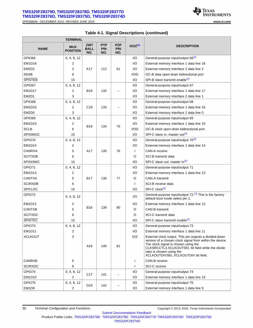
30
TMS320F28379D, TMS320F28378D, TMS320F28377DTMS320F28376D, TMS320F28375D, TMS320F28374DSPRS880M –DECEMBER 2013–REVISED JUNE 2020 www.ti.com
Submit Documentation FeedbackProduct Folder Links: TMS320F28379D TMS320F28378D TMS320F28377D TMS320F28376D TMS320F28375D
TMS320F28374D
Terminal Configuration and Functions Copyright © 2013–2020, Texas Instruments Incorporated
Table 4-1. Signal Descriptions (continued)TERMINAL
I/O/Z(1) DESCRIPTIONNAME MUX
POSITIONZWTBALLNO.
PTPPINNO.
PZPPINNO.
GPIO66 0, 4, 8, 12
K17 112 61
I/O General-purpose input/output 66(3)
EM1D18 2 I/O External memory interface 1 data line 18EM2D2 3 I/O External memory interface 2 data line 2SDAB 6 I/OD I2C-B data open-drain bidirectional portSPISTEB 15 I/O SPI-B slave transmit enable(2)
GPIO67 0, 4, 8, 12B19 132 –
I/O General-purpose input/output 67EM1D17 2 I/O External memory interface 1 data line 17EM2D1 3 I/O External memory interface 2 data line 1GPIO68 0, 4, 8, 12
C18 133 –I/O General-purpose input/output 68
EM1D16 2 I/O External memory interface 1 data line 16EM2D0 3 I/O External memory interface 2 data line 0GPIO69 0, 4, 8, 12
B18 134 75
I/O General-purpose input/output 69EM1D15 2 I/O External memory interface 1 data line 15SCLB 6 I/OD I2C-B clock open-drain bidirectional portSPISIMOC 15 I/O SPI-C slave in, master out(2)
GPIO70 0, 4, 8, 12
A17 135 76
I/O General-purpose input/output 70(3)
EM1D14 2 I/O External memory interface 1 data line 14CANRXA 5 I CAN-A receiveSCITXDB 6 O SCI-B transmit dataSPISOMIC 15 I/O SPI-C slave out, master in(2)
GPIO71 0, 4, 8, 12
B17 136 77
I/O General-purpose input/output 71EM1D13 2 I/O External memory interface 1 data line 13CANTXA 5 O CAN-A transmitSCIRXDB 6 I SCI-B receive dataSPICLKC 15 I/O SPI-C clock(2)
GPIO72 0, 4, 8, 12
B16 139 80
I/O General-purpose input/output 72.(3) This is the factorydefault boot mode select pin 1.
EM1D12 2 I/O External memory interface 1 data line 12CANTXB 5 O CAN-B transmitSCITXDC 6 O SCI-C transmit dataSPISTEC 15 I/O SPI-C slave transmit enable(2)
GPIO73 0, 4, 8, 12
A16 140 81
I/O General-purpose input/output 73EM1D11 2 I/O External memory interface 1 data line 11XCLKOUT 3 O/Z External clock output. This pin outputs a divided-down
version of a chosen clock signal from within the device.The clock signal is chosen using theCLKSRCCTL3.XCLKOUTSEL bit field while the divideratio is chosen using theXCLKOUTDIVSEL.XCLKOUTDIV bit field.
CANRXB 5 I CAN-B receiveSCIRXDC 6 I SCI-C receiveGPIO74 0, 4, 8, 12
C17 141 –I/O General-purpose input/output 74
EM1D10 2 I/O External memory interface 1 data line 10GPIO75 0, 4, 8, 12
D16 142 –I/O General-purpose input/output 75
EM1D9 2 I/O External memory interface 1 data line 9
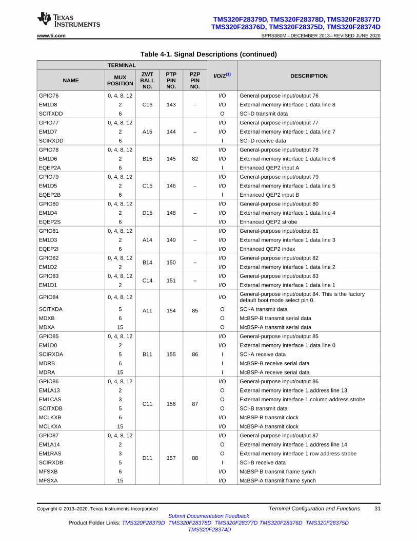
31
TMS320F28379D, TMS320F28378D, TMS320F28377DTMS320F28376D, TMS320F28375D, TMS320F28374D
www.ti.com SPRS880M –DECEMBER 2013–REVISED JUNE 2020
Submit Documentation FeedbackProduct Folder Links: TMS320F28379D TMS320F28378D TMS320F28377D TMS320F28376D TMS320F28375D
TMS320F28374D
Terminal Configuration and FunctionsCopyright © 2013–2020, Texas Instruments Incorporated
Table 4-1. Signal Descriptions (continued)TERMINAL
I/O/Z(1) DESCRIPTIONNAME MUX
POSITIONZWTBALLNO.
PTPPINNO.
PZPPINNO.
GPIO76 0, 4, 8, 12C16 143 –
I/O General-purpose input/output 76EM1D8 2 I/O External memory interface 1 data line 8SCITXDD 6 O SCI-D transmit dataGPIO77 0, 4, 8, 12
A15 144 –I/O General-purpose input/output 77
EM1D7 2 I/O External memory interface 1 data line 7SCIRXDD 6 I SCI-D receive dataGPIO78 0, 4, 8, 12
B15 145 82I/O General-purpose input/output 78
EM1D6 2 I/O External memory interface 1 data line 6EQEP2A 6 I Enhanced QEP2 input AGPIO79 0, 4, 8, 12
C15 146 –I/O General-purpose input/output 79
EM1D5 2 I/O External memory interface 1 data line 5EQEP2B 6 I Enhanced QEP2 input BGPIO80 0, 4, 8, 12
D15 148 –I/O General-purpose input/output 80
EM1D4 2 I/O External memory interface 1 data line 4EQEP2S 6 I/O Enhanced QEP2 strobeGPIO81 0, 4, 8, 12
A14 149 –I/O General-purpose input/output 81
EM1D3 2 I/O External memory interface 1 data line 3EQEP2I 6 I/O Enhanced QEP2 indexGPIO82 0, 4, 8, 12
B14 150 –I/O General-purpose input/output 82
EM1D2 2 I/O External memory interface 1 data line 2GPIO83 0, 4, 8, 12
C14 151 –I/O General-purpose input/output 83
EM1D1 2 I/O External memory interface 1 data line 1
GPIO84 0, 4, 8, 12
A11 154 85
I/O General-purpose input/output 84. This is the factorydefault boot mode select pin 0.
SCITXDA 5 O SCI-A transmit dataMDXB 6 O McBSP-B transmit serial dataMDXA 15 O McBSP-A transmit serial dataGPIO85 0, 4, 8, 12
B11 155 86
I/O General-purpose input/output 85EM1D0 2 I/O External memory interface 1 data line 0SCIRXDA 5 I SCI-A receive dataMDRB 6 I McBSP-B receive serial dataMDRA 15 I McBSP-A receive serial dataGPIO86 0, 4, 8, 12
C11 156 87
I/O General-purpose input/output 86EM1A13 2 O External memory interface 1 address line 13EM1CAS 3 O External memory interface 1 column address strobeSCITXDB 5 O SCI-B transmit dataMCLKXB 6 I/O McBSP-B transmit clockMCLKXA 15 I/O McBSP-A transmit clockGPIO87 0, 4, 8, 12
D11 157 88
I/O General-purpose input/output 87EM1A14 2 O External memory interface 1 address line 14EM1RAS 3 O External memory interface 1 row address strobeSCIRXDB 5 I SCI-B receive dataMFSXB 6 I/O McBSP-B transmit frame synchMFSXA 15 I/O McBSP-A transmit frame synch
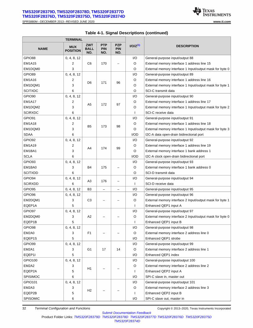
32
TMS320F28379D, TMS320F28378D, TMS320F28377DTMS320F28376D, TMS320F28375D, TMS320F28374DSPRS880M –DECEMBER 2013–REVISED JUNE 2020 www.ti.com
Submit Documentation FeedbackProduct Folder Links: TMS320F28379D TMS320F28378D TMS320F28377D TMS320F28376D TMS320F28375D
TMS320F28374D
Terminal Configuration and Functions Copyright © 2013–2020, Texas Instruments Incorporated
Table 4-1. Signal Descriptions (continued)TERMINAL
I/O/Z(1) DESCRIPTIONNAME MUX
POSITIONZWTBALLNO.
PTPPINNO.
PZPPINNO.
GPIO88 0, 4, 8, 12C6 170 –
I/O General-purpose input/output 88EM1A15 2 O External memory interface 1 address line 15EM1DQM0 3 O External memory interface 1 Input/output mask for byte 0GPIO89 0, 4, 8, 12
D6 171 96
I/O General-purpose input/output 89EM1A16 2 O External memory interface 1 address line 16EM1DQM1 3 O External memory interface 1 Input/output mask for byte 1SCITXDC 6 O SCI-C transmit dataGPIO90 0, 4, 8, 12
A5 172 97
I/O General-purpose input/output 90EM1A17 2 O External memory interface 1 address line 17EM1DQM2 3 O External memory interface 1 Input/output mask for byte 2SCIRXDC 6 I SCI-C receive dataGPIO91 0, 4, 8, 12
B5 173 98
I/O General-purpose input/output 91EM1A18 2 O External memory interface 1 address line 18EM1DQM3 3 O External memory interface 1 Input/output mask for byte 3SDAA 6 I/OD I2C-A data open-drain bidirectional portGPIO92 0, 4, 8, 12
A4 174 99
I/O General-purpose input/output 92EM1A19 2 O External memory interface 1 address line 19EM1BA1 3 O External memory interface 1 bank address 1SCLA 6 I/OD I2C-A clock open-drain bidirectional portGPIO93 0, 4, 8, 12
B4 175 –I/O General-purpose input/output 93
EM1BA0 3 O External memory interface 1 bank address 0SCITXDD 6 O SCI-D transmit dataGPIO94 0, 4, 8, 12
A3 176 –I/O General-purpose input/output 94
SCIRXDD 6 I SCI-D receive dataGPIO95 0, 4, 8, 12 B3 – – I/O General-purpose input/output 95GPIO96 0, 4, 8, 12
C3 – –I/O General-purpose input/output 96
EM2DQM1 3 O External memory interface 2 Input/output mask for byte 1EQEP1A 5 I Enhanced QEP1 input AGPIO97 0, 4, 8, 12
A2 – –I/O General-purpose input/output 97
EM2DQM0 3 O External memory interface 2 Input/output mask for byte 0EQEP1B 5 I Enhanced QEP1 input BGPIO98 0, 4, 8, 12
F1 – –I/O General-purpose input/output 98
EM2A0 3 O External memory interface 2 address line 0EQEP1S 5 I/O Enhanced QEP1 strobeGPIO99 0, 4, 8, 12
G1 17 14I/O General-purpose input/output 99
EM2A1 3 O External memory interface 2 address line 1EQEP1I 5 I/O Enhanced QEP1 indexGPIO100 0, 4, 8, 12
H1 – –
I/O General-purpose input/output 100EM2A2 3 O External memory interface 2 address line 2EQEP2A 5 I Enhanced QEP2 input ASPISIMOC 6 I/O SPI-C slave in, master outGPIO101 0, 4, 8, 12
H2 – –
I/O General-purpose input/output 101EM2A3 3 O External memory interface 2 address line 3EQEP2B 5 I Enhanced QEP2 input BSPISOMIC 6 I/O SPI-C slave out, master in
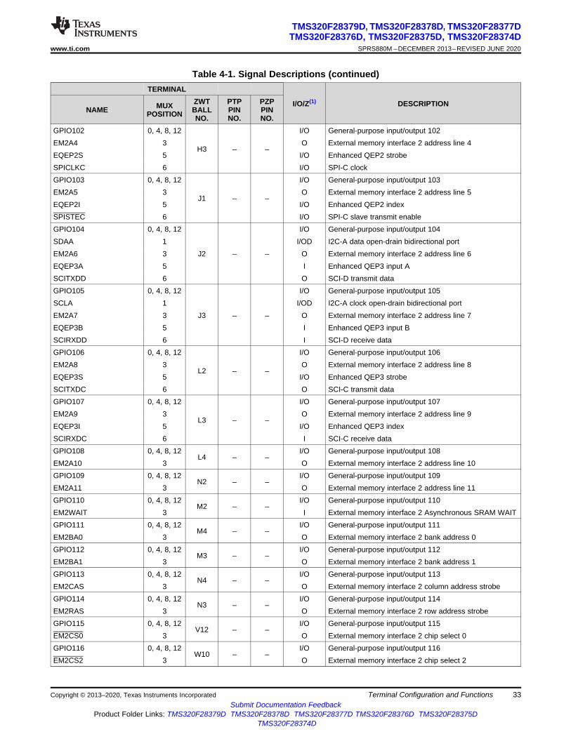
33
TMS320F28379D, TMS320F28378D, TMS320F28377DTMS320F28376D, TMS320F28375D, TMS320F28374D
www.ti.com SPRS880M –DECEMBER 2013–REVISED JUNE 2020
Submit Documentation FeedbackProduct Folder Links: TMS320F28379D TMS320F28378D TMS320F28377D TMS320F28376D TMS320F28375D
TMS320F28374D
Terminal Configuration and FunctionsCopyright © 2013–2020, Texas Instruments Incorporated
Table 4-1. Signal Descriptions (continued)TERMINAL
I/O/Z(1) DESCRIPTIONNAME MUX
POSITIONZWTBALLNO.
PTPPINNO.
PZPPINNO.
GPIO102 0, 4, 8, 12
H3 – –
I/O General-purpose input/output 102EM2A4 3 O External memory interface 2 address line 4EQEP2S 5 I/O Enhanced QEP2 strobeSPICLKC 6 I/O SPI-C clockGPIO103 0, 4, 8, 12
J1 – –
I/O General-purpose input/output 103EM2A5 3 O External memory interface 2 address line 5EQEP2I 5 I/O Enhanced QEP2 indexSPISTEC 6 I/O SPI-C slave transmit enableGPIO104 0, 4, 8, 12
J2 – –
I/O General-purpose input/output 104SDAA 1 I/OD I2C-A data open-drain bidirectional portEM2A6 3 O External memory interface 2 address line 6EQEP3A 5 I Enhanced QEP3 input ASCITXDD 6 O SCI-D transmit dataGPIO105 0, 4, 8, 12
J3 – –
I/O General-purpose input/output 105SCLA 1 I/OD I2C-A clock open-drain bidirectional portEM2A7 3 O External memory interface 2 address line 7EQEP3B 5 I Enhanced QEP3 input BSCIRXDD 6 I SCI-D receive dataGPIO106 0, 4, 8, 12
L2 – –
I/O General-purpose input/output 106EM2A8 3 O External memory interface 2 address line 8EQEP3S 5 I/O Enhanced QEP3 strobeSCITXDC 6 O SCI-C transmit dataGPIO107 0, 4, 8, 12
L3 – –
I/O General-purpose input/output 107EM2A9 3 O External memory interface 2 address line 9EQEP3I 5 I/O Enhanced QEP3 indexSCIRXDC 6 I SCI-C receive dataGPIO108 0, 4, 8, 12
L4 – –I/O General-purpose input/output 108
EM2A10 3 O External memory interface 2 address line 10GPIO109 0, 4, 8, 12
N2 – –I/O General-purpose input/output 109
EM2A11 3 O External memory interface 2 address line 11GPIO110 0, 4, 8, 12
M2 – –I/O General-purpose input/output 110
EM2WAIT 3 I External memory interface 2 Asynchronous SRAM WAITGPIO111 0, 4, 8, 12
M4 – –I/O General-purpose input/output 111
EM2BA0 3 O External memory interface 2 bank address 0GPIO112 0, 4, 8, 12
M3 – –I/O General-purpose input/output 112
EM2BA1 3 O External memory interface 2 bank address 1GPIO113 0, 4, 8, 12
N4 – –I/O General-purpose input/output 113
EM2CAS 3 O External memory interface 2 column address strobeGPIO114 0, 4, 8, 12
N3 – –I/O General-purpose input/output 114
EM2RAS 3 O External memory interface 2 row address strobeGPIO115 0, 4, 8, 12
V12 – –I/O General-purpose input/output 115
EM2CS0 3 O External memory interface 2 chip select 0GPIO116 0, 4, 8, 12
W10 – –I/O General-purpose input/output 116
EM2CS2 3 O External memory interface 2 chip select 2
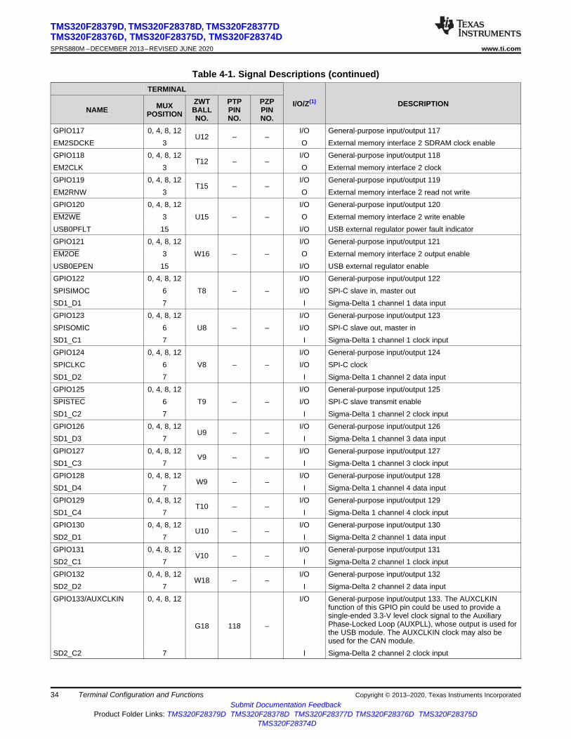
34
TMS320F28379D, TMS320F28378D, TMS320F28377DTMS320F28376D, TMS320F28375D, TMS320F28374DSPRS880M –DECEMBER 2013–REVISED JUNE 2020 www.ti.com
Submit Documentation FeedbackProduct Folder Links: TMS320F28379D TMS320F28378D TMS320F28377D TMS320F28376D TMS320F28375D
TMS320F28374D
Terminal Configuration and Functions Copyright © 2013–2020, Texas Instruments Incorporated
Table 4-1. Signal Descriptions (continued)TERMINAL
I/O/Z(1) DESCRIPTIONNAME MUX
POSITIONZWTBALLNO.
PTPPINNO.
PZPPINNO.
GPIO117 0, 4, 8, 12U12 – –
I/O General-purpose input/output 117EM2SDCKE 3 O External memory interface 2 SDRAM clock enableGPIO118 0, 4, 8, 12
T12 – –I/O General-purpose input/output 118
EM2CLK 3 O External memory interface 2 clockGPIO119 0, 4, 8, 12
T15 – –I/O General-purpose input/output 119
EM2RNW 3 O External memory interface 2 read not writeGPIO120 0, 4, 8, 12
U15 – –I/O General-purpose input/output 120
EM2WE 3 O External memory interface 2 write enableUSB0PFLT 15 I/O USB external regulator power fault indicatorGPIO121 0, 4, 8, 12
W16 – –I/O General-purpose input/output 121
EM2OE 3 O External memory interface 2 output enableUSB0EPEN 15 I/O USB external regulator enableGPIO122 0, 4, 8, 12
T8 – –I/O General-purpose input/output 122
SPISIMOC 6 I/O SPI-C slave in, master outSD1_D1 7 I Sigma-Delta 1 channel 1 data inputGPIO123 0, 4, 8, 12
U8 – –I/O General-purpose input/output 123
SPISOMIC 6 I/O SPI-C slave out, master inSD1_C1 7 I Sigma-Delta 1 channel 1 clock inputGPIO124 0, 4, 8, 12
V8 – –I/O General-purpose input/output 124
SPICLKC 6 I/O SPI-C clockSD1_D2 7 I Sigma-Delta 1 channel 2 data inputGPIO125 0, 4, 8, 12
T9 – –I/O General-purpose input/output 125
SPISTEC 6 I/O SPI-C slave transmit enableSD1_C2 7 I Sigma-Delta 1 channel 2 clock inputGPIO126 0, 4, 8, 12
U9 – –I/O General-purpose input/output 126
SD1_D3 7 I Sigma-Delta 1 channel 3 data inputGPIO127 0, 4, 8, 12
V9 – –I/O General-purpose input/output 127
SD1_C3 7 I Sigma-Delta 1 channel 3 clock inputGPIO128 0, 4, 8, 12
W9 – –I/O General-purpose input/output 128
SD1_D4 7 I Sigma-Delta 1 channel 4 data inputGPIO129 0, 4, 8, 12
T10 – –I/O General-purpose input/output 129
SD1_C4 7 I Sigma-Delta 1 channel 4 clock inputGPIO130 0, 4, 8, 12
U10 – –I/O General-purpose input/output 130
SD2_D1 7 I Sigma-Delta 2 channel 1 data inputGPIO131 0, 4, 8, 12
V10 – –I/O General-purpose input/output 131
SD2_C1 7 I Sigma-Delta 2 channel 1 clock inputGPIO132 0, 4, 8, 12
W18 – –I/O General-purpose input/output 132
SD2_D2 7 I Sigma-Delta 2 channel 2 data inputGPIO133/AUXCLKIN 0, 4, 8, 12
G18 118 –
I/O General-purpose input/output 133. The AUXCLKINfunction of this GPIO pin could be used to provide asingle-ended 3.3-V level clock signal to the AuxiliaryPhase-Locked Loop (AUXPLL), whose output is used forthe USB module. The AUXCLKIN clock may also beused for the CAN module.
SD2_C2 7 I Sigma-Delta 2 channel 2 clock input

35
TMS320F28379D, TMS320F28378D, TMS320F28377DTMS320F28376D, TMS320F28375D, TMS320F28374D
www.ti.com SPRS880M –DECEMBER 2013–REVISED JUNE 2020
Submit Documentation FeedbackProduct Folder Links: TMS320F28379D TMS320F28378D TMS320F28377D TMS320F28376D TMS320F28375D
TMS320F28374D
Terminal Configuration and FunctionsCopyright © 2013–2020, Texas Instruments Incorporated
Table 4-1. Signal Descriptions (continued)TERMINAL
I/O/Z(1) DESCRIPTIONNAME MUX
POSITIONZWTBALLNO.
PTPPINNO.
PZPPINNO.
GPIO134 0, 4, 8, 12V18 – –
I/O General-purpose input/output 134SD2_D3 7 I Sigma-Delta 2 channel 3 data inputGPIO135 0, 4, 8, 12
U18 – –I/O General-purpose input/output 135
SCITXDA 6 O SCI-A transmit dataSD2_C3 7 I Sigma-Delta 2 channel 3 clock inputGPIO136 0, 4, 8, 12
T17 – –I/O General-purpose input/output 136
SCIRXDA 6 I SCI-A receive dataSD2_D4 7 I Sigma-Delta 2 channel 4 data inputGPIO137 0, 4, 8, 12
T18 – –I/O General-purpose input/output 137
SCITXDB 6 O SCI-B transmit dataSD2_C4 7 I Sigma-Delta 2 channel 4 clock inputGPIO138 0, 4, 8, 12
T19 – –I/O General-purpose input/output 138
SCIRXDB 6 I SCI-B receive dataGPIO139 0, 4, 8, 12
N19 – –I/O General-purpose input/output 139
SCIRXDC 6 I SCI-C receive dataGPIO140 0, 4, 8, 12
M19 – –I/O General-purpose input/output 140
SCITXDC 6 O SCI-C transmit dataGPIO141 0, 4, 8, 12
M18 – –I/O General-purpose input/output 141
SCIRXDD 6 I SCI-D receive dataGPIO142 0, 4, 8, 12
L19 – –I/O General-purpose input/output 142
SCITXDD 6 O SCI-D transmit dataGPIO143 0, 4, 8, 12 F18 – – I/O General-purpose input/output 143GPIO144 0, 4, 8, 12 F17 – – I/O General-purpose input/output 144GPIO145 0, 4, 8, 12
E17 – –I/O General-purpose input/output 145
EPWM1A 1 O Enhanced PWM1 output A (HRPWM-capable)GPIO146 0, 4, 8, 12
D18 – –I/O General-purpose input/output 146
EPWM1B 1 O Enhanced PWM1 output B (HRPWM-capable)GPIO147 0, 4, 8, 12
D17 – –I/O General-purpose input/output 147
EPWM2A 1 O Enhanced PWM2 output A (HRPWM-capable)GPIO148 0, 4, 8, 12
D14 – –I/O General-purpose input/output 148
EPWM2B 1 O Enhanced PWM2 output B (HRPWM-capable)GPIO149 0, 4, 8, 12
A13 – –I/O General-purpose input/output 149
EPWM3A 1 O Enhanced PWM3 output A (HRPWM-capable)GPIO150 0, 4, 8, 12
B13 – –I/O General-purpose input/output 150
EPWM3B 1 O Enhanced PWM3 output B (HRPWM-capable)GPIO151 0, 4, 8, 12
C13 – –I/O General-purpose input/output 151
EPWM4A 1 O Enhanced PWM4 output A (HRPWM-capable)GPIO152 0, 4, 8, 12
D13 – –I/O General-purpose input/output 152
EPWM4B 1 O Enhanced PWM4 output B (HRPWM-capable)GPIO153 0, 4, 8, 12
A12 – –I/O General-purpose input/output 153
EPWM5A 1 O Enhanced PWM5 output A (HRPWM-capable)GPIO154 0, 4, 8, 12
B12 – –I/O General-purpose input/output 154
EPWM5B 1 O Enhanced PWM5 output B (HRPWM-capable)GPIO155 0, 4, 8, 12
C12 – –I/O General-purpose input/output 155
EPWM6A 1 O Enhanced PWM6 output A (HRPWM-capable)
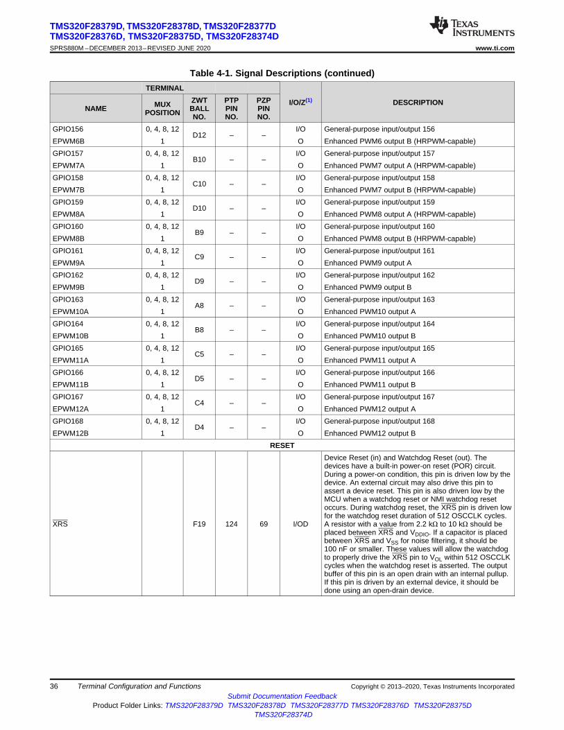
36
TMS320F28379D, TMS320F28378D, TMS320F28377DTMS320F28376D, TMS320F28375D, TMS320F28374DSPRS880M –DECEMBER 2013–REVISED JUNE 2020 www.ti.com
Submit Documentation FeedbackProduct Folder Links: TMS320F28379D TMS320F28378D TMS320F28377D TMS320F28376D TMS320F28375D
TMS320F28374D
Terminal Configuration and Functions Copyright © 2013–2020, Texas Instruments Incorporated
Table 4-1. Signal Descriptions (continued)TERMINAL
I/O/Z(1) DESCRIPTIONNAME MUX
POSITIONZWTBALLNO.
PTPPINNO.
PZPPINNO.
GPIO156 0, 4, 8, 12D12 – –
I/O General-purpose input/output 156EPWM6B 1 O Enhanced PWM6 output B (HRPWM-capable)GPIO157 0, 4, 8, 12
B10 – –I/O General-purpose input/output 157
EPWM7A 1 O Enhanced PWM7 output A (HRPWM-capable)GPIO158 0, 4, 8, 12
C10 – –I/O General-purpose input/output 158
EPWM7B 1 O Enhanced PWM7 output B (HRPWM-capable)GPIO159 0, 4, 8, 12
D10 – –I/O General-purpose input/output 159
EPWM8A 1 O Enhanced PWM8 output A (HRPWM-capable)GPIO160 0, 4, 8, 12
B9 – –I/O General-purpose input/output 160
EPWM8B 1 O Enhanced PWM8 output B (HRPWM-capable)GPIO161 0, 4, 8, 12
C9 – –I/O General-purpose input/output 161
EPWM9A 1 O Enhanced PWM9 output AGPIO162 0, 4, 8, 12
D9 – –I/O General-purpose input/output 162
EPWM9B 1 O Enhanced PWM9 output BGPIO163 0, 4, 8, 12
A8 – –I/O General-purpose input/output 163
EPWM10A 1 O Enhanced PWM10 output AGPIO164 0, 4, 8, 12
B8 – –I/O General-purpose input/output 164
EPWM10B 1 O Enhanced PWM10 output BGPIO165 0, 4, 8, 12
C5 – –I/O General-purpose input/output 165
EPWM11A 1 O Enhanced PWM11 output AGPIO166 0, 4, 8, 12
D5 – –I/O General-purpose input/output 166
EPWM11B 1 O Enhanced PWM11 output BGPIO167 0, 4, 8, 12
C4 – –I/O General-purpose input/output 167
EPWM12A 1 O Enhanced PWM12 output AGPIO168 0, 4, 8, 12
D4 – –I/O General-purpose input/output 168
EPWM12B 1 O Enhanced PWM12 output BRESET
XRS F19 124 69 I/OD
Device Reset (in) and Watchdog Reset (out). Thedevices have a built-in power-on reset (POR) circuit.During a power-on condition, this pin is driven low by thedevice. An external circuit may also drive this pin toassert a device reset. This pin is also driven low by theMCU when a watchdog reset or NMI watchdog resetoccurs. During watchdog reset, the XRS pin is driven lowfor the watchdog reset duration of 512 OSCCLK cycles.A resistor with a value from 2.2 kΩ to 10 kΩ should beplaced between XRS and VDDIO. If a capacitor is placedbetween XRS and VSS for noise filtering, it should be100 nF or smaller. These values will allow the watchdogto properly drive the XRS pin to VOL within 512 OSCCLKcycles when the watchdog reset is asserted. The outputbuffer of this pin is an open drain with an internal pullup.If this pin is driven by an external device, it should bedone using an open-drain device.

37
TMS320F28379D, TMS320F28378D, TMS320F28377DTMS320F28376D, TMS320F28375D, TMS320F28374D
www.ti.com SPRS880M –DECEMBER 2013–REVISED JUNE 2020
Submit Documentation FeedbackProduct Folder Links: TMS320F28379D TMS320F28378D TMS320F28377D TMS320F28376D TMS320F28375D
TMS320F28374D
Terminal Configuration and FunctionsCopyright © 2013–2020, Texas Instruments Incorporated
Table 4-1. Signal Descriptions (continued)TERMINAL
I/O/Z(1) DESCRIPTIONNAME MUX
POSITIONZWTBALLNO.
PTPPINNO.
PZPPINNO.
CLOCKS
X1 G19 123 68 I
On-chip crystal-oscillator input. To use this oscillator, aquartz crystal must be connected across X1 and X2. Ifthis pin is not used, it must be tied to GND.This pin can also be used to feed a single-ended 3.3-Vlevel clock. In this case, X2 is a No Connect (NC).
X2 J19 121 66 OOn-chip crystal-oscillator output. A quartz crystal may beconnected across X1 and X2. If X2 is not used, it mustbe left unconnected.
NO CONNECT
NC H4 – – No connect. BGA ball is electrically open and notconnected to the die.
JTAGTCK V15 81 50 I JTAG test clock with internal pullup (see Section 5.6)
TDI W13 77 46 IJTAG test data input (TDI) with internal pullup. TDI isclocked into the selected register (instruction or data) ona rising edge of TCK.
TDO W15 78 47 O/ZJTAG scan out, test data output (TDO). The contents ofthe selected register (instruction or data) are shifted outof TDO on the falling edge of TCK.(3)
TMS W14 80 49 IJTAG test-mode select (TMS) with internal pullup. Thisserial control input is clocked into the TAP controller onthe rising edge of TCK.
TRST V14 79 48 I
JTAG test reset with internal pulldown. TRST, whendriven high, gives the scan system control of theoperations of the device. If this signal is driven low, thedevice operates in its functional mode, and the test resetsignals are ignored. NOTE: TRST must be maintainedlow at all times during normal device operation. Anexternal pulldown resistor is required on this pin. Thevalue of this resistor should be based on drive strengthof the debugger pods applicable to the design. A 2.2-kΩor smaller resistor generally offers adequate protection.The value of the resistor is application-specific. TIrecommends that each target board be validated forproper operation of the debugger and the application.This pin has an internal 50-ns (nominal) glitch filter.
INTERNAL VOLTAGE REGULATOR CONTROL
VREGENZ J18 119 64 IInternal voltage regulator enable with internal pulldown.The internal VREG is not supported and must bedisabled. Connect VREGENZ to VDDIO.
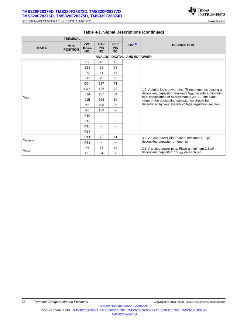
38
TMS320F28379D, TMS320F28378D, TMS320F28377DTMS320F28376D, TMS320F28375D, TMS320F28374DSPRS880M –DECEMBER 2013–REVISED JUNE 2020 www.ti.com
Submit Documentation FeedbackProduct Folder Links: TMS320F28379D TMS320F28378D TMS320F28377D TMS320F28376D TMS320F28375D
TMS320F28374D
Terminal Configuration and Functions Copyright © 2013–2020, Texas Instruments Incorporated
Table 4-1. Signal Descriptions (continued)TERMINAL
I/O/Z(1) DESCRIPTIONNAME MUX
POSITIONZWTBALLNO.
PTPPINNO.
PZPPINNO.
ANALOG, DIGITAL, AND I/O POWER
VDD
E9 16 16
1.2-V digital logic power pins. TI recommends placing adecoupling capacitor near each VDD pin with a minimumtotal capacitance of approximately 20 uF. The exactvalue of the decoupling capacitance should bedetermined by your system voltage regulation solution.
E11 21 39F9 61 45F11 76 63G14 117 71G15 126 78J14 137 84J15 153 89K5 158 95K6 169 –P10 – –P13 – –R10 – –R13 – –
VDD3VFLR11 72 41 3.3-V Flash power pin. Place a minimum 0.1-µF
decoupling capacitor on each pin.R12 – –
VDDAP6 36 18 3.3-V analog power pins. Place a minimum 2.2-µF
decoupling capacitor to VSSA on each pin.R6 54 38

39
TMS320F28379D, TMS320F28378D, TMS320F28377DTMS320F28376D, TMS320F28375D, TMS320F28374D
www.ti.com SPRS880M –DECEMBER 2013–REVISED JUNE 2020
Submit Documentation FeedbackProduct Folder Links: TMS320F28379D TMS320F28378D TMS320F28377D TMS320F28376D TMS320F28375D
TMS320F28374D
Terminal Configuration and FunctionsCopyright © 2013–2020, Texas Instruments Incorporated
Table 4-1. Signal Descriptions (continued)TERMINAL
I/O/Z(1) DESCRIPTIONNAME MUX
POSITIONZWTBALLNO.
PTPPINNO.
PZPPINNO.
VDDIO
A9 3 2
3.3-V digital I/O power pins. Place a minimum 0.1-µFdecoupling capacitor on each pin. The exact value of thedecoupling capacitance should be determined by yoursystem voltage regulation solution.
A18 11 10B1 15 15E7 20 40E10 26 44E13 62 55E16 68 62F4 75 72F7 82 79F10 88 83F13 91 90F16 99 94G4 106 –G5 114 –G6 116 –H5 127 –H6 138 –L14 147 –L15 152 –M1 159 –M5 168 –M6 – –N14 – –N15 – –P9 – –R9 – –V19 – –W8 – –
VDDOSC
H16 120 65 Power pins for the 3.3-V on-chip crystal oscillator (X1and X2) and the two zero-pin internal oscillators(INTOSC). Place a 0.1-μF (minimum) decouplingcapacitor on each pin.
H17 125 70

40
TMS320F28379D, TMS320F28378D, TMS320F28377DTMS320F28376D, TMS320F28375D, TMS320F28374DSPRS880M –DECEMBER 2013–REVISED JUNE 2020 www.ti.com
Submit Documentation FeedbackProduct Folder Links: TMS320F28379D TMS320F28378D TMS320F28377D TMS320F28376D TMS320F28375D
TMS320F28374D
Terminal Configuration and Functions Copyright © 2013–2020, Texas Instruments Incorporated
Table 4-1. Signal Descriptions (continued)TERMINAL
I/O/Z(1) DESCRIPTIONNAME MUX
POSITIONZWTBALLNO.
PTPPINNO.
PZPPINNO.
VSS
A1
PWRPAD
PWRPAD
Device ground. For Quad Flatpacks (QFPs), thePowerPAD on the bottom of the package must besoldered to the ground plane of the PCB.
A10A19E5E6E8E12E14E15F5F6F8F12F14F15G16G17H8H9H10H11H12H14H15J5J6J8J9J10J11J12K8K9K10K11K12K14K15L5L6L8L9
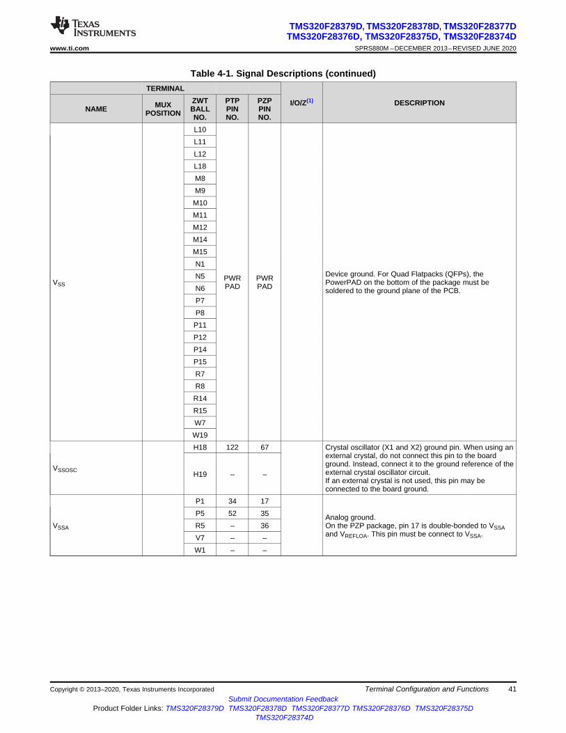
41
TMS320F28379D, TMS320F28378D, TMS320F28377DTMS320F28376D, TMS320F28375D, TMS320F28374D
www.ti.com SPRS880M –DECEMBER 2013–REVISED JUNE 2020
Submit Documentation FeedbackProduct Folder Links: TMS320F28379D TMS320F28378D TMS320F28377D TMS320F28376D TMS320F28375D
TMS320F28374D
Terminal Configuration and FunctionsCopyright © 2013–2020, Texas Instruments Incorporated
Table 4-1. Signal Descriptions (continued)TERMINAL
I/O/Z(1) DESCRIPTIONNAME MUX
POSITIONZWTBALLNO.
PTPPINNO.
PZPPINNO.
VSS
L10
PWRPAD
PWRPAD
Device ground. For Quad Flatpacks (QFPs), thePowerPAD on the bottom of the package must besoldered to the ground plane of the PCB.
L11L12L18M8M9
M10M11M12M14M15N1N5N6P7P8P11P12P14P15R7R8R14R15W7W19
VSSOSC
H18 122 67 Crystal oscillator (X1 and X2) ground pin. When using anexternal crystal, do not connect this pin to the boardground. Instead, connect it to the ground reference of theexternal crystal oscillator circuit.If an external crystal is not used, this pin may beconnected to the board ground.
H19 – –
VSSA
P1 34 17
Analog ground.On the PZP package, pin 17 is double-bonded to VSSAand VREFLOA. This pin must be connect to VSSA.
P5 52 35R5 – 36V7 – –W1 – –

42
TMS320F28379D, TMS320F28378D, TMS320F28377DTMS320F28376D, TMS320F28375D, TMS320F28374DSPRS880M –DECEMBER 2013–REVISED JUNE 2020 www.ti.com
Submit Documentation FeedbackProduct Folder Links: TMS320F28379D TMS320F28378D TMS320F28377D TMS320F28376D TMS320F28375D
TMS320F28374D
Terminal Configuration and Functions Copyright © 2013–2020, Texas Instruments Incorporated
Table 4-1. Signal Descriptions (continued)TERMINAL
I/O/Z(1) DESCRIPTIONNAME MUX
POSITIONZWTBALLNO.
PTPPINNO.
PZPPINNO.
SPECIAL FUNCTIONSERRORSTS U19 92 – O Error status output. This pin has an internal pulldown.
TEST PINS
FLT1 W12 73 42 I/O Flash test pin 1. Reserved for TI. Must be leftunconnected.
FLT2 V13 74 43 I/O Flash test pin 2. Reserved for TI. Must be leftunconnected.
(1) Pins not bonded out in a given package will have the internal pullups enabled by the Boot ROM.
(1) I = Input, O = Output, OD = Open Drain, Z = High Impedance(2) High-Speed SPI-enabled GPIO mux option. This pin mux option is required when using the SPI in High-Speed Mode (HS_MODE = 1 in
SPICCR). This mux option is still available when not using the SPI in High-Speed Mode (HS_MODE = 0 in SPICCR).(3) This pin has output impedance that can be as low as 22 Ω. This output could have fast edges and ringing depending on the system
PCB characteristics. If this is a concern, the user should take precautions such as adding a 39Ω (10% tolerance) series terminationresistor or implement some other termination scheme. It is also recommended that a system-level signal integrity analysis be performedwith the provided IBIS models. The termination is not required if this pin is used for input function.
4.3 Pins With Internal Pullup and PulldownSome pins on the device have internal pullups or pulldowns. Table 4-2 lists the pull direction and when itis active. The pullups on GPIO pins are disabled by default and can be enabled through software. In orderto avoid any floating unbonded inputs, the Boot ROM will enable internal pullups on GPIO pins that arenot bonded out in a particular package. Other pins noted in Table 4-2 with pullups and pulldowns arealways on and cannot be disabled.
Table 4-2. Pins With Internal Pullup and Pulldown
PIN RESET(XRS = 0) DEVICE BOOT APPLICATION SOFTWARE
GPIOx Pullup disabled Pullup disabled (1) Pullup enable is application-defined
TRST Pulldown activeTCK Pullup activeTMS Pullup activeTDI Pullup activeXRS Pullup activeVREGENZ Pulldown activeERRORSTS Pulldown activeOther pins No pullup or pulldown present

43
TMS320F28379D, TMS320F28378D, TMS320F28377DTMS320F28376D, TMS320F28375D, TMS320F28374D
www.ti.com SPRS880M –DECEMBER 2013–REVISED JUNE 2020
Submit Documentation FeedbackProduct Folder Links: TMS320F28379D TMS320F28378D TMS320F28377D TMS320F28376D TMS320F28375D
TMS320F28374D
Terminal Configuration and FunctionsCopyright © 2013–2020, Texas Instruments Incorporated
(1) I = Input, O = Output, OD = Open Drain(2) GPIO Index settings of 9, 10, 11, 13, and 14 are reserved.
4.4 Pin Multiplexing
4.4.1 GPIO Muxed PinsTable 4-3 shows the GPIO muxed pins. The default for each pin is the GPIO function, secondary functionscan be selected by setting both the GPyGMUXn.GPIOz and GPyMUXn.GPIOz register bits. TheGPyGMUXn register should be configured prior to the GPyMUXn to avoid transient pulses on GPIO's fromalternate mux selections. Columns not shown and blank cells are reserved GPIO Mux settings.
Table 4-3. GPIO Muxed Pins (1) (2)
GPIO Mux Selection
GPIO Index 0, 4, 8, 12 1 2 3 5 6 7 15
GPyGMUXn.GPIOz =
00b, 01b,10b, 11b 00b 01b 11b
GPyMUXn.GPIOz = 00b 01b 10b 11b 01b 10b 11b 11b
GPIO0 EPWM1A (O) SDAA (I/OD)
GPIO1 EPWM1B (O) MFSRB (I/O) SCLA (I/OD)
GPIO2 EPWM2A (O) OUTPUTXBAR1 (O) SDAB (I/OD)
GPIO3 EPWM2B (O) OUTPUTXBAR2 (O) MCLKRB (I/O) OUTPUTXBAR2 (O) SCLB (I/OD)
GPIO4 EPWM3A (O) OUTPUTXBAR3 (O) CANTXA (O)
GPIO5 EPWM3B (O) MFSRA (I/O) OUTPUTXBAR3 (O) CANRXA (I)
GPIO6 EPWM4A (O) OUTPUTXBAR4 (O) EXTSYNCOUT (O) EQEP3A (I) CANTXB (O)
GPIO7 EPWM4B (O) MCLKRA (I/O) OUTPUTXBAR5 (O) EQEP3B (I) CANRXB (I)
GPIO8 EPWM5A (O) CANTXB (O) ADCSOCAO (O) EQEP3S (I/O) SCITXDA (O)
GPIO9 EPWM5B (O) SCITXDB (O) OUTPUTXBAR6 (O) EQEP3I (I/O) SCIRXDA (I)
GPIO10 EPWM6A (O) CANRXB (I) ADCSOCBO (O) EQEP1A (I) SCITXDB (O) UPP-WAIT (I/O)
GPIO11 EPWM6B (O) SCIRXDB (I) OUTPUTXBAR7 (O) EQEP1B (I) SCIRXDB (I) UPP-START (I/O)
GPIO12 EPWM7A (O) CANTXB (O) MDXB (O) EQEP1S (I/O) SCITXDC (O) UPP-ENA (I/O)
GPIO13 EPWM7B (O) CANRXB (I) MDRB (I) EQEP1I (I/O) SCIRXDC (I) UPP-D7 (I/O)
GPIO14 EPWM8A (O) SCITXDB (O) MCLKXB (I/O) OUTPUTXBAR3 (O) UPP-D6 (I/O)
GPIO15 EPWM8B (O) SCIRXDB (I) MFSXB (I/O) OUTPUTXBAR4 (O) UPP-D5 (I/O)
GPIO16 SPISIMOA (I/O) CANTXB (O) OUTPUTXBAR7 (O) EPWM9A (O) SD1_D1 (I) UPP-D4 (I/O)
GPIO17 SPISOMIA (I/O) CANRXB (I) OUTPUTXBAR8 (O) EPWM9B (O) SD1_C1 (I) UPP-D3 (I/O)
GPIO18 SPICLKA (I/O) SCITXDB (O) CANRXA (I) EPWM10A (O) SD1_D2 (I) UPP-D2 (I/O)
GPIO19 SPISTEA (I/O) SCIRXDB (I) CANTXA (O) EPWM10B (O) SD1_C2 (I) UPP-D1 (I/O)
GPIO20 EQEP1A (I) MDXA (O) CANTXB (O) EPWM11A (O) SD1_D3 (I) UPP-D0 (I/O)
GPIO21 EQEP1B (I) MDRA (I) CANRXB (I) EPWM11B (O) SD1_C3 (I) UPP-CLK (I/O)
GPIO22 EQEP1S (I/O) MCLKXA (I/O) SCITXDB (O) EPWM12A (O) SPICLKB (I/O) SD1_D4 (I)
GPIO23 EQEP1I (I/O) MFSXA (I/O) SCIRXDB (I) EPWM12B (O) SPISTEB (I/O) SD1_C4 (I)
GPIO24 OUTPUTXBAR1 (O) EQEP2A (I) MDXB (O) SPISIMOB (I/O) SD2_D1 (I)
GPIO25 OUTPUTXBAR2 (O) EQEP2B (I) MDRB (I) SPISOMIB (I/O) SD2_C1 (I)
GPIO26 OUTPUTXBAR3 (O) EQEP2I (I/O) MCLKXB (I/O) OUTPUTXBAR3 (O) SPICLKB (I/O) SD2_D2 (I)
GPIO27 OUTPUTXBAR4 (O) EQEP2S (I/O) MFSXB (I/O) OUTPUTXBAR4 (O) SPISTEB (I/O) SD2_C2 (I)
GPIO28 SCIRXDA (I) EM1CS4 (O) OUTPUTXBAR5 (O) EQEP3A (I) SD2_D3 (I)
GPIO29 SCITXDA (O) EM1SDCKE (O) OUTPUTXBAR6 (O) EQEP3B (I) SD2_C3 (I)
GPIO30 CANRXA (I) EM1CLK (O) OUTPUTXBAR7 (O) EQEP3S (I/O) SD2_D4 (I)
GPIO31 CANTXA (O) EM1WE (O) OUTPUTXBAR8 (O) EQEP3I (I/O) SD2_C4 (I)
GPIO32 SDAA (I/OD) EM1CS0 (O)
GPIO33 SCLA (I/OD) EM1RNW (O)
GPIO34 OUTPUTXBAR1 (O) EM1CS2 (O) SDAB (I/OD)
GPIO35 SCIRXDA (I) EM1CS3 (O) SCLB (I/OD)
GPIO36 SCITXDA (O) EM1WAIT (I) CANRXA (I)
GPIO37 OUTPUTXBAR2 (O) EM1OE (O) CANTXA (O)
GPIO38 EM1A0 (O) SCITXDC (O) CANTXB (O)
GPIO39 EM1A1 (O) SCIRXDC (I) CANRXB (I)

44
TMS320F28379D, TMS320F28378D, TMS320F28377DTMS320F28376D, TMS320F28375D, TMS320F28374DSPRS880M –DECEMBER 2013–REVISED JUNE 2020 www.ti.com
Submit Documentation FeedbackProduct Folder Links: TMS320F28379D TMS320F28378D TMS320F28377D TMS320F28376D TMS320F28375D
TMS320F28374D
Terminal Configuration and Functions Copyright © 2013–2020, Texas Instruments Incorporated
Table 4-3. GPIO Muxed Pins(1)(2) (continued)GPIO Mux Selection
GPIO Index 0, 4, 8, 12 1 2 3 5 6 7 15
GPyGMUXn.GPIOz =
00b, 01b,10b, 11b 00b 01b 11b
GPyMUXn.GPIOz = 00b 01b 10b 11b 01b 10b 11b 11b
(3) High-Speed SPI-enabled GPIO mux option. This pin mux option is required when using the SPI in High-Speed Mode (HS_MODE = 1 inSPICCR). This mux option is still available when not using the SPI in High-Speed Mode (HS_MODE = 0 in SPICCR).
GPIO40 EM1A2 (O) SDAB (I/OD)
GPIO41 EM1A3 (O) SCLB (I/OD)
GPIO42 SDAA (I/OD) SCITXDA (O)
GPIO43 SCLA (I/OD) SCIRXDA (I)
GPIO44 EM1A4 (O)
GPIO45 EM1A5 (O)
GPIO46 EM1A6 (O) SCIRXDD (I)
GPIO47 EM1A7 (O) SCITXDD (O)
GPIO48 OUTPUTXBAR3 (O) EM1A8 (O) SCITXDA (O) SD1_D1 (I)
GPIO49 OUTPUTXBAR4 (O) EM1A9 (O) SCIRXDA (I) SD1_C1 (I)
GPIO50 EQEP1A (I) EM1A10 (O) SPISIMOC (I/O) SD1_D2 (I)
GPIO51 EQEP1B (I) EM1A11 (O) SPISOMIC (I/O) SD1_C2 (I)
GPIO52 EQEP1S (I/O) EM1A12 (O) SPICLKC (I/O) SD1_D3 (I)
GPIO53 EQEP1I (I/O) EM1D31 (I/O) EM2D15 (I/O) SPISTEC (I/O) SD1_C3 (I)
GPIO54 SPISIMOA (I/O) EM1D30 (I/O) EM2D14 (I/O) EQEP2A (I) SCITXDB (O) SD1_D4 (I)
GPIO55 SPISOMIA (I/O) EM1D29 (I/O) EM2D13 (I/O) EQEP2B (I) SCIRXDB (I) SD1_C4 (I)
GPIO56 SPICLKA (I/O) EM1D28 (I/O) EM2D12 (I/O) EQEP2S (I/O) SCITXDC (O) SD2_D1 (I)
GPIO57 SPISTEA (I/O) EM1D27 (I/O) EM2D11 (I/O) EQEP2I (I/O) SCIRXDC (I) SD2_C1 (I)
GPIO58 MCLKRA (I/O) EM1D26 (I/O) EM2D10 (I/O) OUTPUTXBAR1 (O) SPICLKB (I/O) SD2_D2 (I) SPISIMOA (3) (I/O)
GPIO59 MFSRA (I/O) EM1D25 (I/O) EM2D9 (I/O) OUTPUTXBAR2 (O) SPISTEB (I/O) SD2_C2 (I) SPISOMIA (3) (I/O)
GPIO60 MCLKRB (I/O) EM1D24 (I/O) EM2D8 (I/O) OUTPUTXBAR3 (O) SPISIMOB (I/O) SD2_D3 (I) SPICLKA(3) (I/O)
GPIO61 MFSRB (I/O) EM1D23 (I/O) EM2D7 (I/O) OUTPUTXBAR4 (O) SPISOMIB (I/O) SD2_C3 (I) SPISTEA(3) (I/O)
GPIO62 SCIRXDC (I) EM1D22 (I/O) EM2D6 (I/O) EQEP3A (I) CANRXA (I) SD2_D4 (I)
GPIO63 SCITXDC (O) EM1D21 (I/O) EM2D5 (I/O) EQEP3B (I) CANTXA (O) SD2_C4 (I) SPISIMOB (3) (I/O)
GPIO64 EM1D20 (I/O) EM2D4 (I/O) EQEP3S (I/O) SCIRXDA (I) SPISOMIB (3) (I/O)
GPIO65 EM1D19 (I/O) EM2D3 (I/O) EQEP3I (I/O) SCITXDA (O) SPICLKB(3) (I/O)
GPIO66 EM1D18 (I/O) EM2D2 (I/O) SDAB (I/OD) SPISTEB(3) (I/O)
GPIO67 EM1D17 (I/O) EM2D1 (I/O)
GPIO68 EM1D16 (I/O) EM2D0 (I/O)
GPIO69 EM1D15 (I/O) SCLB (I/OD) SPISIMOC(3) (I/O)
GPIO70 EM1D14 (I/O) CANRXA (I) SCITXDB (O) SPISOMIC(3) (I/O)
GPIO71 EM1D13 (I/O) CANTXA (O) SCIRXDB (I) SPICLKC(3) (I/O)
GPIO72 EM1D12 (I/O) CANTXB (O) SCITXDC (O) SPISTEC (3) (I/O)
GPIO73 EM1D11 (I/O) XCLKOUT (O) CANRXB (I) SCIRXDC (I)
GPIO74 EM1D10 (I/O)
GPIO75 EM1D9 (I/O)
GPIO76 EM1D8 (I/O) SCITXDD (O)
GPIO77 EM1D7 (I/O) SCIRXDD (I)
GPIO78 EM1D6 (I/O) EQEP2A (I)
GPIO79 EM1D5 (I/O) EQEP2B (I)
GPIO80 EM1D4 (I/O) EQEP2S (I/O)
GPIO81 EM1D3 (I/O) EQEP2I (I/O)
GPIO82 EM1D2 (I/O)
GPIO83 EM1D1 (I/O)
GPIO84 SCITXDA (O) MDXB (O) MDXA (O)
GPIO85 EM1D0 (I/O) SCIRXDA (I) MDRB (I) MDRA (I)
GPIO86 EM1A13 (O) EM1CAS (O) SCITXDB (O) MCLKXB (I/O) MCLKXA (I/O)
GPIO87 EM1A14 (O) EM1RAS (O) SCIRXDB (I) MFSXB (I/O) MFSXA (I/O)
GPIO88 EM1A15 (O) EM1DQM0 (O)
GPIO89 EM1A16 (O) EM1DQM1 (O) SCITXDC (O)
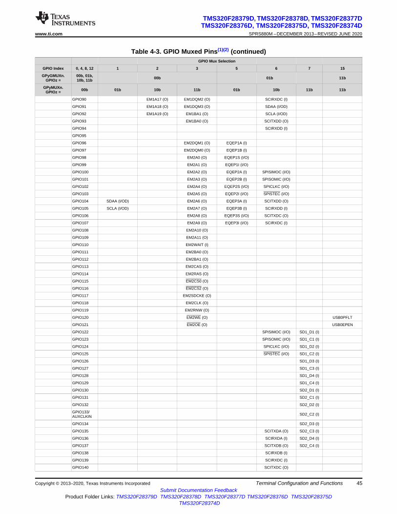
45
TMS320F28379D, TMS320F28378D, TMS320F28377DTMS320F28376D, TMS320F28375D, TMS320F28374D
www.ti.com SPRS880M –DECEMBER 2013–REVISED JUNE 2020
Submit Documentation FeedbackProduct Folder Links: TMS320F28379D TMS320F28378D TMS320F28377D TMS320F28376D TMS320F28375D
TMS320F28374D
Terminal Configuration and FunctionsCopyright © 2013–2020, Texas Instruments Incorporated
Table 4-3. GPIO Muxed Pins(1)(2) (continued)GPIO Mux Selection
GPIO Index 0, 4, 8, 12 1 2 3 5 6 7 15
GPyGMUXn.GPIOz =
00b, 01b,10b, 11b 00b 01b 11b
GPyMUXn.GPIOz = 00b 01b 10b 11b 01b 10b 11b 11b
GPIO90 EM1A17 (O) EM1DQM2 (O) SCIRXDC (I)
GPIO91 EM1A18 (O) EM1DQM3 (O) SDAA (I/OD)
GPIO92 EM1A19 (O) EM1BA1 (O) SCLA (I/OD)
GPIO93 EM1BA0 (O) SCITXDD (O)
GPIO94 SCIRXDD (I)
GPIO95
GPIO96 EM2DQM1 (O) EQEP1A (I)
GPIO97 EM2DQM0 (O) EQEP1B (I)
GPIO98 EM2A0 (O) EQEP1S (I/O)
GPIO99 EM2A1 (O) EQEP1I (I/O)
GPIO100 EM2A2 (O) EQEP2A (I) SPISIMOC (I/O)
GPIO101 EM2A3 (O) EQEP2B (I) SPISOMIC (I/O)
GPIO102 EM2A4 (O) EQEP2S (I/O) SPICLKC (I/O)
GPIO103 EM2A5 (O) EQEP2I (I/O) SPISTEC (I/O)
GPIO104 SDAA (I/OD) EM2A6 (O) EQEP3A (I) SCITXDD (O)
GPIO105 SCLA (I/OD) EM2A7 (O) EQEP3B (I) SCIRXDD (I)
GPIO106 EM2A8 (O) EQEP3S (I/O) SCITXDC (O)
GPIO107 EM2A9 (O) EQEP3I (I/O) SCIRXDC (I)
GPIO108 EM2A10 (O)
GPIO109 EM2A11 (O)
GPIO110 EM2WAIT (I)
GPIO111 EM2BA0 (O)
GPIO112 EM2BA1 (O)
GPIO113 EM2CAS (O)
GPIO114 EM2RAS (O)
GPIO115 EM2CS0 (O)
GPIO116 EM2CS2 (O)
GPIO117 EM2SDCKE (O)
GPIO118 EM2CLK (O)
GPIO119 EM2RNW (O)
GPIO120 EM2WE (O) USB0PFLT
GPIO121 EM2OE (O) USB0EPEN
GPIO122 SPISIMOC (I/O) SD1_D1 (I)
GPIO123 SPISOMIC (I/O) SD1_C1 (I)
GPIO124 SPICLKC (I/O) SD1_D2 (I)
GPIO125 SPISTEC (I/O) SD1_C2 (I)
GPIO126 SD1_D3 (I)
GPIO127 SD1_C3 (I)
GPIO128 SD1_D4 (I)
GPIO129 SD1_C4 (I)
GPIO130 SD2_D1 (I)
GPIO131 SD2_C1 (I)
GPIO132 SD2_D2 (I)
GPIO133/AUXCLKIN SD2_C2 (I)
GPIO134 SD2_D3 (I)
GPIO135 SCITXDA (O) SD2_C3 (I)
GPIO136 SCIRXDA (I) SD2_D4 (I)
GPIO137 SCITXDB (O) SD2_C4 (I)
GPIO138 SCIRXDB (I)
GPIO139 SCIRXDC (I)
GPIO140 SCITXDC (O)
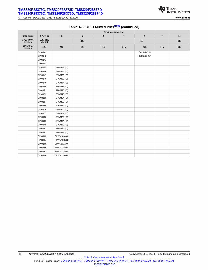
46
TMS320F28379D, TMS320F28378D, TMS320F28377DTMS320F28376D, TMS320F28375D, TMS320F28374DSPRS880M –DECEMBER 2013–REVISED JUNE 2020 www.ti.com
Submit Documentation FeedbackProduct Folder Links: TMS320F28379D TMS320F28378D TMS320F28377D TMS320F28376D TMS320F28375D
TMS320F28374D
Terminal Configuration and Functions Copyright © 2013–2020, Texas Instruments Incorporated
Table 4-3. GPIO Muxed Pins(1)(2) (continued)GPIO Mux Selection
GPIO Index 0, 4, 8, 12 1 2 3 5 6 7 15
GPyGMUXn.GPIOz =
00b, 01b,10b, 11b 00b 01b 11b
GPyMUXn.GPIOz = 00b 01b 10b 11b 01b 10b 11b 11b
GPIO141 SCIRXDD (I)
GPIO142 SCITXDD (O)
GPIO143
GPIO144
GPIO145 EPWM1A (O)
GPIO146 EPWM1B (O)
GPIO147 EPWM2A (O)
GPIO148 EPWM2B (O)
GPIO149 EPWM3A (O)
GPIO150 EPWM3B (O)
GPIO151 EPWM4A (O)
GPIO152 EPWM4B (O)
GPIO153 EPWM5A (O)
GPIO154 EPWM5B (O)
GPIO155 EPWM6A (O)
GPIO156 EPWM6B (O)
GPIO157 EPWM7A (O)
GPIO158 EPWM7B (O)
GPIO159 EPWM8A (O)
GPIO160 EPWM8B (O)
GPIO161 EPWM9A (O)
GPIO162 EPWM9B (O)
GPIO163 EPWM10A (O)
GPIO164 EPWM10B (O)
GPIO165 EPWM11A (O)
GPIO166 EPWM11B (O)
GPIO167 EPWM12A (O)
GPIO168 EPWM12B (O)
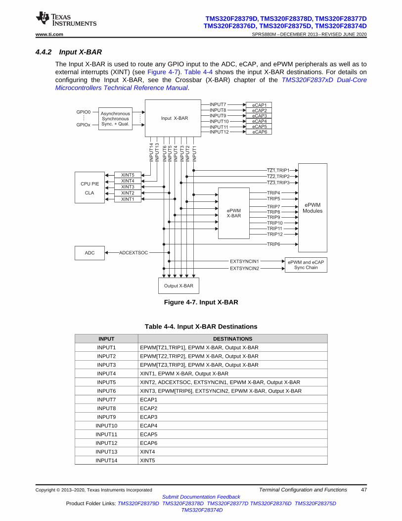
Input X-BAR
CPU PIE
CLA
GPIO0
GPIOx
EXTSYNCIN1
EXTSYNCIN2
eCAP1INPUT7
eCAP2eCAP3eCAP4eCAP5eCAP6
TRIP4
TRIP5
TRIP7TRIP8TRIP9
TRIP10
TRIP11
TRIP12
XINT5
XINT2
XINT1
XINT3
XINT4
ePWM and eCAPSync Chain
AsynchronousSynchronousSync. + Qual.
ADCEXTSOCADC
TZ1,TRIP1
TZ2 TRIP2,
TZ3 TRIP3,
TRIP6
INPUT8
INPUT9
INPUT10
INPUT11INPUT12
Output X-BAR
ePWMModules
INP
UT
4
INP
UT
13
INP
UT
14
INP
UT
6IN
PU
T5
INP
UT
3
INP
UT
2
INP
UT
1
ePWMX-BAR
47
TMS320F28379D, TMS320F28378D, TMS320F28377DTMS320F28376D, TMS320F28375D, TMS320F28374D
www.ti.com SPRS880M –DECEMBER 2013–REVISED JUNE 2020
Submit Documentation FeedbackProduct Folder Links: TMS320F28379D TMS320F28378D TMS320F28377D TMS320F28376D TMS320F28375D
TMS320F28374D
Terminal Configuration and FunctionsCopyright © 2013–2020, Texas Instruments Incorporated
4.4.2 Input X-BARThe Input X-BAR is used to route any GPIO input to the ADC, eCAP, and ePWM peripherals as well as toexternal interrupts (XINT) (see Figure 4-7). Table 4-4 shows the input X-BAR destinations. For details onconfiguring the Input X-BAR, see the Crossbar (X-BAR) chapter of the TMS320F2837xD Dual-CoreMicrocontrollers Technical Reference Manual.
Figure 4-7. Input X-BAR
Table 4-4. Input X-BAR Destinations
INPUT DESTINATIONSINPUT1 EPWM[TZ1,TRIP1], EPWM X-BAR, Output X-BARINPUT2 EPWM[TZ2,TRIP2], EPWM X-BAR, Output X-BARINPUT3 EPWM[TZ3,TRIP3], EPWM X-BAR, Output X-BARINPUT4 XINT1, EPWM X-BAR, Output X-BARINPUT5 XINT2, ADCEXTSOC, EXTSYNCIN1, EPWM X-BAR, Output X-BARINPUT6 XINT3, EPWM[TRIP6], EXTSYNCIN2, EPWM X-BAR, Output X-BARINPUT7 ECAP1INPUT8 ECAP2INPUT9 ECAP3INPUT10 ECAP4INPUT11 ECAP5INPUT12 ECAP6INPUT13 XINT4INPUT14 XINT5
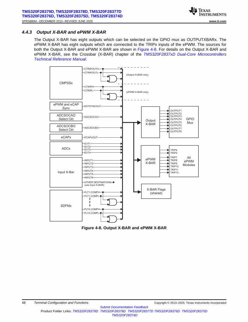
CMPSSx
ePWM and eCAPSync
ADCSOCAOSelect Ckt
ADCSOCBOSelect Ckt
eCAPx
ADCx
Input X-Bar
CTRIPOUTH
CTRIPOUTL
CTRIPH
CTRIPL
EXTSYNCOUT
ADCSOCAO
ADCSOCBO
ECAPxOUT
EVT1
INPUT1
INPUT2
INPUT3
INPUT4
INPUT5
INPUT6
FLT1.COMPH
FLT1.COMPL
FLT4.COMPH
FLT4.COMPL
GPIOMux
OUTPUT1
OUTPUT2OUTPUT3
OUTPUT4
OUTPUT5
OUTPUT6
OUTPUT7
OUTPUT8
OutputX-BAR
X-BAR Flags(shared)
AllePWM
Modules
TRIP4
TRIP5
TRIP7
TRIP8
TRIP9
TRIP10
TRIP11
TRIP12
ePWMX-BAR
SDFMx
(Output X-BAR only)
(ePWM X-BAR only)
EVT2EVT3
EVT4
OTHER DESTINATIONS(see Input X-BAR)
48
TMS320F28379D, TMS320F28378D, TMS320F28377DTMS320F28376D, TMS320F28375D, TMS320F28374DSPRS880M –DECEMBER 2013–REVISED JUNE 2020 www.ti.com
Submit Documentation FeedbackProduct Folder Links: TMS320F28379D TMS320F28378D TMS320F28377D TMS320F28376D TMS320F28375D
TMS320F28374D
Terminal Configuration and Functions Copyright © 2013–2020, Texas Instruments Incorporated
4.4.3 Output X-BAR and ePWM X-BARThe Output X-BAR has eight outputs which can be selected on the GPIO mux as OUTPUTXBARx. TheePWM X-BAR has eight outputs which are connected to the TRIPx inputs of the ePWM. The sources forboth the Output X-BAR and ePWM X-BAR are shown in Figure 4-8. For details on the Output X-BAR andePWM X-BAR, see the Crossbar (X-BAR) chapter of the TMS320F2837xD Dual-Core MicrocontrollersTechnical Reference Manual.
Figure 4-8. Output X-BAR and ePWM X-BAR

49
TMS320F28379D, TMS320F28378D, TMS320F28377DTMS320F28376D, TMS320F28375D, TMS320F28374D
www.ti.com SPRS880M –DECEMBER 2013–REVISED JUNE 2020
Submit Documentation FeedbackProduct Folder Links: TMS320F28379D TMS320F28378D TMS320F28377D TMS320F28376D TMS320F28375D
TMS320F28374D
Terminal Configuration and FunctionsCopyright © 2013–2020, Texas Instruments Incorporated
4.4.4 USB Pin MuxingTable 4-5 shows assignment of the alternate USB function mapping. These can be configured with theGPBAMSEL register.
Table 4-5. Alternate USB Function
GPIO GPBAMSEL SETTING USB FUNCTIONGPIO42 GPBAMSEL[10] = 1b USB0DMGPIO43 GPBAMSEL[11] = 1b USB0DP
4.4.5 High-Speed SPI Pin MuxingThe SPI module on this device has a high-speed mode. To achieve the highest possible speed, a specialGPIO configuration is used on a single GPIO mux option for each SPI. These GPIOs may also be used bythe SPI when not in high-speed mode (HS_MODE = 0).
To select the mux options that enable the SPI high-speed mode, configure the GPyGMUX and GPyMUXregisters as shown in Table 4-6.
Table 4-6. GPIO Configuration for High-Speed SPI
GPIO SPI SIGNAL MUX CONFIGURATIONSPIA
GPIO58 SPISIMOA GPBGMUX2[21:20]=11b GPBMUX2[21:20]=11bGPIO59 SPISOMIA GPBGMUX2[23:22]=11b GPBMUX2[23:22]=11bGPIO60 SPICLKA GPBGMUX2[25:24]=11b GPBMUX2[25:24]=11bGPIO61 SPISTEA GPBGMUX2[27:26]=11b GPBMUX2[27:26]=11b
SPIBGPIO63 SPISIMOB GPBGMUX2[31:30]=11b GPBMUX2[31:30]=11bGPIO64 SPISOMIB GPCGMUX1[1:0]=11b GPCMUX1[1:0]=11bGPIO65 SPICLKB GPCGMUX1[3:2]=11b GPCMUX1[3:2]=11bGPIO66 SPISTEB GPCGMUX1[5:4]=11b GPCMUX1[5:4]=11b
SPICGPIO69 SPISIMOC GPCGMUX1[11:10]=11b GPCMUX1[11:10]=11bGPIO70 SPISOMIC GPCGMUX1[13:12]=11b GPCMUX1[13:12]=11bGPIO71 SPICLKC GPCGMUX1[15:14]=11b GPCMUX1[15:14]=11bGPIO72 SPISTEC GPCGMUX1[17:16]=11b GPCMUX1[17:16]=11b
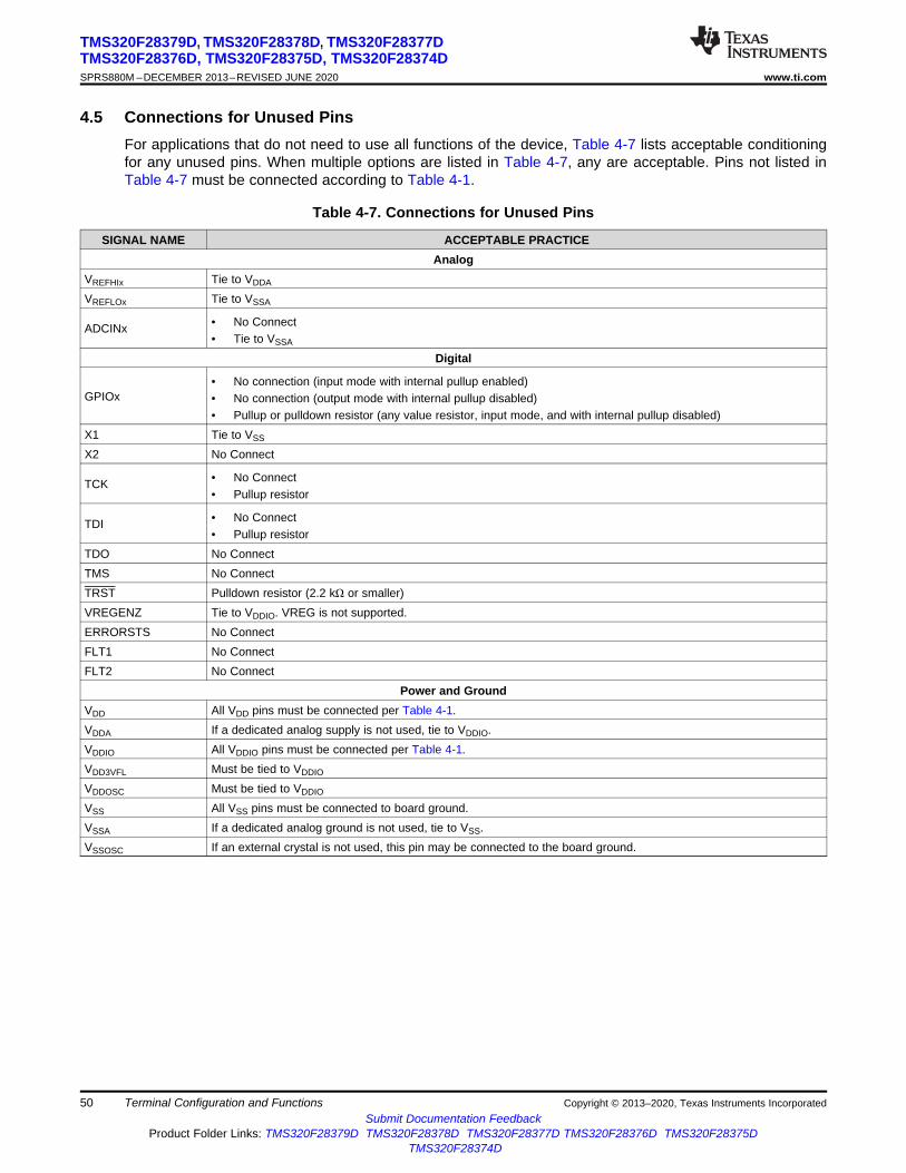
50
TMS320F28379D, TMS320F28378D, TMS320F28377DTMS320F28376D, TMS320F28375D, TMS320F28374DSPRS880M –DECEMBER 2013–REVISED JUNE 2020 www.ti.com
Submit Documentation FeedbackProduct Folder Links: TMS320F28379D TMS320F28378D TMS320F28377D TMS320F28376D TMS320F28375D
TMS320F28374D
Terminal Configuration and Functions Copyright © 2013–2020, Texas Instruments Incorporated
4.5 Connections for Unused PinsFor applications that do not need to use all functions of the device, Table 4-7 lists acceptable conditioningfor any unused pins. When multiple options are listed in Table 4-7, any are acceptable. Pins not listed inTable 4-7 must be connected according to Table 4-1.
Table 4-7. Connections for Unused Pins
SIGNAL NAME ACCEPTABLE PRACTICEAnalog
VREFHIx Tie to VDDA
VREFLOx Tie to VSSA
ADCINx • No Connect• Tie to VSSA
Digital
GPIOx• No connection (input mode with internal pullup enabled)• No connection (output mode with internal pullup disabled)• Pullup or pulldown resistor (any value resistor, input mode, and with internal pullup disabled)
X1 Tie to VSS
X2 No Connect
TCK • No Connect• Pullup resistor
TDI • No Connect• Pullup resistor
TDO No ConnectTMS No ConnectTRST Pulldown resistor (2.2 kΩ or smaller)VREGENZ Tie to VDDIO. VREG is not supported.ERRORSTS No ConnectFLT1 No ConnectFLT2 No Connect
Power and GroundVDD All VDD pins must be connected per Table 4-1.VDDA If a dedicated analog supply is not used, tie to VDDIO.VDDIO All VDDIO pins must be connected per Table 4-1.VDD3VFL Must be tied to VDDIO
VDDOSC Must be tied to VDDIO
VSS All VSS pins must be connected to board ground.VSSA If a dedicated analog ground is not used, tie to VSS.VSSOSC If an external crystal is not used, this pin may be connected to the board ground.

51
TMS320F28379D, TMS320F28378D, TMS320F28377DTMS320F28376D, TMS320F28375D, TMS320F28374D
www.ti.com SPRS880M –DECEMBER 2013–REVISED JUNE 2020
Submit Documentation FeedbackProduct Folder Links: TMS320F28379D TMS320F28378D TMS320F28377D TMS320F28376D TMS320F28375D
TMS320F28374D
SpecificationsCopyright © 2013–2020, Texas Instruments Incorporated
(1) Stresses beyond those listed under absolute maximum ratings may cause permanent damage to the device. These are stress ratingsonly, and functional operation of the device at these or any other conditions beyond those indicated under Section 5.4 is not implied.Exposure to absolute-maximum-rated conditions for extended periods may affect device reliability.
(2) All voltage values are with respect to VSS, unless otherwise noted.(3) Continuous clamp current per pin is ±2 mA. Do not operate in this condition continuously as VDDIO/VDDA voltage may internally rise and
impact other electrical specifications.(4) Long-term high-temperature storage or extended use at maximum temperature conditions may result in a reduction of overall device life.
For additional information, see Semiconductor and IC Package Thermal Metrics.
5 Specifications
5.1 Absolute Maximum Ratings (1) (2)
over operating free-air temperature range (unless otherwise noted)MIN MAX UNIT
Supply voltage
VDDIO with respect to VSS –0.3 4.6
VVDD3VFL with respect to VSS –0.3 4.6VDDOSC with respect to VSS –0.3 4.6VDD with respect to VSS –0.3 1.5
Analog voltage VDDA with respect to VSSA –0.3 4.6 VInput voltage VIN (3.3 V) –0.3 4.6 VOutput voltage VO –0.3 4.6 V
Input clamp current
Digital/analog input (per pin), IIK(VIN < VSS/VSSA or VIN > VDDIO/VDDA) (3) –20 20
mATotal for all inputs, IIKTOTAL(VIN < VSS/VSSA or VIN > VDDIO/VDDA) –20 20
Output current Digital output (per pin), IOUT –20 20 mAFree-Air temperature TA –40 125 °COperating junction temperature TJ –40 150 °CStorage temperature (4) Tstg –65 150 °C

52
TMS320F28379D, TMS320F28378D, TMS320F28377DTMS320F28376D, TMS320F28375D, TMS320F28374DSPRS880M –DECEMBER 2013–REVISED JUNE 2020 www.ti.com
Submit Documentation FeedbackProduct Folder Links: TMS320F28379D TMS320F28378D TMS320F28377D TMS320F28376D TMS320F28375D
TMS320F28374D
Specifications Copyright © 2013–2020, Texas Instruments Incorporated
(1) JEDEC document JEP155 states that 500-V HBM allows safe manufacturing with a standard ESD control process.(2) JEDEC document JEP157 states that 250-V CDM allows safe manufacturing with a standard ESD control process.
5.2 ESD Ratings – CommercialVALUE UNIT
TMS320F28379D, TMS320F28376D, TMS320F28375D, and TMS320F23874D in 337-ball ZWT package
V(ESD) Electrostatic discharge (ESD)Human-body model (HBM), per ANSI/ESDA/JEDEC JS-001 (1) ±2000
VCharged-device model (CDM), per JEDEC specification JESD22-C101 or ANSI/ESDA/JEDEC JS-002 (2)
±500
TMS320F28379D, TMS320F28378D, TMS320F28376D, TMS320F28375D, and TMS320F23874D in 176-pin PTP package
V(ESD) Electrostatic discharge (ESD)Human-body model (HBM), per ANSI/ESDA/JEDEC JS-001 (1) ±2000
VCharged-device model (CDM), per JEDEC specification JESD22-C101 or ANSI/ESDA/JEDEC JS-002 (2)
±500
TMS320F23875D in 100-pin PZP package
V(ESD) Electrostatic discharge (ESD)Human-body model (HBM), per ANSI/ESDA/JEDEC JS-001 (1) ±2000
VCharged-device model (CDM), per JEDEC specification JESD22-C101 or ANSI/ESDA/JEDEC JS-002 (2)
±500
(1) AEC Q100-002 indicates HBM stressing is done in accordance with the ANSI/ESDA/JEDEC JS-001 specification.
5.3 ESD Ratings – AutomotiveVALUE UNIT
TMS320F28377D in 337-ball ZWT package
V(ESD) Electrostatic discharge
Human body model (HBM), perAEC Q100-002 (1)
All pins ±2000
VCharged device model (CDM),per AEC Q100-011
All pins ±500Corner balls on 337-ball ZWT:A1, A19, W1, W19
±750
TMS320F28377D in 176-pin PTP package
V(ESD) Electrostatic discharge
Human body model (HBM), perAEC Q100-002 (1)
All pins ±2000
VCharged device model (CDM),per AEC Q100-011
All pins ±500Corner pins on 176-pin PTP:1, 44, 45, 88, 89, 132, 133, 176
±750
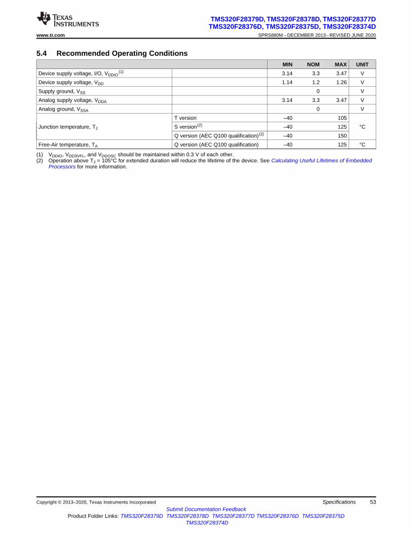
53
TMS320F28379D, TMS320F28378D, TMS320F28377DTMS320F28376D, TMS320F28375D, TMS320F28374D
www.ti.com SPRS880M –DECEMBER 2013–REVISED JUNE 2020
Submit Documentation FeedbackProduct Folder Links: TMS320F28379D TMS320F28378D TMS320F28377D TMS320F28376D TMS320F28375D
TMS320F28374D
SpecificationsCopyright © 2013–2020, Texas Instruments Incorporated
(1) VDDIO, VDD3VFL, and VDDOSC should be maintained within 0.3 V of each other.(2) Operation above TJ = 105°C for extended duration will reduce the lifetime of the device. See Calculating Useful Lifetimes of Embedded
Processors for more information.
5.4 Recommended Operating ConditionsMIN NOM MAX UNIT
Device supply voltage, I/O, VDDIO(1) 3.14 3.3 3.47 V
Device supply voltage, VDD 1.14 1.2 1.26 VSupply ground, VSS 0 VAnalog supply voltage, VDDA 3.14 3.3 3.47 VAnalog ground, VSSA 0 V
Junction temperature, TJ
T version –40 105°CS version (2) –40 125
Q version (AEC Q100 qualification) (2) –40 150Free-Air temperature, TA Q version (AEC Q100 qualification) –40 125 °C

54
TMS320F28379D, TMS320F28378D, TMS320F28377DTMS320F28376D, TMS320F28375D, TMS320F28374DSPRS880M –DECEMBER 2013–REVISED JUNE 2020 www.ti.com
Submit Documentation FeedbackProduct Folder Links: TMS320F28379D TMS320F28378D TMS320F28377D TMS320F28376D TMS320F28375D
TMS320F28374D
Specifications Copyright © 2013–2020, Texas Instruments Incorporated
5.5 Power Consumption SummaryCurrent values listed in this section are representative for the test conditions given and not the absolutemaximum possible. The actual device currents in an application will vary with application code and pinconfigurations. Table 5-1 shows the device current consumption at 200-MHz SYSCLK.
(1) IDDIO current is dependent on the electrical loading on the I/O pins.(2) TYP: Vnom, 30°C(3) MAX: Vmax, 125°C(4) The following is executed in a loop on CPU1:
• All of the communication peripherals are exercised in loop-back mode: CAN-A to CAN-B; SPI-A to SPI-C; SCI-A to SCI-D; I2C-A toI2C-B; McBSP-A to McBSP-B; USB
• SDFM1 to SDFM4 active• ePWM1 to ePWM12 generate 400-kHz PWM output on 24 pins• CPU TIMERs active• DMA does 32-bit burst transfers• CLA1 does multiply-accumulate tasks• All ADCs perform continuous conversion• All DACs ramp voltage up/down at 150 kHz• CMPSS1 to CMPSS8 activeThe following is executed in a loop on CPU2:• CPU TIMERs active• CLA1 does multiply-accumulate tasks• VCU does complex multiply/accumulate with parallel load• TMU calculates a cosine• FPU does multiply/accumulate with parallel load
(5) CPU2 must go into IDLE mode before CPU1 enters HALT mode.(6) CPU2 must go into reset/IDLE/STANDBY mode before CPU1 enters HIBERNATE mode.(7) Brownout events during flash programming can corrupt flash data. Programming environments using alternate power sources (such as a
USB programmer) must be capable of supplying the rated current for the device and other system components with sufficient margin toavoid supply brownout conditions.
Table 5-1. Device Current Consumption at 200-MHz SYSCLK
MODE TEST CONDITIONSIDD IDDIO
(1) IDDA IDD3VFL
TYP (2) MAX (3) TYP (2) MAX (3) TYP (2) MAX (3) TYP (2) MAX (3)
Operational
• Code is running out of RAM. (4)
• All I/O pins are left unconnected.• Peripherals not active have their
clocks disabled.• FLASH is read and in active state.• XCLKOUT is enabled at SYSCLK/4.
325 mA 495 mA 30 mA 13 mA 20 mA 33 mA 40 mA
IDLE
• Both CPU1 and CPU2 are in IDLEmode.
• Flash is powered down.• XCLKOUT is turned off.
105 mA 250 mA 3 mA 10 mA 10 µA 150 µA 10 µA 150 µA
STANDBY
• Both CPU1 and CPU2 are inSTANDBY mode.
• Flash is powered down.• XCLKOUT is turned off.
30 mA 170 mA 3 mA 10 mA 5 µA 150 µA 10 µA 150 µA
HALT (5)• CPU1 watchdog is running.• Flash is powered down.• XCLKOUT is turned off.
1.5 mA 120 mA 750 µA 2 mA 5 µA 150 µA 10 µA 150 µA
HIBERNATE (6)
• CPU1.M0 and CPU1.M1 RAMs are inlow-power data retention mode.
• CPU2.M0 and CPU2.M1 RAMs are inlow-power data retention mode.
300 µA 5 mA 750 µA 2 mA 5 µA 75 µA 1 µA 50 µA
FlashErase/Program (7)
• CPU1 is running from RAM.• CPU2 is running from Flash.• All I/O pins are left unconnected.• Peripheral clocks are disabled.• CPU1 is performing Flash Erase and
Programming.• CPU2 is accessing Flash locations to
keep bank active.• XCLKOUT is turned off.
242 mA 360 mA 3 mA 10 mA 10 µA 150 µA 53 mA 65 mA
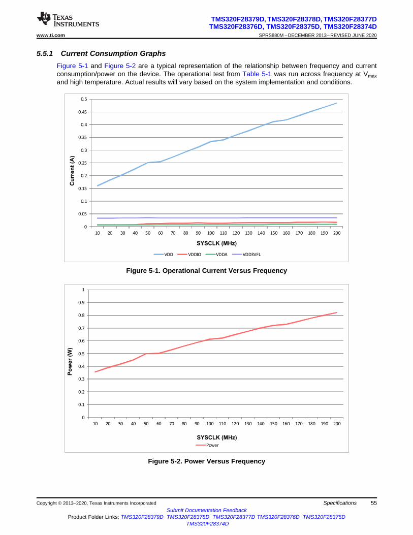
0
0.1
0.2
0.3
0.4
0.5
0.6
0.7
0.8
0.9
1
10 20 30 40 50 60 70 80 90 100 110 120 130 140 150 160 170 180 190 200
Power
Po
we
r (W
)
SYSCLK (MHz)
0
0.05
0.1
0.15
0.2
0.25
0.3
0.35
0.4
0.45
0.5
10 20 30 40 50 60 70 80 90 100 110 120 130 140 150 160 170 180 190 200
VDD VDDIO VDDA VDD3VFL
SYSCLK (MHz)
Cu
rre
nt
(A)
55
TMS320F28379D, TMS320F28378D, TMS320F28377DTMS320F28376D, TMS320F28375D, TMS320F28374D
www.ti.com SPRS880M –DECEMBER 2013–REVISED JUNE 2020
Submit Documentation FeedbackProduct Folder Links: TMS320F28379D TMS320F28378D TMS320F28377D TMS320F28376D TMS320F28375D
TMS320F28374D
SpecificationsCopyright © 2013–2020, Texas Instruments Incorporated
5.5.1 Current Consumption GraphsFigure 5-1 and Figure 5-2 are a typical representation of the relationship between frequency and currentconsumption/power on the device. The operational test from Table 5-1 was run across frequency at Vmaxand high temperature. Actual results will vary based on the system implementation and conditions.
Figure 5-1. Operational Current Versus Frequency
Figure 5-2. Power Versus Frequency
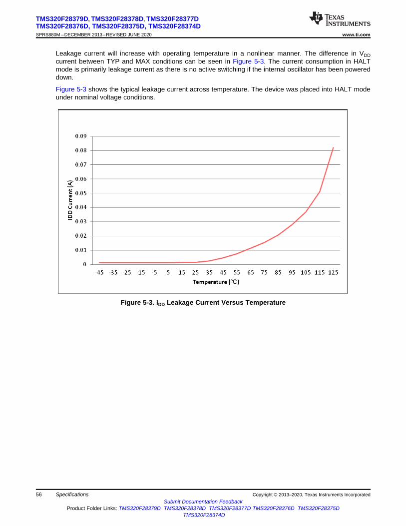
56
TMS320F28379D, TMS320F28378D, TMS320F28377DTMS320F28376D, TMS320F28375D, TMS320F28374DSPRS880M –DECEMBER 2013–REVISED JUNE 2020 www.ti.com
Submit Documentation FeedbackProduct Folder Links: TMS320F28379D TMS320F28378D TMS320F28377D TMS320F28376D TMS320F28375D
TMS320F28374D
Specifications Copyright © 2013–2020, Texas Instruments Incorporated
Leakage current will increase with operating temperature in a nonlinear manner. The difference in VDDcurrent between TYP and MAX conditions can be seen in Figure 5-3. The current consumption in HALTmode is primarily leakage current as there is no active switching if the internal oscillator has been powereddown.
Figure 5-3 shows the typical leakage current across temperature. The device was placed into HALT modeunder nominal voltage conditions.
Figure 5-3. IDD Leakage Current Versus Temperature
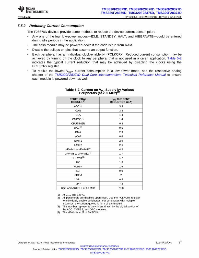
57
TMS320F28379D, TMS320F28378D, TMS320F28377DTMS320F28376D, TMS320F28375D, TMS320F28374D
www.ti.com SPRS880M –DECEMBER 2013–REVISED JUNE 2020
Submit Documentation FeedbackProduct Folder Links: TMS320F28379D TMS320F28378D TMS320F28377D TMS320F28376D TMS320F28375D
TMS320F28374D
SpecificationsCopyright © 2013–2020, Texas Instruments Incorporated
5.5.2 Reducing Current ConsumptionThe F2837xD devices provide some methods to reduce the device current consumption:• Any one of the four low-power modes—IDLE, STANDBY, HALT, and HIBERNATE—could be entered
during idle periods in the application.• The flash module may be powered down if the code is run from RAM.• Disable the pullups on pins that assume an output function.• Each peripheral has an individual clock-enable bit (PCLKCRx). Reduced current consumption may be
achieved by turning off the clock to any peripheral that is not used in a given application. Table 5-2indicates the typical current reduction that may be achieved by disabling the clocks using thePCLKCRx register.
• To realize the lowest VDDA current consumption in a low-power mode, see the respective analogchapter of the TMS320F2837xD Dual-Core Microcontrollers Technical Reference Manual to ensureeach module is powered down as well.
(1) At Vmax and 125°C.(2) All peripherals are disabled upon reset. Use the PCLKCRx register
to individually enable peripherals. For peripherals with multipleinstances, the current quoted is for a single module.
(3) This number represents the current drawn by the digital portion ofthe ADC, CMPSS, and DAC modules.
(4) The ePWM is at /2 of SYSCLK.
Table 5-2. Current on VDD Supply by VariousPeripherals (at 200 MHz) (1)
PERIPHERALMODULE (2)
IDD CURRENTREDUCTION (mA)
ADC (3) 3.3CAN 3.3CLA 1.4
CMPSS (3) 1.4CPUTIMER 0.3
DAC (3) 0.6DMA 2.9eCAP 0.6EMIF1 2.9EMIF2 2.6
ePWM1 to ePWM4 (4) 4.5ePWM5 to ePWM12 (4) 1.7
HRPWM (4) 1.7I2C 1.3
McBSP 1.6SCI 0.9
SDFM 2SPI 0.5uPP 7.3
USB and AUXPLL at 60 MHz 23.8
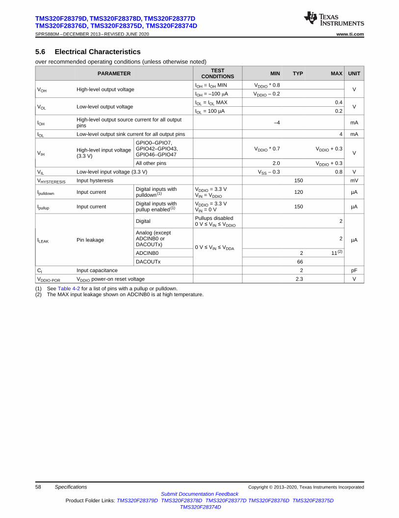
58
TMS320F28379D, TMS320F28378D, TMS320F28377DTMS320F28376D, TMS320F28375D, TMS320F28374DSPRS880M –DECEMBER 2013–REVISED JUNE 2020 www.ti.com
Submit Documentation FeedbackProduct Folder Links: TMS320F28379D TMS320F28378D TMS320F28377D TMS320F28376D TMS320F28375D
TMS320F28374D
Specifications Copyright © 2013–2020, Texas Instruments Incorporated
(1) See Table 4-2 for a list of pins with a pullup or pulldown.(2) The MAX input leakage shown on ADCINB0 is at high temperature.
5.6 Electrical Characteristicsover recommended operating conditions (unless otherwise noted)
PARAMETER TESTCONDITIONS MIN TYP MAX UNIT
VOH High-level output voltageIOH = IOH MIN VDDIO * 0.8
VIOH = –100 μA VDDIO – 0.2
VOL Low-level output voltageIOL = IOL MAX 0.4
VIOL = 100 µA 0.2
IOHHigh-level output source current for all outputpins –4 mA
IOL Low-level output sink current for all output pins 4 mA
VIHHigh-level input voltage(3.3 V)
GPIO0–GPIO7,GPIO42–GPIO43,GPIO46–GPIO47
VDDIO * 0.7 VDDIO + 0.3V
All other pins 2.0 VDDIO + 0.3VIL Low-level input voltage (3.3 V) VSS – 0.3 0.8 VVHYSTERESIS Input hysteresis 150 mV
Ipulldown Input current Digital inputs withpulldown (1)
VDDIO = 3.3 VVIN = VDDIO
120 µA
Ipullup Input current Digital inputs withpullup enabled (1)
VDDIO = 3.3 VVIN = 0 V 150 µA
ILEAK Pin leakage
Digital Pullups disabled0 V ≤ VIN ≤ VDDIO
2
µAAnalog (exceptADCINB0 orDACOUTx) 0 V ≤ VIN ≤ VDDA
2
ADCINB0 2 11 (2)
DACOUTx 66CI Input capacitance 2 pFVDDIO-POR VDDIO power-on reset voltage 2.3 V

59
TMS320F28379D, TMS320F28378D, TMS320F28377DTMS320F28376D, TMS320F28375D, TMS320F28374D
www.ti.com SPRS880M –DECEMBER 2013–REVISED JUNE 2020
Submit Documentation FeedbackProduct Folder Links: TMS320F28379D TMS320F28378D TMS320F28377D TMS320F28376D TMS320F28375D
TMS320F28374D
SpecificationsCopyright © 2013–2020, Texas Instruments Incorporated
(1) These values are based on a JEDEC-defined 2S2P system (with the exception of the Theta JC [RΘJC] value, which is based on aJEDEC-defined 1S0P system) and will change based on environment as well as application. For more information, see theseEIA/JEDEC standards:• JESD51-2, Integrated Circuits Thermal Test Method Environmental Conditions - Natural Convection (Still Air)• JESD51-3, Low Effective Thermal Conductivity Test Board for Leaded Surface Mount Packages• JESD51-7, High Effective Thermal Conductivity Test Board for Leaded Surface Mount Packages• JESD51-9, Test Boards for Area Array Surface Mount Package Thermal Measurements
(2) lfm = linear feet per minute
5.7 Thermal Resistance Characteristics
5.7.1 ZWT Package°C/W (1) AIR FLOW (lfm) (2)
RΘJC Junction-to-case thermal resistance 8.3 N/ARΘJB Junction-to-board thermal resistance 11.6 N/ARΘJA (High k PCB) Junction-to-free air thermal resistance 21.5 0
RΘJMA Junction-to-moving air thermal resistance19.0 15017.8 25016.5 500
PsiJT Junction-to-package top
0.2 00.3 1500.4 2500.5 500
PsiJB Junction-to-board
11.4 011.3 15011.2 25011.0 500
(1) These values are based on a JEDEC-defined 2S2P system (with the exception of the Theta JC [RΘJC] value, which is based on aJEDEC-defined 1S0P system) and will change based on environment as well as application. For more information, see theseEIA/JEDEC standards:• JESD51-2, Integrated Circuits Thermal Test Method Environmental Conditions - Natural Convection (Still Air)• JESD51-3, Low Effective Thermal Conductivity Test Board for Leaded Surface Mount Packages• JESD51-7, High Effective Thermal Conductivity Test Board for Leaded Surface Mount Packages• JESD51-9, Test Boards for Area Array Surface Mount Package Thermal Measurements
(2) lfm = linear feet per minute
5.7.2 PTP Package°C/W (1) AIR FLOW (lfm) (2)
RΘJC Junction-to-case thermal resistance 6.97 N/ARΘJB Junction-to-board thermal resistance 6.05 N/ARΘJA (High k PCB) Junction-to-free air thermal resistance 17.8 0
RΘJMA Junction-to-moving air thermal resistance12.8 15011.4 25010.1 500
PsiJT Junction-to-package top
0.11 00.24 1500.33 2500.42 500
PsiJB Junction-to-board
6.1 05.5 1505.4 2505.3 500
60
TMS320F28379D, TMS320F28378D, TMS320F28377DTMS320F28376D, TMS320F28375D, TMS320F28374DSPRS880M –DECEMBER 2013–REVISED JUNE 2020 www.ti.com
Submit Documentation FeedbackProduct Folder Links: TMS320F28379D TMS320F28378D TMS320F28377D TMS320F28376D TMS320F28375D
TMS320F28374D
Specifications Copyright © 2013–2020, Texas Instruments Incorporated
(1) These values are based on a JEDEC-defined 2S2P system (with the exception of the Theta JC [RΘJC] value, which is based on aJEDEC-defined 1S0P system) and will change based on environment as well as application. For more information, see theseEIA/JEDEC standards:• JESD51-2, Integrated Circuits Thermal Test Method Environmental Conditions - Natural Convection (Still Air)• JESD51-3, Low Effective Thermal Conductivity Test Board for Leaded Surface Mount Packages• JESD51-7, High Effective Thermal Conductivity Test Board for Leaded Surface Mount Packages• JESD51-9, Test Boards for Area Array Surface Mount Package Thermal Measurements
(2) lfm = linear feet per minute
5.7.3 PZP Package°C/W (1) AIR FLOW (lfm) (2)
RΘJC Junction-to-case thermal resistance 4.3 N/ARΘJB Junction-to-board thermal resistance 5.9 N/ARΘJA (High k PCB) Junction-to-free air thermal resistance 19.1 0
RΘJMA Junction-to-moving air thermal resistance14.3 15012.8 25011.4 500
PsiJT Junction-to-package top
0.03 00.09 1500.12 2500.20 500
PsiJB Junction-to-board
6.0 05.5 1505.5 2505.3 500
5.8 Thermal Design ConsiderationsBased on the end application design and operational profile, the IDD and IDDIO currents could vary.Systems that exceed the recommended maximum power dissipation in the end product may requireadditional thermal enhancements. Ambient temperature (TA) varies with the end application and productdesign. The critical factor that affects reliability and functionality is TJ, the junction temperature, not theambient temperature. Hence, care should be taken to keep TJ within the specified limits. Tcase should bemeasured to estimate the operating junction temperature TJ. Tcase is normally measured at the center ofthe package top-side surface. The thermal application report Semiconductor and IC Package ThermalMetrics helps to understand the thermal metrics and definitions.

61
TMS320F28379D, TMS320F28378D, TMS320F28377DTMS320F28376D, TMS320F28375D, TMS320F28374D
www.ti.com SPRS880M –DECEMBER 2013–REVISED JUNE 2020
Submit Documentation FeedbackProduct Folder Links: TMS320F28379D TMS320F28378D TMS320F28377D TMS320F28376D TMS320F28375D
TMS320F28374D
SpecificationsCopyright © 2013–2020, Texas Instruments Incorporated
5.9 System
5.9.1 Power Sequencing
5.9.1.1 Signal Pin Requirements
Before powering the device, no voltage larger than 0.3 V above VDDIO can be applied to any digital pin,and no voltage larger than 0.3 V above VDDA can be applied to any analog pin (including VREFHI).
5.9.1.2 VDDIO, VDDA, VDD3VFL, and VDDOSC Requirements
The 3.3-V supplies should be powered up together and kept within 0.3 V of each other during functionaloperation.
5.9.1.3 VDD Requirements
The internal VREG is not supported. The VREGENZ pin must be tied to VDDIO and an external sourceused to supply 1.2 V to VDD. During the ramp, VDD should be kept no more than 0.3 V above VDDIO.
VDDOSC and VDD must be powered on and off at the same time. VDDOSC should not be powered on whenVDD is off. For applications not powering VDDOSC and VDD at the same time, see the "INTOSC: VDDOSCPowered Without VDD Can Cause INTOSC Frequency Drift" advisory in the TMS320F2837xD Dual-CoreMCUs Silicon Errata.
There is an internal 12.8-mA current source from VDD3VFL to VDD when the flash banks are active. Whenthe flash banks are active and the device is in a low-activity state (for example, a low-power mode), thisinternal current source can cause VDD to rise to approximately 1.3 V. There will be zero current load to theexternal system VDD regulator while in this condition. This is not an issue for most regulators; however, ifthe system voltage regulator requires a minimum load for proper operation, then an external 82Ω resistorcan be added to the board to ensure a minimal current load on VDD. See the "Low-Power Modes: PowerDown Flash or Maintain Minimum Device Activity" advisory in the TMS320F2837xD Dual-Core MCUsSilicon Errata.
5.9.1.4 Supply Ramp Rate
The supplies should ramp to full rail within 10 ms. Table 5-3 shows the supply ramp rate.
Table 5-3. Supply Ramp RateMIN MAX UNIT
Supply ramp rate VDDIO, VDD, VDDA, VDD3VFL, VDDOSC with respect to VSS 330 105 V/s
5.9.1.5 Supply Supervision
An internal power-on-reset (POR) circuit keeps the I/Os in a high-impedance state during power up.External supply voltage supervisors (SVS) can be used to monitor the voltage on the 3.3-V and 1.2-V railsand drive XRS low when supplies are outside operational specifications.
NOTEIf the supply voltage is held near the POR threshold, then the device may drive periodicresets onto the XRS pin.
5.9.2 Reset TimingXRS is the device reset pin. It functions as an input and open-drain output. The device has a built-inpower-on reset (POR). During power up, the POR circuit drives the XRS pin low. A watchdog or NMIwatchdog reset also drives the pin low. An external circuit may drive the pin to assert a device reset.
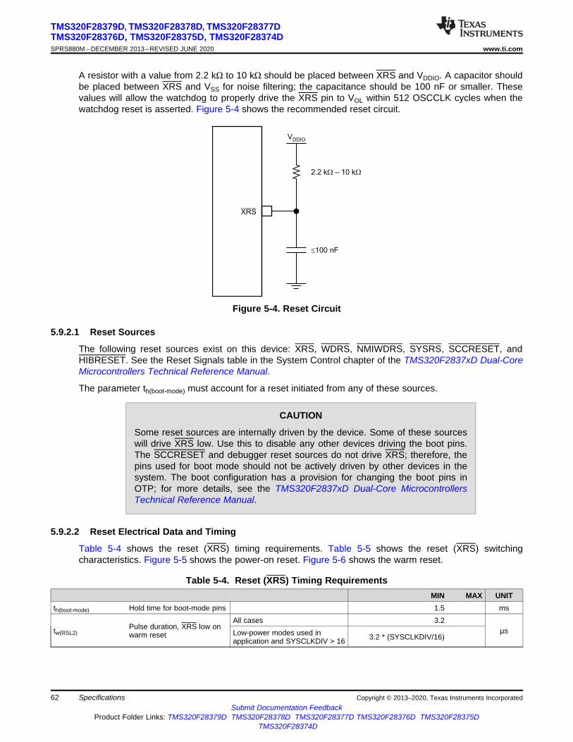
XRS
£100 nF
2.2 k – 10 kW W
VDDIO
62
TMS320F28379D, TMS320F28378D, TMS320F28377DTMS320F28376D, TMS320F28375D, TMS320F28374DSPRS880M –DECEMBER 2013–REVISED JUNE 2020 www.ti.com
Submit Documentation FeedbackProduct Folder Links: TMS320F28379D TMS320F28378D TMS320F28377D TMS320F28376D TMS320F28375D
TMS320F28374D
Specifications Copyright © 2013–2020, Texas Instruments Incorporated
A resistor with a value from 2.2 kΩ to 10 kΩ should be placed between XRS and VDDIO. A capacitor shouldbe placed between XRS and VSS for noise filtering; the capacitance should be 100 nF or smaller. Thesevalues will allow the watchdog to properly drive the XRS pin to VOL within 512 OSCCLK cycles when thewatchdog reset is asserted. Figure 5-4 shows the recommended reset circuit.
Figure 5-4. Reset Circuit
5.9.2.1 Reset Sources
The following reset sources exist on this device: XRS, WDRS, NMIWDRS, SYSRS, SCCRESET, andHIBRESET. See the Reset Signals table in the System Control chapter of the TMS320F2837xD Dual-CoreMicrocontrollers Technical Reference Manual.
The parameter th(boot-mode) must account for a reset initiated from any of these sources.
CAUTION
Some reset sources are internally driven by the device. Some of these sourceswill drive XRS low. Use this to disable any other devices driving the boot pins.The SCCRESET and debugger reset sources do not drive XRS; therefore, thepins used for boot mode should not be actively driven by other devices in thesystem. The boot configuration has a provision for changing the boot pins inOTP; for more details, see the TMS320F2837xD Dual-Core MicrocontrollersTechnical Reference Manual.
5.9.2.2 Reset Electrical Data and Timing
Table 5-4 shows the reset (XRS) timing requirements. Table 5-5 shows the reset (XRS) switchingcharacteristics. Figure 5-5 shows the power-on reset. Figure 5-6 shows the warm reset.
Table 5-4. Reset (XRS) Timing RequirementsMIN MAX UNIT
th(boot-mode) Hold time for boot-mode pins 1.5 ms
tw(RSL2)Pulse duration, XRS low onwarm reset
All cases 3.2µsLow-power modes used in
application and SYSCLKDIV > 16 3.2 * (SYSCLKDIV/16)

th(boot-mode)(A)
XRS
Boot-Mode
Pins
I/O Pins
CPUExecution
Phase
Boot-ROM execution starts(initiated by any reset source)
User-Code Execution Starts
User Code
Boot ROM
User-Code Dependent
User Code
Peripheral/GPIO Function
User-Code Dependent
GPIO Pins as Input (Pullups are Disabled)
GPIO Pins as Input Peripheral/GPIO Function
tw(RSL2)
th(boot-mode)(B)
XRS(A)
Boot-Mode
Pins
V V
(3.3 V)DDIO DDA,
V (1.2 V)DD
User-code dependent
Boot-ROM execution startsPeripheral/GPIO function
Based on boot code
GPIO pins as input
CPUExecution
Phase
Boot ROM
User-code
I/O Pins GPIO pins as input (pullups are disabled)
User-code dependent
tw(RSL1)
63
TMS320F28379D, TMS320F28378D, TMS320F28377DTMS320F28376D, TMS320F28375D, TMS320F28374D
www.ti.com SPRS880M –DECEMBER 2013–REVISED JUNE 2020
Submit Documentation FeedbackProduct Folder Links: TMS320F28379D TMS320F28378D TMS320F28377D TMS320F28376D TMS320F28375D
TMS320F28374D
SpecificationsCopyright © 2013–2020, Texas Instruments Incorporated
Table 5-5. Reset (XRS) Switching Characteristicsover recommended operating conditions (unless otherwise noted)
PARAMETER MIN TYP MAX UNIT
tw(RSL1)Pulse duration, XRS driven low by device after supplies arestable 100 µs
tw(WDRS) Pulse duration, reset pulse generated by watchdog 512tc(OSCCLK) cycles
A. The XRS pin can be driven externally by a supervisor or an external pullup resistor, see Table 4-1.B. After reset from any source (see Section 5.9.2.1), the boot ROM code samples Boot Mode pins. Based on the status
of the Boot Mode pin, the boot code branches to destination memory or boot code function. If boot ROM codeexecutes after power-on conditions (in debugger environment), the boot code execution time is based on the currentSYSCLK speed. The SYSCLK will be based on user environment and could be with or without PLL enabled.
Figure 5-5. Power-on Reset
A. After reset from any source (see Section 5.9.2.1), the Boot ROM code samples BOOT Mode pins. Based on thestatus of the Boot Mode pin, the boot code branches to destination memory or boot code function. If Boot ROM codeexecutes after power-on conditions (in debugger environment), the Boot code execution time is based on the currentSYSCLK speed. The SYSCLK will be based on user environment and could be with or without PLL enabled.
Figure 5-6. Warm Reset
64
TMS320F28379D, TMS320F28378D, TMS320F28377DTMS320F28376D, TMS320F28375D, TMS320F28374DSPRS880M –DECEMBER 2013–REVISED JUNE 2020 www.ti.com
Submit Documentation FeedbackProduct Folder Links: TMS320F28379D TMS320F28378D TMS320F28377D TMS320F28376D TMS320F28375D
TMS320F28374D
Specifications Copyright © 2013–2020, Texas Instruments Incorporated
(1) On reset, internal oscillator 2 (INTOSC2) is the default clock source for both system PLL (OSCCLK) and auxiliary PLL (AUXOSCCLK).
5.9.3 Clock Specifications
5.9.3.1 Clock Sources
Table 5-6 lists four possible clock sources. Figure 5-7 provides an overview of the device's clockingsystem.
Table 5-6. Possible Reference Clock Sources
CLOCK SOURCE MODULES CLOCKED COMMENTSINTOSC1 Can be used to provide clock for:
• Watchdog block• Main PLL• CPU-Timer 2
Internal oscillator 1.Zero-pin overhead 10-MHz internal oscillator.
INTOSC2 (1) Can be used to provide clock for:• Main PLL• Auxiliary PLL• CPU-Timer 2
Internal oscillator 2.Zero-pin overhead 10-MHz internal oscillator.
XTAL Can be used to provide clock for:• Main PLL• Auxiliary PLL• CPU-Timer 2
External crystal or resonator connected between the X1 and X2 pinsor single-ended clock connected to the X1 pin.
AUXCLKIN Can be used to provide clock for:• Auxiliary PLL• CPU-Timer 2
Single-ended 3.3-V level clock source. GPIO133/AUXCLKIN pinshould be used to provide the input clock.
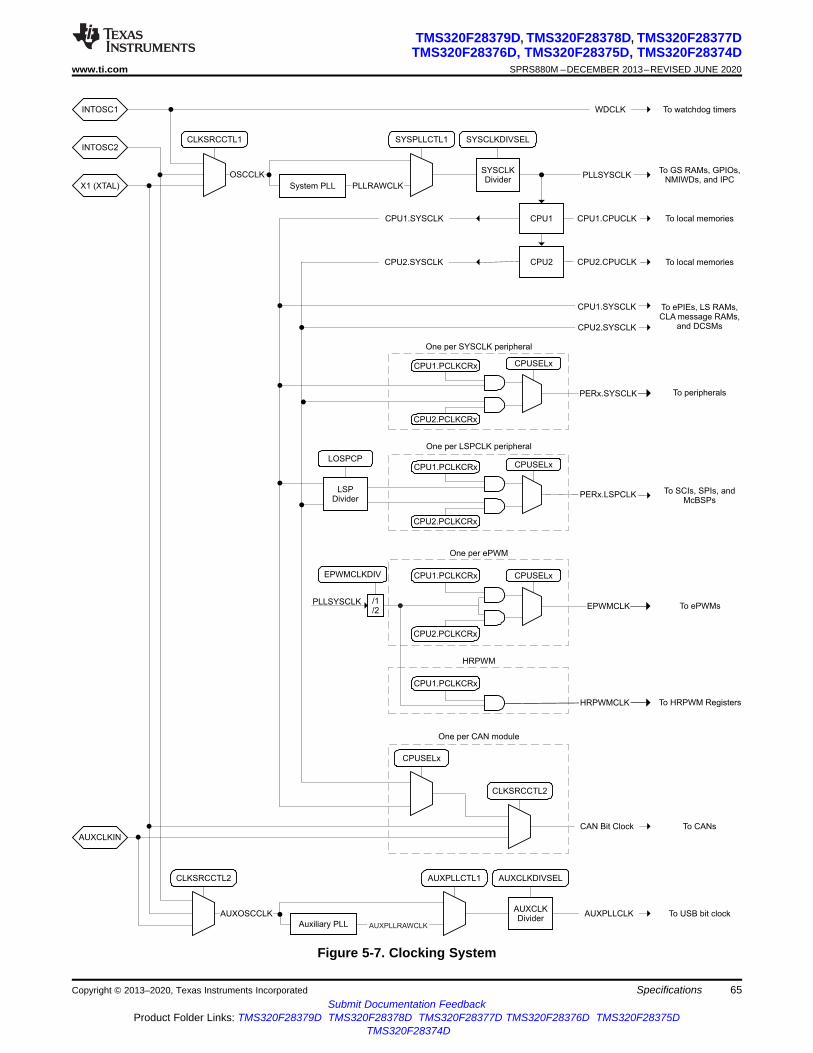
PLLSYSCLK
System PLL
CPU1
CPU2
Auxiliary PLL
LSPDivider
OSCCLK
AUXOSCCLK
AUXPLLRAWCLK
AUXPLLCLK
PLLRAWCLK
CPU1.CPUCLK
CPU2.CPUCLKCPU2.SYSCLK
CPU1.SYSCLK
PLLSYSCLK
CPUSELxCPU1.PCLKCRx
LOSPCP
To GS RAMs, GPIOs,NMIWDs, and IPC
To ePWMs
To SCIs, SPIs, andMcBSPs
To USB bit clock
To watchdog timersWDCLK
CLKSRCCTL1
CLKSRCCTL2 AUXPLLCTL1
SYSPLLCTL1
One per SYSCLK peripheral
One per LSPCLK peripheral
SYSCLKDivider
SYSCLKDIVSEL
INTOSC1
INTOSC2
X1 (XTAL)
AUXCLKIN
AUXCLKDivider
AUXCLKDIVSEL
CAN Bit Clock
CLKSRCCTL2
To CANs
CPUSELx
One per CAN module
CPU2.SYSCLK
To ePIEs, LS RAMs,CLA message RAMs,
and DCSMs
To local memories
To local memories
CPU1.SYSCLK
To peripherals
One per ePWM
EPWMCLK
EPWMCLKDIV
/1/2
CPU2.PCLKCRx
CPUSELxCPU1.PCLKCRx
CPU2.PCLKCRx
PERx.LSPCLK
PERx.SYSCLK
CPUSELxCPU1.PCLKCRx
CPU2.PCLKCRx
CPU1.PCLKCRx
To HRPWM Registers
HRPWM
HRPWMCLK
65
TMS320F28379D, TMS320F28378D, TMS320F28377DTMS320F28376D, TMS320F28375D, TMS320F28374D
www.ti.com SPRS880M –DECEMBER 2013–REVISED JUNE 2020
Submit Documentation FeedbackProduct Folder Links: TMS320F28379D TMS320F28378D TMS320F28377D TMS320F28376D TMS320F28375D
TMS320F28374D
SpecificationsCopyright © 2013–2020, Texas Instruments Incorporated
Figure 5-7. Clocking System

66
TMS320F28379D, TMS320F28378D, TMS320F28377DTMS320F28376D, TMS320F28375D, TMS320F28374DSPRS880M –DECEMBER 2013–REVISED JUNE 2020 www.ti.com
Submit Documentation FeedbackProduct Folder Links: TMS320F28379D TMS320F28378D TMS320F28377D TMS320F28376D TMS320F28375D
TMS320F28374D
Specifications Copyright © 2013–2020, Texas Instruments Incorporated
5.9.3.2 Clock Frequencies, Requirements, and Characteristics
This section provides the frequencies and timing requirements of the input clocks, PLL lock times,frequencies of the internal clocks, and the frequency and switching characteristics of the output clock.
5.9.3.2.1 Input Clock Frequency and Timing Requirements, PLL Lock Times
Table 5-7 shows the frequency requirements for the input clocks. Table 5-16 shows the crystal equivalentseries resistance requirements. Table 5-8 shows the X1 input level characteristics when using an externalclock source. Table 5-9 and Table 5-10 show the timing requirements for the input clocks. Table 5-11shows the PLL lock times for the Main PLL and the USB PLL.
Table 5-7. Input Clock FrequencyMIN MAX UNIT
f(XTAL) Frequency, X1/X2, from external crystal or resonator 10 20 MHzf(X1) Frequency, X1, from external oscillator 2 25 MHzf(AUXI) Frequency, AUXCLKIN, from external oscillator 2 60 MHz
Table 5-8. X1 Input Level Characteristics When Using an External Clock Source (Not a Crystal)over recommended operating conditions (unless otherwise noted)
PARAMETER MIN MAX UNITX1 VIL Valid low-level input voltage –0.3 0.3 * VDDIO VX1 VIH Valid high-level input voltage 0.7 * VDDIO VDDIO + 0.3 V
Table 5-9. X1 Timing RequirementsMIN MAX UNIT
tf(X1) Fall time, X1 6 nstr(X1) Rise time, X1 6 nstw(X1L) Pulse duration, X1 low as a percentage of tc(X1) 45% 55%tw(X1H) Pulse duration, X1 high as a percentage of tc(X1) 45% 55%
Table 5-10. AUXCLKIN Timing RequirementsMIN MAX UNIT
tf(AUXI) Fall time, AUXCLKIN 6 nstr(AUXI) Rise time, AUXCLKIN 6 nstw(AUXL) Pulse duration, AUXCLKIN low as a percentage of tc(XCI) 45% 55%tw(AUXH) Pulse duration, AUXCLKIN high as a percentage of tc(XCI) 45% 55%
(1) The PLL lock time here defines the typical time of execution for the PLL workaround as defined in the TMS320F2837xD Dual-CoreMCUs Silicon Errata. Cycle count includes code execution of the PLL initialization routine, which could vary depending on compileroptimizations and flash wait states. TI recommends using the latest example software from C2000Ware for initializing the PLLs. For thesystem PLL, see InitSysPll() or SysCtl_setClock(). For the auxillary PLL, see InitAuxPll() or SysCtl_setAuxClock().
Table 5-11. PLL Lock TimesMIN NOM MAX UNIT
t(PLL) Lock time, Main PLL (X1, from external oscillator) 50 µs + 2500 * tc(OSCCLK)(1) µs
t(USB) Lock time, USB PLL (AUXCLKIN, from external oscillator) 50 µs + 2500 * tc(OSCCLK)(1) µs
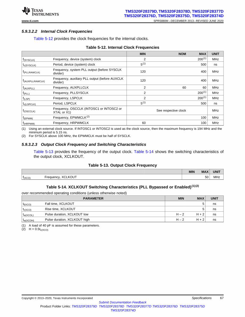
67
TMS320F28379D, TMS320F28378D, TMS320F28377DTMS320F28376D, TMS320F28375D, TMS320F28374D
www.ti.com SPRS880M –DECEMBER 2013–REVISED JUNE 2020
Submit Documentation FeedbackProduct Folder Links: TMS320F28379D TMS320F28378D TMS320F28377D TMS320F28376D TMS320F28375D
TMS320F28374D
SpecificationsCopyright © 2013–2020, Texas Instruments Incorporated
5.9.3.2.2 Internal Clock Frequencies
Table 5-12 provides the clock frequencies for the internal clocks.
(1) Using an external clock source. If INTOSC1 or INTOSC2 is used as the clock source, then the maximum frequency is 194 MHz and theminimum period is 5.15 ns.
(2) For SYSCLK above 100 MHz, the EPWMCLK must be half of SYSCLK.
Table 5-12. Internal Clock FrequenciesMIN NOM MAX UNIT
f(SYSCLK) Frequency, device (system) clock 2 200 (1) MHztc(SYSCLK) Period, device (system) clock 5 (1) 500 ns
f(PLLRAWCLK)Frequency, system PLL output (before SYSCLKdivider) 120 400 MHz
f(AUXPLLRAWCLK)Frequency, auxiliary PLL output (before AUXCLKdivider) 120 400 MHz
f(AUXPLL) Frequency, AUXPLLCLK 2 60 60 MHzf(PLL) Frequency, PLLSYSCLK 2 200 (1) MHzf(LSP) Frequency, LSPCLK 2 200 (1) MHztc(LSPCLK) Period, LSPCLK 5 (1) 500 ns
f(OSCCLK)Frequency, OSCCLK (INTOSC1 or INTOSC2 orXTAL or X1) See respective clock MHz
f(EPWM) Frequency, EPWMCLK (2) 100 MHzf(HRPWM) Frequency, HRPWMCLK 60 100 MHz
5.9.3.2.3 Output Clock Frequency and Switching Characteristics
Table 5-13 provides the frequency of the output clock. Table 5-14 shows the switching characteristics ofthe output clock, XCLKOUT.
Table 5-13. Output Clock FrequencyMIN MAX UNIT
f(XCO) Frequency, XCLKOUT 50 MHz
(1) A load of 40 pF is assumed for these parameters.(2) H = 0.5tc(XCO)
Table 5-14. XCLKOUT Switching Characteristics (PLL Bypassed or Enabled) (1) (2)
over recommended operating conditions (unless otherwise noted)PARAMETER MIN MAX UNIT
tf(XCO) Fall time, XCLKOUT 5 nstr(XCO) Rise time, XCLKOUT 5 nstw(XCOL) Pulse duration, XCLKOUT low H – 2 H + 2 nstw(XCOH) Pulse duration, XCLKOUT high H – 2 H + 2 ns
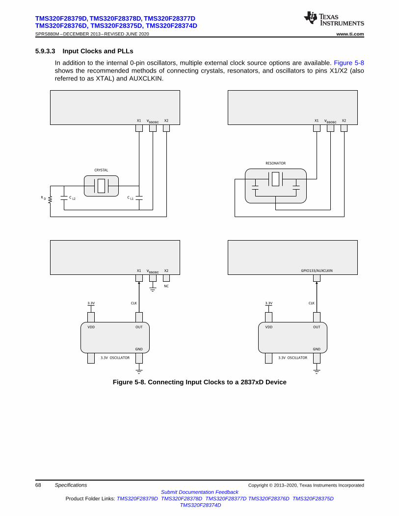
X1 X2
CRYSTAL
X1 X2
X1 X2
3.3V
OUTVDD
GND
CLK
R D C L2 C L1
RESONATOR
3.3V OSCILLATOR
NC
vssosc
GPIO133/AUXCLKIN
3.3V
OUTVDD
GND
CLK
3.3V OSCILLATOR
vssosc
vssosc
68
TMS320F28379D, TMS320F28378D, TMS320F28377DTMS320F28376D, TMS320F28375D, TMS320F28374DSPRS880M –DECEMBER 2013–REVISED JUNE 2020 www.ti.com
Submit Documentation FeedbackProduct Folder Links: TMS320F28379D TMS320F28378D TMS320F28377D TMS320F28376D TMS320F28375D
TMS320F28374D
Specifications Copyright © 2013–2020, Texas Instruments Incorporated
5.9.3.3 Input Clocks and PLLs
In addition to the internal 0-pin oscillators, multiple external clock source options are available. Figure 5-8shows the recommended methods of connecting crystals, resonators, and oscillators to pins X1/X2 (alsoreferred to as XTAL) and AUXCLKIN.
Figure 5-8. Connecting Input Clocks to a 2837xD Device

69
TMS320F28379D, TMS320F28378D, TMS320F28377DTMS320F28376D, TMS320F28375D, TMS320F28374D
www.ti.com SPRS880M –DECEMBER 2013–REVISED JUNE 2020
Submit Documentation FeedbackProduct Folder Links: TMS320F28379D TMS320F28378D TMS320F28377D TMS320F28376D TMS320F28375D
TMS320F28374D
SpecificationsCopyright © 2013–2020, Texas Instruments Incorporated
5.9.3.4 Crystal Oscillator
When using a quartz crystal, it may be necessary to include a damping resistor (RD) in the crystal circuit toprevent over-driving the crystal (drive level can be found in the crystal data sheet). In higher-frequencyapplications (10 MHz or greater), RD is generally not required. If a damping resistor is required, RD shouldbe as small as possible because the size of the resistance affects start-up time (smaller RD = faster start-up time). TI recommends that the crystal manufacturer characterize the crystal with the application board.Table 5-15 shows the crystal oscillator parameters. Table 5-16 shows the crystal equivalent seriesresistance (ESR) requirements. Table 5-17 shows the crystal oscillator electrical characteristics.
Table 5-15. Crystal Oscillator ParametersMIN MAX UNIT
CL1, CL2 Load capacitance 12 24 pFC0 Crystal shunt capacitance 7 pF
(1) Crystal shunt capacitance (C0) should be less than or equal to 7 pF.(2) ESR = Negative Resistance/3
Table 5-16. Crystal Equivalent Series Resistance (ESR) Requirements (1) (2)
CRYSTAL FREQUENCY (MHz) MAXIMUM ESR (Ω)(CL1 = CL2 = 12 pF)
MAXIMUM ESR (Ω)(CL1 = CL2 = 24 pF)
10 55 11012 50 9514 50 9016 45 7518 45 6520 45 50
(1) Start-up time is dependent on the crystal and tank circuit components. TI recommends that the crystal vendor characterize theapplication with the chosen crystal.
Table 5-17. Crystal Oscillator Electrical Characteristicsover recommended operating conditions (unless otherwise noted)
PARAMETER TEST CONDITIONS MIN TYP MAX UNIT
Start-up time (1)
f = 20 MHzESR MAX = 50 ΩCL1 = CL2 = 24 pFC0 = 7 pF
2 ms
Crystal drive level (DL) 1 mW
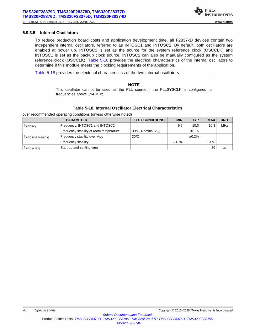
70
TMS320F28379D, TMS320F28378D, TMS320F28377DTMS320F28376D, TMS320F28375D, TMS320F28374DSPRS880M –DECEMBER 2013–REVISED JUNE 2020 www.ti.com
Submit Documentation FeedbackProduct Folder Links: TMS320F28379D TMS320F28378D TMS320F28377D TMS320F28376D TMS320F28375D
TMS320F28374D
Specifications Copyright © 2013–2020, Texas Instruments Incorporated
5.9.3.5 Internal Oscillators
To reduce production board costs and application development time, all F2837xD devices contain twoindependent internal oscillators, referred to as INTOSC1 and INTOSC2. By default, both oscillators areenabled at power up. INTOSC2 is set as the source for the system reference clock (OSCCLK) andINTOSC1 is set as the backup clock source. INTOSC1 can also be manually configured as the systemreference clock (OSCCLK). Table 5-18 provides the electrical characteristics of the internal oscillators todetermine if this module meets the clocking requirements of the application.
Table 5-18 provides the electrical characteristics of the two internal oscillators.
NOTEThis oscillator cannot be used as the PLL source if the PLLSYSCLK is configured tofrequencies above 194 MHz.
Table 5-18. Internal Oscillator Electrical Characteristicsover recommended operating conditions (unless otherwise noted)
PARAMETER TEST CONDITIONS MIN TYP MAX UNITf(INTOSC) Frequency, INTOSC1 and INTOSC2 9.7 10.0 10.3 MHz
f(INTOSC-STABILITY)
Frequency stability at room temperature 30ºC, Nominal VDD ±0.1%Frequency stability over VDD 30ºC ±0.2%Frequency stability –3.0% 3.0%
f(INTOSC-ST) Start-up and settling time 20 µs

71
TMS320F28379D, TMS320F28378D, TMS320F28377DTMS320F28376D, TMS320F28375D, TMS320F28374D
www.ti.com SPRS880M –DECEMBER 2013–REVISED JUNE 2020
Submit Documentation FeedbackProduct Folder Links: TMS320F28379D TMS320F28378D TMS320F28377D TMS320F28376D TMS320F28375D
TMS320F28374D
SpecificationsCopyright © 2013–2020, Texas Instruments Incorporated
(1) Minimum required FRDCNTL[RWAIT].
5.9.4 Flash ParametersThe on-chip flash memory is tightly integrated to the CPU, allowing code execution directly from flashthrough 128-bit-wide prefetch reads and a pipeline buffer. Flash performance for sequential code is equalto execution from RAM. Factoring in discontinuities, most applications will run with an efficiency ofapproximately 80% relative to code executing from RAM. This flash efficiency lets designers realize a 2×improvement in performance when migrating from the previous generation of MCUs.
This device also has an OTP (One-Time-Programmable) sector used for the dual code security module(DCSM), which cannot be erased after it is programmed.
Table 5-19 shows the minimum required flash wait states at different frequencies. Table 5-20 shows theflash parameters.
Table 5-19. Flash Wait States
CPUCLK (MHz)MINIMUM WAIT STATES (1)
EXTERNAL OSCILLATOR OR CRYSTAL INTOSC1 OR INTOSC2150 < CPUCLK ≤ 200 145 < CPUCLK ≤ 194 3100 < CPUCLK ≤ 150 97 < CPUCLK ≤ 145 250 < CPUCLK ≤ 100 48 < CPUCLK ≤ 97 1
CPUCLK ≤ 50 CPUCLK ≤ 48 0
(1) Program time is at the maximum device frequency. Program time includes overhead of the flash state machine but does not include thetime to transfer the following into RAM:• Code that uses flash API to program the flash• Flash API itself• Flash data to be programmedIn other words, the time indicated in this table is applicable after all the required code/data is available in the device RAM, ready forprogramming. The transfer time will significantly vary depending on the speed of the JTAG debug probe used.Program time calculation is based on programming 144 bits at a time at the specified operating frequency. Program time includesProgram verify by the CPU. The program time does not degrade with write/erase (W/E) cycling, but the erase time does.Erase time includes Erase verify by the CPU and does not involve any data transfer.
(2) Erase time includes Erase verify by the CPU.
Table 5-20. Flash ParametersPARAMETER MIN TYP MAX UNIT
Program Time (1)
128 data bits + 16 ECC bits 40 300 µs8KW sector 90 180 ms32KW sector 360 720 ms
Erase Time (2) at < 25 cycles8KW sector 25 50
ms32KW sector 30 55
Erase Time (2) at 20k cycles8KW sector 105 4000
ms32KW sector 110 4000
Nwec Write/erase cycles 20000 cyclestretention Data retention duration at TJ = 85°C 20 years
NOTEThe Main Array flash programming must be aligned to 64-bit address boundaries and each64-bit word may only be programmed once per write/erase cycle. For more details, see the"Flash: Minimum Programming Word Size" advisory in the TMS320F2837xD Dual-CoreMCUs Silicon Errata.

TMS
TDI
TDO
PD
RTCK
TCK
EMU0
TRST
TDIS
GND
KEY
GND
GND
EMU1
GND
TCK
TDO
TDI
TMS
TRST GND
1 2
3 4
5 6
7 8
9 10
11 12
14133.3 V3.3 V
100 W
2.2 kW
4.7 kW4.7 kW
3.3 V
Distance between the header and the target
should be less than 6 inches (15.24 cm).
MCU
72
TMS320F28379D, TMS320F28378D, TMS320F28377DTMS320F28376D, TMS320F28375D, TMS320F28374DSPRS880M –DECEMBER 2013–REVISED JUNE 2020 www.ti.com
Submit Documentation FeedbackProduct Folder Links: TMS320F28379D TMS320F28378D TMS320F28377D TMS320F28376D TMS320F28375D
TMS320F28374D
Specifications Copyright © 2013–2020, Texas Instruments Incorporated
5.9.5 Emulation/JTAGThe JTAG port has five dedicated pins: TRST, TMS, TDI, TDO, and TCK. The TRST signal should alwaysbe pulled down through a 2.2-kΩ pulldown resistor on the board. This MCU does not support the EMU0and EMU1 signals that are present on 14-pin and 20-pin emulation headers. These signals should alwaysbe pulled up at the emulation header through a pair of board pullup resistors ranging from 2.2 kΩ to4.7 kΩ (depending on the drive strength of the debugger ports). Typically, a 2.2-kΩ value is used.
See Figure 5-9 to see how the 14-pin JTAG header connects to the MCU’s JTAG port signals. Figure 5-10shows how to connect to the 20-pin header. The 20-pin JTAG header terminals EMU2, EMU3, and EMU4are not used and should be grounded.
The PD (Power Detect) terminal of the JTAG debug probe header should be connected to the board 3.3-Vsupply. Header GND terminals should be connected to board ground. TDIS (Cable Disconnect Sense)should also be connected to board ground. The JTAG clock should be looped from the header TCK outputterminal back to the RTCK input terminal of the header (to sense clock continuity by the JTAG debugprobe). Header terminal RESET is an open-drain output from the JTAG debug probe header that enablesboard components to be reset through JTAG debug probe commands (available only through the 20-pinheader).
Typically, no buffers are needed on the JTAG signals when the distance between the MCU target and theJTAG header is smaller than 6 inches (15.24 cm), and no other devices are present on the JTAG chain.Otherwise, each signal should be buffered. Additionally, for most JTAG debug probe operations at10 MHz, no series resistors are needed on the JTAG signals. However, if high emulation speeds areexpected (35 MHz or so), 22-Ω resistors should be placed in series on each JTAG signal.
For more information about hardware breakpoints and watchpoints, see Hardware Breakpoints andWatchpoints for C28x in CCS.
For more information about JTAG emulation, see the XDS Target Connection Guide.
Figure 5-9. Connecting to the 14-Pin JTAG Header
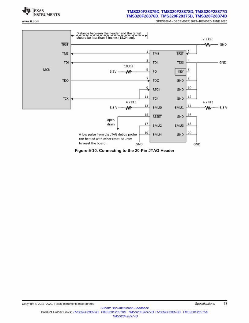
TMS
TDI
TDO
PD
RTCK
TCK
EMU0
TRST
TDIS
GND
KEY
GND
GND
EMU1
GND
GND
TCK
TDO
TDI
TMS
TRST
RESET
EMU2
EMU4
EMU3
GND
GND
open
drain
A low pulse from the JTAG debug probe
can be tied with other reset sources
to reset the board.
1 2
3 4
5 6
7 8
9 10
11 12
1413
1615
1817
2019
3.3 V3.3 V
3.3V
100 W
2.2 kW
4.7 kW4.7 kW
GND
GND
MCU
Distance between the header and the target
should be less than 6 inches (15.24 cm).
73
TMS320F28379D, TMS320F28378D, TMS320F28377DTMS320F28376D, TMS320F28375D, TMS320F28374D
www.ti.com SPRS880M –DECEMBER 2013–REVISED JUNE 2020
Submit Documentation FeedbackProduct Folder Links: TMS320F28379D TMS320F28378D TMS320F28377D TMS320F28376D TMS320F28375D
TMS320F28374D
SpecificationsCopyright © 2013–2020, Texas Instruments Incorporated
Figure 5-10. Connecting to the 20-Pin JTAG Header
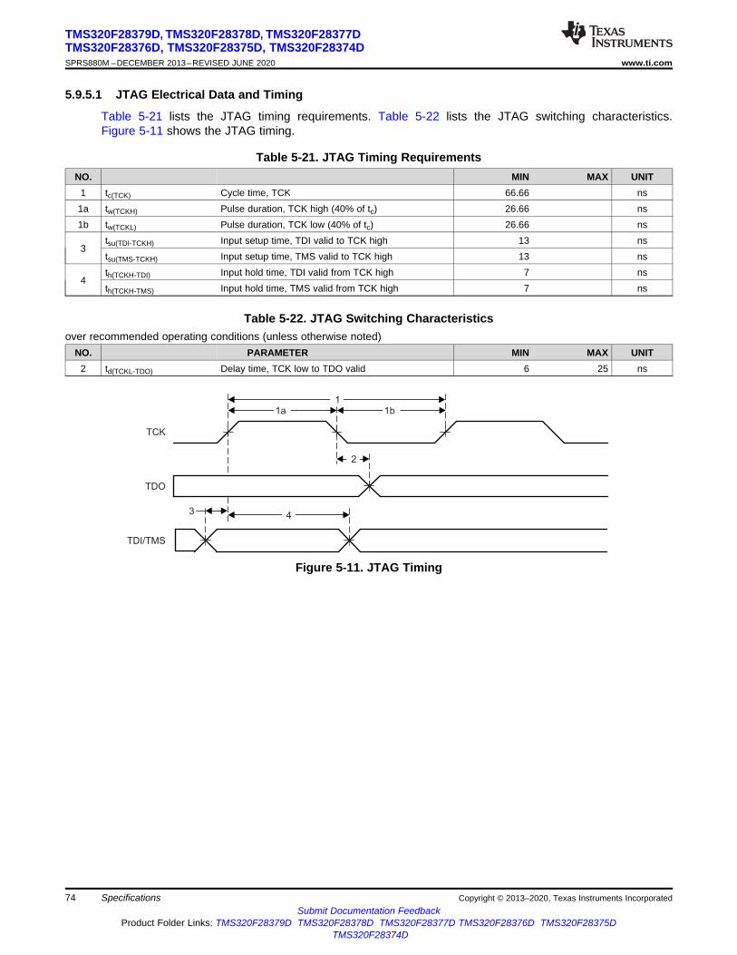
3
TCK
TDO
TDI/TMS
2
4
1
1a 1b
74
TMS320F28379D, TMS320F28378D, TMS320F28377DTMS320F28376D, TMS320F28375D, TMS320F28374DSPRS880M –DECEMBER 2013–REVISED JUNE 2020 www.ti.com
Submit Documentation FeedbackProduct Folder Links: TMS320F28379D TMS320F28378D TMS320F28377D TMS320F28376D TMS320F28375D
TMS320F28374D
Specifications Copyright © 2013–2020, Texas Instruments Incorporated
5.9.5.1 JTAG Electrical Data and Timing
Table 5-21 lists the JTAG timing requirements. Table 5-22 lists the JTAG switching characteristics.Figure 5-11 shows the JTAG timing.
Table 5-21. JTAG Timing RequirementsNO. MIN MAX UNIT
1 tc(TCK) Cycle time, TCK 66.66 ns1a tw(TCKH) Pulse duration, TCK high (40% of tc) 26.66 ns1b tw(TCKL) Pulse duration, TCK low (40% of tc) 26.66 ns
3tsu(TDI-TCKH) Input setup time, TDI valid to TCK high 13 nstsu(TMS-TCKH) Input setup time, TMS valid to TCK high 13 ns
4th(TCKH-TDI) Input hold time, TDI valid from TCK high 7 nsth(TCKH-TMS) Input hold time, TMS valid from TCK high 7 ns
Table 5-22. JTAG Switching Characteristicsover recommended operating conditions (unless otherwise noted)
NO. PARAMETER MIN MAX UNIT2 td(TCKL-TDO) Delay time, TCK low to TDO valid 6 25 ns
Figure 5-11. JTAG Timing

GPIO
tf(GPO)
tr(GPO)
75
TMS320F28379D, TMS320F28378D, TMS320F28377DTMS320F28376D, TMS320F28375D, TMS320F28374D
www.ti.com SPRS880M –DECEMBER 2013–REVISED JUNE 2020
Submit Documentation FeedbackProduct Folder Links: TMS320F28379D TMS320F28378D TMS320F28377D TMS320F28376D TMS320F28375D
TMS320F28374D
SpecificationsCopyright © 2013–2020, Texas Instruments Incorporated
(1) Rise time and fall time vary with load. These values assume a 40-pF load.
5.9.6 GPIO Electrical Data and TimingThe peripheral signals are multiplexed with general-purpose input/output (GPIO) signals. On reset, GPIOpins are configured as inputs. For specific inputs, the user can also select the number of input qualificationcycles to filter unwanted noise glitches.
The GPIO module contains an Output X-BAR which allows an assortment of internal signals to be routedto a GPIO in the GPIO mux positions denoted as OUTPUTXBARx. The GPIO module also contains anInput X-BAR which is used to route signals from any GPIO input to different IP blocks such as the ADC(s),eCAP(s), ePWM(s), and external interrupts. For more details, see the X-BAR chapter in theTMS320F2837xD Dual-Core Microcontrollers Technical Reference Manual.
5.9.6.1 GPIO - Output Timing
Table 5-23 shows the general-purpose output switching characteristics. Figure 5-12 shows the general-purpose output timing.
Table 5-23. General-Purpose Output Switching Characteristicsover recommended operating conditions (unless otherwise noted)
PARAMETER MIN MAX UNITtr(GPO) Rise time, GPIO switching low to high All GPIOs 8 (1) nstf(GPO) Fall time, GPIO switching high to low All GPIOs 8 (1) nstfGPO Toggling frequency, GPO pins 25 MHz
Figure 5-12. General-Purpose Output Timing

GPIO Signal
1
Sampling Window
1 1 1 1 1 1 1 1 1 1 10 0 0 0 0 0 0 0 0 0
SYSCLK
(A)
GPxQSELn = 1,0 (6 samples)
(D)
Output FromQualifier
QUALPRD = 1(SYSCLK/2)
tw(IQSW)
tw(SP)
(SYSCLK cycle * 2 * QUALPRD) * 5(C)
Sampling Period determined
by GPxCTRL[QUALPRD](B)
76
TMS320F28379D, TMS320F28378D, TMS320F28377DTMS320F28376D, TMS320F28375D, TMS320F28374DSPRS880M –DECEMBER 2013–REVISED JUNE 2020 www.ti.com
Submit Documentation FeedbackProduct Folder Links: TMS320F28379D TMS320F28378D TMS320F28377D TMS320F28376D TMS320F28375D
TMS320F28374D
Specifications Copyright © 2013–2020, Texas Instruments Incorporated
5.9.6.2 GPIO - Input Timing
Table 5-24 shows the general-purpose input timing requirements. Figure 5-13 shows the sampling mode.
(1) "n" represents the number of qualification samples as defined by GPxQSELn register.(2) For tw(GPI), pulse width is measured from VIL to VIL for an active low signal and VIH to VIH for an active high signal.
Table 5-24. General-Purpose Input Timing RequirementsMIN MAX UNIT
tw(SP) Sampling periodQUALPRD = 0 1tc(SYSCLK) cyclesQUALPRD ≠ 0 2tc(SYSCLK) * QUALPRD cycles
tw(IQSW) Input qualifier sampling window tw(SP) * (n (1) – 1) cycles
tw(GPI)(2) Pulse duration, GPIO low/high
Synchronous mode 2tc(SYSCLK) cyclesWith input qualifier tw(IQSW) + tw(SP) + 1tc(SYSCLK) cycles
A. This glitch will be ignored by the input qualifier. The QUALPRD bit field specifies the qualification sampling period. Itcan vary from 00 to 0xFF. If QUALPRD = 00, then the sampling period is 1 SYSCLK cycle. For any other value "n",the qualification sampling period in 2n SYSCLK cycles (that is, at every 2n SYSCLK cycles, the GPIO pin will besampled).
B. The qualification period selected through the GPxCTRL register applies to groups of 8 GPIO pins.C. The qualification block can take either three or six samples. The GPxQSELn Register selects which sample mode is
used.D. In the example shown, for the qualifier to detect the change, the input should be stable for 10 SYSCLK cycles or
greater. In other words, the inputs should be stable for (5 x QUALPRD x 2) SYSCLK cycles. This would ensure5 sampling periods for detection to occur. Because external signals are driven asynchronously, an 13-SYSCLK-widepulse ensures reliable recognition.
Figure 5-13. Sampling Mode

GPIOxn
SYSCLK
tw(GPI)
Sampling period = SYSCLK cycle 2 QUALPRD, if QUALPRD 0´ ¹´
Sampling frequency = SYSCLK, if QUALPRD 0=
Sampling frequency = SYSCLK/(2 QUALPRD), if QUALPRD 0´ ¹
77
TMS320F28379D, TMS320F28378D, TMS320F28377DTMS320F28376D, TMS320F28375D, TMS320F28374D
www.ti.com SPRS880M –DECEMBER 2013–REVISED JUNE 2020
Submit Documentation FeedbackProduct Folder Links: TMS320F28379D TMS320F28378D TMS320F28377D TMS320F28376D TMS320F28375D
TMS320F28374D
SpecificationsCopyright © 2013–2020, Texas Instruments Incorporated
5.9.6.3 Sampling Window Width for Input Signals
The following section summarizes the sampling window width for input signals for various input qualifierconfigurations.
Sampling frequency denotes how often a signal is sampled with respect to SYSCLK.(1)
(2)
(3)
In Equation 1, Equation 2, and Equation 3, SYSCLK cycle indicates the time period of SYSCLK.
Sampling period = SYSCLK cycle, if QUALPRD = 0
In a given sampling window, either 3 or 6 samples of the input signal are taken to determine the validity ofthe signal. This is determined by the value written to GPxQSELn register.
Case 1:
Qualification using 3 samplesSampling window width = (SYSCLK cycle × 2 × QUALPRD) × 2, if QUALPRD ≠ 0Sampling window width = (SYSCLK cycle) × 2, if QUALPRD = 0
Case 2:
Qualification using 6 samplesSampling window width = (SYSCLK cycle × 2 × QUALPRD) × 5, if QUALPRD ≠ 0Sampling window width = (SYSCLK cycle) × 5, if QUALPRD = 0
Figure 5-14 shows the general-purpose input timing.
Figure 5-14. General-Purpose Input Timing
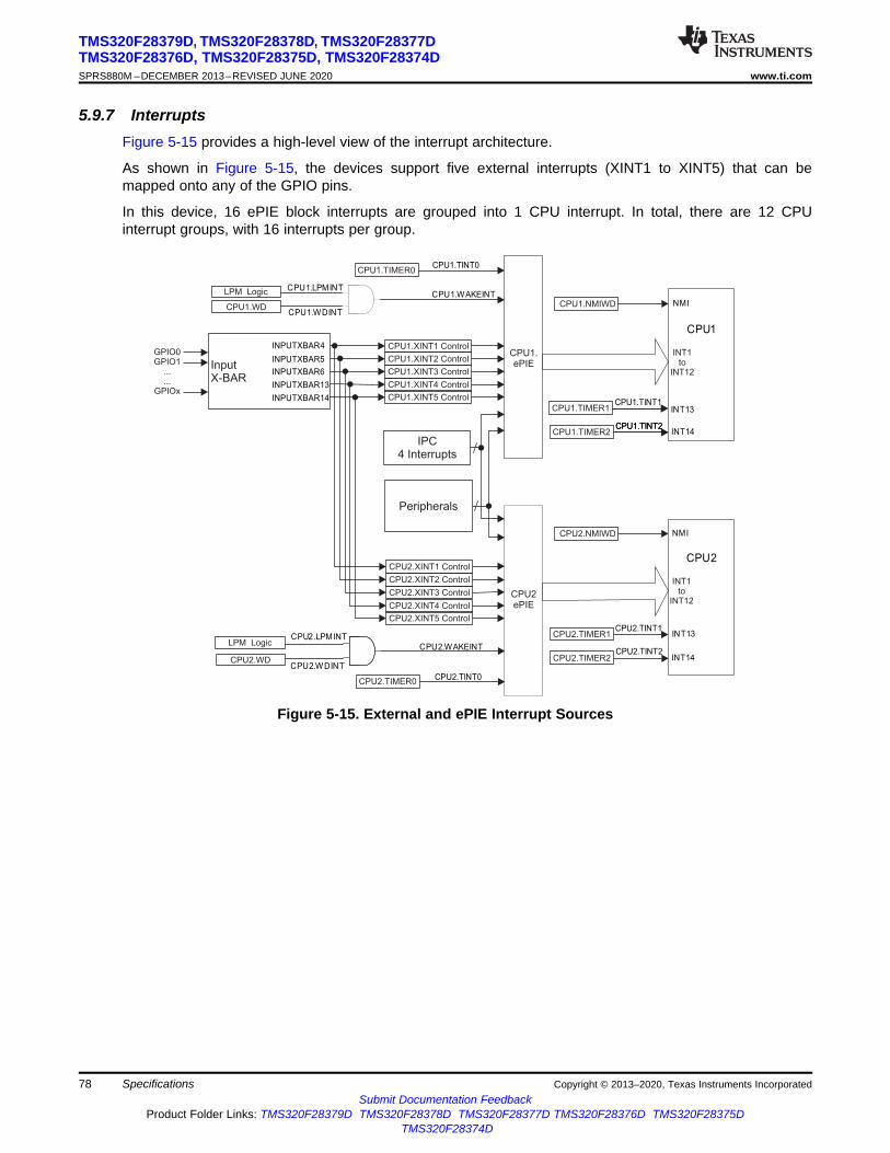
INPUTXBAR4
CPU1.WDINT
CPU2.WDINT
CPU1.LPMINT
CPU2.LPMINT
CPU1.WAKEINT
CPU2.WAKEINT
CPU1.TINT0
CPU1.ePIE
INT13
INT14
NMI
CPU1
INT1to
INT12
NMI
CPU2
INT1to
INT12
INPUTXBAR13
INPUTXBAR5
INPUTXBAR6
INPUTXBAR14
GPIO0GPIO1
...
...GPIOx
CPU1.TIMER0
CPU2.TINT0CPU2.TIMER0
CPU2ePIE
CPU1.TINT1CPU1.TIMER1
CPU1.TINT2CPU1.TIMER2
CPU1.TINT2
INT13
INT14
CPU2.TINT1CPU2.TIMER1
CPU2.TINT2CPU2.TIMER2
LPM Logic
CPU2.WD
Peripherals
IPC4 Interrupts
CPU1.XINT1 Control
CPU1.XINT5 Control
CPU1.XINT3 Control
CPU1.XINT4 Control
CPU1.XINT2 Control
CPU2.XINT1 Control
CPU2.XINT5 Control
CPU2.XINT3 Control
CPU2.XINT4 Control
CPU2.XINT2 Control
InputX-BAR
LPM Logic
CPU1.WD CPU1.NMIWD
CPU2.NMIWD
78
TMS320F28379D, TMS320F28378D, TMS320F28377DTMS320F28376D, TMS320F28375D, TMS320F28374DSPRS880M –DECEMBER 2013–REVISED JUNE 2020 www.ti.com
Submit Documentation FeedbackProduct Folder Links: TMS320F28379D TMS320F28378D TMS320F28377D TMS320F28376D TMS320F28375D
TMS320F28374D
Specifications Copyright © 2013–2020, Texas Instruments Incorporated
5.9.7 InterruptsFigure 5-15 provides a high-level view of the interrupt architecture.
As shown in Figure 5-15, the devices support five external interrupts (XINT1 to XINT5) that can bemapped onto any of the GPIO pins.
In this device, 16 ePIE block interrupts are grouped into 1 CPU interrupt. In total, there are 12 CPUinterrupt groups, with 16 interrupts per group.
Figure 5-15. External and ePIE Interrupt Sources
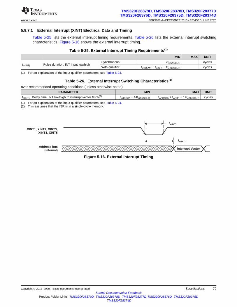
Interrupt Vector
XINT1, XINT2, XINT3,XINT4, XINT5
Address bus(internal)
tw(INT)
td(INT)
79
TMS320F28379D, TMS320F28378D, TMS320F28377DTMS320F28376D, TMS320F28375D, TMS320F28374D
www.ti.com SPRS880M –DECEMBER 2013–REVISED JUNE 2020
Submit Documentation FeedbackProduct Folder Links: TMS320F28379D TMS320F28378D TMS320F28377D TMS320F28376D TMS320F28375D
TMS320F28374D
SpecificationsCopyright © 2013–2020, Texas Instruments Incorporated
5.9.7.1 External Interrupt (XINT) Electrical Data and Timing
Table 5-25 lists the external interrupt timing requirements. Table 5-26 lists the external interrupt switchingcharacteristics. Figure 5-16 shows the external interrupt timing.
(1) For an explanation of the input qualifier parameters, see Table 5-24.
Table 5-25. External Interrupt Timing Requirements (1)
MIN MAX UNIT
tw(INT) Pulse duration, INT input low/highSynchronous 2tc(SYSCLK) cyclesWith qualifier tw(IQSW) + tw(SP) + 1tc(SYSCLK) cycles
(1) For an explanation of the input qualifier parameters, see Table 5-24.(2) This assumes that the ISR is in a single-cycle memory.
Table 5-26. External Interrupt Switching Characteristics (1)
over recommended operating conditions (unless otherwise noted)PARAMETER MIN MAX UNIT
td(INT) Delay time, INT low/high to interrupt-vector fetch (2) tw(IQSW) + 14tc(SYSCLK) tw(IQSW) + tw(SP) + 14tc(SYSCLK) cycles
Figure 5-16. External Interrupt Timing
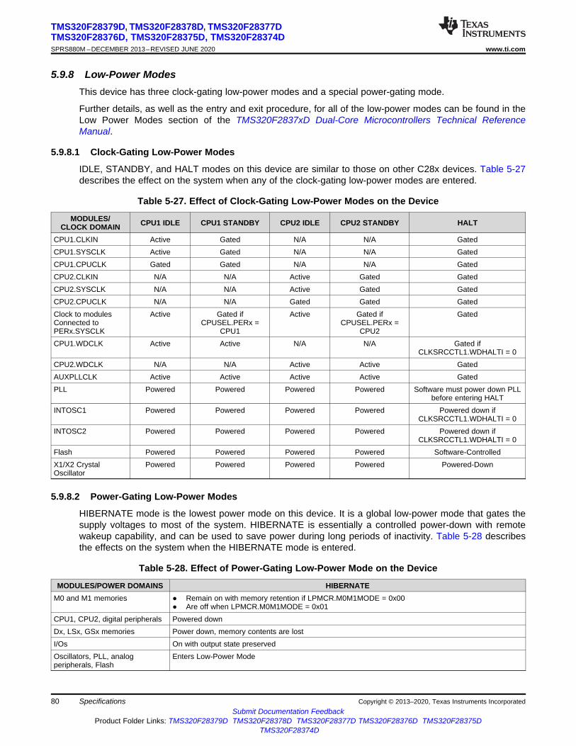
80
TMS320F28379D, TMS320F28378D, TMS320F28377DTMS320F28376D, TMS320F28375D, TMS320F28374DSPRS880M –DECEMBER 2013–REVISED JUNE 2020 www.ti.com
Submit Documentation FeedbackProduct Folder Links: TMS320F28379D TMS320F28378D TMS320F28377D TMS320F28376D TMS320F28375D
TMS320F28374D
Specifications Copyright © 2013–2020, Texas Instruments Incorporated
5.9.8 Low-Power ModesThis device has three clock-gating low-power modes and a special power-gating mode.
Further details, as well as the entry and exit procedure, for all of the low-power modes can be found in theLow Power Modes section of the TMS320F2837xD Dual-Core Microcontrollers Technical ReferenceManual.
5.9.8.1 Clock-Gating Low-Power Modes
IDLE, STANDBY, and HALT modes on this device are similar to those on other C28x devices. Table 5-27describes the effect on the system when any of the clock-gating low-power modes are entered.
Table 5-27. Effect of Clock-Gating Low-Power Modes on the Device
MODULES/CLOCK DOMAIN CPU1 IDLE CPU1 STANDBY CPU2 IDLE CPU2 STANDBY HALT
CPU1.CLKIN Active Gated N/A N/A GatedCPU1.SYSCLK Active Gated N/A N/A GatedCPU1.CPUCLK Gated Gated N/A N/A GatedCPU2.CLKIN N/A N/A Active Gated GatedCPU2.SYSCLK N/A N/A Active Gated GatedCPU2.CPUCLK N/A N/A Gated Gated GatedClock to modulesConnected toPERx.SYSCLK
Active Gated ifCPUSEL.PERx =
CPU1
Active Gated ifCPUSEL.PERx =
CPU2
Gated
CPU1.WDCLK Active Active N/A N/A Gated ifCLKSRCCTL1.WDHALTI = 0
CPU2.WDCLK N/A N/A Active Active GatedAUXPLLCLK Active Active Active Active GatedPLL Powered Powered Powered Powered Software must power down PLL
before entering HALTINTOSC1 Powered Powered Powered Powered Powered down if
CLKSRCCTL1.WDHALTI = 0INTOSC2 Powered Powered Powered Powered Powered down if
CLKSRCCTL1.WDHALTI = 0Flash Powered Powered Powered Powered Software-ControlledX1/X2 CrystalOscillator
Powered Powered Powered Powered Powered-Down
5.9.8.2 Power-Gating Low-Power Modes
HIBERNATE mode is the lowest power mode on this device. It is a global low-power mode that gates thesupply voltages to most of the system. HIBERNATE is essentially a controlled power-down with remotewakeup capability, and can be used to save power during long periods of inactivity. Table 5-28 describesthe effects on the system when the HIBERNATE mode is entered.
Table 5-28. Effect of Power-Gating Low-Power Mode on the Device
MODULES/POWER DOMAINS HIBERNATEM0 and M1 memories Remain on with memory retention if LPMCR.M0M1MODE = 0x00
Are off when LPMCR.M0M1MODE = 0x01CPU1, CPU2, digital peripherals Powered downDx, LSx, GSx memories Power down, memory contents are lostI/Os On with output state preservedOscillators, PLL, analogperipherals, Flash
Enters Low-Power Mode
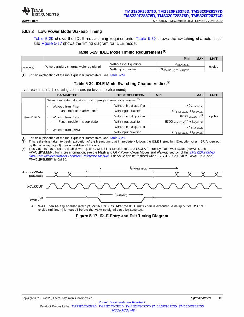
WAKE(A)
XCLKOUT
Address/Data(internal)
tw(WAKE)
td(WAKE-IDLE)
81
TMS320F28379D, TMS320F28378D, TMS320F28377DTMS320F28376D, TMS320F28375D, TMS320F28374D
www.ti.com SPRS880M –DECEMBER 2013–REVISED JUNE 2020
Submit Documentation FeedbackProduct Folder Links: TMS320F28379D TMS320F28378D TMS320F28377D TMS320F28376D TMS320F28375D
TMS320F28374D
SpecificationsCopyright © 2013–2020, Texas Instruments Incorporated
5.9.8.3 Low-Power Mode Wakeup Timing
Table 5-29 shows the IDLE mode timing requirements, Table 5-30 shows the switching characteristics,and Figure 5-17 shows the timing diagram for IDLE mode.
(1) For an explanation of the input qualifier parameters, see Table 5-24.
Table 5-29. IDLE Mode Timing Requirements (1)
MIN MAX UNIT
tw(WAKE) Pulse duration, external wake-up signalWithout input qualifier 2tc(SYSCLK) cyclesWith input qualifier 2tc(SYSCLK) + tw(IQSW)
(1) For an explanation of the input qualifier parameters, see Table 5-24.(2) This is the time taken to begin execution of the instruction that immediately follows the IDLE instruction. Execution of an ISR (triggered
by the wake-up signal) involves additional latency.(3) This value is based on the flash power-up time, which is a function of the SYSCLK frequency, flash wait states (RWAIT), and
FPAC1[PSLEEP]. For more information, see the Flash and OTP Power-Down Modes and Wakeup section of the TMS320F2837xDDual-Core Microcontrollers Technical Reference Manual. This value can be realized when SYSCLK is 200 MHz, RWAIT is 3, andFPAC1[PSLEEP] is 0x860.
Table 5-30. IDLE Mode Switching Characteristics (1)
over recommended operating conditions (unless otherwise noted)PARAMETER TEST CONDITIONS MIN MAX UNIT
td(WAKE-IDLE)
Delay time, external wake signal to program execution resume (2)
cycles
• Wakeup from Flash– Flash module in active state
Without input qualifier 40tc(SYSCLK)
With input qualifier 40tc(SYSCLK) + tw(WAKE)
• Wakeup from Flash– Flash module in sleep state
Without input qualifier 6700tc(SYSCLK)(3)
With input qualifier 6700tc(SYSCLK)(3) + tw(WAKE)
• Wakeup from RAMWithout input qualifier 25tc(SYSCLK)
With input qualifier 25tc(SYSCLK) + tw(WAKE)
A. WAKE can be any enabled interrupt, WDINT or XRS. After the IDLE instruction is executed, a delay of five OSCCLKcycles (minimum) is needed before the wake-up signal could be asserted.
Figure 5-17. IDLE Entry and Exit Timing Diagram

82
TMS320F28379D, TMS320F28378D, TMS320F28377DTMS320F28376D, TMS320F28375D, TMS320F28374DSPRS880M –DECEMBER 2013–REVISED JUNE 2020 www.ti.com
Submit Documentation FeedbackProduct Folder Links: TMS320F28379D TMS320F28378D TMS320F28377D TMS320F28376D TMS320F28375D
TMS320F28374D
Specifications Copyright © 2013–2020, Texas Instruments Incorporated
Table 5-31 shows the STANDBY mode timing requirements, Table 5-32 shows the switchingcharacteristics, and Figure 5-18 shows the timing diagram for STANDBY mode.
(1) QUALSTDBY is a 6-bit field in the LPMCR register.
Table 5-31. STANDBY Mode Timing RequirementsMIN MAX UNIT
tw(WAKE-INT)Pulse duration, externalwake-up signal
QUALSTDBY = 0 | 2tc(OSCCLK) 3tc(OSCCLK)cyclesQUALSTDBY > 0 |
(2 + QUALSTDBY)tc(OSCCLK)(1) (2 + QUALSTDBY) * tc(OSCCLK)
(1) This is the time taken to begin execution of the instruction that immediately follows the IDLE instruction. Execution of an ISR (triggeredby the wake-up signal) involves additional latency.
(2) This value is based on the flash power-up time, which is a function of the SYSCLK frequency, flash wait states (RWAIT), andFPAC1[PSLEEP]. For more information, see the Flash and OTP Power-Down Modes and Wakeup section of the TMS320F2837xDDual-Core Microcontrollers Technical Reference Manual. This value can be realized when SYSCLK is 200 MHz, RWAIT is 3, andFPAC1[PSLEEP] is 0x860.
Table 5-32. STANDBY Mode Switching Characteristicsover recommended operating conditions (unless otherwise noted)
PARAMETER TEST CONDITIONS MIN MAX UNIT
td(IDLE-XCOS)Delay time, IDLE instruction executed toXCLKOUT stop 16tc(INTOSC1) cycles
td(WAKE-STBY)
Delay time, external wake signal toprogram execution resume (1)
cycles
• Wakeup from flash– Flash module in active state
175tc(SYSCLK) + tw(WAKE-INT)
• Wakeup from flash– Flash module in sleep state
6700tc(SYSCLK)(2) + tw(WAKE-INT)
• Wakeup from RAM3tc(OSC) + 15tc(SYSCLK) +
tw(WAKE-INT)
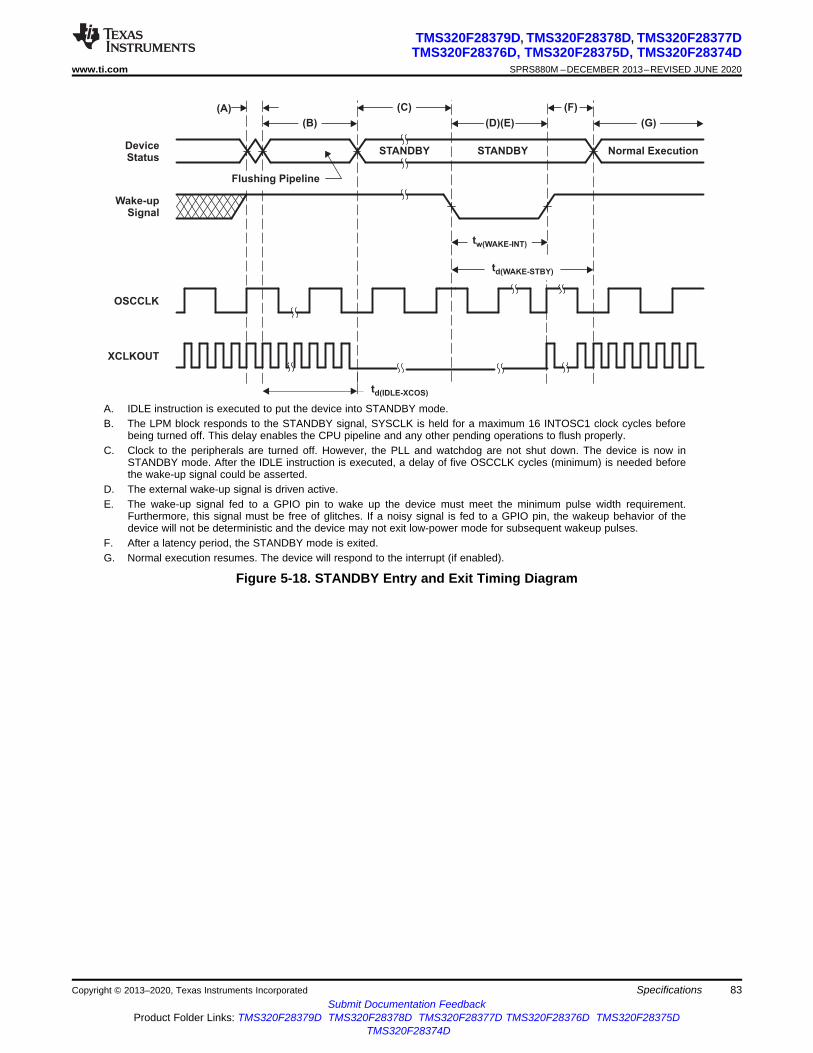
Wake-upSignal
OSCCLK
XCLKOUT
Flushing Pipeline
(A)
DeviceStatus
STANDBY Normal ExecutionSTANDBY
(G)(B)
(C)
(D)(E)
(F)
td(IDLE-XCOS)
tw(WAKE-INT)
td(WAKE-STBY)
83
TMS320F28379D, TMS320F28378D, TMS320F28377DTMS320F28376D, TMS320F28375D, TMS320F28374D
www.ti.com SPRS880M –DECEMBER 2013–REVISED JUNE 2020
Submit Documentation FeedbackProduct Folder Links: TMS320F28379D TMS320F28378D TMS320F28377D TMS320F28376D TMS320F28375D
TMS320F28374D
SpecificationsCopyright © 2013–2020, Texas Instruments Incorporated
A. IDLE instruction is executed to put the device into STANDBY mode.B. The LPM block responds to the STANDBY signal, SYSCLK is held for a maximum 16 INTOSC1 clock cycles before
being turned off. This delay enables the CPU pipeline and any other pending operations to flush properly.C. Clock to the peripherals are turned off. However, the PLL and watchdog are not shut down. The device is now in
STANDBY mode. After the IDLE instruction is executed, a delay of five OSCCLK cycles (minimum) is needed beforethe wake-up signal could be asserted.
D. The external wake-up signal is driven active.E. The wake-up signal fed to a GPIO pin to wake up the device must meet the minimum pulse width requirement.
Furthermore, this signal must be free of glitches. If a noisy signal is fed to a GPIO pin, the wakeup behavior of thedevice will not be deterministic and the device may not exit low-power mode for subsequent wakeup pulses.
F. After a latency period, the STANDBY mode is exited.G. Normal execution resumes. The device will respond to the interrupt (if enabled).
Figure 5-18. STANDBY Entry and Exit Timing Diagram
84
TMS320F28379D, TMS320F28378D, TMS320F28377DTMS320F28376D, TMS320F28375D, TMS320F28374DSPRS880M –DECEMBER 2013–REVISED JUNE 2020 www.ti.com
Submit Documentation FeedbackProduct Folder Links: TMS320F28379D TMS320F28378D TMS320F28377D TMS320F28376D TMS320F28375D
TMS320F28374D
Specifications Copyright © 2013–2020, Texas Instruments Incorporated
Table 5-33 shows the HALT mode timing requirements, Table 5-34 shows the switching characteristics,and Figure 5-19 shows the timing diagram for HALT mode.
(1) For applications using X1/X2 for OSCCLK, the user must characterize their specific oscillator start-up time as it is dependent oncircuit/layout external to the device. See Table 5-17 for more information. For applications using INTOSC1 or INTOSC2 for OSCCLK,see Section 5.9.3.5 for toscst. Oscillator start-up time does not apply to applications using a single-ended crystal on the X1 pin, as it ispowered externally to the device.
Table 5-33. HALT Mode Timing RequirementsMIN MAX UNIT
tw(WAKE-GPIO) Pulse duration, GPIO wake-up signal (1) toscst + 2tc(OSCCLK) cyclestw(WAKE-XRS) Pulse duration, XRS wake-up signal (1) toscst + 8tc(OSCCLK) cycles
(1) This value is based on the flash power-up time, which is a function of the SYSCLK frequency, flash wait states (RWAIT), andFPAC1[PSLEEP]. For more information, see the Flash and OTP Power-Down Modes and Wakeup section of the TMS320F2837xDDual-Core Microcontrollers Technical Reference Manual. This value can be realized when SYSCLK is 200 MHz, RWAIT is 3, andFPAC1[PSLEEP] is 0x860.
Table 5-34. HALT Mode Switching Characteristicsover recommended operating conditions (unless otherwise noted)
PARAMETER MIN MAX UNITtd(IDLE-XCOS) Delay time, IDLE instruction executed to XCLKOUT stop 16tc(INTOSC1) cycles
td(WAKE-HALT)
Delay time, external wake signal end to CPU1 programexecution resume
cycles
• Wakeup from flash– Flash module in active state
75tc(OSCCLK)
• Wakeup from flash– Flash module in sleep state
17500tc(OSCCLK)(1)
• Wakeup from RAM 75tc(OSCCLK)
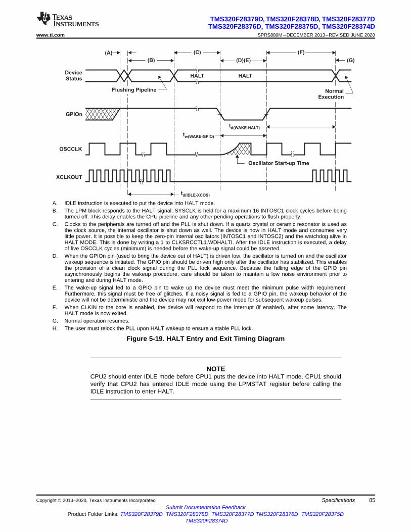
OSCCLK
XCLKOUT
HALT HALT
Flushing Pipeline
DeviceStatus
NormalExecution
GPIOn
(A) (C)
(D)(E)
(F)
(B) (G)
td(IDLE-XCOS)
tw(WAKE-GPIO)
td(WAKE-HALT)
Oscillator Start-up Time
85
TMS320F28379D, TMS320F28378D, TMS320F28377DTMS320F28376D, TMS320F28375D, TMS320F28374D
www.ti.com SPRS880M –DECEMBER 2013–REVISED JUNE 2020
Submit Documentation FeedbackProduct Folder Links: TMS320F28379D TMS320F28378D TMS320F28377D TMS320F28376D TMS320F28375D
TMS320F28374D
SpecificationsCopyright © 2013–2020, Texas Instruments Incorporated
A. IDLE instruction is executed to put the device into HALT mode.B. The LPM block responds to the HALT signal, SYSCLK is held for a maximum 16 INTOSC1 clock cycles before being
turned off. This delay enables the CPU pipeline and any other pending operations to flush properly.C. Clocks to the peripherals are turned off and the PLL is shut down. If a quartz crystal or ceramic resonator is used as
the clock source, the internal oscillator is shut down as well. The device is now in HALT mode and consumes verylittle power. It is possible to keep the zero-pin internal oscillators (INTOSC1 and INTOSC2) and the watchdog alive inHALT MODE. This is done by writing a 1 to CLKSRCCTL1.WDHALTI. After the IDLE instruction is executed, a delayof five OSCCLK cycles (minimum) is needed before the wake-up signal could be asserted.
D. When the GPIOn pin (used to bring the device out of HALT) is driven low, the oscillator is turned on and the oscillatorwakeup sequence is initiated. The GPIO pin should be driven high only after the oscillator has stabilized. This enablesthe provision of a clean clock signal during the PLL lock sequence. Because the falling edge of the GPIO pinasynchronously begins the wakeup procedure, care should be taken to maintain a low noise environment prior toentering and during HALT mode.
E. The wake-up signal fed to a GPIO pin to wake up the device must meet the minimum pulse width requirement.Furthermore, this signal must be free of glitches. If a noisy signal is fed to a GPIO pin, the wakeup behavior of thedevice will not be deterministic and the device may not exit low-power mode for subsequent wakeup pulses.
F. When CLKIN to the core is enabled, the device will respond to the interrupt (if enabled), after some latency. TheHALT mode is now exited.
G. Normal operation resumes.H. The user must relock the PLL upon HALT wakeup to ensure a stable PLL lock.
Figure 5-19. HALT Entry and Exit Timing Diagram
NOTECPU2 should enter IDLE mode before CPU1 puts the device into HALT mode. CPU1 shouldverify that CPU2 has entered IDLE mode using the LPMSTAT register before calling theIDLE instruction to enter HALT.
86
TMS320F28379D, TMS320F28378D, TMS320F28377DTMS320F28376D, TMS320F28375D, TMS320F28374DSPRS880M –DECEMBER 2013–REVISED JUNE 2020 www.ti.com
Submit Documentation FeedbackProduct Folder Links: TMS320F28379D TMS320F28378D TMS320F28377D TMS320F28376D TMS320F28375D
TMS320F28374D
Specifications Copyright © 2013–2020, Texas Instruments Incorporated
Table 5-35 shows the HIBERNATE mode timing requirements, Table 5-36 shows the switchingcharacteristics, and Figure 5-20 shows the timing diagram for HIBERNATE mode.
Table 5-35. HIBERNATE Mode Timing RequirementsMIN MAX UNIT
tw(HIBWAKE) Pulse duration, HIBWAKE signal 40 µstw(WAKEXRS) Pulse duration, XRS wake-up signal 40 µs
Table 5-36. HIBERNATE Mode Switching Characteristicsover recommended operating conditions (unless otherwise noted)
PARAMETER MIN MAX UNITtd(IDLE-XCOS) Delay time, IDLE instruction executed to XCLKOUT stop 30tc(SYSCLK) cyclestd(WAKE-HIB) Delay time, external wake signal to lORestore function start 1.5 ms
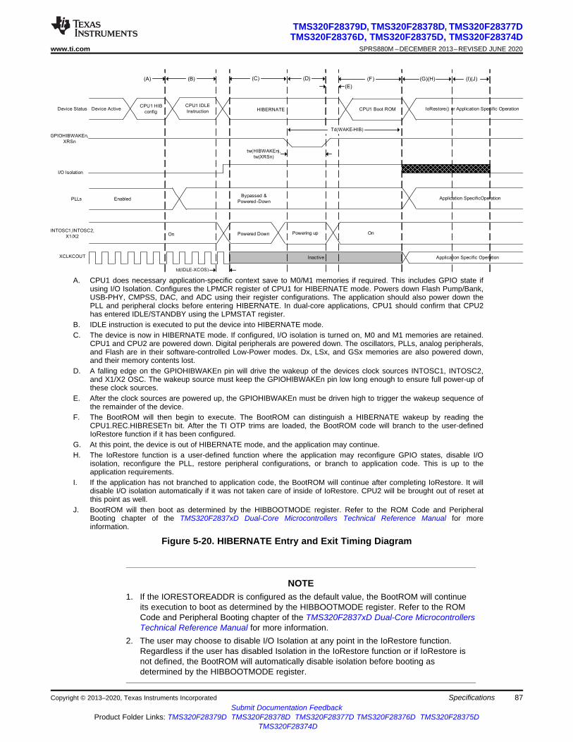
Inactive
Device ActiveCPU1 IDLE
Instruction
EnabledBypassed &
Powered -Down
On Powered Down Powering up On
HIBERNATE CPU1 Boot ROMDevice Status
INTOSC1,INTOSC2,
X1/X2
GPIOHIBWAKEn,
XRSn
PLLs
I/O Isolation
IoRestore() or Application Specific OperationCPU1 HIB
config
(A) (B) (C) (D)
tw(HIBWAKEn),
tw(XRSn)
(F) (G)(H) (I)(J)
XCLKCOUT Application Specific Operation
Application SpecificOperation
(E)
td(IDLE-XCOS)
Td(WAKE-HIB)
87
TMS320F28379D, TMS320F28378D, TMS320F28377DTMS320F28376D, TMS320F28375D, TMS320F28374D
www.ti.com SPRS880M –DECEMBER 2013–REVISED JUNE 2020
Submit Documentation FeedbackProduct Folder Links: TMS320F28379D TMS320F28378D TMS320F28377D TMS320F28376D TMS320F28375D
TMS320F28374D
SpecificationsCopyright © 2013–2020, Texas Instruments Incorporated
A. CPU1 does necessary application-specific context save to M0/M1 memories if required. This includes GPIO state ifusing I/O Isolation. Configures the LPMCR register of CPU1 for HIBERNATE mode. Powers down Flash Pump/Bank,USB-PHY, CMPSS, DAC, and ADC using their register configurations. The application should also power down thePLL and peripheral clocks before entering HIBERNATE. In dual-core applications, CPU1 should confirm that CPU2has entered IDLE/STANDBY using the LPMSTAT register.
B. IDLE instruction is executed to put the device into HIBERNATE mode.C. The device is now in HIBERNATE mode. If configured, I/O isolation is turned on, M0 and M1 memories are retained.
CPU1 and CPU2 are powered down. Digital peripherals are powered down. The oscillators, PLLs, analog peripherals,and Flash are in their software-controlled Low-Power modes. Dx, LSx, and GSx memories are also powered down,and their memory contents lost.
D. A falling edge on the GPIOHIBWAKEn pin will drive the wakeup of the devices clock sources INTOSC1, INTOSC2,and X1/X2 OSC. The wakeup source must keep the GPIOHIBWAKEn pin low long enough to ensure full power-up ofthese clock sources.
E. After the clock sources are powered up, the GPIOHIBWAKEn must be driven high to trigger the wakeup sequence ofthe remainder of the device.
F. The BootROM will then begin to execute. The BootROM can distinguish a HIBERNATE wakeup by reading theCPU1.REC.HIBRESETn bit. After the TI OTP trims are loaded, the BootROM code will branch to the user-definedIoRestore function if it has been configured.
G. At this point, the device is out of HIBERNATE mode, and the application may continue.H. The IoRestore function is a user-defined function where the application may reconfigure GPIO states, disable I/O
isolation, reconfigure the PLL, restore peripheral configurations, or branch to application code. This is up to theapplication requirements.
I. If the application has not branched to application code, the BootROM will continue after completing IoRestore. It willdisable I/O isolation automatically if it was not taken care of inside of IoRestore. CPU2 will be brought out of reset atthis point as well.
J. BootROM will then boot as determined by the HIBBOOTMODE register. Refer to the ROM Code and PeripheralBooting chapter of the TMS320F2837xD Dual-Core Microcontrollers Technical Reference Manual for moreinformation.
Figure 5-20. HIBERNATE Entry and Exit Timing Diagram
NOTE1. If the IORESTOREADDR is configured as the default value, the BootROM will continue
its execution to boot as determined by the HIBBOOTMODE register. Refer to the ROMCode and Peripheral Booting chapter of the TMS320F2837xD Dual-Core MicrocontrollersTechnical Reference Manual for more information.
2. The user may choose to disable I/O Isolation at any point in the IoRestore function.Regardless if the user has disabled Isolation in the IoRestore function or if IoRestore isnot defined, the BootROM will automatically disable isolation before booting asdetermined by the HIBBOOTMODE register.
88
TMS320F28379D, TMS320F28378D, TMS320F28377DTMS320F28376D, TMS320F28375D, TMS320F28374DSPRS880M –DECEMBER 2013–REVISED JUNE 2020 www.ti.com
Submit Documentation FeedbackProduct Folder Links: TMS320F28379D TMS320F28378D TMS320F28377D TMS320F28376D TMS320F28375D
TMS320F28374D
Specifications Copyright © 2013–2020, Texas Instruments Incorporated
NOTEFor applications using both CPU1 and CPU2, TI recommends that the application puts CPU2in either IDLE or STANDBY before entering HIBERNATE mode. If any GPIOs are used andthe state is to be preserved, data can be stored in M0/M1 memory of CPU1 to bereconfigured upon wakeup. This should be done before step A of Figure 5-20.
89
TMS320F28379D, TMS320F28378D, TMS320F28377DTMS320F28376D, TMS320F28375D, TMS320F28374D
www.ti.com SPRS880M –DECEMBER 2013–REVISED JUNE 2020
Submit Documentation FeedbackProduct Folder Links: TMS320F28379D TMS320F28378D TMS320F28377D TMS320F28376D TMS320F28375D
TMS320F28374D
SpecificationsCopyright © 2013–2020, Texas Instruments Incorporated
5.9.9 External Memory Interface (EMIF)The EMIF provides a means of connecting the CPU to various external storage devices like asynchronousmemories (SRAM, NOR flash) or synchronous memory (SDRAM).
5.9.9.1 Asynchronous Memory Support
The EMIF supports asynchronous memories:• SRAMs• NOR Flash memories
There is an external wait input that allows slower asynchronous memories to extend the memory access.The EMIF module supports up to three chip selects (EMIF_CS[4:2]). Each chip select has the followingindividually programmable attributes:• Data bus width• Read cycle timings: setup, hold, strobe• Write cycle timings: setup, hold, strobe• Bus turnaround time• Extended wait option with programmable time-out• Select strobe option
5.9.9.2 Synchronous DRAM Support
The EMIF memory controller is compliant with the JESD21-C SDR SDRAMs that use a 32-bit or 16-bitdata bus. The EMIF has a single SDRAM chip select (EMIF_CS[0]).
The address space of the EMIF, for the synchronous memory (SDRAM), lies beyond the 22-bit range ofthe program address bus and can only be accessed through the data bus, which places a restriction onthe C compiler being able to work effectively on data in this space. Therefore, when using SDRAM, theuser is advised to copy data (using the DMA) from external memory to RAM before working on it. See theexamples in C2000Ware (C2000Ware for C2000 MCUs) and the TMS320F2837xD Dual-CoreMicrocontrollers Technical Reference Manual.
SDRAM configurations supported are:• One-bank, two-bank, and four-bank SDRAM devices• Devices with 8-, 9-, 10-, and 11-column addresses• CAS latency of two or three clock cycles• 16-bit/32-bit data bus width• 3.3-V LVCMOS interface
Additionally, the EMIF supports placing the SDRAM in self-refresh and power-down modes. Self-refreshmode allows the SDRAM to be put in a low-power state while still retaining memory contents because theSDRAM will continue to refresh itself even without clocks from the microcontroller. Power-down modeachieves even lower power, except the microcontroller must periodically wake up and issue refreshes ifdata retention is required. The EMIF module does not support mobile SDRAM devices.
On this device, the EMIF does not support burst access for SDRAM configurations. This means everyaccess to an external SDRAM device will have CAS latency.
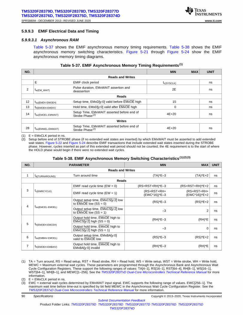
90
TMS320F28379D, TMS320F28378D, TMS320F28377DTMS320F28376D, TMS320F28375D, TMS320F28374DSPRS880M –DECEMBER 2013–REVISED JUNE 2020 www.ti.com
Submit Documentation FeedbackProduct Folder Links: TMS320F28379D TMS320F28378D TMS320F28377D TMS320F28376D TMS320F28375D
TMS320F28374D
Specifications Copyright © 2013–2020, Texas Instruments Incorporated
5.9.9.3 EMIF Electrical Data and Timing
5.9.9.3.1 Asynchronous RAM
Table 5-37 shows the EMIF asynchronous memory timing requirements. Table 5-38 shows the EMIFasynchronous memory switching characteristics. Figure 5-21 through Figure 5-24 show the EMIFasynchronous memory timing diagrams.
(1) E = EMxCLK period in ns.(2) Setup before end of STROBE phase (if no extended wait states are inserted) by which EMxWAIT must be asserted to add extended
wait states. Figure 5-22 and Figure 5-24 describe EMIF transactions that include extended wait states inserted during the STROBEphase. However, cycles inserted as part of this extended wait period should not be counted; the 4E requirement is to the start of wherethe HOLD phase would begin if there were no extended wait cycles.
Table 5-37. EMIF Asynchronous Memory Timing Requirements (1)
NO. MIN MAX UNITReads and Writes
E EMIF clock period tc(SYSCLK) ns
2 tw(EM_WAIT)Pulse duration, EMxWAIT assertion anddeassertion 2E ns
Reads12 tsu(EMDV-EMOEH) Setup time, EMxD[y:0] valid before EMxOE high 15 ns13 th(EMOEH-EMDIV) Hold time, EMxD[y:0] valid after EMxOE high 0 ns
14 tsu(EMOEL-EMWAIT)Setup Time, EMxWAIT asserted before end ofStrobe Phase (2) 4E+20 ns
Writes
28 tsu(EMWEL-EMWAIT)Setup Time, EMxWAIT asserted before end ofStrobe Phase (2) 4E+20 ns
(1) TA = Turn around, RS = Read setup, RST = Read strobe, RH = Read hold, WS = Write setup, WST = Write strobe, WH = Write hold,MEWC = Maximum external wait cycles. These parameters are programmed through the Asynchronous Bank and Asynchronous WaitCycle Configuration Registers. These support the following ranges of values: TA[4–1], RS[16–1], RST[64–4], RH[8–1], WS[16–1],WST[64–1], WH[8–1], and MEWC[1–256]. See the TMS320F2837xD Dual-Core Microcontrollers Technical Reference Manual for moreinformation.
(2) E = EMxCLK period in ns.(3) EWC = external wait cycles determined by EMxWAIT input signal. EWC supports the following range of values. EWC[256–1]. The
maximum wait time before time-out is specified by bit field MEWC in the Asynchronous Wait Cycle Configuration Register. See theTMS320F2837xD Dual-Core Microcontrollers Technical Reference Manual for more information.
Table 5-38. EMIF Asynchronous Memory Switching Characteristics (1) (2) (3)
NO. PARAMETER MIN MAX UNITReads and Writes
1 td(TURNAROUND) Turn around time (TA)*E–3 (TA)*E+2 nsReads
3 tc(EMRCYCLE)
EMIF read cycle time (EW = 0) (RS+RST+RH)*E–3 (RS+RST+RH)*E+2 ns
EMIF read cycle time (EW = 1) (RS+RST+RH+(EWC*16))*E–3
(RS+RST+RH+(EWC*16))*E+2 ns
4 tsu(EMCEL-EMOEL)
Output setup time, EMxCS[y:2] lowto EMxOE low (SS = 0) (RS)*E–3 (RS)*E+2 ns
Output setup time, EMxCS[y:2] lowto EMxOE low (SS = 1) –3 2 ns
5 th(EMOEH-EMCEH)
Output hold time, EMxOE high toEMxCS[y:2] high (SS = 0) (RH)*E–3 (RH)*E ns
Output hold time, EMxOE high toEMxCS[y:2] high (SS = 1) –3 0 ns
6 tsu(EMBAV-EMOEL)Output setup time, EMxBA[y:0]valid to EMxOE low (RS)*E–3 (RS)*E+2 ns
7 th(EMOEH-EMBAIV)Output hold time, EMxOE high toEMxBA[y:0] invalid (RH)*E–3 (RH)*E ns
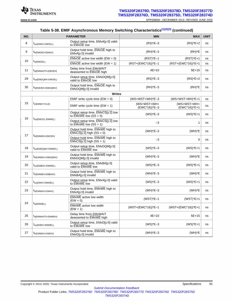
91
TMS320F28379D, TMS320F28378D, TMS320F28377DTMS320F28376D, TMS320F28375D, TMS320F28374D
www.ti.com SPRS880M –DECEMBER 2013–REVISED JUNE 2020
Submit Documentation FeedbackProduct Folder Links: TMS320F28379D TMS320F28378D TMS320F28377D TMS320F28376D TMS320F28375D
TMS320F28374D
SpecificationsCopyright © 2013–2020, Texas Instruments Incorporated
Table 5-38. EMIF Asynchronous Memory Switching Characteristics(1)(2)(3) (continued)NO. PARAMETER MIN MAX UNIT
8 tsu(EMAV-EMOEL)Output setup time, EMxA[y:0] validto EMxOE low (RS)*E–3 (RS)*E+2 ns
9 th(EMOEH-EMAIV)Output hold time, EMxOE high toEMxA[y:0] invalid (RH)*E–3 (RH)*E ns
10 tw(EMOEL)EMxOE active low width (EW = 0) (RST)*E–1 (RST)*E+1 nsEMxOE active low width (EW = 1) (RST+(EWC*16))*E–1 (RST+(EWC*16))*E+1 ns
11 td(EMWAITH-EMOEH)Delay time from EMxWAITdeasserted to EMxOE high 4E+10 5E+15 ns
29 tsu(EMDQMV-EMOEL)Output setup time, EMxDQM[y:0]valid to EMxOE low (RS)*E–3 (RS)*E+2 ns
30 th(EMOEH-EMDQMIV)Output hold time, EMxOE high toEMxDQM[y:0] invalid (RH)*E–3 (RH)*E ns
Writes
15 tc(EMWCYCLE)
EMIF write cycle time (EW = 0) (WS+WST+WH)*E–3 (WS+WST+WH)*E+1 ns
EMIF write cycle time (EW = 1) (WS+WST+WH+(EWC*16))*E–3
(WS+WST+WH+(EWC*16))*E+1 ns
16 tsu(EMCEL-EMWEL)
Output setup time, EMxCS[y:2] lowto EMxWE low (SS = 0) (WS)*E–3 (WS)*E+1 ns
Output setup time, EMxCS[y:2] lowto EMxWE low (SS = 1) –3 1 ns
17 th(EMWEH-EMCEH)
Output hold time, EMxWE high toEMxCS[y:2] high (SS = 0) (WH)*E–3 (WH)*E ns
Output hold time, EMxWE high toEMxCS[y:2] high (SS = 1) –3 0 ns
18 tsu(EMDQMV-EMWEL)Output setup time, EMxDQM[y:0]valid to EMxWE low (WS)*E–3 (WS)*E+1 ns
19 th(EMWEH-EMDQMIV)Output hold time, EMxWE high toEMxDQM[y:0] invalid (WH)*E–3 (WH)*E ns
20 tsu(EMBAV-EMWEL)Output setup time, EMxBA[y:0]valid to EMxWE low (WS)*E–3 (WS)*E+1 ns
21 th(EMWEH-EMBAIV)Output hold time, EMxWE high toEMxBA[y:0] invalid (WH)*E–3 (WH)*E ns
22 tsu(EMAV-EMWEL)Output setup time, EMxA[y:0] validto EMxWE low (WS)*E–3 (WS)*E+1 ns
23 th(EMWEH-EMAIV)Output hold time, EMxWE high toEMxA[y:0] invalid (WH)*E–3 (WH)*E ns
24 tw(EMWEL)
EMxWE active low width(EW = 0) (WST)*E–1 (WST)*E+1 ns
EMxWE active low width(EW = 1) (WST+(EWC*16))*E–1 (WST+(EWC*16))*E+1 ns
25 td(EMWAITH-EMWEH)Delay time from EMxWAITdeasserted to EMxWE high 4E+10 5E+15 ns
26 tsu(EMDV-EMWEL)Output setup time, EMxD[y:0] validto EMxWE low (WS)*E–3 (WS)*E+1 ns
27 th(EMWEH-EMDIV)Output hold time, EMxWE high toEMxD[y:0] invalid (WH)*E–3 (WH)*E ns

11
Asserted Deasserted
22
EMxWAIT
SETUP Extended Due to EMxWAIT STROBE HOLD
14
STROBE
EMxCS[y:2]
EMxBA[y:0]
EMxA[y:0]
EMxOE
EMxD[y:0]
EMxCS[y:2]
EMxBA[y:0]
13
12
EMxA[y:0]
EMxOE
EMxD[y:0]
EMxWE
10
5
9
7
4
8
6
3
1
EMxDQM[y:0]
3029
92
TMS320F28379D, TMS320F28378D, TMS320F28377DTMS320F28376D, TMS320F28375D, TMS320F28374DSPRS880M –DECEMBER 2013–REVISED JUNE 2020 www.ti.com
Submit Documentation FeedbackProduct Folder Links: TMS320F28379D TMS320F28378D TMS320F28377D TMS320F28376D TMS320F28375D
TMS320F28374D
Specifications Copyright © 2013–2020, Texas Instruments Incorporated
Figure 5-21. Asynchronous Memory Read Timing
Figure 5-22. EMxWAIT Read Timing Requirements
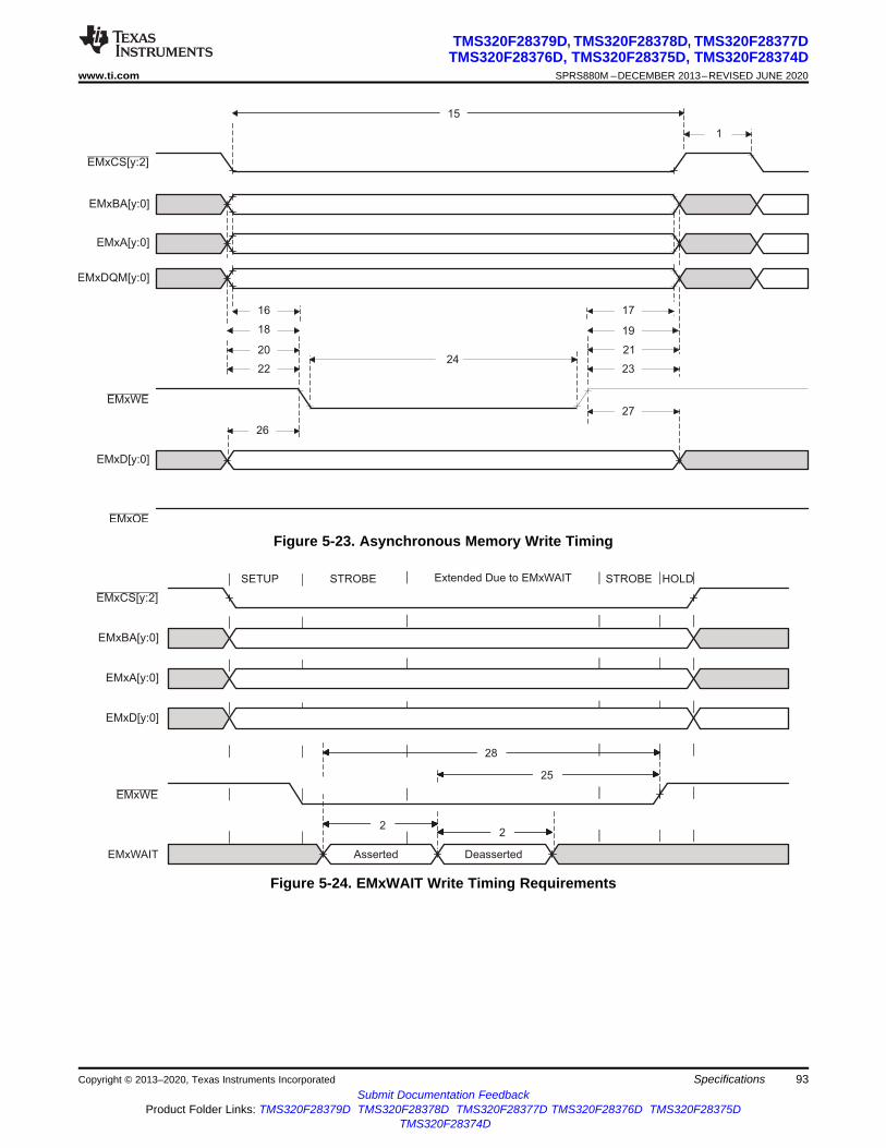
25
Asserted
22
EMxWAIT
SETUP Extended Due to EMxWAIT
28
Deasserted
STROBE STROBE HOLD
EMxCS[y:2]
EMxBA[y:0]
EMxA[y:0]
EMxD[y:0]
EMxWE
15
1
16
18
20
2224
17
19
21
23
26
27
EMxCS[y:2]
EMxBA[y:0]
EMxA[y:0]
EMxOE
EMxD[y:0]
EMxWE
EMxDQM[y:0]
93
TMS320F28379D, TMS320F28378D, TMS320F28377DTMS320F28376D, TMS320F28375D, TMS320F28374D
www.ti.com SPRS880M –DECEMBER 2013–REVISED JUNE 2020
Submit Documentation FeedbackProduct Folder Links: TMS320F28379D TMS320F28378D TMS320F28377D TMS320F28376D TMS320F28375D
TMS320F28374D
SpecificationsCopyright © 2013–2020, Texas Instruments Incorporated
Figure 5-23. Asynchronous Memory Write Timing
Figure 5-24. EMxWAIT Write Timing Requirements
94
TMS320F28379D, TMS320F28378D, TMS320F28377DTMS320F28376D, TMS320F28375D, TMS320F28374DSPRS880M –DECEMBER 2013–REVISED JUNE 2020 www.ti.com
Submit Documentation FeedbackProduct Folder Links: TMS320F28379D TMS320F28378D TMS320F28377D TMS320F28376D TMS320F28375D
TMS320F28374D
Specifications Copyright © 2013–2020, Texas Instruments Incorporated
5.9.9.3.2 Synchronous RAM
Table 5-39 shows the EMIF synchronous memory timing requirements. Table 5-40 shows the EMIFsynchronous memory switching characteristics. Figure 5-25 and Figure 5-26 show the synchronousmemory timing diagrams.
Table 5-39. EMIF Synchronous Memory Timing RequirementsNO. MIN MAX UNIT19 tsu(EMIFDV-EM_CLKH) Input setup time, read data valid on EMxD[y:0] before EMxCLK rising 2 ns20 th(CLKH-DIV) Input hold time, read data valid on EMxD[y:0] after EMxCLK rising 1.5 ns
Table 5-40. EMIF Synchronous Memory Switching CharacteristicsNO. PARAMETER MIN MAX UNIT
1 tc(CLK) Cycle time, EMIF clock EMxCLK 10 ns2 tw(CLK) Pulse width, EMIF clock EMxCLK high or low 3 ns3 td(CLKH-CSV) Delay time, EMxCLK rising to EMxCS[y:2] valid 8 ns4 toh(CLKH-CSIV) Output hold time, EMxCLK rising to EMxCS[y:2] invalid 1 ns5 td(CLKH-DQMV) Delay time, EMxCLK rising to EMxDQM[y:0] valid 8 ns6 toh(CLKH-DQMIV) Output hold time, EMxCLK rising to EMxDQM[y:0] invalid 1 ns7 td(CLKH-AV) Delay time, EMxCLK rising to EMxA[y:0] and EMxBA[y:0] valid 8 ns8 toh(CLKH-AIV) Output hold time, EMxCLK rising to EMxA[y:0] and EMxBA[y:0] invalid 1 ns9 td(CLKH-DV) Delay time, EMxCLK rising to EMxD[y:0] valid 8 ns10 toh(CLKH-DIV) Output hold time, EMxCLK rising to EMxD[y:0] invalid 1 ns11 td(CLKH-RASV) Delay time, EMxCLK rising to EMxRAS valid 8 ns12 toh(CLKH-RASIV) Output hold time, EMxCLK rising to EMxRAS invalid 1 ns13 td(CLKH-CASV) Delay time, EMxCLK rising to EMxCAS valid 8 ns14 toh(CLKH-CASIV) Output hold time, EMxCLK rising to EMxCAS invalid 1 ns15 td(CLKH-WEV) Delay time, EMxCLK rising to EMxWE valid 8 ns16 toh(CLKH-WEIV) Output hold time, EMxCLK rising to EMxWE invalid 1 ns17 td(CLKH-DHZ) Delay time, EMxCLK rising to EMxD[y:0] tri-stated 8 ns18 toh(CLKH-DLZ) Output hold time, EMxCLK rising to EMxD[y:0] driving 1 ns

EMxCLK
1
2 2
4
6
8
8
12
14
19
20
3
5
7
7
11
13
17 182 EM_CLK Delay
BASIC SDRAM
READ OPERATION
EMxRAS
EMxCAS
EMxCS[y:2]
EMxBA[y:0]
EMxA[y:0]
EMxD[y:0]
EMxWE
EMxDQM[y:0]
95
TMS320F28379D, TMS320F28378D, TMS320F28377DTMS320F28376D, TMS320F28375D, TMS320F28374D
www.ti.com SPRS880M –DECEMBER 2013–REVISED JUNE 2020
Submit Documentation FeedbackProduct Folder Links: TMS320F28379D TMS320F28378D TMS320F28377D TMS320F28376D TMS320F28375D
TMS320F28374D
SpecificationsCopyright © 2013–2020, Texas Instruments Incorporated
Figure 5-25. Basic SDRAM Read Operation
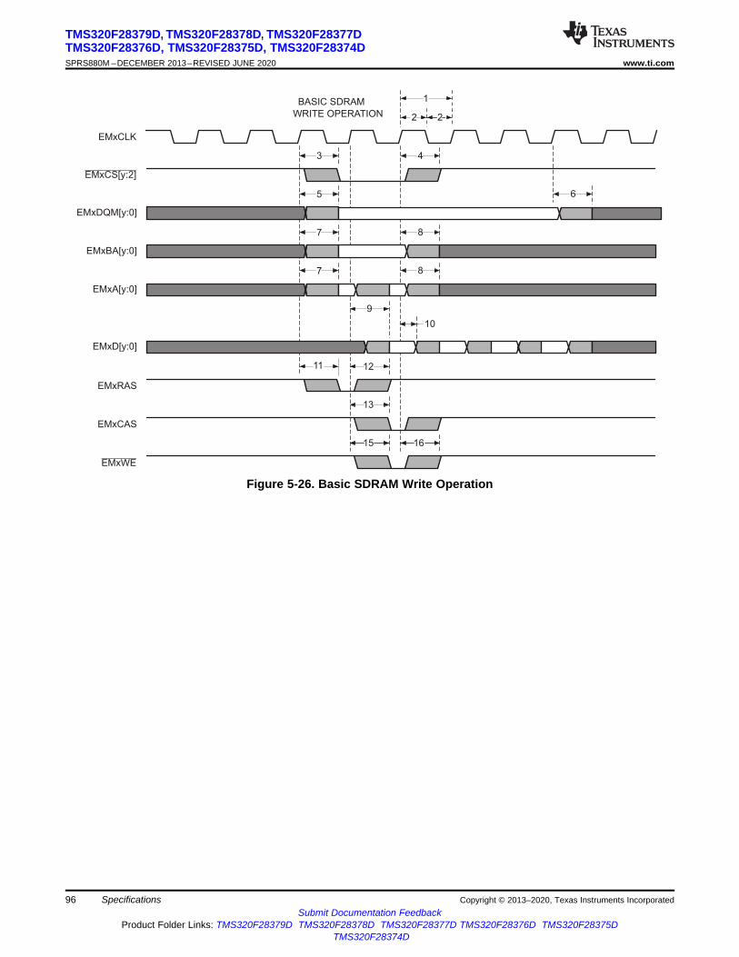
EMxCLK
1
2 2
4
6
8
8
12
10
16
3
5
7
7
11
13
15
9
BASIC SDRAM
WRITE OPERATION
EMxRAS
EMxCAS
EMxCS[y:2]
EMxBA[y:0]
EMxA[y:0]
EMxD[y:0]
EMxWE
EMxDQM[y:0]
96
TMS320F28379D, TMS320F28378D, TMS320F28377DTMS320F28376D, TMS320F28375D, TMS320F28374DSPRS880M –DECEMBER 2013–REVISED JUNE 2020 www.ti.com
Submit Documentation FeedbackProduct Folder Links: TMS320F28379D TMS320F28378D TMS320F28377D TMS320F28376D TMS320F28375D
TMS320F28374D
Specifications Copyright © 2013–2020, Texas Instruments Incorporated
Figure 5-26. Basic SDRAM Write Operation
97
TMS320F28379D, TMS320F28378D, TMS320F28377DTMS320F28376D, TMS320F28375D, TMS320F28374D
www.ti.com SPRS880M –DECEMBER 2013–REVISED JUNE 2020
Submit Documentation FeedbackProduct Folder Links: TMS320F28379D TMS320F28378D TMS320F28377D TMS320F28376D TMS320F28375D
TMS320F28374D
SpecificationsCopyright © 2013–2020, Texas Instruments Incorporated
5.10 Analog PeripheralsThe analog subsystem module is described in this section.
The analog modules on this device include the ADC, temperature sensor, buffered DAC, and CMPSS.
The analog subsystem has the following features:• Flexible voltage references
– The ADCs are referenced to VREFHIx and VREFLOx pins.• VREFHIx pin voltage must be driven in externally.
• The buffered DACs are referenced to VREFHIx and VSSA.– Alternately, these DACs can be referenced to the VDAC pin and VSSA.
• The comparator DACs are referenced to VDDA and VSSA.– Alternately, these DACs can be referenced to the VDAC pin and VSSA.
• Flexible pin usage– Buffered DAC and comparator subsystem functions multiplexed with ADC inputs
• Internal connection to VREFLO on all ADCs for offset self-calibration
Figure 5-27 shows the Analog Subsystem Block Diagram for the 337-ball ZWT package. Figure 5-28shows the Analog Subsystem Block Diagram for the 176-pin PTP package. Figure 5-29 shows the AnalogSubsystem Block Diagram for the 100-pin PZP package.

ADC-A
16-bits
or
12-bits
(selectable)
0123456789
101112131415
ADC-B
16-bits
or
12-bits
(selectable)
ADC-C
16-bits
or
12-bits
(selectable)
ADC-D
16-bits
or
12-bits
(selectable)
DACOUTA/ADCINA0DACOUTB/ADCINA1CMPIN1P/ADCINA2CMPIN1N/ADCINA3
CMPIN4N/ADCIN15
TEMP SENSOR
VDAC/ADCINB0DACOUTC/ADCINB1CMPIN3P/ADCINB2CMPIN3N/ADCINB3
CMPIN6P/ADCINC2CMPIN6N/ADCINC3
CMPIN7P/ADCIND0CMPIN7N/ADCIND1CMPIN8P/ADCIND2CMPIN8N/ADCIND3
12-bit
Buffered
DAC
CMPIN2P/ADCINA4CMPIN2N/ADCINA5
ADCINB4ADCINB5
CMPIN5P/ADCINC4CMPIN5N/ADCINC5
ADCIND4ADCIND5
VREFHIA
VREFLOB
REFHIVREFHIA
DA
CO
UT
AD
AC
OU
TB
VREFLOC
VREFLOD
VREFLOBVREFLOB
VDAC
0123456789
101112131415
0123456789
101112131415
0123456789
101112131415
VREFLODVREFLOD
VREFLOCVREFLOC
VREFLOAVREFLOA
CMPIN4P/ADCIN14
CMPIN1P
CMPIN3P
CMPIN2P
CMPIN4P
Comparator Subsystem 1
VDDA or VDAC
CMPIN1N
CTRIPOUT1H
Digital
Filter
CTRIP1H
CTRIP1L
CMPIN2N
CTRIP2L
CTRIP2H
CMPIN3N
CTRIPOUT3H
CTRIP3H
CTRIP3L
CMPIN4N
CTRIPOUT4H
CTRIP4H
CTRIP4L
Digital
Filter CTRIPOUT1L
CTRIPOUT2H
CTRIPOUT2L
CTRIPOUT3L
CTRIPOUT4L
CMPIN5P
CMPIN6P
CMPIN5N
CTRIPOUT5H
CTRIP5H
CTRIP5L
CMPIN6N
CTRIPOUT6H
CTRIP6H
CTRIP6L
CTRIPOUT5L
CTRIPOUT6L
CMPIN7P
CMPIN8P
CMPIN7N
CTRIPOUT7H
CTRIP7H
CTRIP7L
CMPIN8N
CTRIPOUT8H
CTRIP8H
CTRIP8L
CTRIPOUT7L
CTRIPOUT8L
12-bit
Buffered
DAC
VREFHIA VDAC
12-bit
Buffered
DAC
VREFHIB
DA
CO
UT
CVDAC
REFHI
DAC12
DAC12
Comparator Subsystem 2
VDDA or VDACDigital
Filter
Digital
Filter
DAC12
DAC12
Comparator Subsystem 3
VDDA or VDACDigital
Filter
Digital
Filter
DAC12
DAC12
Comparator Subsystem 4
VDDA or VDACDigital
Filter
Digital
Filter
DAC12
DAC12
Comparator Subsystem 5
VDDA or VDACDigital
Filter
Digital
Filter
DAC12
DAC12
Comparator Subsystem 6
VDDA or VDACDigital
Filter
Digital
Filter
DAC12
DAC12
Comparator Subsystem 7
VDDA or VDACDigital
Filter
Digital
Filter
DAC12
DAC12
Comparator Subsystem 8
VDDA or VDACDigital
Filter
Digital
Filter
DAC12
DAC12
REFLO
VREFLOA
VREFHIB
REFLO
VREFHIC
VREFHID
REFHI
REFLO
REFHI
REFLO
VSSA
VSSA
VSSA
DACREFSEL
DACREFSEL
DACREFSEL
98
TMS320F28379D, TMS320F28378D, TMS320F28377DTMS320F28376D, TMS320F28375D, TMS320F28374DSPRS880M –DECEMBER 2013–REVISED JUNE 2020 www.ti.com
Submit Documentation FeedbackProduct Folder Links: TMS320F28379D TMS320F28378D TMS320F28377D TMS320F28376D TMS320F28375D
TMS320F28374D
Specifications Copyright © 2013–2020, Texas Instruments Incorporated
Figure 5-27. Analog Subsystem Block Diagram (337-Ball ZWT)

ADC-A
16-bits
or
12-bits
(selectable)
0123456789
101112131415
ADC-B
16-bits
or
12-bits
(selectable)
ADC-D
16-bits
or
12-bits
(selectable)
DACOUTA/ADCINA0DACOUTB/ADCINA1CMPIN1P/ADCINA2CMPIN1N/ADCINA3
CMPIN4N/ADCIN15
TEMP SENSOR
VDAC/ADCINB0DACOUTC/ADCINB1CMPIN3P/ADCINB2CMPIN3N/ADCINB3
CMPIN7P/ADCIND0CMPIN7N/ADCIND1CMPIN8P/ADCIND2CMPIN8N/ADCIND3
12-bit
Buffered
DAC
CMPIN2P/ADCINA4CMPIN2N/ADCINA5
ADCIND4
VREFHIA
VREFLOB
REFHIVREFHIA
DA
CO
UT
AD
AC
OU
TB
VREFLOD
VREFLOBVREFLOB
VDAC
0123456789
101112131415
0123456789
101112131415
VREFLODVREFLOD
VREFLOAVREFLOA
CMPIN4P/ADCIN14
CMPIN1P
CMPIN3P
CMPIN2P
CMPIN4P
Comparator Subsystem 1
VDDA or VDAC
CMPIN1N
CTRIPOUT1H
Digital
Filter
CTRIP1H
CTRIP1L
CMPIN2N
CTRIP2L
CTRIP2H
CMPIN3N
CTRIPOUT3H
CTRIP3H
CTRIP3L
CMPIN4N
CTRIPOUT4H
CTRIP4H
CTRIP4L
Digital
Filter CTRIPOUT1L
CTRIPOUT2H
CTRIPOUT2L
CTRIPOUT3L
CTRIPOUT4L
CMPIN5P
CMPIN6P
CTRIPOUT5H
CTRIP5H
CTRIP5L
CMPIN6N
CTRIPOUT6H
CTRIP6H
CTRIP6L
CTRIPOUT5L
CTRIPOUT6L
CMPIN7P
CMPIN8P
CMPIN7N
CTRIPOUT7H
CTRIP7H
CTRIP7L
CMPIN8N
CTRIPOUT8H
CTRIP8H
CTRIP8L
CTRIPOUT7L
CTRIPOUT8L
12-bit
Buffered
DAC
VREFHIA VDAC
12-bit
Buffered
DAC
VREFHIB
DA
CO
UT
CVDAC
REFHI
DAC12
DAC12
Comparator Subsystem 2
VDDA or VDACDigital
Filter
Digital
Filter
DAC12
DAC12
Comparator Subsystem 3
VDDA or VDACDigital
Filter
Digital
Filter
DAC12
DAC12
Comparator Subsystem 4
VDDA or VDACDigital
Filter
Digital
Filter
DAC12
DAC12
Comparator Subsystem 5
VDDA or VDACDigital
Filter
Digital
Filter
DAC12
DAC12
Comparator Subsystem 6
VDDA or VDACDigital
Filter
Digital
Filter
DAC12
DAC12
Comparator Subsystem 7
VDDA or VDACDigital
Filter
Digital
Filter
DAC12
DAC12
Comparator Subsystem 8
VDDA or VDACDigital
Filter
Digital
Filter
DAC12
DAC12
REFLO
VREFLOA
VREFHIB
REFLO
VREFHID
REFHI
REFLO
VSSA
VSSA
VSSA
DACREFSEL
DACREFSEL
DACREFSEL
ADC-C
16-bits
or
12-bits
(selectable)
CMPIN6P/ADCINC2CMPIN6N/ADCINC3CMPIN5P/ADCINC4
VREFLOC
0123456789
101112131415
VREFLOCVREFLOC
VREFHIC
REFHI
REFLO
99
TMS320F28379D, TMS320F28378D, TMS320F28377DTMS320F28376D, TMS320F28375D, TMS320F28374D
www.ti.com SPRS880M –DECEMBER 2013–REVISED JUNE 2020
Submit Documentation FeedbackProduct Folder Links: TMS320F28379D TMS320F28378D TMS320F28377D TMS320F28376D TMS320F28375D
TMS320F28374D
SpecificationsCopyright © 2013–2020, Texas Instruments Incorporated
Figure 5-28. Analog Subsystem Block Diagram (176-Pin PTP)
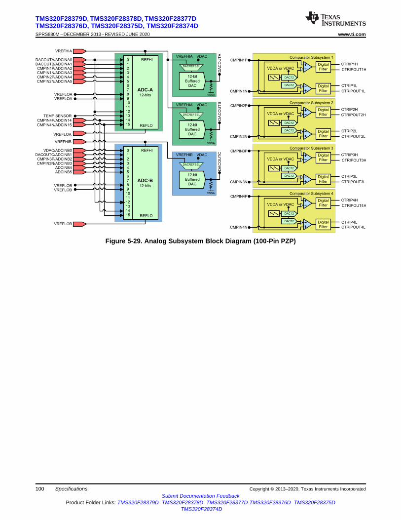
ADC-A
12-bits
0123456789
101112131415
ADC-B
12-bits
DACOUTA/ADCINA0DACOUTB/ADCINA1CMPIN1P/ADCINA2CMPIN1N/ADCINA3
CMPIN4N/ADCIN15
TEMP SENSOR
VDAC/ADCINB0DACOUTC/ADCINB1CMPIN3P/ADCINB2CMPIN3N/ADCINB3
12-bit
Buffered
DAC
CMPIN2P/ADCINA4CMPIN2N/ADCINA5
ADCINB4ADCINB5
VREFHIA
VREFLOB
REFHIVREFHIA
DA
CO
UT
AD
AC
OU
TB
VREFLOBVREFLOB
VDAC
0123456789
101112131415
VREFLOAVREFLOA
CMPIN4P/ADCIN14
CMPIN1P
CMPIN3P
CMPIN2P
CMPIN4P
Comparator Subsystem 1
VDDA or VDAC
CMPIN1N
CTRIPOUT1H
Digital
Filter
CTRIP1H
CTRIP1L
CMPIN2N
CTRIP2L
CTRIP2H
CMPIN3N
CTRIPOUT3H
CTRIP3H
CTRIP3L
CMPIN4N
CTRIPOUT4H
CTRIP4H
CTRIP4L
Digital
Filter CTRIPOUT1L
CTRIPOUT2H
CTRIPOUT2L
CTRIPOUT3L
CTRIPOUT4L
12-bit
Buffered
DAC
VREFHIA VDAC
12-bit
Buffered
DAC
VREFHIB
DA
CO
UT
CVDACREFHI
DAC12
DAC12
Comparator Subsystem 2
VDDA or VDACDigital
Filter
Digital
Filter
DAC12
DAC12
Comparator Subsystem 3
VDDA or VDACDigital
Filter
Digital
Filter
DAC12
DAC12
Comparator Subsystem 4
VDDA or VDACDigital
Filter
Digital
Filter
DAC12
DAC12
REFLO
VREFLOA
VREFHIB
REFLO
VSSA
DACREFSEL
DACREFSEL
DACREFSEL
VSSA
VSSA
100
TMS320F28379D, TMS320F28378D, TMS320F28377DTMS320F28376D, TMS320F28375D, TMS320F28374DSPRS880M –DECEMBER 2013–REVISED JUNE 2020 www.ti.com
Submit Documentation FeedbackProduct Folder Links: TMS320F28379D TMS320F28378D TMS320F28377D TMS320F28376D TMS320F28375D
TMS320F28374D
Specifications Copyright © 2013–2020, Texas Instruments Incorporated
Figure 5-29. Analog Subsystem Block Diagram (100-Pin PZP)
101
TMS320F28379D, TMS320F28378D, TMS320F28377DTMS320F28376D, TMS320F28375D, TMS320F28374D
www.ti.com SPRS880M –DECEMBER 2013–REVISED JUNE 2020
Submit Documentation FeedbackProduct Folder Links: TMS320F28379D TMS320F28378D TMS320F28377D TMS320F28376D TMS320F28375D
TMS320F28374D
SpecificationsCopyright © 2013–2020, Texas Instruments Incorporated
5.10.1 Analog-to-Digital Converter (ADC)The ADCs on this device are successive approximation (SAR) style ADCs with selectable resolution ofeither 16 bits or 12 bits. There are multiple ADC modules which allow simultaneous sampling. The ADCwrapper is start-of-conversion (SOC) based [see the SOC Principle of Operation section of theTMS320F2837xD Dual-Core Microcontrollers Technical Reference Manual.
Each ADC has the following features:• Selectable resolution of 16 bits or 12 bits• Ratiometric external reference set by VREFHI and VREFLO
• Differential signal conversions (16-bit mode only)• Single-ended signal conversions (12-bit mode only)• Input multiplexer with up to 16 channels (single-ended) or 8 channels (differential)• 16 configurable SOCs• 16 individually addressable result registers• Multiple trigger sources
– Software immediate start– All ePWMs– GPIO XINT2– CPU timers– ADCINT1 or 2
• Four flexible PIE interrupts• Burst mode• Four post-processing blocks, each with:
– Saturating offset calibration– Error from setpoint calculation– High, low, and zero-crossing compare, with interrupt and ePWM trip capability– Trigger-to-sample delay capture

Analog to Digital Wrapper LogicAnalog to Digital Core
Input Circuit
Reference Voltage Levels
SOC
Arbitration
& Control
SOCx (0-15)
ADCIN0
Converter
ADCIN1ADCIN2ADCIN3ADCIN4ADCIN5ADCIN6ADCIN7
Interrupt Block (1-4)
Tri
gg
ers
ADCIN8ADCIN9
ADCIN10ADCIN11
0
1
2
3
4
5
6
7
8
9
10
11
VREFLO
VREFHI
CHSEL
ADCSOC
[15:0]
ADCINT1-4
14
15
12
13
ADCIN12ADCIN13ADCIN14ADCIN15
TR
IGS
EL
ACQPS
CHSEL
RESOLUTION
SIGNALMODE
Post Processing Block (1-4)
[15:0]
SIGNALMODE
RESOLUTION
RESULT
AD
CR
ES
UL
T
0–
15
Re
gs
ADCPPBxRESULT
Event
Logic ADCEVTINT
[15:0]
......
ADCEVT
TRIGGER[15:0]
Trigger
Timestamp
SOC Delay
Timestamp
ADCCOUNTER
ADCPPBxOFFCAL
ADCPPBxOFFREF
S+ -
saturate
S
+ -
SO
Cx
ST
AR
T[1
5:0
]
EO
Cx
[15
:0]
CONFIG
u1
x2
x1
S/H Circuit
VIN+
VIN-
DOUT
102
TMS320F28379D, TMS320F28378D, TMS320F28377DTMS320F28376D, TMS320F28375D, TMS320F28374DSPRS880M –DECEMBER 2013–REVISED JUNE 2020 www.ti.com
Submit Documentation FeedbackProduct Folder Links: TMS320F28379D TMS320F28378D TMS320F28377D TMS320F28376D TMS320F28375D
TMS320F28374D
Specifications Copyright © 2013–2020, Texas Instruments Incorporated
Figure 5-30 shows the ADC module block diagram.
Figure 5-30. ADC Module Block Diagram
5.10.1.1 ADC Configurability
Some ADC configurations are individually controlled by the SOCs, while others are controlled by eachADC module. Table 5-41 summarizes the basic ADC options and their level of configurability.
(1) Writing these values differently to different ADC modules could cause the ADCs to operateasynchronously. For guidance on when the ADCs are operating synchronously or asynchronously, seethe Ensuring Synchronous Operation section of the Analog-to-Digital Converter (ADC) chapter in theTMS320F2837xD Dual-Core Microcontrollers Technical Reference Manual.
Table 5-41. ADC Options and Configuration Levels
OPTIONS CONFIGURABILITYClock By the module (1)
Resolution By the module (1)
Signal mode By the moduleReference voltage source Not configurable (external reference only)Trigger source By the SOC (1)
Converted channel By the SOCAcquisition window duration By the SOC (1)
EOC location By the moduleBurst mode By the module (1)

VREFHI
VREFLO
(VSSA)
VREFHI/2
Pin Voltages
ADCINxP
ADCINxN
ADC
ADCINxN
ADCINxP
VREFLO
VREFHI
VREFHI
VREFLO
(VSSA)
Input Common Mode
VREFHI/2 ± 50mVVin Common Mode
+VREFHI
-VREFHI
0
Effective Input Voltage
ADC Vin
2n - 1
0
Digital Output
ADC Vin
103
TMS320F28379D, TMS320F28378D, TMS320F28377DTMS320F28376D, TMS320F28375D, TMS320F28374D
www.ti.com SPRS880M –DECEMBER 2013–REVISED JUNE 2020
Submit Documentation FeedbackProduct Folder Links: TMS320F28379D TMS320F28378D TMS320F28377D TMS320F28376D TMS320F28375D
TMS320F28374D
SpecificationsCopyright © 2013–2020, Texas Instruments Incorporated
5.10.1.1.1 Signal Mode
The ADC supports two signal modes: single-ended and differential. In single-ended mode, the inputvoltage to the converter is sampled through a single pin (ADCINx), referenced to VREFLO. In differentialsignaling mode, the input voltage to the converter is sampled through a pair of input pins, one of which isthe positive input (ADCINxP) and the other is the negative input (ADCINxN). The actual input voltage isthe difference between the two (ADCINxP – ADCINxN). Figure 5-31 shows the differential signaling mode.Figure 5-32 shows the single-ended signaling mode.
Figure 5-31. Differential Signaling Mode

VREFHI
VREFLO
(VSSA)
VREFHI/2
Pin Voltage
ADCINx
ADC
ADCINx
VREFLO
VREFHI
2n - 1
0
Digital Output
ADC Vin
104
TMS320F28379D, TMS320F28378D, TMS320F28377DTMS320F28376D, TMS320F28375D, TMS320F28374DSPRS880M –DECEMBER 2013–REVISED JUNE 2020 www.ti.com
Submit Documentation FeedbackProduct Folder Links: TMS320F28379D TMS320F28378D TMS320F28377D TMS320F28376D TMS320F28375D
TMS320F28374D
Specifications Copyright © 2013–2020, Texas Instruments Incorporated
Figure 5-32. Single-ended Signaling Mode

105
TMS320F28379D, TMS320F28378D, TMS320F28377DTMS320F28376D, TMS320F28375D, TMS320F28374D
www.ti.com SPRS880M –DECEMBER 2013–REVISED JUNE 2020
Submit Documentation FeedbackProduct Folder Links: TMS320F28379D TMS320F28378D TMS320F28377D TMS320F28376D TMS320F28375D
TMS320F28374D
SpecificationsCopyright © 2013–2020, Texas Instruments Incorporated
5.10.1.2 ADC Electrical Data and Timing
Table 5-42 shows the ADC operating conditions for 16-bit differential mode. Table 5-43 shows the ADCcharacteristics for 16-bit differential mode. Table 5-44 shows the ADC operating conditions for 12-bitsingle-ended mode. Table 5-45 shows the ADC characteristics for 12-bit single-ended mode. Table 5-46shows the ADCEXTSOC timing requirements.
(1) The sample window must also be at least as long as 1 ADCCLK cycle for correct ADC operation.(2) VREFCM = (VREFHI + VREFLO)/2(3) The VREFCM requirements will not be met if the negative ADC input pin is connected to VSSA or VREFLO.
Table 5-42. ADC Operating Conditions (16-Bit Differential Mode)over recommended operating conditions (unless otherwise noted)
MIN TYP MAX UNITADCCLK (derived from PERx.SYSCLK) 5 50 MHzSample window duration (set by ACQPS and PERx.SYSCLK) (1) 320 nsVREFHI 2.4 2.5 or 3.0 VDDA VVREFLO VSSA 0 VSSA VVREFHI – VREFLO 2.4 VDDA VADC input conversion range VREFLO VREFHI VADC input signal common mode voltage (2) (3) VREFCM – 50 VREFCM VREFCM + 50 mV
NOTEThe ADC inputs should be kept below VDDA + 0.3 V during operation. If an ADC inputexceeds this level, the VREF internal to the device may be disturbed, which can impact resultsfor other ADC or DAC inputs using the same VREF.
NOTEThe VREFHI pin must be kept below VDDA + 0.3 V to ensure proper functional operation. If theVREFHI pin exceeds this level, a blocking circuit may activate, and the internal value of VREFHImay float to 0 V internally, giving improper ADC conversion or DAC output.

106
TMS320F28379D, TMS320F28378D, TMS320F28377DTMS320F28376D, TMS320F28375D, TMS320F28374DSPRS880M –DECEMBER 2013–REVISED JUNE 2020 www.ti.com
Submit Documentation FeedbackProduct Folder Links: TMS320F28379D TMS320F28378D TMS320F28377D TMS320F28376D TMS320F28375D
TMS320F28374D
Specifications Copyright © 2013–2020, Texas Instruments Incorporated
(1) Typical values are measured with VREFHI = 2.5 V and VREFLO = 0 V. Minimum and Maximum values are tested or characterized withVREFHI = 2.5 V and VREFLO = 0 V.
(2) See Section 5.10.1.2.2.(3) Difference from conversion result 32768 when ADCINp = ADCINn = VREFCM.(4) No missing codes.(5) AC parameters will be impacted by clock source accuracy and jitter, this should be taken into account when selecting the clock source
for the system. The clock source used for these parameters was a high-accuracy external clock fed through the PLL. The on-chipInternal Oscillator has higher jitter than an external crystal and these parameters will degrade if it is used as a clock source.
(6) I/O activity is minimized on pins adjacent to ADC input and VREFHI pins as part of best practices to reduce capacitive coupling andcrosstalk.
(7) One ADC operating while all other ADCs are idle.(8) All ADCs operating with identical ADCCLK, S+H durations, triggers, and resolution.(9) Any ADCs operating with heterogeneous ADCCLK, S+H durations, triggers, or resolution.(10) Maximum DC code deviation due to operation of multiple ADCs simultaneously.(11) Value based on characterization.
Table 5-43. ADC Characteristics (16-Bit Differential Mode)over recommended operating conditions (unless otherwise noted) (1)
PARAMETER TEST CONDITIONS MIN TYP MAX UNITADC conversion cycles (2) 29.6 31 ADCCLKsPower-up time (after settingADCPWDNZ to first conversion) 500 µs
Gain error –64 ±9 64 LSBsOffset error (3) –16 ±9 16 LSBsChannel-to-channel gain error ±6 LSBsChannel-to-channel offset error ±3 LSBsADC-to-ADC gain error Identical VREFHI and VREFLO for all ADCs ±6 LSBsADC-to-ADC offset error Identical VREFHI and VREFLO for all ADCs ±3 LSBsDNL (4) > –1 ±0.5 1 LSBsINL –3 ±1.5 3 LSBsSNR (5) (6) VREFHI = 2.5 V, fin = 10 kHz 87.6 dBTHD (5) (6) VREFHI = 2.5 V, fin = 10 kHz –93.5 dBSFDR (5) (6) VREFHI = 2.5 V, fin = 10 kHz 95.4 dBSINAD (5) (6) VREFHI = 2.5 V, fin = 10 kHz 86.6 dB
ENOB (5) (6)
VREFHI = 2.5 V, fin = 10 kHz,single ADC (7) 14.1
bitsVREFHI = 2.5 V, fin = 10 kHz,synchronous ADCs (8) 14.1
VREFHI = 2.5 V, fin = 10 kHz,asynchronous ADCs (9)
Notsupported
PSRR VDDA = 3.3-V DC + 200 mVDC up to Sine at 1 kHz 77 dB
PSRR VDDA = 3.3-V DC + 200 mVSine at 800 kHz 74 dB
CMRR DC to 1 MHz 60 dBVREFHI input current 190 µA
ADC-to-ADC isolation (6) (10) (11)VREFHI = 2.5 V, synchronous ADCs (8) –2 2
LSBsVREFHI = 2.5 V, asynchronous ADCs (9) Not
supported
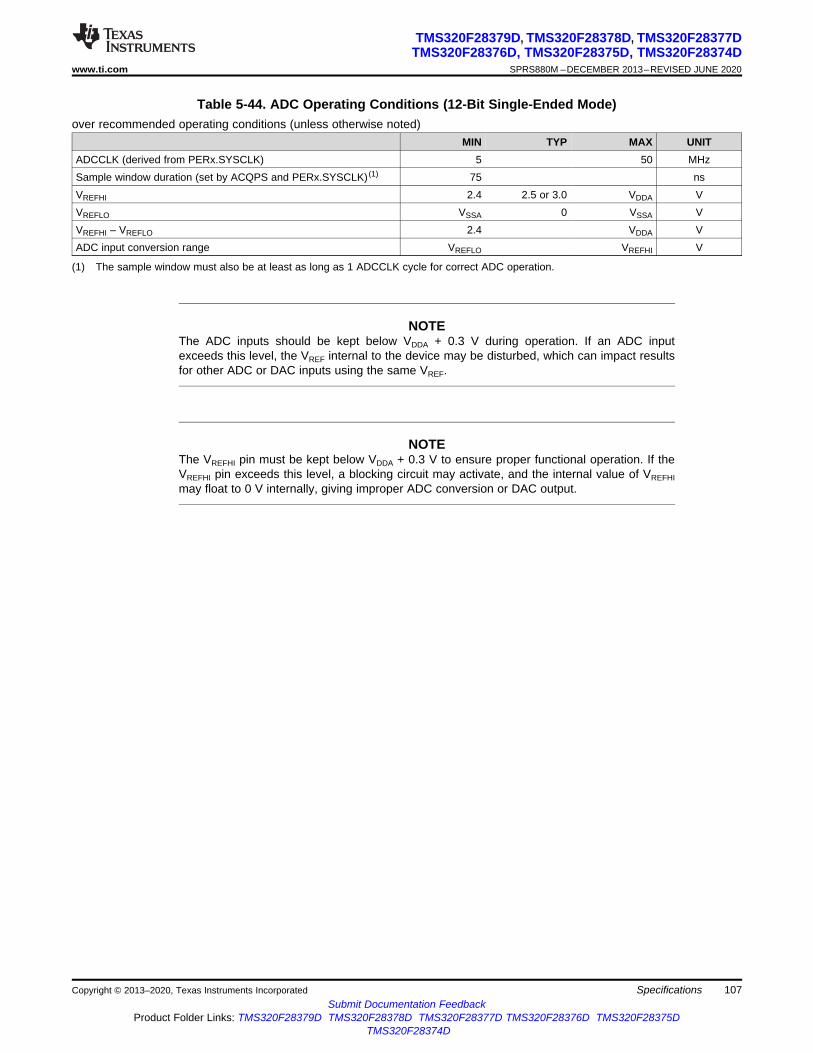
107
TMS320F28379D, TMS320F28378D, TMS320F28377DTMS320F28376D, TMS320F28375D, TMS320F28374D
www.ti.com SPRS880M –DECEMBER 2013–REVISED JUNE 2020
Submit Documentation FeedbackProduct Folder Links: TMS320F28379D TMS320F28378D TMS320F28377D TMS320F28376D TMS320F28375D
TMS320F28374D
SpecificationsCopyright © 2013–2020, Texas Instruments Incorporated
(1) The sample window must also be at least as long as 1 ADCCLK cycle for correct ADC operation.
Table 5-44. ADC Operating Conditions (12-Bit Single-Ended Mode)over recommended operating conditions (unless otherwise noted)
MIN TYP MAX UNITADCCLK (derived from PERx.SYSCLK) 5 50 MHzSample window duration (set by ACQPS and PERx.SYSCLK) (1) 75 nsVREFHI 2.4 2.5 or 3.0 VDDA VVREFLO VSSA 0 VSSA VVREFHI – VREFLO 2.4 VDDA VADC input conversion range VREFLO VREFHI V
NOTEThe ADC inputs should be kept below VDDA + 0.3 V during operation. If an ADC inputexceeds this level, the VREF internal to the device may be disturbed, which can impact resultsfor other ADC or DAC inputs using the same VREF.
NOTEThe VREFHI pin must be kept below VDDA + 0.3 V to ensure proper functional operation. If theVREFHI pin exceeds this level, a blocking circuit may activate, and the internal value of VREFHImay float to 0 V internally, giving improper ADC conversion or DAC output.

108
TMS320F28379D, TMS320F28378D, TMS320F28377DTMS320F28376D, TMS320F28375D, TMS320F28374DSPRS880M –DECEMBER 2013–REVISED JUNE 2020 www.ti.com
Submit Documentation FeedbackProduct Folder Links: TMS320F28379D TMS320F28378D TMS320F28377D TMS320F28376D TMS320F28375D
TMS320F28374D
Specifications Copyright © 2013–2020, Texas Instruments Incorporated
(1) Typical values are measured with VREFHI = 2.5 V and VREFLO = 0 V. Minimum and Maximum values are tested or characterized withVREFHI = 2.5 V and VREFLO = 0 V.
(2) See Section 5.10.1.2.2.(3) No missing codes.(4) AC parameters will be impacted by clock source accuracy and jitter, this should be taken into account when selecting the clock source
for the system. The clock source used for these parameters was a high-accuracy external clock fed through the PLL. The on-chipInternal Oscillator has higher jitter than an external crystal and these parameters will degrade if it is used as a clock source.
(5) I/O activity is minimized on pins adjacent to ADC input and VREFHI pins as part of best practices to reduce capacitive coupling andcrosstalk.
(6) One ADC operating while all other ADCs are idle.(7) All ADCs operating with identical ADCCLK, S+H durations, triggers, and resolution.(8) Any ADCs operating with heterogeneous ADCCLK, S+H durations, triggers, or resolution.(9) Maximum DC code deviation due to operation of multiple ADCs simultaneously.(10) Value based on characterization.
Table 5-45. ADC Characteristics (12-Bit Single-Ended Mode)over recommended operating conditions (unless otherwise noted) (1)
PARAMETER TEST CONDITIONS MIN TYP MAX UNITADC conversion cycles (2) 10.1 11 ADCCLKsPower-up time 500 µsGain error –5 ±3 5 LSBsOffset error –4 ±2 4 LSBsChannel-to-channel gain error ±4 LSBsChannel-to-channel offset error ±2 LSBsADC-to-ADC gain error Identical VREFHI and VREFLO for all ADCs ±4 LSBsADC-to-ADC offset error Identical VREFHI and VREFLO for all ADCs ±2 LSBsDNL (3) > –1 ±0.5 1 LSBsINL –2 ±1.0 2 LSBsSNR (4) (5) VREFHI = 2.5 V, fin = 100 kHz 68.8 dBTHD (4) (5) VREFHI = 2.5 V, fin = 100 kHz –78.4 dBSFDR (4) (5) VREFHI = 2.5 V, fin = 100 kHz 79.2 dBSINAD (4) (5) VREFHI = 2.5 V, fin = 100 kHz 68.4 dB
ENOB (4) (5)
VREFHI = 2.5 V, fin = 100 kHz,single ADC (6), all packages 11.1
bits
VREFHI = 2.5 V, fin = 100 kHz,synchronous ADCs (7), all packages 11.1
VREFHI = 2.5 V, fin = 100 kHz,asynchronous ADCs (8),100-pin PZP package
Notsupported
VREFHI = 2.5 V, fin = 100 kHz,asynchronous ADCs (8),176-pin PTP package
9.7
VREFHI = 2.5 V, fin = 100 kHz,asynchronous ADCs (8),337-ball ZWT package
10.9
PSRR VDDA = 3.3-V DC + 200 mVDC up to Sine at 1 kHz 60 dB
PSRR VDDA = 3.3-V DC + 200 mVSine at 800 kHz 57 dB
ADC-to-ADC isolation (5) (9) (10)
VREFHI = 2.5 V, synchronous ADCs (7),all packages –1 1
LSBs
VREFHI = 2.5 V, asynchronous ADCs (8),100-pin PZP package
Notsupported
VREFHI = 2.5 V, asynchronous ADCs (8),176-pin PTP package –9 9
VREFHI = 2.5 V, asynchronous ADCs (8),337-ball ZWT package –2 2
VREFHI input current 130 µA
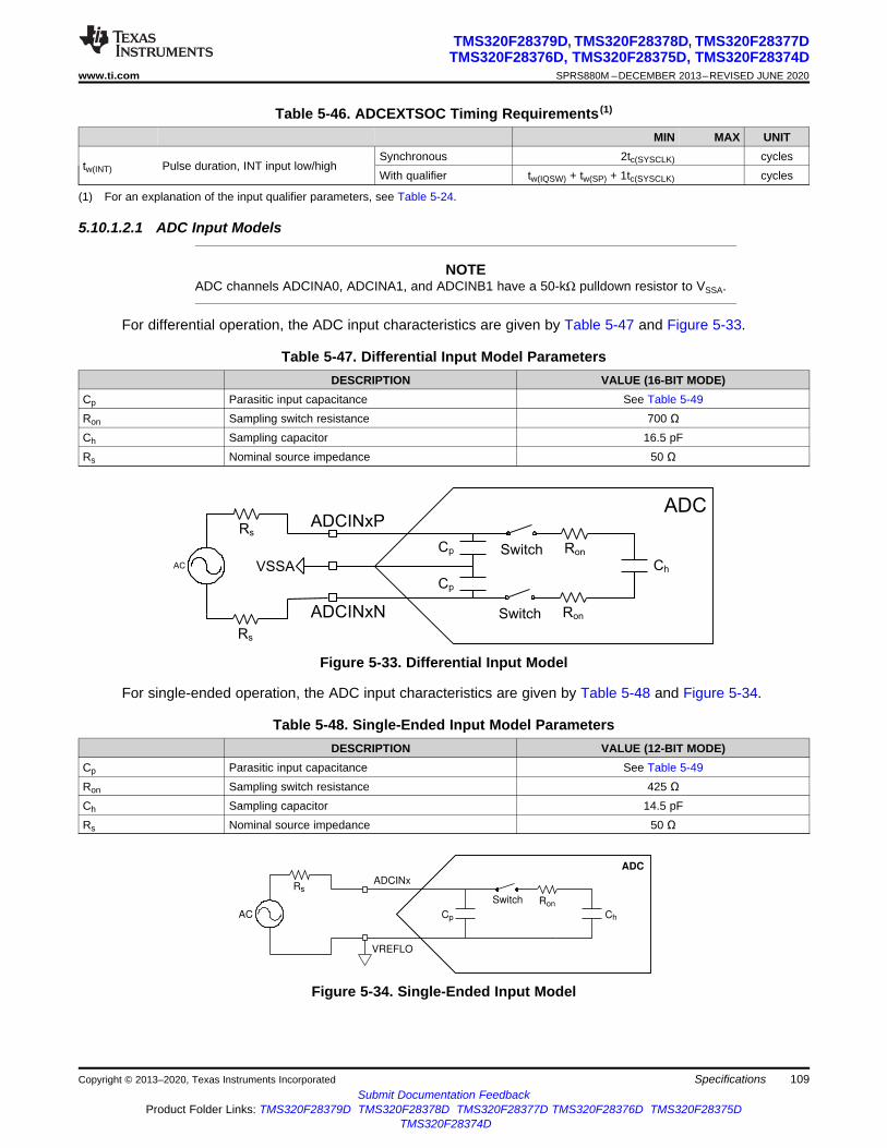
ADC
RonSwitch
VREFLO
ChCp
ADCINx
AC
Rs
ADC
RonSwitch
ADCINxN
Ch
Cp
ADCINxP
AC
Rs
RonSwitch
Rs
Cp
VSSA
109
TMS320F28379D, TMS320F28378D, TMS320F28377DTMS320F28376D, TMS320F28375D, TMS320F28374D
www.ti.com SPRS880M –DECEMBER 2013–REVISED JUNE 2020
Submit Documentation FeedbackProduct Folder Links: TMS320F28379D TMS320F28378D TMS320F28377D TMS320F28376D TMS320F28375D
TMS320F28374D
SpecificationsCopyright © 2013–2020, Texas Instruments Incorporated
(1) For an explanation of the input qualifier parameters, see Table 5-24.
Table 5-46. ADCEXTSOC Timing Requirements (1)
MIN MAX UNIT
tw(INT) Pulse duration, INT input low/highSynchronous 2tc(SYSCLK) cyclesWith qualifier tw(IQSW) + tw(SP) + 1tc(SYSCLK) cycles
5.10.1.2.1 ADC Input Models
NOTEADC channels ADCINA0, ADCINA1, and ADCINB1 have a 50-kΩ pulldown resistor to VSSA.
For differential operation, the ADC input characteristics are given by Table 5-47 and Figure 5-33.
Table 5-47. Differential Input Model ParametersDESCRIPTION VALUE (16-BIT MODE)
Cp Parasitic input capacitance See Table 5-49Ron Sampling switch resistance 700 ΩCh Sampling capacitor 16.5 pFRs Nominal source impedance 50 Ω
Figure 5-33. Differential Input Model
For single-ended operation, the ADC input characteristics are given by Table 5-48 and Figure 5-34.
Table 5-48. Single-Ended Input Model ParametersDESCRIPTION VALUE (12-BIT MODE)
Cp Parasitic input capacitance See Table 5-49Ron Sampling switch resistance 425 ΩCh Sampling capacitor 14.5 pFRs Nominal source impedance 50 Ω
Figure 5-34. Single-Ended Input Model

110
TMS320F28379D, TMS320F28378D, TMS320F28377DTMS320F28376D, TMS320F28375D, TMS320F28374DSPRS880M –DECEMBER 2013–REVISED JUNE 2020 www.ti.com
Submit Documentation FeedbackProduct Folder Links: TMS320F28379D TMS320F28378D TMS320F28377D TMS320F28376D TMS320F28375D
TMS320F28374D
Specifications Copyright © 2013–2020, Texas Instruments Incorporated
Table 5-49 shows the parasitic capacitance on each channel. Also, enabling a comparator addsapproximately 1.4 pF of capacitance on positive comparator inputs and 2.5 pF of capacitance on negativecomparator inputs.
(1) The increased capacitance is due to VDAC functionality.
Table 5-49. Per-Channel Parasitic Capacitance
ADC CHANNELCp (pF)
COMPARATOR DISABLED COMPARATOR ENABLEDADCINA0 12.9 N/AADCINA1 10.3 N/AADCINA2 5.9 7.3ADCINA3 6.3 8.8ADCINA4 5.9 7.3ADCINA5 6.3 8.8
ADCINB0 (1) 117.0 N/AADCINB1 10.6 N/AADCINB2 5.9 7.3ADCINB3 6.2 8.7ADCINB4 5.2 N/AADCINB5 5.1 N/AADCINC2 5.5 6.9ADCINC3 5.8 8.3ADCINC4 5.0 6.4ADCINC5 5.3 7.8ADCIND0 5.3 6.7ADCIND1 5.7 8.2ADCIND2 5.3 6.7ADCIND3 5.6 8.1ADCIND4 4.3 N/AADCIND5 4.3 N/AADCIN14 8.6 10.0ADCIN15 9.0 11.5
These input models should be used along with actual signal source impedance to determine theacquisition window duration. See the Choosing an Acquisition Window Duration section of theTMS320F2837xD Dual-Core Microcontrollers Technical Reference Manual for more information.
The user should analyze the ADC input setting assuming worst-case initial conditions on Ch. This willrequire assuming that Ch could start the S+H window completely charged to VREFHI or completelydischarged to VREFLO. When the ADC transitions from an odd-numbered channel to an even-numberedchannel, or vice-versa, the actual initial voltage on Ch will be close to being completely discharged toVREFLO. For even-to-even or odd-to-odd channel transitions, the initial voltage on Ch will be close to thevoltage of the previously converted channel.
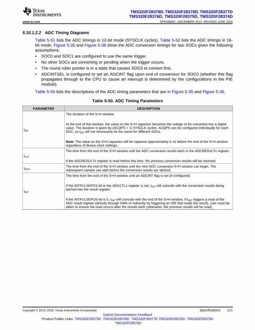
111
TMS320F28379D, TMS320F28378D, TMS320F28377DTMS320F28376D, TMS320F28375D, TMS320F28374D
www.ti.com SPRS880M –DECEMBER 2013–REVISED JUNE 2020
Submit Documentation FeedbackProduct Folder Links: TMS320F28379D TMS320F28378D TMS320F28377D TMS320F28376D TMS320F28375D
TMS320F28374D
SpecificationsCopyright © 2013–2020, Texas Instruments Incorporated
5.10.1.2.2 ADC Timing Diagrams
Table 5-51 lists the ADC timings in 12-bit mode (SYSCLK cycles). Table 5-52 lists the ADC timings in 16-bit mode. Figure 5-35 and Figure 5-36 show the ADC conversion timings for two SOCs given the followingassumptions:• SOC0 and SOC1 are configured to use the same trigger.• No other SOCs are converting or pending when the trigger occurs.• The round robin pointer is in a state that causes SOC0 to convert first.• ADCINTSEL is configured to set an ADCINT flag upon end of conversion for SOC0 (whether this flag
propagates through to the CPU to cause an interrupt is determined by the configurations in the PIEmodule).
Table 5-50 lists the descriptions of the ADC timing parameters that are in Figure 5-35 and Figure 5-36.
Table 5-50. ADC Timing Parameters
PARAMETER DESCRIPTION
tSH
The duration of the S+H window.
At the end of this window, the value on the S+H capacitor becomes the voltage to be converted into a digitalvalue. The duration is given by (ACQPS + 1) SYSCLK cycles. ACQPS can be configured individually for eachSOC, so tSH will not necessarily be the same for different SOCs.
Note: The value on the S+H capacitor will be captured approximately 5 ns before the end of the S+H windowregardless of device clock settings.
tLAT
The time from the end of the S+H window until the ADC conversion results latch in the ADCRESULTx register.
If the ADCRESULTx register is read before this time, the previous conversion results will be returned.
tEOCThe time from the end of the S+H window until the next ADC conversion S+H window can begin. Thesubsequent sample can start before the conversion results are latched.
tINT
The time from the end of the S+H window until an ADCINT flag is set (if configured).
If the INTPULSEPOS bit in the ADCCTL1 register is set, tINT will coincide with the conversion results beinglatched into the result register.
If the INTPULSEPOS bit is 0, tINT will coincide with the end of the S+H window. If tINT triggers a read of theADC result register (directly through DMA or indirectly by triggering an ISR that reads the result), care must betaken to ensure the read occurs after the results latch (otherwise, the previous results will be read).
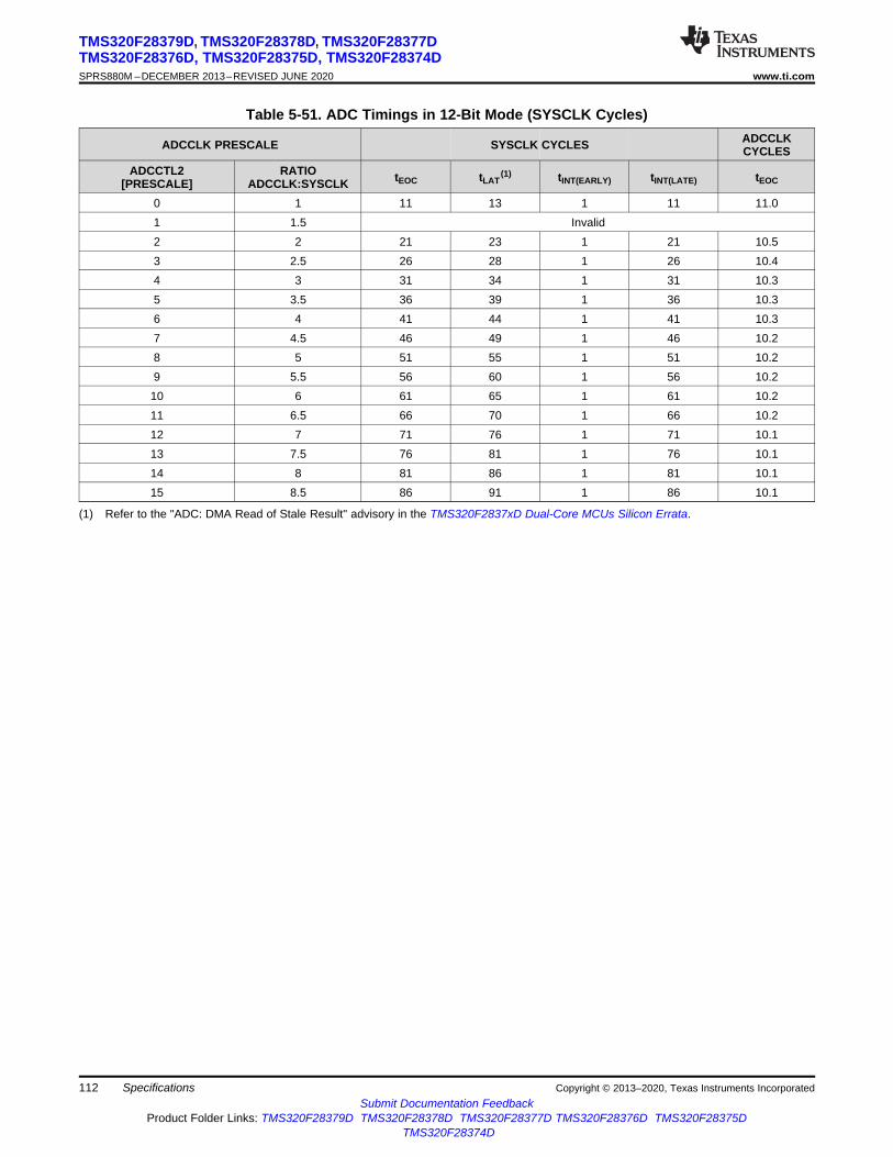
112
TMS320F28379D, TMS320F28378D, TMS320F28377DTMS320F28376D, TMS320F28375D, TMS320F28374DSPRS880M –DECEMBER 2013–REVISED JUNE 2020 www.ti.com
Submit Documentation FeedbackProduct Folder Links: TMS320F28379D TMS320F28378D TMS320F28377D TMS320F28376D TMS320F28375D
TMS320F28374D
Specifications Copyright © 2013–2020, Texas Instruments Incorporated
(1) Refer to the "ADC: DMA Read of Stale Result" advisory in the TMS320F2837xD Dual-Core MCUs Silicon Errata.
Table 5-51. ADC Timings in 12-Bit Mode (SYSCLK Cycles)
ADCCLK PRESCALE SYSCLK CYCLES ADCCLKCYCLES
ADCCTL2[PRESCALE]
RATIOADCCLK:SYSCLK tEOC tLAT
(1) tINT(EARLY) tINT(LATE) tEOC
0 1 11 13 1 11 11.01 1.5 Invalid2 2 21 23 1 21 10.53 2.5 26 28 1 26 10.44 3 31 34 1 31 10.35 3.5 36 39 1 36 10.36 4 41 44 1 41 10.37 4.5 46 49 1 46 10.28 5 51 55 1 51 10.29 5.5 56 60 1 56 10.210 6 61 65 1 61 10.211 6.5 66 70 1 66 10.212 7 71 76 1 71 10.113 7.5 76 81 1 76 10.114 8 81 86 1 81 10.115 8.5 86 91 1 86 10.1
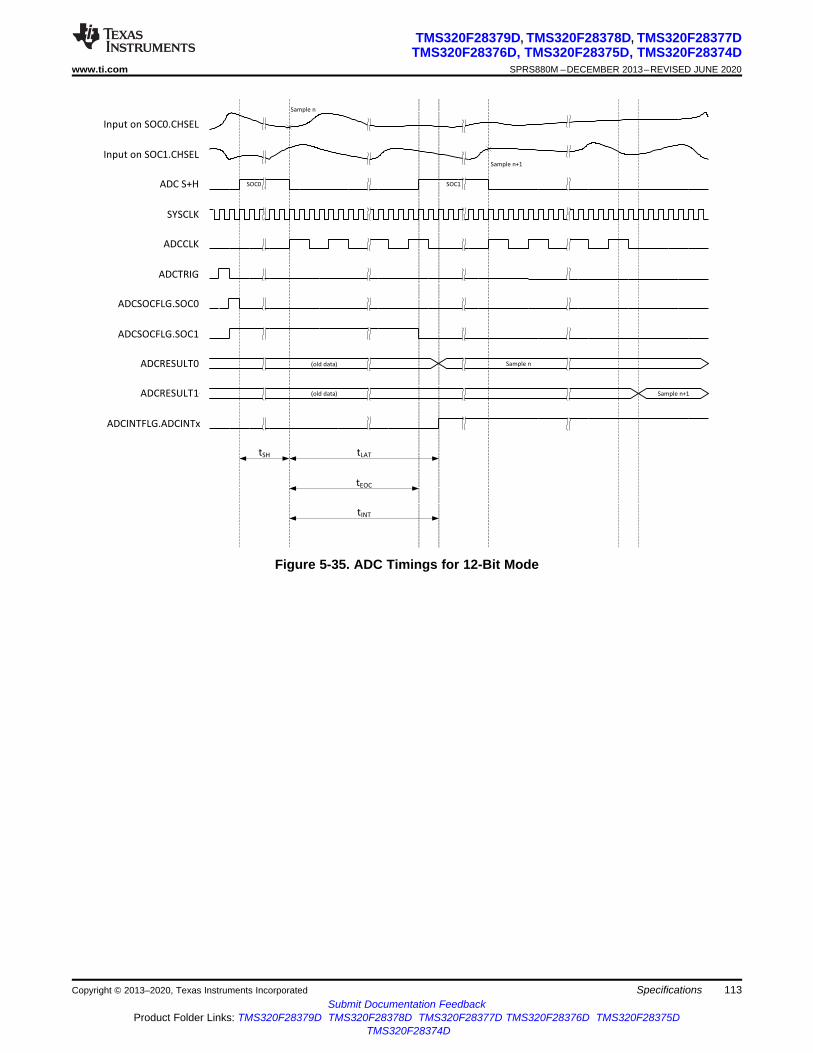
SYSCLK
ADCTRIG
ADCSOCFLG.SOC0
ADCSOCFLG.SOC1
ADC S+H
ADCCLK
SOC0
Input on SOC0.CHSEL
Input on SOC1.CHSEL
ADCRESULT0
ADCRESULT1
ADCINTFLG.ADCINTx
SOC1
(old data)
(old data)
Sample n
Sample n+1
Sample n
Sample n+1
tSH tLAT
tEOC
tINT
113
TMS320F28379D, TMS320F28378D, TMS320F28377DTMS320F28376D, TMS320F28375D, TMS320F28374D
www.ti.com SPRS880M –DECEMBER 2013–REVISED JUNE 2020
Submit Documentation FeedbackProduct Folder Links: TMS320F28379D TMS320F28378D TMS320F28377D TMS320F28376D TMS320F28375D
TMS320F28374D
SpecificationsCopyright © 2013–2020, Texas Instruments Incorporated
Figure 5-35. ADC Timings for 12-Bit Mode

114
TMS320F28379D, TMS320F28378D, TMS320F28377DTMS320F28376D, TMS320F28375D, TMS320F28374DSPRS880M –DECEMBER 2013–REVISED JUNE 2020 www.ti.com
Submit Documentation FeedbackProduct Folder Links: TMS320F28379D TMS320F28378D TMS320F28377D TMS320F28376D TMS320F28375D
TMS320F28374D
Specifications Copyright © 2013–2020, Texas Instruments Incorporated
(1) Refer to the "ADC: DMA Read of Stale Result" advisory in the TMS320F2837xD Dual-Core MCUs Silicon Errata.
Table 5-52. ADC Timings in 16-Bit Mode
ADCCLK PRESCALE SYSCLK CYCLES ADCCLKCYCLES
ADCCTL2[PRESCALE]
RATIOADCCLK:SYSCLK tEOC tLAT
(1) tINT(EARLY) tINT(LATE) tEOC
0 1 31 32 1 31 31.01 1.5 Invalid2 2 60 61 1 60 30.03 2.5 75 75 1 75 30.04 3 90 91 1 90 30.05 3.5 104 106 1 104 29.76 4 119 120 1 119 29.87 4.5 134 134 1 134 29.88 5 149 150 1 149 29.89 5.5 163 165 1 163 29.610 6 178 179 1 178 29.711 6.5 193 193 1 193 29.712 7 208 209 1 208 29.713 7.5 222 224 1 222 29.614 8 237 238 1 237 29.615 8.5 252 252 1 252 29.6

SYSCLK
ADCTRIG
ADCSOCFLG.SOC0
ADCSOCFLG.SOC1
ADC S+H
ADCCLK
SOC0
Input on SOC0.CHSEL
Input on SOC1.CHSEL
ADCRESULT0
ADCRESULT1
ADCINTFLG.ADCINTx
SOC1
(old data)
(old data)
Sample n
Sample n+1
Sample n
Sample n+1
tSH tLAT
tEOC
tINT
115
TMS320F28379D, TMS320F28378D, TMS320F28377DTMS320F28376D, TMS320F28375D, TMS320F28374D
www.ti.com SPRS880M –DECEMBER 2013–REVISED JUNE 2020
Submit Documentation FeedbackProduct Folder Links: TMS320F28379D TMS320F28378D TMS320F28377D TMS320F28376D TMS320F28375D
TMS320F28374D
SpecificationsCopyright © 2013–2020, Texas Instruments Incorporated
Figure 5-36. ADC Timings for 16-Bit Mode

116
TMS320F28379D, TMS320F28378D, TMS320F28377DTMS320F28376D, TMS320F28375D, TMS320F28374DSPRS880M –DECEMBER 2013–REVISED JUNE 2020 www.ti.com
Submit Documentation FeedbackProduct Folder Links: TMS320F28379D TMS320F28378D TMS320F28377D TMS320F28376D TMS320F28375D
TMS320F28374D
Specifications Copyright © 2013–2020, Texas Instruments Incorporated
5.10.1.3 Temperature Sensor Electrical Data and Timing
The temperature sensor can be used to measure the device junction temperature. The temperaturesensor is sampled through an internal connection to the ADC and translated into a temperature throughTI-provided software. When sampling the temperature sensor, the ADC must meet the acquisition time inTable 5-53.
Table 5-53. Temperature Sensor Electrical Characteristicsover recommended operating conditions (unless otherwise noted)
PARAMETER MIN TYP MAX UNITTemperature accuracy ±15 °CStart-up time (TSNSCTL[ENABLE] to sampling temperature sensor) 500 µsADC acquisition time 700 ns

CTRIPOUT1H
CTRIP1H
CTRIP1L
CTRIP2L
CTRIPOUT2H
CTRIP2H
CTRIPOUT8H
CTRIP8H
CTRIP8L
ePWMsePWM X-BAR
CTRIPOUT2L
CTRIPOUT8L
CTRIP1HCTRIP1LCTRIP2HCTRIP2L
CTRIP8HCTRIP8L
GPIO MuxOutput X-BAR
CTRIPOUT1HCTRIPOUT1LCTRIPOUT2HCTRIPOUT2L
CTRIPOUT8HCTRIPOUT8L
Comparator Subsystem 1
VDDA or VDACDigital
Filter
Digital
Filter
DAC12
DAC12
CTRIPOUT1L
Comparator Subsystem 2
VDDA or VDACDigital
Filter
Digital
Filter
DAC12
DAC12
Comparator Subsystem 8
VDDA or VDACDigital
Filter
Digital
Filter
DAC12
DAC12
CMPIN1P Pin
CMPIN1N Pin
CMPIN2N Pin
CMPIN8N Pin
CMPIN2P Pin
CMPIN8P Pin
117
TMS320F28379D, TMS320F28378D, TMS320F28377DTMS320F28376D, TMS320F28375D, TMS320F28374D
www.ti.com SPRS880M –DECEMBER 2013–REVISED JUNE 2020
Submit Documentation FeedbackProduct Folder Links: TMS320F28379D TMS320F28378D TMS320F28377D TMS320F28376D TMS320F28375D
TMS320F28374D
SpecificationsCopyright © 2013–2020, Texas Instruments Incorporated
5.10.2 Comparator Subsystem (CMPSS)Each CMPSS module includes two comparators, two internal voltage reference DACs (CMPSS DACs),two digital glitch filters, and one ramp generator. There are two inputs, CMPINxP and CMPINxN. Each ofthese inputs will be internally connected to an ADCIN pin. The CMPINxP pin is always connected to thepositive input of the CMPSS comparators. CMPINxN can be used instead of the DAC output to drive thenegative comparator inputs. There are two comparators, and therefore two outputs from the CMPSSmodule, which are connected to the input of a digital filter module before being passed on to theComparator TRIP crossbar and either PWM modules or directly to a GPIO pin. Figure 5-37 shows theCMPSS connectivity on the 337-ball ZWT and 176-pin PTP packages. Figure 5-38 shows CMPSSconnectivity on the 100-pin PZP package.
Figure 5-37. CMPSS Connectivity (337-Ball ZWT and 176-Pin PTP)
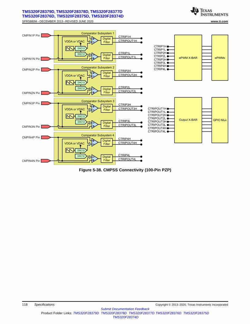
CTRIPOUT1H
CTRIP1H
CTRIP1L
CTRIP2L
CTRIPOUT2H
CTRIP2H
CTRIPOUT4H
CTRIP4H
CTRIP4L
ePWMsePWM X-BAR
CTRIPOUT2L
CTRIPOUT4L
GPIO MuxOutput X-BAR
Comparator Subsystem 1
VDDA or VDACDigital
Filter
Digital
Filter
DAC12
DAC12
CTRIPOUT1L
Comparator Subsystem 2
VDDA or VDACDigital
Filter
Digital
Filter
DAC12
DAC12
Comparator Subsystem 4
VDDA or VDACDigital
Filter
Digital
Filter
DAC12
DAC12
CTRIPOUT3H
CTRIP3H
CTRIP3L
CTRIPOUT3L
Comparator Subsystem 3
VDDA or VDACDigital
Filter
Digital
Filter
DAC12
DAC12
CTRIP1HCTRIP1LCTRIP2HCTRIP2L
CTRIP4HCTRIP4L
CTRIP3HCTRIP3L
CTRIPOUT1HCTRIPOUT1LCTRIPOUT2HCTRIPOUT2L
CTRIPOUT4HCTRIPOUT4L
CTRIPOUT3HCTRIPOUT3L
CMPIN1P Pin
CMPIN2P Pin
CMPIN3P Pin
CMPIN4P Pin
CMPIN1N Pin
CMPIN2N Pin
CMPIN3N Pin
CMPIN4N Pin
118
TMS320F28379D, TMS320F28378D, TMS320F28377DTMS320F28376D, TMS320F28375D, TMS320F28374DSPRS880M –DECEMBER 2013–REVISED JUNE 2020 www.ti.com
Submit Documentation FeedbackProduct Folder Links: TMS320F28379D TMS320F28378D TMS320F28377D TMS320F28376D TMS320F28375D
TMS320F28374D
Specifications Copyright © 2013–2020, Texas Instruments Incorporated
Figure 5-38. CMPSS Connectivity (100-Pin PZP)
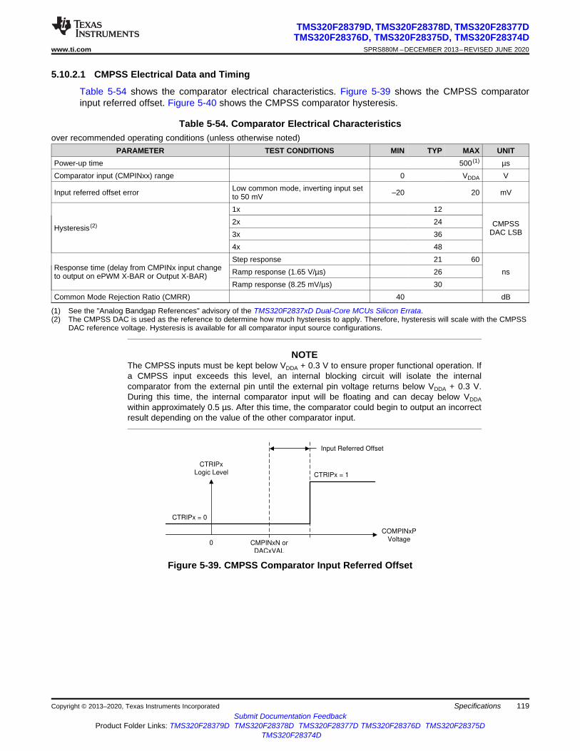
CTRIPx = 0
0 CMPINxN or
DACxVAL
CTRIPx = 1
Input Referred Offset
COMPINxP
Voltage
CTRIPx
Logic Level
119
TMS320F28379D, TMS320F28378D, TMS320F28377DTMS320F28376D, TMS320F28375D, TMS320F28374D
www.ti.com SPRS880M –DECEMBER 2013–REVISED JUNE 2020
Submit Documentation FeedbackProduct Folder Links: TMS320F28379D TMS320F28378D TMS320F28377D TMS320F28376D TMS320F28375D
TMS320F28374D
SpecificationsCopyright © 2013–2020, Texas Instruments Incorporated
5.10.2.1 CMPSS Electrical Data and Timing
Table 5-54 shows the comparator electrical characteristics. Figure 5-39 shows the CMPSS comparatorinput referred offset. Figure 5-40 shows the CMPSS comparator hysteresis.
(1) See the "Analog Bandgap References" advisory of the TMS320F2837xD Dual-Core MCUs Silicon Errata.(2) The CMPSS DAC is used as the reference to determine how much hysteresis to apply. Therefore, hysteresis will scale with the CMPSS
DAC reference voltage. Hysteresis is available for all comparator input source configurations.
Table 5-54. Comparator Electrical Characteristicsover recommended operating conditions (unless otherwise noted)
PARAMETER TEST CONDITIONS MIN TYP MAX UNITPower-up time 500 (1) µsComparator input (CMPINxx) range 0 VDDA V
Input referred offset error Low common mode, inverting input setto 50 mV –20 20 mV
Hysteresis (2)
1x 12
CMPSSDAC LSB
2x 243x 364x 48
Response time (delay from CMPINx input changeto output on ePWM X-BAR or Output X-BAR)
Step response 21 60nsRamp response (1.65 V/µs) 26
Ramp response (8.25 mV/µs) 30Common Mode Rejection Ratio (CMRR) 40 dB
NOTEThe CMPSS inputs must be kept below VDDA + 0.3 V to ensure proper functional operation. Ifa CMPSS input exceeds this level, an internal blocking circuit will isolate the internalcomparator from the external pin until the external pin voltage returns below VDDA + 0.3 V.During this time, the internal comparator input will be floating and can decay below VDDAwithin approximately 0.5 µs. After this time, the comparator could begin to output an incorrectresult depending on the value of the other comparator input.
Figure 5-39. CMPSS Comparator Input Referred Offset

CTRIPx = 0
0 CMPINxN or
DACxVAL
CTRIPx = 1
Hysteresis
COMPINxP
Voltage
CTRIPx
Logic Level
120
TMS320F28379D, TMS320F28378D, TMS320F28377DTMS320F28376D, TMS320F28375D, TMS320F28374DSPRS880M –DECEMBER 2013–REVISED JUNE 2020 www.ti.com
Submit Documentation FeedbackProduct Folder Links: TMS320F28379D TMS320F28378D TMS320F28377D TMS320F28376D TMS320F28375D
TMS320F28374D
Specifications Copyright © 2013–2020, Texas Instruments Incorporated
Figure 5-40. CMPSS Comparator Hysteresis

Offset Error
121
TMS320F28379D, TMS320F28378D, TMS320F28377DTMS320F28376D, TMS320F28375D, TMS320F28374D
www.ti.com SPRS880M –DECEMBER 2013–REVISED JUNE 2020
Submit Documentation FeedbackProduct Folder Links: TMS320F28379D TMS320F28378D TMS320F28377D TMS320F28376D TMS320F28375D
TMS320F28374D
SpecificationsCopyright © 2013–2020, Texas Instruments Incorporated
Table 5-55 shows the CMPSS DAC static electrical characteristics. Figure 5-41 shows the CMPSS DACstatic offset. Figure 5-42 shows the CMPSS DAC static gain. Figure 5-43 shows the CMPSS DAC staticlinearity.
(1) The maximum output voltage is VDDA when VDAC > VDDA.(2) Includes comparator input referred errors.(3) Disturbance error may be present on the CMPSS DAC output for a certain amount of time after a comparator trip.(4) Per active CMPSS module.
Table 5-55. CMPSS DAC Static Electrical Characteristicsover recommended operating conditions (unless otherwise noted)
PARAMETER TEST CONDITIONS MIN TYP MAX UNIT
CMPSS DAC output rangeInternal reference 0 VDDA
(1)V
External reference 0 VDACStatic offset error (2) –25 25 mVStatic gain error (2) –2 2 % of FSRStatic DNL Endpoint corrected >–1 4 LSBStatic INL Endpoint corrected –16 16 LSB
Settling time Settling to 1 LSB after full-scale outputchange 1 µs
Resolution 12 bits
CMPSS DAC output disturbance (3)Error induced by comparator trip orCMPSS DAC code change within thesame CMPSS module
–100 100 LSB
CMPSS DAC disturbance time (3) 200 nsVDAC reference voltage When VDAC is reference 2.4 2.5 or 3.0 VDDA VVDAC load (4) When VDAC is reference 6 kΩ
Figure 5-41. CMPSS DAC Static Offset
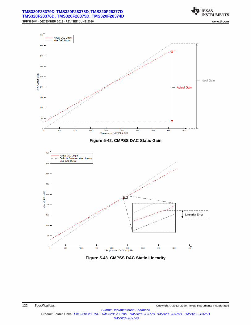
Linearity Error
Actual Linear Range
Ideal Gain
Actual Gain
122
TMS320F28379D, TMS320F28378D, TMS320F28377DTMS320F28376D, TMS320F28375D, TMS320F28374DSPRS880M –DECEMBER 2013–REVISED JUNE 2020 www.ti.com
Submit Documentation FeedbackProduct Folder Links: TMS320F28379D TMS320F28378D TMS320F28377D TMS320F28376D TMS320F28375D
TMS320F28374D
Specifications Copyright © 2013–2020, Texas Instruments Incorporated
Figure 5-42. CMPSS DAC Static Gain
Figure 5-43. CMPSS DAC Static Linearity
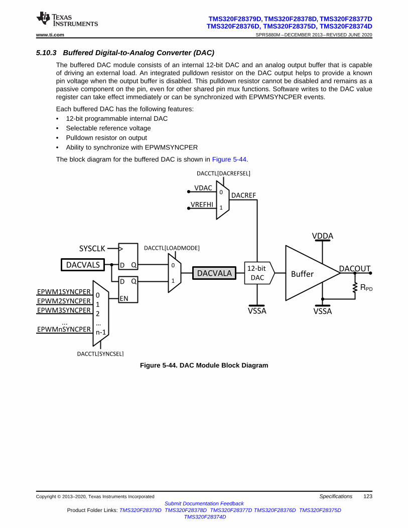
EPWM1SYNCPER
VREFHI
VDDA
VSSA
VDAC
DACCTL[DACREFSEL]
DACCTL[LOADMODE]SYSCLK
DACCTL[SYNCSEL]
EPWM2SYNCPER
EPWM3SYNCPER
EPWMnSYNCPER...
0
1
D Q
>
D Q
DACVALS
0
1
2
Y
n-1
0
1
DACVALA Buffer12-bit
DAC
VSSA
DACOUT
DACREF
RPD
EN
123
TMS320F28379D, TMS320F28378D, TMS320F28377DTMS320F28376D, TMS320F28375D, TMS320F28374D
www.ti.com SPRS880M –DECEMBER 2013–REVISED JUNE 2020
Submit Documentation FeedbackProduct Folder Links: TMS320F28379D TMS320F28378D TMS320F28377D TMS320F28376D TMS320F28375D
TMS320F28374D
SpecificationsCopyright © 2013–2020, Texas Instruments Incorporated
5.10.3 Buffered Digital-to-Analog Converter (DAC)The buffered DAC module consists of an internal 12-bit DAC and an analog output buffer that is capableof driving an external load. An integrated pulldown resistor on the DAC output helps to provide a knownpin voltage when the output buffer is disabled. This pulldown resistor cannot be disabled and remains as apassive component on the pin, even for other shared pin mux functions. Software writes to the DAC valueregister can take effect immediately or can be synchronized with EPWMSYNCPER events.
Each buffered DAC has the following features:• 12-bit programmable internal DAC• Selectable reference voltage• Pulldown resistor on output• Ability to synchronize with EPWMSYNCPER
The block diagram for the buffered DAC is shown in Figure 5-44.
Figure 5-44. DAC Module Block Diagram

124
TMS320F28379D, TMS320F28378D, TMS320F28377DTMS320F28376D, TMS320F28375D, TMS320F28374DSPRS880M –DECEMBER 2013–REVISED JUNE 2020 www.ti.com
Submit Documentation FeedbackProduct Folder Links: TMS320F28379D TMS320F28378D TMS320F28377D TMS320F28376D TMS320F28375D
TMS320F28374D
Specifications Copyright © 2013–2020, Texas Instruments Incorporated
5.10.3.1 Buffered DAC Electrical Data and Timing
Table 5-56 shows the buffered DAC electrical characteristics. Figure 5-45 shows the buffered DAC offset.Figure 5-46 shows the buffered DAC gain. Figure 5-47 shows the buffered DAC linearity.
(1) Typical values are measured with VREFHI = 3.3 V unless otherwise noted. Minimum and Maximum values are tested or characterizedwith VREFHI = 2.5 V.
(2) See the "Analog Bandgap References" advisory of the TMS320F2837xD Dual-Core MCUs Silicon Errata.(3) Gain error is calculated for linear output range.(4) The DAC output is monotonic.(5) This is the linear output range of the DAC. The DAC can generate voltages outside this range, but the output voltage will not be linear
due to the buffer.(6) For best PSRR performance, VDAC or VREFHI should be less than VDDA.(7) Per active Buffered DAC module.(8) VREFHI = 3.2 V, VDDA = 3.3 V DC + 100 mV Sine.
Table 5-56. Buffered DAC Electrical Characteristicsover recommended operating conditions (unless otherwise noted) (1)
PARAMETER TEST CONDITIONS MIN TYP MAX UNITPower-up time 500 (2) µsOffset error Midpoint –10 10 mVGain error (3) –2.5 2.5 % of FSRDNL (4) Endpoint corrected > –1 ±0.4 1 LSBINL Endpoint corrected –5 ±2 5 LSB
DACOUTx settling time Settling to 2 LSBs after 0.3V-to-3Vtransition 2 µs
Resolution 12 bitsVoltage output range (5) 0.3 VDDA – 0.3 VCapacitive load Output drive capability 100 pFResistive load Output drive capability 5 kΩRPD pulldown resistor 50 kΩReference voltage (6) VDAC or VREFHI 2.4 2.5 or 3.0 VDDA VReference input resistance (7) VDAC or VREFHI 170 kΩ
Output noiseIntegrated noise from 100 Hz to 100 kHz 500 µVrmsNoise density at 10 kHz 711 nVrms/√Hz
Glitch energy 1.5 V-ns
PSRR (8) DC up to 1 kHz 70dB
100 kHz 30SNR 1020 Hz 67 dBTHD 1020 Hz –63 dB
SFDR1020 Hz, including harmonics and spurs 66
dBc1020 Hz, including only spurs 104
NOTEThe VDAC pin must be kept below VDDA + 0.3 V to ensure proper functional operation. If theVDAC pin exceeds this level, a blocking circuit may activate, and the internal value of VDACmay float to 0 V internally, giving improper DAC output.

Offset Error
Code 2048
125
TMS320F28379D, TMS320F28378D, TMS320F28377DTMS320F28376D, TMS320F28375D, TMS320F28374D
www.ti.com SPRS880M –DECEMBER 2013–REVISED JUNE 2020
Submit Documentation FeedbackProduct Folder Links: TMS320F28379D TMS320F28378D TMS320F28377D TMS320F28376D TMS320F28375D
TMS320F28374D
SpecificationsCopyright © 2013–2020, Texas Instruments Incorporated
NOTEThe VREFHI pin must be kept below VDDA + 0.3 V to ensure proper functional operation. If theVREFHI pin exceeds this level, a blocking circuit may activate, and the internal value of VREFHImay float to 0 V internally, giving improper ADC conversion or DAC output.
Figure 5-45. Buffered DAC Offset

Linearity Error
Code 3722Code 373
Linear Range
(3.3-V Reference)
Code 3722Code 373
Actual Gain
Ideal Gain
Linear Range
(3.3-V Reference)
126
TMS320F28379D, TMS320F28378D, TMS320F28377DTMS320F28376D, TMS320F28375D, TMS320F28374DSPRS880M –DECEMBER 2013–REVISED JUNE 2020 www.ti.com
Submit Documentation FeedbackProduct Folder Links: TMS320F28379D TMS320F28378D TMS320F28377D TMS320F28376D TMS320F28375D
TMS320F28374D
Specifications Copyright © 2013–2020, Texas Instruments Incorporated
Figure 5-46. Buffered DAC Gain
Figure 5-47. Buffered DAC Linearity

127
TMS320F28379D, TMS320F28378D, TMS320F28377DTMS320F28376D, TMS320F28375D, TMS320F28374D
www.ti.com SPRS880M –DECEMBER 2013–REVISED JUNE 2020
Submit Documentation FeedbackProduct Folder Links: TMS320F28379D TMS320F28378D TMS320F28377D TMS320F28376D TMS320F28375D
TMS320F28374D
SpecificationsCopyright © 2013–2020, Texas Instruments Incorporated
5.11 Control Peripherals
NOTEFor the actual number of each peripheral on a specific device, see Table 3-1.
5.11.1 Enhanced Capture (eCAP)The eCAP module can be used in systems where accurate timing of external events is important.
Applications for eCAP include:• Speed measurements of rotating machinery (for example, toothed sprockets sensed through Hall
sensors)• Elapsed time measurements between position sensor pulses• Period and duty cycle measurements of pulse train signals• Decoding current or voltage amplitude derived from duty cycle encoded current/voltage sensors
The eCAP module includes the following features:• 4-event time-stamp registers (each 32 bits)• Edge-polarity selection for up to four sequenced time-stamp capture events• Interrupt on either of the four events• Single shot capture of up to four event timestamps• Continuous mode capture of timestamps in a four-deep circular buffer• Absolute time-stamp capture• Difference (Delta) mode time-stamp capture• All of the above resources dedicated to a single input pin• When not used in capture mode, the eCAP module can be configured as a single-channel PWM output
(APWM).
The eCAP inputs connect to any GPIO input through the Input X-BAR. The APWM outputs connect toGPIO pins through the Output X-BAR to OUTPUTx positions in the GPIO mux. See Section 4.4.2 andSection 4.4.3.
Figure 5-48 shows the block diagram of an eCAP module.

TSCTR(counter−32 bit)
RST
CAP1(APRD active)
LD
CAP2(ACMP active)
LD
CAP3(APRD shadow)
LD
CAP4(ACMP shadow)
LD
Continuous /Oneshot
Capture Control
LD1
LD2
LD3
LD4
32
32
PRD [0−31]
CMP [0−31]
CTR [0−31]
eCAPx
InterruptTrigger
andFlag
control
to PIE
CTR=CMP
32
32
32
32
32
ACMPshadow
Event
Prescale
CTRPHS(phase register−32 bit)
SYNCOut
SYNCIn
Eventqualifier
Polarityselect
Polarityselect
Polarityselect
Polarityselect
CTR=PRD
CTR_OVF
4
PWMcompare
logic
CTR [0−31]
PRD [0−31]
CMP [0−31]
CTR=CMP
CTR=PRD
CTR_OVFOVF
APWM mode
Delta−mode
SY
NC
4Capture events
CEVT[1:4]
APRDshadow
32
32 MO
DE
SE
LE
CT
128
TMS320F28379D, TMS320F28378D, TMS320F28377DTMS320F28376D, TMS320F28375D, TMS320F28374DSPRS880M –DECEMBER 2013–REVISED JUNE 2020 www.ti.com
Submit Documentation FeedbackProduct Folder Links: TMS320F28379D TMS320F28378D TMS320F28377D TMS320F28376D TMS320F28375D
TMS320F28374D
Specifications Copyright © 2013–2020, Texas Instruments Incorporated
Figure 5-48. eCAP Block Diagram
The eCAP module is clocked by PERx.SYSCLK.
The clock enable bits (ECAP1–ECAP6) in the PCLKCR3 register turn off the eCAP module individually(for low-power operation). Upon reset, ECAP1ENCLK is set to low, indicating that the peripheral clockis off.

129
TMS320F28379D, TMS320F28378D, TMS320F28377DTMS320F28376D, TMS320F28375D, TMS320F28374D
www.ti.com SPRS880M –DECEMBER 2013–REVISED JUNE 2020
Submit Documentation FeedbackProduct Folder Links: TMS320F28379D TMS320F28378D TMS320F28377D TMS320F28376D TMS320F28375D
TMS320F28374D
SpecificationsCopyright © 2013–2020, Texas Instruments Incorporated
5.11.1.1 eCAP Electrical Data and Timing
Table 5-57 shows the eCAP timing requirement and Table 5-58 shows the eCAP switching characteristics.
(1) For an explanation of the input qualifier parameters, see Table 5-24.
Table 5-57. eCAP Timing Requirement (1)
MIN MAX UNIT
tw(CAP) Capture input pulse widthAsynchronous 2tc(SYSCLK) cyclesSynchronous 2tc(SYSCLK) cyclesWith input qualifier 1tc(SYSCLK) + tw(IQSW) cycles
Table 5-58. eCAP Switching Characteristicsover recommended operating conditions (unless otherwise noted)
PARAMETER MIN MAX UNITtw(APWM) Pulse duration, APWMx output high/low 20 ns

130
TMS320F28379D, TMS320F28378D, TMS320F28377DTMS320F28376D, TMS320F28375D, TMS320F28374DSPRS880M –DECEMBER 2013–REVISED JUNE 2020 www.ti.com
Submit Documentation FeedbackProduct Folder Links: TMS320F28379D TMS320F28378D TMS320F28377D TMS320F28376D TMS320F28375D
TMS320F28374D
Specifications Copyright © 2013–2020, Texas Instruments Incorporated
5.11.2 Enhanced Pulse Width Modulator (ePWM)The ePWM peripheral is a key element in controlling many of the power electronic systems found in bothcommercial and industrial equipment. The ePWM type-4 module is able to generate complex pulse widthwaveforms with minimal CPU overhead by building the peripheral up from smaller modules with separateresources that can operate together to form a system. Some of the highlights of the ePWM type-4 moduleinclude complex waveform generation, dead-band generation, a flexible synchronization scheme,advanced trip-zone functionality, and global register reload capabilities.
Figure 5-49 shows the signal interconnections with the ePWM. Figure 5-50 shows the ePWM trip inputconnectivity.

TBPRD Shadow (24)
TBPRD Active (24)
CounterUp/Down(16 Bit)
TBCTRActive (16)
TBCTL[PHSEN]
CTR=PRD
16
PhaseControl
8
CTR=ZERO
CTR_Dir
TBPHSHR (8)
TBPRDHR (8)
8
Time-Base (TB)
TBPHS Active (24)
CTR=PRD
CTR=ZERO
CTR_Dir
DCAEVT1.soc(A)
DCBEVT1.soc(A)
EventTrigger
andInterrupt
(ET)
EPWMx_INT
ADCSOCAO
ADCSOCBO
EPWMxSOCA On-chipADC
ActionQualifier
(AQ)
EPWMA
EPWMB
DeadBand(DB)
PWMChopper
(PC)
TripZone(TZ)
ePWMxA
ePWMxB
CTR=ZERO
EPWMx_TZ_INT
TZ1 TZ3to
EMUSTOP
CLOCKFAIL
EQEPxERR
DCAEVT1.force(A)
DCAEVT2.force(A)
DCBEVT1.force(A)
DCBEVT2.force(A)
CTR=CMPA
16
CMPAHR (8)
CTR=CMPB
16
CMPB Active (24)
CMPB Shadow (24)
HiRes PWM (HRPWM)
CTR=PRD or ZERO
DCAEVT1.inter
DCBEVT1.inter
DCAEVT2.inter
DCBEVT2.inter
CMPA Active (24)
CMPA Shadow (24)
CTR=CMPB
CTR=CMPC
CTR=CMPA
CTR=CMPD
CMPBHR (8)
CMPAHR (8)
CMPBHR (8)
CTR=CMPC
16
TBCNT(16)
CMPC[15-0]
CTR=CMPD
16
TBCNT(16)
CMPD[15-0]
Counter Compare (CC)
CMPD Active (16)
CMPD Shadow (16)
CMPC Active (16)
CMPC Shadow (16)
SyncOut
Select
CTR=ZERO
CTR=CMPB
EPWMxSYNCO
EPWMxSYNCI
TBCTL[SWFSYNC]
TBCTL[SYNCOSEL]
00
01
10
11
TBCTL2[SYNCOSELX]
Disable
CTR=CMPC
CTR=CMPDRsvd
EPWMxSOCB
DCBEVT1.sync(A)
DCAEVT1.sync(A)
Select and pulse stretchfor external ADC
ADCSOCOUTSELECT
Copyright © 2017, Texas Instruments Incorporated
131
TMS320F28379D, TMS320F28378D, TMS320F28377DTMS320F28376D, TMS320F28375D, TMS320F28374D
www.ti.com SPRS880M –DECEMBER 2013–REVISED JUNE 2020
Submit Documentation FeedbackProduct Folder Links: TMS320F28379D TMS320F28378D TMS320F28377D TMS320F28376D TMS320F28375D
TMS320F28374D
SpecificationsCopyright © 2013–2020, Texas Instruments Incorporated
A. These events are generated by the ePWM digital compare (DC) submodule based on the levels of the TRIPIN inputs.
Figure 5-49. ePWM Submodules and Critical Internal Signal Interconnects

132
TMS320F28379D, TMS320F28378D, TMS320F28377DTMS320F28376D, TMS320F28375D, TMS320F28374DSPRS880M –DECEMBER 2013–REVISED JUNE 2020 www.ti.com
Submit Documentation FeedbackProduct Folder Links: TMS320F28379D TMS320F28378D TMS320F28377D TMS320F28376D TMS320F28375D
TMS320F28374D
Specifications Copyright © 2013–2020, Texas Instruments Incorporated
Figure 5-50. ePWM Trip Input Connectivity

EPWM1
EPWM2
EPWM3 EPWM4
EPWM5
EPWM6EPWM7
EPWM8
EPWM9EPWM10
EPWM11
EPWM12 ECAP1
EXTSYNCIN1
EXTSYNCOUT
Pulse-Stretched
(8 PLLSYSCLK
Cycles)
SYNCSEL.EPWM4SYNCIN
EXTSYNCIN2
SYNCSEL.SYNCOUT
SYNCSEL.EPWM7SYNCIN
SYNCSEL.ECAP4SYNCIN
SYNCSEL.ECAP1SYNCIN
SYNCSEL.EPWM10SYNCIN
EPWM1SYNCOUT
EPWM4SYNCOUT
EPWM7SYNCOUT
EPWM10SYNCOUT
ECAP1SYNCOUT
ECAP2
ECAP3ECAP4
ECAP5
ECAP6
133
TMS320F28379D, TMS320F28378D, TMS320F28377DTMS320F28376D, TMS320F28375D, TMS320F28374D
www.ti.com SPRS880M –DECEMBER 2013–REVISED JUNE 2020
Submit Documentation FeedbackProduct Folder Links: TMS320F28379D TMS320F28378D TMS320F28377D TMS320F28376D TMS320F28375D
TMS320F28374D
SpecificationsCopyright © 2013–2020, Texas Instruments Incorporated
5.11.2.1 Control Peripherals Synchronization
The ePWM and eCAP synchronization chain on the device provides flexibility in partitioning the ePWMand eCAP modules between CPU1 and CPU2 and allows localized synchronization within the modulesbelonging to the same CPU. Like the other peripherals, the partitioning of the ePWM and eCAP modulesneeds to be done using the CPUSELx registers. Figure 5-51 shows the synchronization chain architecture.
Figure 5-51. Synchronization Chain Architecture
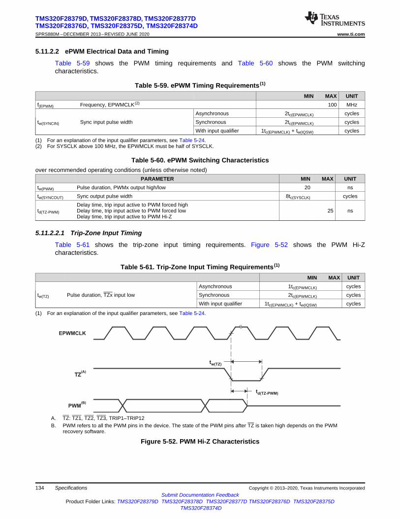
PWM(B)
TZ(A)
EPWMCLK
tw(TZ)
td(TZ-PWM)
134
TMS320F28379D, TMS320F28378D, TMS320F28377DTMS320F28376D, TMS320F28375D, TMS320F28374DSPRS880M –DECEMBER 2013–REVISED JUNE 2020 www.ti.com
Submit Documentation FeedbackProduct Folder Links: TMS320F28379D TMS320F28378D TMS320F28377D TMS320F28376D TMS320F28375D
TMS320F28374D
Specifications Copyright © 2013–2020, Texas Instruments Incorporated
5.11.2.2 ePWM Electrical Data and Timing
Table 5-59 shows the PWM timing requirements and Table 5-60 shows the PWM switchingcharacteristics.
(1) For an explanation of the input qualifier parameters, see Table 5-24.(2) For SYSCLK above 100 MHz, the EPWMCLK must be half of SYSCLK.
Table 5-59. ePWM Timing Requirements (1)
MIN MAX UNITf(EPWM) Frequency, EPWMCLK (2) 100 MHz
tw(SYNCIN) Sync input pulse widthAsynchronous 2tc(EPWMCLK) cyclesSynchronous 2tc(EPWMCLK) cyclesWith input qualifier 1tc(EPWMCLK) + tw(IQSW) cycles
Table 5-60. ePWM Switching Characteristicsover recommended operating conditions (unless otherwise noted)
PARAMETER MIN MAX UNITtw(PWM) Pulse duration, PWMx output high/low 20 nstw(SYNCOUT) Sync output pulse width 8tc(SYSCLK) cycles
td(TZ-PWM)
Delay time, trip input active to PWM forced highDelay time, trip input active to PWM forced lowDelay time, trip input active to PWM Hi-Z
25 ns
5.11.2.2.1 Trip-Zone Input Timing
Table 5-61 shows the trip-zone input timing requirements. Figure 5-52 shows the PWM Hi-Zcharacteristics.
(1) For an explanation of the input qualifier parameters, see Table 5-24.
Table 5-61. Trip-Zone Input Timing Requirements (1)
MIN MAX UNIT
tw(TZ) Pulse duration, TZx input lowAsynchronous 1tc(EPWMCLK) cyclesSynchronous 2tc(EPWMCLK) cyclesWith input qualifier 1tc(EPWMCLK) + tw(IQSW) cycles
A. TZ: TZ1, TZ2, TZ3, TRIP1–TRIP12B. PWM refers to all the PWM pins in the device. The state of the PWM pins after TZ is taken high depends on the PWM
recovery software.
Figure 5-52. PWM Hi-Z Characteristics

ADCSOCAO
ADCSOCBOor
tw(ADCSOCL)
135
TMS320F28379D, TMS320F28378D, TMS320F28377DTMS320F28376D, TMS320F28375D, TMS320F28374D
www.ti.com SPRS880M –DECEMBER 2013–REVISED JUNE 2020
Submit Documentation FeedbackProduct Folder Links: TMS320F28379D TMS320F28378D TMS320F28377D TMS320F28376D TMS320F28375D
TMS320F28374D
SpecificationsCopyright © 2013–2020, Texas Instruments Incorporated
5.11.2.3 External ADC Start-of-Conversion Electrical Data and Timing
Table 5-62 shows the external ADC start-of-conversion switching characteristics. Figure 5-53 shows theADCSOCAO or ADCSOCBO timing.
Table 5-62. External ADC Start-of-Conversion Switching Characteristicsover recommended operating conditions (unless otherwise noted)
PARAMETER MIN MAX UNITtw(ADCSOCL) Pulse duration, ADCSOCxO low 32tc(SYSCLK) cycles
Figure 5-53. ADCSOCAO or ADCSOCBO Timing
136
TMS320F28379D, TMS320F28378D, TMS320F28377DTMS320F28376D, TMS320F28375D, TMS320F28374DSPRS880M –DECEMBER 2013–REVISED JUNE 2020 www.ti.com
Submit Documentation FeedbackProduct Folder Links: TMS320F28379D TMS320F28378D TMS320F28377D TMS320F28376D TMS320F28375D
TMS320F28374D
Specifications Copyright © 2013–2020, Texas Instruments Incorporated
5.11.3 Enhanced Quadrature Encoder Pulse (eQEP)The eQEP module interfaces directly with linear or rotary incremental encoders to obtain position,direction, and speed information from rotating machines used in high-performance motion and position-control systems.
Each eQEP peripheral comprises five major functional blocks:• Quadrature Capture Unit (QCAP)• Position Counter/Control Unit (PCCU)• Quadrature Decoder Unit (QDU)• Unit Time Base for speed and frequency measurement (UTIME)• Watchdog timer for detecting stalls (QWDOG)
The eQEP peripherals are clocked by PERx.SYSCLK. Figure 5-54 shows the eQEP block diagram.
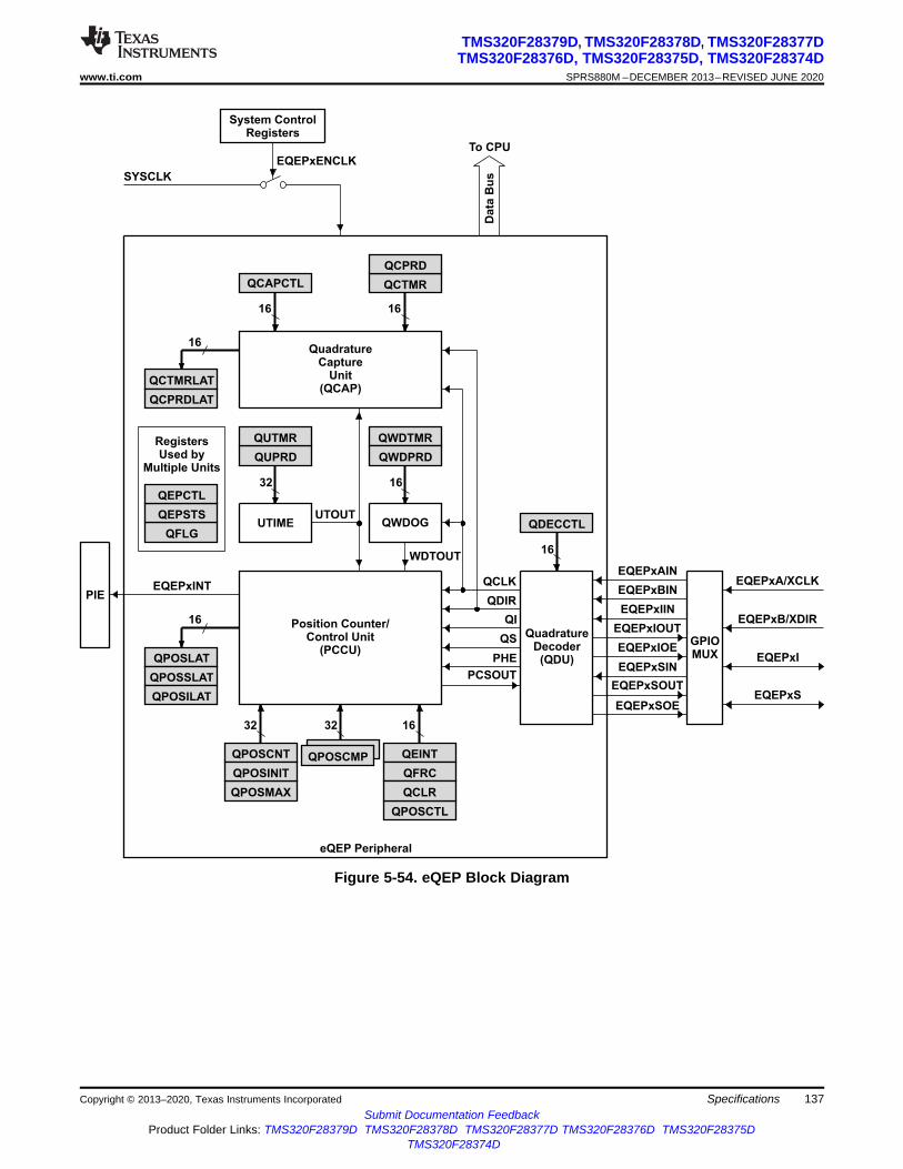
QWDTMR
QWDPRD
16
QWDOGUTIME
QUPRD
QUTMR
32
UTOUT
WDTOUT
QuadratureCapture
Unit(QCAP)
QCPRDLAT
QCTMRLAT
16
QFLG
QEPSTS
QEPCTL
RegistersUsed by
Multiple Units
QCLK
QDIR
QI
QS
PHE
PCSOUT
QuadratureDecoder
(QDU)
QDECCTL
16
Position Counter/Control Unit
(PCCU)QPOSLAT
QPOSSLAT
16
QPOSILAT
EQEPxAIN
EQEPxBIN
EQEPxIIN
EQEPxIOUT
EQEPxIOE
EQEPxSIN
EQEPxSOUT
EQEPxSOE
GPIOMUX
EQEPxA/XCLK
EQEPxB/XDIR
EQEPxS
EQEPxI
QPOSCMP QEINT
QFRC
32
QCLR
QPOSCTL
1632
QPOSCNT
QPOSMAX
QPOSINIT
PIEEQEPxINT
eQEP Peripheral
System ControlRegisters
QCTMR
QCPRD
1616
QCAPCTL
EQEPxENCLK
SYSCLK
To CPU
Da
ta B
us
137
TMS320F28379D, TMS320F28378D, TMS320F28377DTMS320F28376D, TMS320F28375D, TMS320F28374D
www.ti.com SPRS880M –DECEMBER 2013–REVISED JUNE 2020
Submit Documentation FeedbackProduct Folder Links: TMS320F28379D TMS320F28378D TMS320F28377D TMS320F28376D TMS320F28375D
TMS320F28374D
SpecificationsCopyright © 2013–2020, Texas Instruments Incorporated
Figure 5-54. eQEP Block Diagram

138
TMS320F28379D, TMS320F28378D, TMS320F28377DTMS320F28376D, TMS320F28375D, TMS320F28374DSPRS880M –DECEMBER 2013–REVISED JUNE 2020 www.ti.com
Submit Documentation FeedbackProduct Folder Links: TMS320F28379D TMS320F28378D TMS320F28377D TMS320F28376D TMS320F28375D
TMS320F28374D
Specifications Copyright © 2013–2020, Texas Instruments Incorporated
5.11.3.1 eQEP Electrical Data and Timing
Table 5-63 lists the eQEP timing requirement and Table 5-64 lists the eQEP switching characteristics.
(1) For an explanation of the input qualifier parameters, see Table 5-24.(2) See the TMS320F2837xD Dual-Core MCUs Silicon Errata for limitations in the asynchronous mode.
Table 5-63. eQEP Timing Requirements (1)
MIN MAX UNIT
tw(QEPP) QEP input periodAsynchronous (2)/Synchronous 2tc(SYSCLK) cyclesWith input qualifier 2[1tc(SYSCLK) + tw(IQSW)] cycles
tw(INDEXH) QEP Index Input High timeAsynchronous (2)/Synchronous 2tc(SYSCLK) cyclesWith input qualifier 2tc(SYSCLK) + tw(IQSW) cycles
tw(INDEXL) QEP Index Input Low timeAsynchronous (2)/Synchronous 2tc(SYSCLK) cyclesWith input qualifier 2tc(SYSCLK) + tw(IQSW) cycles
tw(STROBH) QEP Strobe High timeAsynchronous (2)/Synchronous 2tc(SYSCLK) cyclesWith input qualifier 2tc(SYSCLK) + tw(IQSW) cycles
tw(STROBL) QEP Strobe Input Low timeAsynchronous (2)/Synchronous 2tc(SYSCLK) cyclesWith input qualifier 2tc(SYSCLK) + tw(IQSW) cycles
Table 5-64. eQEP Switching Characteristicsover recommended operating conditions (unless otherwise noted)
PARAMETER MIN MAX UNITtd(CNTR)xin Delay time, external clock to counter increment 4tc(SYSCLK) cyclestd(PCS-OUT)QEP Delay time, QEP input edge to position compare sync output 6tc(SYSCLK) cycles

139
TMS320F28379D, TMS320F28378D, TMS320F28377DTMS320F28376D, TMS320F28375D, TMS320F28374D
www.ti.com SPRS880M –DECEMBER 2013–REVISED JUNE 2020
Submit Documentation FeedbackProduct Folder Links: TMS320F28379D TMS320F28378D TMS320F28377D TMS320F28376D TMS320F28375D
TMS320F28374D
SpecificationsCopyright © 2013–2020, Texas Instruments Incorporated
5.11.4 High-Resolution Pulse Width Modulator (HRPWM)The HRPWM combines multiple delay lines in a single module and a simplified calibration system by usinga dedicated calibration delay line. For each ePWM module, there are two HR outputs:• HR Duty and Deadband control on Channel A• HR Duty and Deadband control on Channel B
The HRPWM module offers PWM resolution (time granularity) that is significantly better than what can beachieved using conventionally derived digital PWM methods. The key points for the HRPWM module are:• Significantly extends the time resolution capabilities of conventionally derived digital PWM• This capability can be used in both single edge (duty cycle and phase-shift control) as well as dual
edge control for frequency/period modulation.• Finer time granularity control or edge positioning is controlled through extensions to the Compare A, B,
phase, period and deadband registers of the ePWM module.
NOTEThe minimum HRPWMCLK frequency allowed for HRPWM is 60 MHz.
5.11.4.1 HRPWM Electrical Data and Timing
Table 5-65 lists the high-resolution PWM timing requirements. Table 5-66 lists the high-resolution PWMswitching characteristics.
(1) For SYSCLK above 100 MHz, the EPWMCLK must be half of SYSCLK.
Table 5-65. High-Resolution PWM Timing RequirementsMIN MAX UNIT
f(EPWM) Frequency, EPWMCLK (1) 100 MHzf(HRPWM) Frequency, HRPWMCLK 60 100 MHz
(1) The MEP step size will be largest at high temperature and minimum voltage on VDD. MEP step size will increase with highertemperature and lower voltage and decrease with lower temperature and higher voltage.Applications that use the HRPWM feature should use MEP Scale Factor Optimizer (SFO) estimation software functions. See the TIsoftware libraries for details of using SFO functions in end applications. SFO functions help to estimate the number of MEP steps perSYSCLK period dynamically while the HRPWM is in operation.
Table 5-66. High-Resolution PWM CharacteristicsPARAMETER MIN TYP MAX UNIT
Micro Edge Positioning (MEP) step size (1) 150 310 ps

140
TMS320F28379D, TMS320F28378D, TMS320F28377DTMS320F28376D, TMS320F28375D, TMS320F28374DSPRS880M –DECEMBER 2013–REVISED JUNE 2020 www.ti.com
Submit Documentation FeedbackProduct Folder Links: TMS320F28379D TMS320F28378D TMS320F28377D TMS320F28376D TMS320F28375D
TMS320F28374D
Specifications Copyright © 2013–2020, Texas Instruments Incorporated
5.11.5 Sigma-Delta Filter Module (SDFM)The SDFM is a four-channel digital filter designed specifically for current measurement and resolverposition decoding in motor control applications. Each channel can receive an independent sigma-delta(ΣΔ) modulated bit stream. The bit streams are processed by four individually programmable digitaldecimation filters. The filter set includes a fast comparator for immediate digital threshold comparisons forovercurrent and undercurrent monitoring. Figure 5-55 shows a block diagram of the SDFMs.
SDFM features include:• Eight external pins per SDFM module:
– Four sigma-delta data input pins per SDFM module (SDx_Dy, where x = 1 to 2 and y = 1 to 4)– Four sigma-delta clock input pins per SDFM module (SDx_Cy, where x = 1 to 2 and y = 1 to 4)
• Four different configurable modulator clock modes:– Modulator clock rate equals modulator data rate– Modulator clock rate running at half the modulator data rate– Modulator data is Manchester encoded. Modulator clock not required.– Modulator clock rate is double that of modulator data rate
• Four independent configurable comparator units:– Four different filter type selection (Sinc1/Sinc2/Sincfast/Sinc3) options available– Ability to detect over-value and under-value conditions– Comparator Over-Sampling Ratio (COSR) value for comparator programmable from 1 to 32
• Four independent configurable data filter units:– Four different filter type selection (Sinc1/Sinc2/Sincfast/Sinc3) options available– Data filter Over-Sampling Ratio (DOSR) value for data filter unit programmable from 1 to 256– Ability to enable or disable individual filter module– Ability to synchronize all four independent filters of a SDFM module using the Master Filter Enable
(MFE) bit or the PWM signals.• Filter data can be 16-bit or 32-bit representation• PWMs can be used to generate modulator clock for sigma-delta modulators
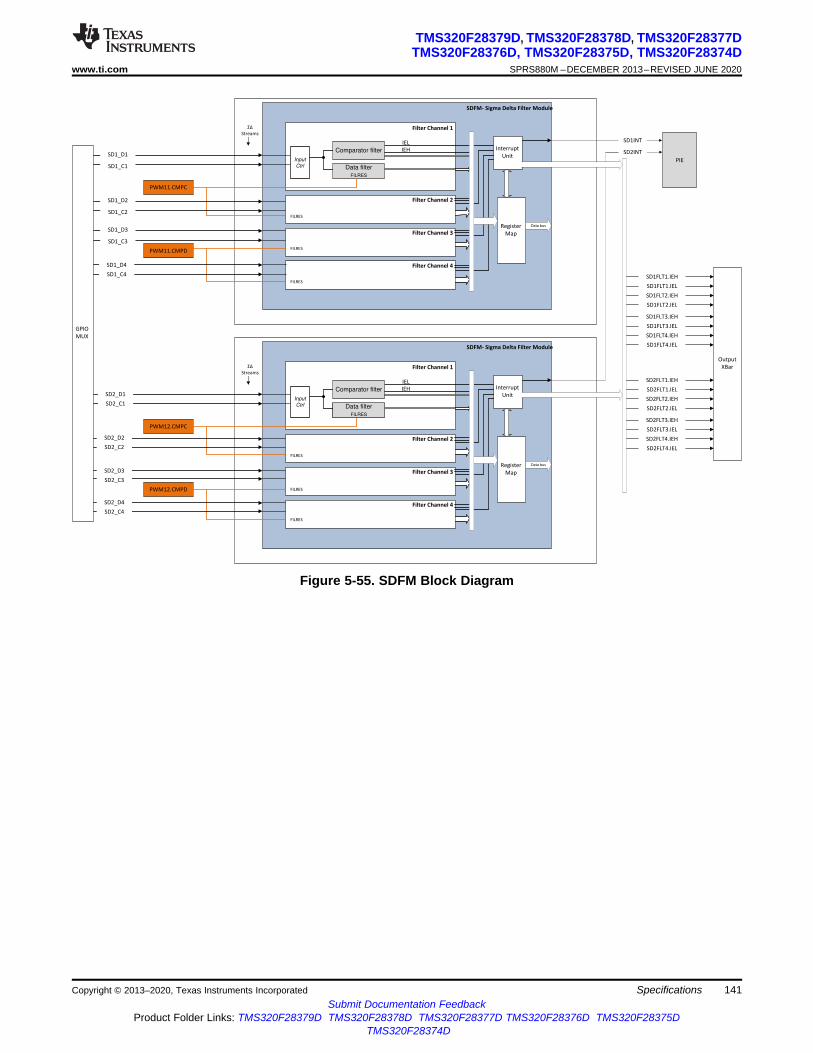
Filter Channel 1
SDFM- Sigma Delta Filter Module
Input
Ctrl
G4
Streams
Data busRegister
Map
R
R
Comparator filter
Data filter
FILRES
Filter Channel 4
Filter Channel 3
Filter Channel 2
PIE
Interrupt
Unit
IEL
IEH
SD1INT
Filter Channel 1
SDFM- Sigma Delta Filter Module
Input
Ctrl
G4
Streams
Data busRegister
Map
R
R
Comparator filter
Data filter
Filter Channel 4
Filter Channel 3
Filter Channel 2
Interrupt
Unit
IEL
IEH
SD2INT
Output
XBar
SD1FLT1.IEH
SD1FLT1.IEL
SD1FLT2.IEH
SD1FLT2.IEL
SD1FLT3.IEH
SD1FLT3.IEL
SD1FLT4.IEH
SD1FLT4.IEL
SD2FLT1.IEH
SD2FLT1.IEL
SD2FLT2.IEH
SD2FLT2.IEL
SD2FLT3.IEH
SD2FLT3.IEL
SD2FLT4.IEH
SD2FLT4.IEL
PWM11.CMPC
PWM11.CMPD
FILRES
FILRES
FILRES
PWM12.CMPC
FILRES
PWM12.CMPD FILRES
FILRES
Data filter
FILRES
GPIO
MUX
SD2_D1
SD2_C1
SD2_D2
SD2_C2
SD2_D3
SD2_C3
SD2_D4
SD2_C4
SD1_D4
SD1_C4
SD1_D3
SD1_C3
SD1_D2
SD1_C2
SD1_D1
SD1_C1
141
TMS320F28379D, TMS320F28378D, TMS320F28377DTMS320F28376D, TMS320F28375D, TMS320F28374D
www.ti.com SPRS880M –DECEMBER 2013–REVISED JUNE 2020
Submit Documentation FeedbackProduct Folder Links: TMS320F28379D TMS320F28378D TMS320F28377D TMS320F28376D TMS320F28375D
TMS320F28374D
SpecificationsCopyright © 2013–2020, Texas Instruments Incorporated
Figure 5-55. SDFM Block Diagram
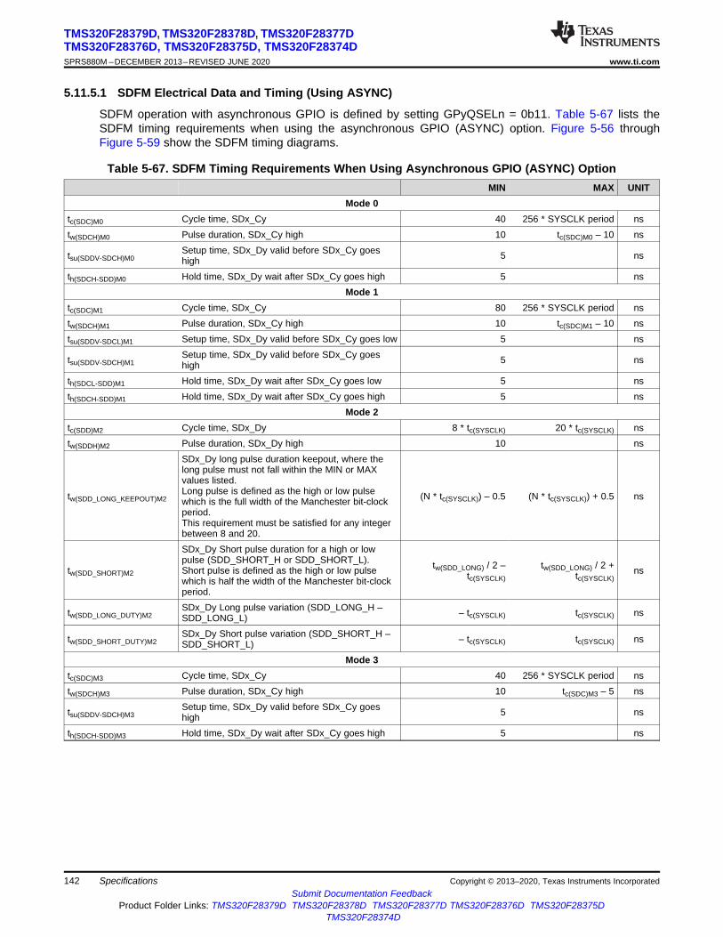
142
TMS320F28379D, TMS320F28378D, TMS320F28377DTMS320F28376D, TMS320F28375D, TMS320F28374DSPRS880M –DECEMBER 2013–REVISED JUNE 2020 www.ti.com
Submit Documentation FeedbackProduct Folder Links: TMS320F28379D TMS320F28378D TMS320F28377D TMS320F28376D TMS320F28375D
TMS320F28374D
Specifications Copyright © 2013–2020, Texas Instruments Incorporated
5.11.5.1 SDFM Electrical Data and Timing (Using ASYNC)
SDFM operation with asynchronous GPIO is defined by setting GPyQSELn = 0b11. Table 5-67 lists theSDFM timing requirements when using the asynchronous GPIO (ASYNC) option. Figure 5-56 throughFigure 5-59 show the SDFM timing diagrams.
Table 5-67. SDFM Timing Requirements When Using Asynchronous GPIO (ASYNC) OptionMIN MAX UNIT
Mode 0tc(SDC)M0 Cycle time, SDx_Cy 40 256 * SYSCLK period nstw(SDCH)M0 Pulse duration, SDx_Cy high 10 tc(SDC)M0 – 10 ns
tsu(SDDV-SDCH)M0Setup time, SDx_Dy valid before SDx_Cy goeshigh 5 ns
th(SDCH-SDD)M0 Hold time, SDx_Dy wait after SDx_Cy goes high 5 nsMode 1
tc(SDC)M1 Cycle time, SDx_Cy 80 256 * SYSCLK period nstw(SDCH)M1 Pulse duration, SDx_Cy high 10 tc(SDC)M1 – 10 nstsu(SDDV-SDCL)M1 Setup time, SDx_Dy valid before SDx_Cy goes low 5 ns
tsu(SDDV-SDCH)M1Setup time, SDx_Dy valid before SDx_Cy goeshigh 5 ns
th(SDCL-SDD)M1 Hold time, SDx_Dy wait after SDx_Cy goes low 5 nsth(SDCH-SDD)M1 Hold time, SDx_Dy wait after SDx_Cy goes high 5 ns
Mode 2tc(SDD)M2 Cycle time, SDx_Dy 8 * tc(SYSCLK) 20 * tc(SYSCLK) nstw(SDDH)M2 Pulse duration, SDx_Dy high 10 ns
tw(SDD_LONG_KEEPOUT)M2
SDx_Dy long pulse duration keepout, where thelong pulse must not fall within the MIN or MAXvalues listed.Long pulse is defined as the high or low pulsewhich is the full width of the Manchester bit-clockperiod.This requirement must be satisfied for any integerbetween 8 and 20.
(N * tc(SYSCLK)) – 0.5 (N * tc(SYSCLK)) + 0.5 ns
tw(SDD_SHORT)M2
SDx_Dy Short pulse duration for a high or lowpulse (SDD_SHORT_H or SDD_SHORT_L).Short pulse is defined as the high or low pulsewhich is half the width of the Manchester bit-clockperiod.
tw(SDD_LONG) / 2 –tc(SYSCLK)
tw(SDD_LONG) / 2 +tc(SYSCLK)
ns
tw(SDD_LONG_DUTY)M2SDx_Dy Long pulse variation (SDD_LONG_H –SDD_LONG_L) – tc(SYSCLK) tc(SYSCLK) ns
tw(SDD_SHORT_DUTY)M2SDx_Dy Short pulse variation (SDD_SHORT_H –SDD_SHORT_L) – tc(SYSCLK) tc(SYSCLK) ns
Mode 3tc(SDC)M3 Cycle time, SDx_Cy 40 256 * SYSCLK period nstw(SDCH)M3 Pulse duration, SDx_Cy high 10 tc(SDC)M3 – 5 ns
tsu(SDDV-SDCH)M3Setup time, SDx_Dy valid before SDx_Cy goeshigh 5 ns
th(SDCH-SDD)M3 Hold time, SDx_Dy wait after SDx_Cy goes high 5 ns
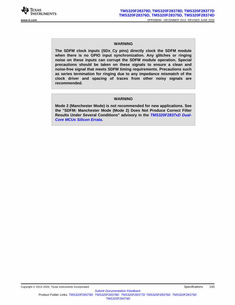
143
TMS320F28379D, TMS320F28378D, TMS320F28377DTMS320F28376D, TMS320F28375D, TMS320F28374D
www.ti.com SPRS880M –DECEMBER 2013–REVISED JUNE 2020
Submit Documentation FeedbackProduct Folder Links: TMS320F28379D TMS320F28378D TMS320F28377D TMS320F28376D TMS320F28375D
TMS320F28374D
SpecificationsCopyright © 2013–2020, Texas Instruments Incorporated
WARNING
The SDFM clock inputs (SDx_Cy pins) directly clock the SDFM modulewhen there is no GPIO input synchronization. Any glitches or ringingnoise on these inputs can corrupt the SDFM module operation. Specialprecautions should be taken on these signals to ensure a clean andnoise-free signal that meets SDFM timing requirements. Precautions suchas series termination for ringing due to any impedance mismatch of theclock driver and spacing of traces from other noisy signals arerecommended.
WARNING
Mode 2 (Manchester Mode) is not recommended for new applications. Seethe "SDFM: Manchester Mode (Mode 2) Does Not Produce Correct FilterResults Under Several Conditions" advisory in the TMS320F2837xD Dual-Core MCUs Silicon Errata.
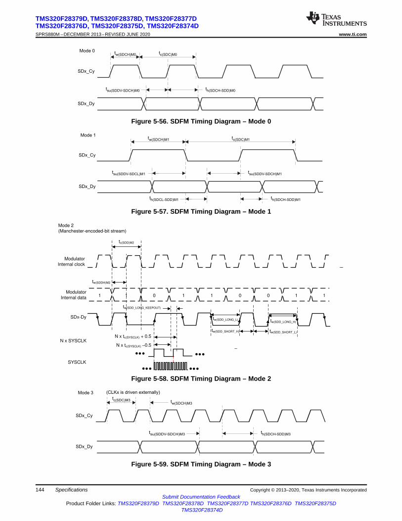
Mode 3
SDx_Cy
SDx_Dy
(CLKx is driven externally)
tc(SDC)M3 tw(SDCH)M3
tsu(SDDV-SDCH)M3 th(SDCH-SDD)M3
Modulator
Internal data
tc(SDD)M2
tw(SDDH)M2
Modulator
Internal clock
tw(SDD_LONG_KEEPOUT)
SDx-Dy
N x tc(SYSCLK) + 0.5
N x tc(SYSCLK) ±0.5
tw(SDD_LONG_L)
tw(SDD_SHORT_H) tw(SDD_SHORT_L)
tw(SDD_LONG_H)
N x SYSCLK
SYSCLK
Mode 2
(Manchester-encoded-bit stream)
1 1 0 1 01 0 1 1
±
tw(SDCH)M1 tc(SDC)M1
th(SDCL-SDD)M1 th(SDCH-SDD)M1
tsu(SDDV-SDCL)M1 tsu(SDDV-SDCH)M1
SDx_Cy
SDx_Dy
Mode 1
Mode 0 tw(SDCH)M0 tc(SDC)M0
th(SDCH-SDD)M0tsu(SDDV-SDCH)M0
SDx_Cy
SDx_Dy
144
TMS320F28379D, TMS320F28378D, TMS320F28377DTMS320F28376D, TMS320F28375D, TMS320F28374DSPRS880M –DECEMBER 2013–REVISED JUNE 2020 www.ti.com
Submit Documentation FeedbackProduct Folder Links: TMS320F28379D TMS320F28378D TMS320F28377D TMS320F28376D TMS320F28375D
TMS320F28374D
Specifications Copyright © 2013–2020, Texas Instruments Incorporated
Figure 5-56. SDFM Timing Diagram – Mode 0
Figure 5-57. SDFM Timing Diagram – Mode 1
Figure 5-58. SDFM Timing Diagram – Mode 2
Figure 5-59. SDFM Timing Diagram – Mode 3
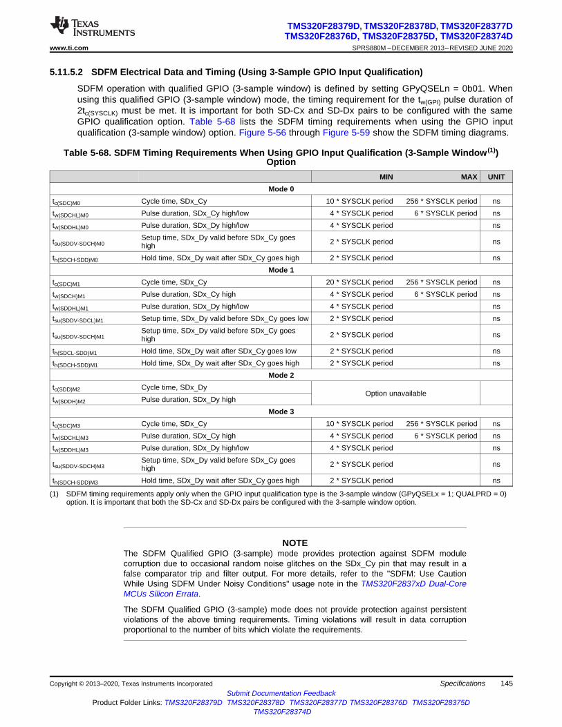
145
TMS320F28379D, TMS320F28378D, TMS320F28377DTMS320F28376D, TMS320F28375D, TMS320F28374D
www.ti.com SPRS880M –DECEMBER 2013–REVISED JUNE 2020
Submit Documentation FeedbackProduct Folder Links: TMS320F28379D TMS320F28378D TMS320F28377D TMS320F28376D TMS320F28375D
TMS320F28374D
SpecificationsCopyright © 2013–2020, Texas Instruments Incorporated
5.11.5.2 SDFM Electrical Data and Timing (Using 3-Sample GPIO Input Qualification)
SDFM operation with qualified GPIO (3-sample window) is defined by setting GPyQSELn = 0b01. Whenusing this qualified GPIO (3-sample window) mode, the timing requirement for the tw(GPI) pulse duration of2tc(SYSCLK) must be met. It is important for both SD-Cx and SD-Dx pairs to be configured with the sameGPIO qualification option. Table 5-68 lists the SDFM timing requirements when using the GPIO inputqualification (3-sample window) option. Figure 5-56 through Figure 5-59 show the SDFM timing diagrams.
(1) SDFM timing requirements apply only when the GPIO input qualification type is the 3-sample window (GPyQSELx = 1; QUALPRD = 0)option. It is important that both the SD-Cx and SD-Dx pairs be configured with the 3-sample window option.
Table 5-68. SDFM Timing Requirements When Using GPIO Input Qualification (3-Sample Window (1))Option
MIN MAX UNITMode 0
tc(SDC)M0 Cycle time, SDx_Cy 10 * SYSCLK period 256 * SYSCLK period nstw(SDCHL)M0 Pulse duration, SDx_Cy high/low 4 * SYSCLK period 6 * SYSCLK period nstw(SDDHL)M0 Pulse duration, SDx_Dy high/low 4 * SYSCLK period ns
tsu(SDDV-SDCH)M0Setup time, SDx_Dy valid before SDx_Cy goeshigh 2 * SYSCLK period ns
th(SDCH-SDD)M0 Hold time, SDx_Dy wait after SDx_Cy goes high 2 * SYSCLK period nsMode 1
tc(SDC)M1 Cycle time, SDx_Cy 20 * SYSCLK period 256 * SYSCLK period nstw(SDCH)M1 Pulse duration, SDx_Cy high 4 * SYSCLK period 6 * SYSCLK period nstw(SDDHL)M1 Pulse duration, SDx_Dy high/low 4 * SYSCLK period nstsu(SDDV-SDCL)M1 Setup time, SDx_Dy valid before SDx_Cy goes low 2 * SYSCLK period ns
tsu(SDDV-SDCH)M1Setup time, SDx_Dy valid before SDx_Cy goeshigh 2 * SYSCLK period ns
th(SDCL-SDD)M1 Hold time, SDx_Dy wait after SDx_Cy goes low 2 * SYSCLK period nsth(SDCH-SDD)M1 Hold time, SDx_Dy wait after SDx_Cy goes high 2 * SYSCLK period ns
Mode 2tc(SDD)M2 Cycle time, SDx_Dy
Option unavailabletw(SDDH)M2 Pulse duration, SDx_Dy high
Mode 3tc(SDC)M3 Cycle time, SDx_Cy 10 * SYSCLK period 256 * SYSCLK period nstw(SDCHL)M3 Pulse duration, SDx_Cy high 4 * SYSCLK period 6 * SYSCLK period nstw(SDDHL)M3 Pulse duration, SDx_Dy high/low 4 * SYSCLK period ns
tsu(SDDV-SDCH)M3Setup time, SDx_Dy valid before SDx_Cy goeshigh 2 * SYSCLK period ns
th(SDCH-SDD)M3 Hold time, SDx_Dy wait after SDx_Cy goes high 2 * SYSCLK period ns
NOTEThe SDFM Qualified GPIO (3-sample) mode provides protection against SDFM modulecorruption due to occasional random noise glitches on the SDx_Cy pin that may result in afalse comparator trip and filter output. For more details, refer to the "SDFM: Use CautionWhile Using SDFM Under Noisy Conditions" usage note in the TMS320F2837xD Dual-CoreMCUs Silicon Errata.
The SDFM Qualified GPIO (3-sample) mode does not provide protection against persistentviolations of the above timing requirements. Timing violations will result in data corruptionproportional to the number of bits which violate the requirements.
146
TMS320F28379D, TMS320F28378D, TMS320F28377DTMS320F28376D, TMS320F28375D, TMS320F28374DSPRS880M –DECEMBER 2013–REVISED JUNE 2020 www.ti.com
Submit Documentation FeedbackProduct Folder Links: TMS320F28379D TMS320F28378D TMS320F28377D TMS320F28376D TMS320F28375D
TMS320F28374D
Specifications Copyright © 2013–2020, Texas Instruments Incorporated
5.12 Communications Peripherals
NOTEFor the actual number of each peripheral on a specific device, see Table 3-1.
5.12.1 Controller Area Network (CAN)The CAN module performs CAN protocol communication according to ISO 11898-1 (identical to Bosch®
CAN protocol specification 2.0 A, B). The bit rate can be programmed to values up to 1 Mbps. A CANtransceiver chip is required for the connection to the physical layer (CAN bus).
For communication on a CAN network, individual message objects can be configured. The messageobjects and identifier masks are stored in the Message RAM.
All functions concerning the handling of messages are implemented in the message handler. Thesefunctions are: acceptance filtering; the transfer of messages between the CAN Core and the MessageRAM; and the handling of transmission requests.
The register set of the CAN may be accessed directly by the CPU through the module interface. Theseregisters are used to control and configure the CAN core and the message handler, and to access themessage RAM.
The CAN module implements the following features:• Complies with ISO11898-1 (Bosch® CAN protocol specification 2.0 A and B)• Bit rates up to 1 Mbps• Multiple clock sources• 32 message objects (“message objects” are also referred to as “mailboxes” in this document; the two
terms are used interchangeably), each with the following properties:– Configurable as receive or transmit– Configurable with standard (11-bit) or extended (29-bit) identifier– Supports programmable identifier receive mask– Supports data and remote frames– Holds 0 to 8 bytes of data– Parity-checked configuration and data RAM
• Individual identifier mask for each message object• Programmable FIFO mode for message objects• Programmable loop-back modes for self-test operation• Suspend mode for debug support• Software module reset• Automatic bus-on, after bus-off state by a programmable 32-bit timer• Message-RAM parity-check mechanism• Two interrupt lines
NOTEFor a CAN bit clock of 200 MHz, the smallest bit rate possible is 7.8125 kbps.
NOTEDepending on the timing settings used, the accuracy of the on-chip zero-pin oscillator(specified in the data manual) may not meet the requirements of the CAN protocol. In thissituation, an external clock source must be used.

CAN Core
Message
RAM
Interface
Message Handler
Register and Message
Object Access (IFx)
Module Interface
Message RAM
32
Message
Objects
(Mailboxes)
CAN
Test Modes
Only
3.3V CAN Transceiver
CANx RX pin CANx TX pin
CAN_H
CAN_LCAN Bus
CANINT0 CANINT1CPU Bus
External connections
Device
(to ePIE)
147
TMS320F28379D, TMS320F28378D, TMS320F28377DTMS320F28376D, TMS320F28375D, TMS320F28374D
www.ti.com SPRS880M –DECEMBER 2013–REVISED JUNE 2020
Submit Documentation FeedbackProduct Folder Links: TMS320F28379D TMS320F28378D TMS320F28377D TMS320F28376D TMS320F28375D
TMS320F28374D
SpecificationsCopyright © 2013–2020, Texas Instruments Incorporated
Figure 5-60 shows the CAN block diagram.
Figure 5-60. CAN Block Diagram
148
TMS320F28379D, TMS320F28378D, TMS320F28377DTMS320F28376D, TMS320F28375D, TMS320F28374DSPRS880M –DECEMBER 2013–REVISED JUNE 2020 www.ti.com
Submit Documentation FeedbackProduct Folder Links: TMS320F28379D TMS320F28378D TMS320F28377D TMS320F28376D TMS320F28375D
TMS320F28374D
Specifications Copyright © 2013–2020, Texas Instruments Incorporated
5.12.2 Inter-Integrated Circuit (I2C)The I2C module has the following features:• Compliance with the Philips Semiconductors I2C-bus specification (version 2.1):
– Support for 1-bit to 8-bit format transfers– 7-bit and 10-bit addressing modes– General call– START byte mode– Support for multiple master-transmitters and slave-receivers– Support for multiple slave-transmitters and master-receivers– Combined master transmit/receive and receive/transmit mode– Data transfer rate of from 10 kbps up to 400 kbps (I2C Fast-mode rate)
• One 16-byte receive FIFO and one 16-byte transmit FIFO• One interrupt that can be used by the CPU. This interrupt can be generated as a result of one of the
following conditions:– Transmit-data ready– Receive-data ready– Register-access ready– No-acknowledgment received– Arbitration lost– Stop condition detected– Addressed as slave
• An additional interrupt that can be used by the CPU when in FIFO mode• Module enable/disable capability• Free data format mode

I2CXSR I2CDXR
I2CRSR I2CDRR
ClockSynchronizer
Prescaler
Noise Filters
Arbitrator
I2C INT
Peripheral Bus
Interrupt toCPU/PIE
SDA
SCL
Control/StatusRegisters CPU
I C Module2
TX FIFO
RX FIFO
FIFO Interrupt toCPU/PIE
149
TMS320F28379D, TMS320F28378D, TMS320F28377DTMS320F28376D, TMS320F28375D, TMS320F28374D
www.ti.com SPRS880M –DECEMBER 2013–REVISED JUNE 2020
Submit Documentation FeedbackProduct Folder Links: TMS320F28379D TMS320F28378D TMS320F28377D TMS320F28376D TMS320F28375D
TMS320F28374D
SpecificationsCopyright © 2013–2020, Texas Instruments Incorporated
Figure 5-61 shows how the I2C peripheral module interfaces within the device.
Figure 5-61. I2C Peripheral Module Interfaces
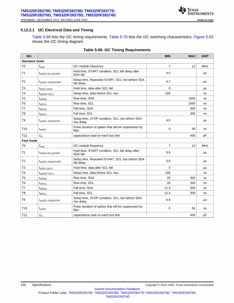
150
TMS320F28379D, TMS320F28378D, TMS320F28377DTMS320F28376D, TMS320F28375D, TMS320F28374DSPRS880M –DECEMBER 2013–REVISED JUNE 2020 www.ti.com
Submit Documentation FeedbackProduct Folder Links: TMS320F28379D TMS320F28378D TMS320F28377D TMS320F28376D TMS320F28375D
TMS320F28374D
Specifications Copyright © 2013–2020, Texas Instruments Incorporated
5.12.2.1 I2C Electrical Data and Timing
Table 5-69 lists the I2C timing requirements. Table 5-70 lists the I2C switching characteristics. Figure 5-62shows the I2C timing diagram.
Table 5-69. I2C Timing RequirementsNO. MIN MAX UNIT
Standard modeT0 fmod I2C module frequency 7 12 MHz
T1 th(SDA-SCL)STARTHold time, START condition, SCL fall delay afterSDA fall 4.0 µs
T2 tsu(SCL-SDA)STARTSetup time, Repeated START, SCL rise before SDAfall delay 4.7 µs
T3 th(SCL-DAT) Hold time, data after SCL fall 0 µsT4 tsu(DAT-SCL) Setup time, data before SCL rise 250 nsT5 tr(SDA) Rise time, SDA 1000 nsT6 tr(SCL) Rise time, SCL 1000 nsT7 tf(SDA) Fall time, SDA 300 nsT8 tf(SCL) Fall time, SCL 300 ns
T9 tsu(SCL-SDA)STOPSetup time, STOP condition, SCL rise before SDArise delay 4.0 µs
T10 tw(SP)Pulse duration of spikes that will be suppressed byfilter 0 50 ns
T11 Cb capacitance load on each bus line 400 pFFast modeT0 fmod I2C module frequency 7 12 MHz
T1 th(SDA-SCL)STARTHold time, START condition, SCL fall delay afterSDA fall 0.6 µs
T2 tsu(SCL-SDA)STARTSetup time, Repeated START, SCL rise before SDAfall delay 0.6 µs
T3 th(SCL-DAT) Hold time, data after SCL fall 0 µsT4 tsu(DAT-SCL) Setup time, data before SCL rise 100 nsT5 tr(SDA) Rise time, SDA 20 300 nsT6 tr(SCL) Rise time, SCL 20 300 nsT7 tf(SDA) Fall time, SDA 11.4 300 nsT8 tf(SCL) Fall time, SCL 11.4 300 ns
T9 tsu(SCL-SDA)STOPSetup time, STOP condition, SCL rise before SDArise delay 0.6 µs
T10 tw(SP)Pulse duration of spikes that will be suppressed byfilter 0 50 ns
T11 Cb capacitance load on each bus line 400 pF

S5
T6 T8
T5 T7 S3
S4
S2
STARTSTOP
SDA
SCL
SDA
SCL
T10S6
9th
clock
S7
Contd...
Contd...
T2
T1
Repeated
START
9th
clock
T9
STOP
ACK
ACK
151
TMS320F28379D, TMS320F28378D, TMS320F28377DTMS320F28376D, TMS320F28375D, TMS320F28374D
www.ti.com SPRS880M –DECEMBER 2013–REVISED JUNE 2020
Submit Documentation FeedbackProduct Folder Links: TMS320F28379D TMS320F28378D TMS320F28377D TMS320F28376D TMS320F28375D
TMS320F28374D
SpecificationsCopyright © 2013–2020, Texas Instruments Incorporated
Table 5-70. I2C Switching Characteristicsover recommended operating conditions (unless otherwise noted)
NO. PARAMETER TEST CONDITIONS MIN MAX UNITStandard modeS1 fSCL SCL clock frequency 0 100 kHzS2 TSCL SCL clock period 10 µsS3 tw(SCLL) Pulse duration, SCL clock low 4.7 µsS4 tw(SCLH) Pulse duration, SCL clock high 4.0 µs
S5 tBUFBus free time between STOP andSTART conditions 4.7 µs
S6 tv(SCL-DAT) Valid time, data after SCL fall 3.45 µsS7 tv(SCL-ACK) Valid time, Acknowledge after SCL fall 3.45 µsS8 II Input current on pins 0.1 Vbus < Vi < 0.9 Vbus –10 10 µAFast modeS1 fSCL SCL clock frequency 0 400 kHzS2 TSCL SCL clock period 2.5 µsS3 tw(SCLL) Pulse duration, SCL clock low 1.3 µsS4 tw(SCLH) Pulse duration, SCL clock high 0.6 µs
S5 tBUFBus free time between STOP andSTART conditions 1.3 µs
S6 tv(SCL-DAT) Valid time, data after SCL fall 0.9 µsS7 tv(SCL-ACK) Valid time, Acknowledge after SCL fall 0.9 µsS8 II Input current on pins 0.1 Vbus < Vi < 0.9 Vbus –10 10 µA
NOTETo meet all of the I2C protocol timing specifications, the I2C module clock (Fmod) must beconfigured from 7 MHz to 12 MHz.
Figure 5-62. I2C Timing Diagram
( )CLKSRG
CLKG =1+ CLKGDV
152
TMS320F28379D, TMS320F28378D, TMS320F28377DTMS320F28376D, TMS320F28375D, TMS320F28374DSPRS880M –DECEMBER 2013–REVISED JUNE 2020 www.ti.com
Submit Documentation FeedbackProduct Folder Links: TMS320F28379D TMS320F28378D TMS320F28377D TMS320F28376D TMS320F28375D
TMS320F28374D
Specifications Copyright © 2013–2020, Texas Instruments Incorporated
5.12.3 Multichannel Buffered Serial Port (McBSP)The McBSP module has the following features:• Compatible with McBSP in TMS320C28x and TMS320F28x DSP devices• Full-duplex communication• Double-buffered data registers that allow a continuous data stream• Independent framing and clocking for receive and transmit• External shift clock generation or an internal programmable frequency shift clock• 8-bit data transfer mode can be configured to transmit with LSB or MSB first• Programmable polarity for both frame synchronization and data clocks• Highly programmable internal clock and frame generation• Direct interface to industry-standard CODECs, Analog Interface Chips (AICs), and other serially
connected A/D and D/A devices• Supports AC97, I2S, and SPI protocols• McBSP clock rate,
where CLKSRG source could be LSPCLK, CLKX, or CLKR.

MDXx
MDRx
Expand Logic
DRR1 Receive Buffer
RXInterrupt
RBR1 RegisterRBR2 Register
MCLKXx
MFSXx
MCLKRx
MFSRx
16
Compand Logic
DXR2 Transmit Buffer
RSR1
XSR2 XSR1
Peripheral Read Bus
16
16
16
1616
RSR2
DXR1 Transmit BufferPERx.LSPCLK
MRINT
To CPU
RX Interrupt Logic
TXInterruptMXINT
To CPU TX Interrupt Logic
1616
16 16
Periphera
l B
us
DRR2 Receive Buffer
Peripheral Write Bus
Bridge
DMA BusCPU
CPU
CPU
McBSP TransmitInterrupt Select Logic
McBSP ReceiveInterrupt Select Logic
153
TMS320F28379D, TMS320F28378D, TMS320F28377DTMS320F28376D, TMS320F28375D, TMS320F28374D
www.ti.com SPRS880M –DECEMBER 2013–REVISED JUNE 2020
Submit Documentation FeedbackProduct Folder Links: TMS320F28379D TMS320F28378D TMS320F28377D TMS320F28376D TMS320F28375D
TMS320F28374D
SpecificationsCopyright © 2013–2020, Texas Instruments Incorporated
Figure 5-63 shows the block diagram of the McBSP module.
Figure 5-63. McBSP Block Diagram

154
TMS320F28379D, TMS320F28378D, TMS320F28377DTMS320F28376D, TMS320F28375D, TMS320F28374DSPRS880M –DECEMBER 2013–REVISED JUNE 2020 www.ti.com
Submit Documentation FeedbackProduct Folder Links: TMS320F28379D TMS320F28378D TMS320F28377D TMS320F28376D TMS320F28375D
TMS320F28374D
Specifications Copyright © 2013–2020, Texas Instruments Incorporated
5.12.3.1 McBSP Electrical Data and Timing
5.12.3.1.1 McBSP Transmit and Receive Timing
Table 5-71 shows the McBSP timing requirements. Table 5-72 shows the McBSP switchingcharacteristics. Figure 5-64 and Figure 5-65 show the McBSP timing diagrams.
(1) Polarity bits CLKRP = CLKXP = FSRP = FSXP = 0. If the polarity of any of the signals is inverted, then the timing references of thatsignal are also inverted.
(2) 2P = 1/CLKG in ns. CLKG is the output of sample rate generator mux. CLKG = CLKSRG / (1 + CLKGDV). CLKSRG can be LSPCLK,CLKX, CLKR as source. CLKSRG ≤ (SYSCLK/2).
Table 5-71. McBSP Timing Requirements (1) (2)
NO. MIN MAX UNIT
McBSP module clock (CLKG, CLKX, CLKR) range1 kHz
25 MHz
McBSP module cycle time (CLKG, CLKX, CLKR) range40 ns
1 msM11 tc(CKRX) Cycle time, CLKR/X CLKR/X ext 2P nsM12 tw(CKRX) Pulse duration, CLKR/X high or CLKR/X low CLKR/X ext P – 7 nsM13 tr(CKRX) Rise time, CLKR/X CLKR/X ext 7 nsM14 tf(CKRX) Fall time, CLKR/X CLKR/X ext 7 ns
M15 tsu(FRH-CKRL) Setup time, external FSR high before CLKR lowCLKR int 18
nsCLKR ext 2
M16 th(CKRL-FRH) Hold time, external FSR high after CLKR lowCLKR int 0
nsCLKR ext 6
M17 tsu(DRV-CKRL) Setup time, DR valid before CLKR lowCLKR int 18
nsCLKR ext 5
M18 th(CKRL-DRV) Hold time, DR valid after CLKR lowCLKR int 0
nsCLKR ext 3
M19 tsu(FXH-CKXL) Setup time, external FSX high before CLKX lowCLKX int 18
nsCLKX ext 2
M20 th(CKXL-FXH) Hold time, external FSX high after CLKX lowCLKX int 0
nsCLKX ext 6
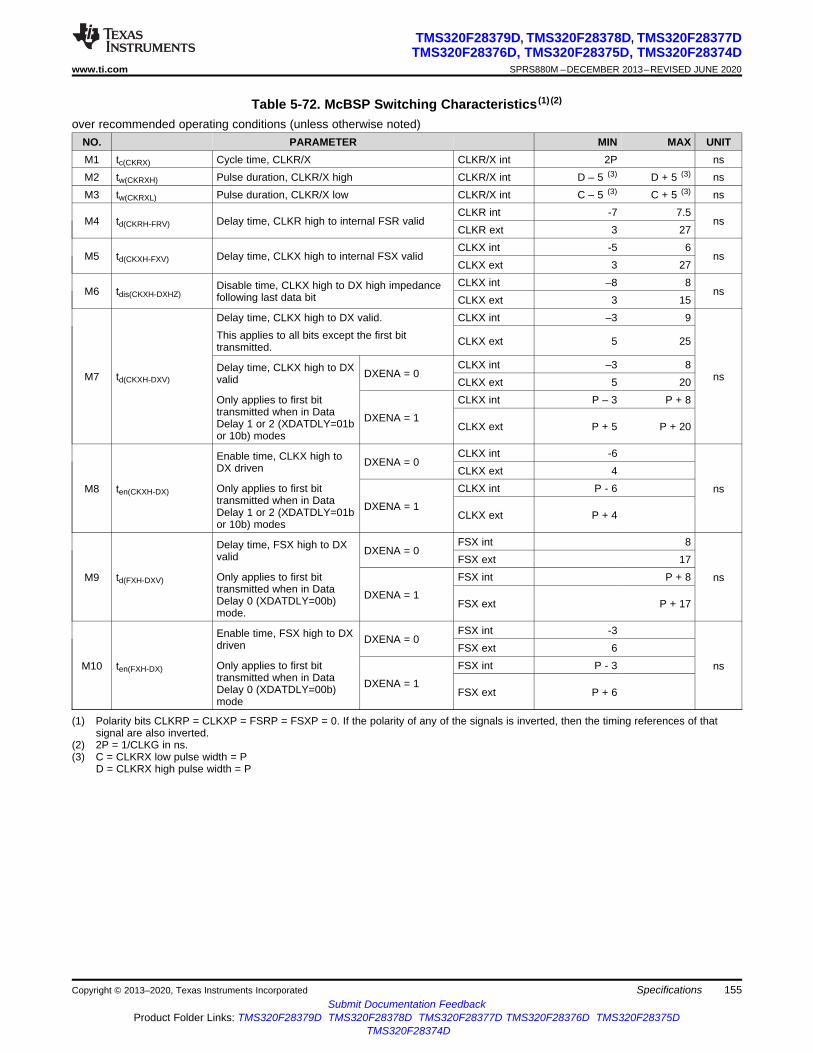
155
TMS320F28379D, TMS320F28378D, TMS320F28377DTMS320F28376D, TMS320F28375D, TMS320F28374D
www.ti.com SPRS880M –DECEMBER 2013–REVISED JUNE 2020
Submit Documentation FeedbackProduct Folder Links: TMS320F28379D TMS320F28378D TMS320F28377D TMS320F28376D TMS320F28375D
TMS320F28374D
SpecificationsCopyright © 2013–2020, Texas Instruments Incorporated
(1) Polarity bits CLKRP = CLKXP = FSRP = FSXP = 0. If the polarity of any of the signals is inverted, then the timing references of thatsignal are also inverted.
(2) 2P = 1/CLKG in ns.(3) C = CLKRX low pulse width = P
D = CLKRX high pulse width = P
Table 5-72. McBSP Switching Characteristics (1) (2)
over recommended operating conditions (unless otherwise noted)NO. PARAMETER MIN MAX UNITM1 tc(CKRX) Cycle time, CLKR/X CLKR/X int 2P nsM2 tw(CKRXH) Pulse duration, CLKR/X high CLKR/X int D – 5 (3) D + 5 (3) nsM3 tw(CKRXL) Pulse duration, CLKR/X low CLKR/X int C – 5 (3) C + 5 (3) ns
M4 td(CKRH-FRV) Delay time, CLKR high to internal FSR validCLKR int -7 7.5
nsCLKR ext 3 27
M5 td(CKXH-FXV) Delay time, CLKX high to internal FSX validCLKX int -5 6
nsCLKX ext 3 27
M6 tdis(CKXH-DXHZ)Disable time, CLKX high to DX high impedancefollowing last data bit
CLKX int –8 8ns
CLKX ext 3 15
M7 td(CKXH-DXV)
Delay time, CLKX high to DX valid. CLKX int –3 9
ns
This applies to all bits except the first bittransmitted. CLKX ext 5 25
Delay time, CLKX high to DXvalid DXENA = 0
CLKX int –3 8CLKX ext 5 20
Only applies to first bittransmitted when in DataDelay 1 or 2 (XDATDLY=01bor 10b) modes
DXENA = 1
CLKX int P – 3 P + 8
CLKX ext P + 5 P + 20
M8 ten(CKXH-DX)
Enable time, CLKX high toDX driven DXENA = 0
CLKX int -6
ns
CLKX ext 4Only applies to first bittransmitted when in DataDelay 1 or 2 (XDATDLY=01bor 10b) modes
DXENA = 1
CLKX int P - 6
CLKX ext P + 4
M9 td(FXH-DXV)
Delay time, FSX high to DXvalid DXENA = 0
FSX int 8
ns
FSX ext 17Only applies to first bittransmitted when in DataDelay 0 (XDATDLY=00b)mode.
DXENA = 1
FSX int P + 8
FSX ext P + 17
M10 ten(FXH-DX)
Enable time, FSX high to DXdriven DXENA = 0
FSX int -3
ns
FSX ext 6Only applies to first bittransmitted when in DataDelay 0 (XDATDLY=00b)mode
DXENA = 1
FSX int P - 3
FSX ext P + 6
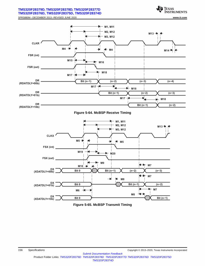
M8
M7
M7M8
M6
M7M9
M10
(XDATDLY=10b)DX
(XDATDLY=01b)DX
(XDATDLY=00b)DX
Bit (n−1)Bit 0
Bit (n−1) (n−3)(n−2)Bit 0
(n−2)Bit (n−1)Bit 0
M20
M13M3, M12
M1, M11
M2, M12
FSX (ext)
FSX (int)
CLKX
M5M5
M19
(n−2)Bit (n−1)
(n−3)(n−2)Bit (n−1)
(n−4)(n−3)(n−2)Bit (n−1)
M18M17
M18M17
M17M18
M16M15
M4M4M14
M13M3, M12
M1, M11
M2, M12
(RDATDLY=10b)DR
(RDATDLY=01b)DR
(RDATDLY=00b)DR
FSR (ext)
FSR (int)
CLKR
156
TMS320F28379D, TMS320F28378D, TMS320F28377DTMS320F28376D, TMS320F28375D, TMS320F28374DSPRS880M –DECEMBER 2013–REVISED JUNE 2020 www.ti.com
Submit Documentation FeedbackProduct Folder Links: TMS320F28379D TMS320F28378D TMS320F28377D TMS320F28376D TMS320F28375D
TMS320F28374D
Specifications Copyright © 2013–2020, Texas Instruments Incorporated
Figure 5-64. McBSP Receive Timing
Figure 5-65. McBSP Transmit Timing
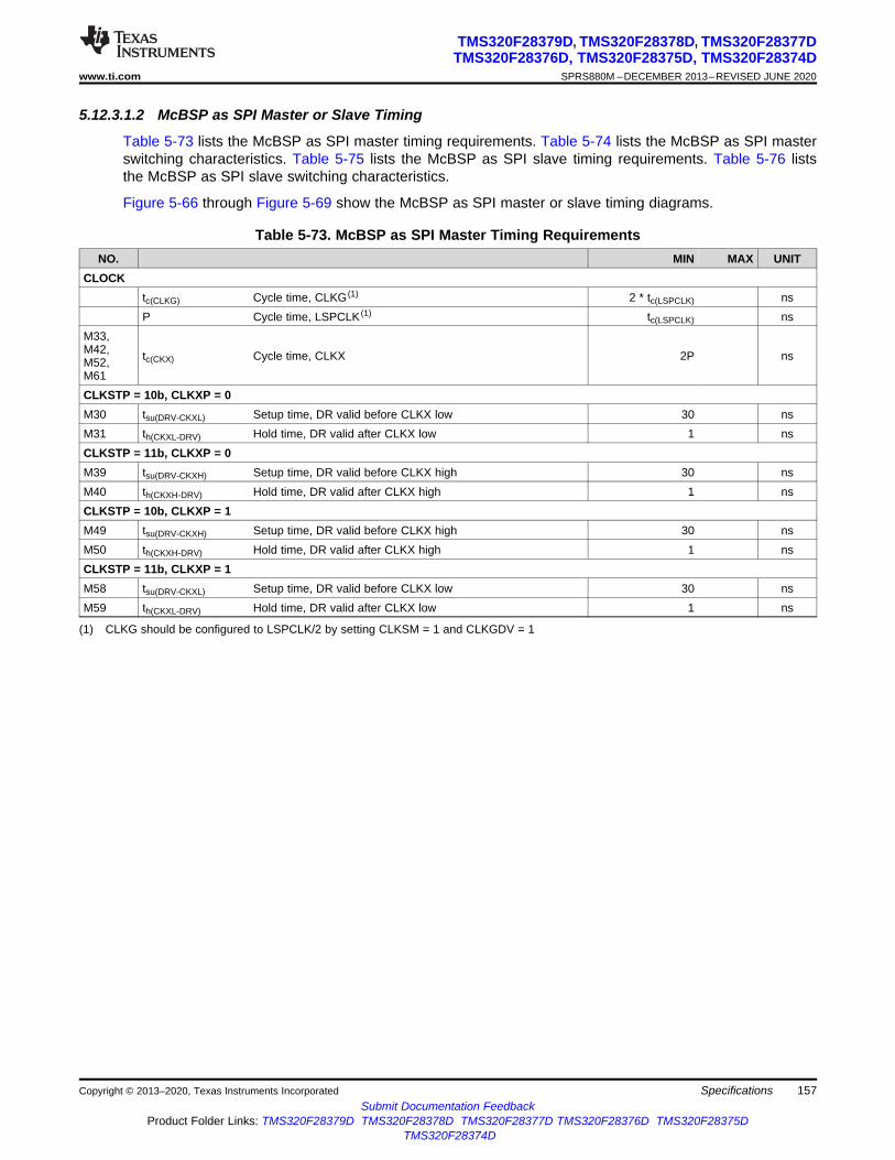
157
TMS320F28379D, TMS320F28378D, TMS320F28377DTMS320F28376D, TMS320F28375D, TMS320F28374D
www.ti.com SPRS880M –DECEMBER 2013–REVISED JUNE 2020
Submit Documentation FeedbackProduct Folder Links: TMS320F28379D TMS320F28378D TMS320F28377D TMS320F28376D TMS320F28375D
TMS320F28374D
SpecificationsCopyright © 2013–2020, Texas Instruments Incorporated
5.12.3.1.2 McBSP as SPI Master or Slave Timing
Table 5-73 lists the McBSP as SPI master timing requirements. Table 5-74 lists the McBSP as SPI masterswitching characteristics. Table 5-75 lists the McBSP as SPI slave timing requirements. Table 5-76 liststhe McBSP as SPI slave switching characteristics.
Figure 5-66 through Figure 5-69 show the McBSP as SPI master or slave timing diagrams.
(1) CLKG should be configured to LSPCLK/2 by setting CLKSM = 1 and CLKGDV = 1
Table 5-73. McBSP as SPI Master Timing RequirementsNO. MIN MAX UNIT
CLOCKtc(CLKG) Cycle time, CLKG (1) 2 * tc(LSPCLK) nsP Cycle time, LSPCLK (1) tc(LSPCLK) ns
M33,M42,M52,M61
tc(CKX) Cycle time, CLKX 2P ns
CLKSTP = 10b, CLKXP = 0M30 tsu(DRV-CKXL) Setup time, DR valid before CLKX low 30 nsM31 th(CKXL-DRV) Hold time, DR valid after CLKX low 1 nsCLKSTP = 11b, CLKXP = 0M39 tsu(DRV-CKXH) Setup time, DR valid before CLKX high 30 nsM40 th(CKXH-DRV) Hold time, DR valid after CLKX high 1 nsCLKSTP = 10b, CLKXP = 1M49 tsu(DRV-CKXH) Setup time, DR valid before CLKX high 30 nsM50 th(CKXH-DRV) Hold time, DR valid after CLKX high 1 nsCLKSTP = 11b, CLKXP = 1M58 tsu(DRV-CKXL) Setup time, DR valid before CLKX low 30 nsM59 th(CKXL-DRV) Hold time, DR valid after CLKX low 1 ns
158
TMS320F28379D, TMS320F28378D, TMS320F28377DTMS320F28376D, TMS320F28375D, TMS320F28374DSPRS880M –DECEMBER 2013–REVISED JUNE 2020 www.ti.com
Submit Documentation FeedbackProduct Folder Links: TMS320F28379D TMS320F28378D TMS320F28377D TMS320F28376D TMS320F28375D
TMS320F28374D
Specifications Copyright © 2013–2020, Texas Instruments Incorporated
(1) CLKG should be configured to LSPCLK/2 by setting CLKSM = 1 and CLKGDV = 1.
Table 5-74. McBSP as SPI Master Switching Characteristicsover operating free-air temperature range (unless otherwise noted)
NO. PARAMETER MIN TYP MAX UNITCLOCKM33 tc(CLKG) Cycle time, CLKG (1) (n * tc(LSPCLK)) 40 ns
P Half CLKG cycle; 0.5 * tc(CLKG) 20 nsn LSPCLK to CLKG divider 2 ns
CLKSTP = 10b, CLKXP = 0M24 th(CKXL-FXL) Hold time, FSX high after CLKX low 2P – 6 nsM25 td(FXL-CKXH) Delay time, FSX low to CLKX high P – 6 ns
M26 td(CLKXH-DXV)Delay time, CLKX high to DX valid [check clock polarity andadd to timing diagram] –4 6 ns
M28 tdis(FXH-DXHZ)Disable time, DX high impedance following last data bit fromCLKX low [redefine timing diagram] P – 8 ns
M29 td(FXL-DXV) Delay time, FSX low to DX valid P – 3 P + 6 nsCLKSTP = 11b, CLKXP = 0M34 th(CKXL-FXH) Hold time, FSX high after CLKX low P – 6 nsM35 td(FXL-CKXH) Delay time, FSX low to CLKX high P – 6 ns
M36 td(CLKXL-DXV)Delay time, CLKX low to DX valid [check clock polarity andadd to timing diagram] –4 6 ns
M37 tdis(CKXL-DXHZ)Disable time, DX high impedance following last data bit fromCLKX low P – 6 ns
M38 td(FXL-DXV) Delay time, FSX low to DX valid –2 1 nsCLKSTP = 10b, CLKXP = 1M43 th(CKXH-FXH) Hold time, FSX high after CLKX high 2P – 6 nsM44 td(FXL-CKXL) Delay time, FSX low to CLKX low P – 6 ns
M45 td(CLKXL-DXV)Delay time, CLKX low to DX valid [check clock polarity andadd to timing diagram] –4 6 ns
M47 tdis(FXH-DXHZ)Disable time, DX high impedance following last data bit fromCLKX low [redefine timing diagram] P – 6 ns
M48 td(FXL-DXV) Delay time, FSX low to DX valid –2 1 nsCLKSTP = 11b, CLKXP = 1M53 th(CKXH-FXH) Hold time, FSX high after CLKX high P – 6 nsM54 td(FXL-CKXL) Delay time, FSX low to CLKX low 2P – 6 nsM55 td(CLKXH-DXV) Delay time, CLKX high to DX valid –4 6 ns
M56 tdis(CKXH-DXHZ)Disable time, DX high impedance following last data bit fromCLKX high P – 8 ns
M57 td(FXL-DXV) Delay time, FSX low to DX valid –2 1 ns

159
TMS320F28379D, TMS320F28378D, TMS320F28377DTMS320F28376D, TMS320F28375D, TMS320F28374D
www.ti.com SPRS880M –DECEMBER 2013–REVISED JUNE 2020
Submit Documentation FeedbackProduct Folder Links: TMS320F28379D TMS320F28378D TMS320F28377D TMS320F28376D TMS320F28375D
TMS320F28374D
SpecificationsCopyright © 2013–2020, Texas Instruments Incorporated
(1) CLKG should be configured to LSPCLK/2 by setting CLKSM = 1 and CLKGDV = 1(2) For SPI slave modes CLKX must be a minimum of 8 CLKG cycles
Table 5-75. McBSP as SPI Slave Timing RequirementsNO. MIN MAX UNIT
CLOCKtc(CLKG) Cycle time, CLKG (1) 2 * tc(LSPCLK) nsP Cycle time, LSPCLK (1) tc(LSPCLK) ns
M33,M42,M52,M61
tc(CKX) Cycle time, CLKX (2) 16P ns
na tskew(CKX-Data)Worst skew between Clock and Data to ensure GBD forsampled clock and datas ns
CLKSTP = 10b, CLKXP = 0M30 tsu(DRV-CKXL) Setup time, DR valid before CLKX low 8P – 10 nsM31 th(CKXL-DRV) Hold time, DR valid after CLKX low 8P – 10 nsM32 tsu(BFXL-CKXH) Setup time, FSX low before CLKX high 8P+10 nsCLKSTP = 11b, CLKXP = 0M39 tsu(DRV-CKXH) Setup time, DR valid before CLKX high 8P – 10 nsM40 th(CKXH-DRV) Hold time, DR valid after CLKX high 8P – 10 nsM41 tsu(FXL-CKXH) Setup time, FSX low before CLKX high 16P+10 nsCLKSTP = 10b, CLKXP = 1M49 tsu(DRV-CKXH) Setup time, DR valid before CLKX high 8P – 10 nsM50 th(CKXH-DRV) Hold time, DR valid after CLKX high 8P – 10 nsM51 tsu(FXL-CKXL) Setup time, FSX low before CLKX low 8P+10 nsCLKSTP = 11b, CLKXP = 1M58 tsu(DRV-CKXL) Setup time, DR valid before CLKX low 8P – 10 nsM59 th(CKXL-DRV) Hold time, DR valid after CLKX low 8P – 10 nsM60 tsu(FXL-CKXL) Setup time, FSX low before CLKX low 16P+10 ns

Bit 0 Bit(n-1) (n-2) (n-3) (n-4)
Bit 0 Bit(n-1) (n-2) (n-3) (n-4)
CLKX
FSX
DX
DR
M35
M37
M40M39
M38
M34
LSB MSBM41M42
M36
Bit 0 Bit(n-1) (n-2) (n-3) (n-4)
Bit 0 Bit(n-1) (n-2) (n-3) (n-4)
CLKX
FSX
DX
M30M31
DR
M24
M29
M25
LSB MSBM32 M33
M28 M26
160
TMS320F28379D, TMS320F28378D, TMS320F28377DTMS320F28376D, TMS320F28375D, TMS320F28374DSPRS880M –DECEMBER 2013–REVISED JUNE 2020 www.ti.com
Submit Documentation FeedbackProduct Folder Links: TMS320F28379D TMS320F28378D TMS320F28377D TMS320F28376D TMS320F28375D
TMS320F28374D
Specifications Copyright © 2013–2020, Texas Instruments Incorporated
Table 5-76. McBSP as SPI Slave Switching Characteristicsover operating free-air temperature range (unless otherwise noted)
NO. PARAMETER MIN TYP MAX UNITCLOCK
2P Cycle time, CLKG nsCLKSTP = 10b, CLKXP = 0M26 td(CLKXH-DXV) Delay time, CLKX high to DX valid 3P + 6 5P + 20 ns
M28 tdis(FXH-DXHZ)Disable time, DX high impedance following last data bit fromFSX high 6P + 6 ns
M29 td(FXL-DXV) Delay time, FSX low to DX valid 4P + 6 nsCLKSTP = 11b, CLKXP = 0M36 td(CLKXL-DXV) Delay time, CLKX low to DX valid 3P + 6 5P + 20 ns
M37 tdis(CKXL-DXHZ)Disable time, DX high impedance following last data bit fromCLKX low 7P + 6 ns
M38 td(FXL-DXV) Delay time, FSX low to DX valid 4P + 6 nsCLKSTP = 10b, CLKXP = 1M45 td(CLKXL-DXV) Delay time, CLKX low to DX valid 3P + 6 5P + 20 ns
M47 tdis(FXH-DXHZ)Disable time, DX high impedance following last data bit fromFSX high 6P + 6 ns
M48 td(FXL-DXV) Delay time, FSX low to DX valid 4P + 6 nsCLKSTP = 11b, CLKXP = 1M55 td(CLKXH-DXV) Delay time, CLKX high to DX valid 3P + 6 5P + 20 ns
M56 tdis(CKXH-DXHZ)Disable time, DX high impedance following last data bit fromCLKX high 7P + 6 ns
M57 td(FXL-DXV) Delay time, FSX low to DX valid 4P + 6 ns
Figure 5-66. McBSP Timing as SPI Master or Slave: CLKSTP = 10b, CLKXP = 0
Figure 5-67. McBSP Timing as SPI Master or Slave: CLKSTP = 11b, CLKXP = 0

Bit 0 Bit(n-1) (n-2) (n-3) (n-4)
Bit 0 Bit(n-1) (n-2) (n-3) (n-4)
CLKX
FSX
DX
DR
M54
M58
M56
M53
M55
M59
M57
LSB MSBM60 M61
M51
M50
Bit 0 Bit(n-1) (n-2) (n-3) (n-4)
Bit 0 Bit(n-1) (n-2) (n-3) (n-4)
CLKX
FSX
DX
DR
M44
M48
M49
M43
LSB MSB M52
M47 M45
161
TMS320F28379D, TMS320F28378D, TMS320F28377DTMS320F28376D, TMS320F28375D, TMS320F28374D
www.ti.com SPRS880M –DECEMBER 2013–REVISED JUNE 2020
Submit Documentation FeedbackProduct Folder Links: TMS320F28379D TMS320F28378D TMS320F28377D TMS320F28376D TMS320F28375D
TMS320F28374D
SpecificationsCopyright © 2013–2020, Texas Instruments Incorporated
Figure 5-68. McBSP Timing as SPI Master or Slave: CLKSTP = 10b, CLKXP = 1
Figure 5-69. McBSP Timing as SPI Master or Slave: CLKSTP = 11b, CLKXP = 1

162
TMS320F28379D, TMS320F28378D, TMS320F28377DTMS320F28376D, TMS320F28375D, TMS320F28374DSPRS880M –DECEMBER 2013–REVISED JUNE 2020 www.ti.com
Submit Documentation FeedbackProduct Folder Links: TMS320F28379D TMS320F28378D TMS320F28377D TMS320F28376D TMS320F28375D
TMS320F28374D
Specifications Copyright © 2013–2020, Texas Instruments Incorporated
5.12.4 Serial Communications Interface (SCI)The SCI is a 2-wire asynchronous serial port, commonly known as a UART. The SCI module supportsdigital communications between the CPU and other asynchronous peripherals that use the standard non-return-to-zero (NRZ) format
The SCI receiver and transmitter each have a 16-level-deep FIFO for reducing servicing overhead, andeach has its own separate enable and interrupt bits. Both can be operated independently for half-duplexcommunication, or simultaneously for full-duplex communication. To specify data integrity, the SCI checksreceived data for break detection, parity, overrun, and framing errors. The bit rate is programmable todifferent speeds through a 16-bit baud-select register. Figure 5-70 shows the SCI block diagram.
Features of the SCI module include:• Two external pins:
– SCITXD: SCI transmit-output pin– SCIRXD: SCI receive-input pin
NOTE: Both pins can be used as GPIO if not used for SCI.– Baud rate programmable to 64K different rates
• Data-word format– One start bit– Data-word length programmable from 1 to 8 bits– Optional even/odd/no parity bit– 1 or 2 stop bits
• Four error-detection flags: parity, overrun, framing, and break detection• Two wakeup multiprocessor modes: idle-line and address bit• Half- or full-duplex operation• Double-buffered receive and transmit functions• Transmitter and receiver operations can be accomplished through interrupt-driven or polled algorithms
with status flags.– Transmitter: TXRDY flag (transmitter-buffer register is ready to receive another character) and TX
EMPTY flag (transmitter-shift register is empty)– Receiver: RXRDY flag (receiver-buffer register is ready to receive another character), BRKDT flag
(break condition occurred), and RX ERROR flag (monitoring four interrupt conditions)• Separate enable bits for transmitter and receiver interrupts (except BRKDT)• NRZ format• Auto baud-detect hardware logic• 16-level transmit and receive FIFO
NOTEAll registers in this module are 8-bit registers. When a register is accessed, the register datais in the lower byte (bits 7–0), and the upper byte (bits 15–8) is read as zeros. Writing to theupper byte has no effect.
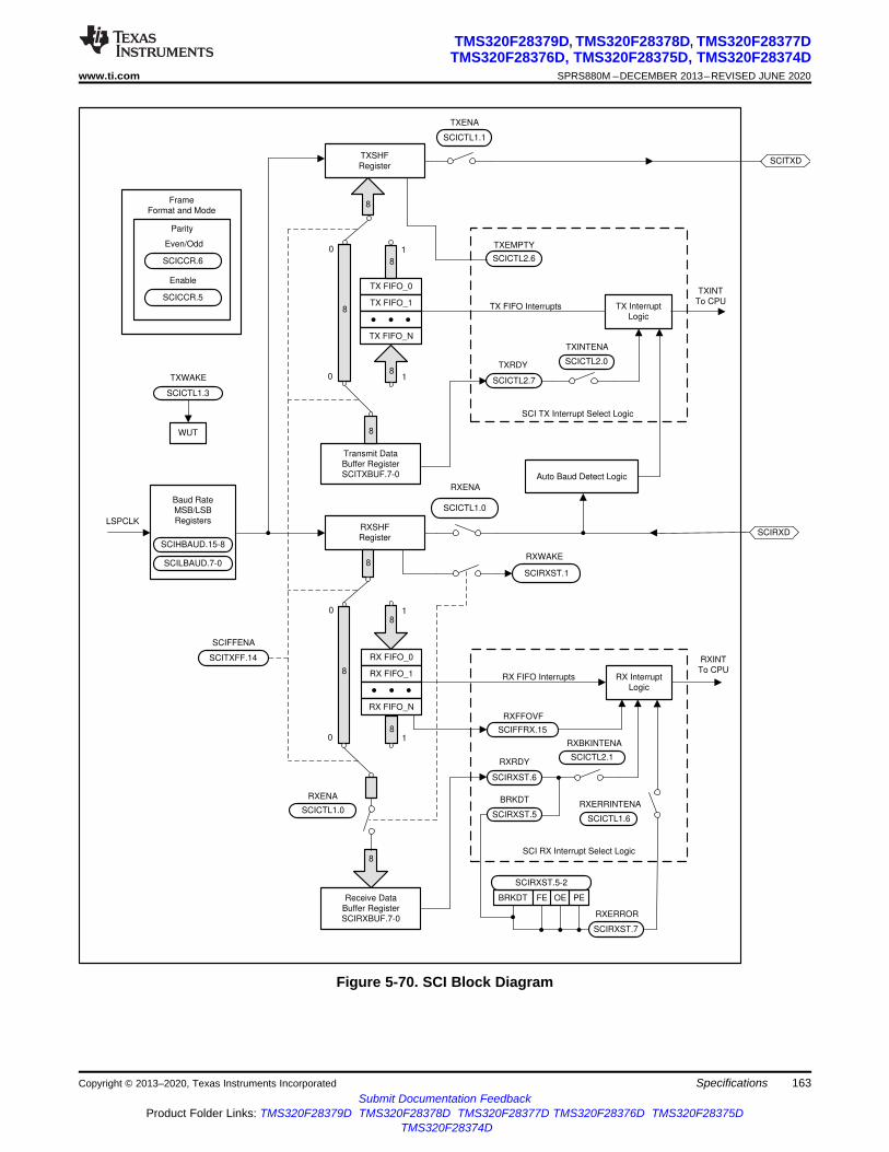
TXSHF
Register
TX FIFO_0
TX FIFO_1
TX FIFO_N
8
8
Transmit Data
Buffer Register
SCITXBUF.7-0
RXSHF
Register
RX FIFO_0
RX FIFO_1
RX FIFO_N
8
Receive Data
Buffer Register
SCIRXBUF.7-0
RXENA
SCICTL1.0
8
TX FIFO Interrupts
RX FIFO Interrupts
Baud Rate
MSB/LSB
Registers
SCIHBAUD.15-8
SCILBAUD.7-0
LSPCLK
Frame
Format and Mode
Parity
SCICCR.6
SCICCR.5
Even/Odd
Enable
SCICTL1.3
TXWAKE
WUT
SCICTL1.1
TXENA
RXENA
SCICTL2.6
TXEMPTY
RXFFOVF
SCICTL2.7
TXRDY SCICTL2.0
TXINTENA
SCIRXST.6
RXRDY
SCIRXST.5
BRKDT
SCICTL2.1
RXBKINTENA
TX Interrupt
Logic
RX Interrupt
Logic
SCIRXST.7
RXERROR
SCICTL1.6
RXERRINTENA
SCI RX Interrupt Select Logic
8
8
8
8
8
8
0 1
0 1
0 1
0 1
SCIFFENA
SCITXFF.14
RXWAKE
SCIRXST.1
Auto Baud Detect Logic
TXINT
To CPU
RXINT
To CPU
SCITXD
SCIRXD
BRKDT FE OE PE
SCIRXST.5-2
8
SCICTL1.0
SCIFFRX.15
SCI TX Interrupt Select Logic
163
TMS320F28379D, TMS320F28378D, TMS320F28377DTMS320F28376D, TMS320F28375D, TMS320F28374D
www.ti.com SPRS880M –DECEMBER 2013–REVISED JUNE 2020
Submit Documentation FeedbackProduct Folder Links: TMS320F28379D TMS320F28378D TMS320F28377D TMS320F28376D TMS320F28375D
TMS320F28374D
SpecificationsCopyright © 2013–2020, Texas Instruments Incorporated
Figure 5-70. SCI Block Diagram
164
TMS320F28379D, TMS320F28378D, TMS320F28377DTMS320F28376D, TMS320F28375D, TMS320F28374DSPRS880M –DECEMBER 2013–REVISED JUNE 2020 www.ti.com
Submit Documentation FeedbackProduct Folder Links: TMS320F28379D TMS320F28378D TMS320F28377D TMS320F28376D TMS320F28375D
TMS320F28374D
Specifications Copyright © 2013–2020, Texas Instruments Incorporated
The major elements used in full-duplex operation include:• A transmitter (TX) and its major registers:
– SCITXBUF register – Transmitter Data Buffer register. Contains data (loaded by the CPU) to betransmitted
– TXSHF register – Transmitter Shift register. Accepts data from the SCITXBUF register and shiftsdata onto the SCITXD pin, 1 bit at a time
• A receiver (RX) and its major registers:– RXSHF register – Receiver Shift register. Shifts data in from the SCIRXD pin, 1 bit at a time– SCIRXBUF register – Receiver Data Buffer register. Contains data to be read by the CPU. Data
from a remote processor is loaded into the RXSHF register and then into the SCIRXBUF andSCIRXEMU registers
• A programmable baud generator• Data-memory-mapped control and status registers enable the CPU to access the I2C module registers
and FIFOs.
The SCI receiver and transmitter operate independently.
165
TMS320F28379D, TMS320F28378D, TMS320F28377DTMS320F28376D, TMS320F28375D, TMS320F28374D
www.ti.com SPRS880M –DECEMBER 2013–REVISED JUNE 2020
Submit Documentation FeedbackProduct Folder Links: TMS320F28379D TMS320F28378D TMS320F28377D TMS320F28376D TMS320F28375D
TMS320F28374D
SpecificationsCopyright © 2013–2020, Texas Instruments Incorporated
5.12.5 Serial Peripheral Interface (SPI)The SPI is a high-speed synchronous serial input/output (I/O) port that allows a serial bit stream ofprogrammed length (1 to 16 bits) to be shifted into and out of the device at a programmed bit-transfer rate.The SPI is normally used for communications between the microcontroller and external peripherals oranother controller. Typical applications include external I/O or peripheral expansion through devices suchas shift registers, display drivers, and ADCs. Multidevice communications are supported by themaster/slave operation of the SPI. The port supports 16-level receive and transmit FIFOs for reducingCPU servicing overhead.
The SPI module features include:• SPISOMI: SPI slave-output/master-input pin• SPISIMO: SPI slave-input/master-output pin• SPISTE: SPI slave transmit-enable pin• SPICLK: SPI serial-clock pin• Two operational modes: master and slave• Baud rate: 125 different programmable rates• Data word length: 1 to 16 data bits• Four clocking schemes (controlled by clock polarity and clock phase bits) include:
– Falling edge without phase delay: SPICLK active-high. SPI transmits data on the falling edge of theSPICLK signal and receives data on the rising edge of the SPICLK signal.
– Falling edge with phase delay: SPICLK active-high. SPI transmits data one half-cycle ahead of thefalling edge of the SPICLK signal and receives data on the falling edge of the SPICLK signal.
– Rising edge without phase delay: SPICLK inactive-low. SPI transmits data on the rising edge of theSPICLK signal and receives data on the falling edge of the SPICLK signal.
– Rising edge with phase delay: SPICLK inactive-low. SPI transmits data one half-cycle ahead of therising edge of the SPICLK signal and receives data on the rising edge of the SPICLK signal.
• Simultaneous receive-and-transmit operation (transmit function can be disabled in software)• Transmitter and receiver operations are accomplished through either interrupt-driven or polled
algorithms.• 16-level transmit and receive FIFO• Delayed transmit control• 3-wire SPI mode• SPISTE inversion for digital audio interface receive mode on devices with two SPI modules• DMA support• High-speed mode for up to 50-MHz full-duplex communication
SPISIMO
SPISOMI
SPICLK
SPISTE
SPI
Low-Speed
Prescaler
DMA
PIE
LSPCLK SYSCLK
SYSRS
SPIINT
SPITXINT
SPIRXDMA
SPITXDMA
Pe
rip
he
ral
Bu
s
CPU
PCLKCR8
GPIO
MUX
Bit
Clock
166
TMS320F28379D, TMS320F28378D, TMS320F28377DTMS320F28376D, TMS320F28375D, TMS320F28374DSPRS880M –DECEMBER 2013–REVISED JUNE 2020 www.ti.com
Submit Documentation FeedbackProduct Folder Links: TMS320F28379D TMS320F28378D TMS320F28377D TMS320F28376D TMS320F28375D
TMS320F28374D
Specifications Copyright © 2013–2020, Texas Instruments Incorporated
The SPI operates in master or slave mode. The master initiates data transfer by sending the SPICLKsignal. For both the slave and the master, data is shifted out of the shift registers on one edge of theSPICLK and latched into the shift register on the opposite SPICLK clock edge. If the CLOCK PHASE bit(SPICTL.3) is high, data is transmitted and received a half-cycle before the SPICLK transition. As a result,both controllers send and receive data simultaneously. The application software determines whether thedata is meaningful or dummy data. There are three possible methods for data transmission:• Master sends data; slave sends dummy data• Master sends data; slave sends data• Master sends dummy data; slave sends data
The master can initiate a data transfer at any time because it controls the SPICLK signal. The software,however, determines how the master detects when the slave is ready to broadcast data.
Figure 5-71 shows the SPI CPU Interface.
Figure 5-71. SPI CPU Interface
167
TMS320F28379D, TMS320F28378D, TMS320F28377DTMS320F28376D, TMS320F28375D, TMS320F28374D
www.ti.com SPRS880M –DECEMBER 2013–REVISED JUNE 2020
Submit Documentation FeedbackProduct Folder Links: TMS320F28379D TMS320F28378D TMS320F28377D TMS320F28376D TMS320F28375D
TMS320F28374D
SpecificationsCopyright © 2013–2020, Texas Instruments Incorporated
5.12.5.1 SPI Electrical Data and Timing
NOTEAll timing parameters for SPI High-Speed Mode assume a load capacitance of 5 pF onSPICLK, SPISIMO, and SPISOMI.
For more information about the SPI in High-Speed mode, see the Serial Peripheral Interface (SPI) chapterof the TMS320F2837xD Dual-Core Microcontrollers Technical Reference Manual.
To use the SPI in High-Speed mode, the application must use the high-speed enabled GPIOs (seeSection 4.4.5).
5.12.5.1.1 SPI Master Mode Timings
Table 5-77 lists the SPI master mode timing requirements. Table 5-78 lists the SPI master mode switchingcharacteristics (clock phase = 0). Table 5-79 lists the SPI master mode switching characteristics (clockphase = 1). Figure 5-72 shows the SPI master mode external timing where the clock phase = 0. Figure 5-73 shows the SPI master mode external timing where the clock phase = 1.
(1) The (BRR + 1) condition is Even when (SPIBRR + 1) is even or SPIBRR is 0 or 2. It is Odd when (SPIBRR + 1) is odd and SPIBRR isgreater than 3.
Table 5-77. SPI Master Mode Timing Requirements
NO. (BRR + 1)CONDITION (1) MIN MAX UNIT
High Speed Mode
8 tsu(SOMI)MSetup time, SPISOMI valid beforeSPICLK Even, Odd 1 ns
9 th(SOMI)MHold time, SPISOMI valid afterSPICLK Even, Odd 5 ns
Normal Mode
8 tsu(SOMI)MSetup time, SPISOMI valid beforeSPICLK Even, Odd 20 ns
9 th(SOMI)MHold time, SPISOMI valid afterSPICLK Even, Odd 0 ns

168
TMS320F28379D, TMS320F28378D, TMS320F28377DTMS320F28376D, TMS320F28375D, TMS320F28374DSPRS880M –DECEMBER 2013–REVISED JUNE 2020 www.ti.com
Submit Documentation FeedbackProduct Folder Links: TMS320F28379D TMS320F28378D TMS320F28377D TMS320F28376D TMS320F28375D
TMS320F28374D
Specifications Copyright © 2013–2020, Texas Instruments Incorporated
(1) The (BRR + 1) condition is Even when (SPIBRR + 1) is even or SPIBRR is 0 or 2. It is Odd when (SPIBRR + 1) is odd and SPIBRR isgreater than 3.
Table 5-78. SPI Master Mode Switching Characteristics (Clock Phase = 0)over recommended operating conditions (unless otherwise noted)
NO. PARAMETER (BRR + 1)CONDITION (1) MIN MAX UNIT
General
1 tc(SPC)M Cycle time, SPICLKEven 4tc(LSPCLK) 128tc(LSPCLK) nsOdd 5tc(LSPCLK) 127tc(LSPCLK)
2 tw(SPC1)M Pulse duration, SPICLK, first pulseEven 0.5tc(SPC)M – 1 0.5tc(SPC)M + 1
nsOdd 0.5tc(SPC)M +0.5tc(LSPCLK)
– 10.5tc(SPC)M +0.5tc(LSPCLK)
+ 1
3 tw(SPC2)MPulse duration, SPICLK, secondpulse
Even 0.5tc(SPC)M – 1 0.5tc(SPC)M + 1ns
Odd 0.5tc(SPC)M–0.5tc(LSPCLK) – 1
0.5tc(SPC)M –0.5tc(LSPCLK)+ 1
23 td(SPC)MDelay time, SPISTE active toSPICLK
Even 1.5tc(SPC)M - 3tc(SYSCLK) –7
1.5tc(SPC)M - 3tc(SYSCLK) +5
nsOdd 1.5tc(SPC)M - 4tc(SYSCLK) –
71.5tc(SPC)M - 4tc(SYSCLK) +
5
24 tv(STE)MValid time, SPICLK to SPISTEinactive
Even 0.5tc(SPC)M – 7 0.5tc(SPC)M + 5ns
Odd 0.5tc(SPC)M–0.5tc(LSPCLK) – 7
0.5tc(SPC)M –0.5tc(LSPCLK)+ 5
High Speed Mode
4 td(SIMO)MDelay time, SPICLK to SPISIMOvalid Even, Odd 1 ns
5 tv(SIMO)MValid time, SPISIMO valid afterSPICLK
Even 0.5tc(SPC)M – 2ns
Odd 0.5tc(SPC)M–0.5tc(LSPCLK) – 2
Normal Mode
4 td(SIMO)MDelay time, SPICLK to SPISIMOvalid Even, Odd 6 ns
5 tv(SIMO)MValid time, SPISIMO valid afterSPICLK
Even 0.5tc(SPC)M – 5ns
Odd 0.5tc(SPC)M–0.5tc(LSPCLK) – 5

169
TMS320F28379D, TMS320F28378D, TMS320F28377DTMS320F28376D, TMS320F28375D, TMS320F28374D
www.ti.com SPRS880M –DECEMBER 2013–REVISED JUNE 2020
Submit Documentation FeedbackProduct Folder Links: TMS320F28379D TMS320F28378D TMS320F28377D TMS320F28376D TMS320F28375D
TMS320F28374D
SpecificationsCopyright © 2013–2020, Texas Instruments Incorporated
(1) The (BRR + 1) condition is Even when (SPIBRR + 1) is even or SPIBRR is 0 or 2. It is Odd when (SPIBRR + 1) is odd and SPIBRR isgreater than 3.
Table 5-79. SPI Master Mode Switching Characteristics (Clock Phase = 1)over recommended operating conditions (unless otherwise noted)
NO. PARAMETER (BRR + 1)CONDITION (1) MIN MAX UNIT
General
1 tc(SPC)M Cycle time, SPICLKEven 4tc(LSPCLK) 128tc(LSPCLK) nsOdd 5tc(LSPCLK) 127tc(LSPCLK)
2 tw(SPCH)MPulse duration, SPICLK, firstpulse
Even 0.5tc(SPC)M – 1 0.5tc(SPC)M + 1ns
Odd 0.5tc(SPC)M – 0.5tc(LSPCLK) – 1 0.5tc(SPC)M –0.5tc(LSPCLK) + 1
3 tw(SPC2)MPulse duration, SPICLK,second pulse
Even 0.5tc(SPC)M – 1 0.5tc(SPC)M + 1ns
Odd 0.5tc(SPC)M + 0.5tc(LSPCLK) – 1 0.5tc(SPC)M +0.5tc(LSPCLK) + 1
23 td(SPC)MDelay time, SPISTE valid toSPICLK Even, Odd 2tc(SPC)M – 3tc(SYSCLK) – 7 2tc(SPC)M –
3tc(SYSCLK) + 5 ns
24 tv(STE)MValid time, SPICLK to SPISTEinvalid
Even – 7 +5ns
Odd – 7 +5High Speed Mode
4 td(SIMO)MDelay time, SPISIMO valid toSPICLK
Even 0.5tc(SPC)M – 1ns
Odd 0.5tc(SPC)M + 0.5tc(LSPCLK) – 1
5 tv(SIMO)MValid time, SPISIMO validafter SPICLK
Even 0.5tc(SPC)M – 2ns
Odd 0.5tc(SPC)M – 0.5tc(LSPCLK) – 2Normal Mode
4 td(SIMO)MDelay time, SPISIMO valid toSPICLK
Even 0.5tc(SPC)M – 5ns
Odd 0.5tc(SPC)M + 0.5tc(LSPCLK) – 5
5 tv(SIMO)MValid time, SPISIMO validafter SPICLK
Even 0.5tc(SPC)M – 5ns
Odd 0.5tc(SPC)M – 0.5tc(LSPCLK) – 5

9
SPISOMI
SPISIMO
SPICLK
(clock polarity = 1)
SPICLK
(clock polarity = 0)
Master In Data MustBe Valid
Master Out Data Is Valid
1
5
4
8
3
2
2324
SPISTE(A)
9
4
SPISOMI
SPISIMO
SPICLK
(clock polarity = 1)
SPICLK
(clock polarity = 0)
Master In DataMust Be Valid
8
Master Out Data Is Valid
3
2
1
SPISTE(A)
5
23 24
170
TMS320F28379D, TMS320F28378D, TMS320F28377DTMS320F28376D, TMS320F28375D, TMS320F28374DSPRS880M –DECEMBER 2013–REVISED JUNE 2020 www.ti.com
Submit Documentation FeedbackProduct Folder Links: TMS320F28379D TMS320F28378D TMS320F28377D TMS320F28376D TMS320F28375D
TMS320F28374D
Specifications Copyright © 2013–2020, Texas Instruments Incorporated
A. On the trailing end of the word, SPISTE will go inactive except between back-to-back transmit words in both FIFO andnon-FIFO modes.
Figure 5-72. SPI Master Mode External Timing (Clock Phase = 0)
A. On the trailing end of the word, SPISTE will go inactive except between back-to-back transmit words in both FIFO andnon-FIFO modes.
Figure 5-73. SPI Master Mode External Timing (Clock Phase = 1)

171
TMS320F28379D, TMS320F28378D, TMS320F28377DTMS320F28376D, TMS320F28375D, TMS320F28374D
www.ti.com SPRS880M –DECEMBER 2013–REVISED JUNE 2020
Submit Documentation FeedbackProduct Folder Links: TMS320F28379D TMS320F28378D TMS320F28377D TMS320F28376D TMS320F28375D
TMS320F28374D
SpecificationsCopyright © 2013–2020, Texas Instruments Incorporated
5.12.5.1.2 SPI Slave Mode Timings
Table 5-80 lists the SPI slave mode timing requirements. Table 5-81 lists the SPI slave mode switchingcharacteristics. Figure 5-74 shows the SPI slave mode external timing where the clock phase = 0.Figure 5-75 shows the SPI slave mode external timing where the clock phase = 1.
Table 5-80. SPI Slave Mode Timing RequirementsNO. MIN MAX UNIT12 tc(SPC)S Cycle time, SPICLK 4tc(SYSCLK) ns13 tw(SPC1)S Pulse duration, SPICLK, first pulse 2tc(SYSCLK) – 1 ns14 tw(SPC2)S Pulse duration, SPICLK, second pulse 2tc(SYSCLK) – 1 ns19 tsu(SIMO)S Setup time, SPISIMO valid before SPICLK 1.5tc(SYSCLK) ns20 th(SIMO)S Hold time, SPISIMO valid after SPICLK 1.5tc(SYSCLK) ns
25 tsu(STE)S
Setup time, SPISTE valid beforeSPICLK (Clock Phase = 0) 2tc(SYSCLK) + 4 ns
Setup time, SPISTE valid beforeSPICLK (Clock Phase = 1) 2tc(SYSCLK) + 14 ns
26 th(STE)S Hold time, SPISTE invalid after SPICLK 1.5tc(SYSCLK) ns
Table 5-81. SPI Slave Mode Switching Characteristicsover recommended operating conditions (unless otherwise noted)
NO. PARAMETER MIN MAX UNITHigh Speed Mode
15 td(SOMI)S Delay time, SPICLK to SPISOMI valid 9 ns16 tv(SOMI)S Valid time, SPISOMI valid after SPICLK 0 ns
Normal Mode15 td(SOMI)S Delay time, SPICLK to SPISOMI valid 20 ns16 tv(SOMI)S Valid time, SPISOMI valid after SPICLK 0 ns

20
SPISIMO
SPISOMI
SPICLK
(clock polarity = 1)
SPICLK
(clock polarity = 0)
SPISIMO DataMust Be Valid
SPISOMI Data Is Valid
19 16
15
SPISTE
Data ValidData Valid
1413
12
25 26
20
15
SPISIMO
SPISOMI
SPICLK
(clock polarity = 1)
SPICLK
(clock polarity = 0)
SPISIMO DataMust Be Valid
SPISOMI Data Is Valid
19
25
16
14
12
SPISTE
26
13
172
TMS320F28379D, TMS320F28378D, TMS320F28377DTMS320F28376D, TMS320F28375D, TMS320F28374DSPRS880M –DECEMBER 2013–REVISED JUNE 2020 www.ti.com
Submit Documentation FeedbackProduct Folder Links: TMS320F28379D TMS320F28378D TMS320F28377D TMS320F28376D TMS320F28375D
TMS320F28374D
Specifications Copyright © 2013–2020, Texas Instruments Incorporated
Figure 5-74. SPI Slave Mode External Timing (Clock Phase = 0)
Figure 5-75. SPI Slave Mode External Timing (Clock Phase = 1)
Packet
Encode/Decode
Endpoint Control
EP0 –31
Control
Transmit
Receive
Combine
Endpoints
Host
Transaction
Scheduler
Packet Encode
Packet Decode
CRC Gen/Check
FIFO RAM
Controller
Cycle Control
Rx
Buff
Rx
Buff
Tx
Buff
Tx
Buff
CPU Interface
Interrupt
Control
EP Reg.
Decoder
Common
Regs
Cycle
Control
FIFO
Decoder
Interrupts
CPU BusUTM
Synchronization
Data Sync
HNP/SRP
Timers
USB FS/LS
PHY
USB DataLines
D+ andD-
173
TMS320F28379D, TMS320F28378D, TMS320F28377DTMS320F28376D, TMS320F28375D, TMS320F28374D
www.ti.com SPRS880M –DECEMBER 2013–REVISED JUNE 2020
Submit Documentation FeedbackProduct Folder Links: TMS320F28379D TMS320F28378D TMS320F28377D TMS320F28376D TMS320F28375D
TMS320F28374D
SpecificationsCopyright © 2013–2020, Texas Instruments Incorporated
5.12.6 Universal Serial Bus (USB) ControllerThe USB controller operates as a full-speed or low-speed function controller during point-to-pointcommunications with USB host or device functions.
The USB module has the following features:• USB 2.0 full-speed and low-speed operation• Integrated PHY• Three transfer types: control, interrupt, and bulk• 32 endpoints
– One dedicated control IN endpoint and one dedicated control OUT endpoint– 15 configurable IN endpoints and 15 configurable OUT endpoints
• 4KB of dedicated endpoint memory
Figure 5-76 shows the USB block diagram.
Figure 5-76. USB Block Diagram
NOTEThe accuracy of the on-chip zero-pin oscillator (Table 5-18, Internal Oscillator ElectricalCharacteristics) will not meet the accuracy requirements of the USB protocol. An externalclock source must be used for applications using USB. For applications using the USB bootmode, see Section 6.10 (Boot ROM and Peripheral Booting) for clock frequencyrequirements.
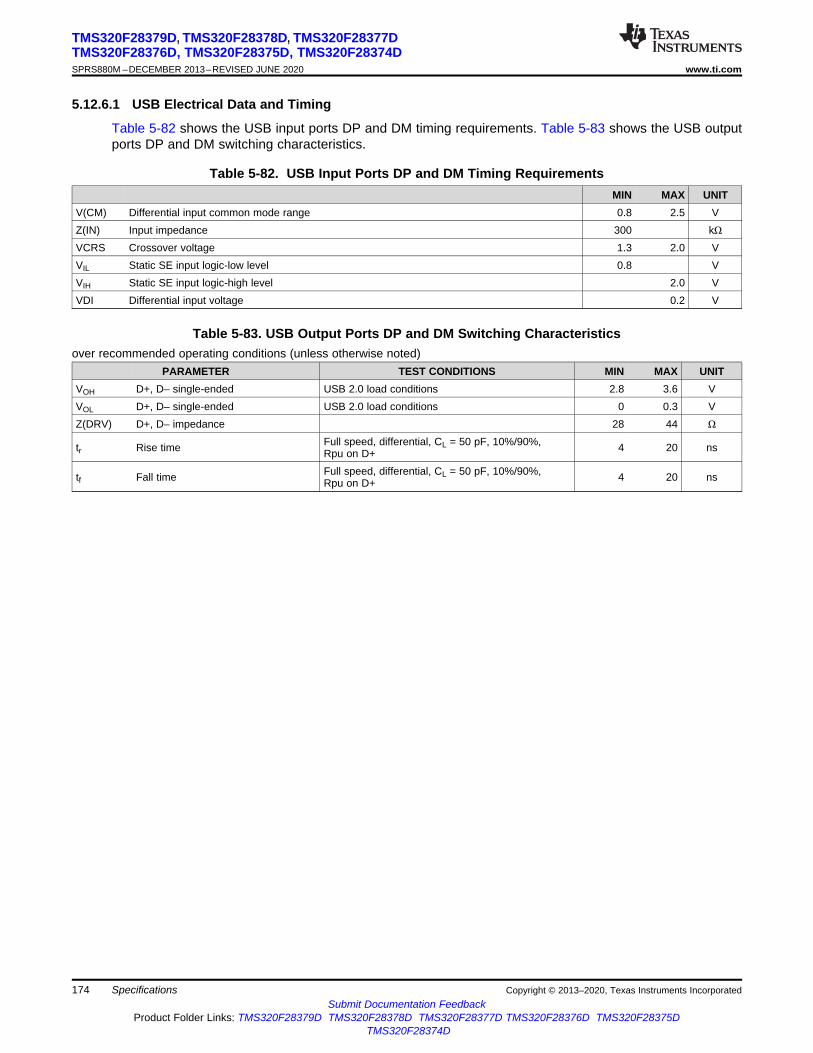
174
TMS320F28379D, TMS320F28378D, TMS320F28377DTMS320F28376D, TMS320F28375D, TMS320F28374DSPRS880M –DECEMBER 2013–REVISED JUNE 2020 www.ti.com
Submit Documentation FeedbackProduct Folder Links: TMS320F28379D TMS320F28378D TMS320F28377D TMS320F28376D TMS320F28375D
TMS320F28374D
Specifications Copyright © 2013–2020, Texas Instruments Incorporated
5.12.6.1 USB Electrical Data and Timing
Table 5-82 shows the USB input ports DP and DM timing requirements. Table 5-83 shows the USB outputports DP and DM switching characteristics.
Table 5-82. USB Input Ports DP and DM Timing RequirementsMIN MAX UNIT
V(CM) Differential input common mode range 0.8 2.5 VZ(IN) Input impedance 300 kΩVCRS Crossover voltage 1.3 2.0 VVIL Static SE input logic-low level 0.8 VVIH Static SE input logic-high level 2.0 VVDI Differential input voltage 0.2 V
Table 5-83. USB Output Ports DP and DM Switching Characteristicsover recommended operating conditions (unless otherwise noted)
PARAMETER TEST CONDITIONS MIN MAX UNITVOH D+, D– single-ended USB 2.0 load conditions 2.8 3.6 VVOL D+, D– single-ended USB 2.0 load conditions 0 0.3 VZ(DRV) D+, D– impedance 28 44 Ω
tr Rise time Full speed, differential, CL = 50 pF, 10%/90%,Rpu on D+ 4 20 ns
tf Fall time Full speed, differential, CL = 50 pF, 10%/90%,Rpu on D+ 4 20 ns
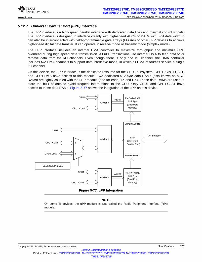
CPU1.CLA1
CPU1.DMA
Arbi
t
Arbiter X
SECMSEL.PF2SEL
uPP
(Universal
Parallel Port)
RX-DATARAM
512 Byte
(Dual Port
Memory)
TX-DATARAM
512 Byte
(Dual Port
Memory)
Arbi
t
CPU1
Arbiter Y
0
1
Arbi
t
Arbiter Y
CPU1
CPU1.CLA1
CPU1
CPU1.CLA1
WRITE
READ
I/O Interface
uPP DMA READ
uPP DMA WRITE
175
TMS320F28379D, TMS320F28378D, TMS320F28377DTMS320F28376D, TMS320F28375D, TMS320F28374D
www.ti.com SPRS880M –DECEMBER 2013–REVISED JUNE 2020
Submit Documentation FeedbackProduct Folder Links: TMS320F28379D TMS320F28378D TMS320F28377D TMS320F28376D TMS320F28375D
TMS320F28374D
SpecificationsCopyright © 2013–2020, Texas Instruments Incorporated
5.12.7 Universal Parallel Port (uPP) InterfaceThe uPP interface is a high-speed parallel interface with dedicated data lines and minimal control signals.The uPP interface is designed to interface cleanly with high-speed ADCs or DACs with 8-bit data width. Itcan also be interconnected with field-programmable gate arrays (FPGAs) or other uPP devices to achievehigh-speed digital data transfer. It can operate in receive mode or transmit mode (simplex mode).
The uPP interface includes an internal DMA controller to maximize throughput and minimize CPUoverhead during high-speed data transmission. All uPP transactions use internal DMA to feed data to orretrieve data from the I/O channels. Even though there is only one I/O channel, the DMA controllerincludes two DMA channels to support data interleave mode, in which all DMA resources service a singleI/O channel.
On this device, the uPP interface is the dedicated resource for the CPU1 subsystem. CPU1, CPU1.CLA1,and CPU1.DMA have access to this module. Two dedicated 512-byte data RAMs (also known as MSGRAMs) are tightly coupled with the uPP module (one for each, TX and RX). These data RAMs are used tostore the bulk of data to avoid frequent interruptions to the CPU. Only CPU1 and CPU1.CLA1 haveaccess to these data RAMs. Figure 5-77 shows the integration of the uPP on this device.
Figure 5-77. uPP Integration
NOTEOn some TI devices, the uPP module is also called the Radio Peripheral Interface (RPI)module.

Arbit
Internal
DMA
Arbi
tI-FIFO
ArbiQ-FIFO
Data Interleaving
(TX/RX)
64 Bit
MEM WR I/F
64 Bit
MEM RD I/F
Transmit Timing
and Control
CLKDIVIDERCPU1.SYSCLK
Receive Timing
and ControlInterrupt/Trigger
Configuration
I/FG
P
I
O
M
U
X
and
I/O
C
O
N
T
R
O
L
ENABLE OUT
START OUT
WAIT IN
ENABLE IN
START IN
WAIT OUT
ENABLE/GPIOx
START/GPIOx
WAIT/GPIOx
CLK OUT
CLK IN
CLK/GPIOx
DATA OUT
DATA IN
DATA[7:0]/GPIOx
uPP
Control Mux
MMR
176
TMS320F28379D, TMS320F28378D, TMS320F28377DTMS320F28376D, TMS320F28375D, TMS320F28374DSPRS880M –DECEMBER 2013–REVISED JUNE 2020 www.ti.com
Submit Documentation FeedbackProduct Folder Links: TMS320F28379D TMS320F28378D TMS320F28377D TMS320F28376D TMS320F28375D
TMS320F28374D
Specifications Copyright © 2013–2020, Texas Instruments Incorporated
The uPP interface supports the following:• Mainstream high-speed data converters with parallel conversion interface.• Mainstream high-speed streaming interface with frame START indication.• Mainstream high-speed streaming interface with data ENABLE indication.• Mainstream high-speed streaming interface with synchronization WAIT signal.• SDR (single-data-rate) or DDR (double-data-rate, interleaved) interface.• Multiplexing of interleaved data in SDR transmit case.• Demultiplexing and multiplexing of interleaved data in DDR case.• I/O interface clock frequency up to 50 MHz for SDR, and 25 MHz for DDR.• Single-channel 8-bit input receive or output transmit mode.• Max throughput is 50MB/s for pure read or pure write.• Available as a DSP to FPGA general-purpose streaming interface.
Figure 5-78 shows the uPP functional block diagram.
Figure 5-78. uPP Functional Block Diagram
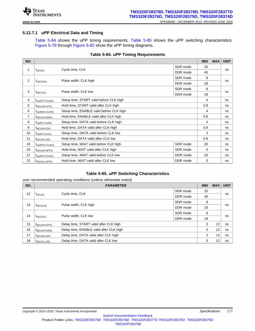
177
TMS320F28379D, TMS320F28378D, TMS320F28377DTMS320F28376D, TMS320F28375D, TMS320F28374D
www.ti.com SPRS880M –DECEMBER 2013–REVISED JUNE 2020
Submit Documentation FeedbackProduct Folder Links: TMS320F28379D TMS320F28378D TMS320F28377D TMS320F28376D TMS320F28375D
TMS320F28374D
SpecificationsCopyright © 2013–2020, Texas Instruments Incorporated
5.12.7.1 uPP Electrical Data and Timing
Table 5-84 shows the uPP timing requirements. Table 5-85 shows the uPP switching characteristics.Figure 5-79 through Figure 5-82 show the uPP timing diagrams.
Table 5-84. uPP Timing RequirementsNO. MIN MAX UNIT
1 tc(CLK) Cycle time, CLKSDR mode 20
nsDDR mode 40
2 tw(CLKH) Pulse width, CLK highSDR mode 8
nsDDR mode 18
3 tw(CLKL) Pulse width, CLK lowSDR mode 8
nsDDR mode 18
4 tsu(STV-CLKH) Setup time, START valid before CLK high 4 ns5 th(CLKH-STV) Hold time, START valid after CLK high 0.8 ns6 tsu(ENV-CLKH) Setup time, ENABLE valid before CLK high 4 ns7 th(CLKH-ENV) Hold time, ENABLE valid after CLK high 0.8 ns8 tsu(DV-CLKH) Setup time, DATA valid before CLK high 4 ns9 th(CLKH-DV) Hold time, DATA valid after CLK high 0.8 ns10 tsu(DV-CLKL) Setup time, DATA valid before CLK low 4 ns11 th(CLKL-DV) Hold time, DATA valid after CLK low 0.8 ns19 tsu(WTV-CLKH) Setup time, WAIT valid before CLK high SDR mode 20 ns20 th(CLKH-WTV) Hold time, WAIT valid after CLK high SDR mode 0 ns21 tsu(WTV-CLKL) Setup time, WAIT valid before CLK low DDR mode 20 ns22 th(CLKL-WTV) Hold time, WAIT valid after CLK low DDR mode 0 ns
Table 5-85. uPP Switching Characteristicsover recommended operating conditions (unless otherwise noted)
NO. PARAMETER MIN MAX UNIT
12 tc(CLK) Cycle time, CLKSDR mode 20
nsDDR mode 40
13 tw(CLKH) Pulse width, CLK highSDR mode 8
nsDDR mode 18
14 tw(CLKL) Pulse width, CLK lowSDR mode 8
nsDDR mode 18
15 td(CLKH-STV) Delay time, START valid after CLK high 3 12 ns16 td(CLKH-ENV) Delay time, ENABLE valid after CLK high 3 12 ns17 td(CLKH-DV) Delay time, DATA valid after CLK high 3 12 ns18 td(CLKL-DV) Delay time, DATA valid after CLK low 3 12 ns
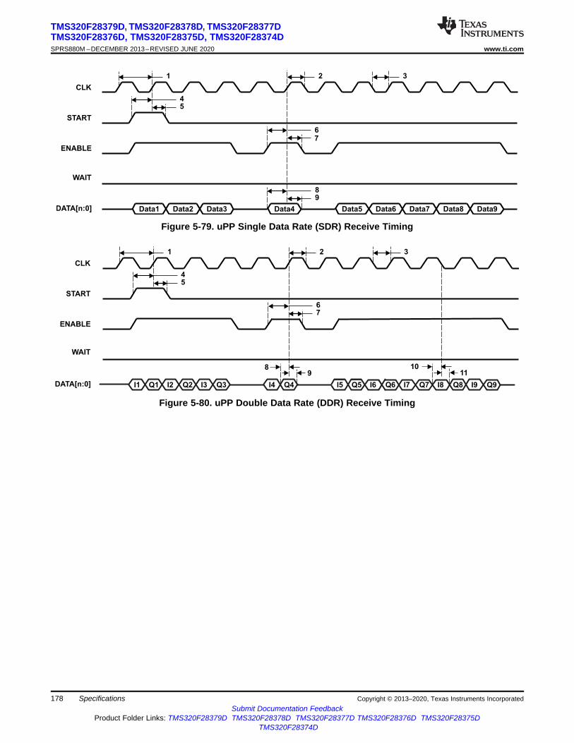
I1
21 3
54
76
9
Q1 I2 I3 I4 I5 I6 I7 I8 I9Q2 Q3 Q4 Q5 Q6 Q7 Q8 Q9
8
CLK
START
ENABLE
DATA[n:0]
WAIT
1110
CLK
START
ENABLE
DATA[n:0] Data2Data1 Data3 Data4
2
WAIT
Data5 Data6
1
Data7 Data8 Data9
3
54
76
98
178
TMS320F28379D, TMS320F28378D, TMS320F28377DTMS320F28376D, TMS320F28375D, TMS320F28374DSPRS880M –DECEMBER 2013–REVISED JUNE 2020 www.ti.com
Submit Documentation FeedbackProduct Folder Links: TMS320F28379D TMS320F28378D TMS320F28377D TMS320F28376D TMS320F28375D
TMS320F28374D
Specifications Copyright © 2013–2020, Texas Instruments Incorporated
Figure 5-79. uPP Single Data Rate (SDR) Receive Timing
Figure 5-80. uPP Double Data Rate (DDR) Receive Timing

I1
15
13
17
16
12 14
2221
Q1 I2 I3 I4 I5 I6 I7 I8 I9Q2 Q3 Q4 Q5 Q6 Q7 Q8 Q9
18
CLK
START
ENABLE
DATA[n:0]
WAIT
Data2Data1 Data3 Data4
15
13
17
16
Data5 Data6
12
Data7 Data8 Data9
14
2019
CLK
START
ENABLE
DATA[n:0]
WAIT
179
TMS320F28379D, TMS320F28378D, TMS320F28377DTMS320F28376D, TMS320F28375D, TMS320F28374D
www.ti.com SPRS880M –DECEMBER 2013–REVISED JUNE 2020
Submit Documentation FeedbackProduct Folder Links: TMS320F28379D TMS320F28378D TMS320F28377D TMS320F28376D TMS320F28375D
TMS320F28374D
SpecificationsCopyright © 2013–2020, Texas Instruments Incorporated
Figure 5-81. uPP Single Data Rate (SDR) Transmit Timing
Figure 5-82. uPP Double Data Rate (DDR) Transmit Timing
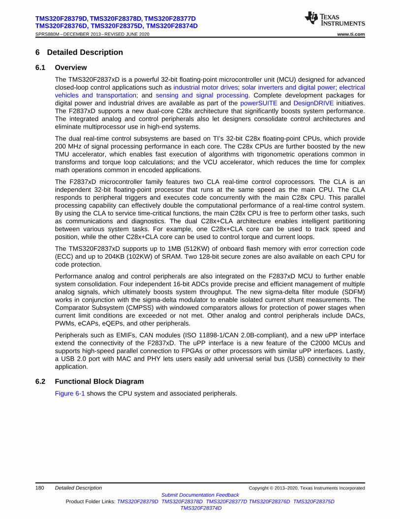
180
TMS320F28379D, TMS320F28378D, TMS320F28377DTMS320F28376D, TMS320F28375D, TMS320F28374DSPRS880M –DECEMBER 2013–REVISED JUNE 2020 www.ti.com
Submit Documentation FeedbackProduct Folder Links: TMS320F28379D TMS320F28378D TMS320F28377D TMS320F28376D TMS320F28375D
TMS320F28374D
Detailed Description Copyright © 2013–2020, Texas Instruments Incorporated
6 Detailed Description
6.1 OverviewThe TMS320F2837xD is a powerful 32-bit floating-point microcontroller unit (MCU) designed for advancedclosed-loop control applications such as industrial motor drives; solar inverters and digital power; electricalvehicles and transportation; and sensing and signal processing. Complete development packages fordigital power and industrial drives are available as part of the powerSUITE and DesignDRIVE initiatives.The F2837xD supports a new dual-core C28x architecture that significantly boosts system performance.The integrated analog and control peripherals also let designers consolidate control architectures andeliminate multiprocessor use in high-end systems.
The dual real-time control subsystems are based on TI’s 32-bit C28x floating-point CPUs, which provide200 MHz of signal processing performance in each core. The C28x CPUs are further boosted by the newTMU accelerator, which enables fast execution of algorithms with trigonometric operations common intransforms and torque loop calculations; and the VCU accelerator, which reduces the time for complexmath operations common in encoded applications.
The F2837xD microcontroller family features two CLA real-time control coprocessors. The CLA is anindependent 32-bit floating-point processor that runs at the same speed as the main CPU. The CLAresponds to peripheral triggers and executes code concurrently with the main C28x CPU. This parallelprocessing capability can effectively double the computational performance of a real-time control system.By using the CLA to service time-critical functions, the main C28x CPU is free to perform other tasks, suchas communications and diagnostics. The dual C28x+CLA architecture enables intelligent partitioningbetween various system tasks. For example, one C28x+CLA core can be used to track speed andposition, while the other C28x+CLA core can be used to control torque and current loops.
The TMS320F2837xD supports up to 1MB (512KW) of onboard flash memory with error correction code(ECC) and up to 204KB (102KW) of SRAM. Two 128-bit secure zones are also available on each CPU forcode protection.
Performance analog and control peripherals are also integrated on the F2837xD MCU to further enablesystem consolidation. Four independent 16-bit ADCs provide precise and efficient management of multipleanalog signals, which ultimately boosts system throughput. The new sigma-delta filter module (SDFM)works in conjunction with the sigma-delta modulator to enable isolated current shunt measurements. TheComparator Subsystem (CMPSS) with windowed comparators allows for protection of power stages whencurrent limit conditions are exceeded or not met. Other analog and control peripherals include DACs,PWMs, eCAPs, eQEPs, and other peripherals.
Peripherals such as EMIFs, CAN modules (ISO 11898-1/CAN 2.0B-compliant), and a new uPP interfaceextend the connectivity of the F2837xD. The uPP interface is a new feature of the C2000 MCUs andsupports high-speed parallel connection to FPGAs or other processors with similar uPP interfaces. Lastly,a USB 2.0 port with MAC and PHY lets users easily add universal serial bus (USB) connectivity to theirapplication.
6.2 Functional Block DiagramFigure 6-1 shows the CPU system and associated peripherals.
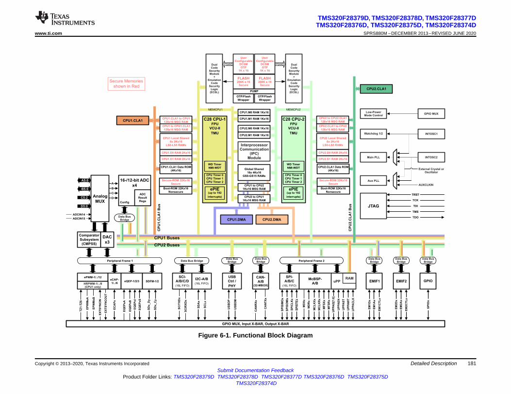
16-/12-bit ADC
x4
Analog
MUX
ADC
Result
Regs
Peripheral Frame 1
Global Shared
16x 4Kx16
GS0-GS15 RAMs
CPU1 to CPU2
1Kx16 MSG RAM
GPIO MUX, Input X-BAR, Output X-BAR
CPU1.M0 RAM 1Kx16
CPU1.M1 RAM 1Kx16
CPU2.M0 RAM 1Kx16
CPU2.M1 RAM 1Kx16
PSWDPSWD
Secure Memories
shown in Red
MEMCPU2
CPU2 to CPU1
1Kx16 MSG RAM
MEMCPU1
CPU1 Buses
CPU2 Buses
A5:0
B5:0
C5:2
ADCIN14
ADCIN15
D5:0
Comparator
Subsystem
(CMPSS)
DAC
x3
Config
CP
U1
.CL
A1
Bu
s
CP
U2
.CL
A1
Bu
s
C28 CPU-1FPU
VCU-II
TMU
CPU Timer 0
CPU Timer 1
CPU Timer 2
ePIE(up to 192
interrupts)
WD Timer
NMI-WDT
C28 CPU-2FPU
VCU-II
TMU
CPU Timer 0
CPU Timer 1
CPU Timer 2
ePIE(up to 192
interrupts)
WD Timer
NMI-WDTCPU1.CLA1 Data ROM
(4Kx16)
CPU1.CLA1 to CPU1
128x16 MSG RAM
CPU1 to CPU1.CLA1
128x16 MSG RAM
CPU1.D0 RAM 2Kx16
CPU1.D1 RAM 2Kx16
Boot-ROM 32Kx16
Nonsecure
Secure-ROM 32Kx16
Secure
CPU1 Local Shared
6x 2Kx16
LS0-LS5 RAMs
CPU2 to CPU2.CLA1
128x16 MSG RAM
CPU2.CLA1 to CPU2
128x16 MSG RAM
CPU2.D0 RAM 2Kx16
CPU2.D1 RAM 2Kx16
CPU2.CLA1 Data ROM
(4Kx16)
Boot-ROM 32Kx16
Nonsecure
Secure-ROM 32Kx16
Secure
CPU2 Local Shared
LS0-LS5 RAMs
CPU1.CLA1
CPU1.DMA CPU2.DMA
CPU2.CLA1
Data BusBridge
ePWM-1/../12eCAP-
1/../6eQEP-1/2/3 SDFM-1/2
EX
TS
YN
CIN
EX
TS
YN
CO
UT
TZ
1-T
Z6
EC
AP
x
EQ
EP
xA
EQ
EP
xB
EP
WM
xA
EP
WM
xB
EQ
EP
xI
EQ
EP
xS
SD
x_
Dy
SD
x_
Cy
A
B
C
D
JTAG
AUXCLKIN
External Crystal orOscillator
Watchdog 1/2
Main PLL
Aux PLL
INTOSC1
INTOSC2
Low-PowerMode Control
GPIO MUX
TRST
TCK
TDI
TMS
TDO
6x 2Kx16
DualCode
SecurityModule
+Emulation
CodeSecurity
Logic(ECSL)
DualCode
SecurityModule
+Emulation
CodeSecurity
Logic(ECSL)
InterprocessorCommunication
(IPC)Module
PUMP
OTP/Flash
Wrapper
FLASH256K x 16
Secure
UserConfigurable
DCSMOTP
1K x 16
OTP/Flash
Wrapper
FLASH256K x 16
Secure
UserConfigurable
DCSMOTP
1K x 16
SCI-
A/B/C/D
(16L FIFO)
I2C-A/B
(16L FIFO)
Data Bus Bridge
SC
ITX
Dx
SC
IRX
Dx
SD
Ax
SC
Lx
CAN-
A/B(32-MBOX)
Data BusBridge
CA
NR
Xx
CA
NT
Xx
GPIO
Data BusBridge
GP
IOn
Data BusBridge
USB
Ctrl /
PHY
US
BD
P
US
BD
M
USB
Ctrl /
PHY
EMIF1
Data BusBridge
EM
1D
x
EM
1A
x
EM
1C
TL
x
EMIF2
Data BusBridge
EM
2D
x
EM
2A
x
EM
2C
TL
x
Peripheral Frame 2
SPI-
A/B/C
(16L FIFO)
SP
ISIM
Ox
SP
ISO
MIx
SP
ICL
Kx
SP
IST
Ex
McBSP-
A/B
MD
Xx
MD
Rx
MC
LK
Xx
MC
LK
Rx
MF
SX
x
MF
SR
x
uPPRAM
UP
PA
D[7
:0]
UP
PA
EN
UP
PA
ST
UP
PA
WT
UP
PA
CL
K
HRPWM-1/../8(CPU1 only)
Copyright © 2013–2020, Texas Instruments Incorporated Detailed DescriptionSubmit Documentation Feedback
Product Folder Links: TMS320F28379D TMS320F28378D TMS320F28377D TMS320F28376D TMS320F28375DTMS320F28374D
181
TMS320F28379D, TMS320F28378D, TMS320F28377DTMS320F28376D, TMS320F28375D, TMS320F28374D
www.ti.com SPRS880M –DECEMBER 2013–REVISED JUNE 2020
Figure 6-1. Functional Block Diagram

182
TMS320F28379D, TMS320F28378D, TMS320F28377DTMS320F28376D, TMS320F28375D, TMS320F28374DSPRS880M –DECEMBER 2013–REVISED JUNE 2020 www.ti.com
Submit Documentation FeedbackProduct Folder Links: TMS320F28379D TMS320F28378D TMS320F28377D TMS320F28376D TMS320F28375D
TMS320F28374D
Detailed Description Copyright © 2013–2020, Texas Instruments Incorporated
(1) Shared between CPU subsystems.(2) Available only on F28379D, F28378D, F28377D, and F28375D.
6.3 Memory
6.3.1 C28x Memory MapBoth C28x CPUs on the device have the same memory map except where noted in Table 6-1. TheGSx_RAM (Global Shared RAM) should be assigned to either CPU by the GSxMSEL register. Memoriesaccessible by the CLA or DMA (direct memory access) are noted as well.
Table 6-1. C28x Memory MapMEMORY SIZE START ADDRESS END ADDRESS CLA ACCESS DMA ACCESS
M0 RAM 1K × 16 0x0000 0000 0x0000 03FF
M1 RAM 1K × 16 0x0000 0400 0x0000 07FF
PieVectTable 512 × 16 0x0000 0D00 0x0000 0EFF
CPUx.CLA1 to CPUx MSGRAM 128 × 16 0x0000 1480 0x0000 14FF Yes
CPUx to CPUx.CLA1 MSGRAM 128 × 16 0x0000 1500 0x0000 157F Yes
UPP TX MSG RAM 512 × 16 0x0000 6C00 0x0000 6DFF Yes(CPU1.CLA1 only)
UPP RX MSG RAM 512 × 16 0x0000 6E00 0x0000 6FFF Yes(CPU1.CLA1 only)
LS0 RAM 2K × 16 0x0000 8000 0x0000 87FF Yes
LS1 RAM 2K × 16 0x0000 8800 0x0000 8FFF Yes
LS2 RAM 2K × 16 0x0000 9000 0x0000 97FF Yes
LS3 RAM 2K × 16 0x0000 9800 0x0000 9FFF Yes
LS4 RAM 2K × 16 0x0000 A000 0x0000 A7FF Yes
LS5 RAM 2K × 16 0x0000 A800 0x0000 AFFF Yes
D0 RAM 2K × 16 0x0000 B000 0x0000 B7FF
D1 RAM 2K × 16 0x0000 B800 0x0000 BFFF
GS0 RAM (1) 4K × 16 0x0000 C000 0x0000 CFFF Yes
GS1 RAM (1) 4K × 16 0x0000 D000 0x0000 DFFF Yes
GS2 RAM (1) 4K × 16 0x0000 E000 0x0000 EFFF Yes
GS3 RAM (1) 4K × 16 0x0000 F000 0x0000 FFFF Yes
GS4 RAM (1) 4K × 16 0x0001 0000 0x0001 0FFF Yes
GS5 RAM (1) 4K × 16 0x0001 1000 0x0001 1FFF Yes
GS6 RAM (1) 4K × 16 0x0001 2000 0x0001 2FFF Yes
GS7 RAM (1) 4K × 16 0x0001 3000 0x0001 3FFF Yes
GS8 RAM (1) 4K × 16 0x0001 4000 0x0001 4FFF Yes
GS9 RAM (1) 4K × 16 0x0001 5000 0x0001 5FFF Yes
GS10 RAM (1) 4K × 16 0x0001 6000 0x0001 6FFF Yes
GS11 RAM (1) 4K × 16 0x0001 7000 0x0001 7FFF Yes
GS12 RAM (1) (2) 4K × 16 0x0001 8000 0x0001 8FFF Yes
GS13 RAM (1) (2) 4K × 16 0x0001 9000 0x0001 9FFF Yes
GS14 RAM (1) (2) 4K × 16 0x0001 A000 0x0001 AFFF Yes
GS15 RAM (1) (2) 4K × 16 0x0001 B000 0x0001 BFFF Yes
CPU2 to CPU1 MSGRAM (1) 1K × 16 0x0003 F800 0x0003 FBFF Yes
CPU1 to CPU2 MSGRAM (1) 1K × 16 0x0003 FC00 0x0003 FFFF Yes
CAN A Message RAM (1) 2K × 16 0x0004 9000 0x0004 97FF
CAN B Message RAM (1) 2K × 16 0x0004 B000 0x0004 B7FF
Flash 256K × 16 0x0008 0000 0x000B FFFF
Secure ROM 32K × 16 0x003F 0000 0x003F 7FFF
Boot ROM 32K × 16 0x003F 8000 0x003F FFBF
Vectors 64 × 16 0x003F FFC0 0x003F FFFF
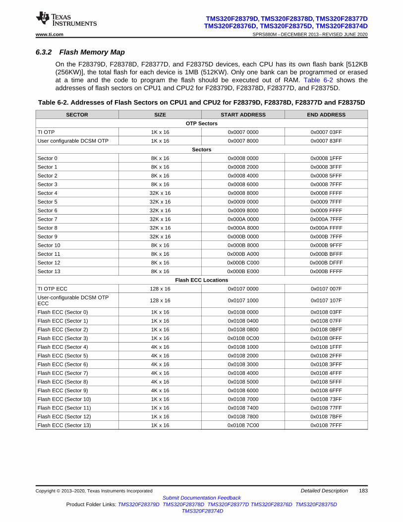
183
TMS320F28379D, TMS320F28378D, TMS320F28377DTMS320F28376D, TMS320F28375D, TMS320F28374D
www.ti.com SPRS880M –DECEMBER 2013–REVISED JUNE 2020
Submit Documentation FeedbackProduct Folder Links: TMS320F28379D TMS320F28378D TMS320F28377D TMS320F28376D TMS320F28375D
TMS320F28374D
Detailed DescriptionCopyright © 2013–2020, Texas Instruments Incorporated
6.3.2 Flash Memory MapOn the F28379D, F28378D, F28377D, and F28375D devices, each CPU has its own flash bank [512KB(256KW)], the total flash for each device is 1MB (512KW). Only one bank can be programmed or erasedat a time and the code to program the flash should be executed out of RAM. Table 6-2 shows theaddresses of flash sectors on CPU1 and CPU2 for F28379D, F28378D, F28377D, and F28375D.
Table 6-2. Addresses of Flash Sectors on CPU1 and CPU2 for F28379D, F28378D, F28377D and F28375D
SECTOR SIZE START ADDRESS END ADDRESSOTP Sectors
TI OTP 1K x 16 0x0007 0000 0x0007 03FFUser configurable DCSM OTP 1K x 16 0x0007 8000 0x0007 83FF
SectorsSector 0 8K x 16 0x0008 0000 0x0008 1FFFSector 1 8K x 16 0x0008 2000 0x0008 3FFFSector 2 8K x 16 0x0008 4000 0x0008 5FFFSector 3 8K x 16 0x0008 6000 0x0008 7FFFSector 4 32K x 16 0x0008 8000 0x0008 FFFFSector 5 32K x 16 0x0009 0000 0x0009 7FFFSector 6 32K x 16 0x0009 8000 0x0009 FFFFSector 7 32K x 16 0x000A 0000 0x000A 7FFFSector 8 32K x 16 0x000A 8000 0x000A FFFFSector 9 32K x 16 0x000B 0000 0x000B 7FFFSector 10 8K x 16 0x000B 8000 0x000B 9FFFSector 11 8K x 16 0x000B A000 0x000B BFFFSector 12 8K x 16 0x000B C000 0x000B DFFFSector 13 8K x 16 0x000B E000 0x000B FFFF
Flash ECC LocationsTI OTP ECC 128 x 16 0x0107 0000 0x0107 007FUser-configurable DCSM OTPECC 128 x 16 0x0107 1000 0x0107 107F
Flash ECC (Sector 0) 1K x 16 0x0108 0000 0x0108 03FFFlash ECC (Sector 1) 1K x 16 0x0108 0400 0x0108 07FFFlash ECC (Sector 2) 1K x 16 0x0108 0800 0x0108 0BFFFlash ECC (Sector 3) 1K x 16 0x0108 0C00 0x0108 0FFFFlash ECC (Sector 4) 4K x 16 0x0108 1000 0x0108 1FFFFlash ECC (Sector 5) 4K x 16 0x0108 2000 0x0108 2FFFFlash ECC (Sector 6) 4K x 16 0x0108 3000 0x0108 3FFFFlash ECC (Sector 7) 4K x 16 0x0108 4000 0x0108 4FFFFlash ECC (Sector 8) 4K x 16 0x0108 5000 0x0108 5FFFFlash ECC (Sector 9) 4K x 16 0x0108 6000 0x0108 6FFFFlash ECC (Sector 10) 1K x 16 0x0108 7000 0x0108 73FFFlash ECC (Sector 11) 1K x 16 0x0108 7400 0x0108 77FFFlash ECC (Sector 12) 1K x 16 0x0108 7800 0x0108 7BFFFlash ECC (Sector 13) 1K x 16 0x0108 7C00 0x0108 7FFF
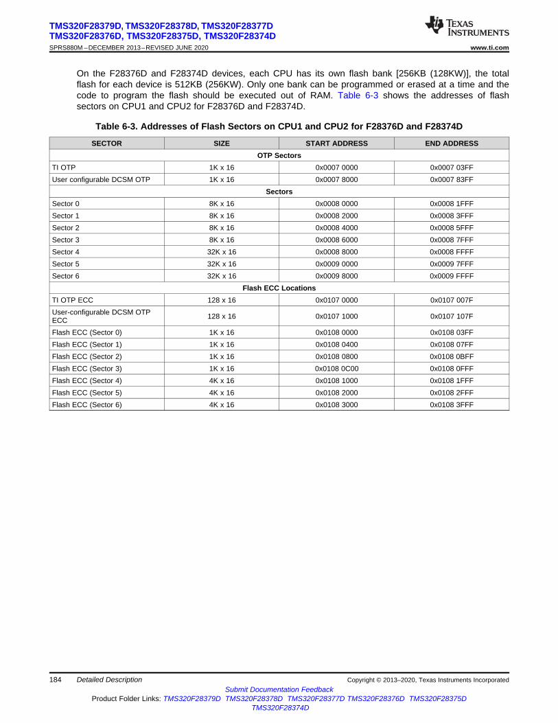
184
TMS320F28379D, TMS320F28378D, TMS320F28377DTMS320F28376D, TMS320F28375D, TMS320F28374DSPRS880M –DECEMBER 2013–REVISED JUNE 2020 www.ti.com
Submit Documentation FeedbackProduct Folder Links: TMS320F28379D TMS320F28378D TMS320F28377D TMS320F28376D TMS320F28375D
TMS320F28374D
Detailed Description Copyright © 2013–2020, Texas Instruments Incorporated
On the F28376D and F28374D devices, each CPU has its own flash bank [256KB (128KW)], the totalflash for each device is 512KB (256KW). Only one bank can be programmed or erased at a time and thecode to program the flash should be executed out of RAM. Table 6-3 shows the addresses of flashsectors on CPU1 and CPU2 for F28376D and F28374D.
Table 6-3. Addresses of Flash Sectors on CPU1 and CPU2 for F28376D and F28374D
SECTOR SIZE START ADDRESS END ADDRESSOTP Sectors
TI OTP 1K x 16 0x0007 0000 0x0007 03FFUser configurable DCSM OTP 1K x 16 0x0007 8000 0x0007 83FF
SectorsSector 0 8K x 16 0x0008 0000 0x0008 1FFFSector 1 8K x 16 0x0008 2000 0x0008 3FFFSector 2 8K x 16 0x0008 4000 0x0008 5FFFSector 3 8K x 16 0x0008 6000 0x0008 7FFFSector 4 32K x 16 0x0008 8000 0x0008 FFFFSector 5 32K x 16 0x0009 0000 0x0009 7FFFSector 6 32K x 16 0x0009 8000 0x0009 FFFF
Flash ECC LocationsTI OTP ECC 128 x 16 0x0107 0000 0x0107 007FUser-configurable DCSM OTPECC 128 x 16 0x0107 1000 0x0107 107F
Flash ECC (Sector 0) 1K x 16 0x0108 0000 0x0108 03FFFlash ECC (Sector 1) 1K x 16 0x0108 0400 0x0108 07FFFlash ECC (Sector 2) 1K x 16 0x0108 0800 0x0108 0BFFFlash ECC (Sector 3) 1K x 16 0x0108 0C00 0x0108 0FFFFlash ECC (Sector 4) 4K x 16 0x0108 1000 0x0108 1FFFFlash ECC (Sector 5) 4K x 16 0x0108 2000 0x0108 2FFFFlash ECC (Sector 6) 4K x 16 0x0108 3000 0x0108 3FFF

185
TMS320F28379D, TMS320F28378D, TMS320F28377DTMS320F28376D, TMS320F28375D, TMS320F28374D
www.ti.com SPRS880M –DECEMBER 2013–REVISED JUNE 2020
Submit Documentation FeedbackProduct Folder Links: TMS320F28379D TMS320F28378D TMS320F28377D TMS320F28376D TMS320F28375D
TMS320F28374D
Detailed DescriptionCopyright © 2013–2020, Texas Instruments Incorporated
(1) Available memory size listed in this table is the maximum possible size assuming 32-bit memory. This may not apply to other memorysizes because of pin mux setting. See Section 4.4.1 to find the available address lines for your use case.
(2) The 2M × 16 size is for a 32-bit interface with the assumption that 16-bit accesses are not performed; hence, byte enables are not used(tied to active value on board). If byte enables are used, then the maximum size is smaller because byte enables are muxed withaddress pins (see Section 4.4.1). If 16-bit memory is used, then the maximum size is 1M × 16.
(3) Available only on the CPU1 subsystem.
6.3.3 EMIF Chip Select Memory MapThe EMIF1 memory map is the same for both CPU subsystems. EMIF2 is available only on the CPU1subsystem. The EMIF memory map is shown in Table 6-4.
Table 6-4. EMIF Chip Select Memory Map
EMIF CHIP SELECT SIZE (1) START ADDRESS END ADDRESS CLA ACCESS DMA ACCESSEMIF1_CS0n - Data 256M × 16 0x8000 0000 0x8FFF FFFF YesEMIF1_CS2n - Program + Data (2) 2M × 16 0x0010 0000 0x002F FFFF YesEMIF1_CS3n - Program + Data 512K × 16 0x0030 0000 0x0037 FFFF YesEMIF1_CS4n - Program + Data 393K × 16 0x0038 0000 0x003D FFFF YesEMIF2_CS0n - Data (3) 3M × 16 0x9000 0000 0x91FF FFFFEMIF2_CS2n - Program + Data (3) 4K × 16 0x0000 2000 0x0000 2FFF Yes (Data only)
6.3.4 Peripheral Registers Memory MapThe peripheral registers memory map can be found in Table 6-5. The peripheral registers can be assignedto either the CPU1 or CPU2 subsystems except where noted in Table 6-5. Registers in the peripheralframes share a secondary master (CLA or DMA) selection with all other registers within the sameperipheral frame. See the TMS320F2837xD Dual-Core Microcontrollers Technical Reference Manual fordetails on the CPU subsystem and secondary master selection.
Table 6-5. Peripheral Registers Memory Map
REGISTERS STRUCTURE NAME STARTADDRESS
ENDADDRESS PROTECTED(1) CLA
ACCESSDMA
ACCESS
AdcaResultRegs ADC_RESULT_REGS 0x0000 0B00 0x0000 0B1F Yes Yes
AdcbResultRegs ADC_RESULT_REGS 0x0000 0B20 0x0000 0B3F Yes Yes
AdccResultRegs ADC_RESULT_REGS 0x0000 0B40 0x0000 0B5F Yes Yes
AdcdResultRegs ADC_RESULT_REGS 0x0000 0B60 0x0000 0B7F Yes Yes
CpuTimer0Regs(2) CPUTIMER_REGS 0x0000 0C00 0x0000 0C07
CpuTimer1Regs(2) CPUTIMER_REGS 0x0000 0C08 0x0000 0C0F
CpuTimer2Regs(2) CPUTIMER_REGS 0x0000 0C10 0x0000 0C17
PieCtrlRegs(2)(5) PIE_CTRL_REGS 0x0000 0CE0 0x0000 0CFF
Cla1SoftIntRegs(5) CLA_SOFTINT_REGS 0x0000 0CE0 0x0000 0CFF
Yes –CLA only,no CPUaccess
DmaRegs(2) DMA_REGS 0x0000 1000 0x0000 11FF
Cla1Regs(2) CLA_REGS 0x0000 1400 0x0000 147F
Peripheral Frame 1
EPwm1Regs EPWM_REGS 0x0000 4000 0x0000 40FF Yes Yes Yes
EPwm2Regs EPWM_REGS 0x0000 4100 0x0000 41FF Yes Yes Yes
EPwm3Regs EPWM_REGS 0x0000 4200 0x0000 42FF Yes Yes Yes
EPwm4Regs EPWM_REGS 0x0000 4300 0x0000 43FF Yes Yes Yes
EPwm5Regs EPWM_REGS 0x0000 4400 0x0000 44FF Yes Yes Yes
EPwm6Regs EPWM_REGS 0x0000 4500 0x0000 45FF Yes Yes Yes
EPwm7Regs EPWM_REGS 0x0000 4600 0x0000 46FF Yes Yes Yes
EPwm8Regs EPWM_REGS 0x0000 4700 0x0000 47FF Yes Yes Yes
EPwm9Regs EPWM_REGS 0x0000 4800 0x0000 48FF Yes Yes Yes
EPwm10Regs EPWM_REGS 0x0000 4900 0x0000 49FF Yes Yes Yes
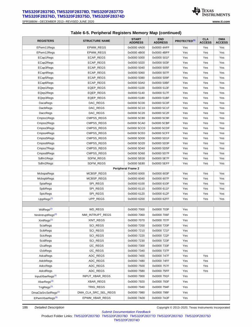
186
TMS320F28379D, TMS320F28378D, TMS320F28377DTMS320F28376D, TMS320F28375D, TMS320F28374DSPRS880M –DECEMBER 2013–REVISED JUNE 2020 www.ti.com
Submit Documentation FeedbackProduct Folder Links: TMS320F28379D TMS320F28378D TMS320F28377D TMS320F28376D TMS320F28375D
TMS320F28374D
Detailed Description Copyright © 2013–2020, Texas Instruments Incorporated
Table 6-5. Peripheral Registers Memory Map (continued)
REGISTERS STRUCTURE NAME STARTADDRESS
ENDADDRESS PROTECTED(1) CLA
ACCESSDMA
ACCESS
EPwm11Regs EPWM_REGS 0x0000 4A00 0x0000 4AFF Yes Yes Yes
EPwm12Regs EPWM_REGS 0x0000 4B00 0x0000 4BFF Yes Yes Yes
ECap1Regs ECAP_REGS 0x0000 5000 0x0000 501F Yes Yes Yes
ECap2Regs ECAP_REGS 0x0000 5020 0x0000 503F Yes Yes Yes
ECap3Regs ECAP_REGS 0x0000 5040 0x0000 505F Yes Yes Yes
ECap4Regs ECAP_REGS 0x0000 5060 0x0000 507F Yes Yes Yes
ECap5Regs ECAP_REGS 0x0000 5080 0x0000 509F Yes Yes Yes
ECap6Regs ECAP_REGS 0x0000 50A0 0x0000 50BF Yes Yes Yes
EQep1Regs EQEP_REGS 0x0000 5100 0x0000 513F Yes Yes Yes
EQep2Regs EQEP_REGS 0x0000 5140 0x0000 517F Yes Yes Yes
EQep3Regs EQEP_REGS 0x0000 5180 0x0000 51BF Yes Yes Yes
DacaRegs DAC_REGS 0x0000 5C00 0x0000 5C0F Yes Yes Yes
DacbRegs DAC_REGS 0x0000 5C10 0x0000 5C1F Yes Yes Yes
DaccRegs DAC_REGS 0x0000 5C20 0x0000 5C2F Yes Yes Yes
Cmpss1Regs CMPSS_REGS 0x0000 5C80 0x0000 5C9F Yes Yes Yes
Cmpss2Regs CMPSS_REGS 0x0000 5CA0 0x0000 5CBF Yes Yes Yes
Cmpss3Regs CMPSS_REGS 0x0000 5CC0 0x0000 5CDF Yes Yes Yes
Cmpss4Regs CMPSS_REGS 0x0000 5CE0 0x0000 5CFF Yes Yes Yes
Cmpss5Regs CMPSS_REGS 0x0000 5D00 0x0000 5D1F Yes Yes Yes
Cmpss6Regs CMPSS_REGS 0x0000 5D20 0x0000 5D3F Yes Yes Yes
Cmpss7Regs CMPSS_REGS 0x0000 5D40 0x0000 5D5F Yes Yes Yes
Cmpss8Regs CMPSS_REGS 0x0000 5D60 0x0000 5D7F Yes Yes Yes
Sdfm1Regs SDFM_REGS 0x0000 5E00 0x0000 5E7F Yes Yes Yes
Sdfm2Regs SDFM_REGS 0x0000 5E80 0x0000 5EFF Yes Yes Yes
Peripheral Frame 2
McbspaRegs MCBSP_REGS 0x0000 6000 0x0000 603F Yes Yes Yes
McbspbRegs MCBSP_REGS 0x0000 6040 0x0000 607F Yes Yes Yes
SpiaRegs SPI_REGS 0x0000 6100 0x0000 610F Yes Yes Yes
SpibRegs SPI_REGS 0x0000 6110 0x0000 611F Yes Yes Yes
SpicRegs SPI_REGS 0x0000 6120 0x0000 612F Yes Yes Yes
UppRegs(3) UPP_REGS 0x0000 6200 0x0000 62FF Yes Yes Yes
WdRegs(2) WD_REGS 0x0000 7000 0x0000 703F Yes
NmiIntruptRegs(2) NMI_INTRUPT_REGS 0x0000 7060 0x0000 706F Yes
XintRegs(2) XINT_REGS 0x0000 7070 0x0000 707F Yes
SciaRegs SCI_REGS 0x0000 7200 0x0000 720F Yes
ScibRegs SCI_REGS 0x0000 7210 0x0000 721F Yes
ScicRegs SCI_REGS 0x0000 7220 0x0000 722F Yes
ScidRegs SCI_REGS 0x0000 7230 0x0000 723F Yes
I2caRegs I2C_REGS 0x0000 7300 0x0000 733F Yes
I2cbRegs I2C_REGS 0x0000 7340 0x0000 737F Yes
AdcaRegs ADC_REGS 0x0000 7400 0x0000 747F Yes Yes
AdcbRegs ADC_REGS 0x0000 7480 0x0000 74FF Yes Yes
AdccRegs ADC_REGS 0x0000 7500 0x0000 757F Yes Yes
AdcdRegs ADC_REGS 0x0000 7580 0x0000 75FF Yes Yes
InputXbarRegs(3) INPUT_XBAR_REGS 0x0000 7900 0x0000 791F Yes
XbarRegs(3) XBAR_REGS 0x0000 7920 0x0000 793F Yes
TrigRegs(3) TRIG_REGS 0x0000 7940 0x0000 794F Yes
DmaClaSrcSelRegs(2) DMA_CLA_SRC_SEL_REGS 0x0000 7980 0x0000 798F Yes
EPwmXbarRegs(3) EPWM_XBAR_REGS 0x0000 7A00 0x0000 7A3F Yes

187
TMS320F28379D, TMS320F28378D, TMS320F28377DTMS320F28376D, TMS320F28375D, TMS320F28374D
www.ti.com SPRS880M –DECEMBER 2013–REVISED JUNE 2020
Submit Documentation FeedbackProduct Folder Links: TMS320F28379D TMS320F28378D TMS320F28377D TMS320F28376D TMS320F28375D
TMS320F28374D
Detailed DescriptionCopyright © 2013–2020, Texas Instruments Incorporated
Table 6-5. Peripheral Registers Memory Map (continued)
REGISTERS STRUCTURE NAME STARTADDRESS
ENDADDRESS PROTECTED(1) CLA
ACCESSDMA
ACCESS
OutputXbarRegs(3) OUTPUT_XBAR_REGS 0x0000 7A80 0x0000 7ABF Yes
GpioCtrlRegs(3) GPIO_CTRL_REGS 0x0000 7C00 0x0000 7D7F Yes
GpioDataRegs(2) GPIO_DATA_REGS 0x0000 7F00 0x0000 7F2F Yes Yes
UsbaRegs(3) USB_REGS 0x0004 0000 0x0004 0FFF Yes
Emif1Regs EMIF_REGS 0x0004 7000 0x0004 77FF Yes
Emif2Regs(3) EMIF_REGS 0x0004 7800 0x0004 7FFF Yes
CanaRegs CAN_REGS 0x0004 8000 0x0004 87FF Yes
CanbRegs CAN_REGS 0x0004 A000 0x0004 A7FF Yes
IpcRegs(2) IPC_REGS_CPU1IPC_REGS_CPU2 0x0005 0000 0x0005 0023 Yes
FlashPumpSemaphoreRegs(2) FLASH_PUMP_SEMAPHORE_REGS 0x0005 0024 0x0005 0025 Yes
DevCfgRegs(3) DEV_CFG_REGS 0x0005 D000 0x0005 D17F Yes
AnalogSubsysRegs(3) ANALOG_SUBSYS_REGS 0x0005 D180 0x0005 D1FF Yes
ClkCfgRegs(4) CLK_CFG_REGS 0x0005 D200 0x0005 D2FF Yes
CpuSysRegs(2) CPU_SYS_REGS 0x0005 D300 0x0005 D3FF Yes
RomPrefetchRegs(3) ROM_PREFETCH_REGS 0x0005 E608 0x0005 E60B Yes
DcsmZ1Regs(2) DCSM_Z1_REGS 0x0005 F000 0x0005 F02F Yes
DcsmZ2Regs(2) DCSM_Z2_REGS 0x0005 F040 0x0005 F05F Yes
DcsmCommonRegs(2) DCSM_COMMON_REGS 0x0005 F070 0x0005 F07F Yes
MemCfgRegs(2) MEM_CFG_REGS 0x0005 F400 0x0005 F47F Yes
Emif1ConfigRegs(2) EMIF1_CONFIG_REGS 0x0005 F480 0x0005 F49F Yes
Emif2ConfigRegs(3) EMIF2_CONFIG_REGS 0x0005 F4A0 0x0005 F4BF Yes
AccessProtectionRegs(2) ACCESS_PROTECTION_REGS 0x0005 F4C0 0x0005 F4FF Yes
MemoryErrorRegs(2) MEMORY_ERROR_REGS 0x0005 F500 0x0005 F53F Yes
RomWaitStateRegs(3) ROM_WAIT_STATE_REGS 0x0005 F540 0x0005 F541 Yes
Flash0CtrlRegs(2) FLASH_CTRL_REGS 0x0005 F800 0x0005 FAFF Yes
Flash0EccRegs(2) FLASH_ECC_REGS 0x0005 FB00 0x0005 FB3F Yes
(1) The CPU (not applicable for CLA or DMA) contains a write followed by read protection mode to ensure that any read operation thatfollows a write operation within a protected address range is executed as written by delaying the read operation until the write isinitiated.
(2) A unique copy of these registers exist on each CPU subsystem.(3) These registers are available only on the CPU1 subsystem.(4) These registers are mapped to either CPU1 or CPU2 based on a semaphore.(5) The address overlap of PieCtrlRegs and Cla1SoftIntRegs is correct. Each CPU, C28x and CLA, only has access to one of the register
sets.
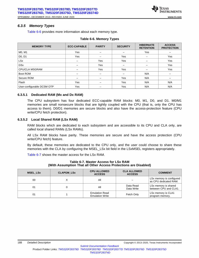
188
TMS320F28379D, TMS320F28378D, TMS320F28377DTMS320F28376D, TMS320F28375D, TMS320F28374DSPRS880M –DECEMBER 2013–REVISED JUNE 2020 www.ti.com
Submit Documentation FeedbackProduct Folder Links: TMS320F28379D TMS320F28378D TMS320F28377D TMS320F28376D TMS320F28375D
TMS320F28374D
Detailed Description Copyright © 2013–2020, Texas Instruments Incorporated
6.3.5 Memory TypesTable 6-6 provides more information about each memory type.
Table 6-6. Memory Types
MEMORY TYPE ECC-CAPABLE PARITY SECURITY HIBERNATERETENTION
ACCESSPROTECTION
M0, M1 Yes – – Yes –D0, D1 Yes – Yes – YesLSx – Yes Yes – YesGSx – Yes – – YesCPU/CLA MSGRAM – Yes Yes – YesBoot ROM – – – N/A –Secure ROM – – Yes N/A –Flash Yes – Yes N/A N/AUser-configurable DCSM OTP Yes – Yes N/A N/A
6.3.5.1 Dedicated RAM (Mx and Dx RAM)
The CPU subsystem has four dedicated ECC-capable RAM blocks: M0, M1, D0, and D1. M0/M1memories are small nonsecure blocks that are tightly coupled with the CPU (that is, only the CPU hasaccess to them). D0/D1 memories are secure blocks and also have the access-protection feature (CPUwrite/CPU fetch protection).
6.3.5.2 Local Shared RAM (LSx RAM)
RAM blocks which are dedicated to each subsystem and are accessible to its CPU and CLA only, arecalled local shared RAMs (LSx RAMs).
All LSx RAM blocks have parity. These memories are secure and have the access protection (CPUwrite/CPU fetch) feature.
By default, these memories are dedicated to the CPU only, and the user could choose to share thesememories with the CLA by configuring the MSEL_LSx bit field in the LSxMSEL registers appropriately.
Table 6-7 shows the master access for the LSx RAM.
Table 6-7. Master Access for LSx RAM(With Assumption That all Other Access Protections are Disabled)
MSEL_LSx CLAPGM_LSx CPU ALLOWEDACCESS
CLA ALLOWEDACCESS COMMENT
00 X All – LSx memory is configuredas CPU dedicated RAM.
01 0 All Data ReadData Write
LSx memory is sharedbetween CPU and CLA1.
01 1 Emulation ReadEmulation Write Fetch Only LSx memory is CLA1
program memory.

189
TMS320F28379D, TMS320F28378D, TMS320F28377DTMS320F28376D, TMS320F28375D, TMS320F28374D
www.ti.com SPRS880M –DECEMBER 2013–REVISED JUNE 2020
Submit Documentation FeedbackProduct Folder Links: TMS320F28379D TMS320F28378D TMS320F28377D TMS320F28376D TMS320F28375D
TMS320F28374D
Detailed DescriptionCopyright © 2013–2020, Texas Instruments Incorporated
6.3.5.3 Global Shared RAM (GSx RAM)
RAM blocks which are accessible from both the CPU and DMA are called global shared RAMs (GSxRAMs). Each shared RAM block can be owned by either CPU subsystem based on the configuration ofrespective bits in the GSxMSEL register.
All GSx RAM blocks have parity.
When a GSx RAM block is owned by a CPU subsystem, the CPUx and CPUx.DMA will have full access tothat RAM block whereas the other CPUy and CPUy.DMA will only have read access (no fetch/writeaccess).
Table 6-8 shows the master access for the GSx RAM.
Table 6-8. Master Access for GSx RAM(With Assumption That all Other Access Protections are Disabled)
GSxMSEL CPU INSTRUCTIONFETCH READ WRITE CPUx.DMA
READCPUx.DMA
WRITE
0CPU1 Yes Yes Yes Yes YesCPU2 – Yes – Yes –
1CPU1 – Yes – Yes –CPU2 Yes Yes Yes Yes Yes
The GSx RAMs have access protection (CPU write/CPU fetch/DMA write).
6.3.5.4 CPU Message RAM (CPU MSGRAM)
These RAM blocks can be used to share data between CPU1 and CPU2. Since these RAMs are used forinterprocessor communication, they are also called IPC RAMs. The CPU MSGRAMs have CPU/DMAread/write access from its own CPU subsystem, and CPU/DMA read only access from the othersubsystem.
This RAM has parity.
6.3.5.5 CLA Message RAM (CLA MSGRAM)
These RAM blocks can be used to share data between the CPU and CLA. The CLA has read and writeaccess to the "CLA to CPU MSGRAM." The CPU has read and write access to the "CPU to CLAMSGRAM." The CPU and CLA both have read access to both MSGRAMs.
This RAM has parity.

190
TMS320F28379D, TMS320F28378D, TMS320F28377DTMS320F28376D, TMS320F28375D, TMS320F28374DSPRS880M –DECEMBER 2013–REVISED JUNE 2020 www.ti.com
Submit Documentation FeedbackProduct Folder Links: TMS320F28379D TMS320F28378D TMS320F28377D TMS320F28376D TMS320F28375D
TMS320F28374D
Detailed Description Copyright © 2013–2020, Texas Instruments Incorporated
(1) PARTIDH may have one of two values for each part number, with the eight most significant bits identified with '**' above being 0x00 or0x02.
6.4 IdentificationTable 6-9 shows the Device Identification Registers.
Table 6-9. Device Identification Registers
NAME ADDRESS SIZE (x16) DESCRIPTION
PARTIDH 0x0005 D00A (CPU1)0x0007 0202 (CPU2) 2
Device part identification number (1)
TMS320F28379D 0x**F9 0300TMS320F28378D 0x**FA 0300TMS320F28377D 0x**FF 0300TMS320F28376D 0x**FE 0300TMS320F28375D 0x**FD 0300TMS320F28374D 0x**FC 0300
REVID 0x0005 D00C 2
Silicon revision numberRevision 0 0x0000 0000Revision A 0x0000 0000Revision B 0x0000 0002Revision C 0x0000 0003
UID_UNIQUE 0x0007 03CC 2
Unique identification number. This number is different on eachindividual device with the same PARTIDH. This can be used asa serial number in the application. This number is present onlyon TMS Revision C devices.
CPU ID 0x0007 026D 1CPU identification numberCPU1 0xXX01CPU2 0xXX02
JTAG ID N/A N/A JTAG Device ID 0x0B99 C02F
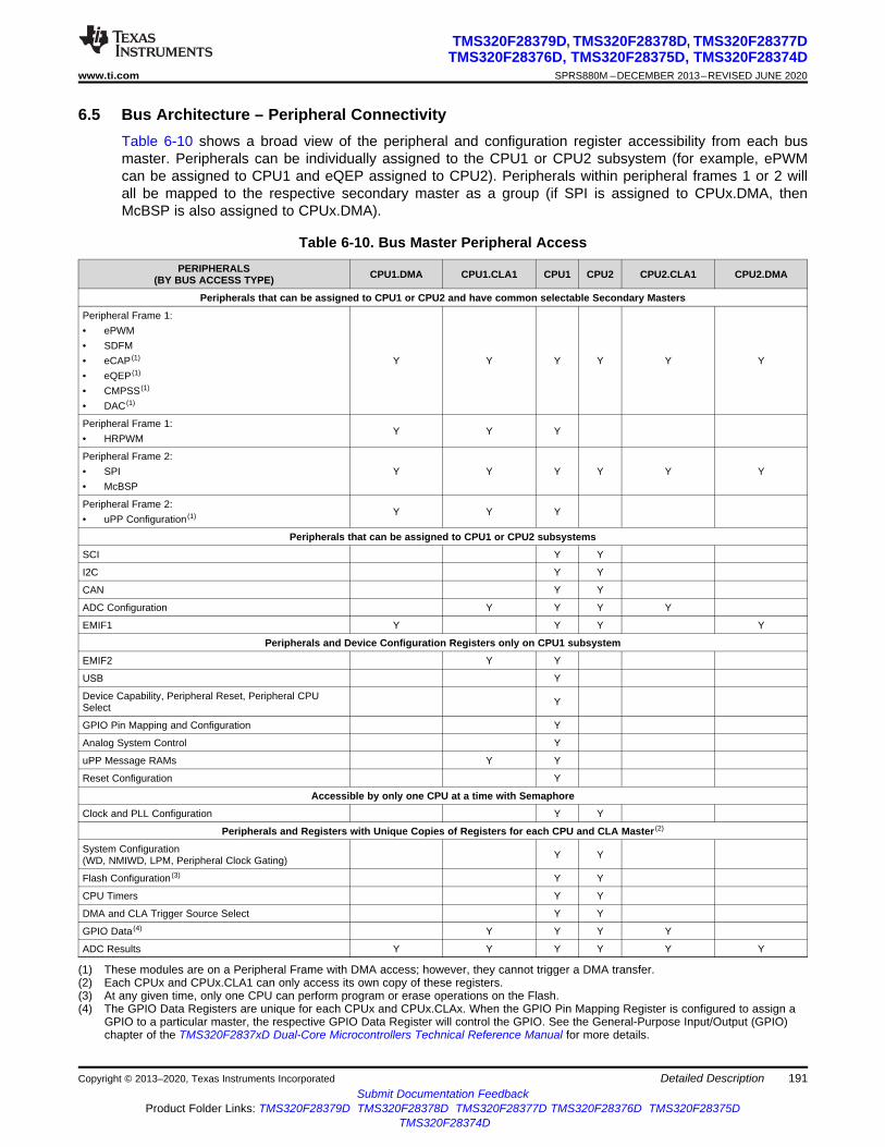
191
TMS320F28379D, TMS320F28378D, TMS320F28377DTMS320F28376D, TMS320F28375D, TMS320F28374D
www.ti.com SPRS880M –DECEMBER 2013–REVISED JUNE 2020
Submit Documentation FeedbackProduct Folder Links: TMS320F28379D TMS320F28378D TMS320F28377D TMS320F28376D TMS320F28375D
TMS320F28374D
Detailed DescriptionCopyright © 2013–2020, Texas Instruments Incorporated
(1) These modules are on a Peripheral Frame with DMA access; however, they cannot trigger a DMA transfer.(2) Each CPUx and CPUx.CLA1 can only access its own copy of these registers.(3) At any given time, only one CPU can perform program or erase operations on the Flash.(4) The GPIO Data Registers are unique for each CPUx and CPUx.CLAx. When the GPIO Pin Mapping Register is configured to assign a
GPIO to a particular master, the respective GPIO Data Register will control the GPIO. See the General-Purpose Input/Output (GPIO)chapter of the TMS320F2837xD Dual-Core Microcontrollers Technical Reference Manual for more details.
6.5 Bus Architecture – Peripheral ConnectivityTable 6-10 shows a broad view of the peripheral and configuration register accessibility from each busmaster. Peripherals can be individually assigned to the CPU1 or CPU2 subsystem (for example, ePWMcan be assigned to CPU1 and eQEP assigned to CPU2). Peripherals within peripheral frames 1 or 2 willall be mapped to the respective secondary master as a group (if SPI is assigned to CPUx.DMA, thenMcBSP is also assigned to CPUx.DMA).
Table 6-10. Bus Master Peripheral AccessPERIPHERALS
(BY BUS ACCESS TYPE) CPU1.DMA CPU1.CLA1 CPU1 CPU2 CPU2.CLA1 CPU2.DMA
Peripherals that can be assigned to CPU1 or CPU2 and have common selectable Secondary Masters
Peripheral Frame 1:• ePWM• SDFM• eCAP (1)
• eQEP (1)
• CMPSS (1)
• DAC (1)
Y Y Y Y Y Y
Peripheral Frame 1:• HRPWM
Y Y Y
Peripheral Frame 2:• SPI• McBSP
Y Y Y Y Y Y
Peripheral Frame 2:• uPP Configuration (1) Y Y Y
Peripherals that can be assigned to CPU1 or CPU2 subsystems
SCI Y Y
I2C Y Y
CAN Y Y
ADC Configuration Y Y Y Y
EMIF1 Y Y Y Y
Peripherals and Device Configuration Registers only on CPU1 subsystem
EMIF2 Y Y
USB Y
Device Capability, Peripheral Reset, Peripheral CPUSelect Y
GPIO Pin Mapping and Configuration Y
Analog System Control Y
uPP Message RAMs Y Y
Reset Configuration Y
Accessible by only one CPU at a time with Semaphore
Clock and PLL Configuration Y Y
Peripherals and Registers with Unique Copies of Registers for each CPU and CLA Master (2)
System Configuration(WD, NMIWD, LPM, Peripheral Clock Gating) Y Y
Flash Configuration (3) Y Y
CPU Timers Y Y
DMA and CLA Trigger Source Select Y Y
GPIO Data (4) Y Y Y Y
ADC Results Y Y Y Y Y Y
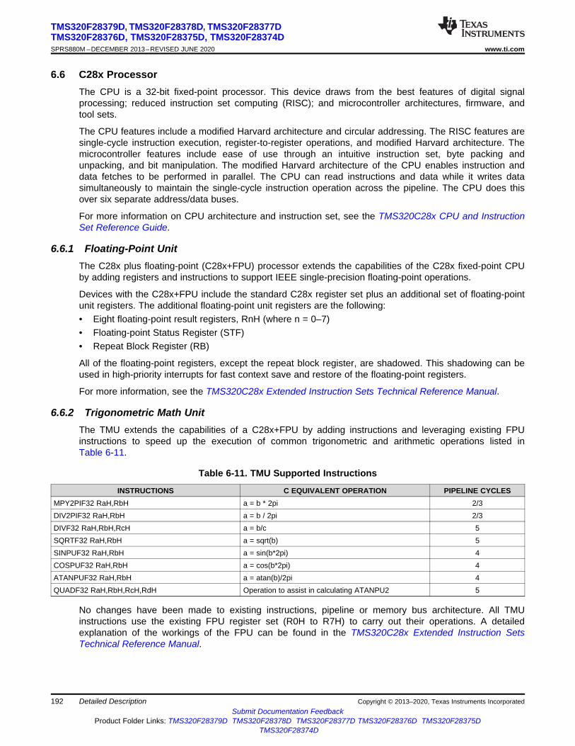
192
TMS320F28379D, TMS320F28378D, TMS320F28377DTMS320F28376D, TMS320F28375D, TMS320F28374DSPRS880M –DECEMBER 2013–REVISED JUNE 2020 www.ti.com
Submit Documentation FeedbackProduct Folder Links: TMS320F28379D TMS320F28378D TMS320F28377D TMS320F28376D TMS320F28375D
TMS320F28374D
Detailed Description Copyright © 2013–2020, Texas Instruments Incorporated
6.6 C28x ProcessorThe CPU is a 32-bit fixed-point processor. This device draws from the best features of digital signalprocessing; reduced instruction set computing (RISC); and microcontroller architectures, firmware, andtool sets.
The CPU features include a modified Harvard architecture and circular addressing. The RISC features aresingle-cycle instruction execution, register-to-register operations, and modified Harvard architecture. Themicrocontroller features include ease of use through an intuitive instruction set, byte packing andunpacking, and bit manipulation. The modified Harvard architecture of the CPU enables instruction anddata fetches to be performed in parallel. The CPU can read instructions and data while it writes datasimultaneously to maintain the single-cycle instruction operation across the pipeline. The CPU does thisover six separate address/data buses.
For more information on CPU architecture and instruction set, see the TMS320C28x CPU and InstructionSet Reference Guide.
6.6.1 Floating-Point UnitThe C28x plus floating-point (C28x+FPU) processor extends the capabilities of the C28x fixed-point CPUby adding registers and instructions to support IEEE single-precision floating-point operations.
Devices with the C28x+FPU include the standard C28x register set plus an additional set of floating-pointunit registers. The additional floating-point unit registers are the following:• Eight floating-point result registers, RnH (where n = 0–7)• Floating-point Status Register (STF)• Repeat Block Register (RB)
All of the floating-point registers, except the repeat block register, are shadowed. This shadowing can beused in high-priority interrupts for fast context save and restore of the floating-point registers.
For more information, see the TMS320C28x Extended Instruction Sets Technical Reference Manual.
6.6.2 Trigonometric Math UnitThe TMU extends the capabilities of a C28x+FPU by adding instructions and leveraging existing FPUinstructions to speed up the execution of common trigonometric and arithmetic operations listed inTable 6-11.
Table 6-11. TMU Supported Instructions
INSTRUCTIONS C EQUIVALENT OPERATION PIPELINE CYCLESMPY2PIF32 RaH,RbH a = b * 2pi 2/3DIV2PIF32 RaH,RbH a = b / 2pi 2/3DIVF32 RaH,RbH,RcH a = b/c 5SQRTF32 RaH,RbH a = sqrt(b) 5SINPUF32 RaH,RbH a = sin(b*2pi) 4COSPUF32 RaH,RbH a = cos(b*2pi) 4ATANPUF32 RaH,RbH a = atan(b)/2pi 4QUADF32 RaH,RbH,RcH,RdH Operation to assist in calculating ATANPU2 5
No changes have been made to existing instructions, pipeline or memory bus architecture. All TMUinstructions use the existing FPU register set (R0H to R7H) to carry out their operations. A detailedexplanation of the workings of the FPU can be found in the TMS320C28x Extended Instruction SetsTechnical Reference Manual.
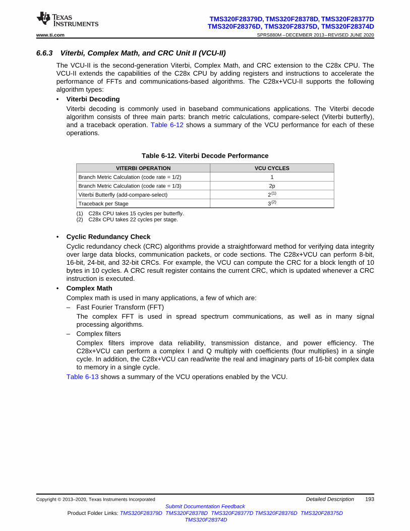
193
TMS320F28379D, TMS320F28378D, TMS320F28377DTMS320F28376D, TMS320F28375D, TMS320F28374D
www.ti.com SPRS880M –DECEMBER 2013–REVISED JUNE 2020
Submit Documentation FeedbackProduct Folder Links: TMS320F28379D TMS320F28378D TMS320F28377D TMS320F28376D TMS320F28375D
TMS320F28374D
Detailed DescriptionCopyright © 2013–2020, Texas Instruments Incorporated
6.6.3 Viterbi, Complex Math, and CRC Unit II (VCU-II)The VCU-II is the second-generation Viterbi, Complex Math, and CRC extension to the C28x CPU. TheVCU-II extends the capabilities of the C28x CPU by adding registers and instructions to accelerate theperformance of FFTs and communications-based algorithms. The C28x+VCU-II supports the followingalgorithm types:• Viterbi Decoding
Viterbi decoding is commonly used in baseband communications applications. The Viterbi decodealgorithm consists of three main parts: branch metric calculations, compare-select (Viterbi butterfly),and a traceback operation. Table 6-12 shows a summary of the VCU performance for each of theseoperations.
(1) C28x CPU takes 15 cycles per butterfly.(2) C28x CPU takes 22 cycles per stage.
Table 6-12. Viterbi Decode Performance
VITERBI OPERATION VCU CYCLESBranch Metric Calculation (code rate = 1/2) 1Branch Metric Calculation (code rate = 1/3) 2pViterbi Butterfly (add-compare-select) 2 (1)
Traceback per Stage 3 (2)
• Cyclic Redundancy CheckCyclic redundancy check (CRC) algorithms provide a straightforward method for verifying data integrityover large data blocks, communication packets, or code sections. The C28x+VCU can perform 8-bit,16-bit, 24-bit, and 32-bit CRCs. For example, the VCU can compute the CRC for a block length of 10bytes in 10 cycles. A CRC result register contains the current CRC, which is updated whenever a CRCinstruction is executed.
• Complex MathComplex math is used in many applications, a few of which are:– Fast Fourier Transform (FFT)
The complex FFT is used in spread spectrum communications, as well as in many signalprocessing algorithms.
– Complex filtersComplex filters improve data reliability, transmission distance, and power efficiency. TheC28x+VCU can perform a complex I and Q multiply with coefficients (four multiplies) in a singlecycle. In addition, the C28x+VCU can read/write the real and imaginary parts of 16-bit complex datato memory in a single cycle.
Table 6-13 shows a summary of the VCU operations enabled by the VCU.
194
TMS320F28379D, TMS320F28378D, TMS320F28377DTMS320F28376D, TMS320F28375D, TMS320F28374DSPRS880M –DECEMBER 2013–REVISED JUNE 2020 www.ti.com
Submit Documentation FeedbackProduct Folder Links: TMS320F28379D TMS320F28378D TMS320F28377D TMS320F28376D TMS320F28375D
TMS320F28374D
Detailed Description Copyright © 2013–2020, Texas Instruments Incorporated
Table 6-13. Complex Math Performance
COMPLEX MATH OPERATION VCU CYCLES NOTESAdd or Subtract 1 32 +/- 32 = 32-bit (Useful for filters)Add or Subtract 1 16 +/- 32 = 15-bit (Useful for FFT)Multiply 2p 16 x 16 = 32-bitMultiply and Accumulate (MAC) 2p 32 + 32 = 32-bit, 16 x 16 = 32-bitRPT MAC 2p+N Repeat MAC. Single cycle after the first operation.
For more information, see the TMS320C28x Extended Instruction Sets Technical Reference Manual.
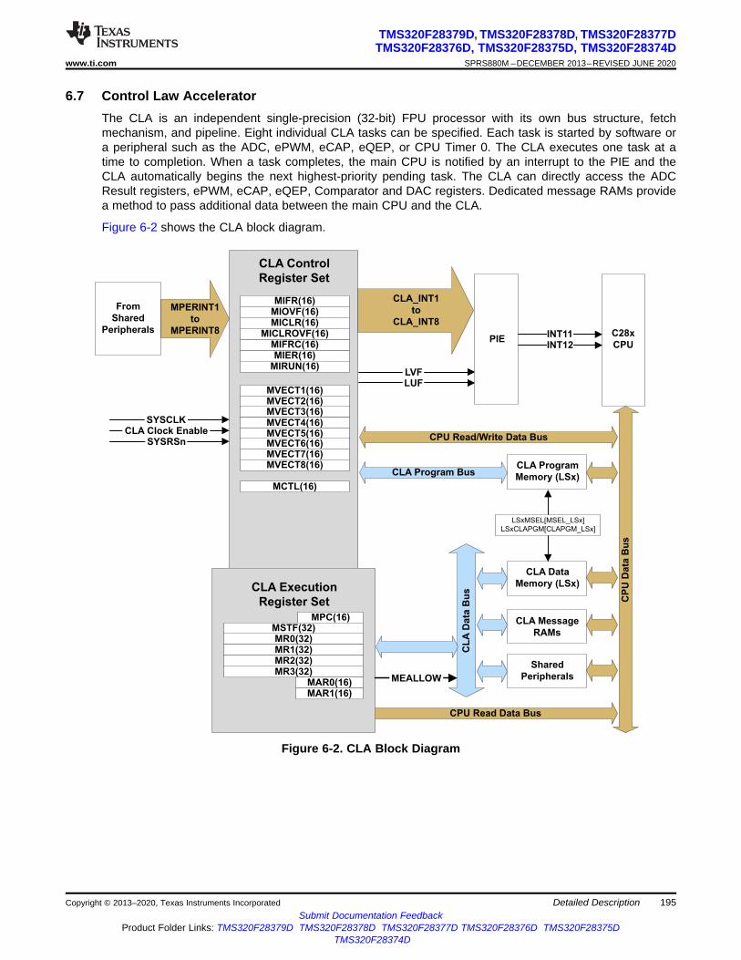
CPU Read Data Bus
MR0(32)
MVECT1(16)
MIFR(16)
MPC(16)
MIER(16)MIFRC(16)
MIRUN(16)
MR1(32)
MR3(32)MAR0(16)
CPU Read/Write Data Bus
CLA Execution
Register Set
CLA Control
Register Set
MSTF(32)
PIE
CLA Program
Memory (LSx)
CLA Data
Memory (LSx)
SYSCLKCLA Clock Enable
SYSRSn
MR2(32)
MAR1(16)
MIOVF(16)MICLR(16)
MCTL(16)
MICLROVF(16)
LUF
CLA Message
RAMs
Shared
PeripheralsMEALLOW
CL
AD
ata
Bu
s
C28x
CPUINT11INT12
MVECT2(16)MVECT3(16)MVECT4(16)MVECT5(16)MVECT6(16)MVECT7(16)MVECT8(16)
CP
U D
ata
Bu
s
LSxMSEL[MSEL_LSx]
LSxCLAPGM[CLAPGM_LSx]
CLA Program Bus
MPERINT1
to
MPERINT8
CLA_INT1
to
CLA_INT8
LVF
From
Shared
Peripherals
195
TMS320F28379D, TMS320F28378D, TMS320F28377DTMS320F28376D, TMS320F28375D, TMS320F28374D
www.ti.com SPRS880M –DECEMBER 2013–REVISED JUNE 2020
Submit Documentation FeedbackProduct Folder Links: TMS320F28379D TMS320F28378D TMS320F28377D TMS320F28376D TMS320F28375D
TMS320F28374D
Detailed DescriptionCopyright © 2013–2020, Texas Instruments Incorporated
6.7 Control Law AcceleratorThe CLA is an independent single-precision (32-bit) FPU processor with its own bus structure, fetchmechanism, and pipeline. Eight individual CLA tasks can be specified. Each task is started by software ora peripheral such as the ADC, ePWM, eCAP, eQEP, or CPU Timer 0. The CLA executes one task at atime to completion. When a task completes, the main CPU is notified by an interrupt to the PIE and theCLA automatically begins the next highest-priority pending task. The CLA can directly access the ADCResult registers, ePWM, eCAP, eQEP, Comparator and DAC registers. Dedicated message RAMs providea method to pass additional data between the main CPU and the CLA.
Figure 6-2 shows the CLA block diagram.
Figure 6-2. CLA Block Diagram
196
TMS320F28379D, TMS320F28378D, TMS320F28377DTMS320F28376D, TMS320F28375D, TMS320F28374DSPRS880M –DECEMBER 2013–REVISED JUNE 2020 www.ti.com
Submit Documentation FeedbackProduct Folder Links: TMS320F28379D TMS320F28378D TMS320F28377D TMS320F28376D TMS320F28375D
TMS320F28374D
Detailed Description Copyright © 2013–2020, Texas Instruments Incorporated
6.8 Direct Memory AccessEach CPU has its own 6-channel DMA module. The DMA module provides a hardware method oftransferring data between peripherals and/or memory without intervention from the CPU, thereby freeingup bandwidth for other system functions. Additionally, the DMA has the capability to orthogonallyrearrange the data as it is transferred as well as “ping-pong” data between buffers. These features areuseful for structuring data into blocks for optimal CPU processing.
The DMA module is an event-based machine, meaning it requires a peripheral or software trigger to starta DMA transfer. Although it can be made into a periodic time-driven machine by configuring a timer as theinterrupt trigger source, there is no mechanism within the module itself to start memory transfersperiodically. The interrupt trigger source for each of the six DMA channels can be configured separatelyand each channel contains its own independent PIE interrupt to let the CPU know when a DMA transferhas either started or completed. Five of the six channels are exactly the same, while Channel 1 has theability to be configured at a higher priority than the others.
DMA features include:• Six channels with independent PIE interrupts• Peripheral interrupt trigger sources
– ADC interrupts and EVT signals– Multichannel buffered serial port transmit and receive– External interrupts– CPU timers– EPWMxSOC signals– SPIx transmit and receive– SDFM– Software trigger
• Data sources and destinations:– GSx RAM– CPU message RAM (IPC RAM)– ADC result registers– ePWMx– SPI– McBSP– EMIF
• Word Size: 16-bit or 32-bit (SPI and McBSP limited to 16-bit)• Throughput: four cycles/word (without arbitration)
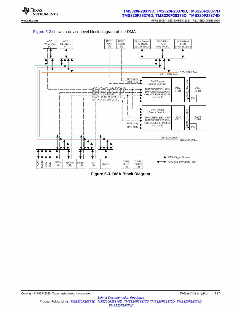
DM
A_C
Hx (
1-6
)D
MA
_C
Hx (
1-6
)
Global Shared16x 4Kx16
GS0-15 RAMs
MSG RAM
CPU2 to CPU11Kx16
MSG RAM
CPU1 to CPU21Kx16
XINT(5)
CPU2TIMER
(3)
CPU2SDFM(8)
EPWM(12)
McBSP(2)
SPI(3)
EMIF1
PIE
PIE
C28x CPU1 BusCPU1.DMA Bus
DMACPU1
C28xCPU1
C28xCPU2
DMACPU2
C28x CPU2 BusCPU2.DMA Bus
XINT (1-5)
TINT (0-2)
SOCA (1-12), SOCB (1-12)
MXEVT (A-B), MREVT (A-B)
SPITX (A-C), SPIRX (A-C)
ADC INT (A-D) (1-4), EVT (A-D)
XINT (1-5)
TINT (0-2)
SDxFLTy (x = 1 to 2, y = 1 to 4)
ADCRESULTS
(4)
ADCWRAPPER
(4)
CPU1XINT(5)
CPU1TIMER
(3)
DMA TriggerSource Selection
DMACHSRCSEL1.CHxDMACHSRCSEL2.CHx
CHx.MODE.PERINTSEL(x = 1 to 6)
DMA TriggerSource Selection
DMACHSRCSEL1.CHxDMACHSRCSEL2.CHx
CHx.MODE.PERINTSEL(x = 1 to 6)
DMA Trigger Source
CPU and DMA Data Path
eQ
EP
eC
AP
CM
PS
S
DA
C
197
TMS320F28379D, TMS320F28378D, TMS320F28377DTMS320F28376D, TMS320F28375D, TMS320F28374D
www.ti.com SPRS880M –DECEMBER 2013–REVISED JUNE 2020
Submit Documentation FeedbackProduct Folder Links: TMS320F28379D TMS320F28378D TMS320F28377D TMS320F28376D TMS320F28375D
TMS320F28374D
Detailed DescriptionCopyright © 2013–2020, Texas Instruments Incorporated
Figure 6-3 shows a device-level block diagram of the DMA.
Figure 6-3. DMA Block Diagram
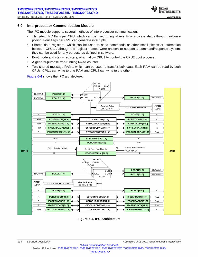
CPU2
Gen Int Pulse
(on FLG 0->1)
Gen Int Pulse
(on FLG 0->1)
SET31
CLR31
FLG31
ACK31
SET0
CLR0
FLG0
ACK0
SET31
CLR31
FLG31
ACK31
SET0
CLR0
FLG0
ACK0
CPU2.EmulationHalt
PLLSYSCLK
R=0/W=1
C1TOC2IPCINT1/2/3/4
R=0/W=1 R=0/W=1
R
R
R
R
R
IPCSET[31:0]
IPCCLR[31:0]
R
R
R
R
R
IPCACK[31:0]
R
IPCSENDCOM[31:0] IPCRECVCOM[31:0]
IPCRECVCOM[31:0]
IPCRECVADDR[31:0]
IPCRECVADDR[31:0]
IPCRECVDATA[31:0]
IPCRECVDATA[31:0]
IPCLOCALREPLY[31:0]
IPCLOCALREPLY[31:0]
IPCSENDADDR[31:0]
IPCSENDADDR[31:0]
IPCSENDDATA[31:0]
IPCSENDDATA[31:0]
R/W
R/W
R/W
R/W
R/W
R/W
R/W
R/W
R
64-bit Free Run Counter
IPCCOUNTERH/L[31:0]
C1TOC2IPCCOM[31:0]
C1TOC2IPCADDR[31:0]
C1TOC2IPCDATAW[31:0]
C1TOC2IPCDATAR[31:0]
R=0/W=1 IPCACK[31:0]
IPCSET[31:0]
IPCCLR[31:0]
RIPCFLG[31:0]
R=0/W=1
R=0/W=1
R IPCSTS[31:0]
C2TOC1IPCCOM[31:0]
C2TOC1IPCADDR[31:0]
C2TOC1IPCDATAW[31:0]
C2TOC1IPCDATAR[31:0]
CPU1
C2TOC1IPCINT1/2/3/4
R
R/W
R/W
R
IPCBOOTMODE[31:0]
IPCBOOTSTS[31:0]
CPU1.EmulationHalt
IPCFLG[31:0]
IPCREMOTEREPLY[31:0]
IPCREMOTEREPLY[31:0]
IPCSTS[31:0]
IPCSENDCOM[31:0]
CPU2.ePIE
CPU1.ePIE
198
TMS320F28379D, TMS320F28378D, TMS320F28377DTMS320F28376D, TMS320F28375D, TMS320F28374DSPRS880M –DECEMBER 2013–REVISED JUNE 2020 www.ti.com
Submit Documentation FeedbackProduct Folder Links: TMS320F28379D TMS320F28378D TMS320F28377D TMS320F28376D TMS320F28375D
TMS320F28374D
Detailed Description Copyright © 2013–2020, Texas Instruments Incorporated
6.9 Interprocessor Communication ModuleThe IPC module supports several methods of interprocessor communication:• Thirty-two IPC flags per CPU, which can be used to signal events or indicate status through software
polling. Four flags per CPU can generate interrupts.• Shared data registers, which can be used to send commands or other small pieces of information
between CPUs. Although the register names were chosen to support a command/response system,they can be used for any purpose as defined in software.
• Boot mode and status registers, which allow CPU1 to control the CPU2 boot process.• A general-purpose free-running 64-bit counter.• Two shared message RAMs, which can be used to transfer bulk data. Each RAM can be read by both
CPUs. CPU1 can write to one RAM and CPU2 can write to the other.
Figure 6-4 shows the IPC architecture.
Figure 6-4. IPC Architecture

199
TMS320F28379D, TMS320F28378D, TMS320F28377DTMS320F28376D, TMS320F28375D, TMS320F28374D
www.ti.com SPRS880M –DECEMBER 2013–REVISED JUNE 2020
Submit Documentation FeedbackProduct Folder Links: TMS320F28379D TMS320F28378D TMS320F28377D TMS320F28376D TMS320F28375D
TMS320F28374D
Detailed DescriptionCopyright © 2013–2020, Texas Instruments Incorporated
6.10 Boot ROM and Peripheral BootingThe device boot ROM (on both the CPUs) contains bootloading software. The CPU1 boot ROM does thesystem initialization before bringing CPU2 out of reset. The device boot ROM is executed each time thedevice comes out of reset. Users can configure the device to boot to flash (using GET mode) or choose toboot the device through one of the bootable peripherals by configuring the boot mode GPIO pins.
The CPU1 boot ROM, being master, owns the boot mode GPIO and boot configurations. The CPU2 bootROM either boots to flash (if configured to do so through user configurable DCSM OTP) or enters a WAITBOOT mode if no OTP is programmed. In WAIT BOOT mode, the CPU1 application instructs the CPU2boot ROM on how to boot further using boot mode IPC commands supported by CPU2 boot ROM.
Table 6-14 shows the possible boot modes supported on the device. The default boot mode pins areGPIO72 (boot mode pin 1) and GPIO 84 (boot mode pin 0). Users may choose to have weak pullups forboot mode pins if they use a peripheral on these pins as well, so the pullups can be overdriven. On thisdevice, customers can change the factory default boot mode pins by programming user configurableDCSM OTP locations. This is recommended only for cases in which the factory default boot mode pins donot fit into the customer design. More details on the locations to be programmed is available in theTMS320F2837xD Dual-Core Microcontrollers Technical Reference Manual.
Table 6-14. Device Boot Mode
MODENO. CPU1 BOOT MODE CPU2 BOOT MODE TRST
GPIO72(BOOTMODEPIN 1)
GPIO84(BOOTMODEPIN 0)
0 Parallel I/O Boot from Master 0 0 01 SCI Mode Boot from Master 0 0 12 Wait Boot Mode Boot from master 0 1 03 Get Mode Boot from Master 0 1 1
4-7 EMU Boot Mode (JTAG debug probeconnected) Boot from Master 1 X X
NOTEThe default behavior of Get mode is boot-to-flash. On unprogrammed devices, using Getmode will result in repeated watchdog resets, which may prevent proper JTAG connectionand device initialization. Use Wait mode or another boot mode for unprogrammed devices.
CAUTION
Some reset sources are internally driven by the device. The user must ensurethe pins used for boot mode are not actively driven by other devices in thesystem for these cases. The boot configuration has a provision for changing theboot pins in OTP. For more details, see the TMS320F2837xD Dual-CoreMicrocontrollers Technical Reference Manual.

200
TMS320F28379D, TMS320F28378D, TMS320F28377DTMS320F28376D, TMS320F28375D, TMS320F28374DSPRS880M –DECEMBER 2013–REVISED JUNE 2020 www.ti.com
Submit Documentation FeedbackProduct Folder Links: TMS320F28379D TMS320F28378D TMS320F28377D TMS320F28376D TMS320F28375D
TMS320F28374D
Detailed Description Copyright © 2013–2020, Texas Instruments Incorporated
6.10.1 EMU Boot or Emulation BootThe CPU enters this boot when it detects that TRST is HIGH (that is, when a JTAG debugprobe/debugger is connected). In this mode, the user can program the EMU_BOOTCTRL control-word (atlocation 0xD00) to instruct the device on how to boot. If the contents of the EMU_BOOTCTRL location areinvalid, then the device would default to WAIT Boot mode. The emulation boot allows users to verify thedevice boot before programming the boot mode into OTP. Note that EMU_BOOTCTRL is not actually aregister, but refers to a location in RAM (PIE RAM). PIE RAM starts at 0xD00, but the first few locationsare reserved (when initializing the PIE vector table in application code) for these boot ROM variables.
6.10.2 WAIT Boot ModeThe device in this boot mode loops in the boot ROM. This mode is useful if users want to connect adebugger on a secure device or if users do not want the device to execute an application in flash yet.
6.10.3 Get ModeThe default behavior of Get mode is boot-to-flash. This behavior can be changed by programming the Zx-OTPBOOTCTRL locations in user configurable DCSM OTP. The user configurable DCSM OTP on thisdevice is divided in to two secure zones: Z1 and Z2. The Get mode function in boot ROM first checks if avalid OTPBOOTCTRL value is programmed in Z1. If the answer is yes, then the device boots as per theZ1-OTPBOOTCTRL location. The Z2-OTPBOOTCTRL location is read and decodes only if Z1-OTPBOOTCTRL is invalid or not programmed. If either Zx-OTPBOOTCTRL location is not programmed,then the device defaults to factory default operation, which is to use factory default boot mode pins to bootto flash if the boot mode pins are set to GET MODE. Users can choose the device through which toboot—SPI, I2C, CAN, and USB—by programming proper values into the user configurable DCSM OTP.More details on this can be found in the TMS320F2837xD Dual-Core Microcontrollers TechnicalReference Manual.
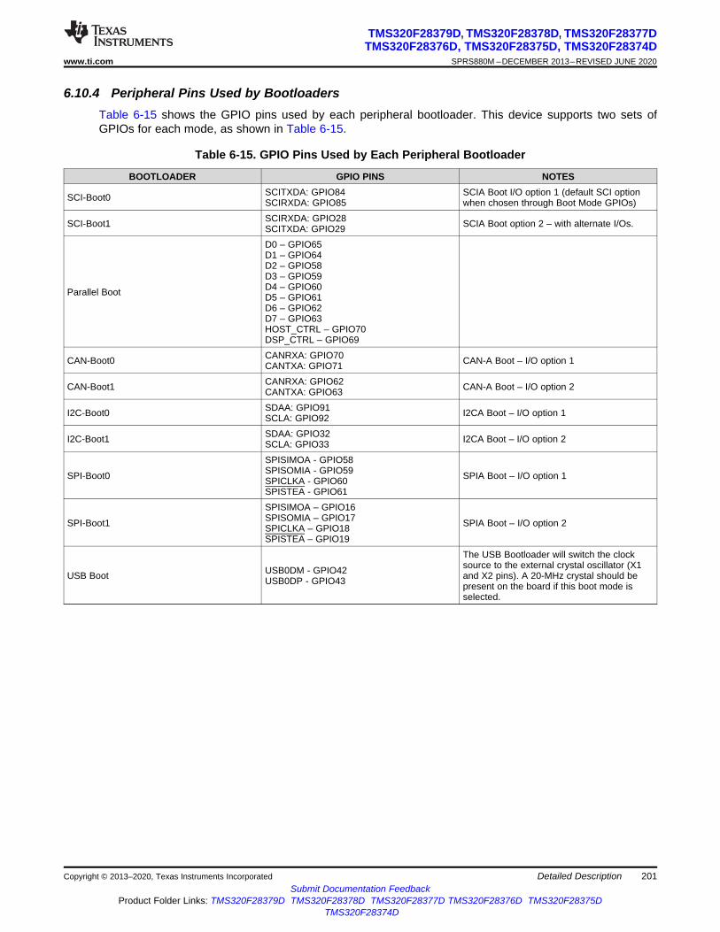
201
TMS320F28379D, TMS320F28378D, TMS320F28377DTMS320F28376D, TMS320F28375D, TMS320F28374D
www.ti.com SPRS880M –DECEMBER 2013–REVISED JUNE 2020
Submit Documentation FeedbackProduct Folder Links: TMS320F28379D TMS320F28378D TMS320F28377D TMS320F28376D TMS320F28375D
TMS320F28374D
Detailed DescriptionCopyright © 2013–2020, Texas Instruments Incorporated
6.10.4 Peripheral Pins Used by BootloadersTable 6-15 shows the GPIO pins used by each peripheral bootloader. This device supports two sets ofGPIOs for each mode, as shown in Table 6-15.
Table 6-15. GPIO Pins Used by Each Peripheral Bootloader
BOOTLOADER GPIO PINS NOTES
SCI-Boot0 SCITXDA: GPIO84SCIRXDA: GPIO85
SCIA Boot I/O option 1 (default SCI optionwhen chosen through Boot Mode GPIOs)
SCI-Boot1 SCIRXDA: GPIO28SCITXDA: GPIO29 SCIA Boot option 2 – with alternate I/Os.
Parallel Boot
D0 – GPIO65D1 – GPIO64D2 – GPIO58D3 – GPIO59D4 – GPIO60D5 – GPIO61D6 – GPIO62D7 – GPIO63HOST_CTRL – GPIO70DSP_CTRL – GPIO69
CAN-Boot0 CANRXA: GPIO70CANTXA: GPIO71 CAN-A Boot – I/O option 1
CAN-Boot1 CANRXA: GPIO62CANTXA: GPIO63 CAN-A Boot – I/O option 2
I2C-Boot0 SDAA: GPIO91SCLA: GPIO92 I2CA Boot – I/O option 1
I2C-Boot1 SDAA: GPIO32SCLA: GPIO33 I2CA Boot – I/O option 2
SPI-Boot0
SPISIMOA - GPIO58SPISOMIA - GPIO59SPICLKA - GPIO60SPISTEA - GPIO61
SPIA Boot – I/O option 1
SPI-Boot1
SPISIMOA – GPIO16SPISOMIA – GPIO17SPICLKA – GPIO18SPISTEA – GPIO19
SPIA Boot – I/O option 2
USB Boot USB0DM - GPIO42USB0DP - GPIO43
The USB Bootloader will switch the clocksource to the external crystal oscillator (X1and X2 pins). A 20-MHz crystal should bepresent on the board if this boot mode isselected.
202
TMS320F28379D, TMS320F28378D, TMS320F28377DTMS320F28376D, TMS320F28375D, TMS320F28374DSPRS880M –DECEMBER 2013–REVISED JUNE 2020 www.ti.com
Submit Documentation FeedbackProduct Folder Links: TMS320F28379D TMS320F28378D TMS320F28377D TMS320F28376D TMS320F28375D
TMS320F28374D
Detailed Description Copyright © 2013–2020, Texas Instruments Incorporated
6.11 Dual Code Security ModuleThe dual code security module (DCSM) prevents access to on-chip secure memories. The term “secure”means access to secure memories and resources is blocked. The term “unsecure” means access isallowed; for example, through a debugging tool such as Code Composer Studio™ (CSS).
The code security mechanism offers protection for two zones, Zone 1 (Z1) and Zone 2 (Z2). The securityimplementation for both the zones is identical. Each zone has its own dedicated secure resource (OTPmemory and secure ROM) and allocated secure resource (CLA, LSx RAM, and flash sectors).
The security of each zone is ensured by its own 128-bit password (CSM password). The password foreach zone is stored in an OTP memory location based on a zone-specific link pointer. The link pointervalue can be changed to program a different set of security settings (including passwords) in OTP.
Code Security Module Disclaimer
THE CODE SECURITY MODULE (CSM) INCLUDED ON THIS DEVICE WAS DESIGNEDTO PASSWORD PROTECT THE DATA STORED IN THE ASSOCIATED MEMORY AND ISWARRANTED BY TEXAS INSTRUMENTS (TI), IN ACCORDANCE WITH ITS STANDARDTERMS AND CONDITIONS, TO CONFORM TO TI'S PUBLISHED SPECIFICATIONS FORTHE WARRANTY PERIOD APPLICABLE FOR THIS DEVICE.
TI DOES NOT, HOWEVER, WARRANT OR REPRESENT THAT THE CSM CANNOT BECOMPROMISED OR BREACHED OR THAT THE DATA STORED IN THE ASSOCIATEDMEMORY CANNOT BE ACCESSED THROUGH OTHER MEANS. MOREOVER, EXCEPTAS SET FORTH ABOVE, TI MAKES NO WARRANTIES OR REPRESENTATIONSCONCERNING THE CSM OR OPERATION OF THIS DEVICE, INCLUDING ANY IMPLIEDWARRANTIES OF MERCHANTABILITY OR FITNESS FOR A PARTICULAR PURPOSE.
IN NO EVENT SHALL TI BE LIABLE FOR ANY CONSEQUENTIAL, SPECIAL, INDIRECT,INCIDENTAL, OR PUNITIVE DAMAGES, HOWEVER CAUSED, ARISING IN ANY WAYOUT OF YOUR USE OF THE CSM OR THIS DEVICE, WHETHER OR NOT TI HAS BEENADVISED OF THE POSSIBILITY OF SUCH DAMAGES. EXCLUDED DAMAGES INCLUDE,BUT ARE NOT LIMITED TO LOSS OF DATA, LOSS OF GOODWILL, LOSS OF USE ORINTERRUPTION OF BUSINESS OR OTHER ECONOMIC LOSS.

203
TMS320F28379D, TMS320F28378D, TMS320F28377DTMS320F28376D, TMS320F28375D, TMS320F28374D
www.ti.com SPRS880M –DECEMBER 2013–REVISED JUNE 2020
Submit Documentation FeedbackProduct Folder Links: TMS320F28379D TMS320F28378D TMS320F28377D TMS320F28376D TMS320F28375D
TMS320F28374D
Detailed DescriptionCopyright © 2013–2020, Texas Instruments Incorporated
6.12 TimersCPU-Timers 0, 1, and 2 are identical 32-bit timers with presettable periods and with 16-bit clockprescaling. The timers have a 32-bit count-down register that generates an interrupt when the counterreaches zero. The counter is decremented at the CPU clock speed divided by the prescale value setting.When the counter reaches zero, it is automatically reloaded with a 32-bit period value.
CPU-Timer 0 is for general use and is connected to the PIE block. CPU-Timer 1 is also for general useand is connected to INT13 of the CPU. CPU-Timer 2 is reserved for TI-RTOS. It is connected to INT14 ofthe CPU. If TI-RTOS is not being used, CPU-Timer 2 is available for general use.
CPU-Timer 2 can be clocked by any one of the following:• SYSCLK (default)• Internal zero-pin oscillator 1 (INTOSC1)• Internal zero-pin oscillator 2 (INTOSC2)• X1 (XTAL)• AUXPLLCLK
6.13 Nonmaskable Interrupt With Watchdog Timer (NMIWD)The NMIWD module is used to handle system-level errors. There is an NMIWD module for each CPU.The conditions monitored are:• Missing system clock due to oscillator failure• Uncorrectable ECC error on CPU access to flash memory• Uncorrectable ECC error on CPU, CLA, or DMA access to RAM• Vector fetch error on the other CPU• CPU1 only: Watchdog or NMI watchdog reset on CPU2
If the CPU does not respond to the latched error condition, then the NMI watchdog will trigger a reset aftera programmable time interval. The default time is 65536 SYSCLK cycles.
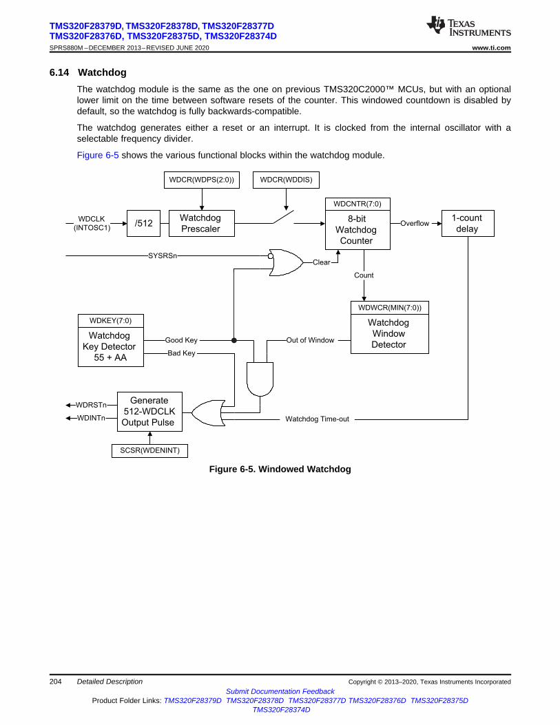
/512WDCLK
(INTOSC1)
Watchdog
Prescaler
WDCR(WDPS(2:0)) WDCR(WDDIS)
SCSR(WDENINT)
1-count
delayOverflow
SYSRSnClear
8-bit
Watchdog
Counter
WDCNTR(7:0)
WDKEY(7:0)
Watchdog
Key Detector
55 + AA
WDWCR(MIN(7:0))
Watchdog
Window
Detector
Count
Good Key
Bad Key
Out of Window
Generate
512-WDCLK
Output Pulse Watchdog Time-out
WDRSTn
WDINTn
204
TMS320F28379D, TMS320F28378D, TMS320F28377DTMS320F28376D, TMS320F28375D, TMS320F28374DSPRS880M –DECEMBER 2013–REVISED JUNE 2020 www.ti.com
Submit Documentation FeedbackProduct Folder Links: TMS320F28379D TMS320F28378D TMS320F28377D TMS320F28376D TMS320F28375D
TMS320F28374D
Detailed Description Copyright © 2013–2020, Texas Instruments Incorporated
6.14 WatchdogThe watchdog module is the same as the one on previous TMS320C2000™ MCUs, but with an optionallower limit on the time between software resets of the counter. This windowed countdown is disabled bydefault, so the watchdog is fully backwards-compatible.
The watchdog generates either a reset or an interrupt. It is clocked from the internal oscillator with aselectable frequency divider.
Figure 6-5 shows the various functional blocks within the watchdog module.
Figure 6-5. Windowed Watchdog

205
TMS320F28379D, TMS320F28378D, TMS320F28377DTMS320F28376D, TMS320F28375D, TMS320F28374D
www.ti.com SPRS880M –DECEMBER 2013–REVISED JUNE 2020
Submit Documentation FeedbackProduct Folder Links: TMS320F28379D TMS320F28378D TMS320F28377D TMS320F28376D TMS320F28375D
TMS320F28374D
Detailed DescriptionCopyright © 2013–2020, Texas Instruments Incorporated
6.15 Configurable Logic Block (CLB)The C2000 configurable logic block (CLB) is a collection of blocks that can be interconnected usingsoftware to implement custom digital logic functions or enhance existing on-chip peripherals. The CLB isable to enhance existing peripherals through a set of crossbar interconnections, which provide a high levelof connectivity to existing control peripherals such as enhanced pulse width modulators (ePWM),enhanced capture modules (eCAP), and enhanced quadrature encoder pulse modules (eQEP). Thecrossbars also allow the CLB to be connected to external GPIO pins. In this way, the CLB can beconfigured to interact with device peripherals to perform small logical functions such as comparators, or toimplement custom serial data exchange protocols. Through the CLB, functions that would otherwise beaccomplished using external logic devices can now be implemented inside the MCU.
The CLB peripheral is configured through the CLB tool. For more information on the CLB tool, availableexamples, application reports and users guide, please refer to the following location in your C2000Warepackage (C2000Ware_2_00_00_03 and higher):
C2000WARE_INSTALL_LOCATION\utilities\clb_tool\clb_syscfg\docCLB Tool User GuideHow to Design with the C2000™ CLB Application ReportHow to Migrate Custom Logic From an FPGA/CPLD to C2000™ CLB Application Report
The CLB module and its interconnects are shown in Figure 6-6.
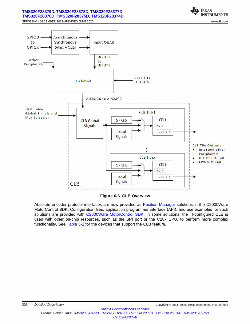
206
TMS320F28379D, TMS320F28378D, TMS320F28377DTMS320F28376D, TMS320F28375D, TMS320F28374DSPRS880M –DECEMBER 2013–REVISED JUNE 2020 www.ti.com
Submit Documentation FeedbackProduct Folder Links: TMS320F28379D TMS320F28378D TMS320F28377D TMS320F28376D TMS320F28375D
TMS320F28374D
Detailed Description Copyright © 2013–2020, Texas Instruments Incorporated
Figure 6-6. CLB Overview
Absolute encoder protocol interfaces are now provided as Position Manager solutions in the C2000WareMotorControl SDK. Configuration files, application programmer interface (API), and use examples for suchsolutions are provided with C2000Ware MotorControl SDK. In some solutions, the TI-configured CLB isused with other on-chip resources, such as the SPI port or the C28x CPU, to perform more complexfunctionality. See Table 3-1 for the devices that support the CLB feature.

207
TMS320F28379D, TMS320F28378D, TMS320F28377DTMS320F28376D, TMS320F28375D, TMS320F28374D
www.ti.com SPRS880M –DECEMBER 2013–REVISED JUNE 2020
Submit Documentation FeedbackProduct Folder Links: TMS320F28379D TMS320F28378D TMS320F28377D TMS320F28376D TMS320F28375D
TMS320F28374D
Detailed DescriptionCopyright © 2013–2020, Texas Instruments Incorporated
6.16 Functional SafetyTMS320C2000™ MCUs are equipped with a TI release validation-based C28x and CLA CompilerQualification Kit (CQ-Kit), which is available for free and may be requested at the Compiler QualificationKit web page.
Additionally, C2000™ MCUs are supported by the TI C2000 Support from Embedded Coder fromMathWorks® to generate C2000-optimized code from a Simulink® model. Simulink® enables Model-BasedDesign to ease the systematic compliance process with certified tools, including Embedded Coder®,Simulink® model verification tools, Polyspace® code verification tools, and the IEC Certification Kit for ISO26262 and IEC 61508 compliance. For more information, see the How to Use Simulink for ISO 26262Projects article.
The Error Detection in SRAM Application Report provides technical information about the nature of theSRAM bit cell and bit array, as well as the sources of SRAM failures. It then presents methods formanaging memory failures in electronic systems. This discussion is intended for electronic systemdevelopers or integrators who are interested in improving the robustness of the embedded SRAM.
Functional Safety-Compliant products are developed using an ISO 26262/IEC 61508-compliant hardwaredevelopment process that is independently assessed and certified to meet ASIL D/SIL 3 systematiccapability (see certificate). The TMS320F2837D, TMS320F2837xS, and TMS320F2807x MCUs have beencertified to meet a component-level random hardware capability of ASIL B/SIL 2 (see certificate).
The Functional Safety-Compliant enablers include:• A Functional Safety Manual• A detailed, tunable, quantitative Failure Modes, Effects, and Diagnostics Analysis (FMEDA)• A software diagnostic library that will help shorten the time to implement various software safety
mechanisms• A collection of application reports to help in the development of functionally safe systems.
A functional safety manual that describes all of the hardware and software functional safety mechanismsis available. See the Safety Manual for TMS320F2837xD, TMS320F2837xS, and TMS320F2807x.
A detailed, tunable, fault-injected, quantitative FMEDA that enables the calculation of random hardwaremetrics—as outlined in the International Organization for Standardization ISO 26262 and the InternationalElectrotechnical Commission IEC 61508 for automotive and industrial applications, respectively—is alsoavailable. This tunable FMEDA must be requested; see the C2000™ Package for Automotive andIndustrial MCUs User's Guide.• A white paper outlining the value (or benefit) of a tunable FMEDA is available. See the Functional
Safety: A tunable FMEDA for C2000™ MCUs publication.• Parts 1 and 2 of a five-part FMEDA tuning training are available. See the C2000™ Tunable FMEDA
Training page.Parts 3, 4, and 5 are packaged with the tunable FMEDA, and must be requested.
The C2000 Diagnostic Software Library is a collection of different safety mechanisms designed to detectfaults. These safety mechanisms target different device components, including the C28x core, the controllaw accelerator (CLA), system control, static random access memory (SRAM), flash, and communicationsand control peripherals. The software safety mechanisms leverage available hardware safety featuressuch as the C28x hardware built-in self-test (HWBIST); error detection and correction functionality onmemories; parallel signature analysis circuitry; missing clock detection logic; watchdog counters; andhardware redundancy.
Also included are software functional safety manual, user guides, example projects, and source code tohelp users shorten system integration time. The library package includes a compliance support package(CSP), a series of documents that TI used to develop and test the diagnostic software library. The CSPprovides the necessary documentation and reports to assist users with compliance to functional safetystandards: software safety requirements specifications; a software architecture document; software
208
TMS320F28379D, TMS320F28378D, TMS320F28377DTMS320F28376D, TMS320F28375D, TMS320F28374DSPRS880M –DECEMBER 2013–REVISED JUNE 2020 www.ti.com
Submit Documentation FeedbackProduct Folder Links: TMS320F28379D TMS320F28378D TMS320F28377D TMS320F28376D TMS320F28375D
TMS320F28374D
Detailed Description Copyright © 2013–2020, Texas Instruments Incorporated
module design documents; software module unit test plans; software module unit test documents; staticanalysis reports; unit test reports; dynamic analysis reports; functional test reports; and traceabilitydocuments. Users can use these documents to comply with route 1s (as described in IEC 61508-3,section 7.4.2.12) to reuse a preexisting software element to implement all or part of a safety function. Thecontents of the CSP could also help users make important decisions for overall system safety compliance.
Two application reports offer details about how to develop functionally safe systems with C2000 real-timecontrol devices:• C2000™ Hardware Built-In Self-Test discusses the HWBIST safety mechanism, along with its
functions and features, in the F2807x/F2837xS/F2837xD series of C2000 devices. The report alsoaddresses some system-level considerations when using the HWBIST feature and explains howcustomers can use the diagnostic library on their system.
• C2000™ CPU Memory Built-In Self-Test describes embedded memory validation using the C28xcentral processing unit (CPU) during an active control loop. It discusses system challenges to memoryvalidation as well as the different solutions provided by C2000 devices and software. Finally, itpresents the Diagnostic Library implementations for memory testing.
209
TMS320F28379D, TMS320F28378D, TMS320F28377DTMS320F28376D, TMS320F28375D, TMS320F28374D
www.ti.com SPRS880M –DECEMBER 2013–REVISED JUNE 2020
Submit Documentation FeedbackProduct Folder Links: TMS320F28379D TMS320F28378D TMS320F28377D TMS320F28376D TMS320F28375D
TMS320F28374D
Applications, Implementation, and LayoutCopyright © 2013–2020, Texas Instruments Incorporated
7 Applications, Implementation, and Layout
NOTEInformation in the following sections is not part of the TI component specification, and TIdoes not warrant its accuracy or completeness. TI’s customers are responsible fordetermining suitability of components for their purposes. Customers should validate and testtheir design implementation to confirm system functionality.
7.1 TI Reference DesignThe TI Reference Design Library is a robust reference design library spanning analog, embeddedprocessor, and connectivity. Created by TI experts to help you jump start your system design, allreference designs include schematic or block diagrams, BOMs, and design files to speed your time tomarket. Search and download designs at the Select TI reference designs page.
Industrial Servo Drive and AC Inverter Drive Reference DesignThe DesignDRIVE Development Kit is a reference design for a complete industrial drive directlyconnecting to a three-phase ACI or PMSM motor. Many drive topologies can be created from thecombined control, power, and communications technologies included on this single platform. This platformincludes multiple position sensor interfaces, diverse current sensing techniques, hot-side partitioningoptions, and expansion for safety and industrial Ethernet.
Isolated Current Shunt and Voltage Measurement Reference Design for Motor DrivesThis evaluation kit and reference design implement the AMC130x reinforced isolated delta-sigmamodulators along with integrated Sinc filters in the C2000 TMS320F28377D microcontroller. The designprovides an ability to evaluate the performance of these measurements: three motor currents, threeinverter voltages, and the DC Link voltage. Provided in the kit is firmware to configure the Sinc filters, setthe PLL frequency, and receive data from Sinc filters. A versatile run-time GUI is also provided to help theuser validate the AMC130x performance and supports configuration changes to Sinc filter parameters inthe TMS320F28377D controller.
Isolated, Shunt-Based Current Sensing Reference DesignThis verified TI reference design implements an isolated current sensing data acqusition solution based onthe AMC1304M25 isolated delta-sigma (ΔΣ) modulator and a TMS320F28377D microcontroller. Thiscircuit was designed for shunt-based current measurement applications, which require excellent galvanicisolation and accuracy, such as industrial motor drives, photovoltaic inverters, and energy metering. It iscapable of measuring load currents from –10 A to +10 A with better than 0.3% uncalibrated accuracy, andit also provides dual functionality of a high-resolution channel and an additional overcurrent or short-circuitdetection channel. The design’s functionality and performance were verified against the circuit designgoals by fabricating three PCBs and measuring results for dc and ac input signals.
Differential Signal Conditioning Circuit for Current and Voltage Measurement Using Fluxgate SensorsThis design provides a 4-channel signal conditioning solution for differential ADCs integrated into amicrocontroller measuring motor current using fluxgate sensors. Also provided is an alternativemeasurement circuit with external differential SAR ADCs as well as circuits for high-speed overcurrent andearth fault detection. Proper differential signal conditioning improves noise immunity on critical currentmeasurements in motor drives. This reference design can help increase the effective resolution of theanalog-to-digital conversion, improving motor drive efficiency.

210
TMS320F28379D, TMS320F28378D, TMS320F28377DTMS320F28376D, TMS320F28375D, TMS320F28374DSPRS880M –DECEMBER 2013–REVISED JUNE 2020 www.ti.com
Submit Documentation FeedbackProduct Folder Links: TMS320F28379D TMS320F28378D TMS320F28377D TMS320F28376D TMS320F28375D
TMS320F28374D
Device and Documentation Support Copyright © 2013–2020, Texas Instruments Incorporated
8 Device and Documentation Support
8.1 Device and Development Support Tool NomenclatureTo designate the stages in the product development cycle, TI assigns prefixes to the part numbers of allTMS320™ MCU devices and support tools. Each TMS320 MCU commercial family member has one ofthree prefixes: TMX, TMP, or TMS (for example, TMS320F28379D). Texas Instruments recommends twoof three possible prefix designators for its support tools: TMDX and TMDS. These prefixes representevolutionary stages of product development from engineering prototypes (with TMX for devices and TMDXfor tools) through fully qualified production devices and tools (with TMS for devices and TMDS for tools).
Device development evolutionary flow:
TMX Experimental device that is not necessarily representative of the final device's electricalspecifications
TMP Final silicon die that conforms to the device's electrical specifications but has notcompleted quality and reliability verification
TMS Fully qualified production device
Support tool development evolutionary flow:
TMDX Development-support product that has not yet completed Texas Instruments internalqualification testing
TMDS Fully qualified development-support product
TMX and TMP devices and TMDX development-support tools are shipped against the followingdisclaimer:"Developmental product is intended for internal evaluation purposes."
TMS devices and TMDS development-support tools have been characterized fully, and the quality andreliability of the device have been demonstrated fully. TI's standard warranty applies.
Predictions show that prototype devices (TMX or TMP) have a greater failure rate than the standardproduction devices. Texas Instruments recommends that these devices not be used in any productionsystem because their expected end-use failure rate still is undefined. Only qualified production devices areto be used.
TI device nomenclature also includes a suffix with the device family name. This suffix indicates thepackage type (for example, PTP) and temperature range (for example, T). Figure 8-1 provides a legendfor reading the complete device name for any family member.
For device part numbers and further ordering information, see the TI website (www.ti.com) or contact yourTI sales representative.
For additional description of the device nomenclature markings on the die, see the TMS320F2837xD Dual-Core MCUs Silicon Errata.
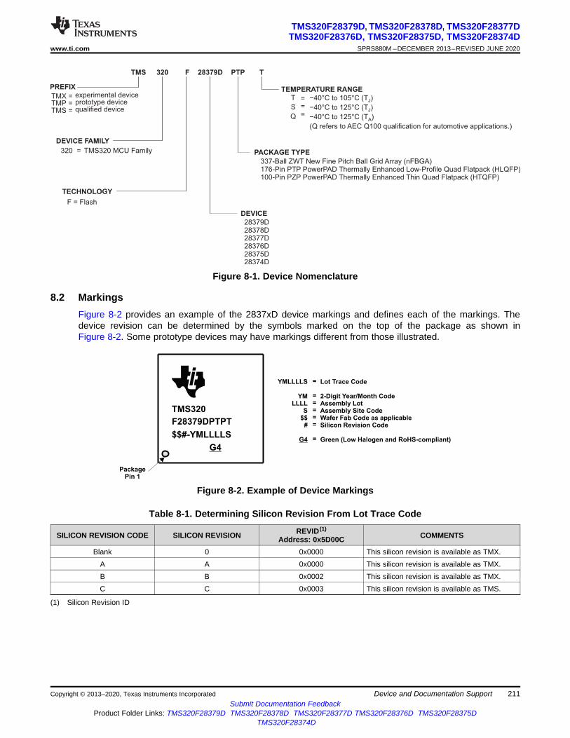
YMLLLLS
YMLLLL
S$$
#
G4
Lot Trace Code
2-Digit Year/Month CodeAssembly LotAssembly Site CodeWafer Fab Code as applicableSilicon Revision Code
Green (Low Halogen and RoHS-compliant)
=
=====
=$$#-YMLLLLS
G4
F28379DPTPT
TMS320
PackagePin 1
PREFIX
TMS
TMX = experimental deviceTMP = prototype deviceTMS = qualified device
320
DEVICE FAMILY
320 = TMS320 MCU Family
F
TECHNOLOGY
F = Flash
28379D
DEVICE
28379D
28377D28376D28375D28374D
28378D
PTP
PACKAGE TYPE
176337-Ball ZWT New Fine Pitch Ball Grid Array (nFBGA)
-Pin PTP PowerPAD Thermally Enhanced Low-Profile Quad Flatpack (HLQFP)100-Pin PZP PowerPAD Thermally Enhanced Thin Quad Flatpack (HTQFP)
TEMPERATURE RANGE
T
−40°C to 105°C (T )
−40°C to 125°C (T )
−40°C to 125°C (T )
(Q refers to AEC Q100 qualification for automotive applications.)
J
J
A
T
S
Q
===
211
TMS320F28379D, TMS320F28378D, TMS320F28377DTMS320F28376D, TMS320F28375D, TMS320F28374D
www.ti.com SPRS880M –DECEMBER 2013–REVISED JUNE 2020
Submit Documentation FeedbackProduct Folder Links: TMS320F28379D TMS320F28378D TMS320F28377D TMS320F28376D TMS320F28375D
TMS320F28374D
Device and Documentation SupportCopyright © 2013–2020, Texas Instruments Incorporated
(1) Silicon Revision ID
Figure 8-1. Device Nomenclature
8.2 MarkingsFigure 8-2 provides an example of the 2837xD device markings and defines each of the markings. Thedevice revision can be determined by the symbols marked on the top of the package as shown inFigure 8-2. Some prototype devices may have markings different from those illustrated.
Figure 8-2. Example of Device Markings
Table 8-1. Determining Silicon Revision From Lot Trace Code
SILICON REVISION CODE SILICON REVISION REVID (1)
Address: 0x5D00C COMMENTS
Blank 0 0x0000 This silicon revision is available as TMX.A A 0x0000 This silicon revision is available as TMX.B B 0x0002 This silicon revision is available as TMX.C C 0x0003 This silicon revision is available as TMS.
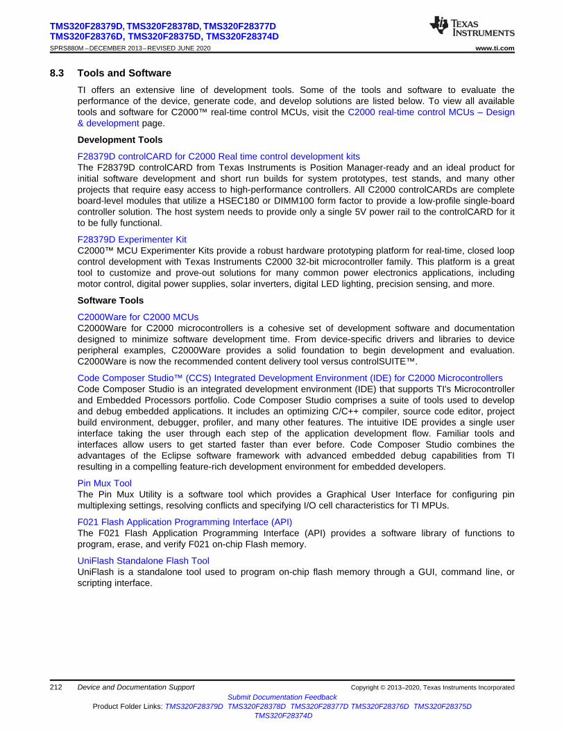
212
TMS320F28379D, TMS320F28378D, TMS320F28377DTMS320F28376D, TMS320F28375D, TMS320F28374DSPRS880M –DECEMBER 2013–REVISED JUNE 2020 www.ti.com
Submit Documentation FeedbackProduct Folder Links: TMS320F28379D TMS320F28378D TMS320F28377D TMS320F28376D TMS320F28375D
TMS320F28374D
Device and Documentation Support Copyright © 2013–2020, Texas Instruments Incorporated
8.3 Tools and SoftwareTI offers an extensive line of development tools. Some of the tools and software to evaluate theperformance of the device, generate code, and develop solutions are listed below. To view all availabletools and software for C2000™ real-time control MCUs, visit the C2000 real-time control MCUs – Design& development page.
Development Tools
F28379D controlCARD for C2000 Real time control development kitsThe F28379D controlCARD from Texas Instruments is Position Manager-ready and an ideal product forinitial software development and short run builds for system prototypes, test stands, and many otherprojects that require easy access to high-performance controllers. All C2000 controlCARDs are completeboard-level modules that utilize a HSEC180 or DIMM100 form factor to provide a low-profile single-boardcontroller solution. The host system needs to provide only a single 5V power rail to the controlCARD for itto be fully functional.
F28379D Experimenter KitC2000™ MCU Experimenter Kits provide a robust hardware prototyping platform for real-time, closed loopcontrol development with Texas Instruments C2000 32-bit microcontroller family. This platform is a greattool to customize and prove-out solutions for many common power electronics applications, includingmotor control, digital power supplies, solar inverters, digital LED lighting, precision sensing, and more.
Software Tools
C2000Ware for C2000 MCUsC2000Ware for C2000 microcontrollers is a cohesive set of development software and documentationdesigned to minimize software development time. From device-specific drivers and libraries to deviceperipheral examples, C2000Ware provides a solid foundation to begin development and evaluation.C2000Ware is now the recommended content delivery tool versus controlSUITE™.
Code Composer Studio™ (CCS) Integrated Development Environment (IDE) for C2000 MicrocontrollersCode Composer Studio is an integrated development environment (IDE) that supports TI's Microcontrollerand Embedded Processors portfolio. Code Composer Studio comprises a suite of tools used to developand debug embedded applications. It includes an optimizing C/C++ compiler, source code editor, projectbuild environment, debugger, profiler, and many other features. The intuitive IDE provides a single userinterface taking the user through each step of the application development flow. Familiar tools andinterfaces allow users to get started faster than ever before. Code Composer Studio combines theadvantages of the Eclipse software framework with advanced embedded debug capabilities from TIresulting in a compelling feature-rich development environment for embedded developers.
Pin Mux ToolThe Pin Mux Utility is a software tool which provides a Graphical User Interface for configuring pinmultiplexing settings, resolving conflicts and specifying I/O cell characteristics for TI MPUs.
F021 Flash Application Programming Interface (API)The F021 Flash Application Programming Interface (API) provides a software library of functions toprogram, erase, and verify F021 on-chip Flash memory.
UniFlash Standalone Flash ToolUniFlash is a standalone tool used to program on-chip flash memory through a GUI, command line, orscripting interface.
213
TMS320F28379D, TMS320F28378D, TMS320F28377DTMS320F28376D, TMS320F28375D, TMS320F28374D
www.ti.com SPRS880M –DECEMBER 2013–REVISED JUNE 2020
Submit Documentation FeedbackProduct Folder Links: TMS320F28379D TMS320F28378D TMS320F28377D TMS320F28376D TMS320F28375D
TMS320F28374D
Device and Documentation SupportCopyright © 2013–2020, Texas Instruments Incorporated
Models
Various models are available for download from the product Tools & Software pages. These include I/OBuffer Information Specification (IBIS) Models and Boundary-Scan Description Language (BSDL) Models.To view all available models, visit the Models section of the Tools & Software page for each device, whichcan be found in Table 8-2.
Training
To help assist design engineers in taking full advantage of the C2000 microcontroller features andperformance, TI has developed a variety of training resources. Utilizing the online training materials anddownloadable hands-on workshops provides an easy means for gaining a complete working knowledge ofthe C2000 microcontroller family. These training resources have been designed to decrease the learningcurve, while reducing development time, and accelerating product time to market. For more information onthe various training resources, visit the C2000™ real-time control MCUs – Support & training site.
Specific F2837xD/F2837xS/F2807x hands-on training resources can be found at C2000™ MCU DeviceWorkshops.

214
TMS320F28379D, TMS320F28378D, TMS320F28377DTMS320F28376D, TMS320F28375D, TMS320F28374DSPRS880M –DECEMBER 2013–REVISED JUNE 2020 www.ti.com
Submit Documentation FeedbackProduct Folder Links: TMS320F28379D TMS320F28378D TMS320F28377D TMS320F28376D TMS320F28375D
TMS320F28374D
Device and Documentation Support Copyright © 2013–2020, Texas Instruments Incorporated
8.4 Documentation SupportTo receive notification of documentation updates, navigate to the device product folder on ti.com. In theupper right corner, click on Alert me to register and receive a weekly digest of any product information thathas changed. For change details, review the revision history included in any revised document.
The current documentation that describes the processor, related peripherals, and other technical collateralis listed below.
Errata
TMS320F2837xD Dual-Core MCUs Silicon Errata describes known advisories on silicon and providesworkarounds.
Technical Reference Manual
TMS320F2837xD Dual-Core Microcontrollers Technical Reference Manual details the integration, theenvironment, the functional description, and the programming models for each peripheral and subsystemin the 2837xD microcontrollers.
CPU User's Guides
TMS320C28x CPU and Instruction Set Reference Guide describes the central processing unit (CPU) andthe assembly language instructions of the TMS320C28x fixed-point digital signal processors (DSPs). ThisReference Guide also describes emulation features available on these DSPs.
TMS320C28x Extended Instruction Sets Technical Reference Manual describes the architecture, pipeline,and instruction set of the TMU, VCU-II, and FPU accelerators.
Peripheral Guides
C2000 Real-Time Control Peripherals Reference Guide describes the peripheral reference guides of the28x DSPs.
Tools Guides
TMS320C28x Assembly Language Tools v20.2.0.LTS User's Guide describes the assembly languagetools (assembler and other tools used to develop assembly language code), assembler directives, macros,common object file format, and symbolic debugging directives for the TMS320C28x device.
TMS320C28x Optimizing C/C++ Compiler v20.2.0.LTS User's Guide describes the TMS320C28x C/C++compiler. This compiler accepts ANSI standard C/C++ source code and produces TMS320 DSP assemblylanguage source code for the TMS320C28x device.
Application Reports
Semiconductor Packing Methodology describes the packing methodologies employed to preparesemiconductor devices for shipment to end users.
Calculating Useful Lifetimes of Embedded Processors provides a methodology for calculating the usefullifetime of TI embedded processors (EPs) under power when used in electronic systems. It is aimed atgeneral engineers who wish to determine if the reliability of the TI EP meets the end system reliabilityrequirement.
An Introduction to IBIS (I/O Buffer Information Specification) Modeling discusses various aspects of IBISincluding its history, advantages, compatibility, model generation flow, data requirements in modeling theinput/output structures and future trends.
Serial Flash Programming of C2000™ Microcontrollers discusses using a flash kernel and ROM loadersfor serial programming a device.
215
TMS320F28379D, TMS320F28378D, TMS320F28377DTMS320F28376D, TMS320F28375D, TMS320F28374D
www.ti.com SPRS880M –DECEMBER 2013–REVISED JUNE 2020
Submit Documentation FeedbackProduct Folder Links: TMS320F28379D TMS320F28378D TMS320F28377D TMS320F28376D TMS320F28375D
TMS320F28374D
Device and Documentation SupportCopyright © 2013–2020, Texas Instruments Incorporated
8.5 Related LinksThe table below lists quick access links. Categories include technical documents, support and communityresources, tools and software, and quick access to order now.
Table 8-2. Related Links
PARTS PRODUCT FOLDER ORDER NOW TECHNICALDOCUMENTS
TOOLS &SOFTWARE
SUPPORT &COMMUNITY
TMS320F28379D Click here Click here Click here Click here Click hereTMS320F28378D Click here Click here Click here Click here Click hereTMS320F28377D Click here Click here Click here Click here Click hereTMS320F28376D Click here Click here Click here Click here Click hereTMS320F28375D Click here Click here Click here Click here Click hereTMS320F28374D Click here Click here Click here Click here Click here
8.6 Support ResourcesTI E2E™ support forums are an engineer's go-to source for fast, verified answers and design help —straight from the experts. Search existing answers or ask your own question to get the quick design helpyou need.
Linked content is provided "AS IS" by the respective contributors. They do not constitute TI specificationsand do not necessarily reflect TI's views; see TI's Terms of Use.
8.7 TrademarksPowerPAD, C2000, Code Composer Studio, TMS320C2000, TMS320, controlSUITE, TI E2E aretrademarks of Texas Instruments.Bosch is a registered trademark of Robert Bosch GmbH Corporation.MathWorks, Simulink, Embedded Coder, Polyspace are registered trademarks of The MathWorks, Inc.All other trademarks are the property of their respective owners.
8.8 Electrostatic Discharge CautionThis integrated circuit can be damaged by ESD. Texas Instruments recommends that all integrated circuits be handled withappropriate precautions. Failure to observe proper handling and installation procedures can cause damage.
ESD damage can range from subtle performance degradation to complete device failure. Precision integrated circuits may be moresusceptible to damage because very small parametric changes could cause the device not to meet its published specifications.
8.9 GlossaryTI Glossary This glossary lists and explains terms, acronyms, and definitions.
216
TMS320F28379D, TMS320F28378D, TMS320F28377DTMS320F28376D, TMS320F28375D, TMS320F28374DSPRS880M –DECEMBER 2013–REVISED JUNE 2020 www.ti.com
Submit Documentation FeedbackProduct Folder Links: TMS320F28379D TMS320F28378D TMS320F28377D TMS320F28376D TMS320F28375D
TMS320F28374D
Mechanical, Packaging, and Orderable Information Copyright © 2013–2020, Texas Instruments Incorporated
9 Mechanical, Packaging, and Orderable Information
9.1 Packaging InformationThe following pages include mechanical, packaging, and orderable information. This information is themost current data available for the designated devices. This data is subject to change without notice andrevision of this document. For browser-based versions of this data sheet, refer to the left-hand navigation.
www.ti.com
PACKAGE OUTLINE
C
100X0.270.1796X 0.5
PIN 1 ID
(0.127)TYP
0.150.050 -7
4X 12
TYP16.215.8
8.647.45
B
NOTE 3
14.213.8
A
NOTE 3
14.213.8
0.750.45
0.25
GAGE PLANE
1.2 MAX
(1)
4X (0.3)NOTE 4
4X (0.3)NOTE 4
PLASTIC QUAD FLATPACK
PowerPAD TQFP - 1.2 mm max heightPZP0100N
4223383/A 04/2017
NOTES:
1. All linear dimensions are in millimeters. Any dimensions in parenthesis are for reference only. Dimensioning and tolerancingper ASME Y14.5M.
2. This drawing is subject to change without notice.3. This dimension does not include mold flash, protrusions, or gate burrs.4. Strap features may not be present.5. Reference JEDEC registration MS-026.
PowerPAD is a trademark of Texas Instruments.
TM
1
25
2650
51
75
76100
0.08 C A B
SEE DETAIL A
SEATING PLANE
DETAIL A
SCALE: 14
DETAIL ATYPICAL
0.08 C
1
SCALE 1.000
25
26 50
51
75
76100
101
217
TMS320F28379D, TMS320F28378D, TMS320F28377DTMS320F28376D, TMS320F28375D, TMS320F28374D
www.ti.com SPRS880M –DECEMBER 2013–REVISED JUNE 2020
Submit Documentation FeedbackProduct Folder Links: TMS320F28379D TMS320F28378D TMS320F28377D TMS320F28376D TMS320F28375D
TMS320F28374D
Mechanical, Packaging, and Orderable InformationCopyright © 2013–2020, Texas Instruments Incorporated
www.ti.com
EXAMPLE BOARD LAYOUT
0.05 MAXALL AROUND
0.05 MINALL AROUND
(15.4)
(15.4)
96X (0.5)
100X (1.5)
100X (0.3)
( 0.2) TYPVIA
( 8.64)
( 12)NOTE 10
(R0.05) TYP
(1) TYP
(1) TYP
PowerPAD TQFP - 1.2 mm max heightPZP0100NPLASTIC QUAD FLATPACK
4223383/A 04/2017
TM
NOTES: (continued)
6. Publication IPC-7351 may have alternate designs.7. Solder mask tolerances between and around signal pads can vary based on board fabrication site.8. This package is designed to be soldered to a thermal pad on the board. See technical brief, Powerpad thermally enhanced package,
Texas Instruments Literature No. SLMA002 (www.ti.com/lit/slma002) and SLMA004 (www.ti.com/lit/slma004).9. Vias are optional depending on application, refer to device data sheet. It is recommended that vias under paste be filled,
plugged or tented.10. Size of metal pad may vary due to creepage requirement.
EXPOSED METAL SHOWNLAND PATTERN EXAMPLE
SCALE:5X
SYMM
SYMM
100 76
26 50
51
751
25
SOLDER MASKDEFINED PAD
METAL COVEREDBY SOLDER MASK
101
SEE DETAILS
METAL
SOLDER MASKOPENING
NON SOLDER MASKDEFINED
SOLDER MASK DETAILS
EXPOSED METAL
SOLDER MASKOPENING
METAL UNDERSOLDER MASK
SOLDER MASKDEFINED
EXPOSED METAL
218
TMS320F28379D, TMS320F28378D, TMS320F28377DTMS320F28376D, TMS320F28375D, TMS320F28374DSPRS880M –DECEMBER 2013–REVISED JUNE 2020 www.ti.com
Submit Documentation FeedbackProduct Folder Links: TMS320F28379D TMS320F28378D TMS320F28377D TMS320F28376D TMS320F28375D
TMS320F28374D
Mechanical, Packaging, and Orderable Information Copyright © 2013–2020, Texas Instruments Incorporated
www.ti.com
EXAMPLE STENCIL DESIGN
( 8.64)
96X (0.5)
100X (1.5)
100X (0.3)
(R0.05) TYP
(15.4)
(15.4)
7.3 X 7.30.175
7.89 X 7.890.150
8.64 X 8.64 (SHOWN)0.125
9.66 X 9.660.1
SOLDER STENCILOPENING
STENCILTHICKNESS
PowerPAD TQFP - 1.2 mm max heightPZP0100NPLASTIC QUAD FLATPACK
4223383/A 04/2017
NOTES: (continued)
11. Laser cutting apertures with trapezoidal walls and rounded corners may offer better paste release. IPC-7525 may have alternatedesign recommendations.
12. Board assembly site may have different recommendations for stencil design.
TM
SOLDER PASTE EXAMPLEEXPOSED PAD
100% PRINTED SOLDER COVERAGE BY AREASCALE:6X
SEE TABLE FORDIFFERENT OPENINGSFOR OTHER STENCILTHICKNESSES
BASED ON0.125 THICK STENCIL
SYMM
SYMM
100 76
26 50
51
751
25
BY SOLDER MASKMETAL COVERED
101
219
TMS320F28379D, TMS320F28378D, TMS320F28377DTMS320F28376D, TMS320F28375D, TMS320F28374D
www.ti.com SPRS880M –DECEMBER 2013–REVISED JUNE 2020
Submit Documentation FeedbackProduct Folder Links: TMS320F28379D TMS320F28378D TMS320F28377D TMS320F28376D TMS320F28375D
TMS320F28374D
Mechanical, Packaging, and Orderable InformationCopyright © 2013–2020, Texas Instruments Incorporated
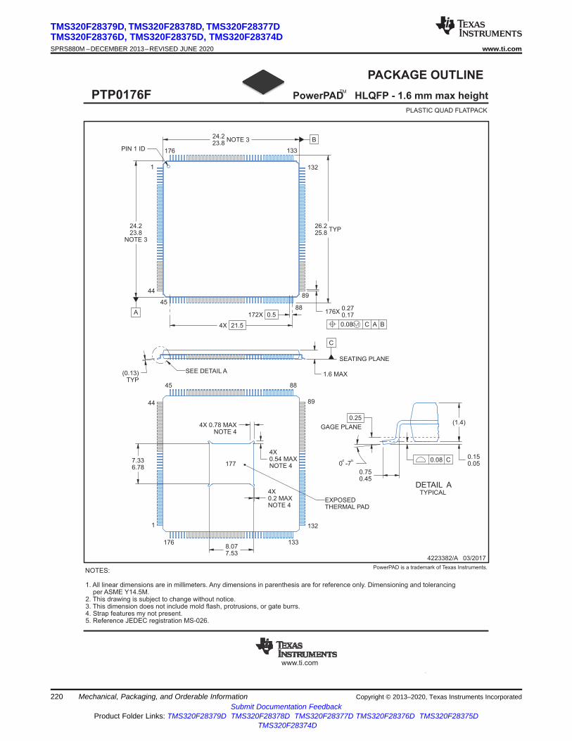
www.ti.com
PACKAGE OUTLINE
C
176X0.270.17172X 0.5
PIN 1 ID
(0.13)TYP
0.150.050 -7
4X 21.5
TYP26.225.8
7.336.78
8.077.53
4X 0.78 MAXNOTE 4
4X0.54 MAXNOTE 4
4X0.2 MAXNOTE 4
BNOTE 324.223.8
A
NOTE 3
24.223.8
0.750.45
0.25
GAGE PLANE
1.6 MAX
(1.4)
PowerPAD HLQFP - 1.6 mm max heightPTP0176FPLASTIC QUAD FLATPACK
4223382/A 03/2017
NOTES:
1. All linear dimensions are in millimeters. Any dimensions in parenthesis are for reference only. Dimensioning and tolerancingper ASME Y14.5M.
2. This drawing is subject to change without notice.3. This dimension does not include mold flash, protrusions, or gate burrs.4. Strap features my not present.5. Reference JEDEC registration MS-026.
TM
PowerPAD is a trademark of Texas Instruments.
1
44
4588
89
132
133176
0.08 C A B
SEE DETAIL A
SEATING PLANE
DETAIL A
SCALE: 12
DETAIL ATYPICAL
0.08 C
1
SCALE 0.550
44
45 88
89
132
133176
177
EXPOSEDTHERMAL PAD
220
TMS320F28379D, TMS320F28378D, TMS320F28377DTMS320F28376D, TMS320F28375D, TMS320F28374DSPRS880M –DECEMBER 2013–REVISED JUNE 2020 www.ti.com
Submit Documentation FeedbackProduct Folder Links: TMS320F28379D TMS320F28378D TMS320F28377D TMS320F28376D TMS320F28375D
TMS320F28374D
Mechanical, Packaging, and Orderable Information Copyright © 2013–2020, Texas Instruments Incorporated
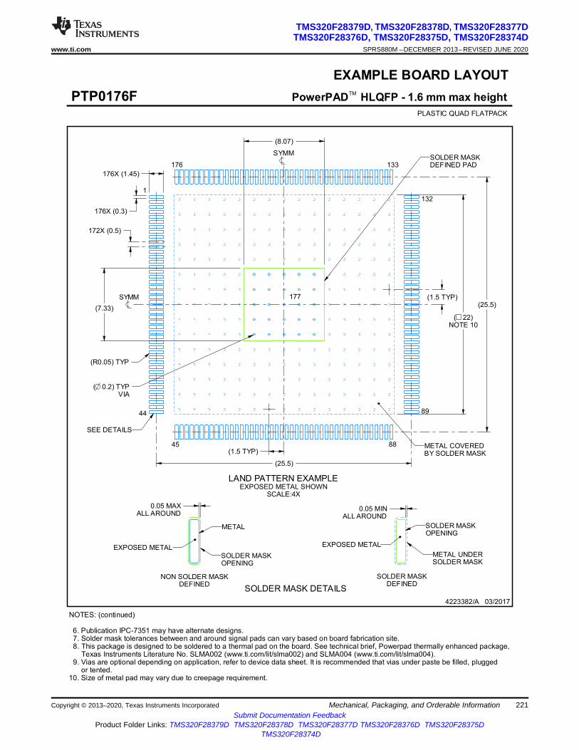
EXAMPLE BOARD LAYOUT
0.05 MAXALL AROUND
0.05 MINALL AROUND
(25.5)
172X (0.5)
176X (1.45)
176X (0.3)
( 0.2) TYPVIA
(8.07)
( 22)NOTE 10
(R0.05) TYP
(1.5 TYP)
(1.5 TYP)
(7.33)(25.5)
PowerPAD HLQFP - 1.6 mm max heightPTP0176FPLASTIC QUAD FLATPACK
4223382/A 03/2017
NOTES: (continued)
6. Publication IPC-7351 may have alternate designs.7. Solder mask tolerances between and around signal pads can vary based on board fabrication site.8. This package is designed to be soldered to a thermal pad on the board. See technical brief, Powerpad thermally enhanced package,
Texas Instruments Literature No. SLMA002 (www.ti.com/lit/slma002) and SLMA004 (www.ti.com/lit/slma004).9. Vias are optional depending on application, refer to device data sheet. It is recommended that vias under paste be filled, plugged
or tented.10. Size of metal pad may vary due to creepage requirement.
TM
LAND PATTERN EXAMPLEEXPOSED METAL SHOWN
SCALE:4X
SYMM
SYMM
176 133
45 88
89
132
1
44
SOLDER MASKDEFINED PAD
METAL COVEREDBY SOLDER MASK
177
SEE DETAILS
METAL
SOLDER MASKOPENING
NON SOLDER MASKDEFINED
SOLDER MASK DETAILS
EXPOSED METAL
SOLDER MASKOPENING
METAL UNDERSOLDER MASK
SOLDER MASKDEFINED
EXPOSED METAL
221
TMS320F28379D, TMS320F28378D, TMS320F28377DTMS320F28376D, TMS320F28375D, TMS320F28374D
www.ti.com SPRS880M –DECEMBER 2013–REVISED JUNE 2020
Submit Documentation FeedbackProduct Folder Links: TMS320F28379D TMS320F28378D TMS320F28377D TMS320F28376D TMS320F28375D
TMS320F28374D
Mechanical, Packaging, and Orderable InformationCopyright © 2013–2020, Texas Instruments Incorporated
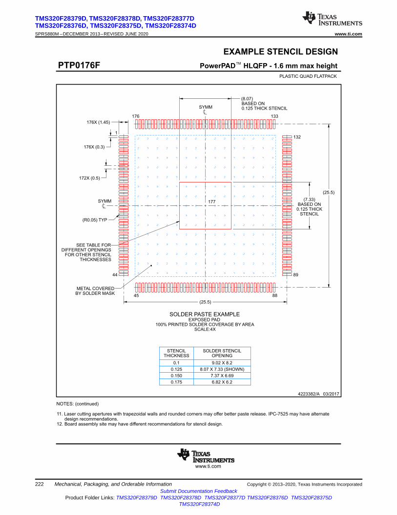
www.ti.com
EXAMPLE STENCIL DESIGN
(8.07)BASED ON0.125 THICK STENCIL
172X (0.5)
176X (1.45)
176X (0.3)
(R0.05) TYP
(25.5)
(25.5)
(7.33)BASED ON
0.125 THICKSTENCIL
6.82 X 6.20.175
7.37 X 6.690.150
8.07 X 7.33 (SHOWN)0.125
9.02 X 8.20.1
SOLDER STENCILOPENING
STENCILTHICKNESS
PowerPAD HLQFP - 1.6 mm max heightPTP0176FPLASTIC QUAD FLATPACK
4223382/A 03/2017
NOTES: (continued)
11. Laser cutting apertures with trapezoidal walls and rounded corners may offer better paste release. IPC-7525 may have alternatedesign recommendations.
12. Board assembly site may have different recommendations for stencil design.
TM
SOLDER PASTE EXAMPLEEXPOSED PAD
100% PRINTED SOLDER COVERAGE BY AREASCALE:4X
THICKNESSESFOR OTHER STENCIL
DIFFERENT OPENINGSSEE TABLE FOR
SYMM
SYMM
176 133
45 88
89
1321
44
BY SOLDER MASKMETAL COVERED
177
222
TMS320F28379D, TMS320F28378D, TMS320F28377DTMS320F28376D, TMS320F28375D, TMS320F28374DSPRS880M –DECEMBER 2013–REVISED JUNE 2020 www.ti.com
Submit Documentation FeedbackProduct Folder Links: TMS320F28379D TMS320F28378D TMS320F28377D TMS320F28376D TMS320F28375D
TMS320F28374D
Mechanical, Packaging, and Orderable Information Copyright © 2013–2020, Texas Instruments Incorporated
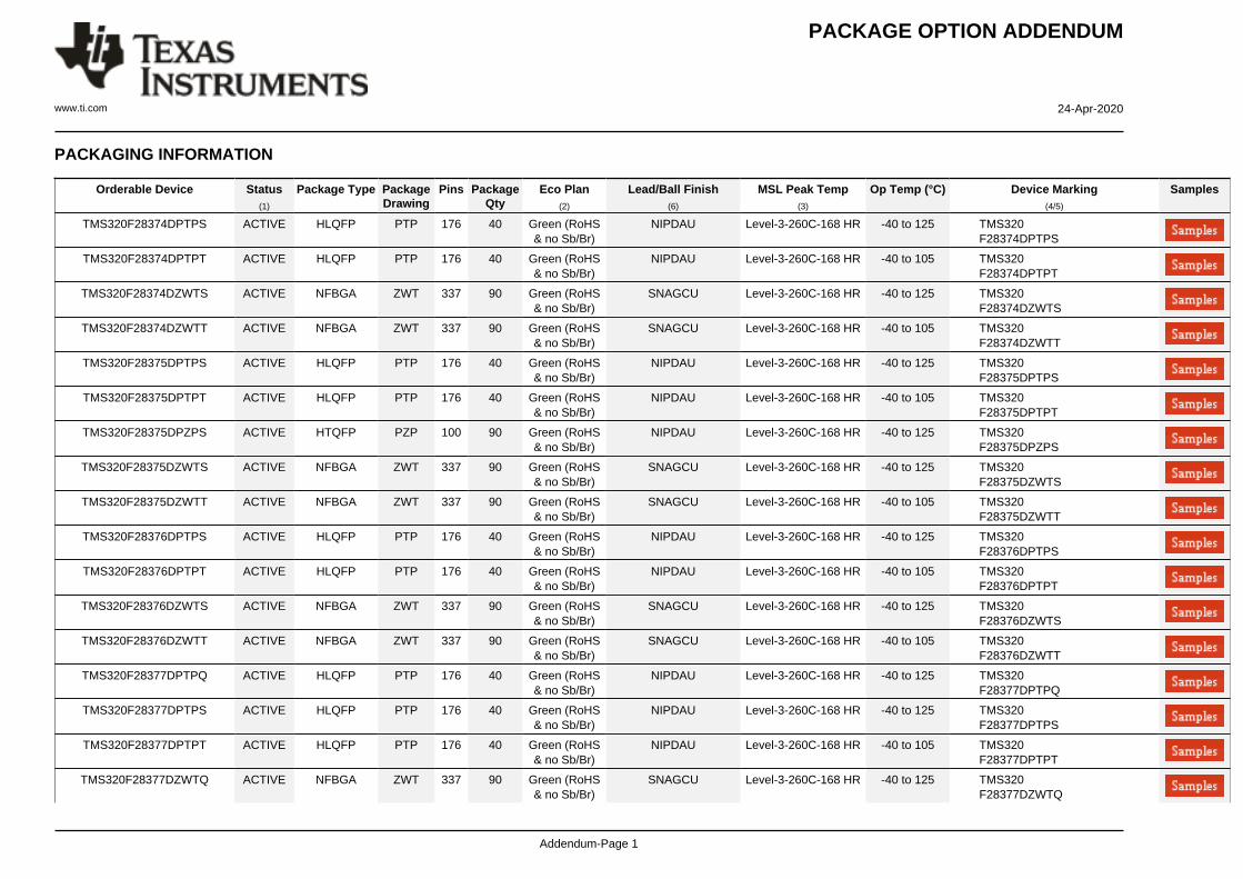
PACKAGE OPTION ADDENDUM
www.ti.com 24-Apr-2020
Addendum-Page 1
PACKAGING INFORMATION
Orderable Device Status(1)
Package Type PackageDrawing
Pins PackageQty
Eco Plan(2)
Lead/Ball Finish(6)
MSL Peak Temp(3)
Op Temp (°C) Device Marking(4/5)
Samples
TMS320F28374DPTPS ACTIVE HLQFP PTP 176 40 Green (RoHS& no Sb/Br)
NIPDAU Level-3-260C-168 HR -40 to 125 TMS320F28374DPTPS
TMS320F28374DPTPT ACTIVE HLQFP PTP 176 40 Green (RoHS& no Sb/Br)
NIPDAU Level-3-260C-168 HR -40 to 105 TMS320F28374DPTPT
TMS320F28374DZWTS ACTIVE NFBGA ZWT 337 90 Green (RoHS& no Sb/Br)
SNAGCU Level-3-260C-168 HR -40 to 125 TMS320F28374DZWTS
TMS320F28374DZWTT ACTIVE NFBGA ZWT 337 90 Green (RoHS& no Sb/Br)
SNAGCU Level-3-260C-168 HR -40 to 105 TMS320F28374DZWTT
TMS320F28375DPTPS ACTIVE HLQFP PTP 176 40 Green (RoHS& no Sb/Br)
NIPDAU Level-3-260C-168 HR -40 to 125 TMS320F28375DPTPS
TMS320F28375DPTPT ACTIVE HLQFP PTP 176 40 Green (RoHS& no Sb/Br)
NIPDAU Level-3-260C-168 HR -40 to 105 TMS320F28375DPTPT
TMS320F28375DPZPS ACTIVE HTQFP PZP 100 90 Green (RoHS& no Sb/Br)
NIPDAU Level-3-260C-168 HR -40 to 125 TMS320F28375DPZPS
TMS320F28375DZWTS ACTIVE NFBGA ZWT 337 90 Green (RoHS& no Sb/Br)
SNAGCU Level-3-260C-168 HR -40 to 125 TMS320F28375DZWTS
TMS320F28375DZWTT ACTIVE NFBGA ZWT 337 90 Green (RoHS& no Sb/Br)
SNAGCU Level-3-260C-168 HR -40 to 105 TMS320F28375DZWTT
TMS320F28376DPTPS ACTIVE HLQFP PTP 176 40 Green (RoHS& no Sb/Br)
NIPDAU Level-3-260C-168 HR -40 to 125 TMS320F28376DPTPS
TMS320F28376DPTPT ACTIVE HLQFP PTP 176 40 Green (RoHS& no Sb/Br)
NIPDAU Level-3-260C-168 HR -40 to 105 TMS320F28376DPTPT
TMS320F28376DZWTS ACTIVE NFBGA ZWT 337 90 Green (RoHS& no Sb/Br)
SNAGCU Level-3-260C-168 HR -40 to 125 TMS320F28376DZWTS
TMS320F28376DZWTT ACTIVE NFBGA ZWT 337 90 Green (RoHS& no Sb/Br)
SNAGCU Level-3-260C-168 HR -40 to 105 TMS320F28376DZWTT
TMS320F28377DPTPQ ACTIVE HLQFP PTP 176 40 Green (RoHS& no Sb/Br)
NIPDAU Level-3-260C-168 HR -40 to 125 TMS320F28377DPTPQ
TMS320F28377DPTPS ACTIVE HLQFP PTP 176 40 Green (RoHS& no Sb/Br)
NIPDAU Level-3-260C-168 HR -40 to 125 TMS320F28377DPTPS
TMS320F28377DPTPT ACTIVE HLQFP PTP 176 40 Green (RoHS& no Sb/Br)
NIPDAU Level-3-260C-168 HR -40 to 105 TMS320F28377DPTPT
TMS320F28377DZWTQ ACTIVE NFBGA ZWT 337 90 Green (RoHS& no Sb/Br)
SNAGCU Level-3-260C-168 HR -40 to 125 TMS320F28377DZWTQ
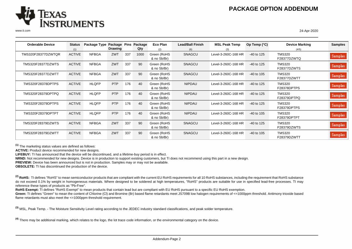
PACKAGE OPTION ADDENDUM
www.ti.com 24-Apr-2020
Addendum-Page 2
Orderable Device Status(1)
Package Type PackageDrawing
Pins PackageQty
Eco Plan(2)
Lead/Ball Finish(6)
MSL Peak Temp(3)
Op Temp (°C) Device Marking(4/5)
Samples
TMS320F28377DZWTQR ACTIVE NFBGA ZWT 337 1000 Green (RoHS& no Sb/Br)
SNAGCU Level-3-260C-168 HR -40 to 125 TMS320F28377DZWTQ
TMS320F28377DZWTS ACTIVE NFBGA ZWT 337 90 Green (RoHS& no Sb/Br)
SNAGCU Level-3-260C-168 HR -40 to 125 TMS320F28377DZWTS
TMS320F28377DZWTT ACTIVE NFBGA ZWT 337 90 Green (RoHS& no Sb/Br)
SNAGCU Level-3-260C-168 HR -40 to 105 TMS320F28377DZWTT
TMS320F28378DPTPS ACTIVE HLQFP PTP 176 40 Green (RoHS& no Sb/Br)
NIPDAU Level-3-260C-168 HR -40 to 125 TMS320F28378DPTPS
TMS320F28379DPTPQ ACTIVE HLQFP PTP 176 40 Green (RoHS& no Sb/Br)
NIPDAU Level-3-260C-168 HR -40 to 125 TMS320F28379DPTPQ
TMS320F28379DPTPS ACTIVE HLQFP PTP 176 40 Green (RoHS& no Sb/Br)
NIPDAU Level-3-260C-168 HR -40 to 125 TMS320F28379DPTPS
TMS320F28379DPTPT ACTIVE HLQFP PTP 176 40 Green (RoHS& no Sb/Br)
NIPDAU Level-3-260C-168 HR -40 to 105 TMS320F28379DPTPT
TMS320F28379DZWTS ACTIVE NFBGA ZWT 337 90 Green (RoHS& no Sb/Br)
SNAGCU Level-3-260C-168 HR -40 to 125 TMS320F28379DZWTS
TMS320F28379DZWTT ACTIVE NFBGA ZWT 337 90 Green (RoHS& no Sb/Br)
SNAGCU Level-3-260C-168 HR -40 to 105 TMS320F28379DZWTT
(1) The marketing status values are defined as follows:ACTIVE: Product device recommended for new designs.LIFEBUY: TI has announced that the device will be discontinued, and a lifetime-buy period is in effect.NRND: Not recommended for new designs. Device is in production to support existing customers, but TI does not recommend using this part in a new design.PREVIEW: Device has been announced but is not in production. Samples may or may not be available.OBSOLETE: TI has discontinued the production of the device.
(2) RoHS: TI defines "RoHS" to mean semiconductor products that are compliant with the current EU RoHS requirements for all 10 RoHS substances, including the requirement that RoHS substancedo not exceed 0.1% by weight in homogeneous materials. Where designed to be soldered at high temperatures, "RoHS" products are suitable for use in specified lead-free processes. TI mayreference these types of products as "Pb-Free".RoHS Exempt: TI defines "RoHS Exempt" to mean products that contain lead but are compliant with EU RoHS pursuant to a specific EU RoHS exemption.Green: TI defines "Green" to mean the content of Chlorine (Cl) and Bromine (Br) based flame retardants meet JS709B low halogen requirements of <=1000ppm threshold. Antimony trioxide basedflame retardants must also meet the <=1000ppm threshold requirement.
(3) MSL, Peak Temp. - The Moisture Sensitivity Level rating according to the JEDEC industry standard classifications, and peak solder temperature.
(4) There may be additional marking, which relates to the logo, the lot trace code information, or the environmental category on the device.

PACKAGE OPTION ADDENDUM
www.ti.com 24-Apr-2020
Addendum-Page 3
(5) Multiple Device Markings will be inside parentheses. Only one Device Marking contained in parentheses and separated by a "~" will appear on a device. If a line is indented then it is a continuationof the previous line and the two combined represent the entire Device Marking for that device.
(6) Lead/Ball Finish - Orderable Devices may have multiple material finish options. Finish options are separated by a vertical ruled line. Lead/Ball Finish values may wrap to two lines if the finishvalue exceeds the maximum column width.
Important Information and Disclaimer:The information provided on this page represents TI's knowledge and belief as of the date that it is provided. TI bases its knowledge and belief on informationprovided by third parties, and makes no representation or warranty as to the accuracy of such information. Efforts are underway to better integrate information from third parties. TI has taken andcontinues to take reasonable steps to provide representative and accurate information but may not have conducted destructive testing or chemical analysis on incoming materials and chemicals.TI and TI suppliers consider certain information to be proprietary, and thus CAS numbers and other limited information may not be available for release.
In no event shall TI's liability arising out of such information exceed the total purchase price of the TI part(s) at issue in this document sold by TI to Customer on an annual basis.
OTHER QUALIFIED VERSIONS OF TMS320F28377D :
• Enhanced Product: TMS320F28377D-EP
NOTE: Qualified Version Definitions:
• Enhanced Product - Supports Defense, Aerospace and Medical Applications

www.ti.com
PACKAGE OUTLINE
C1.4 MAX
TYP0.450.35
14.4TYP
14.4 TYP
0.8 TYP
0.8 TYP
337X 0.550.45
B 16.115.9
A
16.115.9
(0.8) TYP
(0.8) TYP
NFBGA - 1.4 mm max heightZWT0337APLASTIC BALL GRID ARRAY
4223381/A 02/2017
NOTES: 1. All linear dimensions are in millimeters. Any dimensions in parenthesis are for reference only. Dimensioning and tolerancing per ASME Y14.5M. 2. This drawing is subject to change without notice.
13 14 15 16 17 18 19
BALL A1 CORNER
SEATING PLANE
BALL TYP 0.12 C
0.15 C A B0.05 C
SYMM
SYMM
BALL A1 CORNER
W
CDEFGHJKLMNPRTUV
1 2 3 4 5 6 7 8 9 10 11AB
12
SCALE 0.950
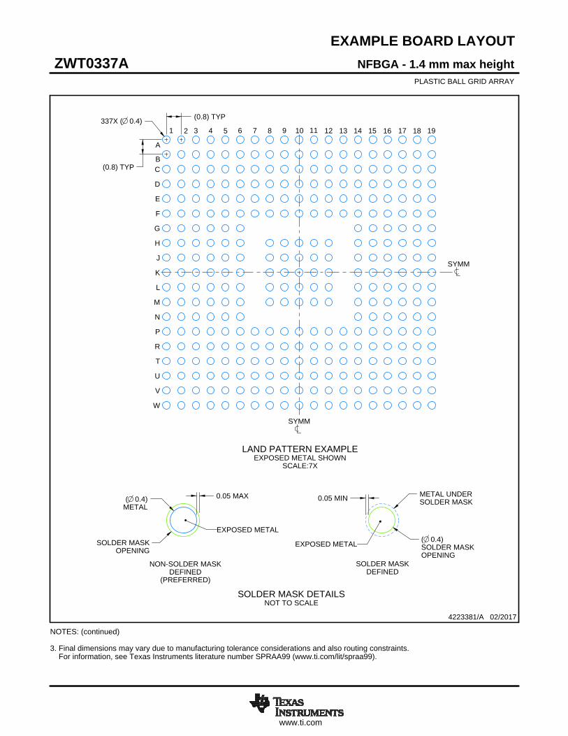
www.ti.com
EXAMPLE BOARD LAYOUT
337X ( 0.4) (0.8) TYP
(0.8) TYP
( 0.4)METAL
0.05 MAX
SOLDER MASKOPENING
METAL UNDERSOLDER MASK
( 0.4)SOLDER MASKOPENING
0.05 MIN
NFBGA - 1.4 mm max heightZWT0337APLASTIC BALL GRID ARRAY
4223381/A 02/2017
NOTES: (continued) 3. Final dimensions may vary due to manufacturing tolerance considerations and also routing constraints. For information, see Texas Instruments literature number SPRAA99 (www.ti.com/lit/spraa99).
SYMM
SYMM
LAND PATTERN EXAMPLEEXPOSED METAL SHOWN
SCALE:7X
1 2 3 4 5 6 7 8 9 10 11
B
A
W
V
U
T
R
P
N
M
L
K
J
H
G
F
E
D
C
12 13 14 15 16 17 18 19
NON-SOLDER MASKDEFINED
(PREFERRED)
SOLDER MASK DETAILSNOT TO SCALE
EXPOSED METAL
SOLDER MASKDEFINED
EXPOSED METAL

www.ti.com
EXAMPLE STENCIL DESIGN
(0.8) TYP
(0.8) TYP ( 0.4) TYP
NFBGA - 1.4 mm max heightZWT0337APLASTIC BALL GRID ARRAY
4223381/A 02/2017
NOTES: (continued) 4. Laser cutting apertures with trapezoidal walls and rounded corners may offer better paste release.
SOLDER PASTE EXAMPLEBASED ON 0.15 mm THICK STENCIL
SCALE:7X
SYMM
SYMM
1 2 3 4 5 6 7 8 9 10 11
B
A
W
V
U
T
R
P
N
M
L
K
J
H
G
F
E
D
C
12 13 14 15 16 17 18 19

IMPORTANT NOTICE AND DISCLAIMER
TI PROVIDES TECHNICAL AND RELIABILITY DATA (INCLUDING DATASHEETS), DESIGN RESOURCES (INCLUDING REFERENCE DESIGNS), APPLICATION OR OTHER DESIGN ADVICE, WEB TOOLS, SAFETY INFORMATION, AND OTHER RESOURCES “AS IS” AND WITH ALL FAULTS, AND DISCLAIMS ALL WARRANTIES, EXPRESS AND IMPLIED, INCLUDING WITHOUT LIMITATION ANY IMPLIED WARRANTIES OF MERCHANTABILITY, FITNESS FOR A PARTICULAR PURPOSE OR NON-INFRINGEMENT OF THIRD PARTY INTELLECTUAL PROPERTY RIGHTS.These resources are intended for skilled developers designing with TI products. You are solely responsible for (1) selecting the appropriate TI products for your application, (2) designing, validating and testing your application, and (3) ensuring your application meets applicable standards, and any other safety, security, or other requirements. These resources are subject to change without notice. TI grants you permission to use these resources only for development of an application that uses the TI products described in the resource. Other reproduction and display of these resources is prohibited. No license is granted to any other TI intellectual property right or to any third party intellectual property right. TI disclaims responsibility for, and you will fully indemnify TI and its representatives against, any claims, damages, costs, losses, and liabilities arising out of your use of these resources.TI’s products are provided subject to TI’s Terms of Sale (www.ti.com/legal/termsofsale.html) or other applicable terms available either on ti.com or provided in conjunction with such TI products. TI’s provision of these resources does not expand or otherwise alter TI’s applicable warranties or warranty disclaimers for TI products.
Mailing Address: Texas Instruments, Post Office Box 655303, Dallas, Texas 75265Copyright © 2020, Texas Instruments Incorporated